EP1422626A2 - Multi-core communications module, data communications system incorporating a multi-core communications module, and data communications process - Google Patents
Multi-core communications module, data communications system incorporating a multi-core communications module, and data communications processDownload PDFInfo
- Publication number
- EP1422626A2 EP1422626A2EP03025909AEP03025909AEP1422626A2EP 1422626 A2EP1422626 A2EP 1422626A2EP 03025909 AEP03025909 AEP 03025909AEP 03025909 AEP03025909 AEP 03025909AEP 1422626 A2EP1422626 A2EP 1422626A2
- Authority
- EP
- European Patent Office
- Prior art keywords
- data
- communications
- fifo
- module
- bus
- Prior art date
- Legal status (The legal status is an assumption and is not a legal conclusion. Google has not performed a legal analysis and makes no representation as to the accuracy of the status listed.)
- Granted
Links
Images


Classifications
- G—PHYSICS
- G06—COMPUTING OR CALCULATING; COUNTING
- G06F—ELECTRIC DIGITAL DATA PROCESSING
- G06F15/00—Digital computers in general; Data processing equipment in general
- G06F15/76—Architectures of general purpose stored program computers
- G06F15/80—Architectures of general purpose stored program computers comprising an array of processing units with common control, e.g. single instruction multiple data processors
- G06F15/8007—Architectures of general purpose stored program computers comprising an array of processing units with common control, e.g. single instruction multiple data processors single instruction multiple data [SIMD] multiprocessors
- G—PHYSICS
- G06—COMPUTING OR CALCULATING; COUNTING
- G06F—ELECTRIC DIGITAL DATA PROCESSING
- G06F13/00—Interconnection of, or transfer of information or other signals between, memories, input/output devices or central processing units
- G06F13/14—Handling requests for interconnection or transfer
- G06F13/16—Handling requests for interconnection or transfer for access to memory bus
- G—PHYSICS
- G06—COMPUTING OR CALCULATING; COUNTING
- G06F—ELECTRIC DIGITAL DATA PROCESSING
- G06F13/00—Interconnection of, or transfer of information or other signals between, memories, input/output devices or central processing units
- G06F13/38—Information transfer, e.g. on bus
- G06F13/40—Bus structure
- G06F13/4004—Coupling between buses
- G06F13/4009—Coupling between buses with data restructuring
- G—PHYSICS
- G06—COMPUTING OR CALCULATING; COUNTING
- G06F—ELECTRIC DIGITAL DATA PROCESSING
- G06F13/00—Interconnection of, or transfer of information or other signals between, memories, input/output devices or central processing units
- G06F13/38—Information transfer, e.g. on bus
- G06F13/40—Bus structure
- G06F13/4004—Coupling between buses
- G06F13/4022—Coupling between buses using switching circuits, e.g. switching matrix, connection or expansion network
Definitions
- This inventionrelates to data communications, and particularly to data communications modules that support data communications between subsystems in multi-core system-on-chips, as well as to systems employing such modules and corresponding data communications processes.
- Data busesare used in integrated circuits (ICs) to transfer data between master devices, such as user-controlled microprocessors, and slave devices controlling peripheral devices, such as memories and the like.
- ICsintegrated circuits
- Such an ICis often referred to as a system-on-chip (SOC).
- SOCssupport multiple processors and are referred to as multi-core SOCs.
- the processors of a multi-core SOCeither do not communicate with each other or use a single, very simple communications mechanism.
- a multi-core SOCmight be configured with two or more processors that either operate in different formats or use a variety of communications mechanisms with each other.
- the SOCis designed to support the requirements of each processor to be coupled by the SOC. For example, if the processors require different hardware resources, or use them in diverse manners, the SOC must be designed to accommodate all such requirements and uses.
- the SOCis designed to accommodate various communications hardware requirements, such as the number and depth of first-in first-out memories (FIFOs), flag and interrupt registers and centralized random-access memories (RAMs), as well as other requirements such as bus protocols, data formats (including endianess), datapath widths, bus frequencies and synchronous/asynchronous communication, to name a few.
- FIFOsfirst-in first-out memories
- RAMscentralized random-access memories
- bus protocolsdata formats (including endianess), datapath widths, bus frequencies and synchronous/asynchronous communication, to name a few.
- multi-core SOCsare designed and fabricated for selected hardware and software requirements of the processors, and are not easily adapted to other processor hardware or software requirements.
- the multi-core SOCsare not easily reconfigurable or programmable to accept processors with different requirements.
- the present inventionis directed to a user-configurable and programmable communications module for a multi-processor system, and particularly for a multi-core SOC, that permits communication between processors having different data and/or address formats or use different communications mechanisms. More particularly, the present invention is directed to a communications module that acts as a slave device for each of a plurality of buses so that processors on one bus can exchange messages, share data, and signal events with processors on other buses.
- the communications moduleincludes a memory addressable in the address format of each bus to write data into the memory from each bus, and to read data to each bus in response to commands from a bus.
- a communications modulefor a data communications system having a plurality of data processors.
- the modulecomprises a plurality of ports, each arranged to be coupled to at least one of the respective data processors.
- a memory devicehas a plurality of locations for storing data that are addressable by the data processors.
- a multiplexertransmits data between an addressed location in the memory and a respective data processor.
- the memory devicecomprises a plurality of addressable FIFOs, and an address table associated with each of the FIFOs associates addresses of the respective FIFO to addresses of the master devices.
- a counter coupled to each FIFOis responsive to the FIFO contents to supply a flag or ready signal indicating the not-full or not-empty status of the respective FIFO.
- the flag or ready signalis supplied to a data processor that is writing data to the FIFO or that is reading data from the FIFO so that the writing data processor will write only when the FIFO is not full and the reading data processor will read only when the FIFO is not empty.
- the moduleincludes an arbiter for arbitrating access to the memory device by the data communications buses.
- the data processorsare master devices coupled to respective data buses.
- Each buscouples a plurality of master devices to a plurality of slave devices so that each master device can transfer data with a slave device via the respective data communications bus.
- the communications moduleis coupled to each bus in a manner similar to a slave device.
- dataare transferred between first and second data processors operating in incompatible formats.
- One data processortransmits data to a communications module using its native format.
- the dataare stored in the communications module, and the other data processor is operated to receive the data from the module device using its native format.
- the first data processoris operated to transmit a first address in a first format to the communications module.
- the communications moduleassociates the first address to a second address that identifies an addressable location in the communications module, where the data are stored. That address is associated to a third address in a second format, and the second data processor is operated to transmit the third address to the communications module.
- the moduleis response to the third address to transmit data from the location identified by the second address to the second data processor.
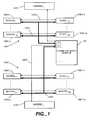
- FIG. 1is a block diagram illustrating a plurality of buses 100/1, 100/2, etc. coupled to a communications module 102, such as a multi-core communications module.
- Bus system 100/1includes a plurality of master devices 104/1-1... 104/1-n and a plurality of slave devices 106/1-1... 106/1-m.
- a data bus 108/1couples the master devices 104/1 to the slave devices 106/1 as well as to a first port P-1 of module 102.
- a control bus 110/1couples each of the master devices 104/1 to each of the slave devices 106/1, port P-1 of module 102, and to arbiter 112/1 of bus system 101/1.
- bus system 100/2includes a plurality of master devices 104/2-1... 104/2-n and a plurality of slave devices 106/2-1... 106/2-m.
- a data bus 108/2couples the master devices 104/2 to the slave devices 106/2 as well as to a second port P-2 of module 102.
- Control bus 110/2couples each of the master devices 104/2 to each of the slave devices 106/2, port P-2 of module 102, and to arbiter 112/2 of bus system 100/2.
- Bus systems 100are data bus systems that transfer data between master devices 104 and slave devices 106 under control of an arbiter 112.
- a bus system 100is an Advanced High-performance Bus (AHB) based on a design from ARM Limited of Cambridge, England.
- the AHB busis a form of an Advanced Microcontroller Bus Architecture (AMBA) bus that provides high performance, high clock frequency data transfer between multiple bus master devices and multiple bus slave devices through use of an arbiter.
- the AHB busis particularly useful in integrated circuit chips, including single chip processors, to couple processors to on-chip memories and to off-chip external memory interfaces.
- the AHB busis a synchronous pipelined bus that operates in two phases, a command phase followed by a data transfer phase.
- a master device 104initiates the command phase, such as by instructing a slave device 106 that the master device desires to write data to the slave device's memory or by instructing the slave device that the master device desires to read data from the slave device's memory.
- slave device 106When slave device 106 is ready to receive data for storage, or is ready to send recovered data to the master device, it notifies arbiter 112 and master device 104 it is ready to receive or send data. The data transfer is then performed.
- the data transferis ordinarily performed on a 32- or 64-bit data bus capable of transferring a plurality of 8-bit bytes of data (4 bytes, in the case of 32-bit buses and 8 bytes in the case of 64-bit buses).
- Control signals that define the nature and format of the data transferare transferred between the master and slave devices and the arbiter via control lines.
- a more detailed description of the AHB bus designmay be found in AMBA Specification published by ARM Limited (1999), Version 2.0, and particularly Chapter 3 thereof (pp. 3-1 to 3-58), incorporated herein by reference.
- AHB bus designThere are multiple configurations of the AHB bus design, each with different formats. Some AHB buses employ 32-bit data buses while others employ 64-bit buses; some AHB buses employ a "big endian” address format, while others employ a "little endian” address format. AHB buses are not ordinarily able to handle more than sixteen master devices. Moreover, a given AHB bus system 100 usually operates in a single format, such as 32- or 64-bit data transfers, with big endian or little endian address formats. Module 102 acts as an additional slave device to each bus.
- FIG. 2is a block diagram of communications module 102 in accordance with an embodiment of the present invention.
- Module 102includes a plurality of data ports 120/1, 120/2, 120/3,... 120/x each coupled to a respective one of the data buses 108/1, 108/2, 108/3,... 108/x and control buses 106/1, 106/2, 106/3,... 106/x of a respective bus system 100/1, 100/2, 100/3,... 100/x.
- Each port 120receives data and control signals from a respective bus 108 and supplies them to multiplexer 122 via a respective bus 124/1, 124/2,... 124/x.
- Multiplexer 122supplies data to first-in first-out (FIFO) memory 126, flag register 128 and random access memory 130 (SRAM).
- Arbiter 132arbitrates use of multiplexer 122, and particularly access of ports 120 to multiplexer 122 and the memory space of FIFO 126, register 128 and SRAM 130.
- FIFO 126 and SRAM 130provide data outputs via local bus 134 to each port 120, and FIFO 126 and flag register 128 provide status outputs via bus 136 to ports 120 to supply control data via control buses 106 to the respective data bus 100.
- Configuration register 138is coupled to arbiter 132, FIFOs 126 and flag register 128 to provide user-adjustable configuration to the arbiter, FIFO and flag register.
- Module 102is configured to handle a plurality of data buses, and the user has the ability to change the configuration. Message passing mechanisms appear as memory mapped functions in the module memory space provided by FIFO 126 and SRAM 130. Timing of module 102 is provided locally; consequently, module 102 operates at a frequency independent of the frequency of any given data bus 100.
- FIFO 126comprises a plurality of first-in, first-out memories that are coupled to one or more of ports 120.
- the data storage portions of FIFO 126may be physically part of SRAM 130.
- FIFO 126includes control portions, including registers and counters described below, which may be separate from SRAM 130.
- FIFO 126provides cross-coupled data communications between two ports 120 so that one port can write data to a FIFO while a second port can read data from that FIFO.
- a full/empty status flagis provided by the FIFO to the ports for data transfer purposes.
- the port 120 coupled to the busdetermines if the address accompanying the request is to module 102.
- the address issued by a master device on a given busaddressees a particular slave device 106 or communications module 102.
- Each portis responsive to the address or address range of the module assigned for the respective bus 100. It is not necessary that module 102 has the same address or address range to each bus; instead, the address of the module may be different for each bus 100.
- arbiter 132arbitrates which port has use of multiplexer 122 and of the memory space at a given time.
- the arbitration protocolmay be any protocol suitable for the system, including rotation of the priority among the ports or assigning specific ports a priority over others, or a combination of both. It is preferred that any given arbitration cycle prioritizes ports 120 so that if the port with the highest priority does not have any current requests, the port with the next highest priority will be serviced.
- FIG. 3is a functional diagram of FIFO 126 coupled to a plurality of ports 120-1, 120-2, 120-3.
- FIFO 126comprises a plurality of first-in, first-out memories 140, 142, 144, 146, each having a respective base address table 148, 150, 152, 154 that identifies the base address of the respective FIFO and a table of addresses to master devices on other buses.
- a given FIFOmay be dedicated for transfer of data from one specific bus to another, or among a specific group of buses. If a master device 104/1 on bus 100/1 desires to send a message through FIFO 126 to a master device 104/2 on bus 100/2, the message is addressed to a FIFO, for example FIFO 140, and includes an address for master device 104/2 in the format of bus 100/1. Address 148 includes a table that identifies the address of master device 104/2 in the format of bus 100/2. When data are received in FIFO 140, the FIFO issues the associated address of master device 104/2 and a flag through port 120/2 to bus 100/2 to identify that FIFO 140 has data for transfer to master device 104/2 (FIG. 1).
- the flag issued by the FIFOrepresents a response signal from a slave device in a standard AHB bus and is supplied to bus arbiter 112/2 (FIG. 1) to notify the bus arbiter that module 102, acting as a slave device, is ready to transfer data to the master identified by the FIFO.
- Arbiter 112/2arbitrates use of bus 100/2 to allocate use of the bus to the appropriate master device 104/2, whereupon that master device sends a request and its address for FIFO 140 in the format of bus 100/2 to module 102, now acting as a slave device to bus 100/2.
- FIFO 140transfers the data, as a read function, through port 120/2 onto bus 100/2 and to the appropriate master device 104/2 thereon.
- select signalsare received from each data bus 100/1, 100/2.... These select signals are decoded by multiplexer 122 from the address code issued by the respective master device 104/1, 104/2... to identify the address offset for the specific FIFO 140, 142, 144, 146 being addressed.
- the select signalsare generated in the form of HSELx signals compatible to the respective AHB bus.
- a typical address codecontains 32 bits, and addresses specific locations in the slave devices of the respective bus. Typically, the most significant bits address the particular slave device and the least specific bits address the specific location in the slave device with which to transfer data.
- FIG. 4illustrates certain control aspects of a FIFO 140, 142, 144, 146.
- Each FIFO 140, 142, 144, 146includes a write counter 150 and a read counter 152.
- a word or word portionsuch as a byte
- the count in write counter 150is incremented by the byte count.
- read counter 152is incremented.
- Counters 150 and 152are recirculating counters that operate to maintain an incremental count of the full and not-full, and empty and not-empty, status of the FIFO. As data are written into the FIFO by one master device (master 104/1), the count difference is incremented; as data are read out of the FIFO by the other master device (master 104/2), the count difference is decremented. Controller 154 is responsive to counters 150 and 152 to increment and decrement the count difference to provide FIFO not-full and FIFO not-empty flags to the master devices.
- ready signalsare issued when a selected slave device is ready to complete a transaction, such a read or write transaction.
- communications module 102is acting as a slave device to both master devices 104/1 and 104/2 to write data from master device 104/1 and read data to master device 104/2.
- module 102issues a ready signal to writing master device 104/1 when FIFO 140 is not full and issues a ready signal to reading master device 104/2 when FIFO 140 is not empty.
- the ready signal to the writing master device 104/1enables master device 104/1 to transfer of data to the FIFO.
- a ready signal to reading master device 104/2enables master device 104/2 to read data from the FIFO.
- the writing masteris enabled to write into the FIFO only when the FIFO is not full, and the reading master is enabled to read data from the FIFO only when the FIFO is not empty.
- SRAM 130is a general purpose single port SRAM that is used to transfer large blocks of data between two data buses. SRAM 130 is addressed in a manner similar to any other slave device of an AHB bus. More particularly, each master device 104 on a given bus 100 addresses the SRAM using the address assigned to the module for the bus (which may be different for each bus) and the offset address for the addressable location within the SRAM to which the master device desires to access. For example, if module 102 has the address 40xx_xxxx to bus 100/1, a master device 104/1 on bus 100/1 will address the memory space of module 102 using addresses 40xx_xxxx.
- SRAM 130might have the address xx00_xxxx, so master device will use the address 4000_xxxx to address the SRAM, where xxxx designates a particular addressable location within the SRAM. Similarly, if module 102 has the address 30xx_xxxx to bus 100/2, a master device 104/2 on bus 100/2 will address the SRAM 130 using address 3000_xxxx.
- Flag register 128is addressed by each master device 104 in a manner similar to addressing the FIFOs. More particularly, in preferred embodiments a flag register is used for addressing from one port 120 to another port 120. The flag register may be used to indicate the presence of data in SRAM 130 so that a transmitting one master device may notify a master device on another bus that data are present for it.
- FIG. 5is a logical diagram illustrating the operation of multi-core communication module 102 with plural data processors, such as a processor on a bus 100.
- data processors 160, 162 and 164which may represent respective buses, are operable to address locations in a random access area 166, representing SRAM memory 130 (FIG. 2), via two-way communications.
- each processoris able to write data to, and read data from, random access area 166 through multiplexer 122 (FIG. 2).
- the FIFOsare preferably arranged for one-way communication from one processor (or bus) to another processor (or bus).
- each processoris able to send data or messages through a FIFO and multiplexer 122 (FIG. 2) to another processor.
- processor 160can send data or messages through multiplexer 122 to FIFO 168 for access through multiplexer 122 to processor 162.
- processor (or bus) 162can send messages through FIFO 170 to processor (or bus) 160
- processors (or buses) 160 and 164can exchange data and messages through FIFOs 172 and 174
- processors (or buses) 162 and 164can exchange data and messages through FIFOs 176 and 178.
- processors (or buses) 160 and 162can send flags to each other through flag registers 180 and 182
- processors (or buses) 162 and 164can send flags to each other through flag registers 184 and 186
- processors (or buses) 160 and 164can send flags to each other through flag registers 188 and 190.
- the memorycan be implemented as a single ported memory which uses an arbitrated front end to identify which processor will get access.
- the memorymay be implemented as a multi-port memory. Advantages of the single ported memory include that it is small, can operate at a higher frequency and can be more easily managed by hardware to prevent simultaneous access by two processors to the same memory location.
- Communications module 102is configurable (programmable) using configuration register 138.
- Register 138contains user modifiable code to change the arbitration rules of arbiter 132, settings of flag register 128 and control of FIFO 126.
- FIFOs 140,...may be programmed to transfer data between two or more specific buses 100.
- a given FIFOmay be configured to write data only from master devices on bus 100/1 and read data only to bus 100/2, or to transfer (write and read) data in both directions between buses 100/1 and 100/2, or to transfer data amongst any of several buses, or in any other useful configuration desired by the user.
- module 102One feature of the invention resides in the ability of module 102 to receive and issue commands in the native format of the respective bus. More particularly, address mapping for the FIFO is accomplished using the address tables. Multiplexer 122 allocates use of the module as arbitrated by arbiter 132. Communications module 102 supports various bus formats, such as big endian and little endian address formats. Preferably, module 102 itself operates in little endian format. (In the big endian format, the bytes are numbered from left to right, so the byte with the highest address is in the least significant byte position in the word. In little endian format, the bytes are numbered right to left, so the byte with the highest address is also the most significant byte of the word.
- Ports 120 of module 102convert address formats to a specific format of the module, such as little endian. If the bus coupled to the port already executes in little endian format, the port simply passes the address. If the bus coupled to the port operates in a big endian format, the respective port is configured to convert the address format from big endian to little endian to transfer controls to the module and to convert the little endian formatted addresses to big endian for use by the bus.
- buses 100are described as AHB buses that include arbiters, the invention may be practiced with any type of bus, whether including arbiters or not.
- the multi-core communications module 102may be used to manage data communications among plural data processors, which are not coupled to slave devices through buses, by coupling the processors directly to the ports of module 102.
Landscapes
- Engineering & Computer Science (AREA)
- Theoretical Computer Science (AREA)
- General Engineering & Computer Science (AREA)
- Physics & Mathematics (AREA)
- Computer Hardware Design (AREA)
- General Physics & Mathematics (AREA)
- Mathematical Physics (AREA)
- Computing Systems (AREA)
- Multi Processors (AREA)
- Small-Scale Networks (AREA)
- Communication Control (AREA)
Abstract
Description
- This invention relates to data communications,and particularly to data communications modules thatsupport data communications between subsystems inmulti-core system-on-chips, as well as to systemsemploying such modules and corresponding datacommunications processes.
- Data buses are used in integrated circuits (ICs)to transfer data between master devices, such asuser-controlled microprocessors, and slave devicescontrolling peripheral devices, such as memories andthe like. Such an IC is often referred to as asystem-on-chip (SOC). Some SOCs support multipleprocessors and are referred to as multi-core SOCs.
- In many cases, the processors of a multi-coreSOC either do not communicate with each other or usea single, very simple communications mechanism.However, in some cases a multi-core SOC might beconfigured with two or more processors that eitheroperate in different formats or use a variety ofcommunications mechanisms with each other. In suchcases, the SOC is designed to support therequirements of each processor to be coupled by the SOC. For example, if the processors requiredifferent hardware resources, or use them in diversemanners, the SOC must be designed to accommodate allsuch requirements and uses. Hence, the SOC isdesigned to accommodate various communicationshardware requirements, such as the number and depthof first-in first-out memories (FIFOs), flag andinterrupt registers and centralized random-accessmemories (RAMs), as well as other requirements suchas bus protocols, data formats (including endianess),datapath widths, bus frequencies andsynchronous/asynchronous communication, to name afew.
- Consequently, multi-core SOCs are designed andfabricated for selected hardware and softwarerequirements of the processors, and are not easilyadapted to other processor hardware or softwarerequirements. The multi-core SOCs are not easilyreconfigurable or programmable to accept processorswith different requirements.
- The present invention is directed to a user-configurableand programmable communications modulefor a multi-processor system, and particularly for amulti-core SOC, that permits communication betweenprocessors having different data and/or addressformats or use different communications mechanisms.More particularly, the present invention is directedto a communications module that acts as a slave device for each of a plurality of buses so thatprocessors on one bus can exchange messages, sharedata, and signal events with processors on otherbuses. The communications module includes a memoryaddressable in the address format of each bus towrite data into the memory from each bus, and to readdata to each bus in response to commands from a bus.
- In one embodiment, a communications module isprovided for a data communications system having aplurality of data processors. The module comprises aplurality of ports, each arranged to be coupled to atleast one of the respective data processors. Amemory device has a plurality of locations forstoring data that are addressable by the dataprocessors. A multiplexer transmits data between anaddressed location in the memory and a respectivedata processor.
- In some embodiments, the memory device comprisesa plurality of addressable FIFOs, and an addresstable associated with each of the FIFOs associatesaddresses of the respective FIFO to addresses of themaster devices. A counter coupled to each FIFO isresponsive to the FIFO contents to supply a flag orready signal indicating the not-full or not-emptystatus of the respective FIFO. The flag or readysignal is supplied to a data processor that iswriting data to the FIFO or that is reading data fromthe FIFO so that the writing data processor willwrite only when the FIFO is not full and the reading data processor will read only when the FIFO is notempty.
- In some embodiments, the module includes anarbiter for arbitrating access to the memory deviceby the data communications buses.
- In other embodiments, the data processors aremaster devices coupled to respective data buses.Each bus couples a plurality of master devices to aplurality of slave devices so that each master devicecan transfer data with a slave device via therespective data communications bus. Thecommunications module is coupled to each bus in amanner similar to a slave device.
- In yet other embodiments, data are transferredbetween first and second data processors operating inincompatible formats. One data processor transmitsdata to a communications module using its nativeformat. The data are stored in the communicationsmodule, and the other data processor is operated toreceive the data from the module device using itsnative format. The first data processor is operatedto transmit a first address in a first format to thecommunications module. The communications moduleassociates the first address to a second address thatidentifies an addressable location in thecommunications module, where the data are stored.That address is associated to a third address in asecond format, and the second data processor isoperated to transmit the third address to the communications module. The module is response to thethird address to transmit data from the locationidentified by the second address to the second dataprocessor.
- FIG. 1 is a block diagram of a multi-bus systememploying a communications module according to anembodiment of the present invention.
- FIG. 2 is a block diagram of a communicationsmodule in accordance with the present invention foruse in the multi-bus system illustrated in FIG. 1.
- FIG. 3 is a functional block diagram of a first-in,first-out memory used in the module of FIG. 2.
- FIG. 4 is a functional block diagram of certaincontrol aspects of the memory illustrated in FIG. 3.
- FIG. 5 is a functional block diagramillustrating operation of the multi-corecommunication module of the present invention.
- FIG. 1 is a block diagram illustrating aplurality of buses 100/1, 100/2, etc. coupled to a
communications module 102, such as a multi-corecommunications module. Bus system 100/1 includes aplurality ofmaster devices 104/1-1... 104/1-n and aplurality ofslave devices 106/1-1... 106/1-m. Adata bus 108/1 couples themaster devices 104/1 totheslave devices 106/1 as well as to a first portP-1 ofmodule 102. Acontrol bus 110/1 couples eachof themaster devices 104/1 to each of theslave devices 106/1, port P-1 ofmodule 102, and to arbiter112/1 of bus system 101/1. - Similarly, bus system 100/2 includes a pluralityof
master devices 104/2-1... 104/2-n and a pluralityofslave devices 106/2-1... 106/2-m. Adata bus 108/2 couples themaster devices 104/2 to theslavedevices 106/2 as well as to a second port P-2 ofmodule 102.Control bus 110/2 couples each of themaster devices 104/2 to each of theslave devices 106/2, port P-2 ofmodule 102, and to arbiter 112/2of bus system 100/2. - Bus systems 100 are data bus systems thattransfer data between
master devices 104 andslavedevices 106 under control of an arbiter 112. Oneexample of a bus system 100 is an Advanced High-performanceBus (AHB) based on a design from ARMLimited of Cambridge, England. The AHB bus is a formof an Advanced Microcontroller Bus Architecture(AMBA) bus that provides high performance, high clockfrequency data transfer between multiple bus masterdevices and multiple bus slave devices through use ofan arbiter. The AHB bus is particularly useful inintegrated circuit chips, including single chipprocessors, to couple processors to on-chip memoriesand to off-chip external memory interfaces. - The AHB bus is a synchronous pipelined bus thatoperates in two phases, a command phase followed by adata transfer phase. A
master device 104 initiatesthe command phase, such as by instructing aslave device 106 that the master device desires to writedata to the slave device's memory or by instructingthe slave device that the master device desires toread data from the slave device's memory. Whenslavedevice 106 is ready to receive data for storage, oris ready to send recovered data to the master device,it notifies arbiter 112 andmaster device 104 it isready to receive or send data. The data transfer isthen performed. - Depending on the AHB bus configuration, the datatransfer is ordinarily performed on a 32- or 64-bitdata bus capable of transferring a plurality of 8-bitbytes of data (4 bytes, in the case of 32-bit busesand 8 bytes in the case of 64-bit buses). Controlsignals that define the nature and format of the datatransfer are transferred between the master and slavedevices and the arbiter via control lines. A moredetailed description of the AHB bus design may befound in AMBA Specification published by ARM Limited(1999), Version 2.0, and particularly
Chapter 3thereof (pp. 3-1 to 3-58), incorporated herein byreference. - There are multiple configurations of the AHB busdesign, each with different formats. Some AHB busesemploy 32-bit data buses while others employ 64-bitbuses; some AHB buses employ a "big endian" addressformat, while others employ a "little endian" addressformat. AHB buses are not ordinarily able to handlemore than sixteen master devices. Moreover, a given AHB bus system 100 usually operates in a singleformat, such as 32- or 64-bit data transfers, withbig endian or little endian address formats.
Module 102 acts as an additional slave device to each bus. - FIG. 2 is a block diagram of
communicationsmodule 102 in accordance with an embodiment of thepresent invention.Module 102 includes a pluralityofdata ports 120/1, 120/2, 120/3,... 120/x eachcoupled to a respective one of thedata buses 108/1,108/2, 108/3,... 108/x andcontrol buses 106/1,106/2, 106/3,... 106/x of a respective bus system100/1, 100/2, 100/3,... 100/x. Eachport 120receives data and control signals from arespectivebus 108 and supplies them to multiplexer 122 via arespective bus 124/1, 124/2,... 124/x.Multiplexer 122 supplies data to first-in first-out (FIFO)memory 126,flag register 128 and random access memory 130(SRAM).Arbiter 132 arbitrates use ofmultiplexer 122, and particularly access ofports 120 tomultiplexer 122 and the memory space ofFIFO 126,register 128 andSRAM 130.FIFO 126 andSRAM 130provide data outputs vialocal bus 134 to eachport 120, andFIFO 126 and flag register 128 providestatus outputs viabus 136 toports 120 to supplycontrol data viacontrol buses 106 to the respectivedata bus 100.Configuration register 138 is coupledtoarbiter 132,FIFOs 126 and flag register 128 toprovide user-adjustable configuration to the arbiter,FIFO and flag register. Module 102 is configured to handle a pluralityof data buses, and the user has the ability to changethe configuration. Message passing mechanisms appearas memory mapped functions in the module memory spaceprovided byFIFO 126 andSRAM 130. Timing ofmodule 102 is provided locally; consequently,module 102operates at a frequency independent of the frequencyof any given data bus 100.FIFO 126 comprises a plurality of first-in,first-out memories that are coupled to one or more ofports 120. In practice, the data storage portions ofFIFO 126 may be physically part ofSRAM 130.FIFO 126 includes control portions, including registersand counters described below, which may be separatefromSRAM 130.FIFO 126 provides cross-coupled datacommunications between twoports 120 so that one portcan write data to a FIFO while a second port can readdata from that FIFO. A full/empty status flag isprovided by the FIFO to the ports for data transferpurposes.- Upon receipt of a request from a bus 100 toconduct a transaction, the
port 120 coupled to thebus determines if the address accompanying therequest is tomodule 102. The address issued by amaster device on a given bus addressees aparticularslave device 106 orcommunications module 102. Eachport is responsive to the address or address range ofthe module assigned for the respective bus 100. Itis not necessary thatmodule 102 has the same address or address range to each bus; instead, the address ofthe module may be different for each bus 100. - If the address received at a port matches thatof the module for that bus, access to
multiplexer 122and the memory space ofFIFO 126 andSRAM 130 isarbitrated byarbiter 132.Arbiter 132 arbitrateswhich port has use ofmultiplexer 122 and of thememory space at a given time. The arbitrationprotocol may be any protocol suitable for the system,including rotation of the priority among the ports orassigning specific ports a priority over others, or acombination of both. It is preferred that any givenarbitration cycle prioritizesports 120 so that ifthe port with the highest priority does not have anycurrent requests, the port with the next highestpriority will be serviced. - FIG. 3 is a functional diagram of
FIFO 126coupled to a plurality of ports 120-1, 120-2, 120-3.FIFO 126 comprises a plurality of first-in, first-outmemories - A given FIFO may be dedicated for transfer ofdata from one specific bus to another, or among aspecific group of buses. If a
master device 104/1 onbus 100/1 desires to send a message throughFIFO 126to amaster device 104/2 on bus 100/2, the message isaddressed to a FIFO, forexample FIFO 140, and includes an address formaster device 104/2 in theformat of bus 100/1.Address 148 includes a tablethat identifies the address ofmaster device 104/2 inthe format of bus 100/2. When data are received inFIFO 140, the FIFO issues the associated address ofmaster device 104/2 and a flag throughport 120/2 tobus 100/2 to identify thatFIFO 140 has data fortransfer tomaster device 104/2 (FIG. 1). The flagissued by the FIFO represents a response signal froma slave device in a standard AHB bus and is suppliedto bus arbiter 112/2 (FIG. 1) to notify the busarbiter thatmodule 102, acting as a slave device, isready to transfer data to the master identified bythe FIFO. Arbiter 112/2 arbitrates use of bus 100/2to allocate use of the bus to theappropriate masterdevice 104/2, whereupon that master device sends arequest and its address forFIFO 140 in the format ofbus 100/2 tomodule 102, now acting as a slave deviceto bus 100/2.FIFO 140 transfers the data, as a readfunction, throughport 120/2 onto bus 100/2 and totheappropriate master device 104/2 thereon. - As shown in FIG. 3, select signals, identifiedas HSELFIFOx, are received from each data bus 100/1,100/2.... These select signals are decoded by
multiplexer 122 from the address code issued by therespective master device 104/1, 104/2... to identifythe address offset for thespecific FIFO - For example, in the context of an AHB bus, atypical address code contains 32 bits, and addressesspecific locations in the slave devices of therespective bus. Typically, the most significant bitsaddress the particular slave device and the leastspecific bits address the specific location in theslave device with which to transfer data.
- FIG. 4 illustrates certain control aspects of a
FIFO FIFO write counter 150 and aread counter 152. Each time that a word or word portion (such asa byte) is written into the FIFO by a master device(such asmaster device 104/1 on bus 100/1 in theexample), the count inwrite counter 150 isincremented by the byte count. Similarly, each timethat a word is read from the FIFO (such as bymasterdevice 104/2 on bus 100/2 in the example), readcounter 152 is incremented.Counters master 104/1), the count difference is incremented; as dataare read out of the FIFO by the other master device(master 104/2), the count difference is decremented.Controller 154 is responsive tocounters - In the AHB environment, ready signals are issuedwhen a selected slave device is ready to complete atransaction, such a read or write transaction. Inthe example,
communications module 102 is acting as aslave device to bothmaster devices 104/1 and 104/2to write data frommaster device 104/1 and read datatomaster device 104/2. Hence,module 102 issues aready signal to writingmaster device 104/1 whenFIFO 140 is not full and issues a ready signal to readingmaster device 104/2 whenFIFO 140 is not empty. Theready signal to thewriting master device 104/1enablesmaster device 104/1 to transfer of data tothe FIFO. Similarly, a ready signal to readingmaster device 104/2 enablesmaster device 104/2 toread data from the FIFO. Hence, the writing masteris enabled to write into the FIFO only when the FIFOis not full, and the reading master is enabled toread data from the FIFO only when the FIFO is notempty. SRAM 130 is a general purpose single port SRAMthat is used to transfer large blocks of data betweentwo data buses.SRAM 130 is addressed in a mannersimilar to any other slave device of an AHB bus.More particularly, eachmaster device 104 on a givenbus 100 addresses the SRAM using the address assignedto the module for the bus (which may be different foreach bus) and the offset address for the addressable location within the SRAM to which the master devicedesires to access. For example, ifmodule 102 hasthe address 40xx_xxxx to bus 100/1, amaster device 104/1 on bus 100/1 will address the memory space ofmodule 102 using addresses 40xx_xxxx. Within thecommunications module,SRAM 130 might have theaddress xx00_xxxx, so master device will use theaddress 4000_xxxx to address the SRAM, where xxxxdesignates a particular addressable location withinthe SRAM. Similarly, ifmodule 102 has the address30xx_xxxx to bus 100/2, amaster device 104/2 on bus100/2 will address theSRAM 130 using address3000_xxxx.Flag register 128 is addressed by eachmasterdevice 104 in a manner similar to addressing theFIFOs. More particularly, in preferred embodiments aflag register is used for addressing from oneport 120 to anotherport 120. The flag register may beused to indicate the presence of data inSRAM 130 sothat a transmitting one master device may notify amaster device on another bus that data are presentfor it.- FIG. 5 is a logical diagram illustrating theoperation of
multi-core communication module 102 withplural data processors, such as a processor on a bus100. For purposes of illustration, the controls arenot shown in FIG. 5. Instead,data processors random access area 166, representing SRAM memory 130 (FIG. 2), viatwo-way communications. Thus, each processor is ableto write data to, and read data from,random accessarea 166 through multiplexer 122 (FIG. 2). The FIFOsare preferably arranged for one-way communicationfrom one processor (or bus) to another processor (orbus). Thus, each processor is able to send data ormessages through a FIFO and multiplexer 122 (FIG. 2)to another processor. For example,processor 160 cansend data or messages throughmultiplexer 122 toFIFO 168 for access throughmultiplexer 122 toprocessor 162. Likewise, processor (or bus) 162 can sendmessages throughFIFO 170 to processor (or bus) 160,processors (or buses) 160 and 164 can exchange dataand messages throughFIFOs FIFOs - It will be appreciated that the address of thememory space of the SRAM, FIFO and flag register isaddressed through each bus using the native format ofthat bus to gain access to the memory space. Masterdevices on other buses are notified of the presenceof data for it in the memory space and access the memory space to read data in the manner of anordinary AHB bus.
- The memory can be implemented as a single portedmemory which uses an arbitrated front end to identifywhich processor will get access. Alternatively, thememory may be implemented as a multi-port memory.Advantages of the single ported memory include thatit is small, can operate at a higher frequency andcan be more easily managed by hardware to preventsimultaneous access by two processors to the samememory location.
Communications module 102 is configurable(programmable) usingconfiguration register 138.Register 138 contains user modifiable code to changethe arbitration rules ofarbiter 132, settings offlag register 128 and control ofFIFO 126. In someembodiments,FIFOs 140,... may be programmed totransfer data between two or more specific buses 100.In other embodiments, a given FIFO may be configuredto write data only from master devices on bus 100/1and read data only to bus 100/2, or to transfer(write and read) data in both directions betweenbuses 100/1 and 100/2, or to transfer data amongstany of several buses, or in any other usefulconfiguration desired by the user.- One feature of the invention resides in theability of
module 102 to receive and issue commandsin the native format of the respective bus. Moreparticularly, address mapping for the FIFO is accomplished using the address tables.Multiplexer 122 allocates use of the module as arbitrated byarbiter 132.Communications module 102 supportsvarious bus formats, such as big endian and littleendian address formats. Preferably,module 102itself operates in little endian format. (In the bigendian format, the bytes are numbered from left toright, so the byte with the highest address is in theleast significant byte position in the word. Inlittle endian format, the bytes are numbered right toleft, so the byte with the highest address is alsothe most significant byte of the word. Ports 120 ofmodule 102 convert address formatsto a specific format of the module, such as littleendian. If the bus coupled to the port alreadyexecutes in little endian format, the port simplypasses the address. If the bus coupled to the portoperates in a big endian format, the respective portis configured to convert the address format from bigendian to little endian to transfer controls to themodule and to convert the little endian formattedaddresses to big endian for use by the bus.- Although the present invention has beendescribed with reference to preferred embodiments,workers skilled in the art will recognize thatchanges may be made in form and detail withoutdeparting from the spirit and scope of the invention.Thus, while buses 100 are described as AHB buses thatinclude arbiters, the invention may be practiced with any type of bus, whether including arbiters or not.Moreover, the
multi-core communications module 102may be used to manage data communications amongplural data processors, which are not coupled toslave devices through buses, by coupling theprocessors directly to the ports ofmodule 102.
Claims (20)
- A data communications system comprising:a first data communications bus, a plurality offirst slave devices coupled to the first datacommunications bus and a plurality of first masterdevices coupled to the first data communications busto initiate data communications between therespective first master device and a selected firstslave device;a second data communications bus, a plurality ofsecond slave devices coupled to the second datacommunications bus and a plurality of second masterdevices coupled to the second data communications busto initiate data communications between therespective second master device and a selected secondslave device; anda communications module coupled to the first andsecond data communications buses, the communicationsmodule comprising:a memory device having a plurality ofaddressable locations for storing data, theaddressable locations being addressable by each ofthe first and second master devices, anda multiplexer for transmitting data betweena location the memory addressed by a first or secondmaster device and the respective first or second datacommunications bus.
- The data communications system of claim 1,wherein the memory device includes a random accessmemory.
- The data communications system of claim 1 or2, wherein the memory device includes:a plurality of addressable first-in, first-out(FIFO) memories, andan address table associated with each of theFIFOs for associating addresses of the respectiveFIFO to addresses of the first and second masterdevices.
- The data communications system of claim 3,further including:a first counter coupled to each FIFO, the firstcounter being responsive to the respective FIFO notbeing full to provide a not-full status flag, andthe communications module being responsive to thenot-full status flag to enable a master device totransmit data on a respective data communications busto the communications module for storage in therespective FIFO.
- The data communications system of claim 4,further including:a second counter coupled to each FIFO, thesecond counter being responsive to the respectiveFIFO not being empty to provide a not-empty statusflag, andthe communications module being responsive tothe not-empty status flag to enable a master devicethat to receive data on a respective datacommunications bus from the respective FIFO.
- The data communications system of claim 3,further including:a second counter coupled to each FIFO, the secondcounter being responsive to the respective FIFO notbeing empty to provide a not-empty status flag, andthe communications module being responsive to thenot-empty status flag to enable a master device toreceive data on a respective data communications busfrom the respective FIFO.
- The data communications system of anypreceding claim, further including:an arbiter coupled to the multiplexer forarbitrating access to the memory device by thefirst and second data communications buses.
- The data communications system of any precedingclaim, wherein the first and second datacommunications buses operate in different dataformats and at least one of the data communicationsbuses operates in a format different from anoperating data format of the communications module,the communications module further includes a firstport coupled to the first data communications busand a second port coupled to the second datacommunications bus, each port coupled to a datacommunications bus that operates in a formatdifferent from the communications module beingoperable to transform data between the format ofthe respective data communications bus and theformat of the communications module.
- A communications module for a datacommunications system having a plurality of dataprocessors capable of communicating data, thecommunications module comprising:a plurality of ports, each port arranged to becoupled to at least a respective one of the dataprocessors;a memory device having a plurality ofaddressable locations for storing data, each of theaddressable locations being addressable by at leasttwo of the data processors, anda multiplexer for transmitting data between anaddressable location in the memory and therespective data processor.
- The communications module of claim 9,wherein the memory device includes:a plurality of addressable first-in, first-out(FIFO) memories, andan address table associated with each of theFIFOs for associating addresses of the respectiveFIFO to addresses of the data processors.
- The communications module of claim 10,wherein a first of the plurality of data processorsis operable to communicate data to the module forstorage in a respective FIFO, the module furtherincluding:a first counter coupled to each FIFO, the firstcounter being responsive to the respective FIFO notbeing full to provide a not-full status flag, andthe port coupled to the first data processorbeing responsive to the not-full status flag toenable the first data processor to transmit data forstorage in the respective FIFO.
- The communications module of claim 11,wherein a second of the plurality of data processorsis operable to receive data stored in the respectiveFIFO, the module further including:a second counter coupled to each FIFO, thesecond counter being responsive to the respective FIFO not being empty to provide a not-empty statusflag, andthe port coupled to the second data processorbeing responsive to the not-empty status flag toenable the second data processor to receive datafrom the respective FIFO.
- The communications module of claim 10,wherein a second of the plurality of dataprocessors is operable to receive data stored inthe respective FIFO, the module further including:a second counter coupled to each FIFO, thesecond counter being responsive to the respectiveFIFO not being empty to provide a not-empty statusflag, andthe port coupled to the second data processorbeing responsive to the not-empty status flag toenable the second data processor to receive datafrom the respective FIFO.
- The communications module of claim 9 or 10,wherein the memory device includes a random accessmemory and a flag register.
- The communications module of any of claims9 to 14, further including:an arbiter coupled to the multiplexer forarbitrating access to the memory device by the dataprocessors.
- The communications module of claim 13 or anyclaim dependent thereon, wherein the first andsecond data processors operate in different dataformats and at least one of the data processorsoperates in a format different from an operatingdata format of the module, each port coupled to adata processor that operates in a format differentfrom the module being operable to transform databetween the format of the respective data processorand the format of the module.
- A process of communicating data between a firstdata communications device operable to communicate ina first format and a second data communications deviceoperable to communicate in a second format, the firstand second formats being incompatible, the processcomprising steps of:a) operating the first data communications deviceto transmit data to a communications module using thefirst format;b) storing the data at an addressable location inthe communications module; andc) operating the second data communications deviceto receive the data from the communications moduleusing the second format.
- The process of claim 17, wherein step a) isperformed bya1) operating the first data communicationsdevice to transmit a first address to thecommunications module, the first address being in thefirst format, anda2) operating the first data communicationsdevice to transmit data to the communications module,step b) is performed by:b1) associating the first address to a secondaddress that identifies an addressable location in thecommunications module,b2) storing the data at the location identifiedby the second address, andb3) associating a third address to the secondaddress readable, the third address being in the secondformat, and
step c) is performed by:c1) operating the second data communicationsdevice to transmit the third address to thecommunications module, andc2) operating the communications module inresponse to receipt of the third address to transmitdata from the location identified by the second addressto the second data communications device. - The process of claim 17 or 18, further including:d) arbitrating use of the communications module bythe first and second data communications devices.
- The process of claim 17, 18 or 19, wherein thefirst and second data communication devices eachincludes a bus having a plurality of master devices anda plurality of slave devices connected thereto.
Applications Claiming Priority (2)
| Application Number | Priority Date | Filing Date | Title |
|---|---|---|---|
| US10/303,589US7099983B2 (en) | 2002-11-25 | 2002-11-25 | Multi-core communications module, data communications system incorporating a multi-core communications module, and data communications process |
| US303589 | 2002-11-25 |
Publications (3)
| Publication Number | Publication Date |
|---|---|
| EP1422626A2true EP1422626A2 (en) | 2004-05-26 |
| EP1422626A3 EP1422626A3 (en) | 2007-10-24 |
| EP1422626B1 EP1422626B1 (en) | 2012-06-13 |
Family
ID=32229937
Family Applications (1)
| Application Number | Title | Priority Date | Filing Date |
|---|---|---|---|
| EP03025909AExpired - LifetimeEP1422626B1 (en) | 2002-11-25 | 2003-11-12 | Multi-core communications module, data communications system incorporating a multi-core communications module, and data communications process |
Country Status (3)
| Country | Link |
|---|---|
| US (1) | US7099983B2 (en) |
| EP (1) | EP1422626B1 (en) |
| JP (1) | JP4447892B2 (en) |
Cited By (1)
| Publication number | Priority date | Publication date | Assignee | Title |
|---|---|---|---|---|
| EP1990726A4 (en)* | 2006-02-27 | 2009-11-04 | Fujitsu Ltd | DATA CONTROL APPARATUS, DATA CONTROL METHOD, AND DATA CONTROL PROGRAM |
Families Citing this family (29)
| Publication number | Priority date | Publication date | Assignee | Title |
|---|---|---|---|---|
| US7769893B2 (en)* | 2002-10-08 | 2010-08-03 | Koninklijke Philips Electronics N.V. | Integrated circuit and method for establishing transactions |
| JP4233373B2 (en)* | 2003-04-14 | 2009-03-04 | 株式会社ルネサステクノロジ | Data transfer control device |
| JP2004334410A (en)* | 2003-05-06 | 2004-11-25 | Hitachi Ltd | Information processing device and processor |
| JP2005100210A (en)* | 2003-09-26 | 2005-04-14 | Oki Electric Ind Co Ltd | Bus configuration circuit |
| US7095789B2 (en) | 2004-01-28 | 2006-08-22 | Rambus, Inc. | Communication channel calibration for drift conditions |
| US8422568B2 (en) | 2004-01-28 | 2013-04-16 | Rambus Inc. | Communication channel calibration for drift conditions |
| KR100694095B1 (en)* | 2005-03-05 | 2007-03-12 | 삼성전자주식회사 | Bus connection method and device |
| JP4601488B2 (en)* | 2005-05-12 | 2010-12-22 | 三菱電機株式会社 | Power system supervisory control system |
| CN100369028C (en)* | 2005-06-15 | 2008-02-13 | 威盛电子股份有限公司 | Device and method for reading data |
| US7461187B2 (en)* | 2005-07-07 | 2008-12-02 | Canon Kabushiki Kaisha | Bus system and data transfer method |
| US7532636B2 (en)* | 2005-10-07 | 2009-05-12 | Intel Corporation | High bus bandwidth transfer using split data bus |
| JP4611901B2 (en)* | 2006-01-16 | 2011-01-12 | 株式会社ソニー・コンピュータエンタテインメント | Signal transmission method, bridge unit, and information processing apparatus |
| US20070255874A1 (en)* | 2006-04-28 | 2007-11-01 | Jennings Kevin F | System and method for target device access arbitration using queuing devices |
| WO2013100783A1 (en) | 2011-12-29 | 2013-07-04 | Intel Corporation | Method and system for control signalling in a data path module |
| CN102567278A (en)* | 2011-12-29 | 2012-07-11 | 中国科学院计算技术研究所 | On-chip multi-core data transmission method and device |
| US9229896B2 (en)* | 2012-12-21 | 2016-01-05 | Apple Inc. | Systems and methods for maintaining an order of read and write transactions in a computing system |
| US10331583B2 (en) | 2013-09-26 | 2019-06-25 | Intel Corporation | Executing distributed memory operations using processing elements connected by distributed channels |
| KR102368600B1 (en)* | 2017-05-31 | 2022-03-02 | 현대자동차주식회사 | I2c speed-up communication system and controlling method for transmitting data using heterogeneous protocols |
| US11086816B2 (en) | 2017-09-28 | 2021-08-10 | Intel Corporation | Processors, methods, and systems for debugging a configurable spatial accelerator |
| EP3762831A4 (en)* | 2018-03-08 | 2022-04-06 | Quadric.I0, Inc. | A machine perception and dense algorithm integrated circuit |
| EP3776284A4 (en) | 2018-03-28 | 2022-05-04 | Quadric.I0, Inc. | System and method for implementing a machine perception and dense algorithm integrated circuit |
| US11307873B2 (en) | 2018-04-03 | 2022-04-19 | Intel Corporation | Apparatus, methods, and systems for unstructured data flow in a configurable spatial accelerator with predicate propagation and merging |
| US10891240B2 (en) | 2018-06-30 | 2021-01-12 | Intel Corporation | Apparatus, methods, and systems for low latency communication in a configurable spatial accelerator |
| US11200186B2 (en)* | 2018-06-30 | 2021-12-14 | Intel Corporation | Apparatuses, methods, and systems for operations in a configurable spatial accelerator |
| US10678724B1 (en) | 2018-12-29 | 2020-06-09 | Intel Corporation | Apparatuses, methods, and systems for in-network storage in a configurable spatial accelerator |
| US10817291B2 (en) | 2019-03-30 | 2020-10-27 | Intel Corporation | Apparatuses, methods, and systems for swizzle operations in a configurable spatial accelerator |
| US10915471B2 (en) | 2019-03-30 | 2021-02-09 | Intel Corporation | Apparatuses, methods, and systems for memory interface circuit allocation in a configurable spatial accelerator |
| US11037050B2 (en) | 2019-06-29 | 2021-06-15 | Intel Corporation | Apparatuses, methods, and systems for memory interface circuit arbitration in a configurable spatial accelerator |
| US12086080B2 (en) | 2020-09-26 | 2024-09-10 | Intel Corporation | Apparatuses, methods, and systems for a configurable accelerator having dataflow execution circuits |
Citations (2)
| Publication number | Priority date | Publication date | Assignee | Title |
|---|---|---|---|---|
| US5349683A (en) | 1992-07-16 | 1994-09-20 | Mosel-Vitelic | Bidirectional FIFO with parity generator/checker |
| US5941969A (en) | 1997-10-22 | 1999-08-24 | Auspex Systems, Inc. | Bridge for direct data storage device access |
Family Cites Families (18)
| Publication number | Priority date | Publication date | Assignee | Title |
|---|---|---|---|---|
| US5179669A (en)* | 1988-08-22 | 1993-01-12 | At&T Bell Laboratories | Multiprocessor interconnection and access arbitration arrangement |
| US5175824A (en)* | 1989-05-08 | 1992-12-29 | Trw Inc. | Crossbar switch connected modular multiprocessor system with processor timing relationship selected and synchronized to be appropriate for function being performed |
| US5113500A (en)* | 1989-08-23 | 1992-05-12 | Unisys Corporation | Multiple cooperating and concurrently operating processors using individually dedicated memories |
| JP2575557B2 (en)* | 1990-11-13 | 1997-01-29 | インターナショナル・ビジネス・マシーンズ・コーポレイション | Super computer system |
| CA2051029C (en)* | 1990-11-30 | 1996-11-05 | Pradeep S. Sindhu | Arbitration of packet switched busses, including busses for shared memory multiprocessors |
| US5448565A (en)* | 1992-11-12 | 1995-09-05 | International Business Machines Corp. | Multiport LAN bridge |
| US5448701A (en)* | 1992-12-22 | 1995-09-05 | International Business Machines Corporation | Flow controller for shared bus used by plural resources |
| JPH06314264A (en)* | 1993-05-06 | 1994-11-08 | Nec Corp | Self-routing cross bar switch |
| JP3454294B2 (en)* | 1994-06-20 | 2003-10-06 | インターナショナル・ビジネス・マシーンズ・コーポレーション | Multiple bus information processing system and bridge circuit |
| US5859988A (en)* | 1995-09-29 | 1999-01-12 | Intel Corporation | Triple-port bus bridge |
| US5799209A (en)* | 1995-12-29 | 1998-08-25 | Chatter; Mukesh | Multi-port internally cached DRAM system utilizing independent serial interfaces and buffers arbitratively connected under a dynamic configuration |
| JPH10254843A (en)* | 1997-03-06 | 1998-09-25 | Hitachi Ltd | Crossbar switch, parallel computer provided with the crossbar switch, and broadcast communication method |
| US5909559A (en)* | 1997-04-04 | 1999-06-01 | Texas Instruments Incorporated | Bus bridge device including data bus of first width for a first processor, memory controller, arbiter circuit and second processor having a different second data width |
| US5987554A (en)* | 1997-05-13 | 1999-11-16 | Micron Electronics, Inc. | Method of controlling the transfer of information across an interface between two buses |
| US6678801B1 (en)* | 1998-04-17 | 2004-01-13 | Terraforce Technologies Corp. | DSP with distributed RAM structure |
| US6618782B1 (en)* | 1998-11-23 | 2003-09-09 | Advanced Micro Devices, Inc. | Computer interconnection bus link layer |
| US6715023B1 (en)* | 1999-09-23 | 2004-03-30 | Altera Corporation | PCI bus switch architecture |
| US6628662B1 (en)* | 1999-11-29 | 2003-09-30 | International Business Machines Corporation | Method and system for multilevel arbitration in a non-blocking crossbar switch |
- 2002
- 2002-11-25USUS10/303,589patent/US7099983B2/ennot_activeExpired - Fee Related
- 2003
- 2003-11-05JPJP2003375486Apatent/JP4447892B2/ennot_activeExpired - Fee Related
- 2003-11-12EPEP03025909Apatent/EP1422626B1/ennot_activeExpired - Lifetime
Patent Citations (2)
| Publication number | Priority date | Publication date | Assignee | Title |
|---|---|---|---|---|
| US5349683A (en) | 1992-07-16 | 1994-09-20 | Mosel-Vitelic | Bidirectional FIFO with parity generator/checker |
| US5941969A (en) | 1997-10-22 | 1999-08-24 | Auspex Systems, Inc. | Bridge for direct data storage device access |
Cited By (2)
| Publication number | Priority date | Publication date | Assignee | Title |
|---|---|---|---|---|
| EP1990726A4 (en)* | 2006-02-27 | 2009-11-04 | Fujitsu Ltd | DATA CONTROL APPARATUS, DATA CONTROL METHOD, AND DATA CONTROL PROGRAM |
| US8171243B2 (en) | 2006-02-27 | 2012-05-01 | Fujitsu Limited | Data control apparatus, data control method, and data control program |
Also Published As
| Publication number | Publication date |
|---|---|
| EP1422626A3 (en) | 2007-10-24 |
| JP4447892B2 (en) | 2010-04-07 |
| EP1422626B1 (en) | 2012-06-13 |
| US20040103230A1 (en) | 2004-05-27 |
| US7099983B2 (en) | 2006-08-29 |
| JP2004178570A (en) | 2004-06-24 |
Similar Documents
| Publication | Publication Date | Title |
|---|---|---|
| US7099983B2 (en) | Multi-core communications module, data communications system incorporating a multi-core communications module, and data communications process | |
| US7277449B2 (en) | On chip network | |
| US6996651B2 (en) | On chip network with memory device address decoding | |
| US6622193B1 (en) | Method and apparatus for synchronizing interrupts in a message passing queue oriented bus system | |
| US7051150B2 (en) | Scalable on chip network | |
| US7200137B2 (en) | On chip network that maximizes interconnect utilization between processing elements | |
| US7139860B2 (en) | On chip network with independent logical and physical layers | |
| US4935868A (en) | Multiple port bus interface controller with slave bus | |
| CN100483373C (en) | PVDM (packet voice data module) generic bus protocol | |
| US5386517A (en) | Dual bus communication system connecting multiple processors to multiple I/O subsystems having a plurality of I/O devices with varying transfer speeds | |
| US6493776B1 (en) | Scalable on-chip system bus | |
| US5918028A (en) | Apparatus and method for smart host bus adapter for personal computer cards | |
| US5535341A (en) | Apparatus and method for determining the status of data buffers in a bridge between two buses during a flush operation | |
| US6353867B1 (en) | Virtual component on-chip interface | |
| US5519883A (en) | Interbus interface module | |
| US5682551A (en) | System for checking the acceptance of I/O request to an interface using software visible instruction which provides a status signal and performs operations in response thereto | |
| EP0524684A2 (en) | A universal buffered interface for coupling multiple processors, memory units, and I/O interfaces to a common high-speed bus | |
| EP0905629A1 (en) | Bridge having a ditributing burst engine | |
| EP0908826A2 (en) | Packet protocol and distributed burst engine | |
| US6675251B1 (en) | Bridge device for connecting multiple devices to one slot | |
| US20030095557A1 (en) | Response virtual channel for handling all responses | |
| JPH09179812A (en) | Information processing system and its control method | |
| US6253304B1 (en) | Collation of interrupt control devices | |
| US11704263B2 (en) | Configurable multi-function PCIe endpoint controller in an SoC | |
| US6339808B1 (en) | Address space conversion to retain software compatibility in new architectures |
Legal Events
| Date | Code | Title | Description |
|---|---|---|---|
| PUAI | Public reference made under article 153(3) epc to a published international application that has entered the european phase | Free format text:ORIGINAL CODE: 0009012 | |
| 17P | Request for examination filed | Effective date:20031125 | |
| AK | Designated contracting states | Kind code of ref document:A2 Designated state(s):AT BE BG CH CY CZ DE DK EE ES FI FR GB GR HU IE IT LI LU MC NL PT RO SE SI SK TR | |
| AX | Request for extension of the european patent | Extension state:AL LT LV MK | |
| PUAL | Search report despatched | Free format text:ORIGINAL CODE: 0009013 | |
| AK | Designated contracting states | Kind code of ref document:A3 Designated state(s):AT BE BG CH CY CZ DE DK EE ES FI FR GB GR HU IE IT LI LU MC NL PT RO SE SI SK TR | |
| AX | Request for extension of the european patent | Extension state:AL LT LV MK | |
| 17Q | First examination report despatched | Effective date:20080424 | |
| AKX | Designation fees paid | Designated state(s):DE GB | |
| GRAP | Despatch of communication of intention to grant a patent | Free format text:ORIGINAL CODE: EPIDOSNIGR1 | |
| GRAS | Grant fee paid | Free format text:ORIGINAL CODE: EPIDOSNIGR3 | |
| GRAA | (expected) grant | Free format text:ORIGINAL CODE: 0009210 | |
| AK | Designated contracting states | Kind code of ref document:B1 Designated state(s):DE GB | |
| REG | Reference to a national code | Ref country code:GB Ref legal event code:FG4D | |
| REG | Reference to a national code | Ref country code:DE Ref legal event code:R096 Ref document number:60341232 Country of ref document:DE Effective date:20120809 | |
| PLBE | No opposition filed within time limit | Free format text:ORIGINAL CODE: 0009261 | |
| STAA | Information on the status of an ep patent application or granted ep patent | Free format text:STATUS: NO OPPOSITION FILED WITHIN TIME LIMIT | |
| 26N | No opposition filed | Effective date:20130314 | |
| REG | Reference to a national code | Ref country code:DE Ref legal event code:R097 Ref document number:60341232 Country of ref document:DE Effective date:20130314 | |
| PGFP | Annual fee paid to national office [announced via postgrant information from national office to epo] | Ref country code:DE Payment date:20131106 Year of fee payment:11 Ref country code:GB Payment date:20131106 Year of fee payment:11 | |
| REG | Reference to a national code | Ref country code:DE Ref legal event code:R119 Ref document number:60341232 Country of ref document:DE | |
| GBPC | Gb: european patent ceased through non-payment of renewal fee | Effective date:20141112 | |
| PG25 | Lapsed in a contracting state [announced via postgrant information from national office to epo] | Ref country code:DE Free format text:LAPSE BECAUSE OF NON-PAYMENT OF DUE FEES Effective date:20150602 Ref country code:GB Free format text:LAPSE BECAUSE OF NON-PAYMENT OF DUE FEES Effective date:20141112 |