EP1421632B2 - Self-powered switch initiation system - Google Patents
Self-powered switch initiation systemDownload PDFInfo
- Publication number
- EP1421632B2 EP1421632B2EP02749780.9AEP02749780AEP1421632B2EP 1421632 B2EP1421632 B2EP 1421632B2EP 02749780 AEP02749780 AEP 02749780AEP 1421632 B2EP1421632 B2EP 1421632B2
- Authority
- EP
- European Patent Office
- Prior art keywords
- actuator
- electroactive
- force
- layer
- transducer
- Prior art date
- Legal status (The legal status is an assumption and is not a legal conclusion. Google has not performed a legal analysis and makes no representation as to the accuracy of the status listed.)
- Expired - Lifetime
Links
- 230000000977initiatory effectEffects0.000title1
- 239000000758substrateSubstances0.000claimsdescription23
- 230000007246mechanismEffects0.000claimsdescription20
- 239000004020conductorSubstances0.000claimsdescription7
- 230000004044responseEffects0.000claimsdescription6
- 230000008859changeEffects0.000claimsdescription4
- 238000004891communicationMethods0.000claimsdescription2
- 230000008054signal transmissionEffects0.000claims4
- 239000010410layerSubstances0.000description133
- 239000000919ceramicSubstances0.000description69
- 239000012790adhesive layerSubstances0.000description29
- 239000000463materialSubstances0.000description18
- 239000003990capacitorSubstances0.000description15
- 230000007935neutral effectEffects0.000description12
- 230000010355oscillationEffects0.000description10
- 238000003860storageMethods0.000description10
- 239000000853adhesiveSubstances0.000description9
- 230000001070adhesive effectEffects0.000description9
- 239000002131composite materialSubstances0.000description9
- 230000008602contractionEffects0.000description9
- 239000003999initiatorSubstances0.000description9
- 238000010276constructionMethods0.000description8
- 238000006073displacement reactionMethods0.000description8
- 230000005684electric fieldEffects0.000description8
- 230000013011matingEffects0.000description8
- 229910052751metalInorganic materials0.000description7
- 239000002184metalSubstances0.000description7
- 229910052782aluminiumInorganic materials0.000description6
- XAGFODPZIPBFFR-UHFFFAOYSA-NaluminiumChemical compound[Al]XAGFODPZIPBFFR-UHFFFAOYSA-N0.000description6
- 230000004048modificationEffects0.000description6
- 238000012986modificationMethods0.000description6
- 230000005540biological transmissionEffects0.000description5
- 238000011084recoveryMethods0.000description5
- 229920002555LaRC-SIPolymers0.000description4
- PXHVJJICTQNCMI-UHFFFAOYSA-NNickelChemical compound[Ni]PXHVJJICTQNCMI-UHFFFAOYSA-N0.000description4
- 230000006835compressionEffects0.000description4
- 238000007906compressionMethods0.000description4
- 238000001816coolingMethods0.000description4
- 230000000994depressogenic effectEffects0.000description4
- 239000011888foilSubstances0.000description4
- 239000002648laminated materialSubstances0.000description4
- 230000033001locomotionEffects0.000description4
- RYGMFSIKBFXOCR-UHFFFAOYSA-NCopperChemical compound[Cu]RYGMFSIKBFXOCR-UHFFFAOYSA-N0.000description3
- 230000009471actionEffects0.000description3
- 230000004913activationEffects0.000description3
- 239000011248coating agentSubstances0.000description3
- 238000000576coating methodMethods0.000description3
- 230000007423decreaseEffects0.000description3
- 239000000945fillerSubstances0.000description3
- 230000006870functionEffects0.000description3
- 238000000034methodMethods0.000description3
- 230000008569processEffects0.000description3
- 230000001105regulatory effectEffects0.000description3
- 230000000717retained effectEffects0.000description3
- 229910000639Spring steelInorganic materials0.000description2
- 230000003213activating effectEffects0.000description2
- 230000001276controlling effectEffects0.000description2
- 238000005520cutting processMethods0.000description2
- 238000010586diagramMethods0.000description2
- 230000000694effectsEffects0.000description2
- 239000011263electroactive materialSubstances0.000description2
- 230000007274generation of a signal involved in cell-cell signalingEffects0.000description2
- 238000003780insertionMethods0.000description2
- 230000037431insertionEffects0.000description2
- 238000002844meltingMethods0.000description2
- 230000008018meltingEffects0.000description2
- 229910052759nickelInorganic materials0.000description2
- 230000002093peripheral effectEffects0.000description2
- 239000004033plasticSubstances0.000description2
- 229920003023plasticPolymers0.000description2
- 229920003223poly(pyromellitimide-1,4-diphenyl ether)Polymers0.000description2
- 238000007634remodelingMethods0.000description2
- 238000011144upstream manufacturingMethods0.000description2
- 229910000952Be alloyInorganic materials0.000description1
- 239000004809TeflonSubstances0.000description1
- 229920006362Teflon®Polymers0.000description1
- 230000003321amplificationEffects0.000description1
- 230000003190augmentative effectEffects0.000description1
- 230000008901benefitEffects0.000description1
- 229910052802copperInorganic materials0.000description1
- 239000010949copperSubstances0.000description1
- 239000011889copper foilSubstances0.000description1
- 238000005336crackingMethods0.000description1
- 238000013016dampingMethods0.000description1
- 230000000881depressing effectEffects0.000description1
- 230000009189divingEffects0.000description1
- 238000005553drillingMethods0.000description1
- 239000000428dustSubstances0.000description1
- 230000005611electricityEffects0.000description1
- 239000011152fibreglassSubstances0.000description1
- 238000009432framingMethods0.000description1
- 239000003292glueSubstances0.000description1
- 238000010438heat treatmentMethods0.000description1
- 238000009434installationMethods0.000description1
- 239000012212insulatorSubstances0.000description1
- 230000003993interactionEffects0.000description1
- 239000007788liquidSubstances0.000description1
- 230000014759maintenance of locationEffects0.000description1
- 238000004519manufacturing processMethods0.000description1
- 238000003199nucleic acid amplification methodMethods0.000description1
- 239000002245particleSubstances0.000description1
- 238000004321preservationMethods0.000description1
- 238000003825pressingMethods0.000description1
- 239000000047productSubstances0.000description1
- 238000009418renovationMethods0.000description1
- 229910000679solderInorganic materials0.000description1
- 239000010935stainless steelSubstances0.000description1
- 229910001220stainless steelInorganic materials0.000description1
- 230000003068static effectEffects0.000description1
- 239000013589supplementSubstances0.000description1
- BFKJFAAPBSQJPD-UHFFFAOYSA-NtetrafluoroetheneChemical compoundFC(F)=C(F)FBFKJFAAPBSQJPD-UHFFFAOYSA-N0.000description1
- 238000012549trainingMethods0.000description1
- 230000001960triggered effectEffects0.000description1
Images


Classifications
- H—ELECTRICITY
- H03—ELECTRONIC CIRCUITRY
- H03K—PULSE TECHNIQUE
- H03K17/00—Electronic switching or gating, i.e. not by contact-making and –breaking
- H03K17/94—Electronic switching or gating, i.e. not by contact-making and –breaking characterised by the way in which the control signals are generated
- H03K17/96—Touch switches
- H03K17/964—Piezoelectric touch switches
- H—ELECTRICITY
- H01—ELECTRIC ELEMENTS
- H01H—ELECTRIC SWITCHES; RELAYS; SELECTORS; EMERGENCY PROTECTIVE DEVICES
- H01H35/00—Switches operated by change of a physical condition
- H—ELECTRICITY
- H01—ELECTRIC ELEMENTS
- H01H—ELECTRIC SWITCHES; RELAYS; SELECTORS; EMERGENCY PROTECTIVE DEVICES
- H01H2239/00—Miscellaneous
- H01H2239/076—Key stroke generating power
- H—ELECTRICITY
- H01—ELECTRIC ELEMENTS
- H01H—ELECTRIC SWITCHES; RELAYS; SELECTORS; EMERGENCY PROTECTIVE DEVICES
- H01H2300/00—Orthogonal indexing scheme relating to electric switches, relays, selectors or emergency protective devices covered by H01H
- H01H2300/03—Application domotique, e.g. for house automation, bus connected switches, sensors, loads or intelligent wiring
- H—ELECTRICITY
- H03—ELECTRONIC CIRCUITRY
- H03K—PULSE TECHNIQUE
- H03K2217/00—Indexing scheme related to electronic switching or gating, i.e. not by contact-making or -breaking covered by H03K17/00
- H03K2217/94—Indexing scheme related to electronic switching or gating, i.e. not by contact-making or -breaking covered by H03K17/00 characterised by the way in which the control signal is generated
- H03K2217/94084—Transmission of parameters among sensors or between sensor and remote station
- H03K2217/94089—Wireless transmission
- Y—GENERAL TAGGING OF NEW TECHNOLOGICAL DEVELOPMENTS; GENERAL TAGGING OF CROSS-SECTIONAL TECHNOLOGIES SPANNING OVER SEVERAL SECTIONS OF THE IPC; TECHNICAL SUBJECTS COVERED BY FORMER USPC CROSS-REFERENCE ART COLLECTIONS [XRACs] AND DIGESTS
- Y02—TECHNOLOGIES OR APPLICATIONS FOR MITIGATION OR ADAPTATION AGAINST CLIMATE CHANGE
- Y02B—CLIMATE CHANGE MITIGATION TECHNOLOGIES RELATED TO BUILDINGS, e.g. HOUSING, HOUSE APPLIANCES OR RELATED END-USER APPLICATIONS
- Y02B90/00—Enabling technologies or technologies with a potential or indirect contribution to GHG emissions mitigation
- Y02B90/20—Smart grids as enabling technology in buildings sector
- Y—GENERAL TAGGING OF NEW TECHNOLOGICAL DEVELOPMENTS; GENERAL TAGGING OF CROSS-SECTIONAL TECHNOLOGIES SPANNING OVER SEVERAL SECTIONS OF THE IPC; TECHNICAL SUBJECTS COVERED BY FORMER USPC CROSS-REFERENCE ART COLLECTIONS [XRACs] AND DIGESTS
- Y04—INFORMATION OR COMMUNICATION TECHNOLOGIES HAVING AN IMPACT ON OTHER TECHNOLOGY AREAS
- Y04S—SYSTEMS INTEGRATING TECHNOLOGIES RELATED TO POWER NETWORK OPERATION, COMMUNICATION OR INFORMATION TECHNOLOGIES FOR IMPROVING THE ELECTRICAL POWER GENERATION, TRANSMISSION, DISTRIBUTION, MANAGEMENT OR USAGE, i.e. SMART GRIDS
- Y04S20/00—Management or operation of end-user stationary applications or the last stages of power distribution; Controlling, monitoring or operating thereof
- Y04S20/14—Protecting elements, switches, relays or circuit breakers
Definitions
- the present inventionrelates generally to switching devices for energizing lights, appliances and the like. More particularly, the present invention relates to a self-powered switch initiator device to generate an activation signal for a latching relay.
- the poweris generated through a piezoelectric element and is sent through signal generation circuitry coupled to a transmitter for sending RF signal (which may be unique and/or coded) to one or more receivers that actuate the latching relay.
- the receiversare also trainable to respond to multiple transmitters.
- Typical light switchescomprise, for example, single-pole switches and three-way switches.
- a single-pole switchhas two terminals that are hot leads for an incoming line (power source) and an outgoing line to the light.
- Three-way switchescan control one light from two different places.
- Each three-way switchhas three terminals: the common terminal and two traveler terminals.
- a typical pair of three-way switchesuses two boxes each having two cables wit h the first box having an incoming line from a power source and an outbound line to the second box, and the second box having the incoming line from the first box and an outbound line to the light.
- Remotely actuated switches/relaysare also known in the art.
- Known remote actuation controllersinclude tabletop controllers, wireless remotes, timers, motion detectors, voice activated controllers, and computers and related software.
- remote actuation meansmay include modules that are plugged into a wall outlet and into which a power cord for a device may be plugged. The device can then be turned on and off by a controller.
- Other remote actuation meansinclude screw-in lamp modules wherein the module is screwed into a light socket, and then a bulb screwed into the module. The light can be turned on and off and can be dimmed or brightened by a controller.
- a typical remote controller for the above described modulesis a radio frequency (RF) base transceiver.
- RFradio frequency
- a baseis plugged into an outlet and can control groups of modules in conjunction with a hand held wireless RF remote.
- RF repeatersmay be used to boost the range of compatible wireless remotes, switches and security system sensors by up to 150 ft. per repeater.
- the baseis required for all wireless RF remotes and allows control of several lamps or appliances. Batteries are also required in the hand held wireless remote.
- remote wall switchesmay be used. These wall switches, which are up to 3/4" thick, are affixed to a desired location with an adhesive.
- the remote wall switchmay control compatible modules or switches (receivers).
- the wireless switchessend an RF signal to the base unit and the base unit then transmits a signal along the existing 110V wiring in the home to compatible switches or modules.
- Each switchcan be set with an addressable signal.
- Wireless switchesalso require batteries.
- These remotes control devicesmay also control, for example, audio/video devices such as the TV, VCR, and stereo system, as well as lights and other devices using an RF to infrared (IR) base.
- the RF remotecan control audio/video devices by sending proprietary RF commands to a converter that translates the commands to IR. IR commands are then sent to the audio/video equipment.
- the consoleresponds to infrared signals from the infrared remotes and then transmits equivalent commands to compatible receivers. Examples can be found in WO 01/45139 and WO 99/13441 .
- a problem with conventional wall switchesis that extensive wiring must be run both from the switch boxes to the lights and from the switch boxes to the power source in the service panels.
- Another problem with conventional wall switchesis the cost and inconvenience associated with remodeling, relocating or rewiring existing switches.
- a problem with conventional RF switchesis that they require an external power source such as high voltage AC power or batteries.
- Another problem with conventional AC-powered RF switchesis the difficulty when remodeling in rewiring or relocating a wall switch.
- Another problem with conventional RF switchesis that a pair comprising a transmitter and receiver must generally be purchased together.
- receiversmay accept an activation signal from only one transmitter.
- transmittersmay activate only one receiver.
- the present inventionprovides a self-powered switching initiator or latching relay device using an electroactive actuator according to claim 1.
- the piezoelectric element in the electroactive actuatoris capable of deforming with a high amount of axial displacement, and when deformed by a mechanical impulse generates an electric field.
- the electroactive actuatoris used as an electromechanical generator for generating a momentary signal that initiates a latching or relay mechanism.
- the latching or relay mechanismthereby turns electrical devices such as lights and appliances on and off or provides an intermediate or dimming signal.
- the mechanical actuating means for the electroactive actuator elementapplies a suitable mechanical impulse to the electroactive actuator element in order to generate an electrical signal, such as a pulse or wave having sufficient magnitude and duration to actuate downstream circuit components.
- a switch similar to a light switchmay apply pressure through a toggle, snap action, paddled or plunger mechanism. Larger or multiple electroactive actuator elements may also be used to generate the electrical signal.
- Copending application 09/616,978 entitled “Self-Powered Switching Device,”discloses a self-powered switch where the electroactive element generates an electrical pulse.
- Copending provisional application 60/252,228 entitled “Self-Powered Trainable Switching Network,”discloses a network of switches such as that disclosed in the application 09/616,978 , with the modification that the switches and receivers are capable accepting a multiplicity of coded RF signals.
- a modificationhas been developed to the mechanical actuation of the electroactive element resulting in a modification of the type of electrical signal produced by the actuator.
- the present invention according to claim 1describes a self-powered switch initiator having an electroactive element and accompanying circuitry designed to work with an oscillating electrical signal. To harness the power generated by the electroactive element, the accompanying RF signal generation circuitry has also been modified to use the electrical signal most efficiently.
- the electroactive actuatoris depressed by the manual or mechanical actuating means and the oscillating electrical signal generated by the electroactive actuator is applied to the relay or switch through circuitry designed to modify the electrical signal.
- the electromagnetic or electroactive actuator signalpowers an RF transmitter which sends an RF signal to an RF receiver which then actuates the relay.
- the electromagnetic or electroactive actuator signalpowers a transmitter, which sends a pulsed RF signal to an RF receiver which then actuates the relay.
- Digitized RF signalsmay be coded (as with a garage door opener) to only activate the relay that is coded with that digitized RF signal.
- the transmittersmay be capable of developing one or more coded RF signals and the receivers likewise may be capable of receiving one or more coded RF signal.
- the receiversmay be "trainable" to accept coded RF signals from new or multiple transmitters.
- FIG. 1is an elevation view showing the details of construction of a flextensional piezoelectric actuator used in the present invention
- FIG. 1 ais an elevation view showing the details of construction of the flextensional piezoelectric actuator of FIG. 1 having an additional prestress layer;
- FIG. 2is an elevation view showing the details of construction of an alternate multi-layer flextensional piezoelectric actuator used in a modification the present invention
- FIG. 3is an elevation view of an embodiment of a device for mechanical application and removal of a force to the center of an actuator, which is not part of the invention.
- FIG. 4is an elevation view of the device of FIG. 3 illustrating the deformation of the actuator upon application of a force
- FIG. 5is an elevation view of the device of FIG. 3 illustrating the recovery of the actuator upon removal of the force by tripping of a quick-release device
- FIG. 6is an elevation view of the actuating device of the present invention for generation of an electrical signal by deflecting a flextensional piezoelectric actuator
- FIG. 7is an elevation view of the preferred actuating device of the present invention for generation of an electrical signal by deflecting a flextensional piezoelectric actuator
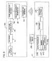
- FIG. 8is a block diagram showing the components of a circuit for using the electrical signal generated by the device of FIGS. 6 or 7 ;
- FIG. 9a detailed circuit diagram of the circuit in FIG. 8 ;
- FIGS. 10a-cshow the electrical signal generated by the actuator, the rectified electrical signal and the regulated electrical signal respectively;
- FIG. 11is a plan view of a tuned loop antenna of FIG. 8 illustrating the jumper at a position maximizing the inductor cross-section;
- FIG. 12is a plan view of the tuned loop antenna of FIG. 8 illustrating the jumper at a position minimizing the inductor cross-section;
- FIG 13is an elevation view of a preferred deflector assembly and casing which enclose the actuator of the present invention
- FIG 14is an elevation view of an alternate embodiment a deflector assembly using a sliding paddle
- FIGS. 15a-care elevational cross-sections taken along line 15-15 of FIG. 13 showing the preferred embodiment of a casing and deflector assembly using a quick release mechanism
- FIGS. 16a-dare elevational cross-sections taken along line 16-16 of FIG. 14 .
- Piezoelectric and electrostrictive materialsdevelop a polarized electric field when placed under stress or strain.
- the electric field developed by a piezoelectric or electrostrictive materialis a function of the applied force causing the mechanical stress or strain.
- electroactive devicesundergo dimensional changes in an applied electric field.
- the dimensional change (i.e., expansion or contraction) of an electroactive deviceis a function of the applied electric field.
- Electroactive devicesare commonly used as drivers, or “actuators” due to their propensity to deform under such electric fields. These electroactive devices or actuators also have varying capacities to generate an electric field in response to a deformation caused by an applied force.
- Electroactive devicesinclude direct and indirect mode actuators, which typically make use of a change in the dimensions of the material to achieve a displacement, but in the present invention are preferably used as electromechanical generators.
- Direct mode actuatorstypically include a piezoelectric or electrostrictive ceramic plate (or stack of plates) sandwiched between a pair of electrodes formed on its major surfaces. The devices generally have a sufficiently large piezoelectric and/or electrostrictive coefficient to produce the desired strain in the ceramic plate.
- direct mode actuatorssuffer from the disadvantage of only being able to achieve a very small displacement (strain), which is, at best, only a few tenths of a percent.
- direct mode generator-actuatorsrequire application of a high amount of force to piezoelectrically generate a pulsed momentary electrical signal of sufficient magnitude to activate a latching relay.
- Indirect mode actuatorsare known to exhibit greater displacement and strain than is achievable with direct mode actuators by achieving strain amplification via external structures.
- An example of an indirect mode actuatoris a flextensional transducer.
- Flextensional transducersare composite structures composed of a piezoelectric ceramic element and a metallic shell, stressed plastic, fiberglass, or similar structures. The actuator movement of conventional flextensional devices commonly occurs as a result of expansion in the piezoelectric material which mechanically couples to an amplified contraction of the device in the transverse direction. In operation, they can exhibit several orders of magnitude greater strain and displacement than can be produced by direct mode actuators.
- a typical unimorphis a concave structure composed of a single piezoelectric element externally bonded to a flexible metal foil, and which results in axial buckling or deflection when electrically energized. Common unimorphs can exhibit a strain of as high as 10%.
- a conventional bimorph deviceincludes an intermediate flexible metal foil sandwiched between two piezoelectric elements. Electrodes are bonded to each of the major surface of the ceramic elements and the metal foil is bonded to the inner two electrodes. Bimorphs exhibit more displacement than comparable unimorphs because under the applied voltage, one ceramic element will contract while the other expands. Bimorphs can exhibit strains up to 20%.
- asymmetrically stress biased electroactive deviceshave been proposed in order to increase the axial deformation of the electroactive material, and therefore increase the achievable strain of the electroactive material.
- the asymmetric stress biasingproduces a curved structure, typically having two major surfaces, one of which is concave and the other which is convex.
- THUNDERA unimorph actuator called "THUNDER”, which has improved displacement, strain and load capabilities, has recently been developed and is disclosed in U.S. patent no. 5,632,841 .
- THUNDER(which is an acronym for THin layer composite UNimorph ferroelectric Driver and sEnsoR), is a unimorph actuator in which a pre-stress layer is bonded to a thin piezoelectric ceramic wafer at high temperature, and during the cooling down of the composite structure asymmetrically stress biases the ceramic wafer due to the difference in thermal contraction rates of the pre-stress layer and the ceramic layer.
- the THUNDER actuator 12is as a composite structure, the construction of which is illustrated in FIG. 1 .
- Each THUNDER actuator 12is constructed with an electroactive member preferably comprising a piezoelectric ceramic layer 67 of PZT which is electroplated 65 and 65a on its two opposing faces.
- a pre-stress layer 64preferably comprising spring steel, stainless steel, beryllium alloy or other metal substrate, is adhered to the electroplated 65 surface on one side of the ceramic layer 67 by a first adhesive layer 66.
- the adhesive layer 66acts as a prestress layer.
- the first adhesive layer 66is preferably LaRCTM-SI material, as developed by NASA-Langley Research Center and disclosed in U.S. Pat. No. 5,639,850 .
- a second adhesive layer 66ais adhered to the opposite side of the ceramic layer 67.
- the ceramic layer 67, the adhesive layer(s) 66 and 66a and the pre-stress layer 64are simultaneously heated to a temperature above the melting point of the adhesive material.
- the various layers composing the THUNDER actuatornamely the ceramic layer 67, the adhesive layers 66 and 66a and the pre-stress layer 64
- the various layers composing the THUNDER actuatornamely the ceramic layer 67, the adhesive layers 66 and 66a and the pre-stress layer 64
- the various layers composing the THUNDER actuatorare typically placed inside of an autoclave or a convection oven as a composite structure, and slowly heated by convection until all the layers of the structure reach a temperature which is above the melting point of the adhesive 66 material but below the Curie temperature of the ceramic layer 67.
- the ceramic layer 67It is desirable to keep the temperature of the ceramic layer 67 beneath the Curie temperature of the ceramic layer in order to avoid disrupting the piezoelectric characteristics of the ceramic layer 67. Because the multi-layer structure is typically convectively heated at a slow rate, all of the layers tend to be at approximately the same temperature. In any event, because an adhesive layer 66 is typically located between two other layers (i.e. between the ceramic layer 67 and the pre-stress layer 64), the ceramic layer 67 and the pre-stress layer 64 are usually very close to the same temperature and are at least as hot as the adhesive layers 66 and 66a during the heating step of the process. The THUNDER actuator 12 is then allowed to cool.
- the ceramic layer 67becomes compressively stressed by the adhesive layers 66 and 66a and pre-stress layer 64 due to the higher coefficient of thermal contraction of the materials of the adhesive layers 66 and 66a and the pre-stress layer 64 than for the material of the ceramic layer 67. Also, due to the greater thermal contraction of the laminate materials (e.g. the first pre-stress layer 64 and the first adhesive layer 66) on one side of the ceramic layer 67 relative to the thermal contraction of the laminate material(s) (e.g. the second adhesive layer 66a) on the other side of the ceramic layer 67, the ceramic layer deforms in an arcuate shape having a normally convex face 12a and a normally concave face 12c, as illustrated in FIGS. 1 and 2 .
- the laminate materialse.g. the first pre-stress layer 64 and the first adhesive layer 66
- the ceramic layerdeforms in an arcuate shape having a normally convex face 12a and a normally concave face 12c, as illustrated in FIGS.
- One or more additional pre-stressing layer(s)may be similarly adhered to either or both sides of the ceramic layer 67 in order, for example, to increase the stress in the ceramic layer 67 or to strengthen the actuator 12B.
- a second prestress layer 68is placed on the concave face 12a of the actuator 12B having the second adhesive layer 66a and is similarly heated and cooled.
- the second prestress layer 68comprises a layer of conductive metal. More preferably the second prestress layer 68 comprises a thin foil (relatively thinner than the first prestress layer 64) comprising aluminum or other conductive metal.
- the ceramic layer 67similarly becomes compressively stressed by the adhesive layers 66 and 66a and pre-stress layers 64 and 68 due to the higher coefficient of thermal contraction of the materials of the adhesive layers 66 and 66a and the pre-stress layers 64 and 68 than for the material of the ceramic layer 67. Also, due to the greater thermal contraction of the laminate materials (e.g. the first pre-stress layer 64 and the first adhesive layer 66) on one side of the ceramic layer 67 relative to the thermal contraction of the laminate material(s) (e.g.
- the ceramic layer 67deforms into an arcuate shape having a normally convex face 12a and a normally concave face 12c, as illustrated in FIG. 1a .
- the substrate comprising a separate prestress layer 64may be eliminated and the adhesive layers 66 and 66a alone or in conjunction may apply the prestress to the ceramic layer 67.
- the prestress layer(s) 64 and 68 and the adhesive layer(s) 66 and 66amay be heated and bonded to a ceramic layer 67, while the ceramic layer 67 is at a lower temperature, in order to induce greater compressive stress into the ceramic layer 67 when cooling the actuator 12.
- Yet another alternate actuator 12Dincludes a composite piezoelectric ceramic layer 69 that comprises multiple thin layers 69a and 69b of PZT which are bonded to each other.
- Each thin layer 69a and 69bis electroplated 65 and 65a, and 65b and 65c on each major face respectively.
- the individual layers 69a and 69bare then bonded to each other with an adhesive layer 66b, using an adhesive such as LaRC-SI.
- the thin layers 69a and 69bmay be bonded to each other by cofiring the thin sheets of piezoelectric material together. As few as two layers 69a and 69b, but preferably at least four thin sheets of piezoelectric material may be bonded/cofired together.
- the composite piezoelectric ceramic layer 69may then be bonded to prestress layer(s) 64 with the adhesive layer(s) 66 and 66a, and heated and cooled as described above to make a modified THUNDER actuator 12D.
- the composite ceramic layerBy having multiple thinner layers 69a and 69b of piezoelectric material in a modified actuator 12D, the composite ceramic layer generates a lower voltage and higher current as compared to the high voltage and low current generated by a THUNDER actuator 12 having only a single thicker ceramic layer 67.
- a flexible insulatormay be used to coat the convex face 12a of the actuator 12.
- This insulative coatinghelps prevent unintentional discharge of the piezoelectric element through inadvertent contact with another conductor, liquid or human contact.
- the coatingalso makes the ceramic element more durable and resistant to cracking or damage from impact.
- the adhesive layer 67a on the convex face 12a of the actuator 12may act as the insulative layer.
- the insulative layermay comprise a plastic, TEFLON or other durable coating.
- Electrical energymay be recovered from or introduced to the actuator element 12 by a pair of electrical wires 14.
- Each electrical wire 14is attached at one end to opposite sides of the actuator element 12.
- the wires 14may be connected (for example by glue or solder 20) directly to the electroplated 65 and 65a faces of the ceramic layer 67, or they may alternatively be connected to the pre-stress layer(s) 64.
- the pre-stress layer 64is preferably adhered to the ceramic layer 67 by LaRC-SI material, which is a dielectric.
- each electrical wire 14is preferably connected to an electric pulse modification circuit 10.
- Prestressed flextensional transducers 12are desirable due to their durability and their relatively large displacement, and concomitant relatively high voltage that such transducers are capable of developing.
- the present inventionmay be practiced with any electroactive element having the properties and characteristics herein described, i.e., the ability to generate a voltage in response to a deformation of the device.
- the inventionmay be practiced using magnetostrictive or ferroelectric devices.
- the transducersalso need not be normally arcuate, but may also include transducers that are normally flat, and may further include stacked piezoelectric elements.
- the forcedeforms the piezoelectric element 67.
- the forcemay be applied to the piezoelectric actuator 12 by any appropriate means such as by application of manual pressure directly to the piezoelectric actuator, or by other mechanical means.
- the forceis applied by a mechanical switch (e.g., a plunger, striker, toggle or roller switch) capable of developing a mechanical impulse for application to and removal from the actuator 12.
- the mechanical impulse(or removal thereof) is of sufficient force to cause the actuator 12 to deform quickly and accelerate over a distance (approximately 10 mm) which generates an electrical signal of sufficient magnitude to activate an electromechanical latching relay.
- FIGS. 3, 4 and 5which do not form part of the invention:
- An illustration of prior means generating an electrical pulse by application of mechanical forcecomprises a switch plate 18 and a plunger assembly 13.
- the two ends of the piezoelectric actuatorare each pivotably held in place within a recess 44 of a switch plate 18.
- the switch plate 18is the same shape as the actuator 12 contained therein, preferably rectangular.
- a circular actuatoris mounted in a circular recess of a circular switch plate.
- the recess(es) 44 in the switch plate 18hold the actuator 12 in place in its relaxed, i.e., undeformed state.
- the recesses 44are also sufficiently deep to fully receive the ends or edges of the actuator 12 in its fully deformed, i.e., flat state.
- the plunger assemblycomprises a push button 22 pivotably connected to a hinged quick-release mechanism 24.
- the opposite end of the quick-release mechanism 24contacts shaft 26 connected to a pair of plates 27 and 28 which are clamped on both sides of the actuator 12.
- a release cog 25is located along the path of the quick-release mechanism 24.
- the quick-release mechanism 24pushes down on the shaft 26 and plates 27 and 28 and deforms the actuator 12.
- the quick-release mechanism 24pivots on its hinge and releases the downward pressure from the shaft 26, plates 27 and 28 and actuator 12.
- the actuatoron account of the restoring force of the substrate of the prestress layer 64, returns quickly to its undeformed state in the direction of arrow 30 as in FIG. 5 .
- the applied forcecauses the piezoelectric actuator 12 to deform.
- the deformation of the piezoelectric element 67generates an instantaneous voltage between the faces 12a and 12c of the actuator 12, which produces a pulse of electrical energy.
- the actuator 12recovers its original arcuate shape. This is because the substrate or prestress layers 64 and 68 to which the ceramic 67 is bonded exert a compressive force on the ceramic 67, and the actuator 12 thus has a coefficient of elasticity that causes the actuator 12 to return to its undeformed neutral state. On the recovery stroke of the actuator 12, the ceramic 67 returns to its undeformed state and thereby produces another electrical pulse of opposite polarity.
- the downward (applied) or upward (recovery) strokesshould cause a force over a distance that is of sufficient magnitude to create the desired electrical pulse.
- the duration of the recovery stroke, and therefore the duration of the pulse producedis preferably in the range of 50-100 milliseconds, depending on the amount of force applied to the actuator 12.
- the actuator 12is clamped at one end 121 and the mechanical impulse is applied to the edge on the free end 122, i.e., at the end opposite to the clamped end 121 of the actuator 12.
- the electrical pulse that is generated upon removal of the forceis an oscillating wave rather than a single pulse as in the prior actuating means disclosed above.
- FIG. 6illustrates one embodiment of a device for generating an electrical pulse by application of mechanical force to an end of the actuator 12.
- This devicecomprises an actuator 12 mounted between a base plate 70 and a clamping member 75 as well as a deflector assembly 72.
- the base plate 70is preferably of substantially the same shape (in plan view) as the actuator 12 attached thereon, and most preferably rectangular.
- One end 121 of the piezoelectric actuator 12is held in place between the clamping member 75 and the upper surface 70a of a base plate 70, preferably on one end thereof.
- the clamping member 75comprises a plate or block having a lower surface 75a designed to mate with the upper surface 70a of the base plate 70 with the actuator 12 therebetween.
- the devicealso has means for urging 76 the mating surface 75a of the clamping block towards the upper surface 70a of the base plate 70.
- the means for urging 76 together the mating surfaces 70a and 75a of the base plate 70 and clamping plate 75may comprise screws, clamping jaws or springs or the like.
- the urging means 76comprises at least one screw 76 passing through the clamping member 75 and into a screw hole 77 in the upper surface 70a of the base plate 70.
- One end 121 of an actuator 12is placed between the mating surfaces 70a and 75a of the base and clamping plates 70 and 75.
- the mating surfaces 70a and 75aare then urged towards each other with the screw 76 to rigidly hold the end 121 of the actuator 12 in place between the base and clamping plates 70 and 75 with the opposite end 122 of the actuator 12 free to be moved by a mechanical impulse applied manually or preferably by a deflector assembly 72.
- the surfaces 70a and 75a of the base and clamping plate 70 and 75are designed to best distribute pressure evenly along the end 121 of the actuator therebetween.
- the upper surface 70a of the base plate 70 contacting the end 121 of the actuatoris preferably substantially flat and lower surface 75a of the clamping member 75 preferably has a recess 74 therein which accommodates insertion of the actuator end 121 therein.
- the depth of the recess 74is equal to half the thickness of the actuator substrate 64, but may be as deep as the substrate thickness.
- the end 121 of the actuator 12may be placed between the recess 74 and the upper surface 70a of the base plate 70 and secured therebetween by the screw 76.
- either or both of the mating surfaces 70a and 75a of the base and clamping plates 70 and 75may have a recess therein to accommodate insertion and retention of the end 121 of the actuator 12 therebetween.
- the portion of the bottom surface 75a of the clamping member 75 beyond the recess 74has no contact with the actuator 12, and is that portion through which the screw 76 passes.
- This portion of the bottom surface 75amay contact the upper surface 70a of the base plate 70, but most preferably there is a small gap (equal to the difference of the substrate thickness and the recess depth) between the lower surface 75a of the clamping member 75 and the top surface 70a of the base plate 70 when the actuator 12 is inserted therebetween.
- the mating surfaces 70a and 75a of the base and clamping plates 70 and 75may be adhesively bonded together (rather than screwed) with the end 121 of the actuator 12 sandwiched therebetween.
- the clamping member 75 and base plate 70may comprise a single molded structure having a central slot into which may be inserted one end 121 of the actuator 12.
- the clamping assembly 75holds the actuator 12 in place in its relaxed, i.e., undeformed state above the base plate 70 with the free end 122 of the actuator 12 in close proximity to a deflector 72 assembly. More specifically, the actuator 12 is preferably clamped between the mating surfaces 70a and 75a of the base and clamping plates 70 and 75 with the convex face 12a of the actuator 12 facing the base plate 70. Since the actuator 12 in its relaxed state is arcuate, the convex face 12a of the actuator 12 curves away from the upper surface 70a of the base plate 70 while approaching the free end 122 of the actuator 12. Mechanical force may then be applied to the free end 122 of the actuator 12 in order to deform the electroactive element 67 to develop an electrical signal.
- the actuator 12Because of the composite, multi-layer construction of the actuator 12 it is important to ensure that the clamping member 75 not only holds the actuator 12 rigidly in place, but also that the actuator 12 is not damaged by the clamping member 75.
- the actuator 12, and more specifically the ceramic layer 67should not be damaged by the clamping action of the clamping member 75 in a static mode, but especially in the dynamic state when applying a mechanical impulse to the actuator 12 with the plunger 72.
- the bottom corner of the ceramiccontacts the base plate 70 and is further pushed into the base plate, which may crack or otherwise damage the ceramic layer 67.
- the switch plate 70has a recessed area 80° in its upper surface 70a which not only protects the electroactive element 67 from damage but also provides electrical contact to the convex face 12a of the actuator 12 so that the electrical signal developed by the actuator 12 may be applied to downstream circuit elements.
- one end 121 of the actuatoris placed between the surfaces 75a and 70a of the clamping and base plates 75 and 70 such that only the substrate 64 contacts both surface 75a and 70a.
- the clamping plate 75preferably contacts the concave surface 12b of the actuator 12 along the substrate 64 up to approximately the edge of the ceramic layer 67 on the opposite face 12a of the actuator 12.
- the clamping membermay however extend along the convex face 12c further than the edge C of the ceramic layer 67 in order to apply greater or more even pressure to the actuator surfaces 12a and 12c between the clamping member 75 and base plate 70.
- the ceramic layer 67which extends above the surface of the substrate 64 on the convex face 12a extends into the recessed area 80 of the switch plate 70. This prevents the ceramic layer 67 from contacting the upper surface 70a of the base plate 70, thereby reducing potential for damage to the ceramic layer 67.
- the recess 80is designed not only to prevent damage to the ceramic layer 67, but also to provide a surface along which electrical contact can be maintained with the electrode 68 on the convex face of the actuator 12.
- the recess 80extends into the base plate 70 and has a variable depth, preferably being angled to accommodate the angle at which the convex face 12a of the actuator 12 rises from the recess 80 and above the top surface 70a of the base plate 70. More specifically, the recess 80 preferably has a deep end 81 and a shallow end 82 with its maximum depth at the deep end 81 beneath the clamping member 75 and substrate 12 just before where the ceramic layer 67 extends into the recess 80 at point C. The recess 80 then becomes shallower in the direction approaching the free end 122 of the actuator 12 until it reaches its minimum depth at the shallow end 82.
- the recess 80preferably contains a layer of rubber 85 along its lower surface which helps prevent the ceramic layer 67 from being damaged when the actuator 12 is deformed and the lower edge C of the ceramic layer 67 is pushed into the recess 80.
- the rubber layer 85is of substantially uniform thickness along its length, the thickness of the rubber layer 85 being substantially equal to the depth of the recess 80 at the shallow end 82.
- the length of the rubber layer 85is preferably slightly shorter than the length of the recess 80 to accommodate the deformation of the rubber layer 85 when the actuator 12 is pushed into the recess and rubber layer 85.
- the rubber layer 85preferably has a flexible electrode layer 90 overlying it to facilitate electrical contact with the aluminum layer 68 on the ceramic layer 67 on the convex face 12a of the actuator 12. More preferably, the electrode layer 90 comprises a layer of copper overlaying a layer of KAPTON film, as manufactured by E.I. du Pont de Nemours and Company, bonded to the rubber layer 85 with a layer of adhesive, preferably CIBA adhesive.
- the electrode layer 90preferably extends completely across the rubber layer 85 from the deep end 81 to the shallow end 82 of the recess 80 and continues for a short distance on the top surface 70a of the base plate 70 beyond the recess 80.
- the end 121 of the actuator 12is not only secured between the clamping plate 75 and the base plate 70, but the aluminum electrode layer 68 covering the ceramic layer 67 of the actuator 12 is in constant contact with the electrode layer 90 in the recess 80 at all times, regardless of the position of the actuator 12 in its complete range of motion.
- the depth of the recess 80is at least equal to a preferably slightly less than the thickness of the laminate layers (adhesive layers 66, ceramic layer 67 and prestress layer 68) extending into the recess 80.
- An 8-mil thick layer of PZT-5A in a 1.5 inch squarewas centered on the adhesive layer.
- a 1-mil thick layer of adhesive (with no metal filler)was placed in a 1.47 inch square centered on the PZT layer.
- a 1-mil thick layer of aluminum in a 1.46 inch squarewas centered on the adhesive layer.
- the tab 121 of the actuatorwas placed in a recess in a clamping block 76 having a length of 0.375 inch and a depth of 4 mils.
- the base plate 70had a 0.26 in long recess 80 where the deep end 81 of the recess had a depth of 20 mils and tapered evenly to a depth of 15 mils at the shallow end 82 of the recess 80.
- a rubber layer 85having a thickness of 15 mils and a length of .24 inches was placed in the recess 80.
- An electrode layer of 1 mil copper foil overlying 1 mil KAPTON tapewas adhered to the rubber layer and extended beyond the recess 1.115 inches.
- the clamping member 75was secured to the base plate 70 with a screw 76 and the aluminum second prestress layer of the actuator 12 contacted the electrode 90 in the recess 80 substantially tangentially (nearly parallel) to the angle the actuator 12 thereby maximizing the surface area of the electrical contact between the two.
- a weight 95may be attached to the free end 122 of the actuator 12.
- the actuator 12is capable of developing more electrical energy from its oscillation than an actuator 12 having no additional mass at its free end 122.
- FIGS. 6 and 7it is desirable to generate an electrical signal by deforming the actuator 12.
- Deformation of the actuator 12may be accomplished by any suitable means such as manually or by mechanical deflection means such as a plunger, lever or the like.
- a simple deflector 72is mounted to the base plate 70 in proximity to the free end 122 of the actuator 12.
- This deflector assembly 72includes a lever 86 having first and second ends 87 and 88. The lever is pivotably mounted between the two ends 87 and 88 to a fulcrum 89.
- the lever 86By exerting a force on the first end 87 of the lever 86 in the direction of arrow 91, the lever pivots about the fulcrum 89 and applies a mechanical impulse in the direction of arrow 81 to the free end 122 of the actuator 12.
- the lever 86may be moved opposite the direction of arrow 91 and the actuator 12 may thus be deflected in the direction opposite arrow 81.
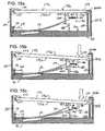
- FIGS. 13 and 15a-cshow the preferred embodiment of a casing with a deflector assembly 72 and containing the actuator 12.
- the base plate 70forms the base of a casing 200, which encloses the actuator 12.
- On each side of the casing 200is a wall 201, 202, 203 and 204 which extends perpendicularly from the top surface 70a of the base plate 70.
- On one end of the casing 200is mounted a deflector assembly 72.
- the plungerhas an interior surface 172b and an exterior surface 172a, as well as a free end 173 and a mounted end 174.
- the plunger 172is pivotably mounted on one end 174 to a wall 201 of the casing 200.
- the free end 173 of the plunger 172has a ridge 173a thereon which engages a lip 202a on the opposite wall 202 of the casing.
- the free end 173 of the plunger 172is spring loaded so that the ridge 173a is constantly urged towards the lip 202a.
- an actuator 12 mounted on a base plate 70is contained within a casing 200 formed by the base plate 70 and four walls 201, 202, 203 and 204 as well as a plunger 172 pivotably mounted opposite the base plate 70 on a wall 201 of the casing 200. Because the plunger is pivotably mounted, placing pressure (in the direction of arrow 180 on the on the exterior surface 172a of the plunger 172 makes it pivot about the hinge 175 toward the top surface 70a of the base plate 70. Because the plunger is pivotably mounted and spring loaded, releasing pressure from the on the exterior surface 172a of the plunger 172 makes it pivot about the hinge 175 away the top surface of the base plate 70 until the ridge 173a catches on the lip 202a.
- a mounted quick release mechanism 180comprising a spring loaded rocker arm 185 on the interior surface 172b of the plunger 172 which works in conjunction with a release pin 186 mounted on the top surface 70 of the base plate 70.
- the quick release mechanism 180is designed to deflect and then quickly release the free end 122 of the actuator 12 in order to allow it to vibrate between positions 291 and 292.
- the quick release mechanism 180is also designed not to interfere with the vibration of the actuator 12 as well as to return to a neutral position for follow-on deflections of the actuator 12.
- the rocker arm 185is pivotably attached to the interior surface 172b of the plunger 172 above the free end 122 of the actuator 12. More specifically, the rocker arm 185 is pivotably attached in such a way that it has a neutral position from which it may pivot away from the clamped end 121 of the actuator, but will not pivot towards the clamped end 121 of the actuator 12 from that neutral position.
- a rotational stop 183forms part of the quick release mechanism 180 and its placement prevents the rocker arm from pivoting beyond the neutral position at the stop 183.
- the rocker arm 185is preferably spring loaded in order to keep the rocker arm 185 in its neutral position when not being deflected. To this end a spring 187 in compression is placed on the side of the rocker arm 185 opposite the stop 183, between the rocker arm 185 and a spring stop 188.
- a release pin 186which is located on the top surface 70a of the base plate 70.
- the release pin 186is located in a position just beyond the free end 122 of the actuator 12 in its deflected position, but not beyond the rocker arm 185.
- the release pin 186will contact the rocker arm 185 but not the actuator 12.
- the release pin 186pushes the rocker arm 185 away, making the rocker arm 185 pivot away from the clamped end 121 of the actuator 12.
- the rocker arm 185pivots until the edge 122 of the actuator 12 is no longer held by the rocker arm 185 in position 292, at which point the edge 122 of the actuator 12 is released and springs back to its undeformed state, thereby oscillating between positions 291 and 292.
- the plunger 172When pressure from the plunger 172 is released, the plunger 172 returns to its undeflected position (with the ridge 173a against the lip 202a) by virtue of the restoring force of the spring 150. Also when the pressure from the plunger 172 is released, and the plunger 172 returns to its undeflected position, the rocker arm 185 also returns to its undeflected position (above the actuator 12 against the stop 183) by virtue of the restoring force of the spring 187. Lastly, the actuator 12 also returns to its undeflected state in position 291 after its oscillations between positions 291 and 292 have ceased.
- FIGS. 14 and 16a-dshow an alternate embodiment of a deflector assembly 72 mounted to a casing 200 that contains the actuator 12.
- the base plate 70forms the base of a casing 200, which encloses the actuator 12.
- On each side of the casing 200is a wall 201, 202, 203 and 204 which extends perpendicularly from the top surface 70a of the base plate 70.
- Attached to the top of the walls of the casing 200 (opposite the base plate 70)is a face plate 220 to which is mounted a slide mechanism 230 that acts as a deflector assembly 72.
- the face plate 220has an interior surface 220a and an exterior surface 220b and a channel 240 extending through substantially the center of the face plate 220.
- the channel 240has a first end 241 and a second end 242 and extends substantially linearly along an axis L perpendicular to the first and second walls 201 and 202 of the casing 200.
- the first end 241 of the channel 240 through the face plate 220is in proximity to the first wall 201 of the casing 200 and the second end 242 of the channel 240 through the face plate 220 is in proximity to the second wall 202 of the casing 200.
- the second end of the channel 240preferably extends further towards the second wall 202 of the casing than does the free end 122 of the actuator 12.
- the channel 240is adapted to slidably retain a spring loaded paddle 250.
- the paddlehas first and second ends 251 and 252 respectively and a central pin 255.
- the channel in the face plate 220allows the paddle to extend through the face plate 220, while also slidably retaining the central pin 255 in the channel 240.
- the paddle 250extends through the face plate 220 by means of the channel 240, along which the paddle may be slid in a direction parallel to the channels' axis L, i.e., from the clamped end 121 to the free end 122 of the actuator 12 and back.
- the first end 251 of the paddle 250is located above the exterior surface 220b of the face plate 220 and the second end 252 of the paddle 250 is located within the casing 200 above the actuator 12.
- the paddle 250is retained in the described position be means of the pin 255 which is retained in the channel 240.
- the width of the channel 240 at the exterior surface 220bis sufficient for the paddle upper portion 251 to pass through, as is the width of the channel 240 at the interior surface 220a is sufficient for the paddle lower portion 252 to pass through.
- the width and height of the channel 240 within the face plate 220(between the interior and exterior surfaces 220a and 220b) is sufficient to accommodate the width and height of the central pin 255, which is wider than the width of the paddle upper and lower portions 251 and 252.
- the first end 251 of the paddle 250preferably extends a distance above the exterior surface 220b of the face plate 220 enough to be grasped manually.
- the second end 252 of the paddle 250preferably extends into the casing 200 a distance above the actuator 12 such that the paddle 250 does not contact the clamping member 75 and/or clamped end 121 of the actuator 12, but also far enough that it may contact and deflect the free end 122 of the actuator 12.
- the paddle 250is also preferably hinged at the second end 252 (within the casing 200 or the channel 240 at or in proximity to the central pin 255) in a manner that allows the second end 252 to pivot about the hinge or central pin 255 when travelling in one direction but not the other.
- the second end 252 of the paddle 250is hinged in a way that it may pivot when the paddle 250 is travelling toward the first wall 201 of the casing 200 but not pivot when travelling towards the second wall 202 of the casing 200.
- the paddle 250is also spring loaded so that the paddle is constantly urged along the channel 240 towards the first wall 201 of the casing 200.
- a spring 260held between the paddle and the first 201 or second wall 202 of the casing 200 or most preferably the spring 260 held between the paddle 250 and the first or second end 241 or 242 of the channel 240.
- the spring 260is either held in tension between the paddle 250 and the first end 241 of the channel 240, or most preferably the spring 260 is held in compression between the paddle 250 and the second end 242 of the channel 240.
- an actuator 12 mounted on a base plate 70is contained within a casing 200 formed by the base plate 70, four walls 201, 202, 203 and 204 and a face plate opposite the base plate 70. Because the paddle 250 is slidably mounted, placing pressure (in the direction of arrow 281 on the on the 251 first end of the paddle makes it slide along the channel 240 toward the second wall 202 of the casing 200. Because the paddle 250 is slidably mounted and spring loaded, releasing pressure from the paddle 250 makes it return along the channel 240 toward the first wall 201 of the casing 200 until it comes to rest against the first end 241 of the channel 240.
- the paddle upper portion 251is pivotably attached to the paddle lower portion 252 below the interior surface 220a of the face plate 220 (within the casing 200) above the actuator 12. More specifically, the paddle lower portion 252 is pivotably attached in such a way that it has a neutral position from which it may pivot away from the clamped end 121 of the actuator, but will not pivot towards the clamped end 121 of the actuator 12 from that neutral position. In other words the shape of the paddle 250 prevents the lower portion 252 from pivoting beyond the neutral position.
- the paddle lower portion 252contacts concave face 12c of the actuator 12 and commences to deflect the actuator free end 122 (away from position 291).
- the paddle lower portion 252depresses the free end 122 of the actuator 12 to its maximum deflection at position 292 when the free end 122 is directly beneath the paddle lower portion 252.
- the free end 122 of the actuator 12is abruptly released from the applied deflection of the paddle lower portion 252.
- the edge 122 of the actuator 12springs back to its undeformed state at position 291, thereby oscillating between positions 291 and 292.
- the paddleUpon release of pressure (in the direction of arrow 281) from the paddle 250, the paddle then travels in the direction of arrow 282, by virtue of the restoring force of the spring 260.
- the free end 122 of the actuator 12 in position 291applies pressure against the lower portion 252 of the paddle 250.
- the lower portion 252pivots about the hinged central pin 255 of the paddle.
- the lower portion 252After the paddle lower portion 252 has traveled in the direction of arrow 282 beyond the free end 122 of the actuator, the lower portion 252 returns to its undeflected (unbent) state. The pivoting of the paddle lower portion 252 allows the paddle 250 to return to its neutral undeflected position at the first end 241 of the channel 240.
- the end 122 of the actuator 12When the end 122 of the actuator 12 is deflected and then released (either manually or using a deflector assembly 72 such as in figures 6-7 , or 13-16 ), the end 122 of the actuator 12, much like a diving board, oscillates back and forth between positions 291 and 292. This is because the substrate and prestress layer 64 and 68 to which the ceramic 67 is bonded exert a compressive force on the ceramic 67 thereby providing a restoring force. Therefore, the actuator 12 has a coefficient of elasticity or spring constant that causes the actuator 12 to return to its undeformed neutral state at position 291. The oscillation of the actuator 12 has the waveform of a damped harmonic oscillation, as is illustrated in FIG. 10a .
- the amplitude of the oscillation of the free end 122 of the actuator 12is at its maximum immediately following (within a few oscillations after) the release of the mechanical impulse from the free end 122 of the actuator 12.
- the amplitudegradually decreases over time (approximately exponentially) until the actuator 12 is at rest in its neutral position.
- the applied forcewhether by manual or other mechanical deflection means 72 causes the piezoelectric actuator 12 to deform and by virtue of the piezoelectric effect, the deformation of the piezoelectric element 67 generates an instantaneous voltage between the faces 12a and 12c of the actuator 12, which produces an electrical signal.
- the actuatoroscillates between positions 291 and 292 until it gradually returns to its original shape.
- the ceramic layer 67strains, becoming alternately more compressed and less compressed.
- the polarity of the voltage produced by the ceramic layer 67depends on the direction of the strain, and therefore, the polarity of the voltage generated in compression is opposite to the polarity of the voltage generated in tension.
- the voltage produced by the ceramic element 67oscillates between a positive and negative voltage for a duration of time.
- the duration of the oscillation, and therefore the duration of the oscillating electrical signal producedis preferably in the range of 100-250 milliseconds, depending on the shape, mounting and amount of force applied to the actuator 12.
- the electrical signal generated by the actuator 12is applied to downstream circuit elements via wires 14 connected to the actuator 12. More specifically, a first wire 14 is connected to the electrode 90 which extends into the recess 80 and contacts the electrode 68 on the convex face 12a of the actuator 12. Preferably the wire 14 is connected to the electrode 90 outside of the recess close to the end of the base plate 70 opposite the end having the clamping member 75. A second wire 14 is connected directly to the first prestress layer 64, i.e., the substrate 64 which acts as an electrode on the concave face 12c of the actuator 12.
- the actuator 12is connected to circuit components downstream in order to generate an RF signal for actuation of a switch initiator.
- circuit componentsinclude a rectifier 31, a voltage regulator U2, an encoder 40 (preferably comprising a peripheral interface controller (PIC) chip) as well as an RF generator 50 and antenna 60.
- FIG. 10bshows the waveform of the electrical signal of FIG 10a after it has been rectified.
- FIG. 10cshows the waveform of the rectified electrical signal of FIG 10b after it has been regulated to a substantially uniform voltage, preferably 3.3 VDC.
- the actuator 12is first connected to a rectifier 31.
- the rectifier 31comprises a bridge rectifier 31 comprising four diodes D1, D2, D3 and D4 arranged to only allow positive voltages to pass.
- the first two diodes D1 and D2are connected in series, i.e., the anode of D1 connected to the cathode of D2.
- the second two diodes D3 and D4are connected in series, i.e., the anode of D3 connected to the cathode of D4.
- the anodes of diodes D2 and D4are connected, and the cathodes of diodes D1 and D3 are connected, thereby forming a bridge rectifier.
- the rectifieris positively biased toward the D2-D4 junction and negatively biased toward the D1-D3 junction.
- One of the wires 14 of the actuator 12is electrically connected between the junction of diodes D1 and D2, whereas the other wire 14 (connected to the opposite face of the actuator 12) is connected to the junction of diodes D3 and D4.
- the junction of diodes D1 and D3are connected to ground.
- a capacitor C11is preferably connected on one side to the D2-D4 junction and on the other side of the capacitor C11 to the D1-D3 junction in order to isolate the voltages at each side of the rectifier from each other. Therefore, any negative voltages applied to the D1-D2 junction or the D3-D4 junction will pass through diodes D1 or D3 respectively to ground. Positive voltages applied to the D1-D2 junction or the D3-D4 junction will pass through diodes D2 or D4 respectively to the D2-D4 junction.
- the rectified waveformis shown in FIG. 10b .
- the circuitalso comprises a voltage regulator U2, which controls magnitude of the input electrical signal downstream of the rectifier 31.
- the rectifier 31is electrically connected to a voltage regulator U2 with the D2-D4 junction connected to the Vin pin of the voltage regulator U2 and with the D1-D3 junction connected to ground and the ground pin of the voltage regulator U2.
- the voltage regulator U2comprises for example a LT1121 chip voltage regulator U2 with a 3.3 volts DC output.
- the output voltage waveformis shown in FIG. 10c and comprises a substantially uniform voltage signal of 3.3 volts having a duration of approximately 100-250 milliseconds, depending on the load applied to the actuator 12..
- the regulated waveformis shown in FIG. 10b .
- the output voltage signal from the voltage regulatormay then be transmitted via another conductor to the relay switch 290, in order to change the position of a relay switch 290 from one position to another.
- the output voltageis connected through an encoder 40 to an RF generation section 50 of the circuit.
- the output of the voltage regulator U2is preferably used to power an encoder 40 or tone generator comprising a peripheral interface controller (PIC) microcontroller that generates a pulsed tone.
- PICperipheral interface controller
- This pulsed tonemodulates an RF generator section 50 which radiates an RF signal using a tuned loop antenna 60.
- the signal radiated by the loop antennais intercepted by an RF receiver 270 and a decoder 280 which generates a relay pulse to activate the relay 290.
- the output of the voltage regulator U2is connected to a PIC microcontroller, which acts as an encoder 40 for the electrical output signal of the regulator U2. More specifically, the output conductor for the output voltage signal (nominally 3.3 volts) is connected to the input pin of the programmable encoder 40.
- Types of register-based PIC microcontrollersinclude the eight-pin PIC12C5XX and PIC12C67x, baseline PIC16C5X, midrange PIC16CXX and the high-end PIC17CXX/PIC18CXX. These controllers employ a modified Harvard, RISC architecture that support various-width instruction words.
- the datapathsare 8 bits wide, and the instruction widths are 12 bits wide for the PIC16C5X/PIC12C5XX, 14 bits wide for the PIC12C67X/PIC16CXX, and 16 bits wide for the PIC17CXX/P1C18CXX.
- PICMICROSare available with one-time programmable EPROM, flash and mask ROM.
- the PIC17CXX/PIC18CXXsupport external memory.
- the encoder 40comprises for example a PIC model 12C671.
- the PIC12C6XX productsfeature a 14-bit instruction set, small package footprints, low operating voltage of 2.5 volts, interrupts handling, internal oscillator, on-board EEPROM data memory and a deeper stack.
- the PIC12C671is a CMOS microcontroller programmable with 35 single word instructions and contains 1024x14 words of program memory, and 128 bytes of user RAM with 10MHz maximum speed.
- the PIC12C671features an 8-level deep hardware stack, 2 digital timers (8-bit TMR0 and a Watchdog timer), and a four-channel, 8-bit A/D converter.
- the output of the PICmay include square, sine or saw waves or any of a variety of other programmable waveforms.
- the output of the encoder 40is a series of binary square waveforms (pulses) oscillating between 0 and a positive voltage, preferably +3.3 VDC.
- the duration of each pulse (pulse width)is determined by the programming of the encoder 40 and the duration of the complete waveform is determined by the duration of output voltage pulse of the voltage regulator U2.
- a capacitor C5is preferably be connected on one end to the output of the voltage regulator U2, and on the other end to ground to act as a filter between the voltage regulator U2 and the encoder 40.
- an ICas a tone generator or encoder 40 allows the encoder 40 to be programmed with a variety of values.
- the encoder 40is capable of generating one of many unique encoded signals by simply varying the programming for the output of the encoder 40. More specifically, the encoder 40 can generate one of a billion or more possible codes. It is also possible and desirable to have more than one encoder 40 included in the circuit in order to generate more than one code from one actuator or transmitter. Alternately, any combination of multiple actuators and multiple pulse modification subcircuits may be used together to generate a variety of unique encoded signals.
- the encoder 40may comprise one or more inverters forming a series circuit with a resistor and capacitor, the output of which is a square wave having a frequency determined by the RC constant of the encoder 40.
- the DC output of the voltage regulator U2 and the coded output of the encoder 40are connected to an RF generator 50.
- a capacitor C6may preferably be connected on one end to the output of the encoder 40, and on the other end to ground to act as a filter between the encoder 40 and the RF generator 50.
- the RF generator 50consists of tank circuit connected to the encoder 40 and voltage regulator U2 through both a bipolar junction transistor (BJT) Q1 and an RF choke. More specifically, the tank circuit consists of a resonant circuit comprising an inductor L2 and a capacitor C8 connected to each other at each of their respective ends (in parallel). Either the capacitor C8 or the inductor L2 or both may be tunable in order to adjust the frequency of the tank circuit.
- An inductor L1acts as an RF choke, with one end of the inductor L1 connected to the output of the voltage regulator U2 and the opposite end of the inductor L1 connected to a first junction of the L2-C8 tank circuit.
- the second and opposite junction of the L2-C8 tank circuitis connected to the collector of BJT Q1.
- the base of the BJT Q1is also connected through resistor R2 to the output side of the encoder 40.
- a capacitor C7is connected to the base of a BJT Q1 and to the first junction of the tank circuit.
- Another capacitor C9is connected in parallel with the collector and emitter of the BJT Q1. This capacitor C9 improves the feedback characteristics of the tank circuit.
- the emitter of the BJT Q1is connected through a resistor R3 to ground.
- the emitter of the BJT Q1is also connected to ground through capacitor C10 which is in parallel with the resistor R3.
- the capacitor C10 in parallel with the resistor R4provides a more stable conduction path from the emitter at high frequencies.
- the RF generator 50works in conjunction with a tuned loop antenna 60.
- the inductor L2 of the tank circuitserves as the loop antenna 60.
- the inductor/loop antenna L2comprises a single rectangular loop of copper wire having an additional smaller loop or jumper 61 connected to the rectangular loop L2. Adjustment of the shape and angle of the smaller loop 61 relative to the rectangular loop L2 is used to increase or decrease the apparent diameter of the inductor L2 and thus tunes the RF transmission frequency of the RF generator 50.
- a separate tuned antennamay be connected to the second junction of the tank circuit.
- the positive voltage output from the voltage regulator U2is connected the encoder 40 and the RF choke inductor L1.
- the voltagedrives the encoder 40 to generate a coded square wave output, which is connected to the base of the BJT Q1 through resistor R2.
- the coded square wave voltageis zero
- the base of the BJT Q1remains de-energized, and current does not flow through the inductor L1.
- the coded square wave voltageis positive
- the base of the BJT Q1is energized through resistor R2. With the base of the BJT Q1 energized, current is allowed to flow across the base from the collector to the emitter and current is also allowed to flow across the inductor L1.
- the square wavereturns to a zero voltage, the base of the BJT Q1 is again de-energized.
- the choke inductor L1prevents RF leakage into upstream components of the circuit (the PIC) because changing the magnetic field of the choke inductor L1 produces an electric field opposing upstream current flow from the tank circuit. To produce an RF signal, charges have to oscillate with frequencies in the RF range.
- the charges oscillating in the tank circuit inductor / tuned loop antenna L2produce an RF signal of preferably 310 MHz.
- the signal generated from the loop antenna 60comprises a pulsed RF signal having a duration of 100-250 milliseconds and a pulse width determined by the encoder 40, (typically of the order of 0.1 to 5.0 milliseconds thus producing 20 to 2500 pulses at an RF frequency of approximately 310 MHz.
- the RF generator section 50is tunable to multiple frequencies. Therefore, not only is the transmitter capable of a great number of unique codes, it is also capable of generating each of these codes at a different frequency, which greatly increases the number of possible combinations of unique frequency-code signals.
- the RF generator 50 and antenna 60work in conjunction with an RF receiver 270. More specifically, an RF receiver 270 in proximity to the RF transmitter 60 (within 300 feet (91.4m)) can receive the pulsed RF signal transmitted by the RF generator 50.
- the RF receiver 270comprises a receiving antenna 270 for intercepting the pulsed RF signal (tone).
- the tonegenerates a pulsed electrical signal in the receiving antenna 270 that is input to a microprocessor chip that acts as a decoder 280.
- the decoder 280filters out all signals except for the RF signal it is programmed to receive, e.g., the signal generated by the RF generator 50.
- An external power sourceis also connected to the microprocessor chip/decoder 280.
- the decoder chipIn response to the intercepted tone from the RF generator 50, the decoder chip produces a pulsed electrical signal.
- the external power source connected to the decoder 280augments the pulsed voltage output signal developed by the chip.
- This augmented (e.g., 120VAC) voltage pulseis then applied to a conventional relay 290 for changing the position of a switch within the relay. Changing the relay switch position is then used to turn an electrical device with a bipolar switch on or off, or toggle between the several positions of a multiple position switch. Zero voltage switching elements may be added to ensure the relay 290 activates only once for each depression and recovery cycle of the flextensional transducer element 12.
- RF transmittersmay be used that generate different tones for controlling relays that are tuned to receive that tone.
- digitized RF signalsmay be coded and programmable (as with a garage door opener) to only activate a relay that is coded with that digitized RF signal.
- the RF transmitteris capable of generating at least one tone, but is preferably capable of generating multiple tones.
- each transmitteris programmed with one or more unique coded signals. This is easily done, since programmable ICs for generating the tone can have over 2 30 possible unique signal codes which is the equivalent of over 1 billion codes.
- the inventioncomprises a system of multiple transmitters and one or more receivers for actuating building lights, appliances, security systems and the like.
- each transmitterhas at least one unique, permanent and nonuser changeable code.
- the receiver and controller module at the lights, appliances and/or systemsis capable of storing and remembering a number of different codes corresponding to different transmitters such that the controller can be programmed so as to actuated by more than one transmitted code, thus allowing two or more transmitters to actuate the same light, appliance and/or system.
- the remote control systemincludes a receiver/controller for learning a unique code of a remote transmitter to cause the performance of a function associated with the system, light or appliance with which the receiver/controller module is associated.
- the remote control systemis advantageously used, in one embodiment, for interior or exterior lighting, household appliances or security system.
- a plurality of transmittersis provided wherein each transmitter has at least one unique and permanent non-user changeable code and wherein the receiver can be placed into a program mode wherein it will receive and store two or more codes corresponding to two or more different transmitters. The number of codes which can
- the receiverhas a decoder module therein which is capable of learning many different transmitted codes, which eliminates code switches in the receiver and also provides for multiple transmitters for actuating the light or appliance.
- the inventionmakes it possible to eliminate the requirements for code selection switches in the transmitters and receivers.
- the receiver module 101includes a suitable antenna 270 for receiving radio frequency transmissions from one or more transmitters 126 and 128 and supplies an input to a decoder 280 which provides an output to a microprocessor unit 244.
- the microprocessor unit 244is connected to a relay device 290 or controller which switches the light or appliance between one of two or more operation modes, i.e., on, off, dim, or some other mode of operation.
- a switch 222is mounted on a switch unit 219 connected to the receiver and also to the microprocessor 244. The switch 222 is a two position switch that can be moved between the "operate" and "program” positions to establish operate and program modes.
- each transmittersuch as transmitters 126 and 128, has at least one unique code which is determined by the tone generator/encoder 40 contained in the transmitter.
- the receiver unit 101is able to memorize and store a number of different transmitter codes which eliminates the need of coding switches in either the transmitter or receiver which are used in the prior art. This also eliminates the requirement that the user match the transmitter and receiver code switches.
- the receiver 101is capable of receiving many transmitted codes, up to the available amount of memory locations 147 in the microprocessor 144, for example one hundred or more codes.
- the switch 222When the controller 290 for the light or appliance is initially installed, the switch 222 is moved to the program mode and the first transmitter 126 is energized so that the unique code of the transmitter 126 is transmitted. This is received by the receiver module 101 having an antenna 270 and decoded by the decoder 280 and supplied to the microprocessor unit 244. The code of the transmitter 126 is then supplied to the memory address storage 247 and stored therein.
- the receiver 270, decoder 280 and the microprocessor 244will compare the received code with the code of the transmitter 126 stored in the first memory location in the memory address storage 247 and since the stored memory address for the transmitter 126 coincides with the transmitted code of the transmitter 126 the microprocessor 244 will energize the controller mechanism 290 for the light or appliance to energize de-energize or otherwise operate the device.
- the switch 222In order to store the code of the second transmitter 128 the switch 222 is moved again to the program mode and the transmitter 128 is energized. This causes the receiver 270 and decoder 280 to decode the transmitted signal and supply it to the microprocessor 244 which then supplies the coded signal of the transmitter 128 to the memory address storage 247 where it is stored in a second address storage location. Then the switch 222 is moved to the operate position and when either of the transmitters 126 and 128 are energized, the receiver 270 decoder 280 and microprocessor 244 will energize the controller mechanism 290 for the light or appliance to energize de-energize or otherwise operate the device. Alternately, the signal from the first transmitter 126 and second transmitter 128 may cause separate and distinct actions to be performed by the controller mechanism 290.
- the codes of the transmitters 126 and 128are transmitted and stored in the memory address storage 247 during the program mode after which the system, light or appliance controller 290 will respond to either or both of the transmitters 126 and 128. Any desired number of transmitters can be programmed to operate the system, light or appliance up to the available memory locations in the memory address storage 247.
- This inventioneliminates the requirement that binary switches be set in the transmitter or receiver as is done in systems of the prior art.
- the inventionalso allows a controller to respond to a number of different transmitters because the specific codes of a number of the transmitters are stored and retained in the memory address storage 247 of the receiver module 101.
- each transmitter 126 or 128contains two or more unique codes for controlling a system, light or appliance.
- One codecorresponds in the microprocessor to the "on” position and another code corresponds in the microprocessor 244 to the "off' position of the controller 290.
- the codesmay correspond to "more” or “less” respectively in order to raise or lower the volume of a sound device or to dim or undim lighting for example.
- the unique codes in a transmitter 126 or 128may comprise four codes which the microprocessor interprets as “on”, “off”, “more” and “less” positions of the controller 290, depending on the desired setup of the switches.
- a transmitter 126 or 128may only have two codes, but the microprocessor 244 interprets repeated pushes of "on” or “off” signals respectively to be interpreted as dim up and dim down respectively.
- receiver modules 101may be trained to accept the transmitter code(s) in one-step.
- the memory 247 in the microprocessor 244 of the receiver modules 101will have "slots" where codes can be stored. For instance one slot may be for all of the codes that the memory 247 accepts to be turned on, another slot for all the off codes, another all the 30% dimmed codes, etc.
- Each transmitter 126has a certain set of codes. For example one transmitter may have just one code, a "toggle” code, wherein the receiver module 101 knows only to reverse its current state, if it's on, turn off, and if it's off, turn on. Alternatively, a transmitter 126 may have many codes for the complex control of appliances. Each of these codes is "unique". The transmitter 126 sends out its code set in a way in which the receiver 101 knows in which slots to put each code. Also, with the increased and longer electrical signal that can be generated in the transmitter 126, a single transmission of a code set is achievable even with mechanically produced voltage.
- the transmitter 126may have multiple unique codes and the transmitter randomly selects one of the multitude of possible codes, all of which are programmed into the memory allocation spaces 247 of the microprocessor 244.
- the transmitter 126 signalneed not be manually operated or triggered, but may as easily be operated by any manner of mechanical force, i.e., the movement of a window, door, safe, foot sensor, etc. and that a burglar alarm sensor might simultaneously send a signal to the security system and a light in the intruded upon room.
- the transmitter 126may be combined with other apparatus.
- a transmitter 126may be located within a garage door opener which can also turn on one or more lights in the house, when the garage door opens.
- the transmitterscan talk to a central system or repeater which re-transmits the signals by wire or wireless means to lights and appliances.
- a central system or repeaterwhich re-transmits the signals by wire or wireless means to lights and appliances.
- the transmitters and receiversmay have the capacity of interfacing with wired communications like SMARTHOME or BLUETOOTH.
- the actuation meanshas been described as from mechanical to electric, it is within the scope of the invention to include batteries in the transmitter to power or supplement the power of the transmitter.
- batteriesmay be included in the transmitter circuitry and may be recharged through the electromechanical actuators. These rechargeable batteries may thus provide backup power to the transmitter.
- the present inventionallows a receiving system to respond to one of a plurality of transmitters which have different unique codes which can be stored in the receiver during a program mode.
- a program mode switch 222Each time the "program mode switch" 222 is moved to the program position, a different storage can be connected so that the new transmitter code would be stored in that address. After all of the address storage capacity have been used additional codes would erase all old codes in the memory address storage before storing a new one.
- This inventionis safe because it eliminates the need for 120 VAC (220 VAC in Europe) lines to be run to each switch in the house. Instead the higher voltage overhead AC lines are only run to the appliances or lights, and they are actuated through the self-powered switching device and relay switch.
- the inventionalso saves on initial and renovation construction costs associated with cutting holes and running the electrical lines to/through each switch and within the walls.
- the inventionis particularly useful in historic structures undergoing preservation, as the walls of the structure need not be destroyed and then rebuilt.
- the inventionis also useful in concrete construction, such as structures using concrete slab and/or stucco construction and eliminate the need to have wiring on the surface of the walls and floors of these structures.
- the electroactive elementsmay comprise magnetostrictive or ferroelectric devices
- the actuatorsmay normally be flat and still be deformable
- piezoelectric actuatorsmay be placed, stacked and/or bonded on top of each other;
- piezoelectric actuatorsmay be placed adjacent each other to form an array.
- THUNDER elementsmay also be used to generate higher impulses.
- the piezoelectric elementsmay be flextensional actuators or direct mode piezoelectric actuators.
- a bearing materialmay be disposed between the actuators and the recesses or switch plate in order to reduce friction and wearing of one element against the next or against the frame member of the switch plate.
Landscapes
- General Electrical Machinery Utilizing Piezoelectricity, Electrostriction Or Magnetostriction (AREA)
- Selective Calling Equipment (AREA)
- Push-Button Switches (AREA)
- Variable-Direction Aerials And Aerial Arrays (AREA)
- Switches Operated By Changes In Physical Conditions (AREA)
- Remote Monitoring And Control Of Power-Distribution Networks (AREA)
- Electronic Switches (AREA)
- Near-Field Transmission Systems (AREA)
Description
- The present invention relates generally to switching devices for energizing lights, appliances and the like. More particularly, the present invention relates to a self-powered switch initiator device to generate an activation signal for a latching relay. The power is generated through a piezoelectric element and is sent through signal generation circuitry coupled to a transmitter for sending RF signal (which may be unique and/or coded) to one or more receivers that actuate the latching relay. The receivers are also trainable to respond to multiple transmitters.
- Switches and latching relays for energizing lights, appliances and the like are well known in the prior art. Typical light switches comprise, for example, single-pole switches and three-way switches. A single-pole switch has two terminals that are hot leads for an incoming line (power source) and an outgoing line to the light. Three-way switches can control one light from two different places. Each three-way switch has three terminals: the common terminal and two traveler terminals. A typical pair of three-way switches uses two boxes each having two cables wit h the first box having an incoming line from a power source and an outbound line to the second box, and the second box having the incoming line from the first box and an outbound line to the light.
- In each of these switching schemes it is often necessary to drill holes and mount switches and junction boxes for the outlets as well as running cable. Drilling holes and mounting switches and junction boxes can be difficult and time consuming. Also, running electrical cable requires starting at a fixture, pulling cable through holes in the framing to each fixture in the circuit, and continuing all the way back to the service panel. Though simple in theory, getting cable to cooperate can be difficult and time consuming. Cable often kinks, tangles or binds while pulling, and needs to be straightened out somewhere along the run.
- Remotely actuated switches/relays are also known in the art. Known remote actuation controllers include tabletop controllers, wireless remotes, timers, motion detectors, voice activated controllers, and computers and related software. For example, remote actuation means may include modules that are plugged into a wall outlet and into which a power cord for a device may be plugged. The device can then be turned on and off by a controller. Other remote actuation means include screw-in lamp modules wherein the module is screwed into a light socket, and then a bulb screwed into the module. The light can be turned on and off and can be dimmed or brightened by a controller.
- An example of a typical remote controller for the above described modules is a radio frequency (RF) base transceiver. With these controllers, a base is plugged into an outlet and can control groups of modules in conjunction with a hand held wireless RF remote. RF repeaters may be used to boost the range of compatible wireless remotes, switches and security system sensors by up to 150 ft. per repeater. The base is required for all wireless RF remotes and allows control of several lamps or appliances. Batteries are also required in the hand held wireless remote.
- Rather than using a hand held RF remote, remote wall switches may be used. These wall switches, which are up to 3/4" thick, are affixed to a desired location with an adhesive. In conjunction with a base unit (plugged into a 110V receptacle) the remote wall switch may control compatible modules or switches (receivers). The wireless switches send an RF signal to the base unit and the base unit then transmits a signal along the existing 110V wiring in the home to compatible switches or modules. Each switch can be set with an addressable signal. Wireless switches also require batteries.
- These remotes control devices may also control, for example, audio/video devices such as the TV, VCR, and stereo system, as well as lights and other devices using an RF to infrared (IR) base. The RF remote can control audio/video devices by sending proprietary RF commands to a converter that translates the commands to IR. IR commands are then sent to the audio/video equipment. The console responds to infrared signals from the infrared remotes and then transmits equivalent commands to compatible receivers.
Examples can be found inWO 01/45139 WO 99/13441 - A problem with conventional wall switches is that extensive wiring must be run both from the switch boxes to the lights and from the switch boxes to the power source in the service panels.
- Another problem with conventional wall switches is that additional wiring must be run for lights controlled by more than one switch.
- Another problem with conventional wall switches is that the high voltage lines are present as an input to and an output from the switch.
- Another problem with conventional wall switches is the cost associated with initial installation of wire to, from and between switches.
- Another problem with conventional wall switches is the cost and inconvenience associated with remodeling, relocating or rewiring existing switches.
- A problem with conventional RF switches is that they require an external power source such as high voltage AC power or batteries.
- Another problem with conventional RF switches is the cost and inconvenience associated with replacement of batteries.
- Another problem with conventional RF switches is that they require high power to individual modules and base units.
- Another problem with conventional AC-powered RF switches is the difficulty when remodeling in rewiring or relocating a wall switch.
- Another problem with conventional RF switches is that a pair comprising a transmitter and receiver must generally be purchased together.
- Another problem with conventional RF switches is that transmitters may inadvertently activate incorrect receivers.
- Another problem with conventional RF switches is that receivers may accept an activation signal from only one transmitter.
- Another problem with conventional RF switches is that transmitters may activate only one receiver.
- Accordingly, it would be desirable to provide a network of switch initiators and/or latching relay devices that overcomes the aforementioned problems of the prior art.
- The present invention provides a self-powered switching initiator or latching relay device using an electroactive actuator according to claim 1. The piezoelectric element in the electroactive actuator is capable of deforming with a high amount of axial displacement, and when deformed by a mechanical impulse generates an electric field.
The electroactive actuator is used as an electromechanical generator for generating a momentary signal that initiates a latching or relay mechanism. The latching or relay mechanism thereby turns electrical devices such as lights and appliances on and off or provides an intermediate or dimming signal. - The mechanical actuating means for the electroactive actuator element applies a suitable mechanical impulse to the electroactive actuator element in order to generate an electrical signal, such as a pulse or wave having sufficient magnitude and duration to actuate downstream circuit components. A switch similar to a light switch, for example, may apply pressure through a toggle, snap action, paddled or plunger mechanism. Larger or multiple electroactive actuator elements may also be used to generate the electrical signal. Copending application
09/616,978 provisional application 60/252,228 09/616,978 - In one embodiment of the invention, the electroactive actuator is depressed by the manual or mechanical actuating means and the oscillating electrical signal generated by the electroactive actuator is applied to the relay or switch through circuitry designed to modify the electrical signal. In yet another embodiment, the electromagnetic or electroactive actuator signal powers an RF transmitter which sends an RF signal to an RF receiver which then actuates the relay. In yet another embodiment, the electromagnetic or electroactive actuator signal powers a transmitter, which sends a pulsed RF signal to an RF receiver which then actuates the relay. Digitized RF signals may be coded (as with a garage door opener) to only activate the relay that is coded with that digitized RF signal. The transmitters may be capable of developing one or more coded RF signals and the receivers likewise may be capable of receiving one or more coded RF signal. Furthermore, the receivers may be "trainable" to accept coded RF signals from new or multiple transmitters.
- Accordingly, it is a primary object of the present invention to provide a switching or relay device in which an electroactive or piezoelectric element is used to activate the device.
- It is another object of the present invention to provide a device of the character described in which switches may be installed without necessitating additional wiring.
- It is another object of the present invention to provide a device of the character described in which switches may be installed without cutting holes into the building structure.
- It is another object of the present invention to provide a device of the character described in which switches do not require external electrical input such as 120 or 220 VAC or batteries.
- It is another object of the present invention to provide a device of the character described incorporating an electroactive device that generates an electrical signal of sufficient magnitude and duration to activate a latching relay and/or switch initiator.
- It is another object of the present invention to provide a device of the character described incorporating an electroactive that generates an electrical signal of sufficient duration and magnitude to activate a radio frequency transmitter for activating a latching relay and/or switch initiator.
- It is another object of the present invention to provide a device of the character described incorporating an actuator that generates an electrical signal of sufficient magnitude to activate a radio frequency transmitter for activating a latching relay and/or switch initiator.
- It is another object of the present invention to provide a device of the character described incorporating a transmitter that is capable of developing at least one coded RF signal.
- It is another object of the present invention to provide a device of the character described incorporating a receiver capable of receiving at least one coded RF signal from at least one transmitter.
- It is another object of the present invention to provide a device of the character described incorporating a receiver capable of "learning" to accept coded RF signals from one or more transmitters.
- It is another object of the present invention to provide a device of the character described for use in actuating lighting, appliances, security devices and other fixtures in a building.
- Further objects and advantages of the invention will become apparent from a consideration of the drawings and ensuing description thereof.
FIG. 1 is an elevation view showing the details of construction of a flextensional piezoelectric actuator used in the present invention;FIG. 1 a is an elevation view showing the details of construction of the flextensional piezoelectric actuator ofFIG. 1 having an additional prestress layer;FIG. 2 is an elevation view showing the details of construction of an alternate multi-layer flextensional piezoelectric actuator used in a modification the present invention;FIG. 3 is an elevation view of an embodiment of a device for mechanical application and removal of a force to the center of an actuator, which is not part of the invention;'FIG. 4 is an elevation view of the device ofFIG. 3 illustrating the deformation of the actuator upon application of a force;FIG. 5 is an elevation view of the device ofFIG. 3 illustrating the recovery of the actuator upon removal of the force by tripping of a quick-release device;FIG. 6 is an elevation view of the actuating device of the present invention for generation of an electrical signal by deflecting a flextensional piezoelectric actuator;FIG. 7 is an elevation view of the preferred actuating device of the present invention for generation of an electrical signal by deflecting a flextensional piezoelectric actuator;FIG. 8 is a block diagram showing the components of a circuit for using the electrical signal generated by the device ofFIGS. 6 or 7 ;FIG. 9 a detailed circuit diagram of the circuit inFIG. 8 ;FIGS. 10a-c show the electrical signal generated by the actuator, the rectified electrical signal and the regulated electrical signal respectively;FIG. 11 is a plan view of a tuned loop antenna ofFIG. 8 illustrating the jumper at a position maximizing the inductor cross-section;FIG. 12 is a plan view of the tuned loop antenna ofFIG. 8 illustrating the jumper at a position minimizing the inductor cross-section;FIG 13 is an elevation view of a preferred deflector assembly and casing which enclose the actuator of the present invention;FIG 14 is an elevation view of an alternate embodiment a deflector assembly using a sliding paddle;FIGS. 15a-c are elevational cross-sections taken along line 15-15 ofFIG. 13 showing the preferred embodiment of a casing and deflector assembly using a quick release mechanism; andFIGS. 16a-d are elevational cross-sections taken along line 16-16 ofFIG. 14 .- Piezoelectric and electrostrictive materials (generally called "electroactive" devices herein) develop a polarized electric field when placed under stress or strain. The electric field developed by a piezoelectric or electrostrictive material is a function of the applied force causing the mechanical stress or strain. Conversely, electroactive devices undergo dimensional changes in an applied electric field. The dimensional change (i.e., expansion or contraction) of an electroactive device is a function of the applied electric field. Electroactive devices are commonly used as drivers, or "actuators" due to their propensity to deform under such electric fields. These electroactive devices or actuators also have varying capacities to generate an electric field in response to a deformation caused by an applied force.
- Electroactive devices include direct and indirect mode actuators, which typically make use of a change in the dimensions of the material to achieve a displacement, but in the present invention are preferably used as electromechanical generators. Direct mode actuators typically include a piezoelectric or electrostrictive ceramic plate (or stack of plates) sandwiched between a pair of electrodes formed on its major surfaces. The devices generally have a sufficiently large piezoelectric and/or electrostrictive coefficient to produce the desired strain in the ceramic plate. However, direct mode actuators suffer from the disadvantage of only being able to achieve a very small displacement (strain), which is, at best, only a few tenths of a percent. Conversely, direct mode generator-actuators require application of a high amount of force to piezoelectrically generate a pulsed momentary electrical signal of sufficient magnitude to activate a latching relay.
- Indirect mode actuators are known to exhibit greater displacement and strain than is achievable with direct mode actuators by achieving strain amplification via external structures. An example of an indirect mode actuator is a flextensional transducer. Flextensional transducers are composite structures composed of a piezoelectric ceramic element and a metallic shell, stressed plastic, fiberglass, or similar structures. The actuator movement of conventional flextensional devices commonly occurs as a result of expansion in the piezoelectric material which mechanically couples to an amplified contraction of the device in the transverse direction. In operation, they can exhibit several orders of magnitude greater strain and displacement than can be produced by direct mode actuators.
- The magnitude of achievable strain of indirect mode actuators can be increased by constructing them either as "unimorph" or "bimorph" flextensional actuators. A typical unimorph is a concave structure composed of a single piezoelectric element externally bonded to a flexible metal foil, and which results in axial buckling or deflection when electrically energized. Common unimorphs can exhibit a strain of as high as 10%. A conventional bimorph device includes an intermediate flexible metal foil sandwiched between two piezoelectric elements. Electrodes are bonded to each of the major surface of the ceramic elements and the metal foil is bonded to the inner two electrodes. Bimorphs exhibit more displacement than comparable unimorphs because under the applied voltage, one ceramic element will contract while the other expands. Bimorphs can exhibit strains up to 20%.
- For certain applications of electroactive actuators, asymmetrically stress biased electroactive devices have been proposed in order to increase the axial deformation of the electroactive material, and therefore increase the achievable strain of the electroactive material. In such devices, (which include, for example, "Rainbow" actuators (as disclosed in
U.S. Patent 5,471,721 ), and other flextensional actuators) the asymmetric stress biasing produces a curved structure, typically having two major surfaces, one of which is concave and the other which is convex. - Referring to
FIG 1 : A unimorph actuator called "THUNDER", which has improved displacement, strain and load capabilities, has recently been developed and is disclosed inU.S. patent no. 5,632,841 . THUNDER (which is an acronym for THin layer composite UNimorph ferroelectric Driver and sEnsoR), is a unimorph actuator in which a pre-stress layer is bonded to a thin piezoelectric ceramic wafer at high temperature, and during the cooling down of the composite structure asymmetrically stress biases the ceramic wafer due to the difference in thermal contraction rates of the pre-stress layer and the ceramic layer. - The
THUNDER actuator 12 is as a composite structure, the construction of which is illustrated inFIG. 1 . EachTHUNDER actuator 12 is constructed with an electroactive member preferably comprising a piezoelectricceramic layer 67 of PZT which is electroplated 65 and 65a on its two opposing faces. Apre-stress layer 64, preferably comprising spring steel, stainless steel, beryllium alloy or other metal substrate, is adhered to the electroplated 65 surface on one side of theceramic layer 67 by a firstadhesive layer 66. In the simplest embodiment, theadhesive layer 66 acts as a prestress layer. The firstadhesive layer 66 is preferably LaRC™-SI material, as developed by NASA-Langley Research Center and disclosed inU.S. Pat. No. 5,639,850 . A second adhesive layer 66a, also preferably comprising LaRC-SI material, is adhered to the opposite side of theceramic layer 67. During manufacture of theTHUNDER actuator 12 theceramic layer 67, the adhesive layer(s) 66 and 66a and thepre-stress layer 64 are simultaneously heated to a temperature above the melting point of the adhesive material. In practice the various layers composing the THUNDER actuator (namely theceramic layer 67, theadhesive layers 66 and 66a and the pre-stress layer 64) are typically placed inside of an autoclave or a convection oven as a composite structure, and slowly heated by convection until all the layers of the structure reach a temperature which is above the melting point of the adhesive 66 material but below the Curie temperature of theceramic layer 67. It is desirable to keep the temperature of theceramic layer 67 beneath the Curie temperature of the ceramic layer in order to avoid disrupting the piezoelectric characteristics of theceramic layer 67. Because the multi-layer structure is typically convectively heated at a slow rate, all of the layers tend to be at approximately the same temperature. In any event, because anadhesive layer 66 is typically located between two other layers (i.e. between theceramic layer 67 and the pre-stress layer 64), theceramic layer 67 and thepre-stress layer 64 are usually very close to the same temperature and are at least as hot as theadhesive layers 66 and 66a during the heating step of the process. TheTHUNDER actuator 12 is then allowed to cool. - During the cooling step of the process (i.e. after the
adhesive layers 66 and 66a have re-solidified) theceramic layer 67 becomes compressively stressed by theadhesive layers 66 and 66a andpre-stress layer 64 due to the higher coefficient of thermal contraction of the materials of theadhesive layers 66 and 66a and thepre-stress layer 64 than for the material of theceramic layer 67. Also, due to the greater thermal contraction of the laminate materials (e.g. the firstpre-stress layer 64 and the first adhesive layer 66) on one side of theceramic layer 67 relative to the thermal contraction of the laminate material(s) (e.g. the second adhesive layer 66a) on the other side of theceramic layer 67, the ceramic layer deforms in an arcuate shape having a normallyconvex face 12a and a normally concave face 12c, as illustrated inFIGS. 1 and 2 . - Referring to
FIG. 1a : One or more additional pre-stressing layer(s) may be similarly adhered to either or both sides of theceramic layer 67 in order, for example, to increase the stress in theceramic layer 67 or to strengthen the actuator 12B. In a preferred embodiment of the invention, asecond prestress layer 68 is placed on theconcave face 12a of the actuator 12B having the second adhesive layer 66a and is similarly heated and cooled. Preferably thesecond prestress layer 68 comprises a layer of conductive metal. More preferably thesecond prestress layer 68 comprises a thin foil (relatively thinner than the first prestress layer 64) comprising aluminum or other conductive metal. During the cooling step of the process (i.e. after theadhesive layers 66 and 66a have re-sotidified) theceramic layer 67 similarly becomes compressively stressed by theadhesive layers 66 and 66a andpre-stress layers adhesive layers 66 and 66a and thepre-stress layers ceramic layer 67. Also, due to the greater thermal contraction of the laminate materials (e.g. the firstpre-stress layer 64 and the first adhesive layer 66) on one side of theceramic layer 67 relative to the thermal contraction of the laminate material(s) (e.g. the second adhesive layer 66a and the second prestress layer 68) on the other side of theceramic layer 67, theceramic layer 67 deforms into an arcuate shape having a normallyconvex face 12a and a normally concave face 12c, as illustrated inFIG. 1a . - Alternatively, the substrate comprising a
separate prestress layer 64 may be eliminated and theadhesive layers 66 and 66a alone or in conjunction may apply the prestress to theceramic layer 67. Alternatively, only the prestress layer(s) 64 and 68 and the adhesive layer(s) 66 and 66a may be heated and bonded to aceramic layer 67, while theceramic layer 67 is at a lower temperature, in order to induce greater compressive stress into theceramic layer 67 when cooling theactuator 12. - Referring now to
Figure 2 : Yet another alternate actuator 12D includes a composite piezoelectricceramic layer 69 that comprises multiple thin layers 69a and 69b of PZT which are bonded to each other. Each layer 69a and 69b comprises a thin layer of piezoelectric material, with a thickness preferably on the order of about 1 mil (1 mil = 0.0254 mm). Each thin layer 69a and 69b is electroplated 65 and 65a, and 65b and 65c on each major face respectively. The individual layers 69a and 69b are then bonded to each other with an adhesive layer 66b, using an adhesive such as LaRC-SI. Alternatively, and most preferably, the thin layers 69a and 69b may be bonded to each other by cofiring the thin sheets of piezoelectric material together. As few as two layers 69a and 69b, but preferably at least four thin sheets of piezoelectric material may be bonded/cofired together. The composite piezoelectricceramic layer 69 may then be bonded to prestress layer(s) 64 with the adhesive layer(s) 66 and 66a, and heated and cooled as described above to make a modified THUNDER actuator 12D. By having multiple thinner layers 69a and 69b of piezoelectric material in a modified actuator 12D, the composite ceramic layer generates a lower voltage and higher current as compared to the high voltage and low current generated by aTHUNDER actuator 12 having only a single thickerceramic layer 67. - A flexible insulator may be used to coat the
convex face 12a of theactuator 12. This insulative coating helps prevent unintentional discharge of the piezoelectric element through inadvertent contact with another conductor, liquid or human contact. The coating also makes the ceramic element more durable and resistant to cracking or damage from impact. Since LaRC-SI is a dielectric, the adhesive layer 67a on theconvex face 12a of theactuator 12 may act as the insulative layer. Alternately, the insulative layer may comprise a plastic, TEFLON or other durable coating. - Electrical energy may be recovered from or introduced to the
actuator element 12 by a pair ofelectrical wires 14. Eachelectrical wire 14 is attached at one end to opposite sides of theactuator element 12. Thewires 14 may be connected (for example by glue or solder 20) directly to the electroplated 65 and 65a faces of theceramic layer 67, or they may alternatively be connected to the pre-stress layer(s) 64. As discussed above, thepre-stress layer 64 is preferably adhered to theceramic layer 67 by LaRC-SI material, which is a dielectric. When thewires 14 are connected to the pre-stress layer(s) 64, it is desirable to roughen a face of thepre-stress layer 64, so that thepre-stress layer 64 intermittently penetrates the respectiveadhesive layers 66 and 66a, and make electrical contact with the respective electroplated 65 and 65a faces of theceramic layer 67. Alternatively, the Larc-SI adhesive layer 66 may have a conductive material, such as Nickel or aluminum particles, used as a filler in the adhesive and to maintain electrical contact between the prestress layer and the electroplated face of the ceramic. The opposite end of eachelectrical wire 14 is preferably connected to an electricpulse modification circuit 10. - Prestressed
flextensional transducers 12 are desirable due to their durability and their relatively large displacement, and concomitant relatively high voltage that such transducers are capable of developing. The present invention however may be practiced with any electroactive element having the properties and characteristics herein described, i.e., the ability to generate a voltage in response to a deformation of the device. For example, the invention may be practiced using magnetostrictive or ferroelectric devices. The transducers also need not be normally arcuate, but may also include transducers that are normally flat, and may further include stacked piezoelectric elements. - In operation, as shown in
FIG. 4 , when a force indicated byarrow 16 is applied to theconvex face 12a of theactuator 12, the force deforms thepiezoelectric element 67. The force may be applied to thepiezoelectric actuator 12 by any appropriate means such as by application of manual pressure directly to the piezoelectric actuator, or by other mechanical means. Preferably, the force is applied by a mechanical switch (e.g., a plunger, striker, toggle or roller switch) capable of developing a mechanical impulse for application to and removal from theactuator 12. The mechanical impulse (or removal thereof) is of sufficient force to cause theactuator 12 to deform quickly and accelerate over a distance (approximately 10 mm) which generates an electrical signal of sufficient magnitude to activate an electromechanical latching relay. - Referring to
FIGS. 3, 4 and 5 , which do not form part of the invention: An illustration of prior means generating an electrical pulse by application of mechanical force comprises aswitch plate 18 and aplunger assembly 13. The two ends of the piezoelectric actuator are each pivotably held in place within arecess 44 of aswitch plate 18. Theswitch plate 18 is the same shape as theactuator 12 contained therein, preferably rectangular. Alternatively, a circular actuator is mounted in a circular recess of a circular switch plate. The recess(es) 44 in theswitch plate 18 hold theactuator 12 in place in its relaxed, i.e., undeformed state. Therecesses 44 are also sufficiently deep to fully receive the ends or edges of theactuator 12 in its fully deformed, i.e., flat state. The plunger assembly comprises apush button 22 pivotably connected to a hinged quick-release mechanism 24. The opposite end of the quick-release mechanism 24contacts shaft 26 connected to a pair ofplates actuator 12. Arelease cog 25 is located along the path of the quick-release mechanism 24. - In operation, when the
push button 22 is depressed in the direction ofarrow 16, the quick-release mechanism 24 pushes down on theshaft 26 andplates actuator 12. When the quick-release mechanism 24 reaches therelease cog 25, the quick-release mechanism 24 pivots on its hinge and releases the downward pressure from theshaft 26,plates actuator 12. Theactuator 12, on account of the restoring force of the substrate of theprestress layer 64, returns quickly to its undeformed state in the direction ofarrow 30 as inFIG. 5 . - As previously mentioned, the applied force causes the
piezoelectric actuator 12 to deform. By virtue of the piezoelectric effect, the deformation of thepiezoelectric element 67 generates an instantaneous voltage between thefaces 12a and 12c of theactuator 12, which produces a pulse of electrical energy. Furthermore, when the force is removed from thepiezoelectric actuator 12, theactuator 12 recovers its original arcuate shape. This is because the substrate or prestress layers 64 and 68 to which the ceramic 67 is bonded exert a compressive force on the ceramic 67, and theactuator 12 thus has a coefficient of elasticity that causes theactuator 12 to return to its undeformed neutral state. On the recovery stroke of theactuator 12, the ceramic 67 returns to its undeformed state and thereby produces another electrical pulse of opposite polarity. The downward (applied) or upward (recovery) strokes should cause a force over a distance that is of sufficient magnitude to create the desired electrical pulse. The duration of the recovery stroke, and therefore the duration of the pulse produced, is preferably in the range of 50-100 milliseconds, depending on the amount of force applied to theactuator 12. - Referring to
FIG. 6 .: In the preferred embodiment of the invention, theactuator 12 is clamped at oneend 121 and the mechanical impulse is applied to the edge on thefree end 122, i.e., at the end opposite to the clampedend 121 of theactuator 12. By applying the force to the edge on thefree end 122 of theactuator 12 and releasing it, the electrical pulse that is generated upon removal of the force is an oscillating wave rather than a single pulse as in the prior actuating means disclosed above. - Referring again to
FIG. 6: FIG. 6 illustrates one embodiment of a device for generating an electrical pulse by application of mechanical force to an end of theactuator 12. This device comprises anactuator 12 mounted between abase plate 70 and a clampingmember 75 as well as adeflector assembly 72. Thebase plate 70 is preferably of substantially the same shape (in plan view) as theactuator 12 attached thereon, and most preferably rectangular. Oneend 121 of thepiezoelectric actuator 12 is held in place between the clampingmember 75 and theupper surface 70a of abase plate 70, preferably on one end thereof. The clampingmember 75 comprises a plate or block having alower surface 75a designed to mate with theupper surface 70a of thebase plate 70 with theactuator 12 therebetween. The device also has means for urging 76 themating surface 75a of the clamping block towards theupper surface 70a of thebase plate 70. This allows thelower surface 75a of the clampingplate 75 to be substantially rigidly coupled to theupper surface 70a of thebase plate 70, preferably towards one side of theswitch plate 70. The means for urging 76 together the mating surfaces 70a and 75a of thebase plate 70 and clampingplate 75 may comprise screws, clamping jaws or springs or the like. Most preferably the urging means 76 comprises at least onescrew 76 passing through the clampingmember 75 and into ascrew hole 77 in theupper surface 70a of thebase plate 70. - One
end 121 of anactuator 12 is placed between the mating surfaces 70a and 75a of the base and clampingplates screw 76 to rigidly hold theend 121 of theactuator 12 in place between the base and clampingplates opposite end 122 of theactuator 12 free to be moved by a mechanical impulse applied manually or preferably by adeflector assembly 72. - Referring now to
FIG. 7 : In the preferred embodiment of the invention thesurfaces plate end 121 of the actuator therebetween. To this end theupper surface 70a of thebase plate 70 contacting theend 121 of the actuator is preferably substantially flat andlower surface 75a of the clampingmember 75 preferably has arecess 74 therein which accommodates insertion of theactuator end 121 therein. Preferably the depth of therecess 74 is equal to half the thickness of theactuator substrate 64, but may be as deep as the substrate thickness. Thus, theend 121 of theactuator 12 may be placed between therecess 74 and theupper surface 70a of thebase plate 70 and secured therebetween by thescrew 76. Alternatively, either or both of the mating surfaces 70a and 75a of the base and clampingplates end 121 of theactuator 12 therebetween. The portion of thebottom surface 75a of the clampingmember 75 beyond therecess 74 has no contact with theactuator 12, and is that portion through which thescrew 76 passes. This portion of thebottom surface 75a may contact theupper surface 70a of thebase plate 70, but most preferably there is a small gap (equal to the difference of the substrate thickness and the recess depth) between thelower surface 75a of the clampingmember 75 and thetop surface 70a of thebase plate 70 when theactuator 12 is inserted therebetween. In yet another embodiment of the invention, the mating surfaces 70a and 75a of the base and clampingplates end 121 of theactuator 12 sandwiched therebetween. In yet another alternative embodiment of the device, the clampingmember 75 andbase plate 70 may comprise a single molded structure having a central slot into which may be inserted oneend 121 of theactuator 12. - The clamping
assembly 75 holds theactuator 12 in place in its relaxed, i.e., undeformed state above thebase plate 70 with thefree end 122 of theactuator 12 in close proximity to adeflector 72 assembly. More specifically, theactuator 12 is preferably clamped between the mating surfaces 70a and 75a of the base and clampingplates convex face 12a of theactuator 12 facing thebase plate 70. Since theactuator 12 in its relaxed state is arcuate, theconvex face 12a of the actuator 12 curves away from theupper surface 70a of thebase plate 70 while approaching thefree end 122 of theactuator 12. Mechanical force may then be applied to thefree end 122 of theactuator 12 in order to deform theelectroactive element 67 to develop an electrical signal. - Because of the composite, multi-layer construction of the
actuator 12 it is important to ensure that the clampingmember 75 not only holds theactuator 12 rigidly in place, but also that theactuator 12 is not damaged by the clampingmember 75. In other words, theactuator 12, and more specifically theceramic layer 67, should not be damaged by the clamping action of the clampingmember 75 in a static mode, but especially in the dynamic state when applying a mechanical impulse to theactuator 12 with theplunger 72. For example, referring toFIG. 6 , when a mechanical impulse is applied to theactuator 12 in the direction ofarrow 81, the bottom corner of the ceramic (at point C) contacts thebase plate 70 and is further pushed into the base plate, which may crack or otherwise damage theceramic layer 67. - Referring again to
FIG. 7 : It has been found that the tolerances between the mating surfaces 75a and 70a of the clamping andbase plates free end 122 of theactuator 12 would cause theceramic element 67 of theactuator 12 to contact theupper surface 70a of thebase plate 70, thereby making more likely damage to the ceramic 67. Therefore, in the preferred embodiment of the invention, theswitch plate 70 has a recessedarea 80° in itsupper surface 70a which not only protects theelectroactive element 67 from damage but also provides electrical contact to theconvex face 12a of theactuator 12 so that the electrical signal developed by theactuator 12 may be applied to downstream circuit elements. - As can be seen in
FIG. 7 , oneend 121 of the actuator is placed between thesurfaces base plates substrate 64 contacts bothsurface plate 75 preferably contacts the concave surface 12b of theactuator 12 along thesubstrate 64 up to approximately the edge of theceramic layer 67 on theopposite face 12a of theactuator 12. The clamping member may however extend along the convex face 12c further than the edge C of theceramic layer 67 in order to apply greater or more even pressure to the actuator surfaces 12a and 12c between the clampingmember 75 andbase plate 70. Theceramic layer 67 which extends above the surface of thesubstrate 64 on theconvex face 12a extends into the recessedarea 80 of theswitch plate 70. This prevents theceramic layer 67 from contacting theupper surface 70a of thebase plate 70, thereby reducing potential for damage to theceramic layer 67. - The
recess 80 is designed not only to prevent damage to theceramic layer 67, but also to provide a surface along which electrical contact can be maintained with theelectrode 68 on the convex face of theactuator 12. Therecess 80 extends into thebase plate 70 and has a variable depth, preferably being angled to accommodate the angle at which theconvex face 12a of theactuator 12 rises from therecess 80 and above thetop surface 70a of thebase plate 70. More specifically, therecess 80 preferably has adeep end 81 and ashallow end 82 with its maximum depth at thedeep end 81 beneath the clampingmember 75 andsubstrate 12 just before where theceramic layer 67 extends into therecess 80 at point C. Therecess 80 then becomes shallower in the direction approaching thefree end 122 of theactuator 12 until it reaches its minimum depth at theshallow end 82. - The
recess 80 preferably contains a layer ofrubber 85 along its lower surface which helps prevent theceramic layer 67 from being damaged when theactuator 12 is deformed and the lower edge C of theceramic layer 67 is pushed into therecess 80. Preferably therubber layer 85 is of substantially uniform thickness along its length, the thickness of therubber layer 85 being substantially equal to the depth of therecess 80 at theshallow end 82. The length of therubber layer 85 is preferably slightly shorter than the length of therecess 80 to accommodate the deformation of therubber layer 85 when theactuator 12 is pushed into the recess andrubber layer 85. - The
rubber layer 85 preferably has aflexible electrode layer 90 overlying it to facilitate electrical contact with thealuminum layer 68 on theceramic layer 67 on theconvex face 12a of theactuator 12. More preferably, theelectrode layer 90 comprises a layer of copper overlaying a layer of KAPTON film, as manufactured by E.I. du Pont de Nemours and Company, bonded to therubber layer 85 with a layer of adhesive, preferably CIBA adhesive. Theelectrode layer 90 preferably extends completely across therubber layer 85 from thedeep end 81 to theshallow end 82 of therecess 80 and continues for a short distance on thetop surface 70a of thebase plate 70 beyond therecess 80. - In the preferred embodiment of the invention, the
end 121 of theactuator 12 is not only secured between the clampingplate 75 and thebase plate 70, but thealuminum electrode layer 68 covering theceramic layer 67 of theactuator 12 is in constant contact with theelectrode layer 90 in therecess 80 at all times, regardless of the position of theactuator 12 in its complete range of motion. To this end, the depth of the recess 80 (from thetop surface 70a to the electrode 90) is at least equal to a preferably slightly less than the thickness of the laminate layers (adhesive layers 66,ceramic layer 67 and prestress layer 68) extending into therecess 80. - An assembly was built having the following illustrative dimensions. The actuator comprised a 1.59 by 1.79 inch (1 inch = 25.4 mm) spring steel substrate that was 8 mils thick. A 1-1.5 mil (1 mil = 0.0254 mm) thick layer of adhesive having a nickel dust filler in a 1.51 inch square was placed one end of the substrate 0.02 inch from three sides of the substrate (leaving a 0.25 inch tab on one
end 121 of the actuator). An 8-mil thick layer of PZT-5A in a 1.5 inch square was centered on the adhesive layer. A 1-mil thick layer of adhesive (with no metal filler) was placed in a 1.47 inch square centered on the PZT layer. Finally, a 1-mil thick layer of aluminum in a 1.46 inch square was centered on the adhesive layer. Thetab 121 of the actuator was placed in a recess in aclamping block 76 having a length of 0.375 inch and a depth of 4 mils. Thebase plate 70 had a 0.26 inlong recess 80 where thedeep end 81 of the recess had a depth of 20 mils and tapered evenly to a depth of 15 mils at theshallow end 82 of therecess 80. Arubber layer 85 having a thickness of 15 mils and a length of .24 inches was placed in therecess 80. An electrode layer of 1 mil copper foil overlying 1 mil KAPTON tape was adhered to the rubber layer and extended beyond the recess 1.115 inches. The clampingmember 75 was secured to thebase plate 70 with ascrew 76 and the aluminum second prestress layer of theactuator 12 contacted theelectrode 90 in therecess 80 substantially tangentially (nearly parallel) to the angle theactuator 12 thereby maximizing the surface area of the electrical contact between the two. - As shown in
FIG. 7 , in an alternate embodiment of the invention, a weight 95 may be attached to thefree end 122 of theactuator 12. The addition of the mass 95 to thefree end 122 of theactuator 12, decreases the amount of damping of the oscillation and thereby increases the duration of oscillation of theactuator 12 when it was deflected and released. By having a longer duration and higher overall amplitude oscillation, theactuator 12 is capable of developing more electrical energy from its oscillation than an actuator 12 having no additional mass at itsfree end 122. - Referring to
FIGS. 6 and 7 : As mentioned above, it is desirable to generate an electrical signal by deforming theactuator 12. Deformation of theactuator 12 may be accomplished by any suitable means such as manually or by mechanical deflection means such as a plunger, lever or the like. InFIGS. 6 and 7 asimple deflector 72 is mounted to thebase plate 70 in proximity to thefree end 122 of theactuator 12. Thisdeflector assembly 72 includes alever 86 having first and second ends 87 and 88. The lever is pivotably mounted between the two ends 87 and 88 to afulcrum 89. By exerting a force on thefirst end 87 of thelever 86 in the direction ofarrow 91, the lever pivots about thefulcrum 89 and applies a mechanical impulse in the direction ofarrow 81 to thefree end 122 of theactuator 12. Alternatively, thelever 86 may be moved opposite the direction ofarrow 91 and theactuator 12 may thus be deflected in the direction oppositearrow 81. - Referring now to
FIGS. 13 and15a-c :FIGS. 13 and15a-c show the preferred embodiment of a casing with adeflector assembly 72 and containing theactuator 12. Thebase plate 70 forms the base of acasing 200, which encloses theactuator 12. On each side of thecasing 200 is awall top surface 70a of thebase plate 70. On one end of thecasing 200 is mounted adeflector assembly 72. The plunger has an interior surface 172b and anexterior surface 172a, as well as afree end 173 and amounted end 174. More specifically, theplunger 172 is pivotably mounted on oneend 174 to awall 201 of thecasing 200. Thefree end 173 of theplunger 172 has aridge 173a thereon which engages alip 202a on theopposite wall 202 of the casing. Preferably thefree end 173 of theplunger 172 is spring loaded so that theridge 173a is constantly urged towards thelip 202a. To this end, there is a preferably aspring 150 held in compression between thetop surface 70a of thebase plate 70 and theridge 173a or interior surface of the plunger 172b. This provides for device wherein anactuator 12 mounted on abase plate 70 is contained within acasing 200 formed by thebase plate 70 and fourwalls plunger 172 pivotably mounted opposite thebase plate 70 on awall 201 of thecasing 200. Because the plunger is pivotably mounted, placing pressure (in the direction ofarrow 180 on the on theexterior surface 172a of theplunger 172 makes it pivot about thehinge 175 toward thetop surface 70a of thebase plate 70. Because the plunger is pivotably mounted and spring loaded, releasing pressure from the on theexterior surface 172a of theplunger 172 makes it pivot about thehinge 175 away the top surface of thebase plate 70 until theridge 173a catches on thelip 202a. - Within the
casing 200 is a mountedquick release mechanism 180 comprising a spring loadedrocker arm 185 on the interior surface 172b of theplunger 172 which works in conjunction with arelease pin 186 mounted on thetop surface 70 of thebase plate 70. Thequick release mechanism 180 is designed to deflect and then quickly release thefree end 122 of theactuator 12 in order to allow it to vibrate betweenpositions quick release mechanism 180 is also designed not to interfere with the vibration of theactuator 12 as well as to return to a neutral position for follow-on deflections of theactuator 12. - Referring to
FIGS. 15a-c : Therocker arm 185 is pivotably attached to the interior surface 172b of theplunger 172 above thefree end 122 of theactuator 12. More specifically, therocker arm 185 is pivotably attached in such a way that it has a neutral position from which it may pivot away from the clampedend 121 of the actuator, but will not pivot towards the clampedend 121 of the actuator 12 from that neutral position. In other words arotational stop 183 forms part of thequick release mechanism 180 and its placement prevents the rocker arm from pivoting beyond the neutral position at thestop 183. Therocker arm 185 is preferably spring loaded in order to keep therocker arm 185 in its neutral position when not being deflected. To this end aspring 187 in compression is placed on the side of therocker arm 185 opposite thestop 183, between therocker arm 185 and aspring stop 188. - Inside the
casing 200 is also arelease pin 186 which is located on thetop surface 70a of thebase plate 70. Therelease pin 186 is located in a position just beyond thefree end 122 of theactuator 12 in its deflected position, but not beyond therocker arm 185. In other words, when theplunger 172 is depressed toward therelease pin 186, depressing with it the actuator 12 fromposition 291 toposition 292, therelease pin 186 will contact therocker arm 185 but not theactuator 12. As the rocker arm 185 (and actuator 12) are depressed further, therelease pin 186 pushes therocker arm 185 away, making therocker arm 185 pivot away from the clampedend 121 of theactuator 12. Therocker arm 185 pivots until theedge 122 of theactuator 12 is no longer held by therocker arm 185 inposition 292, at which point theedge 122 of theactuator 12 is released and springs back to its undeformed state, thereby oscillating betweenpositions - When pressure from the
plunger 172 is released, theplunger 172 returns to its undeflected position (with theridge 173a against thelip 202a) by virtue of the restoring force of thespring 150. Also when the pressure from theplunger 172 is released, and theplunger 172 returns to its undeflected position, therocker arm 185 also returns to its undeflected position (above theactuator 12 against the stop 183) by virtue of the restoring force of thespring 187. Lastly, theactuator 12 also returns to its undeflected state inposition 291 after its oscillations betweenpositions - Referring now to
FIGS. 14 and16a-d :FIGS. 14 and16a-d show an alternate embodiment of adeflector assembly 72 mounted to acasing 200 that contains theactuator 12. Thebase plate 70 forms the base of acasing 200, which encloses theactuator 12. On each side of thecasing 200 is awall top surface 70a of thebase plate 70. Attached to the top of the walls of the casing 200 (opposite the base plate 70) is aface plate 220 to which is mounted a slide mechanism 230 that acts as adeflector assembly 72. Theface plate 220 has aninterior surface 220a and an exterior surface 220b and achannel 240 extending through substantially the center of theface plate 220. Thechannel 240 has afirst end 241 and asecond end 242 and extends substantially linearly along an axis L perpendicular to the first andsecond walls casing 200. In other words, thefirst end 241 of thechannel 240 through theface plate 220 is in proximity to thefirst wall 201 of thecasing 200 and thesecond end 242 of thechannel 240 through theface plate 220 is in proximity to thesecond wall 202 of thecasing 200. The second end of thechannel 240 preferably extends further towards thesecond wall 202 of the casing than does thefree end 122 of theactuator 12. - The
channel 240 is adapted to slidably retain a spring loadedpaddle 250. Preferably, the paddle has first and second ends 251 and 252 respectively and acentral pin 255. The channel in theface plate 220 allows the paddle to extend through theface plate 220, while also slidably retaining thecentral pin 255 in thechannel 240. More specifically, thepaddle 250 extends through theface plate 220 by means of thechannel 240, along which the paddle may be slid in a direction parallel to the channels' axis L, i.e., from the clampedend 121 to thefree end 122 of theactuator 12 and back. Thefirst end 251 of thepaddle 250 is located above the exterior surface 220b of theface plate 220 and thesecond end 252 of thepaddle 250 is located within thecasing 200 above theactuator 12. Thepaddle 250 is retained in the described position be means of thepin 255 which is retained in thechannel 240. Thus, the width of thechannel 240 at the exterior surface 220b is sufficient for the paddleupper portion 251 to pass through, as is the width of thechannel 240 at theinterior surface 220a is sufficient for the paddlelower portion 252 to pass through. The width and height of thechannel 240 within the face plate 220 (between the interior andexterior surfaces 220a and 220b) is sufficient to accommodate the width and height of thecentral pin 255, which is wider than the width of the paddle upper andlower portions - The
first end 251 of thepaddle 250 preferably extends a distance above the exterior surface 220b of theface plate 220 enough to be grasped manually. Thesecond end 252 of thepaddle 250 preferably extends into the casing 200 a distance above theactuator 12 such that thepaddle 250 does not contact the clampingmember 75 and/or clampedend 121 of theactuator 12, but also far enough that it may contact and deflect thefree end 122 of theactuator 12. Thepaddle 250 is also preferably hinged at the second end 252 (within thecasing 200 or thechannel 240 at or in proximity to the central pin 255) in a manner that allows thesecond end 252 to pivot about the hinge orcentral pin 255 when travelling in one direction but not the other. Preferably, thesecond end 252 of thepaddle 250 is hinged in a way that it may pivot when thepaddle 250 is travelling toward thefirst wall 201 of thecasing 200 but not pivot when travelling towards thesecond wall 202 of thecasing 200. - Preferably the
paddle 250 is also spring loaded so that the paddle is constantly urged along thechannel 240 towards thefirst wall 201 of thecasing 200. To that end, there is aspring 260 held between the paddle and the first 201 orsecond wall 202 of thecasing 200 or most preferably thespring 260 held between thepaddle 250 and the first orsecond end channel 240. In order to urge the paddle toward thefirst wall 201 thespring 260 is either held in tension between thepaddle 250 and thefirst end 241 of thechannel 240, or most preferably thespring 260 is held in compression between thepaddle 250 and thesecond end 242 of thechannel 240. - This provides for device wherein an
actuator 12 mounted on abase plate 70 is contained within acasing 200 formed by thebase plate 70, fourwalls base plate 70. Because thepaddle 250 is slidably mounted, placing pressure (in the direction ofarrow 281 on the on the 251 first end of the paddle makes it slide along thechannel 240 toward thesecond wall 202 of thecasing 200. Because thepaddle 250 is slidably mounted and spring loaded, releasing pressure from thepaddle 250 makes it return along thechannel 240 toward thefirst wall 201 of thecasing 200 until it comes to rest against thefirst end 241 of thechannel 240. - Referring to
FIGS. 16a-d : The paddleupper portion 251 is pivotably attached to the paddlelower portion 252 below theinterior surface 220a of the face plate 220 (within the casing 200) above theactuator 12. More specifically, the paddlelower portion 252 is pivotably attached in such a way that it has a neutral position from which it may pivot away from the clampedend 121 of the actuator, but will not pivot towards the clampedend 121 of the actuator 12 from that neutral position. In other words the shape of thepaddle 250 prevents thelower portion 252 from pivoting beyond the neutral position. - In operation, when the
paddle 250 is moved (in the direction of arrow 281) toward thesecond end 242 of thechannel 240, the paddlelower portion 252 contacts concave face 12c of theactuator 12 and commences to deflect the actuator free end 122 (away from position 291). As thepaddle 250 continues to move in the direction ofarrow 281, the paddlelower portion 252 depresses thefree end 122 of theactuator 12 to its maximum deflection atposition 292 when thefree end 122 is directly beneath the paddlelower portion 252. When the paddle moves further from this point in the direction ofarrow 281, thefree end 122 of theactuator 12 is abruptly released from the applied deflection of the paddlelower portion 252. Upon release, theedge 122 of theactuator 12 springs back to its undeformed state atposition 291, thereby oscillating betweenpositions paddle 250, the paddle then travels in the direction ofarrow 282, by virtue of the restoring force of thespring 260. As thepaddle 250 returns towards its undeflected position (towards thefirst end 241 of the channel 240), thefree end 122 of theactuator 12 inposition 291 applies pressure against thelower portion 252 of thepaddle 250. In response to the pressure being applied to the paddle lower portion opposite the direction of travel of theupper portion 251, thelower portion 252 pivots about the hingedcentral pin 255 of the paddle. After the paddlelower portion 252 has traveled in the direction ofarrow 282 beyond thefree end 122 of the actuator, thelower portion 252 returns to its undeflected (unbent) state. The pivoting of the paddlelower portion 252 allows thepaddle 250 to return to its neutral undeflected position at thefirst end 241 of thechannel 240. - When the
end 122 of theactuator 12 is deflected and then released (either manually or using adeflector assembly 72 such as infigures 6-7 , or13-16 ), theend 122 of theactuator 12, much like a diving board, oscillates back and forth betweenpositions prestress layer actuator 12 has a coefficient of elasticity or spring constant that causes theactuator 12 to return to its undeformed neutral state atposition 291. The oscillation of theactuator 12 has the waveform of a damped harmonic oscillation, as is illustrated inFIG. 10a . In other words, the amplitude of the oscillation of thefree end 122 of theactuator 12 is at its maximum immediately following (within a few oscillations after) the release of the mechanical impulse from thefree end 122 of theactuator 12. As theactuator 12 continues to vibrate, the amplitude gradually decreases over time (approximately exponentially) until theactuator 12 is at rest in its neutral position. - The applied force, whether by manual or other mechanical deflection means 72 causes the
piezoelectric actuator 12 to deform and by virtue of the piezoelectric effect, the deformation of thepiezoelectric element 67 generates an instantaneous voltage between thefaces 12a and 12c of theactuator 12, which produces an electrical signal. Furthermore, when the force is removed from thepiezoelectric actuator 12, the actuator oscillates betweenpositions actuator 12 oscillates, theceramic layer 67 strains, becoming alternately more compressed and less compressed. The polarity of the voltage produced by theceramic layer 67 depends on the direction of the strain, and therefore, the polarity of the voltage generated in compression is opposite to the polarity of the voltage generated in tension. Therefore, as theactuator 12 oscillates, the voltage produced by theceramic element 67 oscillates between a positive and negative voltage for a duration of time. The duration of the oscillation, and therefore the duration of the oscillating electrical signal produced, is preferably in the range of 100-250 milliseconds, depending on the shape, mounting and amount of force applied to theactuator 12. - The electrical signal generated by the
actuator 12 is applied to downstream circuit elements viawires 14 connected to theactuator 12. More specifically, afirst wire 14 is connected to theelectrode 90 which extends into therecess 80 and contacts theelectrode 68 on theconvex face 12a of theactuator 12. Preferably thewire 14 is connected to theelectrode 90 outside of the recess close to the end of thebase plate 70 opposite the end having the clampingmember 75. Asecond wire 14 is connected directly to thefirst prestress layer 64, i.e., thesubstrate 64 which acts as an electrode on the concave face 12c of theactuator 12. - Referring to
FIG. 8 , theactuator 12 is connected to circuit components downstream in order to generate an RF signal for actuation of a switch initiator. These circuit components include a rectifier 31, a voltage regulator U2, an encoder 40 (preferably comprising a peripheral interface controller (PIC) chip) as well as anRF generator 50 andantenna 60.FIG. 10b shows the waveform of the electrical signal ofFIG 10a after it has been rectified.FIG. 10c shows the waveform of the rectified electrical signal ofFIG 10b after it has been regulated to a substantially uniform voltage, preferably 3.3 VDC. - Referring now to
FIG. 9 : Theactuator 12 is first connected to a rectifier 31. Preferably the rectifier 31 comprises a bridge rectifier 31 comprising four diodes D1, D2, D3 and D4 arranged to only allow positive voltages to pass. The first two diodes D1 and D2 are connected in series, i.e., the anode of D1 connected to the cathode of D2. The second two diodes D3 and D4 are connected in series, i.e., the anode of D3 connected to the cathode of D4. The anodes of diodes D2 and D4 are connected, and the cathodes of diodes D1 and D3 are connected, thereby forming a bridge rectifier. The rectifier is positively biased toward the D2-D4 junction and negatively biased toward the D1-D3 junction. One of thewires 14 of theactuator 12 is electrically connected between the junction of diodes D1 and D2, whereas the other wire 14 (connected to the opposite face of the actuator 12) is connected to the junction of diodes D3 and D4. The junction of diodes D1 and D3 are connected to ground. A capacitor C11 is preferably connected on one side to the D2-D4 junction and on the other side of the capacitor C11 to the D1-D3 junction in order to isolate the voltages at each side of the rectifier from each other. Therefore, any negative voltages applied to the D1-D2 junction or the D3-D4 junction will pass through diodes D1 or D3 respectively to ground. Positive voltages applied to the D1-D2 junction or the D3-D4 junction will pass through diodes D2 or D4 respectively to the D2-D4 junction. The rectified waveform is shown inFIG. 10b . - The circuit also comprises a voltage regulator U2, which controls magnitude of the input electrical signal downstream of the rectifier 31. The rectifier 31 is electrically connected to a voltage regulator U2 with the D2-D4 junction connected to the Vin pin of the voltage regulator U2 and with the D1-D3 junction connected to ground and the ground pin of the voltage regulator U2. The voltage regulator U2 comprises for example a LT1121 chip voltage regulator U2 with a 3.3 volts DC output. The output voltage waveform is shown in
FIG. 10c and comprises a substantially uniform voltage signal of 3.3 volts having a duration of approximately 100-250 milliseconds, depending on the load applied to theactuator 12.. The regulated waveform is shown inFIG. 10b . The output voltage signal from the voltage regulator (at the Vout pin) may then be transmitted via another conductor to the relay switch 290, in order to change the position of a relay switch 290 from one position to another. Preferably however, the output voltage is connected through anencoder 40 to anRF generation section 50 of the circuit. - Referring again to
FIGS. 8 and9 : The output of the voltage regulator U2 is preferably used to power anencoder 40 or tone generator comprising a peripheral interface controller (PIC) microcontroller that generates a pulsed tone. This pulsed tone modulates anRF generator section 50 which radiates an RF signal using a tunedloop antenna 60. The signal radiated by the loop antenna is intercepted by anRF receiver 270 and a decoder 280 which generates a relay pulse to activate the relay 290. - The output of the voltage regulator U2 is connected to a PIC microcontroller, which acts as an
encoder 40 for the electrical output signal of the regulator U2. More specifically, the output conductor for the output voltage signal (nominally 3.3 volts) is connected to the input pin of theprogrammable encoder 40. Types of register-based PIC microcontrollers include the eight-pin PIC12C5XX and PIC12C67x, baseline PIC16C5X, midrange PIC16CXX and the high-end PIC17CXX/PIC18CXX. These controllers employ a modified Harvard, RISC architecture that support various-width instruction words. The datapaths are 8 bits wide, and the instruction widths are 12 bits wide for the PIC16C5X/PIC12C5XX, 14 bits wide for the PIC12C67X/PIC16CXX, and 16 bits wide for the PIC17CXX/P1C18CXX. PICMICROS are available with one-time programmable EPROM, flash and mask ROM. The PIC17CXX/PIC18CXX support external memory. Theencoder 40 comprises for example a PIC model 12C671. The PIC12C6XX products feature a 14-bit instruction set, small package footprints, low operating voltage of 2.5 volts, interrupts handling, internal oscillator, on-board EEPROM data memory and a deeper stack. The PIC12C671 is a CMOS microcontroller programmable with 35 single word instructions and contains 1024x14 words of program memory, and 128 bytes of user RAM with 10MHz maximum speed. The PIC12C671 features an 8-level deep hardware stack, 2 digital timers (8-bit TMR0 and a Watchdog timer), and a four-channel, 8-bit A/D converter. - The output of the PIC may include square, sine or saw waves or any of a variety of other programmable waveforms. Typically, the output of the
encoder 40 is a series of binary square waveforms (pulses) oscillating between 0 and a positive voltage, preferably +3.3 VDC. The duration of each pulse (pulse width) is determined by the programming of theencoder 40 and the duration of the complete waveform is determined by the duration of output voltage pulse of the voltage regulator U2. A capacitor C5 is preferably be connected on one end to the output of the voltage regulator U2, and on the other end to ground to act as a filter between the voltage regulator U2 and theencoder 40. - Thus, the use of an IC as a tone generator or
encoder 40 allows theencoder 40 to be programmed with a variety of values. Theencoder 40 is capable of generating one of many unique encoded signals by simply varying the programming for the output of theencoder 40. More specifically, theencoder 40 can generate one of a billion or more possible codes. It is also possible and desirable to have more than oneencoder 40 included in the circuit in order to generate more than one code from one actuator or transmitter. Alternately, any combination of multiple actuators and multiple pulse modification subcircuits may be used together to generate a variety of unique encoded signals. Alternately theencoder 40 may comprise one or more inverters forming a series circuit with a resistor and capacitor, the output of which is a square wave having a frequency determined by the RC constant of theencoder 40. - The DC output of the voltage regulator U2 and the coded output of the
encoder 40 are connected to anRF generator 50. A capacitor C6 may preferably be connected on one end to the output of theencoder 40, and on the other end to ground to act as a filter between theencoder 40 and theRF generator 50. TheRF generator 50 consists of tank circuit connected to theencoder 40 and voltage regulator U2 through both a bipolar junction transistor (BJT) Q1 and an RF choke. More specifically, the tank circuit consists of a resonant circuit comprising an inductor L2 and a capacitor C8 connected to each other at each of their respective ends (in parallel). Either the capacitor C8 or the inductor L2 or both may be tunable in order to adjust the frequency of the tank circuit. An inductor L1 acts as an RF choke, with one end of the inductor L1 connected to the output of the voltage regulator U2 and the opposite end of the inductor L1 connected to a first junction of the L2-C8 tank circuit. Preferably, the RF choke inductor L1 is an inductor with a diameter of approximately 0.125 inches (1 inch = 2.54 mm) and turns on the order of thirty and is connected on a loop of the tank circuit inductor L2. The second and opposite junction of the L2-C8 tank circuit is connected to the collector of BJT Q1. The base of the BJT Q1 is also connected through resistor R2 to the output side of theencoder 40. A capacitor C7 is connected to the base of a BJT Q1 and to the first junction of the tank circuit. Another capacitor C9 is connected in parallel with the collector and emitter of the BJT Q1. This capacitor C9 improves the feedback characteristics of the tank circuit. The emitter of the BJT Q1 is connected through a resistor R3 to ground. The emitter of the BJT Q1 is also connected to ground through capacitor C10 which is in parallel with the resistor R3. The capacitor C10 in parallel with the resistor R4 provides a more stable conduction path from the emitter at high frequencies. - Referring now to
FIGS. 11 and 12 : TheRF generator 50 works in conjunction with atuned loop antenna 60. In the preferred embodiment, the inductor L2 of the tank circuit serves as theloop antenna 60. More preferably, the inductor/loop antenna L2 comprises a single rectangular loop of copper wire having an additional smaller loop orjumper 61 connected to the rectangular loop L2. Adjustment of the shape and angle of thesmaller loop 61 relative to the rectangular loop L2 is used to increase or decrease the apparent diameter of the inductor L2 and thus tunes the RF transmission frequency of theRF generator 50. In an alternate embodiment, a separate tuned antenna may be connected to the second junction of the tank circuit. - In operation: The positive voltage output from the voltage regulator U2 is connected the
encoder 40 and the RF choke inductor L1. The voltage drives theencoder 40 to generate a coded square wave output, which is connected to the base of the BJT Q1 through resistor R2. When the coded square wave voltage is zero, the base of the BJT Q1 remains de-energized, and current does not flow through the inductor L1. When the coded square wave voltage is positive, the base of the BJT Q1 is energized through resistor R2. With the base of the BJT Q1 energized, current is allowed to flow across the base from the collector to the emitter and current is also allowed to flow across the inductor L1. When the square wave returns to a zero voltage, the base of the BJT Q1 is again de-energized. - When current flows across the choke inductor L1, the tank circuit capacitor C8 charges. Once the tank circuit capacitor C8 is charged, the tank circuit begins to resonate at the frequency determined by the circuit's LC constant. For example, a tank circuit having a 7 picofarad capacitor and an inductor L2 having a single rectangular loop measuring 0.7 inch by 0.3 inch (1 inch = 25.4 mm), the resonant frequency of the tank circuit is 310 MHz. The choke inductor L1 prevents RF leakage into upstream components of the circuit (the PIC) because changing the magnetic field of the choke inductor L1 produces an electric field opposing upstream current flow from the tank circuit. To produce an RF signal, charges have to oscillate with frequencies in the RF range. Thus, the charges oscillating in the tank circuit inductor / tuned loop antenna L2 produce an RF signal of preferably 310 MHz. As the square wave output of the inverter turns the BJT Q1 on and off, the signal generated from the
loop antenna 60 comprises a pulsed RF signal having a duration of 100-250 milliseconds and a pulse width determined by theencoder 40, (typically of the order of 0.1 to 5.0 milliseconds thus producing 20 to 2500 pulses at an RF frequency of approximately 310 MHz. TheRF generator section 50 is tunable to multiple frequencies. Therefore, not only is the transmitter capable of a great number of unique codes, it is also capable of generating each of these codes at a different frequency, which greatly increases the number of possible combinations of unique frequency-code signals. - The
RF generator 50 andantenna 60 work in conjunction with anRF receiver 270. More specifically, anRF receiver 270 in proximity to the RF transmitter 60 (within 300 feet (91.4m)) can receive the pulsed RF signal transmitted by theRF generator 50. TheRF receiver 270 comprises a receivingantenna 270 for intercepting the pulsed RF signal (tone). The tone generates a pulsed electrical signal in the receivingantenna 270 that is input to a microprocessor chip that acts as a decoder 280. The decoder 280 filters out all signals except for the RF signal it is programmed to receive, e.g., the signal generated by theRF generator 50. An external power source is also connected to the microprocessor chip/decoder 280. In response to the intercepted tone from theRF generator 50, the decoder chip produces a pulsed electrical signal. The external power source connected to the decoder 280 augments the pulsed voltage output signal developed by the chip. This augmented (e.g., 120VAC) voltage pulse is then applied to a conventional relay 290 for changing the position of a switch within the relay. Changing the relay switch position is then used to turn an electrical device with a bipolar switch on or off, or toggle between the several positions of a multiple position switch. Zero voltage switching elements may be added to ensure the relay 290 activates only once for each depression and recovery cycle of theflextensional transducer element 12. - Several different RF transmitters may be used that generate different tones for controlling relays that are tuned to receive that tone. In another embodiment, digitized RF signals may be coded and programmable (as with a garage door opener) to only activate a relay that is coded with that digitized RF signal. In other words, the RF transmitter is capable of generating at least one tone, but is preferably capable of generating multiple tones. Most preferably, each transmitter is programmed with one or more unique coded signals. This is easily done, since programmable ICs for generating the tone can have over 230 possible unique signal codes which is the equivalent of over 1 billion codes. Most preferably the invention comprises a system of multiple transmitters and one or more receivers for actuating building lights, appliances, security systems and the like. In this system for remote control of these devices, an extremely large number of codes are available for the transmitters for operating the lights, appliances and/or systems and each transmitter has at least one unique, permanent and nonuser changeable code. The receiver and controller module at the lights, appliances and/or systems is capable of storing and remembering a number of different codes corresponding to different transmitters such that the controller can be programmed so as to actuated by more than one transmitted code, thus allowing two or more transmitters to actuate the same light, appliance and/or system.
- The remote control system includes a receiver/controller for learning a unique code of a remote transmitter to cause the performance of a function associated with the system, light or appliance with which the receiver/controller module is associated. The remote control system is advantageously used, in one embodiment, for interior or exterior lighting, household appliances or security system. Preferably, a plurality of transmitters is provided wherein each transmitter has at least one unique and permanent non-user changeable code and wherein the receiver can be placed into a program mode wherein it will receive and store two or more codes corresponding to two or more different transmitters. The number of codes which can
- be stored in transmitters can be extremely high as, for example, greater than one billion codes. The receiver has a decoder module therein which is capable of learning many different transmitted codes, which eliminates code switches in the receiver and also provides for multiple transmitters for actuating the light or appliance. Thus, the invention makes it possible to eliminate the requirements for code selection switches in the transmitters and receivers.
- Referring to
FIG. 8 : Thereceiver module 101 includes asuitable antenna 270 for receiving radio frequency transmissions from one ormore transmitters 126 and 128 and supplies an input to a decoder 280 which provides an output to amicroprocessor unit 244. Themicroprocessor unit 244 is connected to a relay device 290 or controller which switches the light or appliance between one of two or more operation modes, i.e., on, off, dim, or some other mode of operation. A switch 222 is mounted on aswitch unit 219 connected to the receiver and also to themicroprocessor 244. The switch 222 is a two position switch that can be moved between the "operate" and "program" positions to establish operate and program modes. - In the invention, each transmitter, such as
transmitters 126 and 128, has at least one unique code which is determined by the tone generator/encoder 40 contained in the transmitter. Thereceiver unit 101 is able to memorize and store a number of different transmitter codes which eliminates the need of coding switches in either the transmitter or receiver which are used in the prior art. This also eliminates the requirement that the user match the transmitter and receiver code switches. Preferably, thereceiver 101 is capable of receiving many transmitted codes, up to the available amount of memory locations 147 in the microprocessor 144, for example one hundred or more codes. - When the controller 290 for the light or appliance is initially installed, the switch 222 is moved to the program mode and the
first transmitter 126 is energized so that the unique code of thetransmitter 126 is transmitted. This is received by thereceiver module 101 having anantenna 270 and decoded by the decoder 280 and supplied to themicroprocessor unit 244. The code of thetransmitter 126 is then supplied to thememory address storage 247 and stored therein. Then if the switch 222 is moved to the operate mode and thetransmitter 126 energized, thereceiver 270, decoder 280 and themicroprocessor 244 will compare the received code with the code of thetransmitter 126 stored in the first memory location in thememory address storage 247 and since the stored memory address for thetransmitter 126 coincides with the transmitted code of thetransmitter 126 themicroprocessor 244 will energize the controller mechanism 290 for the light or appliance to energize de-energize or otherwise operate the device. - In order to store the code of the second transmitter 128 the switch 222 is moved again to the program mode and the transmitter 128 is energized. This causes the
receiver 270 and decoder 280 to decode the transmitted signal and supply it to themicroprocessor 244 which then supplies the coded signal of the transmitter 128 to thememory address storage 247 where it is stored in a second address storage location. Then the switch 222 is moved to the operate position and when either of thetransmitters 126 and 128 are energized, thereceiver 270 decoder 280 andmicroprocessor 244 will energize the controller mechanism 290 for the light or appliance to energize de-energize or otherwise operate the device. Alternately, the signal from thefirst transmitter 126 and second transmitter 128 may cause separate and distinct actions to be performed by the controller mechanism 290. - Thus, the codes of the
transmitters 126 and 128 are transmitted and stored in thememory address storage 247 during the program mode after which the system, light or appliance controller 290 will respond to either or both of thetransmitters 126 and 128. Any desired number of transmitters can be programmed to operate the system, light or appliance up to the available memory locations in thememory address storage 247. - This invention eliminates the requirement that binary switches be set in the transmitter or receiver as is done in systems of the prior art. The invention also allows a controller to respond to a number of different transmitters because the specific codes of a number of the transmitters are stored and retained in the
memory address storage 247 of thereceiver module 101. - In yet another more specific embodiment of the invention, each
transmitter 126 or 128 contains two or more unique codes for controlling a system, light or appliance. One code corresponds in the microprocessor to the "on" position and another code corresponds in themicroprocessor 244 to the "off' position of the controller 290. Alternately, the codes may correspond to "more" or "less" respectively in order to raise or lower the volume of a sound device or to dim or undim lighting for example. Lastly, the unique codes in atransmitter 126 or 128 may comprise four codes which the microprocessor interprets as "on", "off", "more" and "less" positions of the controller 290, depending on the desired setup of the switches. Alternatively, atransmitter 126 or 128 may only have two codes, but themicroprocessor 244 interprets repeated pushes of "on" or "off" signals respectively to be interpreted as dim up and dim down respectively. - In another embodiment of the invention,
receiver modules 101 may be trained to accept the transmitter code(s) in one-step. Basically, thememory 247 in themicroprocessor 244 of thereceiver modules 101 will have "slots" where codes can be stored. For instance one slot may be for all of the codes that thememory 247 accepts to be turned on, another slot for all the off codes, another all the 30% dimmed codes, etc. - Each
transmitter 126 has a certain set of codes. For example one transmitter may have just one code, a "toggle" code, wherein thereceiver module 101 knows only to reverse its current state, if it's on, turn off, and if it's off, turn on. Alternatively, atransmitter 126 may have many codes for the complex control of appliances. Each of these codes is "unique". Thetransmitter 126 sends out its code set in a way in which thereceiver 101 knows in which slots to put each code. Also, with the increased and longer electrical signal that can be generated in thetransmitter 126, a single transmission of a code set is achievable even with mechanically produced voltage. As a back-up, if this is not true, and if wireless transmission uses up more electricity than we have available, some sort of temporary wired connection (jumper not shown) between each transmitter and receiver target is possible. Although the disclosed embodiment shows manual or mechanical interaction with the transmitter and receiver to train the receiver, it is yet desirable to put the receiver in reprogram mode with a wireless transmission, for example a "training" code. - In yet another embodiment of the invention, the
transmitter 126 may have multiple unique codes and the transmitter randomly selects one of the multitude of possible codes, all of which are programmed into thememory allocation spaces 247 of themicroprocessor 244. - In yet another embodiment of the invention, the
transmitter 126 signal need not be manually operated or triggered, but may as easily be operated by any manner of mechanical force, i.e., the movement of a window, door, safe, foot sensor, etc. and that a burglar alarm sensor might simultaneously send a signal to the security system and a light in the intruded upon room. Likewise, thetransmitter 126 may be combined with other apparatus. For example, atransmitter 126 may be located within a garage door opener which can also turn on one or more lights in the house, when the garage door opens. - Furthermore, the transmitters can talk to a central system or repeater which re-transmits the signals by wire or wireless means to lights and appliances. In this manner, one can have one transmitter/receiver set, or many transmitters interacting with many different receivers, some transmitters talking to one or more receivers and some receivers being controlled by one or more transmitters, thus providing a broad system of interacting systems and wireless transmitters. Also, the transmitters and receivers may have the capacity of interfacing with wired communications like SMARTHOME or BLUETOOTH.
- While in the preferred embodiment of the invention, the actuation means has been described as from mechanical to electric, it is within the scope of the invention to include batteries in the transmitter to power or supplement the power of the transmitter. For example, rechargeable batteries may be included in the transmitter circuitry and may be recharged through the electromechanical actuators. These rechargeable batteries may thus provide backup power to the transmitter.
- It is seen that the present invention allows a receiving system to respond to one of a plurality of transmitters which have different unique codes which can be stored in the receiver during a program mode. Each time the "program mode switch" 222 is moved to the program position, a different storage can be connected so that the new transmitter code would be stored in that address. After all of the address storage capacity have been used additional codes would erase all old codes in the memory address storage before storing a new one.
- This invention is safe because it eliminates the need for 120 VAC (220 VAC in Europe) lines to be run to each switch in the house. Instead the higher voltage overhead AC lines are only run to the appliances or lights, and they are actuated through the self-powered switching device and relay switch. The invention also saves on initial and renovation construction costs associated with cutting holes and running the electrical lines to/through each switch and within the walls. The invention is particularly useful in historic structures undergoing preservation, as the walls of the structure need not be destroyed and then rebuilt. The invention is also useful in concrete construction, such as structures using concrete slab and/or stucco construction and eliminate the need to have wiring on the surface of the walls and floors of these structures.
- While the above description contains many specificities, these should not be construed as limitations on the scope of the invention, but rather as an exemplification of one preferred embodiment thereof. Many other variations are possible, for example:
- In addition to piezoelectric devices, the electroactive elements may comprise magnetostrictive or ferroelectric devices;
- Rather than being arcuate in shape, the actuators may normally be flat and still be deformable;
- Multiple high deformation piezoelectric actuators may be placed, stacked and/or bonded on top of each other;
- Multiple piezoelectric actuators may be placed adjacent each other to form an array.
- Larger or different shapes of THUNDER elements may also be used to generate higher impulses.
- The piezoelectric elements may be flextensional actuators or direct mode piezoelectric actuators.
- A bearing material may be disposed between the actuators and the recesses or switch plate in order to reduce friction and wearing of one element against the next or against the frame member of the switch plate.
- Other means for applying pressure to the actuator may be used including simple application of manual pressure, rollers, pressure plates, toggles, hinges, knobs, sliders, twisting mechanisms, release latches, spring loaded devices, foot pedals, game consoles, traffic activation and seat activated devices.
Claims (5)
- A self-powered switching system, comprising:an electromechanical generator (12) for generating a voltage across first and second electrical terminals;a rectifier (31) having an input side and an output side;said input side of said rectifier (31) being electrically connected to said first and second electrical terminals;a voltage regulator (U2) having an input side and an output side;said input side of said voltage regulator (U2) being electrically connected to said output side of said rectifier (31);first signal transmission means (40, 50, 60) electrically connected to said output side of said voltage regulator;said first signal transmission means (40, 50, 60) comprising a radio frequency generator (50) connected to a transmitter antenna (60); anda first tone generator subcircuit (40) having an input side and an output side;said input side of said tone generator subcircuit (40) being connected to said output side of said voltage regulator (U2);said output side of said tone generator subcircuit (40) being connected to said radio frequency generator (50);wherein said first tone generator (40) and said radio frequency generator (50) comprise at least one programmable encoder circuit;characterized in that each of said at least one programmable encoder circuits is programmed to generate one or more unique codes which are determined by the first tone generator subcircuit (40);each of said at least one programmable encoder circuits is programmed to generate one or more operation codes corresponding to an operating mode of an electric device;and further comprisingsignal reception means (101) for receiving a first electromagnetic signal transmitted by said first signal transmission means (40, 50, 60);said signal reception means (101) being adapted to generate a second signal in response to said first electromagnetic signal transmitted by said first signal transmission means (40, 50, 60); anda switch (290) having a first position and a second position;said switch (290) being in communication with said signal reception means (101);said switch (290) being adapted to change between said first position and said second position in response to said second signal;wherein said electromechanical generator (12) comprises means for generating an oscillating voltage across said first and second electrical terminals;said electromechanical generator (12) comprising an electroactive transducer (12) having first and second ends (121, 122), said electroactive transducer comprising;a first electroactive member (67) having opposing first and second electroded major faces (65, 65a) and first and second ends;a flexible substrate (64) bonded to said second major face (65a) of said first electroactive member (67);said flexible substrate (64) having first and second ends (212, 212) adjacent said first and second ends of said first electroactive member (67);wherein said electroactive transducer (12) is adapted to deform from a first position (291) to a second position (292) upon application of a force to said electroactive transducer (12);and wherein said electroactive transducer (12) is adapted to return to said first position (291) from said second position (292) upon release of said force from said electroactive transducer (12);and wherein upon said deformation and said return between said first and second positions (291, 292), said electroactive transducer (12) is adapted to generate an oscillating voltage potential between said first electroded major face (65) and said second electroded major face (65a);a mounting member (75) for retaining said first end (121) of said electroactive transducer (12);said mounting member comprising a plate (70) adjacent said first end of said flexible substrate (64) and said first major face (65) of said first electroactive member (67);said mounting member comprising retaining (75) means adjacent said first end (121) of said flexible substrate (67) and opposite said second major face (65a) of said first electroactive member (67);pressure application means (72) for application of a force to said second end of said electroactive transducer, said pressure application means (72) being adapted to apply a force sufficient to deform said electroactive transducer (12) from said first position (291) to said second position (292), thereby generating a first voltage potential;a first conductor (14) electrically connected to said first electroded major face (65) of said first electroactive member (67);a second conductor (14) electrically connected to said second electroded major face (65a) of said first electroactive member (67); andsaid rectifier (31) being electrically connected between said first and second conductors (14) in parallel with said first and second electroded major faces (65, 65a) of said electroactive transducer (12).
- The switching system according to claim 1, wherein said unique codes comprise operation codes selected from the group comprising: toggle; on; off; dim; undim; and operate.
- The switching system according to claim 1, wherein said electroactive transducer (12) is selected from the group comprising: piezoelectric transducers, ferroelectric transducers, unimorphs, bimorphs, asymmetrically stress biased electroactive devices, prestressed electroactive devices, and THUNDER actuators.
- The switching system according to claim 1, wherein said pressure application (72) means further comprises:release means (186, 252) for removal of said force to said second end (122) of said electroactive transducer (12), said release means being adapted to remove said force at said second position (292);and wherein said flexible substrate (64) comprises a metallic substrate (64) having a restoring force adapted to return said electroactive transducer (12) to said first position (291);and wherein upon said removal of said force from said second end (122) of said electroactive transducer (12), said restoring force of said metallic substrate (64) returns said electroactive transducer (12) to said first position (291) by decayingly oscillating to said first position (291), thereby generating said oscillating voltage potential.
- The switching system according to claim 1, wherein said pressure application means (72) is selected from the group comprising: manual pressure; rollers; pressure plates; toggles; hinges; knobs; sliders; twisting mechanisms; release latches; spring loaded devices; foot pedals; game consoles; traffic activated devices; and seat activated devices.
Applications Claiming Priority (3)
| Application Number | Priority Date | Filing Date | Title |
|---|---|---|---|
| US30299001P | 2001-07-03 | 2001-07-03 | |
| US302990P | 2001-07-03 | ||
| PCT/US2002/021152WO2003005388A2 (en) | 2001-07-03 | 2002-07-03 | Self-powered switch initiation system |
Publications (4)
| Publication Number | Publication Date |
|---|---|
| EP1421632A2 EP1421632A2 (en) | 2004-05-26 |
| EP1421632A4 EP1421632A4 (en) | 2006-09-13 |
| EP1421632B1 EP1421632B1 (en) | 2010-01-20 |
| EP1421632B2true EP1421632B2 (en) | 2015-01-07 |
Family
ID=23170104
Family Applications (1)
| Application Number | Title | Priority Date | Filing Date |
|---|---|---|---|
| EP02749780.9AExpired - LifetimeEP1421632B2 (en) | 2001-07-03 | 2002-07-03 | Self-powered switch initiation system |
Country Status (13)
| Country | Link |
|---|---|
| US (3) | US7084529B2 (en) |
| EP (1) | EP1421632B2 (en) |
| JP (1) | JP2004537827A (en) |
| KR (1) | KR100945202B1 (en) |
| CN (2) | CN102594329A (en) |
| AP (1) | AP1672A (en) |
| AT (1) | ATE456160T1 (en) |
| AU (1) | AU2002320270B2 (en) |
| DE (1) | DE60235173D1 (en) |
| IL (2) | IL159658A0 (en) |
| MX (1) | MXPA04000103A (en) |
| WO (1) | WO2003005388A2 (en) |
| ZA (1) | ZA200400878B (en) |
Families Citing this family (42)
| Publication number | Priority date | Publication date | Assignee | Title |
|---|---|---|---|---|
| DE10025561A1 (en) | 2000-05-24 | 2001-12-06 | Siemens Ag | Self-sufficient high-frequency transmitter |
| AU2002320270B2 (en)* | 2001-07-03 | 2008-06-05 | Clark Davis Boyd | Self-powered switch initiation system |
| DE10150128C2 (en) | 2001-10-11 | 2003-10-02 | Enocean Gmbh | Wireless sensor system |
| FR2837920B1 (en)* | 2002-03-27 | 2004-06-18 | Philippe Maubant | EXTENSOMETRIC MEASURING DEVICE |
| DE10319125A1 (en)* | 2003-04-28 | 2004-12-02 | Siemens Ag | Radio apparatus converting mechanical into electrical energy, for remote control, has signal transmission assisted by energy store and information memory to derive signal order |
| US7161276B2 (en)* | 2003-10-24 | 2007-01-09 | Face International Corp. | Self-powered, electronic keyed, multifunction switching system |
| GB0413316D0 (en)* | 2004-06-14 | 2004-07-14 | Timeguard Ltd | Electrical switches |
| WO2006009540A1 (en)* | 2004-06-19 | 2006-01-26 | Face Bradbury R | Self-powered switch initiation system |
| JP3866258B2 (en)* | 2004-08-24 | 2007-01-10 | 太平洋セメント株式会社 | Piezoelectric device and piezoelectric switch including the same |
| DE102005020006A1 (en)* | 2005-04-27 | 2006-11-09 | Eoa Automotive Gmbh & Co.Kg | Line-free self-powered switching element |
| US20080169725A1 (en)* | 2007-01-12 | 2008-07-17 | Shan-Yi Yu | Piezoelectric actuation system |
| WO2009145747A1 (en)* | 2007-05-24 | 2009-12-03 | Face Bradbury R | Lighting fixture with low voltage transformer & self-powered switching system |
| JPWO2009001769A1 (en)* | 2007-06-27 | 2010-08-26 | アルプス電気株式会社 | Electrostrictive actuator module |
| BRPI0814969A2 (en)* | 2007-08-05 | 2015-02-03 | Masco Corp | Wireless Switching Applications |
| RU2010107741A (en)* | 2007-08-05 | 2011-09-10 | Маско Корпорейшн (Us) | DEVICE AND METHOD OF MANAGEMENT, IN PARTICULAR, LIGHTING |
| GB0801706D0 (en)* | 2008-01-31 | 2008-03-05 | Eja Ltd | Safety switch |
| US20090303013A1 (en)* | 2008-06-05 | 2009-12-10 | The University Of Akron | Systems and methods for wireless control of equipment |
| KR100984333B1 (en)* | 2008-07-18 | 2010-09-30 | 국방과학연구소 | Electromechanical transducer and its manufacturing method |
| US20110142522A1 (en)* | 2009-12-11 | 2011-06-16 | Bert Yeh | Typing to generate electricity |
| CN101866768B (en)* | 2010-04-30 | 2012-06-27 | 浙江师范大学 | Environment-friendly remote switch for lamps |
| KR101077278B1 (en) | 2010-10-15 | 2011-10-27 | 엘에스산전 주식회사 | Electronic switchgear |
| JP5909858B2 (en)* | 2011-03-30 | 2016-04-27 | セイコーエプソン株式会社 | Piezoelectric generator and sensor node |
| CN102693854B (en)* | 2012-05-23 | 2015-01-28 | 浙江师范大学 | A lamp remote control switch |
| EP2894785A1 (en)* | 2014-01-09 | 2015-07-15 | Open APP | Contactless switch |
| DE102014209192A1 (en)* | 2014-05-15 | 2015-11-19 | Zf Friedrichshafen Ag | Switching device for a wireless pushbutton, wireless pushbutton and method for generating a switching signal of a wireless pushbutton |
| CN104483856B (en)* | 2014-11-07 | 2017-02-15 | 国网上海市电力公司 | Complete cut-off system for air conditioner power source |
| CN104390248A (en)* | 2014-12-01 | 2015-03-04 | 国网上海市电力公司 | Microwave oven adopting power supply thoroughly-cut-off system |
| KR102149390B1 (en)* | 2015-07-14 | 2020-08-28 | 삼성전기주식회사 | Wireless signal transmitting apparatus and wireless illumination control apparatus using the same |
| KR102127813B1 (en)* | 2015-09-17 | 2020-06-29 | 삼성전기주식회사 | Wireless switch |
| WO2017098704A1 (en)* | 2015-12-11 | 2017-06-15 | パナソニックIpマネジメント株式会社 | Power generation device and electronic device provided with same |
| EP3433931A1 (en)* | 2016-03-21 | 2019-01-30 | Diehl AKO Stiftung & Co. KG | Operator control apparatus, in particular for an electronic domestic appliance |
| US11326937B2 (en)* | 2016-05-10 | 2022-05-10 | Cornell University | Energy harvesting apparatus and methods for detecting a vibratory signal |
| KR102578502B1 (en) | 2016-08-01 | 2023-09-15 | 삼성전자주식회사 | Electronic device comprising antenna |
| EP3327935B1 (en)* | 2016-11-23 | 2020-10-28 | IQfy GmbH | Sensor for recording the occupancy of seating and reclining furniture |
| USD848958S1 (en) | 2017-02-08 | 2019-05-21 | Eaton Intelligent Power Limited | Toggle for a self-powered wireless switch |
| US10541093B2 (en) | 2017-02-08 | 2020-01-21 | Eaton Intelligent Power Limited | Control circuits for self-powered switches and related methods of operation |
| CN107565948B (en)* | 2017-08-17 | 2020-05-08 | 浙江师范大学 | Self-powered piezoelectric switch |
| CN107464714B (en)* | 2017-08-17 | 2019-01-11 | 浙江师范大学 | A kind of piezoelectric type lamp switch |
| US11393311B2 (en)* | 2020-07-01 | 2022-07-19 | Robert Kevin Grennan | Security system and apparatus |
| KR102330897B1 (en)* | 2020-08-06 | 2021-12-01 | 한국과학기술연구원 | Tensile Force Detecting Device |
| CN112653437B (en)* | 2020-12-09 | 2024-02-13 | 厦门大学 | Delay-free switch circuit, switch and ultrasonic damage diagnosis and detection equipment |
| CN115031831B (en)* | 2022-06-20 | 2023-04-07 | 清华大学 | Acoustic resonance switch device |
Citations (9)
| Publication number | Priority date | Publication date | Assignee | Title |
|---|---|---|---|---|
| US4471353A (en)† | 1981-10-14 | 1984-09-11 | Hughes Aircraft Company | Push-button switch for an electrical power source |
| EP0482680A1 (en)† | 1991-02-27 | 1992-04-29 | Koninklijke Philips Electronics N.V. | Programmable illumination system |
| WO1995002231A1 (en)† | 1993-07-09 | 1995-01-19 | Moe Nilssen Leif | Remote controlled switch and operating mode of same |
| WO1998036395A2 (en)† | 1997-02-12 | 1998-08-20 | Siemens Aktiengesellschaft | Device and method for producing coded high-frequency signals |
| WO1998043209A1 (en)† | 1997-03-21 | 1998-10-01 | Robert Bosch Gmbh | Device for influencing the operating status of an electronic appliance |
| US5849125A (en)† | 1997-02-07 | 1998-12-15 | Clark; Stephen E. | Method of manufacturing flextensional transducer using pre-curved piezoelectric ceramic layer |
| EP0889453A2 (en)† | 1997-07-03 | 1999-01-07 | Ferport S.a.s. di M. Biassoni e C. | A programmable code remote control system |
| EP1285486A2 (en)† | 2000-03-10 | 2003-02-26 | Hager Engineering Limited | Electric switch devices |
| EP1312171A2 (en)† | 2000-05-24 | 2003-05-21 | EnOcean GmbH | Energy self-sufficient high frequency transmitter |
Family Cites Families (220)
| Publication number | Priority date | Publication date | Assignee | Title |
|---|---|---|---|---|
| US447921A (en) | 1891-03-10 | Nikola tesla | ||
| US1872257A (en) | 1930-12-05 | 1932-08-16 | James D Durkee | Radio alarm system |
| US2565158A (en) | 1947-08-11 | 1951-08-21 | Brush Dev Co | Hydraulic electromechanical transducer |
| US2813242A (en) | 1954-03-12 | 1957-11-12 | Lloyd R Crump | Powering electrical devices with energy abstracted from the atmosphere |
| US2874292A (en) | 1956-05-21 | 1959-02-17 | Skyline Products Inc | Emergency signaling device |
| US3219850A (en) | 1957-09-16 | 1965-11-23 | Clevite Corp | Electromechanical transducers |
| US2995633A (en) | 1958-09-25 | 1961-08-08 | Henry K Puharich | Means for aiding hearing |
| US3077574A (en) | 1959-04-20 | 1963-02-12 | Admiral Corp | Self powered compressional wave transmitter |
| US3093760A (en) | 1960-06-15 | 1963-06-11 | Bosch Arma Corp | Composite piezoelectric element |
| US3230455A (en) | 1962-12-05 | 1966-01-18 | Jr James P Kosta | Self-powered pulse radio transmitter |
| US3370567A (en) | 1963-07-03 | 1968-02-27 | Packard Bell Electronics Corp | Remote control unit |
| US3270283A (en) | 1963-10-04 | 1966-08-30 | Ikrath Kurt | Mechanically-actuated radio transmitter |
| US3315166A (en) | 1964-08-18 | 1967-04-18 | Lloyd R Crump | Hand operated pocket size emergency signalling device |
| US3553588A (en)* | 1967-09-28 | 1971-01-05 | Loral Corp | Transmitter piezoelectric power supply |
| US3456134A (en) | 1967-10-05 | 1969-07-15 | Us Health Education & Welfare | Piezoelectric energy converter for electronic implants |
| US3596262A (en) | 1968-01-08 | 1971-07-27 | Southwest Res Inst | Telemetry measuring apparatus |
| US3614760A (en) | 1968-12-27 | 1971-10-19 | Arthur L Zimmer | Signaling apparatus |
| US3697975A (en) | 1969-08-06 | 1972-10-10 | Safety Signaling Inc | Remotely controlled switching system |
| US3621398A (en) | 1969-10-30 | 1971-11-16 | Solid State Technology | Emergency transmitter power supply |
| US3633106A (en) | 1970-04-03 | 1972-01-04 | Solid State Technology | Emergency signalling transmitter |
| US3624451A (en) | 1970-05-04 | 1971-11-30 | Avco Corp | Efficient low voltage piezoelectric power supply |
| US3943936A (en) | 1970-09-21 | 1976-03-16 | Rasor Associates, Inc. | Self powered pacers and stimulators |
| US3781955A (en) | 1970-12-21 | 1974-01-01 | V Lavrinenko | Method of making a piezoelectric element |
| US3683211A (en) | 1971-04-05 | 1972-08-08 | Rca Corp | Ferro-electric transformers with means to supress or limit resonant vibrations |
| US3735412A (en) | 1971-07-13 | 1973-05-22 | Ambler Electronics | Remote control systems |
| JPS4871823A (en) | 1971-12-27 | 1973-09-28 | ||
| US3949247A (en) | 1972-03-10 | 1976-04-06 | Siemens Aktiengesellschaft | Mounting arrangement for a piezoelectric element |
| US3781836A (en) | 1972-07-14 | 1973-12-25 | Westinghouse Electric Corp | Self-powered wireless intrusion alarm system |
| US3796958A (en) | 1972-07-14 | 1974-03-12 | Westinghouse Electric Corp | Transmitter circuit |
| US3824857A (en) | 1972-08-07 | 1974-07-23 | Electric Machinery Mfg Co | Temperature measuring system for rotating machines |
| US3827038A (en) | 1972-10-26 | 1974-07-30 | Solid State Technology | Alarm system |
| US3818467A (en) | 1973-02-01 | 1974-06-18 | Solid State Technology | Damage detection |
| SU506038A1 (en) | 1973-05-30 | 1976-03-05 | Донецкий государственный проектно-конструкторский и экспериментальный институт комплексной механизации шахт "Донгипроуглемаш" | Device for selective remote control over two-wire line |
| US3866206A (en) | 1973-07-17 | 1975-02-11 | Solid State Technology | Emergency signalling system having manually operated generator |
| US3986119A (en) | 1973-12-28 | 1976-10-12 | International Business Machines Corporation | Emergency communication system |
| DE2421705A1 (en) | 1974-05-04 | 1975-11-06 | Wacker Werke Kg | Compacting of concrete using vibrating blocks - involves using electric motor-driven imbalance vibrators using three phase current |
| US3970939A (en) | 1974-10-22 | 1976-07-20 | Solid State Technology, Inc. | Signal generating and transmitting apparatus |
| US3971028A (en) | 1974-12-26 | 1976-07-20 | Larry L. Funk | Remote light control system |
| US4001798A (en) | 1975-09-18 | 1977-01-04 | Rockwell International Corporation | Self-contained sensor |
| US4259715A (en) | 1975-09-27 | 1981-03-31 | Citizen Watch Co., Ltd. | Voltage conversion system for electronic timepiece |
| US4163208A (en) | 1975-12-18 | 1979-07-31 | Merz Ernest J | Automatic wireless tire pressure monitoring system |
| SE400385B (en)* | 1976-01-28 | 1978-03-20 | Nordstjernan Rederi Ab | PROCEDURE FOR SENSING IN A SWINGING SYSTEM IN A METHODER SENSING THE SWITCH STATE OF THE SYSTEM AND DEVICE FOR PERFORMING THE PROCEDURE |
| US4160234A (en) | 1976-03-29 | 1979-07-03 | Gould Inc. | Abnormal tire condition sensing system |
| US4127800A (en) | 1976-12-30 | 1978-11-28 | Ncr Canada Ltd - Ncr Canada Ltee | Means for adjustment of speed of prime mover |
| US4110630A (en) | 1977-04-01 | 1978-08-29 | Hendel Frank J | Wave powered electric generator |
| US4078160A (en) | 1977-07-05 | 1978-03-07 | Motorola, Inc. | Piezoelectric bimorph or monomorph bender structure |
| US4177800A (en) | 1978-04-10 | 1979-12-11 | Enger Carl C | Implantable biotelemetry transmitter and method of using same |
| US4177438A (en) | 1978-07-18 | 1979-12-04 | The United States Of America As Represented By The Secretary Of The Navy | Surface acoustic wave modulator using single crystal films of lithium ferrite |
| US4220907A (en) | 1978-07-27 | 1980-09-02 | Dennis G. Pappas | Electromagnetic power generator |
| US4231260A (en) | 1978-11-03 | 1980-11-04 | The Charles Stark Draper Laboratory, Inc. | Position determining system |
| DK493679A (en) | 1978-11-23 | 1980-05-24 | Allman & Co Ltd | REMOTE ARRANGEMENT |
| US4237728A (en) | 1979-04-30 | 1980-12-09 | Gould Inc. | Low tire warning system |
| JPS6048112B2 (en) | 1979-05-02 | 1985-10-25 | ソニー株式会社 | Electrical/mechanical conversion element |
| US4402524A (en) | 1979-06-07 | 1983-09-06 | Marker-Patentverwertungsgesellschaft Mbh | Battery-charging generator for electronic ski binding |
| US4300119A (en) | 1979-09-06 | 1981-11-10 | Facet Enterprises, Inc. | Power generator for telemetry transmitter |
| US4355309A (en) | 1980-09-08 | 1982-10-19 | Synergistic Controls, Inc. | Radio frequency controlled light system |
| CH643413A5 (en) | 1981-02-20 | 1984-05-30 | Brevetor Sa | ELECTRIC CURRENT GENERATING DEVICE. |
| JPS57174950A (en) | 1981-04-21 | 1982-10-27 | Mitsubishi Electric Corp | Transmitter for remote control |
| US4371814A (en) | 1981-09-09 | 1983-02-01 | Silent Running Corporation | Infrared transmitter and control circuit |
| US4412355A (en) | 1981-10-14 | 1983-10-25 | Hughes Aircraft Company | Push-button operated electrical power source for an optical communication link |
| US4504761A (en) | 1981-12-28 | 1985-03-12 | Triplett Charles G | Vehicular mounted piezoelectric generator |
| US4433719A (en) | 1982-03-11 | 1984-02-28 | Tasa Products Limited | Portable, remote environmental control system |
| US4538139A (en) | 1982-04-30 | 1985-08-27 | Bolt Beranek And Newman Inc. | Signalling apparatus |
| FI822200A0 (en) | 1982-06-18 | 1982-06-18 | Vaeinoe Paeivioe Latvus | METHODS FOR ORDERING FOR ATTACHMENT OF CONNECTIONS THROUGH PROCESSES IN THE FORMATION OF VAOGENERGI, VINDENERGI, ENERGIN I FLYTANDE VATTEN ELLER DIREKT VAERME-ENERGI VID SOLBESTRAOLNING TILL ELEKTRICITET |
| DE3231117A1 (en) | 1982-08-20 | 1984-02-23 | Siemens AG, 1000 Berlin und 8000 München | PIEZOELECTRIC COUPLER, ESPECIALLY ELECTROMECHANICAL IGNITION COUPLER |
| US4450375A (en)* | 1982-11-12 | 1984-05-22 | Kiwi Coders Corporation | Piezoelectric fluid control device |
| US4489269A (en) | 1982-12-01 | 1984-12-18 | Edling Ellsworth A | Atomic battery with beam switching |
| DE3323243A1 (en) | 1983-02-02 | 1985-01-10 | Leuze electronic GmbH + Co, 7311 Owen | DEVICE FOR GENERATING THE CURRENT IMPULSES REQUIRED FOR THE OPERATION OF RADIATION-EMITTING SEMICONDUCTOR DIODES |
| US4510484A (en) | 1983-03-28 | 1985-04-09 | Imperial Clevite Inc. | Piezoelectric reed power supply for use in abnormal tire condition warning systems |
| GB8325861D0 (en)* | 1983-09-28 | 1983-11-02 | Syrinx Presicion Instr Ltd | Force transducer |
| JPS6073595U (en) | 1983-10-27 | 1985-05-23 | 株式会社トミー | Switching device for toys |
| US4521712A (en)* | 1983-11-25 | 1985-06-04 | United Technologies Automotive, Inc. | Pressure sensitive piezoelectric signal generator assembly |
| US4770438A (en) | 1984-01-20 | 1988-09-13 | Nissan Motor Co., Ltd. | Automotive suspension control system with road-condition-dependent damping characteristics |
| USRE35364E (en) | 1985-10-29 | 1996-10-29 | The Chamberlain Group, Inc. | Coding system for multiple transmitters and a single receiver for a garage door opener |
| EP0174164B1 (en) | 1984-09-01 | 1992-12-23 | GEC-Marconi Limited | A pulse generator |
| US4626698A (en) | 1984-12-21 | 1986-12-02 | General Electric Company | Zero crossing synchronous AC switching circuits employing piezoceramic bender-type switching devices |
| JPS626892U (en) | 1985-06-28 | 1987-01-16 | ||
| US4748366A (en) | 1986-09-02 | 1988-05-31 | Taylor George W | Novel uses of piezoelectric materials for creating optical effects |
| DE3643236A1 (en) | 1986-12-18 | 1988-07-07 | Ruhrkohle Ag | PERSONAL PROTECTION RADIO |
| JPS63225130A (en)* | 1987-03-16 | 1988-09-20 | Matsushita Electric Ind Co Ltd | Knock sensor |
| US4786837A (en) | 1987-05-05 | 1988-11-22 | Hoechst Celanese Corporation | Composite conformable sheet electrodes |
| US5146153A (en) | 1987-07-30 | 1992-09-08 | Luchaco David G | Wireless control system |
| US5237264A (en) | 1987-07-30 | 1993-08-17 | Lutron Electronics Co., Inc. | Remotely controllable power control system |
| JPH0191598A (en) | 1987-10-01 | 1989-04-11 | Yashima Denki Kk | Remote switch device |
| DE3741324A1 (en) | 1987-12-05 | 1989-06-15 | Alltronik Gmbh | REMOTE TRANSMITTER FOR TRANSMITTING CODED ELECTROMAGNETIC IMPULSES AND RECEIVER ADJUSTED THEREFOR |
| US5291193A (en)* | 1988-01-21 | 1994-03-01 | Matsushita Electric Works, Ltd. | Identification registration for a wireless transmission-reception control system |
| US4928030A (en) | 1988-09-30 | 1990-05-22 | Rockwell International Corporation | Piezoelectric actuator |
| US5012223A (en) | 1990-02-23 | 1991-04-30 | Black & Decker, Inc. | Sound activated device and method |
| US5301362A (en) | 1990-05-09 | 1994-04-05 | General Atomics | Pulse power generation from thermal quenching of magnetic materials |
| DE4017670A1 (en) | 1990-06-01 | 1991-12-05 | Telefunken Systemtechnik | Solar driving of production car ventilation fan - using step down converter matching high voltage generator to high current motor |
| EP0460734B1 (en) | 1990-06-04 | 1997-12-03 | Union Electrica De Canarias, S.A. | Autonomous pulse reading and recording system |
| US5136202A (en)* | 1990-08-31 | 1992-08-04 | Atochem North America, Inc | Material sensor |
| US5151695A (en) | 1990-10-02 | 1992-09-29 | Southwest Research Institute | Telemetric measuring device with high power generation |
| DE4034100A1 (en) | 1990-10-26 | 1992-04-30 | Armin Pengel | Lightning energy storage plant with voltage distribution transformers - arranged in simple, parallel and series circuits with sec. winding output rectifiers and storage capacitors |
| US5239205A (en)* | 1991-05-02 | 1993-08-24 | Heath Company | Wireless multiple position switching system |
| GB9111008D0 (en) | 1991-05-21 | 1991-07-10 | Rig Technology Ltd | Improvements in and relating to particle detection and analysis |
| US5262696A (en) | 1991-07-05 | 1993-11-16 | Rockwell International Corporation | Biaxial transducer |
| GB2259172B (en) | 1991-09-02 | 1995-02-08 | Chiu Sing Choy | Wireless remote control transmitter and receiver for electrical appliances |
| JPH0567819A (en) | 1991-09-10 | 1993-03-19 | Nec Corp | Piezoelectric ceramic transformer |
| US5289160A (en) | 1991-09-30 | 1994-02-22 | Fiorletta Carl A | Tire pressure monitoring system |
| JPH05175568A (en) | 1991-12-20 | 1993-07-13 | Tosoh Corp | Production of piezoelectric bimorph |
| US5749547A (en) | 1992-02-11 | 1998-05-12 | Neil P. Young | Control of model vehicles on a track |
| JP2910392B2 (en) | 1992-03-05 | 1999-06-23 | 日本電気株式会社 | Manufacturing method of thickness vibration pressure ceramic transformer |
| JPH07506738A (en) | 1992-03-13 | 1995-07-27 | アレクサンダー,ゲイリー・イー | birth aid device |
| US5548189A (en) | 1992-03-26 | 1996-08-20 | Linear Technology Corp. | Fluorescent-lamp excitation circuit using a piezoelectric acoustic transformer and methods for using same |
| US5898384A (en) | 1992-04-08 | 1999-04-27 | Profile Systems, Llc | Programmable remote control systems for electrical apparatuses |
| US5431694A (en) | 1992-08-18 | 1995-07-11 | Snaper; Alvin A. | Bio-operable power source |
| US5317303A (en) | 1992-09-11 | 1994-05-31 | Anro Engineering, Inc. | Batteryless sensor used in security applications |
| US5586145A (en) | 1993-01-11 | 1996-12-17 | Morgan; Harry C. | Transmission of electronic information by pulse position modulation utilizing low average power |
| US5471721A (en)* | 1993-02-23 | 1995-12-05 | Research Corporation Technologies, Inc. | Method for making monolithic prestressed ceramic devices |
| JPH08506709A (en) | 1993-04-21 | 1996-07-16 | シク パーク、ヒュン | Switching system |
| JPH06319088A (en)* | 1993-05-07 | 1994-11-15 | Matsushita Electric Ind Co Ltd | Video/voice control device |
| US5839306A (en) | 1993-05-12 | 1998-11-24 | Nunuparov; Martyn Sergeevich | Electronic lock "chiplock" |
| JPH0781521A (en) | 1993-06-30 | 1995-03-28 | Alpine Electron Inc | Security device |
| US5473938A (en) | 1993-08-03 | 1995-12-12 | Mclaughlin Electronics | Method and system for monitoring a parameter of a vehicle tire |
| JPH0787411A (en) | 1993-08-26 | 1995-03-31 | Gold Star Co Ltd | Device and method for automatic changeover of channel of tv and vcr |
| DE4329591C2 (en) | 1993-09-02 | 2002-05-08 | Bayerische Motoren Werke Ag | Device for monitoring the air pressure of a tire in motor vehicles |
| US5801475A (en) | 1993-09-30 | 1998-09-01 | Mitsuteru Kimura | Piezo-electricity generation device |
| US5982355A (en) | 1993-11-05 | 1999-11-09 | Jaeger; Denny | Multiple purpose controls for electrical systems |
| US5844516A (en) | 1993-12-03 | 1998-12-01 | Oy Helvar | Method and apparatus for wireless remote control |
| US5592169A (en) | 1993-12-24 | 1997-01-07 | Mitsui Kinzoku Kogyo Kabushiki Kaisha | Transmitter for vehicle remote control system |
| US5535627A (en) | 1994-01-14 | 1996-07-16 | The Board Of Regents Of Oklahoma State University | Roll structure acoustic gage and method |
| FR2717637B1 (en) | 1994-03-18 | 1996-06-07 | Metravib Sa | Piezoelectric device for charging an electric energy accumulator fitted to an object subjected to vibrations. |
| US5491486A (en) | 1994-04-25 | 1996-02-13 | General Electric Company | Mobile tracking units employing motion sensors for reducing power consumption therein |
| US5578877A (en) | 1994-06-13 | 1996-11-26 | General Electric Company | Apparatus for converting vibratory motion to electrical energy |
| DE4429029A1 (en) | 1994-08-16 | 1996-02-29 | Gore & Ass | Electrostatic generator responding to movement, used e.g. as clothing |
| CA2198737A1 (en) | 1994-08-31 | 1996-03-07 | Jeffrey N. Schoess | Remote self-powered structure monitor |
| JPH08105871A (en) | 1994-10-04 | 1996-04-23 | Ngk Insulators Ltd | Acoustic electrical effect type ultrasonic transmitting/ receiving device and ultrasonic transmitting/receiving method |
| US5585554A (en) | 1994-10-31 | 1996-12-17 | Handfield; Michael | System and method for monitoring a pneumatic tire |
| US5581454A (en) | 1994-11-22 | 1996-12-03 | Collins; Hansel | High power switched capacitor voltage conversion and regulation apparatus |
| JPH08307199A (en) | 1995-01-11 | 1996-11-22 | Yoshiro Tomikawa | Capacitive component reduction circuit for electrostatic conversion means and driver and detector for electrostatic conversion means |
| JPH08214472A (en)* | 1995-02-01 | 1996-08-20 | Canon Inc | Remote wireless switch device |
| JP3039307B2 (en) | 1995-02-15 | 2000-05-08 | 日本電気株式会社 | Piezoelectric transformer and method of manufacturing the same |
| GB9505045D0 (en) | 1995-03-13 | 1995-05-03 | Ashley & Rock Ltd | Electric switch |
| US5572190A (en) | 1995-03-22 | 1996-11-05 | Anro Engineering, Inc. | Batteryless sensor used in security applications |
| US5632841A (en)* | 1995-04-04 | 1997-05-27 | The United States Of America As Represented By The Administrator Of The National Aeronautics And Space Administration | Thin layer composite unimorph ferroelectric driver and sensor |
| US5605336A (en) | 1995-06-06 | 1997-02-25 | Gaoiran; Albert A. | Devices and methods for evaluating athletic performance |
| DE19522486C2 (en) | 1995-06-21 | 1999-04-22 | Duerrwaechter E Dr Doduco | Method for operating a device for monitoring and wireless signaling of a pressure change in pneumatic tires on vehicles |
| JP3119154B2 (en) | 1995-07-06 | 2000-12-18 | 日立金属株式会社 | Piezoelectric transformer and power conversion device using the same |
| JPH0933645A (en) | 1995-07-21 | 1997-02-07 | Oki Electric Ind Co Ltd | Power supply circuit of transponder |
| JPH09233862A (en) | 1995-12-18 | 1997-09-05 | Seiko Epson Corp | Power generation method using piezoelectric body, power generation device, and electronic device |
| US6396197B1 (en)* | 1995-12-22 | 2002-05-28 | Speaker Acquisition Sub, A Cayman Island Corporation | Piezoelectric speaker |
| GB2308910A (en)* | 1996-01-02 | 1997-07-09 | Bernard John Regan | Lighting control |
| US5905442A (en) | 1996-02-07 | 1999-05-18 | Lutron Electronics Co., Inc. | Method and apparatus for controlling and determining the status of electrical devices from remote locations |
| US5734445A (en) | 1996-03-19 | 1998-03-31 | Neill; James | Current generating system for remote control devices |
| WO1997036364A1 (en) | 1996-03-22 | 1997-10-02 | Seiko Epson Corporation | Power generator and portable device |
| US5872513A (en) | 1996-04-24 | 1999-02-16 | The Chamberlain Group, Inc. | Garage door opener and wireless keypad transmitter with temporary password feature |
| US5973441A (en)* | 1996-05-15 | 1999-10-26 | American Research Corporation Of Virginia | Piezoceramic vibrotactile transducer based on pre-compressed arch |
| DE19620880A1 (en) | 1996-05-23 | 1997-11-27 | Brandestini Marco | Method and device for generating electrical energy for operating small electrical appliances |
| JPH09322477A (en) | 1996-05-24 | 1997-12-12 | Matsushita Electric Ind Co Ltd | Remote controller |
| JP2885183B2 (en) | 1996-05-30 | 1999-04-19 | 日本電気株式会社 | Piezoelectric transformer and its supporting structure |
| US6026165A (en) | 1996-06-20 | 2000-02-15 | Pittway Corporation | Secure communications in a wireless system |
| US5854994A (en) | 1996-08-23 | 1998-12-29 | Csi Technology, Inc. | Vibration monitor and transmission system |
| US5979199A (en) | 1996-09-13 | 1999-11-09 | Access Technologies, Inc. | Electrically operated actuator |
| GB9619253D0 (en) | 1996-09-14 | 1996-10-30 | Ashley & Rock Ltd | Rocker arrangement |
| US5963267A (en) | 1996-09-20 | 1999-10-05 | Thomson Consumer Electronics, Inc. | Delay correction circuit |
| WO1998019348A1 (en) | 1996-10-29 | 1998-05-07 | Dong Il Technology Ltd. | Converter with piezoceramic transformer |
| US5886647A (en) | 1996-12-20 | 1999-03-23 | Badger; Berkley C. | Apparatus and method for wireless, remote control of multiple devices |
| US5781104A (en) | 1996-12-23 | 1998-07-14 | Huang; Tien-Tsai | Pressure gauge with self-generating power capability for a tire pressure indicator |
| US5892318A (en) | 1997-01-02 | 1999-04-06 | Motorola Inc. | Piezoelectric transformer with multiple output |
| FR2762110A1 (en)* | 1997-04-14 | 1998-10-16 | Renishaw Plc | PROGRAMMABLE SENSOR FORMING SYSTEM |
| US5963074A (en)* | 1997-06-18 | 1999-10-05 | Credence Systems Corporation | Programmable delay circuit having calibratable delays |
| JP3246397B2 (en) | 1997-06-19 | 2002-01-15 | 日本電気株式会社 | Drive circuit for piezoelectric transformer |
| JPH1118162A (en) | 1997-06-26 | 1999-01-22 | Sony Corp | Remote commander |
| US5911529A (en) | 1997-06-30 | 1999-06-15 | Compaq Computer Corporation | Typing power |
| DE29712270U1 (en) | 1997-07-11 | 1997-11-27 | Siemens AG, 80333 München | Installation switch |
| US6529127B2 (en) | 1997-07-11 | 2003-03-04 | Microstrain, Inc. | System for remote powering and communication with a network of addressable, multichannel sensing modules |
| US5797201A (en) | 1997-07-24 | 1998-08-25 | Huang; Tien-Tsai | Shoe with step counting capability |
| DE19737472A1 (en) | 1997-08-28 | 1999-03-04 | Philips Patentverwaltung | Circuit arrangement with a piezoelectric transformer |
| US5973598A (en)* | 1997-09-11 | 1999-10-26 | Precision Dynamics Corporation | Radio frequency identification tag on flexible substrate |
| US6028506A (en) | 1997-10-27 | 2000-02-22 | Xiao; Wei Hao | Car alarm transmitting and paging system |
| JP3067715B2 (en) | 1997-10-31 | 2000-07-24 | 日本電気株式会社 | Drive device for piezoelectric transformer |
| US6256296B1 (en) | 1997-12-17 | 2001-07-03 | Yaron Ruziak | Network communications link |
| JP3612417B2 (en) | 1997-12-17 | 2005-01-19 | 日本電気株式会社 | Clock signal control circuit |
| US5889464A (en) | 1998-03-13 | 1999-03-30 | Huang; Tien-Tsai | Tire pressure indicator including pressure gauges that have a self-generating power capability |
| EP1071492A1 (en)* | 1998-04-17 | 2001-01-31 | Cardiac Pacemakers, Inc. | Endocardial lead system |
| US6150752A (en)* | 1998-04-17 | 2000-11-21 | Face International Corp. | Acoustic transducer with liquid-immersed, pre-stressed piezoelectric actuator in acoustic impedance matched transducer housing |
| US6025783A (en) | 1998-04-30 | 2000-02-15 | Trw Vehicle Safety Systems Inc. | Wireless switch detection system |
| DE19826513A1 (en) | 1998-06-15 | 1999-12-23 | Siemens Ag | Automation system with radio sensor |
| DE69911029D1 (en) | 1998-07-10 | 2003-10-09 | Goodyear Tire & Rubber | SELF-SUPPLYING TIRE SPEED DETECTOR |
| US6252358B1 (en) | 1998-08-14 | 2001-06-26 | Thomas G. Xydis | Wireless lighting control |
| US6304176B1 (en)* | 1998-09-30 | 2001-10-16 | Rockwell Technologies, Llc | Parasitically powered sensing device |
| RU2239283C2 (en) | 1998-10-27 | 2004-10-27 | Сафар-Заде Октай Юнисович | Off-line digital signal transmitter and remote-control system built around it |
| US6122165A (en) | 1998-11-10 | 2000-09-19 | Dell Computer Corporation | Computer with improved hard drive assembly and method for assembling same |
| EP1145037B1 (en) | 1999-01-21 | 2003-04-09 | EnOcean GmbH | Configuration for producing a response signal carrying a piece of information and method for the remote inquiry of such a configuration |
| US6259372B1 (en)* | 1999-01-22 | 2001-07-10 | Eaton Corporation | Self-powered wireless transducer |
| US6175302B1 (en) | 1999-04-02 | 2001-01-16 | Tien-Tsai Huang | Tire pressure indicator including pressure gauges that have a self-generating power capability |
| JP3548693B2 (en) | 1999-04-14 | 2004-07-28 | 綜合警備保障株式会社 | Access control system |
| GB2350245A (en) | 1999-05-17 | 2000-11-22 | Alfred Reginald Erwin Arnot | Hand or foot energised power supply |
| US6252336B1 (en)* | 1999-11-08 | 2001-06-26 | Cts Corporation | Combined piezoelectric silent alarm/battery charger |
| DE19955722A1 (en) | 1999-11-15 | 2001-05-17 | Joachim Prange | Press button switch with energy generation converts mechanical energy required to operate switch into electrical energy, e.g. using piezoelectric method or small generators |
| KR100381892B1 (en) | 1999-11-24 | 2003-04-26 | 삼성전자주식회사 | Dual-lead Type Square Semiconductor Package And Dual In-line Memory Module Using The Same |
| US6243007B1 (en) | 1999-12-01 | 2001-06-05 | Mclaughlin John T. | Tire condition monitoring system |
| DE19959597C1 (en) | 1999-12-10 | 2001-02-15 | Bayerische Motoren Werke Ag | Method and device for optical display of pieces of interconnected or interrelated information in motor vehicles uses an electronically controllable display panel. |
| US6812851B1 (en) | 1999-12-15 | 2004-11-02 | Vert, Inc. | Apparatuses for displaying information on vehicles |
| FR2802731B1 (en)* | 1999-12-16 | 2002-01-25 | Schneider Electric Ind Sa | AUTONOMOUS REMOTE CONTROL DEVICE, APPARATUS AND ELECTRICAL INSTALLATION COMPRISING SUCH A DEVICE |
| DE60127109T2 (en) | 2000-04-18 | 2007-12-13 | Pirelli Tyre S.P.A. | PIEZOELECTRIC GENERATOR FOR SENSORS IN VEHICLE TIRES |
| JP2001308405A (en)* | 2000-04-21 | 2001-11-02 | Suzuki Sogyo Co Ltd | Piezoelectric element unit |
| US6630894B1 (en)* | 2000-07-14 | 2003-10-07 | Face International Corp. | Self-powered switching device |
| US6882128B1 (en) | 2000-09-27 | 2005-04-19 | Science Applications International Corporation | Method and system for energy reclamation and reuse |
| US6700310B2 (en)* | 2000-10-13 | 2004-03-02 | Lear Corporation | Self-powered wireless switch |
| EP1346270B1 (en)* | 2000-11-21 | 2015-03-18 | Bradbury R. Face | Self-powered trainable switching network |
| US20020070712A1 (en) | 2000-12-13 | 2002-06-13 | Arul Senthil G. | Hand-held remote-control device with high-capacitance power supply |
| DE10063305C1 (en) | 2000-12-19 | 2001-09-27 | Siemens Ag | Electronic light switch has piezoceramic flexure strip provided by flexure element applied to flexible electrically-insulating carrier |
| US6724339B2 (en)* | 2001-03-14 | 2004-04-20 | Universal Electronics Inc. | System and method for controlling home appliances |
| JP2002313757A (en)* | 2001-04-17 | 2002-10-25 | Hitachi Ltd | Method for manufacturing semiconductor integrated circuit device |
| DE10125059C5 (en) | 2001-05-22 | 2016-07-21 | Enocean Gmbh | Inductive voltage generator |
| DE10125058B4 (en) | 2001-05-22 | 2014-02-27 | Enocean Gmbh | Thermally fed transmitter and sensor system |
| AU2002320270B2 (en)* | 2001-07-03 | 2008-06-05 | Clark Davis Boyd | Self-powered switch initiation system |
| US7197357B2 (en) | 2001-07-17 | 2007-03-27 | Life Sync Corporation | Wireless ECG system |
| US6570386B2 (en) | 2001-07-30 | 2003-05-27 | Hewlett-Packard Development Company, L.P. | System and method for providing power to electrical devices |
| DE10150128C2 (en) | 2001-10-11 | 2003-10-02 | Enocean Gmbh | Wireless sensor system |
| US6617757B2 (en) | 2001-11-30 | 2003-09-09 | Face International Corp. | Electro-luminescent backlighting circuit with multilayer piezoelectric transformer |
| DE10221420A1 (en) | 2002-05-14 | 2003-12-11 | Enocean Gmbh | Device for converting mechanical energy into electrical energy |
| DE10256939A1 (en) | 2002-12-05 | 2004-06-24 | Enocean Gmbh | Interference-free, energy-optimized radio transmission method for radio transmissions with a large duty cycle |
| DE10315765C5 (en) | 2003-04-07 | 2021-03-11 | Enocean Gmbh | Use of an electromagnetic energy converter |
| US20050067949A1 (en) | 2003-09-30 | 2005-03-31 | Sriram Natarajan | Solvent mixtures for an organic electronic device |
| US20050087019A1 (en)* | 2003-10-24 | 2005-04-28 | Face Bradbury R. | Self-powered vibration monitoring system |
| US7550915B2 (en) | 2004-05-11 | 2009-06-23 | Osram Opto Semiconductors Gmbh | Organic electronic device with hole injection |
| US20060109654A1 (en) | 2004-11-23 | 2006-05-25 | Coushaine Charles M | Stem mount for light emitting diode |
- 2002
- 2002-07-03AUAU2002320270Apatent/AU2002320270B2/ennot_activeCeased
- 2002-07-03KRKR1020037017315Apatent/KR100945202B1/ennot_activeExpired - Fee Related
- 2002-07-03DEDE60235173Tpatent/DE60235173D1/ennot_activeExpired - Lifetime
- 2002-07-03MXMXPA04000103Apatent/MXPA04000103A/enactiveIP Right Grant
- 2002-07-03APAPAP/P/2004/002972Apatent/AP1672A/enactive
- 2002-07-03USUS10/188,633patent/US7084529B2/ennot_activeCeased
- 2002-07-03JPJP2003511265Apatent/JP2004537827A/enactivePending
- 2002-07-03WOPCT/US2002/021152patent/WO2003005388A2/enactiveApplication Filing
- 2002-07-03ATAT02749780Tpatent/ATE456160T1/ennot_activeIP Right Cessation
- 2002-07-03CNCN2011104161009Apatent/CN102594329A/enactivePending
- 2002-07-03EPEP02749780.9Apatent/EP1421632B2/ennot_activeExpired - Lifetime
- 2002-07-03ILIL15965802Apatent/IL159658A0/enactiveIP Right Grant
- 2002-07-03CNCN028158717Apatent/CN1541423B/ennot_activeExpired - Fee Related
- 2003
- 2003-12-31ILIL159658Apatent/IL159658A/enunknown
- 2004
- 2004-02-03ZAZA200400878Apatent/ZA200400878B/enunknown
- 2009
- 2009-03-08USUS12/399,954patent/USRE46499E1/ennot_activeExpired - Lifetime
- 2017
- 2017-07-31USUS15/665,235patent/US20170359066A1/ennot_activeAbandoned
Patent Citations (9)
| Publication number | Priority date | Publication date | Assignee | Title |
|---|---|---|---|---|
| US4471353A (en)† | 1981-10-14 | 1984-09-11 | Hughes Aircraft Company | Push-button switch for an electrical power source |
| EP0482680A1 (en)† | 1991-02-27 | 1992-04-29 | Koninklijke Philips Electronics N.V. | Programmable illumination system |
| WO1995002231A1 (en)† | 1993-07-09 | 1995-01-19 | Moe Nilssen Leif | Remote controlled switch and operating mode of same |
| US5849125A (en)† | 1997-02-07 | 1998-12-15 | Clark; Stephen E. | Method of manufacturing flextensional transducer using pre-curved piezoelectric ceramic layer |
| WO1998036395A2 (en)† | 1997-02-12 | 1998-08-20 | Siemens Aktiengesellschaft | Device and method for producing coded high-frequency signals |
| WO1998043209A1 (en)† | 1997-03-21 | 1998-10-01 | Robert Bosch Gmbh | Device for influencing the operating status of an electronic appliance |
| EP0889453A2 (en)† | 1997-07-03 | 1999-01-07 | Ferport S.a.s. di M. Biassoni e C. | A programmable code remote control system |
| EP1285486A2 (en)† | 2000-03-10 | 2003-02-26 | Hager Engineering Limited | Electric switch devices |
| EP1312171A2 (en)† | 2000-05-24 | 2003-05-21 | EnOcean GmbH | Energy self-sufficient high frequency transmitter |
Also Published As
| Publication number | Publication date |
|---|---|
| EP1421632A4 (en) | 2006-09-13 |
| ZA200400878B (en) | 2004-11-01 |
| KR100945202B1 (en) | 2010-03-03 |
| CN1541423A (en) | 2004-10-27 |
| IL159658A (en) | 2008-03-20 |
| EP1421632A2 (en) | 2004-05-26 |
| JP2004537827A (en) | 2004-12-16 |
| CN1541423B (en) | 2012-02-22 |
| ATE456160T1 (en) | 2010-02-15 |
| AP1672A (en) | 2006-10-27 |
| AU2002320270B2 (en) | 2008-06-05 |
| AP2004002972A0 (en) | 2004-03-31 |
| IL159658A0 (en) | 2004-06-01 |
| CN102594329A (en) | 2012-07-18 |
| USRE46499E1 (en) | 2017-08-01 |
| DE60235173D1 (en) | 2010-03-11 |
| US7084529B2 (en) | 2006-08-01 |
| WO2003005388A2 (en) | 2003-01-16 |
| EP1421632B1 (en) | 2010-01-20 |
| MXPA04000103A (en) | 2005-01-07 |
| KR20040031713A (en) | 2004-04-13 |
| WO2003005388A3 (en) | 2003-09-04 |
| US20170359066A1 (en) | 2017-12-14 |
| US20030193417A1 (en) | 2003-10-16 |
Similar Documents
| Publication | Publication Date | Title |
|---|---|---|
| EP1421632B2 (en) | Self-powered switch initiation system | |
| AU2002320270A1 (en) | Self-powered switch initiation system | |
| EP1346270B1 (en) | Self-powered trainable switching network | |
| US7126497B2 (en) | Self-powered switch initiation system | |
| US7692559B2 (en) | Self-powered switch initiation system | |
| US6630894B1 (en) | Self-powered switching device | |
| US20080062013A1 (en) | Wall switch for wired and self-powered wireless controllers with recessed and flush mounting | |
| EP1312099B1 (en) | Self-powered switching device | |
| US20170359065A1 (en) | Self-powered switch intitation system | |
| WO2008045510A2 (en) | Self-powered, extended range multifunction switching system | |
| HK1173570A (en) | Self-powered switch initiation system | |
| HK1171862A (en) | Self-powered trainable switching network | |
| HK1171863A (en) | Self-powered trainable switching network | |
| HK1070464A (en) | Self-powered switch initiation system |
Legal Events
| Date | Code | Title | Description |
|---|---|---|---|
| PUAI | Public reference made under article 153(3) epc to a published international application that has entered the european phase | Free format text:ORIGINAL CODE: 0009012 | |
| 17P | Request for examination filed | Effective date:20040203 | |
| AK | Designated contracting states | Kind code of ref document:A2 Designated state(s):AT BE BG CH CY CZ DE DK EE ES FI FR GB GR IE IT LI LU MC NL PT SE SK TR | |
| AX | Request for extension of the european patent | Extension state:AL LT LV RO SI | |
| A4 | Supplementary search report drawn up and despatched | Effective date:20060811 | |
| 17Q | First examination report despatched | Effective date:20070301 | |
| GRAP | Despatch of communication of intention to grant a patent | Free format text:ORIGINAL CODE: EPIDOSNIGR1 | |
| RIC1 | Information provided on ipc code assigned before grant | Ipc:H01L 41/113 20060101AFI20090625BHEP Ipc:H03K 17/96 20060101ALI20090625BHEP | |
| GRAS | Grant fee paid | Free format text:ORIGINAL CODE: EPIDOSNIGR3 | |
| GRAA | (expected) grant | Free format text:ORIGINAL CODE: 0009210 | |
| RAP1 | Party data changed (applicant data changed or rights of an application transferred) | Owner name:FACE INTERNATIONAL CORPORATION | |
| RIN1 | Information on inventor provided before grant (corrected) | Inventor name:BOYD, CLARK DAVIS Inventor name:FACE, BRADBURY R. | |
| AK | Designated contracting states | Kind code of ref document:B1 Designated state(s):AT BE BG CH CY CZ DE DK EE ES FI FR GB GR IE IT LI LU MC NL PT SE SK TR | |
| REG | Reference to a national code | Ref country code:GB Ref legal event code:FG4D | |
| REG | Reference to a national code | Ref country code:CH Ref legal event code:EP | |
| REG | Reference to a national code | Ref country code:IE Ref legal event code:FG4D | |
| REF | Corresponds to: | Ref document number:60235173 Country of ref document:DE Date of ref document:20100311 Kind code of ref document:P | |
| REG | Reference to a national code | Ref country code:NL Ref legal event code:VDEP Effective date:20100120 | |
| PG25 | Lapsed in a contracting state [announced via postgrant information from national office to epo] | Ref country code:AT Free format text:LAPSE BECAUSE OF FAILURE TO SUBMIT A TRANSLATION OF THE DESCRIPTION OR TO PAY THE FEE WITHIN THE PRESCRIBED TIME-LIMIT Effective date:20100120 | |
| PG25 | Lapsed in a contracting state [announced via postgrant information from national office to epo] | Ref country code:PT Free format text:LAPSE BECAUSE OF FAILURE TO SUBMIT A TRANSLATION OF THE DESCRIPTION OR TO PAY THE FEE WITHIN THE PRESCRIBED TIME-LIMIT Effective date:20100520 Ref country code:NL Free format text:LAPSE BECAUSE OF FAILURE TO SUBMIT A TRANSLATION OF THE DESCRIPTION OR TO PAY THE FEE WITHIN THE PRESCRIBED TIME-LIMIT Effective date:20100120 Ref country code:ES Free format text:LAPSE BECAUSE OF FAILURE TO SUBMIT A TRANSLATION OF THE DESCRIPTION OR TO PAY THE FEE WITHIN THE PRESCRIBED TIME-LIMIT Effective date:20100501 | |
| PG25 | Lapsed in a contracting state [announced via postgrant information from national office to epo] | Ref country code:FI Free format text:LAPSE BECAUSE OF FAILURE TO SUBMIT A TRANSLATION OF THE DESCRIPTION OR TO PAY THE FEE WITHIN THE PRESCRIBED TIME-LIMIT Effective date:20100120 | |
| PG25 | Lapsed in a contracting state [announced via postgrant information from national office to epo] | Ref country code:CY Free format text:LAPSE BECAUSE OF FAILURE TO SUBMIT A TRANSLATION OF THE DESCRIPTION OR TO PAY THE FEE WITHIN THE PRESCRIBED TIME-LIMIT Effective date:20100120 Ref country code:EE Free format text:LAPSE BECAUSE OF FAILURE TO SUBMIT A TRANSLATION OF THE DESCRIPTION OR TO PAY THE FEE WITHIN THE PRESCRIBED TIME-LIMIT Effective date:20100120 Ref country code:SE Free format text:LAPSE BECAUSE OF FAILURE TO SUBMIT A TRANSLATION OF THE DESCRIPTION OR TO PAY THE FEE WITHIN THE PRESCRIBED TIME-LIMIT Effective date:20100120 Ref country code:GR Free format text:LAPSE BECAUSE OF FAILURE TO SUBMIT A TRANSLATION OF THE DESCRIPTION OR TO PAY THE FEE WITHIN THE PRESCRIBED TIME-LIMIT Effective date:20100421 Ref country code:BE Free format text:LAPSE BECAUSE OF FAILURE TO SUBMIT A TRANSLATION OF THE DESCRIPTION OR TO PAY THE FEE WITHIN THE PRESCRIBED TIME-LIMIT Effective date:20100120 | |
| PGFP | Annual fee paid to national office [announced via postgrant information from national office to epo] | Ref country code:CH Payment date:20100714 Year of fee payment:9 | |
| PLBI | Opposition filed | Free format text:ORIGINAL CODE: 0009260 | |
| PLAX | Notice of opposition and request to file observation + time limit sent | Free format text:ORIGINAL CODE: EPIDOSNOBS2 | |
| PG25 | Lapsed in a contracting state [announced via postgrant information from national office to epo] | Ref country code:CZ Free format text:LAPSE BECAUSE OF FAILURE TO SUBMIT A TRANSLATION OF THE DESCRIPTION OR TO PAY THE FEE WITHIN THE PRESCRIBED TIME-LIMIT Effective date:20100120 Ref country code:SK Free format text:LAPSE BECAUSE OF FAILURE TO SUBMIT A TRANSLATION OF THE DESCRIPTION OR TO PAY THE FEE WITHIN THE PRESCRIBED TIME-LIMIT Effective date:20100120 Ref country code:BG Free format text:LAPSE BECAUSE OF FAILURE TO SUBMIT A TRANSLATION OF THE DESCRIPTION OR TO PAY THE FEE WITHIN THE PRESCRIBED TIME-LIMIT Effective date:20100420 | |
| 26 | Opposition filed | Opponent name:ENOCEAN GMBH Effective date:20101020 | |
| PG25 | Lapsed in a contracting state [announced via postgrant information from national office to epo] | Ref country code:DK Free format text:LAPSE BECAUSE OF FAILURE TO SUBMIT A TRANSLATION OF THE DESCRIPTION OR TO PAY THE FEE WITHIN THE PRESCRIBED TIME-LIMIT Effective date:20100120 | |
| PG25 | Lapsed in a contracting state [announced via postgrant information from national office to epo] | Ref country code:MC Free format text:LAPSE BECAUSE OF NON-PAYMENT OF DUE FEES Effective date:20100731 | |
| PLAF | Information modified related to communication of a notice of opposition and request to file observations + time limit | Free format text:ORIGINAL CODE: EPIDOSCOBS2 | |
| PG25 | Lapsed in a contracting state [announced via postgrant information from national office to epo] | Ref country code:IT Free format text:LAPSE BECAUSE OF FAILURE TO SUBMIT A TRANSLATION OF THE DESCRIPTION OR TO PAY THE FEE WITHIN THE PRESCRIBED TIME-LIMIT Effective date:20100120 | |
| PLBB | Reply of patent proprietor to notice(s) of opposition received | Free format text:ORIGINAL CODE: EPIDOSNOBS3 | |
| PG25 | Lapsed in a contracting state [announced via postgrant information from national office to epo] | Ref country code:IE Free format text:LAPSE BECAUSE OF NON-PAYMENT OF DUE FEES Effective date:20100703 | |
| REG | Reference to a national code | Ref country code:CH Ref legal event code:PL | |
| PG25 | Lapsed in a contracting state [announced via postgrant information from national office to epo] | Ref country code:LI Free format text:LAPSE BECAUSE OF NON-PAYMENT OF DUE FEES Effective date:20110731 Ref country code:CH Free format text:LAPSE BECAUSE OF NON-PAYMENT OF DUE FEES Effective date:20110731 | |
| PLAY | Examination report in opposition despatched + time limit | Free format text:ORIGINAL CODE: EPIDOSNORE2 | |
| PLAH | Information related to despatch of examination report in opposition + time limit modified | Free format text:ORIGINAL CODE: EPIDOSCORE2 | |
| PG25 | Lapsed in a contracting state [announced via postgrant information from national office to epo] | Ref country code:LU Free format text:LAPSE BECAUSE OF NON-PAYMENT OF DUE FEES Effective date:20100703 | |
| PLBC | Reply to examination report in opposition received | Free format text:ORIGINAL CODE: EPIDOSNORE3 | |
| PG25 | Lapsed in a contracting state [announced via postgrant information from national office to epo] | Ref country code:TR Free format text:LAPSE BECAUSE OF FAILURE TO SUBMIT A TRANSLATION OF THE DESCRIPTION OR TO PAY THE FEE WITHIN THE PRESCRIBED TIME-LIMIT Effective date:20100120 | |
| APBM | Appeal reference recorded | Free format text:ORIGINAL CODE: EPIDOSNREFNO | |
| APBP | Date of receipt of notice of appeal recorded | Free format text:ORIGINAL CODE: EPIDOSNNOA2O | |
| APAH | Appeal reference modified | Free format text:ORIGINAL CODE: EPIDOSCREFNO | |
| APBU | Appeal procedure closed | Free format text:ORIGINAL CODE: EPIDOSNNOA9O | |
| PUAH | Patent maintained in amended form | Free format text:ORIGINAL CODE: 0009272 | |
| STAA | Information on the status of an ep patent application or granted ep patent | Free format text:STATUS: PATENT MAINTAINED AS AMENDED | |
| 27A | Patent maintained in amended form | Effective date:20150107 | |
| AK | Designated contracting states | Kind code of ref document:B2 Designated state(s):AT BE BG CH CY CZ DE DK EE ES FI FR GB GR IE IT LI LU MC NL PT SE SK TR | |
| REG | Reference to a national code | Ref country code:DE Ref legal event code:R102 Ref document number:60235173 Country of ref document:DE | |
| REG | Reference to a national code | Ref country code:DE Ref legal event code:R102 Ref document number:60235173 Country of ref document:DE Effective date:20150107 | |
| REG | Reference to a national code | Ref country code:FR Ref legal event code:PLFP Year of fee payment:15 | |
| REG | Reference to a national code | Ref country code:FR Ref legal event code:PLFP Year of fee payment:16 | |
| REG | Reference to a national code | Ref country code:FR Ref legal event code:PLFP Year of fee payment:17 | |
| PGFP | Annual fee paid to national office [announced via postgrant information from national office to epo] | Ref country code:FR Payment date:20200611 Year of fee payment:19 | |
| PGFP | Annual fee paid to national office [announced via postgrant information from national office to epo] | Ref country code:GB Payment date:20200624 Year of fee payment:19 | |
| PGFP | Annual fee paid to national office [announced via postgrant information from national office to epo] | Ref country code:DE Payment date:20200624 Year of fee payment:19 | |
| REG | Reference to a national code | Ref country code:DE Ref legal event code:R119 Ref document number:60235173 Country of ref document:DE | |
| GBPC | Gb: european patent ceased through non-payment of renewal fee | Effective date:20210703 | |
| PG25 | Lapsed in a contracting state [announced via postgrant information from national office to epo] | Ref country code:GB Free format text:LAPSE BECAUSE OF NON-PAYMENT OF DUE FEES Effective date:20210703 Ref country code:DE Free format text:LAPSE BECAUSE OF NON-PAYMENT OF DUE FEES Effective date:20220201 | |
| PG25 | Lapsed in a contracting state [announced via postgrant information from national office to epo] | Ref country code:FR Free format text:LAPSE BECAUSE OF NON-PAYMENT OF DUE FEES Effective date:20210731 |