EP1420438A2 - Method and apparatus for etching a deep trench - Google Patents
Method and apparatus for etching a deep trenchDownload PDFInfo
- Publication number
- EP1420438A2 EP1420438A2EP03026193AEP03026193AEP1420438A2EP 1420438 A2EP1420438 A2EP 1420438A2EP 03026193 AEP03026193 AEP 03026193AEP 03026193 AEP03026193 AEP 03026193AEP 1420438 A2EP1420438 A2EP 1420438A2
- Authority
- EP
- European Patent Office
- Prior art keywords
- plasma
- trench
- etch
- bias power
- computer
- Prior art date
- Legal status (The legal status is an assumption and is not a legal conclusion. Google has not performed a legal analysis and makes no representation as to the accuracy of the status listed.)
- Withdrawn
Links
Images


Classifications
- B—PERFORMING OPERATIONS; TRANSPORTING
- B81—MICROSTRUCTURAL TECHNOLOGY
- B81C—PROCESSES OR APPARATUS SPECIALLY ADAPTED FOR THE MANUFACTURE OR TREATMENT OF MICROSTRUCTURAL DEVICES OR SYSTEMS
- B81C1/00—Manufacture or treatment of devices or systems in or on a substrate
- B81C1/00436—Shaping materials, i.e. techniques for structuring the substrate or the layers on the substrate
- B81C1/00555—Achieving a desired geometry, i.e. controlling etch rates, anisotropy or selectivity
- B81C1/00619—Forming high aspect ratio structures having deep steep walls
- H—ELECTRICITY
- H01—ELECTRIC ELEMENTS
- H01L—SEMICONDUCTOR DEVICES NOT COVERED BY CLASS H10
- H01L21/00—Processes or apparatus adapted for the manufacture or treatment of semiconductor or solid state devices or of parts thereof
- H01L21/02—Manufacture or treatment of semiconductor devices or of parts thereof
- H01L21/04—Manufacture or treatment of semiconductor devices or of parts thereof the devices having potential barriers, e.g. a PN junction, depletion layer or carrier concentration layer
- H01L21/18—Manufacture or treatment of semiconductor devices or of parts thereof the devices having potential barriers, e.g. a PN junction, depletion layer or carrier concentration layer the devices having semiconductor bodies comprising elements of Group IV of the Periodic Table or AIIIBV compounds with or without impurities, e.g. doping materials
- H01L21/30—Treatment of semiconductor bodies using processes or apparatus not provided for in groups H01L21/20 - H01L21/26
- H01L21/302—Treatment of semiconductor bodies using processes or apparatus not provided for in groups H01L21/20 - H01L21/26 to change their surface-physical characteristics or shape, e.g. etching, polishing, cutting
- H01L21/306—Chemical or electrical treatment, e.g. electrolytic etching
- H01L21/3065—Plasma etching; Reactive-ion etching
- H01L21/30655—Plasma etching; Reactive-ion etching comprising alternated and repeated etching and passivation steps, e.g. Bosch process
- B—PERFORMING OPERATIONS; TRANSPORTING
- B81—MICROSTRUCTURAL TECHNOLOGY
- B81B—MICROSTRUCTURAL DEVICES OR SYSTEMS, e.g. MICROMECHANICAL DEVICES
- B81B2203/00—Basic microelectromechanical structures
- B81B2203/03—Static structures
- B81B2203/0323—Grooves
- B81B2203/033—Trenches
- B—PERFORMING OPERATIONS; TRANSPORTING
- B81—MICROSTRUCTURAL TECHNOLOGY
- B81C—PROCESSES OR APPARATUS SPECIALLY ADAPTED FOR THE MANUFACTURE OR TREATMENT OF MICROSTRUCTURAL DEVICES OR SYSTEMS
- B81C2201/00—Manufacture or treatment of microstructural devices or systems
- B81C2201/01—Manufacture or treatment of microstructural devices or systems in or on a substrate
- B81C2201/0101—Shaping material; Structuring the bulk substrate or layers on the substrate; Film patterning
- B81C2201/0111—Bulk micromachining
- B81C2201/0112—Bosch process
Definitions
- the present inventiongenerally relates to semiconductor substrate processing systems. More specifically, the present invention relates to a method and apparatus for performing an etch process in a semiconductor substrate processing system.
- MEMSMicro Electro-Mechanic Systems, or MEMS, are very small electro-mechanical devices such as actuators, sensors, and the like. Unlike conventional mechanical devices, MEMS are generally fabricated on a semiconductor substrate such as a silicon (Si) wafer and may be monolithically integrated with electronic circuits that are formed on the same substrate.
- Sisilicon
- Manufacturing of MEMScomprises processes that have limited analogies to the fabrication of electronic integrated circuits on semiconductor substrates.
- One such processis a process of etching a trench having a width of about 1 to 20 ⁇ m and an aspect ratio of about 5 to 50 or more.
- trenchesare referred as deep trenches and the term aspect ratio refers to a height of the trench divided by its width.
- a deep trenchis generally formed using an etch process, e.g., a Time Multiplex Gas Modulation (TMGM) process, which comprises a plurality of alternating cycles of etching and deposition that are serially performed in a single etch reactor, i.e., in situ.
- TMGMTime Multiplex Gas Modulation
- the TMGM etch processis a plasma process that forms a high aspect ratio trench at a high etch rate.
- the TMGM processetches a material for a period of time then deposits a protective film upon the previously etched surface to protect the surface, typically the sidewalls of the trench, from further etching. These two steps are repeated as a deeper and deeper trench is formed.
- the sidewall of the trenchacquires a periodic pattern of variations in the width with the depth of the trench, i.e., a scalloping pattern forms along the depth of the trench.
- the scalloping patternis originated by an alternating nature of cycles of etching and deposition and may comprise "peaks" and "valleys" having a lateral height of about 0.2-0.4 ⁇ m.
- Such patterning of the sidewallis a drawback of the TMGM etch process.
- the scalloping patternincreases roughness of a sidewall surface of the trench and may render an electro-mechanical device such as MEMS to operate sub-optimally or not at all.
- the inventionis a computer-related invention, which is also directed to an apparatus for carrying out the disclosed method. These steps may be performed by way of hardware components, a computer programmed by appropriate software, by any combination of the two or in any other manner. Furthermore, the invention is also directed to methods by which the described apparatus operates.
- a method for plasma etching a trench in a semiconductor substrate using a plurality of processing cyclescomprising plasma etch and deposition periods, wherein a substrate bias power is pulsed during the etch periods.
- the deposition periodis performed using a fluorocarbon or hydrofluorocarbon that forms a protective polymeric coating on the sidewalls of the trench, and the etch period is performed using sulfur hexafluoride.
- the pulsed bias powerthe resulting trench has side walls that are substantially less scalloped than the scalloping of the prior art.
- FIGS. 1A-1Ftogether depict a sequence of schematic, cross-sectional views of a substrate illustratively having a deep trench being formed in accordance with the present invention
- FIG. 2is a timing diagram of an etch process in accordance with one embodiment of the present invention.
- FIG. 3is a timing diagram of a substrate bias power during an etch step of a process of FIG. 1 in accordance with one embodiment of the present invention
- FIG. 4depicts a flow diagram of a method for plasma etching a deep trench in accordance with the present invention
- FIG. 5depicts a schematic diagram of a plasma processing apparatus of the kind used in performing the etch process according to one embodiment of the present invention.
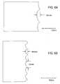
- FIGs. 6A and 6Bare representations of images from a scanning electron microscope that respectively show the etching results of the prior art process and the inventive process.
- the present inventionis a method and apparatus for etching a deep trench that comprises a plurality of cycles of plasma processing that are performed in situ within an etch reactor. Each such cycle comprises an etch step and a deposition step.
- the etch and deposition stepsare individual plasma processes that are defined by a composition of a gaseous mixture that is supplied into a reaction chamber of the etch reactor.
- the etch reactorgenerally is a reactor comprising a source of power for generating and maintaining a plasma (referred to herein as source power) and a source of power for biasing a substrate (referred to herein as bias power).
- the inventionuses pulsed bias power during the etch step to reduce scalloping of the trench sidewalls.
- the terms wafer and substrateare used interchangeably herein.
- the bias poweris deliberately pulsed while the source power is continuously applied.
- the methodetches trenches that have a width of about 1 to 20 ⁇ m and an aspect ratio of about 5 to 50. Such trenches are referred herein as deep trenches. Further examination of the process has revealed that the pulsing of the bias power reduces in-process charging of a surface of the trench, substantially reduces scalloping, increases the etch rate, and reduces notching of the sidewalls at a bottom of the trench.
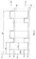
- FIGS. 1A-1Fdepict a sequence of schematic, cross-sectional views of a substrate that has an illustrative deep trench being formed in accordance with the present invention.
- the cross-sectional views in FIGS. 1A-1 Frelate to the individual processes that are used to form the trench.
- sub-processes and lithographic routinesi.e., exposure and development of photoresist and the like
- the images in FIGS. 1A-1Fare not depicted to scale and are simplified for illustrative purposes.
- FIG. 1Adepicts one illustrative example of a wafer 100 (e.g., a silicon wafer) having an etch stop layer 108, a layer 112 of material to etched, and an etch mask layer 102.
- the etch stop layer 108may be formed from silicon dioxide (SiO 2 ), silicon carbide (SiC), and the like.
- a material of the etch stop layer 108is selected to best define an end point during a deep trench etch process (discussed in reference to FIG. 1C below).
- the layer 112is generally a silicon layer that is deposited on the wafer 100 using a vacuum deposition method such as physical vapor deposition (PVD), chemical vapor deposition, and the like to a thickness of between 1 and 100 ⁇ m.
- PVDphysical vapor deposition
- chemical vapor depositionand the like to a thickness of between 1 and 100 ⁇ m.
- the layer 112may be formed from a material other than Si.
- the etch mask layer 102generally is a photoresist layer that is formed using a conventional photoresist application routine to a thickness of about 1 ⁇ m. Further, the mask layer 102 may comprise an anti-reflective layer (not shown) that controls a reflection of the light during exposure of the photoresist.
- the anti-reflective layergenerally is formed on the silicon layer 112 prior to application of the photoresist layer 102 or, alternatively, is deposited on top of the layer 102. As feature sizes are reduced, inaccuracies in an etch mask pattern transfer process can arise from optical limitations inherent to the lithographic process such as the light reflection.
- Such anti-reflective layermay be composed from silicon nitride (SiN), polyamides, and the like. In some applications, the anti-reflective layer may not be necessary. As such, the anti-reflective layer is considered optional.
- FIG. 1Bdepicts the wafer 100 after the photoresist layer 102 has been processed using a lithographic patterning routine, i.e., the photoresist is exposed through a patterned mask, developed, and then the undeveloped portion of the photoresist is removed.
- the remaining developed photoresistis generally a carbon-based polymer that forms an etch mask 104 on top of the wafer 100.
- the etch mask 104exposes a region 106 to further processing. As such, the etch mask 104 defines location and topographic dimensions of a trench to be formed in the layer 112.
- the layer 102may be formed from an inorganic material such silicon dioxide (SiO 2 ) to form a hard (inorganic) etch mask.
- an inorganic materialsuch as silicon dioxide (SiO 2 ) to form a hard (inorganic) etch mask.
- photoresistis applied over a layer of the inorganic material and the photoresist etch mask 104 is formed upon, as described above.
- the inorganic materialis removed in the region 106 using a dry or wet etch process followed by a photoresist stripping process. The stripping process leaves the hard etch mask resting upon the layer 112. Similar to the photoresist etch mask 104, the hard etch mask exposes the region 106 during etching the trench.
- FIGS. 1C and 1Ddepict a trench 110 being formed using a deep trench etch process that comprises a plurality of consecutive cycles that are serially performed in situ in an etch reactor. Each cycle comprises an etch step and a deposition step wherein, during the etch step, a source of the bias power is pulsed, while the plasma source power is continuously applied. Alternation of the etch and deposition steps is accomplished by replacing the gaseous mixture in the reaction chamber of the etch reactor and may be performed without termination of a plasma.
- FIG. 1Cdepicts the trench 110 after a deposition step of an intermediate cycle of the deep trench etch process.
- a passivation gasis excited to a plasma using a source power and little or no bias power applied to the substrate.
- the passivation gasforms a sacrificial film 118.
- the film 118is thin polymeric passivation layer that is deposited on the etch mask 104, sidewalls 114, and the bottom 116 of the trench 110 being etched.
- the deposition stepuses a passivation gas such as at least one of a fluorocarbon or hydrofluorocarbon gas, e.g., at least one of C 4 F 8 , CHF 3 , and the like to form the film 118.
- the passivation film 118 along the sidewalls of the trench 110has a thickness that, when the film is applied rapidly, decreases towards a bottom 116 of the trench 110.
- the thickness of the film 118may be controlled (e.g., by adjusting a duration of the deposition step) to leave the bottom 116 of the trench 110 uncoated by the film 118, and subsequently exposed to an etchant plasma (discussed in reference to FIG. 1 D below).
- the bottom 116may be thinly coated (as shown in FIG. 1 C), such that the etchant quickly removes the film at the bottom of the trench before further etching the trench deeper.
- FIG. 1Ddepicts the trench 100 after an etch step of an intermediate cycle of the deep trench etch process.
- the etch stepuses a high density plasma that comprises an etchant, such as sulfur hexafluoride (SF 6 ) and the like, to increase the etch rate and productivity.
- a source of the bias poweris pulsed while the plasma source power is continuously applied, as discussed above.
- the wafer bias poweris applied during the etch step for a duration between 1 and 30 msec at a duty cycle of between 10 and 90%.
- the SF 6 etchanthas a selectivity to silicon (layer 112) over photoresist (mask 104) or the polymeric passivation film 118 of about 100:1, and as such, facilitates etching of the deep trenches. Since the etchant consumes the etch mask 104 as the etch process proceeds, the sacrificial passivation film 118 is repeatedly deposited upon the mask after each etch step, in essence, to partially restore the etch mask 104. Note that in FIG. 1 D, after the etch step, the passivation film 118 is illustratively shown as resting only on the sidewalls 114. The film 118 protects the sidewalls 114 as well as improves anisotropy of the deep trench etch process, thus allowing fabrication of the trenches having a high aspect ratio, e.g., about 5 to 50.
- the inventive methodcan be performed, for example, in a Decoupled Plasma Source - Deep Trench (DPS-DT) reactor, which is a component of the CENTURA ® semiconductor wafer processing systems available from Applied Materials, Inc. of Santa Clara, California.
- DPS-DT reactoris discussed in detail with respect to FIG. 5 below.
- the DPS-DT reactoruses a 12.56 MHz inductive plasma source (source 518 in FIG. 4 below) to produce a high density plasma, while a wafer is biased by a 400kHz power source (source 522 in FIG. 5 below) of bias power that provides either a pulsed or continuous output.
- the DPS-DT reactorallows an independent control of ion energy and plasma density, has a wide process window over changes in the plasma source and bias power, pressure, and gas chemistries, and may use an endpoint detection system to determine an end of the etch process.
- the etch stepprovides SF 6 at a rate of 20 to 500 sccm, applies 200 to 3000 W of a plasma power and 0 to 300 W of a pulsed biasing power.
- the pulseshave a duration of between 1 and 30 msec at a duty cycle of between 10 and 90%.
- the reactormaintains a wafer temperature at 10 to 100 degrees Celsius and a pressure in the reaction chamber at 5 to 500 mTorr.
- One specific process recipeprovides SF 6 at a rate of 250 sccm , 1000 W from a plasma power source and 20 W from a pulsed biasing power source for 6 msec at a duty cycle of 33%, a wafer temperature of 10 degrees Celsius, and a chamber pressure of 20 mTorr.
- the deposition stepprovides C 4 F 8 at a rate of 20 to 500 sccm, applies 200 to 3000 W of a plasma power and 0 to 100 W of a biasing power, and maintains a wafer temperature at 10 to 100 degrees Celsius and a pressure in the reaction chamber at 10 to 100 mTorr.
- One specific process recipeprovides C 4 F 8 at a rate of 300 sccm, 1800 W from a plasma power source and no biasing power, a wafer temperature of 10 degrees Celsius, and a chamber pressure of 40 mTorr.
- the methodforms a trench, e.g., in silicon, having a width of about 1 to 20 ⁇ m and an aspect ratio of about 5 to 50. Further, the roughness of the sidewalls (i.e., scalloping pattern) is reduces to less than 0.1 ⁇ m. Those skilled in the art will appreciate that such dimensions should not be considered as limiting.
- FIG. 1Edepicts the wafer 100 after a deep trench 110 has been formed using the method of the present invention.
- the photoresist etch mask 104is depicted as partially consumed by the etchant plasma upon the completion of the etch step, as discussed above in reference to FIG. 1 D.
- the total duration of the deep trench etch processmay be controlled upon occurrence of a certain optical emission, e.g., by using an end point detector, upon a particular duration occurring, or some other indicator determining that the trench 110 has been etched to a desired depth.
- FIG. 1Fdepicts the wafer 100 comprising the deep trench 110 after the etch mask 104 has been removed using a conventional photoresist stripping process.
- the stripping processmay be performed, for example, in the Advanced Strip and Passivation (ASP) reactor of the CENTURA® system.
- the ASP reactoris a microwave downstream oxygen plasma reactor in which the plasma is confined to a plasma tube and only reactive neutrals are allowed to enter a process chamber. Such a plasma confinement scheme precludes plasma-related damage of the substrate or circuits formed on the substrate.
- the ASP reactorprovides temperature control of the wafer.
- the wafer back sidemay be heated (e.g., radiantly, by quartz halogen lamps) or cooled (e.g., providing an inert gas such as helium to backside of the wafer) to maintain a wafer temperature between 20 to 400 degrees Celsius.
- a duration of a stripping processgenerally is between 30 and 120 seconds.
- the photoresist etch mask 104may be stripped in the DPS-DT reactor.
- the stripping processprovides to the DPS-DT reactor oxygen (O 2 ) at a rate of 10 to 300 sccm as well as nitrogen (N 2 ) at a rate of 0 to 300 sccm (a flow ratio of O 2 : N 2 ranging from all oxygen to 1:30), applies 200 to 3000 W of a plasma power and 0 to 100 W of a biasing power, and maintains a wafer temperature at 10 to 100 degrees Celsius and a pressure in the reaction chamber at 5 to 500 mTorr.
- O 2oxygen
- N 2nitrogen
- One specific process recipeprovides O 2 at a rate of 100 sccm and N 2 at a rate of 0 sccm, 1000 W from a plasma power source and 0 W from a biasing power source, a wafer temperature of 10 degrees Celsius, and a chamber pressure of 30 mTorr.
- FIGS. 2 and 3are exemplary timing diagrams of a deep trench etch process that may be used to etch the deep trench 110 in the semiconductor wafer 100, as described above in reference to FIG. 1C.
- FIG. 2depicts a sequence of cycles 240 wherein each cycle 240 comprises a period 202 within which an etch process is performed and a period 222 within which a deposition process is performed. Together, a plurality of cycles 240 comprises a deep trench etch process 242.
- a first graph 200depicts a status (y-axis 210) of the etch process, where the etch process is in ON (204) and OFF (206) states versus time (x-axis 208).
- a second graph 220depicts a status (y-axis 230) of the deposition process, where the deposition process is in ON (224) and OFF (226) states versus time (x-axis 228).
- the deposition processis inactive (226).
- the deposition processis active (224).
- the etch period 202has a duration between 1 and 40 seconds, while the deposition period 222 has a duration between 1 and 20 seconds.
- the etch process duration 242begins with the deposition period 222 and ends with the etch period 202.
- the process 242may begin with the etch period 202 and end with the deposition period 222 and/or comprise one or more additional etch periods 202 at any time during execution of the etch duration 242.
- the etch duration 242generally comprises between 10 and 100 cycles 240 and has a duration between 1 and 40 seconds to etch a trench in silicon having a depth in a range between 1 and 20 ⁇ m.
- the duration of the individual periods 202 and 222may vary during the etch process due to various factors such as layer composition, layer thickness, and trench dimensions, and the like.
- FIG. 3depicts in detail one individual etch period 202 having an ON state.
- period 202comprises a sequence of time intervals 322 when a bias power is ON, and time intervals 336 when the bias power is OFF.
- a first graph 300depicts a status (y-axis 210) of an individual etch period 202
- a second graph 320depicts a status (y-axis 330) of the bias power.
- the graph 300depicts the ON (204) and OFF (206) states of the etch process versus time (x-axis 208).
- the second graph 320depicts the ON (324) and OFF (326) states of the bias power versus time (x-axis 328).
- the bias poweris applied during the time intervals 322 and is terminated during the time interval 336.
- each active time interval 202 of the etch processis associated with a plurality of bias power pulses, represented the time intervals 322 and 336.
- a deep trench having a width of about 1 to 20 ⁇ m and an aspect ratio of about 5 to 50may be formed in a silicon wafer by providing the etch step 202 for about 10 seconds and the deposition step 222 for about 5 seconds.
- the etch stepapplies a pulse 332 of the bias power during the time intervals 322 having a duration of about 6 msec and terminates the bias power during the time intervals 336 having a duration of about 12 msec (i.e., maintaining a 33% duty cycle).
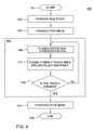
- FIG 4is a flow diagram of a method 400 for plasma etching a deep trench in accordance with the present invention.
- the method 400may be used to form the trenches upon a semiconductor substrate, such as those used to fabricate Micro Electro-Mechanic Systems (MEMS).
- MEMSMicro Electro-Mechanic Systems
- the method 400begins at step 401 and proceeds to step 402.
- a film stackis formed upon a substrate such as the silicon wafer 100, as described above with regard to FIG. 1A.
- the film stackcomprises an etch stop layer (e.g., silicon nitride layer 108) and, for example, the silicon layer 112.
- a photoresist etch maske.g., the etch mask 104 is formed on the silicon layer 112 to define the trench 110 to be etched, as described above with regard to FIG. 1 B.
- the deep trench etch processis performed.
- Such etch processcomprises a period 408 of depositing a protective polymeric film upon the etch mask and sidewalls of trench being etched, a period 410 of etching the trench in the silicon layer, and a decision step 412.
- step 406uses a plasma comprising a polymer-producing fluorocarbon or hydrofluorocarbon gas (e.g., C 4 F 8 ), as described above with regard to FIG. 1 C.
- a plasmacomprising a polymer-producing fluorocarbon or hydrofluorocarbon gas (e.g., C 4 F 8 ), as described above with regard to FIG. 1 C.
- the period 408continues during the time interval 222, as shown in FIG. 2.
- step 408uses a plasma comprising sulfur hexafluoride, as described above with regard to FIG. 1 D.
- the period 410continues during the time interval 202, as shown in FIG. 2.
- a source of the bias power for biasing a wafer support pedestal 516(discussed in reference to FIG. 5 below) is pulsed.
- the bias poweris applied during the period 410 for a duration between 1 and 30 msec at a duty cycle of between 10 and 90%.
- the method 400queries whether the trench has been formed (e.g., etched to a predetermined depth, such as defined by the etch stop layer).
- the decision making routinemay be automated using an end-point detection technique. For example, when the etch stop layer is formed from silicon nitride, the endpoint detection system of the referred to DPS-DT reactor may monitor plasma emissions, e.g., at a wavelength of about 288 nm, to determine if the trench has been formed, as described above with regard to FIG. 1 E.
- the method 400repeats step 406 until the trench 110 is formed.
- the deep trench etch processcomprises a plurality of consecutive cycles of depositing a protective polymeric film 118 and etching the silicon layer 112. If the query of step 412 is affirmatively answered, the method 400 proceeds to step 414.
- the etch maskis stripped from the silicon layer 112 using, e.g., a plasma stripping process, as described above with regard to FIG. 1 F.
- the method 400ends.
- FIGs. 6A and 6Bare representations of images from a scanning electron microscope (SEM) that show the sidewall of a trench formed with the foregoing process comprising substantially less scalloping at the sidewalls than results from using a prior art process.
- the resulting trench sidewallhas peak-to-valley scallops of less than 100 nm as compared to about 200 nm scallops (FIG. 6B) that result from prior art etch processes.
- the scallopingwas reduced by the inventive process to about 65 nm.
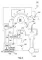
- FIG. 5depicts a schematic diagram of the DPS-DT reactor 500 that may be used to accomplish the method of the present invention.
- the reactor 500comprises a process chamber 510 having a wafer support pedestal 516 within a conductive body (wall) 530, and a controller 540.
- the support pedestal (cathode) 516is coupled, through a first matching network 524, to a biasing power source 522.
- the source 522generally is capable of producing up to 500 W of continuous and pulsed power at a tunable frequency in a range from 50 kHz to 13.56 MHz. In other embodiments, the source 522 may be a DC or pulsed DC source.
- the wall 530is supplied with a dome-shaped dielectric ceiling 520. Other modifications of the chamber 510 may have other types of ceilings, e.g., a flat ceiling. Typically, the wall 530 is coupled to an electrical ground 534. Above the ceiling 520 is disposed an inductive coil antenna 512.
- the antenna 512is coupled, through a second matching network 519, to a plasma power source 518.
- the source 518typically is capable of producing up to 3000 W at a tunable frequency in a range from 50 kHz to 13.56 MHz.
- a controller 540comprises a central processing unit (CPU) 544, a memory 542, and support circuits 546 for the CPU 544 and facilitates control of the components of the DPS etch process chamber 510 and, as such, of the etch process, as discussed below in further detail.
- CPUcentral processing unit
- a semiconductor wafer 514is placed on the pedestal 516 and process gases are supplied from a gas panel 538 through entry ports 526 and form a gaseous mixture 550.
- the gaseous mixture 550is ignited into a plasma 555 in the chamber 510 by applying power from the sources 518 and 522 to the antenna 512 and the cathode 516, respectively.
- the pressure within the interior of the chamber 510is controlled using a throttle valve 527 and a vacuum pump 536.
- the temperature of the chamber wall 530is controlled using liquid-containing conduits (not shown) that run through the wall 530.
- the temperature of the wafer 514is controlled by stabilizing a temperature of the support pedestal 516.
- the helium gas from a source 548is provided via a gas conduit 549 to channels formed by the back of the wafer 514 and grooves (not shown) on the pedestal surface.
- the helium gasis used to facilitate heat transfer between the pedestal 516 and the wafer 514.
- the pedestal 516may be heated by a resistive heater (not shown) within the pedestal to a steady state temperature and then the helium gas facilitates uniform heating of the wafer 514.
- the wafer 514is maintained at a temperature of between 10 and 500 degrees Celsius.
- etch chambersmay be used to practice the invention, including chambers with remote plasma sources, microwave plasma chambers, electron cyclotron resonance (ECR) plasma chambers, and the like.
- ECRelectron cyclotron resonance
- the controller 540may be one of any form of general purpose computer processor that can be used in an industrial setting for controlling various chambers and sub-processors.
- the memory 542is coupled to the CPU 544.
- the memory 542, or computer-readable mediummay be one or more of readily available memory such as random access memory (RAM), read only memory (ROM), floppy disk, hard disk, or any other form of digital storage, local or remote.
- the support circuits 546are coupled to the CPU 544 for supporting the processor in a conventional manner. These circuits include cache, power supplies, clock circuits, input/output circuitry and subsystems, and the like.
- Software routines that, when executed by the CPU 544, cause the reactor to perform processes of the present inventionare generally stored in the memory 542.
- the software routinesmay also be stored and/or executed by a second CPU (not shown) that is remotely located from the hardware being controlled by the CPU 544.
- the software routinesare executed after the wafer 514 is positioned on the pedestal 516.
- the software routineswhen executed by the CPU 544, transform the general purpose computer into a specific purpose computer (controller) 540 that controls the chamber operation such that the etching process is performed in accordance with the method of the present invention.
- the present inventionis discussed as being implemented as a software routine, some of the method steps that are disclosed herein may be performed in hardware as well as by the software controller. As such, the invention may be implemented in software as executed upon a computer system, in hardware as an application specific integrated circuit (ASIC), or other type of hardware implementation, or a combination of software and hardware.
- ASICapplication specific integrated circuit
Landscapes
- Engineering & Computer Science (AREA)
- Physics & Mathematics (AREA)
- Manufacturing & Machinery (AREA)
- Microelectronics & Electronic Packaging (AREA)
- Plasma & Fusion (AREA)
- Condensed Matter Physics & Semiconductors (AREA)
- General Physics & Mathematics (AREA)
- Computer Hardware Design (AREA)
- Power Engineering (AREA)
- Geometry (AREA)
- Drying Of Semiconductors (AREA)
Abstract
Description
The present invention generally relates to semiconductor substrateprocessing systems. More specifically, the present invention relates to a method andapparatus for performing an etch process in a semiconductor substrate processingsystem.
Micro Electro-Mechanic Systems, or MEMS, are very small electro-mechanicaldevices such as actuators, sensors, and the like. Unlike conventionalmechanical devices, MEMS are generally fabricated on a semiconductor substratesuch as a silicon (Si) wafer and may be monolithically integrated with electronic circuitsthat are formed on the same substrate.
Manufacturing of MEMS comprises processes that have limited analogies tothe fabrication of electronic integrated circuits on semiconductor substrates. One suchprocess is a process of etching a trench having a width of about 1 to 20 µm and anaspect ratio of about 5 to 50 or more. Herein such trenches are referred as deeptrenches and the term aspect ratio refers to a height of the trench divided by its width.
A deep trench is generally formed using an etch process, e.g., a TimeMultiplex Gas Modulation (TMGM) process, which comprises a plurality of alternatingcycles of etching and deposition that are serially performed in a single etch reactor, i.e.,in situ. More specifically, the TMGM etch process is a plasma process that forms ahigh aspect ratio trench at a high etch rate. The TMGM process etches a material for aperiod of time then deposits a protective film upon the previously etched surface toprotect the surface, typically the sidewalls of the trench, from further etching. Thesetwo steps are repeated as a deeper and deeper trench is formed.
As a result of the TMGM etch process, the sidewall of the trench acquires aperiodic pattern of variations in the width with the depth of the trench, i.e., a scalloping pattern forms along the depth of the trench. The scalloping pattern is originated by analternating nature of cycles of etching and deposition and may comprise "peaks" and"valleys" having a lateral height of about 0.2-0.4 µm. Such patterning of the sidewall isa drawback of the TMGM etch process. The scalloping pattern increases roughness ofa sidewall surface of the trench and may render an electro-mechanical device such asMEMS to operate sub-optimally or not at all.
Therefore, there is a need in the art for a method and apparatus for etching adeep trench in a semiconductor substrate during fabrication of MEMS or othersemiconductor devices such that the trench has reduced scalloping.
This problem is solved by the method according to claim 1 and the computer-readablemedium according to claim 14, the latter being a computer-related invention.
Preferred embodiments, aspects and improvements of the invention are disclosed in thedescription, the figures and the depending claims.
The invention is a computer-related invention, which is also directed to an apparatus forcarrying out the disclosed method. These steps may be performed by way of hardwarecomponents, a computer programmed by appropriate software, by any combination of the twoor in any other manner. Furthermore, the invention is also directed to methods by which thedescribed apparatus operates.
A method for plasma etching a trench in a semiconductor substrate using aplurality of processing cycles comprising plasma etch and deposition periods, whereina substrate bias power is pulsed during the etch periods. In one embodiment foretching a deep trench in a silicon substrate, the deposition period is performed using afluorocarbon or hydrofluorocarbon that forms a protective polymeric coating on thesidewalls of the trench, and the etch period is performed using sulfur hexafluoride. Asa result of the pulsed bias power, the resulting trench has side walls that aresubstantially less scalloped than the scalloping of the prior art.
The teachings of the present invention can be readily understood byconsidering the following detailed description in conjunction with the accompanyingdrawings, in which:
FIGS. 1A-1F together depict a sequence of schematic, cross-sectional viewsof a substrate illustratively having a deep trench being formed in accordance with thepresent invention;
FIG. 2 is a timing diagram of an etch process in accordance with oneembodiment of the present invention;
FIG. 3 is a timing diagram of a substrate bias power during an etch step of aprocess of FIG. 1 in accordance with one embodiment of the present invention;
FIG. 4 depicts a flow diagram of a method for plasma etching a deep trenchin accordance with the present invention;
FIG. 5 depicts a schematic diagram of a plasma processing apparatus of thekind used in performing the etch process according to one embodiment of the presentinvention; and
FIGs. 6A and 6B are representations of images from a scanning electronmicroscope that respectively show the etching results of the prior art process and theinventive process.
To facilitate understanding, identical reference numerals have been used,where possible, to designate identical elements that are common to the figures.
It is to be noted, however, that the appended drawings illustrate only typicalembodiments of this invention, and are therefore not to be considered limiting of itsscope, for the invention may admit to other equally effective embodiments.
The present invention is a method and apparatus for etching a deep trenchthat comprises a plurality of cycles of plasma processing that are performed in situwithin an etch reactor. Each such cycle comprises an etch step and a deposition step.The etch and deposition steps are individual plasma processes that are defined by acomposition of a gaseous mixture that is supplied into a reaction chamber of the etchreactor. The etch reactor generally is a reactor comprising a source of power forgenerating and maintaining a plasma (referred to herein as source power) and asource of power for biasing a substrate (referred to herein as bias power). Theinvention uses pulsed bias power during the etch step to reduce scalloping of thetrench sidewalls. The terms wafer and substrate are used interchangeably herein.
In the inventive method, during the etch step, the bias power is deliberatelypulsed while the source power is continuously applied. In one embodiment, the methodetches trenches that have a width of about 1 to 20 µm and an aspect ratio of about 5 to50. Such trenches are referred herein as deep trenches. Further examination of theprocess has revealed that the pulsing of the bias power reduces in-process charging ofa surface of the trench, substantially reduces scalloping, increases the etch rate, andreduces notching of the sidewalls at a bottom of the trench.
FIGS. 1A-1F depict a sequence of schematic, cross-sectional views of asubstrate that has an illustrative deep trench being formed in accordance with thepresent invention. The cross-sectional views in FIGS. 1A-1 F relate to the individualprocesses that are used to form the trench. For purposes of clarity, sub-processes andlithographic routines (i.e., exposure and development of photoresist and the like)known in the art are not shown in FIGS. 1A-1F. The images in FIGS. 1A-1F are notdepicted to scale and are simplified for illustrative purposes.
FIG. 1A depicts one illustrative example of a wafer 100 (e.g., a silicon wafer)having anetch stop layer 108, alayer 112 of material to etched, and anetch masklayer 102. Theetch stop layer 108 may be formed from silicon dioxide (SiO2), siliconcarbide (SiC), and the like. A material of theetch stop layer 108 is selected to bestdefine an end point during a deep trench etch process (discussed in reference to FIG.1C below). Thelayer 112 is generally a silicon layer that is deposited on thewafer 100using a vacuum deposition method such as physical vapor deposition (PVD), chemicalvapor deposition, and the like to a thickness of between 1 and 100 µm. However, thelayer 112 may be formed from a material other than Si.
Theetch mask layer 102 generally is a photoresist layer that is formed usinga conventional photoresist application routine to a thickness of about 1 µm. Further,themask layer 102 may comprise an anti-reflective layer (not shown) that controls areflection of the light during exposure of the photoresist. The anti-reflective layergenerally is formed on thesilicon layer 112 prior to application of thephotoresist layer 102 or, alternatively, is deposited on top of thelayer 102. As feature sizes are reduced,inaccuracies in an etch mask pattern transfer process can arise from optical limitations inherent to the lithographic process such as the light reflection. Such anti-reflectivelayer may be composed from silicon nitride (SiN), polyamides, and the like. In someapplications, the anti-reflective layer may not be necessary. As such, the anti-reflectivelayer is considered optional.
FIG. 1B depicts thewafer 100 after thephotoresist layer 102 has beenprocessed using a lithographic patterning routine, i.e., the photoresist is exposedthrough a patterned mask, developed, and then the undeveloped portion of thephotoresist is removed. The remaining developed photoresist is generally a carbon-basedpolymer that forms anetch mask 104 on top of thewafer 100. Theetch mask 104 exposes aregion 106 to further processing. As such, theetch mask 104 defineslocation and topographic dimensions of a trench to be formed in thelayer 112.
In an alternative embodiment (not shown), thelayer 102 may be formed froman inorganic material such silicon dioxide (SiO2) to form a hard (inorganic) etch mask.In this embodiment, photoresist is applied over a layer of the inorganic material and thephotoresist etch mask 104 is formed upon, as described above. Further, the inorganicmaterial is removed in theregion 106 using a dry or wet etch process followed by aphotoresist stripping process. The stripping process leaves the hard etch mask restingupon thelayer 112. Similar to thephotoresist etch mask 104, the hard etch maskexposes theregion 106 during etching the trench.
FIGS. 1C and 1D depict atrench 110 being formed using a deep trench etchprocess that comprises a plurality of consecutive cycles that are serially performed insitu in an etch reactor. Each cycle comprises an etch step and a deposition stepwherein, during the etch step, a source of the bias power is pulsed, while the plasmasource power is continuously applied. Alternation of the etch and deposition steps isaccomplished by replacing the gaseous mixture in the reaction chamber of the etchreactor and may be performed without termination of a plasma.
FIG. 1C depicts thetrench 110 after a deposition step of an intermediatecycle of the deep trench etch process. During the deposition step, a passivation gas isexcited to a plasma using a source power and little or no bias power applied to thesubstrate. As such, the passivation gas forms asacrificial film 118. Specifically, thefilm 118 is thin polymeric passivation layer that is deposited on theetch mask 104,sidewalls 114, and thebottom 116 of thetrench 110 being etched. The deposition stepuses a passivation gas such as at least one of a fluorocarbon or hydrofluorocarbongas, e.g., at least one of C4F8, CHF3, and the like to form thefilm 118. Thepassivationfilm 118 along the sidewalls of thetrench 110 has a thickness that, when the film isapplied rapidly, decreases towards abottom 116 of thetrench 110. The thickness ofthefilm 118 may be controlled (e.g., by adjusting a duration of the deposition step) toleave thebottom 116 of thetrench 110 uncoated by thefilm 118, and subsequentlyexposed to an etchant plasma (discussed in reference to FIG. 1 D below). In a secondembodiment, the bottom 116 may be thinly coated (as shown in FIG. 1 C), such that theetchant quickly removes the film at the bottom of the trench before further etching thetrench deeper.
FIG. 1D depicts thetrench 100 after an etch step of an intermediate cycle ofthe deep trench etch process. The etch step uses a high density plasma thatcomprises an etchant, such as sulfur hexafluoride (SF6) and the like, to increase theetch rate and productivity. In the present invention, during the etch step, a source ofthe bias power is pulsed while the plasma source power is continuously applied, asdiscussed above. In one embodiment, the wafer bias power is applied during the etchstep for a duration between 1 and 30 msec at a duty cycle of between 10 and 90%.The SF6 etchant has a selectivity to silicon (layer 112) over photoresist (mask 104) orthepolymeric passivation film 118 of about 100:1, and as such, facilitates etching ofthe deep trenches. Since the etchant consumes theetch mask 104 as the etchprocess proceeds, thesacrificial passivation film 118 is repeatedly deposited upon themask after each etch step, in essence, to partially restore theetch mask 104. Note thatin FIG. 1 D, after the etch step, thepassivation film 118 is illustratively shown as restingonly on thesidewalls 114. Thefilm 118 protects thesidewalls 114 as well as improvesanisotropy of the deep trench etch process, thus allowing fabrication of the trencheshaving a high aspect ratio, e.g., about 5 to 50.
The inventive method can be performed, for example, in a DecoupledPlasma Source - Deep Trench (DPS-DT) reactor, which is a component of theCENTURA ® semiconductor wafer processing systems available from AppliedMaterials, Inc. of Santa Clara, California. The DPS-DT reactor is discussed in detail with respect to FIG. 5 below. In one embodiment, the DPS-DT reactor uses a 12.56MHz inductive plasma source (source 518 in FIG. 4 below) to produce a high densityplasma, while a wafer is biased by a 400kHz power source (source 522 in FIG. 5below) of bias power that provides either a pulsed or continuous output. The DPS-DTreactor allows an independent control of ion energy and plasma density, has a wideprocess window over changes in the plasma source and bias power, pressure, and gaschemistries, and may use an endpoint detection system to determine an end of theetch process.
In an exemplary embodiment, where a DPS-DT reactor is used to etchtrenches 110 in silicon, the etch step provides SF6 at a rate of 20 to 500 sccm, applies200 to 3000 W of a plasma power and 0 to 300 W of a pulsed biasing power. Thepulses have a duration of between 1 and 30 msec at a duty cycle of between 10 and90%. The reactor maintains a wafer temperature at 10 to 100 degrees Celsius and apressure in the reaction chamber at 5 to 500 mTorr. One specific process recipeprovides SF6 at a rate of 250 sccm , 1000 W from a plasma power source and 20 Wfrom a pulsed biasing power source for 6 msec at a duty cycle of 33%, a wafertemperature of 10 degrees Celsius, and a chamber pressure of 20 mTorr.
In this illustrative embodiment, the deposition step provides C4F8 at a rate of20 to 500 sccm, applies 200 to 3000 W of a plasma power and 0 to 100 W of abiasing power, and maintains a wafer temperature at 10 to 100 degrees Celsius and apressure in the reaction chamber at 10 to 100 mTorr. One specific process recipeprovides C4F8 at a rate of 300 sccm, 1800 W from a plasma power source and nobiasing power, a wafer temperature of 10 degrees Celsius, and a chamber pressure of40 mTorr.
In one embodiment, the method forms a trench, e.g., in silicon, having awidth of about 1 to 20 µm and an aspect ratio of about 5 to 50. Further, the roughnessof the sidewalls (i.e., scalloping pattern) is reduces to less than 0.1 µm. Those skilled inthe art will appreciate that such dimensions should not be considered as limiting.
FIG. 1E depicts thewafer 100 after adeep trench 110 has been formedusing the method of the present invention. In FIG. 1E, thephotoresist etch mask 104 is depicted as partially consumed by the etchant plasma upon the completion of the etchstep, as discussed above in reference to FIG. 1 D. The total duration of the deep trenchetch process may be controlled upon occurrence of a certain optical emission, e.g., byusing an end point detector, upon a particular duration occurring, or some otherindicator determining that thetrench 110 has been etched to a desired depth.
FIG. 1F depicts thewafer 100 comprising thedeep trench 110 after theetchmask 104 has been removed using a conventional photoresist stripping process. Thestripping process may be performed, for example, in the Advanced Strip andPassivation (ASP) reactor of the CENTURA® system. The ASP reactor is a microwavedownstream oxygen plasma reactor in which the plasma is confined to a plasma tubeand only reactive neutrals are allowed to enter a process chamber. Such a plasmaconfinement scheme precludes plasma-related damage of the substrate or circuitsformed on the substrate. The ASP reactor provides temperature control of the wafer.The wafer back side may be heated (e.g., radiantly, by quartz halogen lamps) orcooled (e.g., providing an inert gas such as helium to backside of the wafer) tomaintain a wafer temperature between 20 to 400 degrees Celsius. A duration of astripping process generally is between 30 and 120 seconds.
Alternatively, thephotoresist etch mask 104 may be stripped in the DPS-DTreactor. In one embodiment, the stripping process provides to the DPS-DT reactoroxygen (O2) at a rate of 10 to 300 sccm as well as nitrogen (N2) at a rate of 0 to 300sccm (a flow ratio of O2: N2 ranging from all oxygen to 1:30), applies 200 to 3000 W ofa plasma power and 0 to 100 W of a biasing power, and maintains a wafertemperature at 10 to 100 degrees Celsius and a pressure in the reaction chamber at 5to 500 mTorr. One specific process recipe provides O2 at a rate of 100 sccm and N2 ata rate of 0 sccm, 1000 W from a plasma power source and 0 W from a biasing powersource, a wafer temperature of 10 degrees Celsius, and a chamber pressure of 30mTorr.
FIGS. 2 and 3 are exemplary timing diagrams of a deep trench etch processthat may be used to etch thedeep trench 110 in thesemiconductor wafer 100, asdescribed above in reference to FIG. 1C.
FIG. 2 depicts a sequence ofcycles 240 wherein eachcycle 240 comprises aperiod 202 within which an etch process is performed and aperiod 222 within whicha deposition process is performed. Together, a plurality ofcycles 240 comprises adeeptrench etch process 242. Afirst graph 200 depicts a status (y-axis 210) of theetch process, where the etch process is in ON (204) and OFF (206) states versus time(x-axis 208). Correspondingly, a second graph 220 (below) depicts a status (y-axis230) of the deposition process, where the deposition process is in ON (224) and OFF(226) states versus time (x-axis 228). Specifically, during thetime interval 202 of thecycle 240 where the etch process is active (204), the deposition process is inactive(226). Similarly, during thetime interval 222 of thecycle 240 where the etch process isinactive (206), the deposition process is active (224). One skilled in the art willunderstand that the time required to switch between the etching and depositionprocesses in eachcycle 240 is not shown.
In one embodiment where thetrench 110 is etched in a silicon wafer, theetch period 202 has a duration between 1 and 40 seconds, while thedeposition period 222 has a duration between 1 and 20 seconds. In FIG. 2, theetch process duration 242 begins with thedeposition period 222 and ends with theetch period 202.Alternatively, theprocess 242 may begin with theetch period 202 and end with thedeposition period 222 and/or comprise one or moreadditional etch periods 202 at anytime during execution of theetch duration 242. Theetch duration 242 generallycomprises between 10 and 100cycles 240 and has a duration between 1 and 40seconds to etch a trench in silicon having a depth in a range between 1 and 20µm.One skilled in the art will appreciate that the duration of theindividual periods
FIG. 3 depicts in detail oneindividual etch period 202 having an ON state. Inaccordance with the present invention,period 202 comprises a sequence oftimeintervals 322 when a bias power is ON, andtime intervals 336 when the bias power isOFF. Specifically, in FIG. 3, afirst graph 300 depicts a status (y-axis 210) of anindividual etch period 202, while a second graph 320 (below) depicts a status (y-axis330) of the bias power. Similar to thegraph 200 in FIG. 2, thegraph 300 depicts theON (204) and OFF (206) states of the etch process versus time (x-axis 208).Correspondingly, thesecond graph 320 depicts the ON (324) and OFF (326) states of the bias power versus time (x-axis 328). During theetch period 202, the bias power isapplied during thetime intervals 322 and is terminated during thetime interval 336. Assuch, eachactive time interval 202 of the etch process is associated with a plurality ofbias power pulses, represented thetime intervals
In one exemplary embodiment, a deep trench having a width of about 1 to 20µm and an aspect ratio of about 5 to 50 may be formed in a silicon wafer by providingtheetch step 202 for about 10 seconds and thedeposition step 222 for about 5seconds. The etch step applies apulse 332 of the bias power during thetime intervals 322 having a duration of about 6 msec and terminates the bias power during thetimeintervals 336 having a duration of about 12 msec (i.e., maintaining a 33% duty cycle).
Figure 4 is a flow diagram of amethod 400 for plasma etching a deep trenchin accordance with the present invention. Themethod 400 may be used to form thetrenches upon a semiconductor substrate, such as those used to fabricate MicroElectro-Mechanic Systems (MEMS).
Themethod 400 begins atstep 401 and proceeds to step 402. Atstep 402,a film stack is formed upon a substrate such as thesilicon wafer 100, as describedabove with regard to FIG. 1A. The film stack comprises an etch stop layer (e.g., siliconnitride layer 108) and, for example, thesilicon layer 112. Atstep 404, a photoresistetch mask (e.g., the etch mask 104) is formed on thesilicon layer 112 to define thetrench 110 to be etched, as described above with regard to FIG. 1 B.
Further, atstep 406, the deep trench etch process is performed. Such etchprocess comprises aperiod 408 of depositing a protective polymeric film upon the etchmask and sidewalls of trench being etched, aperiod 410 of etching the trench in thesilicon layer, and adecision step 412.
During theperiod 408, step 406 uses a plasma comprising a polymer-producingfluorocarbon or hydrofluorocarbon gas (e.g., C4F8), as described above withregard to FIG. 1 C. Theperiod 408 continues during thetime interval 222, as shown inFIG. 2.
During theperiod 410, step 408 uses a plasma comprising sulfurhexafluoride, as described above with regard to FIG. 1 D. Theperiod 410 continuesduring thetime interval 202, as shown in FIG. 2. In the present invention, duringperiod 410, a source of the bias power for biasing a wafer support pedestal 516 (discussed inreference to FIG. 5 below) is pulsed.
In one embodiment, the bias power is applied during theperiod 410 for aduration between 1 and 30 msec at a duty cycle of between 10 and 90%. Atstep 412,themethod 400 queries whether the trench has been formed (e.g., etched to apredetermined depth, such as defined by the etch stop layer). In a computerizedreactor (for example, in the DPS-DT reactor), atstep 412, the decision making routinemay be automated using an end-point detection technique. For example, when theetch stop layer is formed from silicon nitride, the endpoint detection system of thereferred to DPS-DT reactor may monitor plasma emissions, e.g., at a wavelength ofabout 288 nm, to determine if the trench has been formed, as described above withregard to FIG. 1 E.
If the query ofstep 412 is negatively answered, themethod 400 repeats step406 until thetrench 110 is formed. As such, the deep trench etch process comprises aplurality of consecutive cycles of depositing aprotective polymeric film 118 and etchingthesilicon layer 112. If the query ofstep 412 is affirmatively answered, themethod 400proceeds to step 414. Atstep 414, the etch mask is stripped from thesilicon layer 112using, e.g., a plasma stripping process, as described above with regard to FIG. 1 F. Atstep 416, themethod 400 ends.
FIGs. 6A and 6B are representations of images from a scanning electronmicroscope (SEM) that show the sidewall of a trench formed with the foregoingprocess comprising substantially less scalloping at the sidewalls than results fromusing a prior art process. For example, in one embodiment, the resulting trenchsidewall (FIG. 6A) has peak-to-valley scallops of less than 100 nm as compared toabout 200 nm scallops (FIG. 6B) that result from prior art etch processes. In onespecific embodiment of the invention, the scalloping was reduced by the inventiveprocess to about 65 nm.
FIG. 5 depicts a schematic diagram of the DPS-DT reactor 500 that may beused to accomplish the method of the present invention. Thereactor 500 comprises aprocess chamber 510 having awafer support pedestal 516 within a conductive body(wall) 530, and acontroller 540.
The support pedestal (cathode) 516 is coupled, through afirst matchingnetwork 524, to a biasingpower source 522. Thesource 522 generally is capable ofproducing up to 500 W of continuous and pulsed power at a tunable frequency in arange from 50 kHz to 13.56 MHz. In other embodiments, thesource 522 may be a DCor pulsed DC source. Thewall 530 is supplied with a dome-shapeddielectric ceiling 520. Other modifications of thechamber 510 may have other types of ceilings, e.g., aflat ceiling. Typically, thewall 530 is coupled to anelectrical ground 534. Above theceiling 520 is disposed aninductive coil antenna 512. Theantenna 512 is coupled,through asecond matching network 519, to aplasma power source 518. Thesource 518 typically is capable of producing up to 3000 W at a tunable frequency in a rangefrom 50 kHz to 13.56 MHz.
Acontroller 540 comprises a central processing unit (CPU) 544, a memory542, and supportcircuits 546 for theCPU 544 and facilitates control of the componentsof the DPSetch process chamber 510 and, as such, of the etch process, as discussedbelow in further detail.
In operation, asemiconductor wafer 514 is placed on thepedestal 516 andprocess gases are supplied from agas panel 538 throughentry ports 526 and form agaseous mixture 550. Thegaseous mixture 550 is ignited into aplasma 555 in thechamber 510 by applying power from thesources antenna 512 andthecathode 516, respectively. The pressure within the interior of thechamber 510 iscontrolled using athrottle valve 527 and avacuum pump 536. The temperature of thechamber wall 530 is controlled using liquid-containing conduits (not shown) that runthrough thewall 530.
The temperature of thewafer 514 is controlled by stabilizing a temperatureof thesupport pedestal 516. In one embodiment, the helium gas from asource 548 is provided via agas conduit 549 to channels formed by the back of thewafer 514 andgrooves (not shown) on the pedestal surface. The helium gas is used to facilitate heattransfer between thepedestal 516 and thewafer 514. During the processing, thepedestal 516 may be heated by a resistive heater (not shown) within the pedestal to asteady state temperature and then the helium gas facilitates uniform heating of thewafer 514. Using thermal control, thewafer 514 is maintained at a temperature ofbetween 10 and 500 degrees Celsius.
Those skilled in the art will understand that other forms of etch chambersmay be used to practice the invention, including chambers with remote plasmasources, microwave plasma chambers, electron cyclotron resonance (ECR) plasmachambers, and the like.
To facilitate control of the chamber as described above, thecontroller 540may be one of any form of general purpose computer processor that can be used in anindustrial setting for controlling various chambers and sub-processors. The memory542 is coupled to theCPU 544. The memory 542, or computer-readable medium, maybe one or more of readily available memory such as random access memory (RAM),read only memory (ROM), floppy disk, hard disk, or any other form of digital storage,local or remote. Thesupport circuits 546 are coupled to theCPU 544 for supporting theprocessor in a conventional manner. These circuits include cache, power supplies,clock circuits, input/output circuitry and subsystems, and the like. Software routinesthat, when executed by theCPU 544, cause the reactor to perform processes of thepresent invention are generally stored in the memory 542. The software routines mayalso be stored and/or executed by a second CPU (not shown) that is remotely locatedfrom the hardware being controlled by theCPU 544.
The software routines are executed after thewafer 514 is positioned on thepedestal 516. The software routines, when executed by theCPU 544, transform thegeneral purpose computer into a specific purpose computer (controller) 540 thatcontrols the chamber operation such that the etching process is performed inaccordance with the method of the present invention.
Although the present invention is discussed as being implemented as asoftware routine, some of the method steps that are disclosed herein may beperformed in hardware as well as by the software controller. As such, the inventionmay be implemented in software as executed upon a computer system, in hardware asan application specific integrated circuit (ASIC), or other type of hardwareimplementation, or a combination of software and hardware.
Although the forgoing discussion referred to fabrication of a deep trenchused in MEMS, fabrication of other structures and features used in the MEMS orintegrated electronic circuits can benefit from the invention. The invention can bepracticed in other etch semiconductor processing systems wherein the processingparameters may be adjusted to achieve acceptable characteristics by those skilled inthe art by utilizing the teachings disclosed herein without departing from the spirit of theinvention.
Claims (26)
- A method for plasma etching a trench in a semiconductor substrate to reducescalloping of the trench, comprising:applying a plurality of processing cycles to the substrate, where each cyclecomprises a plasma etch period and a plasma deposition period; andpulsing a substrate bias power during the plasma etch period.
- The method of claim 1 wherein the trench has a width between 1 to 20 µm andan aspect ratio of about 5 to 50.
- The method according to any one of the preceding claims wherein the trenchhas scallops having a peak-to-valley size that is less than 100 nm.
- The method according to any one of the preceding claims wherein the plasmaetch period has a duration between 1 and 40 seconds.
- The method according to any one of the preceding claims wherein the plasmaetch period comprises a plasma etch process that uses an etchant gas comprisingSF6.
- The method according to any one of the preceding claims wherein the plasmadeposition period has a duration between 1 and 20 seconds.
- The method according to any one of the preceding claims wherein the plasmadeposition period comprises a plasma process that uses at least one of afluorocarbon gas and a hydrofluorocarbon gas.
- The method of claim 7 wherein the fluorocarbon gas comprises C4F8.
- The method according to claim 7 or 8 wherein the hydrofluorocarbon gascomprises CHF3.
- The method according to any one of the preceding claims wherein the pulsingstep further comprises:applying the substrate bias power between 1 and 30 milliseconds at a dutycycle of between 10 and 90%.
- The method according to any one of the preceding claims wherein the pulsingstep further comprises:applying the substrate bias power for about 6 milliseconds at a duty cycle ofabout 33%.
- The method according to any one of the preceding claims wherein a sourcepower is continuously applied to the plasma while the substrate bias power is pulsed.
- The method of claim 12 wherein the source power has a frequency of about12.56 MHz and the substrate bias power has a frequency of about 400 KHz.
- A computer-readable medium including software that, when executed by aprocessor, performs a method that causes an etch reactor to etch a trench in asemiconductor substrate to reduce scalloping of the trench, comprising:applying a plurality of processing cycles to the substrate, where each cyclecomprises a plasma etch period and a plasma deposition period; andpulsing a substrate bias power during the plasma etch period.
- The computer-readable medium of claim 14 wherein the trench has a widthbetween 1 to 20 µm and an aspect ratio of about 5 to 50.
- The computer-readable medium according to claim 14 or 15 wherein thetrench has scallops having a peak-to-valley size that is less than 100 nm.
- The computer-readable medium according to any one of the claims 14 to 16wherein the plasma etch period has a duration between 1 and 40 seconds.
- The computer-readable medium according to any one of the claims 14 to 17wherein the plasma etch period comprises a plasma etch process that uses anetchant gas comprising SF6.
- The computer-readable medium according to any one of the claims 14 to 18wherein the plasma deposition period has a duration between 1 and 20 seconds.
- The computer-readable medium according to any one of the claims 14 to 19wherein the plasma deposition period comprises a plasma process that uses at leastone of a fluorocarbon gas and a hydrofluorocarbon gas.
- The computer-readable medium of claim 20 wherein the fluorocarbon gascomprises C4F8.
- The computer-readable medium according to claim 20 or 21 wherein thehdyrofluorocarbon gas comprises CHF3.
- The computer-readbale medium according to any one of the claims 14 to 22wherein the pulsing step further comprises:applying the substrate bias power between 1 and 30 milliseconds at a dutycycle of between 10 and 90%.
- The computer-readable medium according to any one of the claims 14 to 23wherein the pulsing step further comprises:applying the substrate bias power for about 6 milliseconds at a duty cycle ofabout 33%.
- The method according to any one of the preceding claims wherein a sourcepower is continuously applied to the plasma while the substrate bias power is pulsed.
- The method of claim 25 wherein the source power has a frequency of about12.56 MHz and the substrate bias power has a frequency of about 400 KHz.
Applications Claiming Priority (2)
| Application Number | Priority Date | Filing Date | Title |
|---|---|---|---|
| US10/298,040US20040097077A1 (en) | 2002-11-15 | 2002-11-15 | Method and apparatus for etching a deep trench |
| US298040 | 2002-11-15 |
Publications (2)
| Publication Number | Publication Date |
|---|---|
| EP1420438A2true EP1420438A2 (en) | 2004-05-19 |
| EP1420438A3 EP1420438A3 (en) | 2005-03-23 |
Family
ID=32176210
Family Applications (1)
| Application Number | Title | Priority Date | Filing Date |
|---|---|---|---|
| EP03026193AWithdrawnEP1420438A3 (en) | 2002-11-15 | 2003-11-17 | Method and apparatus for etching a deep trench |
Country Status (2)
| Country | Link |
|---|---|
| US (1) | US20040097077A1 (en) |
| EP (1) | EP1420438A3 (en) |
Cited By (12)
| Publication number | Priority date | Publication date | Assignee | Title |
|---|---|---|---|---|
| EP1677338A1 (en)* | 2004-12-31 | 2006-07-05 | Alcatel | Apparatus and method for controlling etch depth during plasma alternating etching of semiconductor substrates |
| US7682518B2 (en) | 2003-08-28 | 2010-03-23 | Applied Materials, Inc. | Process for etching a metal layer suitable for use in photomask fabrication |
| US7786019B2 (en) | 2006-12-18 | 2010-08-31 | Applied Materials, Inc. | Multi-step photomask etching with chlorine for uniformity control |
| US7790334B2 (en) | 2005-01-27 | 2010-09-07 | Applied Materials, Inc. | Method for photomask plasma etching using a protected mask |
| US7829243B2 (en) | 2005-01-27 | 2010-11-09 | Applied Materials, Inc. | Method for plasma etching a chromium layer suitable for photomask fabrication |
| US7879510B2 (en) | 2005-01-08 | 2011-02-01 | Applied Materials, Inc. | Method for quartz photomask plasma etching |
| US8293430B2 (en) | 2005-01-27 | 2012-10-23 | Applied Materials, Inc. | Method for etching a molybdenum layer suitable for photomask fabrication |
| FR2979478A1 (en)* | 2011-08-31 | 2013-03-01 | St Microelectronics Crolles 2 | METHOD OF MAKING A DEEP TRENCH IN A MICROELECTRONIC COMPONENT SUBSTRATE |
| CN103159163A (en)* | 2011-12-19 | 2013-06-19 | 北京北方微电子基地设备工艺研究中心有限责任公司 | Substrate etching method and substrate processing device |
| EP2927938A1 (en)* | 2014-04-04 | 2015-10-07 | SPTS Technologies Limited | Method of etching |
| IT201600096364A1 (en)* | 2016-09-26 | 2018-03-26 | St Microelectronics Srl | PROCESS OF MANUFACTURE OF A MICROELECTRONIC DEVICE EQUIPPED WITH A DARK SURFACE AND MICROELECTRONIC DEVICE |
| CN112951717A (en)* | 2019-12-10 | 2021-06-11 | 东京毅力科创株式会社 | Method and apparatus for controlling shape of pattern on substrate |
Families Citing this family (49)
| Publication number | Priority date | Publication date | Assignee | Title |
|---|---|---|---|---|
| US6955991B2 (en)* | 1999-11-01 | 2005-10-18 | Jetek, Inc. | Atmospheric process and system for controlled and rapid removal of polymers from high depth to width aspect ratio holes |
| US20060006139A1 (en)* | 2003-05-09 | 2006-01-12 | David Johnson | Selection of wavelengths for end point in a time division multiplexed process |
| JP4727171B2 (en)* | 2003-09-29 | 2011-07-20 | 東京エレクトロン株式会社 | Etching method |
| US20050211668A1 (en)* | 2004-03-26 | 2005-09-29 | Lam Research Corporation | Methods of processing a substrate with minimal scalloping |
| JP2005317684A (en)* | 2004-04-27 | 2005-11-10 | Eudyna Devices Inc | Dry etching method and semiconductor device |
| US20060264054A1 (en)* | 2005-04-06 | 2006-11-23 | Gutsche Martin U | Method for etching a trench in a semiconductor substrate |
| US20070235783A9 (en)* | 2005-07-19 | 2007-10-11 | Micron Technology, Inc. | Semiconductor constructions, memory arrays, electronic systems, and methods of forming semiconductor constructions |
| US7772672B2 (en) | 2005-09-01 | 2010-08-10 | Micron Technology, Inc. | Semiconductor constructions |
| US7910489B2 (en)* | 2006-02-17 | 2011-03-22 | Lam Research Corporation | Infinitely selective photoresist mask etch |
| US20070212874A1 (en)* | 2006-03-08 | 2007-09-13 | Micron Technology, Inc. | Method for filling shallow isolation trenches and other recesses during the formation of a semiconductor device and electronic systems including the semiconductor device |
| US7799694B2 (en)* | 2006-04-11 | 2010-09-21 | Micron Technology, Inc. | Methods of forming semiconductor constructions |
| JP4812512B2 (en)* | 2006-05-19 | 2011-11-09 | オンセミコンダクター・トレーディング・リミテッド | Manufacturing method of semiconductor device |
| KR100944846B1 (en)* | 2006-10-30 | 2010-03-04 | 어플라이드 머티어리얼스, 인코포레이티드 | Mask etching process |
| KR20080060017A (en)* | 2006-12-26 | 2008-07-01 | 주식회사 하이닉스반도체 | Manufacturing method of semiconductor device |
| US7858270B2 (en)* | 2007-05-21 | 2010-12-28 | Tokyo Electron Limited | Method for etching using a multi-layer mask |
| US8262920B2 (en)* | 2007-06-18 | 2012-09-11 | Lam Research Corporation | Minimization of mask undercut on deep silicon etch |
| US20090211596A1 (en)* | 2007-07-11 | 2009-08-27 | Lam Research Corporation | Method of post etch polymer residue removal |
| KR20100128333A (en)* | 2008-03-21 | 2010-12-07 | 어플라이드 머티어리얼스, 인코포레이티드 | Method and apparatus of substrate etching system and process |
| US9039908B2 (en)* | 2008-08-27 | 2015-05-26 | Applied Materials, Inc. | Post etch reactive plasma milling to smooth through substrate via sidewalls and other deeply etched features |
| US8232171B2 (en)* | 2009-09-17 | 2012-07-31 | International Business Machines Corporation | Structure with isotropic silicon recess profile in nanoscale dimensions |
| US8158522B2 (en)* | 2009-09-25 | 2012-04-17 | Applied Materials, Inc. | Method of forming a deep trench in a substrate |
| US8658541B2 (en)* | 2010-01-15 | 2014-02-25 | Applied Materials, Inc. | Method of controlling trench microloading using plasma pulsing |
| US8633116B2 (en)* | 2010-01-26 | 2014-01-21 | Ulvac, Inc. | Dry etching method |
| WO2012058377A2 (en)* | 2010-10-29 | 2012-05-03 | Applied Materials, Inc. | Methods for etching oxide layers using process gas pulsing |
| US8871105B2 (en)* | 2011-05-12 | 2014-10-28 | Lam Research Corporation | Method for achieving smooth side walls after Bosch etch process |
| KR101867998B1 (en)* | 2011-06-14 | 2018-06-15 | 삼성전자주식회사 | Method of forming a pattern |
| JP6068462B2 (en) | 2011-06-30 | 2017-01-25 | アプライド マテリアルズ インコーポレイテッドApplied Materials,Incorporated | Method and apparatus for fast gas exchange, fast gas switching, and programmable gas delivery |
| US8652969B2 (en)* | 2011-10-26 | 2014-02-18 | International Business Machines Corporation | High aspect ratio and reduced undercut trench etch process for a semiconductor substrate |
| US8748989B2 (en)* | 2012-02-28 | 2014-06-10 | Taiwan Semiconductor Manufacturing Company, Ltd. | Fin field effect transistors |
| US20140335679A1 (en)* | 2013-05-09 | 2014-11-13 | Applied Materials, Inc. | Methods for etching a substrate |
| KR101541369B1 (en) | 2013-07-09 | 2015-08-04 | 포항공과대학교 산학협력단 | Improving Method of the Scallop's Characterization of Semiconductor Devices |
| JP6173086B2 (en)* | 2013-07-19 | 2017-08-02 | キヤノン株式会社 | Etching method of silicon substrate |
| JP6373150B2 (en)* | 2014-06-16 | 2018-08-15 | 東京エレクトロン株式会社 | Substrate processing system and substrate processing method |
| JP2016117174A (en)* | 2014-12-19 | 2016-06-30 | キヤノン株式会社 | Silicon substrate processing method and liquid discharge head |
| US9922806B2 (en) | 2015-06-23 | 2018-03-20 | Tokyo Electron Limited | Etching method and plasma processing apparatus |
| US10050149B1 (en)* | 2017-05-18 | 2018-08-14 | Taiwan Semiconductor Manufacturing Co., Ltd. | Gate structure for semiconductor device |
| DE102017213631A1 (en)* | 2017-08-07 | 2019-02-07 | Robert Bosch Gmbh | Micromechanical device and corresponding manufacturing method |
| JP7022978B2 (en)* | 2017-11-30 | 2022-02-21 | サムコ株式会社 | Plasma processing method and plasma processing equipment |
| WO2019164969A1 (en)* | 2018-02-20 | 2019-08-29 | Georgia Tech Research Corporation | Microfluidic devices and method of making same |
| CN109218945A (en)* | 2018-08-07 | 2019-01-15 | 瑞声科技(新加坡)有限公司 | Manufacturing method, MEMS structure and the silicon microphone of MEMS structure |
| US11215762B2 (en)* | 2018-08-15 | 2022-01-04 | Advanced Semiconductor Engineering, Inc. | Optical device package and method for manufacturing the same |
| JP2020122740A (en)* | 2019-01-31 | 2020-08-13 | セイコーエプソン株式会社 | Structure forming method and device |
| US10593518B1 (en)* | 2019-02-08 | 2020-03-17 | Applied Materials, Inc. | Methods and apparatus for etching semiconductor structures |
| CN111627809B (en)* | 2019-02-28 | 2024-03-22 | 东京毅力科创株式会社 | Substrate processing method and substrate processing apparatus |
| CN113808929A (en)* | 2020-06-12 | 2021-12-17 | 中微半导体设备(上海)股份有限公司 | A method of forming a semiconductor structure |
| US11262506B1 (en) | 2020-08-07 | 2022-03-01 | Advanced Semiconductor Engineering, Inc. | Recessed portion in a substrate and method of forming the same |
| WO2022036549A1 (en) | 2020-08-18 | 2022-02-24 | Applied Materials, Inc. | Method of depositing a pre-etch protective layer |
| US12125699B2 (en)* | 2021-06-28 | 2024-10-22 | Applied Materials, Inc. | Selective carbon deposition on top and bottom surfaces of semiconductor substrates |
| CN114156172B (en)* | 2021-10-29 | 2025-05-27 | 北京时代民芯科技有限公司 | A method and system for etching deep trenches of silicon isolation with high photoresist selectivity |
Family Cites Families (14)
| Publication number | Priority date | Publication date | Assignee | Title |
|---|---|---|---|---|
| DE4241045C1 (en)* | 1992-12-05 | 1994-05-26 | Bosch Gmbh Robert | Process for anisotropic etching of silicon |
| GB9616225D0 (en)* | 1996-08-01 | 1996-09-11 | Surface Tech Sys Ltd | Method of surface treatment of semiconductor substrates |
| US6187685B1 (en)* | 1997-08-01 | 2001-02-13 | Surface Technology Systems Limited | Method and apparatus for etching a substrate |
| US6093332A (en)* | 1998-02-04 | 2000-07-25 | Lam Research Corporation | Methods for reducing mask erosion during plasma etching |
| KR100521120B1 (en)* | 1998-02-13 | 2005-10-12 | 가부시끼가이샤 히다치 세이사꾸쇼 | Method for treating surface of semiconductor device and apparatus thereof |
| WO2000026956A1 (en)* | 1998-11-04 | 2000-05-11 | Surface Technology Systems Limited | A method and apparatus for etching a substrate |
| DE19919832A1 (en)* | 1999-04-30 | 2000-11-09 | Bosch Gmbh Robert | Process for anisotropic plasma etching of semiconductors |
| DE19933842A1 (en)* | 1999-07-20 | 2001-02-01 | Bosch Gmbh Robert | Device and method for etching a substrate by means of an inductively coupled plasma |
| US6716758B1 (en)* | 1999-08-25 | 2004-04-06 | Micron Technology, Inc. | Aspect ratio controlled etch selectivity using time modulated DC bias voltage |
| US6593244B1 (en)* | 2000-09-11 | 2003-07-15 | Applied Materials Inc. | Process for etching conductors at high etch rates |
| US6712983B2 (en)* | 2001-04-12 | 2004-03-30 | Memsic, Inc. | Method of etching a deep trench in a substrate and method of fabricating on-chip devices and micro-machined structures using the same |
| US20030003748A1 (en)* | 2001-05-24 | 2003-01-02 | Anisul Khan | Method of eliminating notching when anisotropically etching small linewidth openings in silicon on insulator |
| US20030153195A1 (en)* | 2002-02-13 | 2003-08-14 | Applied Materials, Inc. | Method and apparatus for providing modulated bias power to a plasma etch reactor |
| US6905626B2 (en)* | 2002-07-24 | 2005-06-14 | Unaxis Usa Inc. | Notch-free etching of high aspect SOI structures using alternating deposition and etching and pulsed plasma |
- 2002
- 2002-11-15USUS10/298,040patent/US20040097077A1/ennot_activeAbandoned
- 2003
- 2003-11-17EPEP03026193Apatent/EP1420438A3/ennot_activeWithdrawn
Cited By (23)
| Publication number | Priority date | Publication date | Assignee | Title |
|---|---|---|---|---|
| US7682518B2 (en) | 2003-08-28 | 2010-03-23 | Applied Materials, Inc. | Process for etching a metal layer suitable for use in photomask fabrication |
| EP1677338A1 (en)* | 2004-12-31 | 2006-07-05 | Alcatel | Apparatus and method for controlling etch depth during plasma alternating etching of semiconductor substrates |
| FR2880470A1 (en)* | 2004-12-31 | 2006-07-07 | Cit Alcatel | DEVICE AND METHOD FOR CONTROLLING THE ETCH DEPTH DURING PLASMA ALTERNATE ETCHING OF SEMICONDUCTOR SUBSTRATES |
| WO2006072717A1 (en)* | 2004-12-31 | 2006-07-13 | Alcatel Lucent | Device and method for controlling etching depth during alternate plasma etching of semiconductor substrates |
| US7892980B2 (en) | 2004-12-31 | 2011-02-22 | Tegal Corporation | Apparatus and a method for controlling the depth of etching during alternating plasma etching of semiconductor substrates |
| US7879510B2 (en) | 2005-01-08 | 2011-02-01 | Applied Materials, Inc. | Method for quartz photomask plasma etching |
| US7790334B2 (en) | 2005-01-27 | 2010-09-07 | Applied Materials, Inc. | Method for photomask plasma etching using a protected mask |
| US7829243B2 (en) | 2005-01-27 | 2010-11-09 | Applied Materials, Inc. | Method for plasma etching a chromium layer suitable for photomask fabrication |
| US8293430B2 (en) | 2005-01-27 | 2012-10-23 | Applied Materials, Inc. | Method for etching a molybdenum layer suitable for photomask fabrication |
| US7786019B2 (en) | 2006-12-18 | 2010-08-31 | Applied Materials, Inc. | Multi-step photomask etching with chlorine for uniformity control |
| FR2979478A1 (en)* | 2011-08-31 | 2013-03-01 | St Microelectronics Crolles 2 | METHOD OF MAKING A DEEP TRENCH IN A MICROELECTRONIC COMPONENT SUBSTRATE |
| US8796148B2 (en) | 2011-08-31 | 2014-08-05 | Stmicroelectronics (Crolles 2) Sas | Method for producing a deep trench in a microelectronic component substrate |
| CN103159163A (en)* | 2011-12-19 | 2013-06-19 | 北京北方微电子基地设备工艺研究中心有限责任公司 | Substrate etching method and substrate processing device |
| CN103159163B (en)* | 2011-12-19 | 2016-06-08 | 北京北方微电子基地设备工艺研究中心有限责任公司 | Substrate lithographic method and substrate processing equipment |
| EP2927938A1 (en)* | 2014-04-04 | 2015-10-07 | SPTS Technologies Limited | Method of etching |
| KR20150115683A (en)* | 2014-04-04 | 2015-10-14 | 에스피티에스 테크놀러지스 리미티드 | Method of Etching |
| CN104979153A (en)* | 2014-04-04 | 2015-10-14 | Spts科技有限公司 | Method of etching |
| US9842772B2 (en) | 2014-04-04 | 2017-12-12 | Spts Technologies Limited | Method of etching |
| CN104979153B (en)* | 2014-04-04 | 2018-11-09 | Spts科技有限公司 | Engraving method |
| IT201600096364A1 (en)* | 2016-09-26 | 2018-03-26 | St Microelectronics Srl | PROCESS OF MANUFACTURE OF A MICROELECTRONIC DEVICE EQUIPPED WITH A DARK SURFACE AND MICROELECTRONIC DEVICE |
| US10364145B2 (en) | 2016-09-26 | 2019-07-30 | Stmicroelectronics S.R.L. | Process for manufacturing a microelectronic device having a black surface, and microelectronic device |
| CN112951717A (en)* | 2019-12-10 | 2021-06-11 | 东京毅力科创株式会社 | Method and apparatus for controlling shape of pattern on substrate |
| CN112951717B (en)* | 2019-12-10 | 2025-05-27 | 东京毅力科创株式会社 | Method and apparatus for controlling the shape of a pattern on a substrate |
Also Published As
| Publication number | Publication date |
|---|---|
| US20040097077A1 (en) | 2004-05-20 |
| EP1420438A3 (en) | 2005-03-23 |
Similar Documents
| Publication | Publication Date | Title |
|---|---|---|
| EP1420438A2 (en) | Method and apparatus for etching a deep trench | |
| US10580657B2 (en) | Device fabrication via pulsed plasma | |
| US6391788B1 (en) | Two etchant etch method | |
| JP6175570B2 (en) | Method for deep silicon etching using gas pulses | |
| Hynes et al. | Recent advances in silicon etching for MEMS using the ASE™ process | |
| US8932947B1 (en) | Methods for forming a round bottom silicon trench recess for semiconductor applications | |
| US7618548B2 (en) | Silicon-containing structure with deep etched features, and method of manufacture | |
| US7056830B2 (en) | Method for plasma etching a dielectric layer | |
| US7368394B2 (en) | Etch methods to form anisotropic features for high aspect ratio applications | |
| US5354417A (en) | Etching MoSi2 using SF6, HBr and O2 | |
| US8546264B2 (en) | Etching radical controlled gas chopped deep reactive ion etching | |
| US20040077178A1 (en) | Method for laterally etching a semiconductor structure | |
| US20070202700A1 (en) | Etch methods to form anisotropic features for high aspect ratio applications | |
| US20050112891A1 (en) | Notch-free etching of high aspect SOI structures using a time division multiplex process and RF bias modulation | |
| US20060105577A1 (en) | Aspect ratio controlled etch selectivity using time modulated DC bias voltage | |
| US7250319B2 (en) | Method of fabricating quantum features | |
| US6979652B2 (en) | Etching multi-shaped openings in silicon | |
| KR20160102356A (en) | Material processing to achieve sub-10nm patterning | |
| KR102328025B1 (en) | Method for patterning differing critical dimensions at sub-resolution scales | |
| WO2003096392A2 (en) | Method of etching a trench in a silicon-on-insulator (soi) structure | |
| KR20010042983A (en) | Method of forming high aspect ratio apertures | |
| KR100595090B1 (en) | Improved Etching Method Using Photoresist Mask | |
| KR100881472B1 (en) | A method for depositing a stacked structure over a patterned mask surface lying on a given substrate | |
| US6593244B1 (en) | Process for etching conductors at high etch rates | |
| JP2007531280A (en) | Minimum scallop substrate processing method |
Legal Events
| Date | Code | Title | Description |
|---|---|---|---|
| PUAI | Public reference made under article 153(3) epc to a published international application that has entered the european phase | Free format text:ORIGINAL CODE: 0009012 | |
| AK | Designated contracting states | Kind code of ref document:A2 Designated state(s):AT BE BG CH CY CZ DE DK EE ES FI FR GB GR HU IE IT LI LU MC NL PT RO SE SI SK TR | |
| AX | Request for extension of the european patent | Extension state:AL LT LV MK | |
| PUAL | Search report despatched | Free format text:ORIGINAL CODE: 0009013 | |
| AK | Designated contracting states | Kind code of ref document:A3 Designated state(s):AT BE BG CH CY CZ DE DK EE ES FI FR GB GR HU IE IT LI LU MC NL PT RO SE SI SK TR | |
| AX | Request for extension of the european patent | Extension state:AL LT LV MK | |
| RIC1 | Information provided on ipc code assigned before grant | Ipc:7B 81C 1/00 B Ipc:7H 01L 21/3065 A | |
| AKX | Designation fees paid | ||
| REG | Reference to a national code | Ref country code:DE Ref legal event code:8566 | |
| STAA | Information on the status of an ep patent application or granted ep patent | Free format text:STATUS: THE APPLICATION IS DEEMED TO BE WITHDRAWN | |
| 18D | Application deemed to be withdrawn | Effective date:20050924 |