EP1411594A2 - High density electrical connector - Google Patents
High density electrical connectorDownload PDFInfo
- Publication number
- EP1411594A2 EP1411594A2EP04000082AEP04000082AEP1411594A2EP 1411594 A2EP1411594 A2EP 1411594A2EP 04000082 AEP04000082 AEP 04000082AEP 04000082 AEP04000082 AEP 04000082AEP 1411594 A2EP1411594 A2EP 1411594A2
- Authority
- EP
- European Patent Office
- Prior art keywords
- wafers
- end portions
- signal
- reference potential
- conductors
- Prior art date
- Legal status (The legal status is an assumption and is not a legal conclusion. Google has not performed a legal analysis and makes no representation as to the accuracy of the status listed.)
- Withdrawn
Links
Images


Classifications
- H—ELECTRICITY
- H01—ELECTRIC ELEMENTS
- H01R—ELECTRICALLY-CONDUCTIVE CONNECTIONS; STRUCTURAL ASSOCIATIONS OF A PLURALITY OF MUTUALLY-INSULATED ELECTRICAL CONNECTING ELEMENTS; COUPLING DEVICES; CURRENT COLLECTORS
- H01R13/00—Details of coupling devices of the kinds covered by groups H01R12/70 or H01R24/00 - H01R33/00
- H01R13/648—Protective earth or shield arrangements on coupling devices, e.g. anti-static shielding
- H01R13/658—High frequency shielding arrangements, e.g. against EMI [Electro-Magnetic Interference] or EMP [Electro-Magnetic Pulse]
- H01R13/6581—Shield structure
- H01R13/6585—Shielding material individually surrounding or interposed between mutually spaced contacts
- H—ELECTRICITY
- H01—ELECTRIC ELEMENTS
- H01R—ELECTRICALLY-CONDUCTIVE CONNECTIONS; STRUCTURAL ASSOCIATIONS OF A PLURALITY OF MUTUALLY-INSULATED ELECTRICAL CONNECTING ELEMENTS; COUPLING DEVICES; CURRENT COLLECTORS
- H01R12/00—Structural associations of a plurality of mutually-insulated electrical connecting elements, specially adapted for printed circuits, e.g. printed circuit boards [PCB], flat or ribbon cables, or like generally planar structures, e.g. terminal strips, terminal blocks; Coupling devices specially adapted for printed circuits, flat or ribbon cables, or like generally planar structures; Terminals specially adapted for contact with, or insertion into, printed circuits, flat or ribbon cables, or like generally planar structures
- H01R12/70—Coupling devices
- H01R12/71—Coupling devices for rigid printing circuits or like structures
- H01R12/712—Coupling devices for rigid printing circuits or like structures co-operating with the surface of the printed circuit or with a coupling device exclusively provided on the surface of the printed circuit
- H01R12/716—Coupling device provided on the PCB
- H—ELECTRICITY
- H05—ELECTRIC TECHNIQUES NOT OTHERWISE PROVIDED FOR
- H05K—PRINTED CIRCUITS; CASINGS OR CONSTRUCTIONAL DETAILS OF ELECTRIC APPARATUS; MANUFACTURE OF ASSEMBLAGES OF ELECTRICAL COMPONENTS
- H05K1/00—Printed circuits
- H05K1/02—Details
- H05K1/11—Printed elements for providing electric connections to or between printed circuits
- H05K1/111—Pads for surface mounting, e.g. lay-out
- H05K1/112—Pads for surface mounting, e.g. lay-out directly combined with via connections
- H—ELECTRICITY
- H05—ELECTRIC TECHNIQUES NOT OTHERWISE PROVIDED FOR
- H05K—PRINTED CIRCUITS; CASINGS OR CONSTRUCTIONAL DETAILS OF ELECTRIC APPARATUS; MANUFACTURE OF ASSEMBLAGES OF ELECTRICAL COMPONENTS
- H05K3/00—Apparatus or processes for manufacturing printed circuits
- H05K3/30—Assembling printed circuits with electric components, e.g. with resistor
- H05K3/32—Assembling printed circuits with electric components, e.g. with resistor electrically connecting electric components or wires to printed circuits
- H05K3/34—Assembling printed circuits with electric components, e.g. with resistor electrically connecting electric components or wires to printed circuits by soldering
- H05K3/341—Surface mounted components
- H05K3/3421—Leaded components
Definitions
- This inventionrelates generally to electrical connectors and more particular to very high density electrical connectors adapted for use with printed circuit boards.
- electrical connectors of the type used with printed circuit boardsare becoming smaller and are required to operate with data signals having extremely short edge rise times. Further, such connectors must be mechanically robust and configured to enable relatively low manufacturing cost.
- an electrical connectorhaving a plurality of electrical conductors with portions thereof disposed in a housing and ends thereof terminating in pads oriented perpendicular to the housing disposed portions of the conductors.
- solder ballsare disposed on the pads to facilitate mounting to a printed circuit board.
- the padis coupled to the conductor through a curved interconnect.
- the interconnectis configured as an inductor to provide a series resonant circuit element for capacitance provided by the pad and attachment to the printed circuit board.
- an electrical connectorhaving a housing adapted to have therein a plurality of wafer-like modules.
- Each one of the moduleshas a dielectric support and an array of signal electrical conductors electrically insulated one from another by portions of the support.
- a ground plane electrical conductoris provided.
- the ground plane conductoris disposed under, and is separated from, portions of the signal electrical conductor by the dielectric member.
- the signal conductor, ground plane conductor, and portion of the dielectric support member therebetweenare configured as a microstrip transmission line having a predetermined impedance.
- the microstrip transmission lineextends along a length of the connector in a region between an overlaying pair of printed circuit boards.
- the microstrip transmission line in the connectorappears the same as, i.e., is matched to, the transmission line in the printed circuit board. Therefore, once the connector is designed, the length of the microstrip transmission line can be readily extended to similar connectors having different lengths to accommodated different height separation requirements between the overlying printed circuit boards.
- the assembly 10includes a pair of molded electrical connectors 12, 14.
- One of the electrical connectors, here connector 12is adapted for mounting to a first printed circuit board 16 and the other electrical connector 14 is adapted for mounting to a second printed circuit board 18 positioned parallel to, here below, the first printed circuit board 12.
- connector 12includes a dielectric, here plastic, housing 20, here a shroud, having a plurality of parallel slots 22 formed in an upper surface 24 thereof.
- the slots 22extend between opposing sides 26, 28 of the housing 20.
- the housing 20has a pair of opposing sidearms 30, 32 extending from the opposing sides 26, 28 in planes perpendicular to the slots 22.
- Housing 20has disposed in an undersurface thereof a plurality of grooves 39. Each one of the grooves 39 is aligned with a corresponding one of the slots 22 providing for each one of the slots 22 an opposing, aligned pair of the grooves 39.
- the housing 20has a pair of diagonally opposing mounting flanges 36, 38, each having a pair of holes therein for screws or pins, not shown, which may be used to fasten and align the housing to printed circuit board 16 (FIG. 1).
- the sidewall 30has a slot 40 for enabling the housing 20 to key with a post, to be described, in the housing of connector 14.
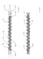
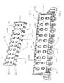
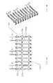
- the connector 12includes a plurality of wafer-like modules 42 (sometimes referred to herein as merely wafers). Each one of the modules 42 is configured to be received in a corresponding one of the slots 22 (FIG. 3).
- each one of the modules 42is identical in construction, an exemplary one thereof being shown in FIG. 4.
- Each one of such modules 42includes a dielectric support 44, shown more clearly in FIGS. 5 and 6.
- the dielectric support 44has a forward portion 46 and a pair of rearward, shoulder end portions 48.
- the forward portion 46is adapted in to inserted into a corresponding one of the slots 22.
- the shoulder end portions 48are configured to slide within a corresponding opposing pair of the grooves 39 (FIG. 3).
- the forward portion 46 of the dielectric support 44has substantially planar opposing surface portions 50, 52, as shown in FIGS. 5 and 6, respectively.
- the surface portion 50terminates along a beveled portion 54 disposed along a forward edge 56 of the dielectric support 44.
- the surface portion 52(FIG. 6) terminates along bevelled portions 58 interleaved with recesses 60 along the forward edge 56 of the dielectric support 44 to provide the support 44 with a spaced V-shaped forward edge 56.
- the module 42includes a plurality of signal electrical conductors 62 disposed in a linear array. More particularly, the signal conductors 62 are provided in a copper lead frame 64 (FIG. 7). The lead frame 64 is insert molded into the dielectric support 44, as shown in FIG. 5.
- portions 66 of the lead frame 64which are connected between the adjacent conductors 62, are cut away along edges 67 (FIGS. 5 and 6) to provide electrically isolated conductors 62, as shown in FIG. 5.
- Each one of )such signal electrical conductors 62has: a forward, beveled proximal end 68 (FIGS. 5 and 7) disposed along the forward edge 56 of the surface portion 50; and an elongated intermediate portion 70 connected between the proximal end 68 and a rearward, distal end 72 of the conductor 62.
- the intermediate portion 70 and the proximal end 68are partially embedded within the surface portion 50.
- the signal electrical conductors 62are electrically insulated one from another by interposed portions of the surface portion 50. It is noted that central, elongated, upper portions 74 of the intermediate portion 70 are raised, as a rib-shaped structure, above the surface 50 of the dielectric support 44, as shown more clearly in FIG. 8. This raised structure can be formed by coining the edges of the signal electrical conductors 62 before they are molded into dielectric support 44.
- the rearward, distal end 72includes a signal mounting pad 80 and a curved, here an arch-shaped, interconnect 82 disposed between an edge 83 of the signal mounting pad 80 and the intermediate portion 70.
- the interconnect 82is resilient and suspends the signal mounting pad 80 at the edge 83 thereof beyond a rearward edge 85 (FIGS. 5 and 6) of the surface portion 50 in a region between the pair of rearward shoulder end portions 48 and in a nominal orientation substantially perpendicular to the surface portion 50.
- An opposite edge 87 of the signal mounting pad 80being freely suspended outwardly from the surface portion 50.
- the mounting pads 80are adapted for soldering to pads, not shown, on the printed circuit board 16 (FIG. 1).
- the mounting padsmay be considered as contact tails.
- the pads 80are configured to accept "solder spheres" 81 (FIG. 4) as on Ball Grid Array (BGA) packages. If desired, the spheres 81 can be placed on the pad 80, and then fused to the pad using a surface mount solder reflow process. The resulting structure is shown in FIG. 4.
- Mounting pads 80can be shaped to facilitate attachment of a solder ball.
- FIG. 7shows pad 80 stamped with a dimple 86 in it. Dimple 86 leaves a bump on the upper surface of the pad but creates a concave lower surface. The concave surface forces the solder ball into the center of pad 80 during reflow. Positional accuracy of the solder ball is enhanced before the connector is attached to the printed circuit board. A similar result can be obtained by forming a hole in the pad 80.
- the shield member 84Disposed on the surface portion 52 (FIG. 6) of the dielectric support 44 is an electrical shielding member 84 as shown in FIG. 11.
- the shield member 84is copper and stamped as shown in FIG. 11.
- the shielding member 84includes a central region 88.
- the central region 88has holes 89 stamped therein and such holes 89 are press-fit onto posts 91 molded, and projecting outwardly from, the surface portion 50, as shown in FIG. 6.
- the shielding member 84has a forward plurality of openings 89 through which portion 58 (FIG. 6) of dielectric support 44 may project. Beveled portion 58 is insulative material backing the signal electrical conductors 68 thereby ensuring shield member 84 is not shorted to signal electrical conductors 68. Shielding member 84 has a beveled distal end 96 disposed in the recesses 60 (FIG. 6) along the forward edge 56 of the surface portion 52.
- the shielding member 84also includes a rearward plurality of electrical reference potential conductors 98 (FIG. 11) having: proximal ends 100 terminating along a rearward edge 102 of central region 88; reference potential mounting pads 104; and reference potential arch-shaped interconnects 105 disposed between an edge 106 of the reference potential mounting pads 104 and the rearward edge 102 of the central region 88.
- a rearward plurality of electrical reference potential conductors 98(FIG. 11) having: proximal ends 100 terminating along a rearward edge 102 of central region 88; reference potential mounting pads 104; and reference potential arch-shaped interconnects 105 disposed between an edge 106 of the reference potential mounting pads 104 and the rearward edge 102 of the central region 88.
- the reference potential arch-shaped interconnects 105are resilient and suspend the reference potential mounting pads 104 at the edges 106 thereof beyond a rearward edge of the surface portion 52 in a region between the pair of shoulder end portions 48 and in a nominal orientation substantially perpendicular to the surface portion 52 with an opposite edge 110 of the reference potential mounting pad 104 being freely-suspended outward from the surface portion 52.
- the reference potential mounting pads 104are freely suspended outward from the second surface portion 52 in a direction opposite to a direction of the suspended signal mounting pad 80 as shown in FIGS. 10 and 16.
- the mounting pads 104like pads 80, are adapted for soldering to surface mounting pads 300, 302 (FIGS.
- the pads 104are configured to accept "solder spheres" 107 (FIGS. 4, 9, and 10) as on Ball Grid Array (BGA) packages. If desired, the spheres can be placed on the pad 104, and then fused to the pad using a surface mount solder reflow process. The resulting structure is shown in FIG. 4 and 10.
- pads 104do not extend below the lower edge of shoulders 48. Thus, when a wafer is mounted on a board, pads 204 (FIG. 12A) will be held above the surface of the board. The area below pad 104 will be filled with solder-forming a solder joint. Thus, mating forces are shared by the housing and the solder joints.
- the plurality of signal mounting pads 80are disposed along a line 112 parallel to the rearward edge 85 of the dielectric support 44.
- the plurality of reference potential mounting pads 104are disposed along a line 114 parallel to the rearward edge 85, the lines 112, 114 being disposed on opposite sides of the dielectric support 44. Further, the reference potential mounting pads 104 are staggered with the signal mounting pads 80 along the rearward edge 85 of the dielectric support 44.
- the conductive region 88, the elongated intermediate portions 70 of signal conductors 62 and the dielectric member 44 disposed therebetweenare configured as microstrip transmission lines having a predetermined input impedance matched to the impedance of the printed circuit board 16, here an input impedance of 50 ohms.
- the length, L, (FIG. 5) of the transmission linesis easily extendable when longer modules are desired as for applications requiring greater height separation between the printed circuit boards 16, 18, FIG. 1. That is, the separation between boards 16, 18 is, in some applications, a function of the heat flow requirements between the boards 16, 18.
- the lengthis between 10 and 30 mm.
- the arch-shaped interconnects 82, 105are configured to provide an inductor.
- the pads 80, 104are here circular, or semi-circular shaped. These pads are attached to signal launches on a printed circuit board. The resulting interconnection will have a capacitive reactance. To counter-balance this capacitance the shape of the interconnects 82, 105 is selected to configure the interconnects 82, 105 as an inductor.
- the inductance of the interconnect 82, 105 and the capacitor of the pad 80, 104are serially connected and configured to provide a series resonant circuit with the result that a signal on one printed circuit board propagates through the series resonant circuit to the strip transmission line described above.
- the other connector 14is configured in a like manner so that the signal passes through an impedance matched microstrip transmission line therein and then through a similar series resonant circuit thereof.
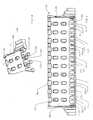
- the connector 14includes a dielectric, here plastic, housing 200.
- the housing 200has a plurality of parallel slots 202 formed in an upper surface 204 thereof.
- the slots 202extend longitudinally between opposing sides 206, 208 of the housing 200.
- the housing 200has a pair of opposing sidearms 210, 212 extending from the opposing sides 206, 208 in planes perpendicular to the slots 202.
- Each one of the sidearms 210, 212has disposed in surface portions thereof a plurality of grooves 214.
- Each one of the grooves 214 in each one of the sidearms 210, 212is aligned with a corresponding one of the slots 202 providing for each one of the slots 202 an opposing, aligned pair of the grooves 214.
- the housing 202has a pair of diagonally opposing mounting flanges 216, 218, each having a pair of holes therein for screws, or pins, not shown, which may be used to fasten or align the housing 200 to printed circuit board 18, FIG. 1.
- the sidewall 210has a post 211 for enabling the housing 200 to key with the slot 40 (FIG. 3) in the sidearm 30 of housing 20.
- the connector 14includes a plurality of wafer-like modules 230 (sometimes referred to herein as merely wafers). Each one of the modules 230 is identical in construction and is configured to be received in a corresponding one of the slots 202. An exemplary one of the modules 230 is shown in FIG. 13.
- Each one of the modules 230includes a dielectric support 232 having a forward portion 234 and a pair of rearward, shoulder end portions 236. The end portions 236 are configured to slide within a corresponding opposing pair of the grooves 214 (FIGS. 12A and 12B).
- the forward portion 234has substantially planar first and second opposing surfaces 240, shown in FIG. 13.
- the module 230includes a plurality of signal electrical conductors 242 disposed in a linear array. More particularly, the signal conductors 242 are provided in a copper lead frame 246 (FIGS. 15A, 15B).
- the lead frame 246is insert molded into the dielectric support 232 to form the structure shown in the right section of FIG. 13. When assembled, portions 249 of the lead frame 246 are cut away along edges 247 to provide electrically isolated conductors 242.
- Each one of the signal electrical conductors 242has a forward, proximal end 248 made up of: a first concave-shaped electrical contact 250; and, a resilient, cantilever beam, interconnect 252 (FIG. 14C) suspending the contact 250 beyond a forward edge of the dielectric support 232.
- the contact 250is adapted to have a forward portion 251 thereof engage the forward bevelled proximal end 68 (FIGS. 5 and 7) of a corresponding one of the plurality of signal electrical conductors 62 and bottom portions 253 thereof adapted to slide onto and electrically contact the central, elongated, upper rib portion 74 of the intermediate portion 70 of such corresponding one of the electrical signal conductors 62. That is, the raised, (i.e., upper), rib portion 74 has sufficient length to provide a full wipe along the bottom portion 253 of contact 250.
- Each one of the signal electrical conductors 242includes an intermediate portion 260 embedded in the dielectric support 232. Each one of such signal electrical conductors 242 is electrically insulated one from another by interposed portions of the dielectric support 232. A forward portion of the intermediate portion 260 is connected to the forward proximal end 248 of a corresponding one of the signal conductors 242. A rearward, distal end of each one of the signal electrical conductors 242 includes a signal mounting pad 262 and an arch-shaped interconnect 264 disposed between a rearward portion of the intermediate portion 260 and an edge 266 of the signal mounting pad 262.
- the interconnect 264is resilient and suspends the signal mounting pad 262 at the edge 266 thereof beyond the surface portion of the dielectric support 232 in a region between the pair of rearward shoulder end portions 236 and in a nominal orientation substantially perpendicular to the dielectric support 232 and with an opposite edge 268 of the signal pad 262 freely suspended outwardly from the dielectric support 232.
- the mounting pads 262are configured like the pads 80 and 104 are therefore adapted for soldering to surface mounting pads 300, 302 (FIG. 17, 18) on the printed circuit board 18 (FIG. 1). Further, the pads are configured to accept "solder spheres", not shown, as on Ball Grid Array (BGA) packages. If desired, the spheres can be placed on the pad, and then fused to the pad using a surface mount solder reflow process. Further, pads 262 and 292 are suspended in opposite directions as shown in FIG. 16.
- the module 230includes an electrical shielding )member 270 (FIG. 13).
- the electrical shielding member 270includes a conductive, ground plane plate 272 disposed on the surface 240 of the dielectric support 232.
- the plate 272has holes 273 stamped therein and such holes 273 are press-fit onto posts 275 molded, and projecting outwardly from, the surface 240, as shown in FIG. 13.
- the shielding member 270includes a forward plurality of electrical reference potential conductors 282 having rearward proximal ends terminating along a forward edge of the plate 272.
- Each one of the forward plurality of reference potential )conductors 282includes a concave-shaped electrical contact 284 and a resilient, cantilever beam, interconnect 286 suspending the contact 284 beyond a forward edge of the dielectric support 232.
- contact 284is adapted to make contact with beveled distal ends 96 of a corresponding one of the shielding members 84. the bottom portions 286 of the contacts 284 thereof slide onto and along the surface the conductive region 88 (FIGS. 9, 11, and 16).
- concave-shaped electrical contacts 250are wider than signal electrical conductors 62. Thus, good electrical contact is made even if there is some misalignment between modules 42 and 230.
- the concave electrical contacts 250, 282are staggered along the forward edge of the dielectric support 232, as shown in FIG 14B, and have a gap 291 therebetween to receive the forward, edge of the dielectric support 44 of module 42, as shown in FIG. 16.
- contacts 250are along line 320 and contacts 282 are along a parallel line 322, such lines 320, 322 being on opposite sides of dielectric support 232.
- the shielding member 270also includes a rearward plurality of electrical reference potential conductors 290.
- the electrical reference potential electrical conductors 290have proximal ends terminating along a rearward edge of the plate, reference potential mounting pads 292, and reference potential arch-shaped interconnects 294 disposed between an edge of the reference potential mounting pads and the rearward edge of the plate 272.
- the reference potential arch-shaped interconnects 294are resilient and suspending the reference potential mounting pads 292 at the edges thereof beyond said a rearward edge of the dielectric support 232 in a region between the pair of shoulder end portions 236 and in a nominal orientation substantially perpendicular to the dielectric support 232 with an opposite edge of the reference potential mounting pad being freely suspended outwardly from the second surface of the dielectric support 232 as with pads 80, 104 and 262.
- the plurality of reference potential mounting pads 292are identical in construction as pads 80, 104 and 262.
- the signal mounting pads 262are disposed along a line 295 parallel to the rearward edge of the dielectric support 236.
- the plurality of reference potential mounting pads 292are disposed along a line 296 parallel to the rearward edge of the dielectric support 236.
- the lines 295, 296are disposed on opposite sides of the dielectric support 236, as shown in FIG. 14A.
- the reference potential mounting pads 292are staggered with the signal mounting pads 262.
- center portions of arch-shaped interconnects 82 and the center portions of arch-shaped interconnects 105overlaying one another in region 297 (FIG. 16) to provide a degree of shielding of adjacent interconnects 82 (which are coupled to signal) in center portions of interconnects 105 (which are coupled to a reference potential, such as ground).
- each of the interconnects 82, 105, 264 and 294provides an inductor. It is also noted that the interconnects 82, 105, 264 and 294 also provide compliance to minimize mechanical stress on solder joints to the surface mounting pads 300, 302 (FIG. 17, 18) by lowering the effective moment of inertia in the contact area.
- the conductive plate 272(FIG. 13), the portions of signal conductors 242 embedded in the dielectric support 232 disposed therebetween are configured as microstrip transmission lines having an input impedance, here 50 ohms.
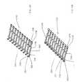
- the signal electrical conductors 62 and shielding member 84are provided to mate with the signal electrical conductors 242 and contacts 284 of the modules 230 (FIG. 1) in housing 14, respectively, as shown in FIG. 16.
- FIG. 17a layout of signal contact surface mounting pads 300 and ground contact surface mounting pads 302 for an exemplary one of the printed circuit boards 16, 18, here board 16, is shown.
- three rows 304, 306, 308, of contact surface mounting pads 300, 302are shown.
- Between each pair of adjacent rows 304, 306, or 306, 308are printed circuit board routing channels 311 (FIG. 18).
- FIG. 18There are four signal lines 310 in one layer of a printed circuit board which may be routed to the signal contact surface mounting pads 300.
- both the signal contact pads and the ground contact padsare disposed along rows, with the signal contact pads being interleaved with the ground contact pads, as indicated.
- the pads 80, 104, 262, and 292are preferably of semi-circular shape to facilitate the attachment of solder spheres and sized accordingly such that the sphere forms a cylinder or bulging sphere when reflow solder to the printed circuit board bridging the space between the pad and the surface mount pad on the printed circuit board.
- the cylindermay take a canted shape to allow the pad/surface mount pad misalignment.
- the conductorsmay optionally be coined on the underside to form a completely circular pad for attachment to the solder sphere reducing any tendency for the solder to wick up the conductor due to capillary action of solder wetting.
- the shoulder ends of the modulesare alignment indicia and have ears for retaining the modules in the housing.
- the housing, or shroudtransmits mating forces through the connectors 12 and 14 to boards 16 and 18, respectively. Thus, mating force shared by the housing or shroud and the solder joints.
- the modulesare retained in the housings only at their ends providing a degree of compliance across the span between sidewalls and the housing. Whereas each module is individually retained, a degree of compliance or independence is also achieved from module to module.
- modulesare retained in the direction across the shorter axis of the housing, parallel to the longitudinal axis of the housing to minimize any tendency to curt, or warp the housing as would be the case if the wafer were retained in the housing in the lengthwise, or elongated direction of the housing.
- wafers 42 and 230are held in support members with tabs inserted into slots thereby forming an interference fit.
- Other attachment methodscould be used.
- a snap fit connectionmight be used or metal barbs might be employed to provide a more secure connection if needed.
- the contact elementshave contact tails that are adapted for a surface mount connection.
- the connectormight be made with contact tails suitable for press-fit or through-hole connection.
- the disclosed embodimentshows a mezzanine type connector in which the signal contacts extend straight through wafers 42 and 230.
- it would be possible to make a right angle type connectorby bending the signal contacts at a right angle in region 260.
- Shield members 270would likewise be modified to have contacts 282 on an edge that is perpendicular to the edge carrying rearward electrical connectors 290.
- all wafers in each connector portionare shown to be the same. However, such is not required. For example, some wafers might be adapted for carrying power. For a power wafer the conductors might be made wider to have a higher current carrying capacity or some of the conductors could be made of different lengths to provide a mate-first-break-last connection. Still further, differential wafers might be formed by jogging pairs of signal contacts closer together.
- wafersare held together in a housing or shroud.
- a connectorcould be assembled without either or both pieces.
- wafer 42might be soldered directly to the printed circuit board 16 without the use of a shroud.
- all of the signal contacts in a waferare evenly spaced. It might be advantageous to tailor the spacing between signal contacts to provide a desired level of performance.
- cross-talk associated with signal contacts at the end of a columnis sometimes greater than the cross-talk associated with contacts at the center of a column.
- the performance of the connectoris more balanced-meaning that all contacts have similar performance.
- FIG. 19Aillustrates this construction. Comparing FIG. 19A to FIG. 15A, the intermediate portion 260A of the signal contacts at the end of the column are spaced from the intermediate portion 260 at the end of the next nearest signal contact by a distance D.. In contrast, the intermediate portions 260 in the center of the connector have a spacing of D 1 . Here, D 2 is larger than D 1 .
- FIG. 19Ashows the spacing between pads 262 and contacts 250 is uniform. This arrangement is provided by jogs in the intermediate portions 260A.
- FIG. 19Bshows a similar jogged arrangement for the signal contacts in wafer 42. Comparing FIG. 7 to FIG. 19B, it can be seen that FIG. 19B illustrates an embodiment in which the intermediate portions of the end signal contacts are jogged away from the intermediate portion of the nearest signal contact.
- a connectorshould be rated based on performance of the signal contact with the lowest performance tailoring the performance of one or two low performing signal contacts can increase the rated performance of the entire connector.
- the spacing between ground and signal contactswas selected to exactly match the impedance of signal traces in the printed circuit board. This spacing might be reduced to reduce cross-talk between adjacent signal conductors. Alternatively, the spacing might be adjusted to provide other impedances, which could be desired in other applications. The spacing, as well as the dimensions in the connector, will likely be set based on results of computer simulation and testing to provide performance levels suited for a given application.
- wafersare made with signal contacts on one side and ground contacts on the other. It might be desirable to have signal contacts on both sides of a wafer. Such a construction might be very useful for carrying differential signals.
- the end ones of the pads 104 and the interconnects 105 connected to such end pads 104 of shielding member 84may be removed.
- the end ones of the pads 292 and the interconnects 294 connected to such end pads 292 of shielding member 270may be removed.
Landscapes
- Details Of Connecting Devices For Male And Female Coupling (AREA)
- Coupling Device And Connection With Printed Circuit (AREA)
- Connector Housings Or Holding Contact Members (AREA)
- Cable Accessories (AREA)
Abstract
Description
This invention relates generally to electricalconnectors and more particular to very high densityelectrical connectors adapted for use with printed circuitboards.
As is known in the art, electrical connectors ofthe type used with printed circuit boards are becomingsmaller and are required to operate with data signalshaving extremely short edge rise times. Further, suchconnectors must be mechanically robust and configured toenable relatively low manufacturing cost.
In accordance with one feature of the invention, anelectrical connector is provided having a plurality ofelectrical conductors with portions thereof disposed in ahousing and ends thereof terminating in pads orientedperpendicular to the housing disposed portions of theconductors.
In a preferred embodiment, solder balls aredisposed on the pads to facilitate mounting to a printedcircuit board.
In accordance with another feature of theinvention, the pad is coupled to the conductor through acurved interconnect. The interconnect is configured as aninductor to provide a series resonant circuit element forcapacitance provided by the pad and attachment to theprinted circuit board.
In accordance with another feature of theinvention, an electrical connector is provided having ahousing adapted to have therein a plurality of wafer-likemodules. Each one of the modules has a dielectric supportand an array of signal electrical conductors electricallyinsulated one from another by portions of the support. A ground plane electrical conductor is provided. The groundplane conductor is disposed under, and is separated from,portions of the signal electrical conductor by thedielectric member. The signal conductor, ground planeconductor, and portion of the dielectric support membertherebetween are configured as a microstrip transmissionline having a predetermined impedance.
With such an arrangement, the microstriptransmission line extends along a length of the connectorin a region between an overlaying pair of printed circuitboards. Thus, the microstrip transmission line in theconnector appears the same as, i.e., is matched to, thetransmission line in the printed circuit board. Therefore,once the connector is designed, the length of themicrostrip transmission line can be readily extended tosimilar connectors having different lengths to accommodateddifferent height separation requirements between theoverlying printed circuit boards.
These and other feature of the invention, as wellas the invention itself, will become more readily apparentfrom the following detailed description when read togetherwith the following drawings, in which:
Referring now to FIGS. 1 and 2, anelectricalconnector assembly 10 is shown. Theassembly 10 includes apair of moldedelectrical connectors connector 12, is adapted formounting to a first printedcircuit board 16 and the otherelectrical connector 14 is adapted for mounting to a secondprintedcircuit board 18 positioned parallel to, herebelow, the first printedcircuit board 12.
Referring now also to FIG. 3,connector 12 includesa dielectric, here plastic,housing 20, here a shroud,having a plurality ofparallel slots 22 formed in anuppersurface 24 thereof. Theslots 22 extend betweenopposingsides 26, 28 of thehousing 20. Thehousing 20 has a pairofopposing sidearms opposingsides 26, 28 in planes perpendicular to theslots 22.Housing 20 has disposed in an undersurface thereof a plurality ofgrooves 39. Each one of thegrooves 39 isaligned with a corresponding one of theslots 22 providingfor each one of theslots 22 an opposing, aligned pair ofthegrooves 39. Thehousing 20 has a pair of diagonallyopposingmounting flanges sidewall 30 has aslot 40 forenabling thehousing 20 to key with a post, to bedescribed, in the housing ofconnector 14.
Referring again to FIG. 1, theconnector 12includes a plurality of wafer-like modules 42 (sometimesreferred to herein as merely wafers). Each one of themodules 42 is configured to be received in a correspondingone of the slots 22 (FIG. 3). In the preferred embodiment,each one of themodules 42 is identical in construction, anexemplary one thereof being shown in FIG. 4. Each one ofsuch modules 42 includes adielectric support 44, shownmore clearly in FIGS. 5 and 6. Thedielectric support 44has aforward portion 46 and a pair of rearward,shoulderend portions 48. Theforward portion 46 is adapted in toinserted into a corresponding one of theslots 22. Theshoulder end portions 48 are configured to slide within acorresponding opposing pair of the grooves 39 (FIG. 3).Theforward portion 46 of thedielectric support 44 hassubstantially planar opposingsurface portions surface portion 50 terminates along abeveled portion 54 disposed along aforward edge 56 of thedielectric support 44. The surfaceportion 52 (FIG. 6) terminates along bevelledportions 58interleaved withrecesses 60 along theforward edge 56 ofthedielectric support 44 to provide thesupport 44 with aspaced V-shapedforward edge 56.
Themodule 42 includes a plurality of signalelectrical conductors 62 disposed in a linear array. Moreparticularly, thesignal conductors 62 are provided in acopper lead frame 64 (FIG. 7). Thelead frame 64 is insertmolded into thedielectric support 44, as shown in FIG. 5.
When assembled,portions 66 of thelead frame 64, whichare connected between theadjacent conductors 62, are cutaway along edges 67 (FIGS. 5 and 6) to provide electricallyisolatedconductors 62, as shown in FIG. 5. Each one of)such signalelectrical conductors 62 has: a forward,beveled proximal end 68 (FIGS. 5 and 7) disposed along theforward edge 56 of thesurface portion 50; and an elongatedintermediate portion 70 connected between theproximal end 68 and a rearward,distal end 72 of theconductor 62. Theintermediate portion 70 and theproximal end 68 arepartially embedded within thesurface portion 50. As notedabove, the signalelectrical conductors 62 are electricallyinsulated one from another by interposed portions of thesurface portion 50. It is noted that central, elongated,upper portions 74 of theintermediate portion 70 areraised, as a rib-shaped structure, above thesurface 50 ofthedielectric support 44, as shown more clearly in FIG. 8.This raised structure can be formed by coining the edgesof the signalelectrical conductors 62 before they aremolded intodielectric support 44.
The rearward,distal end 72 includes asignalmounting pad 80 and a curved, here an arch-shaped,interconnect 82 disposed between anedge 83 of thesignalmounting pad 80 and theintermediate portion 70. Theinterconnect 82 is resilient and suspends thesignalmounting pad 80 at theedge 83 thereof beyond a rearwardedge 85 (FIGS. 5 and 6) of thesurface portion 50 in aregion between the pair of rearwardshoulder end portions 48 and in a nominal orientation substantially perpendicularto thesurface portion 50. Anopposite edge 87 of thesignal mounting pad 80 being freely suspended outwardlyfrom thesurface portion 50. The mountingpads 80 areadapted for soldering to pads, not shown, on the printedcircuit board 16 (FIG. 1). It should be noted that themounting pads may be considered as contact tails.) Thepads 80 are configured to accept "solder spheres" 81 (FIG.4) as on Ball Grid Array (BGA) packages. If desired, thespheres 81 can be placed on thepad 80, and then fused tothe pad using a surface mount solder reflow process. Theresulting structure is shown in FIG. 4.
Mountingpads 80 can be shaped to facilitateattachment of a solder ball. FIG. 7 showspad 80 stampedwith adimple 86 in it.Dimple 86 leaves a bump on theupper surface of the pad but creates a concave lowersurface. The concave surface forces the solder ball intothe center ofpad 80 during reflow. Positional accuracy ofthe solder ball is enhanced before the connector isattached to the printed circuit board. A similar resultcan be obtained by forming a hole in thepad 80.
Disposed on the surface portion 52 (FIG. 6) of thedielectric support 44 is anelectrical shielding member 84as shown in FIG. 11. Theshield member 84 is copper andstamped as shown in FIG. 11. The shieldingmember 84includes acentral region 88. Thecentral region 88 hasholes 89 stamped therein andsuch holes 89 are press-fitontoposts 91 molded, and projecting outwardly from, thesurface portion 50, as shown in FIG. 6.
The shieldingmember 84 has a forward plurality ofopenings 89 through which portion 58 (FIG. 6) ofdielectricsupport 44 may project. Beveledportion 58 is insulativematerial backing the signalelectrical conductors 68 thereby ensuringshield member 84 is not shorted to signalelectrical conductors 68. Shieldingmember 84 has abeveleddistal end 96 disposed in the recesses 60 (FIG. 6)along theforward edge 56 of thesurface portion 52.
The shieldingmember 84 also includes a rearwardplurality of electrical reference potential conductors 98(FIG. 11) having: proximal ends 100 terminating along arearward edge 102 ofcentral region 88; referencepotentialmounting pads 104; and reference potential arch-shapedinterconnects 105 disposed between an edge 106 of thereferencepotential mounting pads 104 and therearward edge 102 of thecentral region 88. The reference potentialarch-shapedinterconnects 105, likeinterconnects 82, areresilient and suspend the referencepotential mounting pads 104 at the edges 106 thereof beyond a rearward edge of thesurface portion 52 in a region between the pair ofshoulderend portions 48 and in a nominal orientation substantiallyperpendicular to thesurface portion 52 with anoppositeedge 110 of the referencepotential mounting pad 104 beingfreely-suspended outward from thesurface portion 52.Thus, it is noted that the referencepotential mountingpads 104 are freely suspended outward from thesecondsurface portion 52 in a direction opposite to a directionof the suspendedsignal mounting pad 80 as shown in FIGS.10 and 16. The mountingpads 104, likepads 80, areadapted for soldering to surface mountingpads 300, 302(FIGS. 17, 18) on the printed circuit board 16 (FIG. 1).Thepads 104, likepads 80, are configured to accept"solder spheres" 107 (FIGS. 4, 9, and 10) as on Ball GridArray (BGA) packages. If desired, the spheres can beplaced on thepad 104, and then fused to the pad using asurface mount solder reflow process. The resultingstructure is shown in FIG. 4 and 10.
It should be noted that thepads 104 do not extendbelow the lower edge ofshoulders 48. Thus, when a waferis mounted on a board, pads 204 (FIG. 12A) will be heldabove the surface of the board. The area belowpad 104will be filled with solder-forming a solder joint. Thus,mating forces are shared by the housing and the solderjoints.
Referring also to FIG. 5B, the plurality ofsignalmounting pads 80 are disposed along aline 112 parallel totherearward edge 85 of thedielectric support 44. Theplurality of referencepotential mounting pads 104 aredisposed along aline 114 parallel to therearward edge 85,thelines dielectric support 44. Further, the referencepotentialmounting pads 104 are staggered with thesignal mountingpads 80 along therearward edge 85 of thedielectricsupport 44.
Referring to again to FIG. 8, it should be notedthat theconductive region 88, the elongatedintermediateportions 70 ofsignal conductors 62 and thedielectricmember 44 disposed therebetween are configured asmicrostrip transmission lines having a predetermined inputimpedance matched to the impedance of the printedcircuitboard 16, here an input impedance of 50 ohms. It is alsonoted that the length, L, (FIG. 5) of the transmissionlines is easily extendable when longer modules are desiredas for applications requiring greater height separationbetween the printedcircuit boards boards boards
It should also be noted that the arch-shapedinterconnects pads interconnects interconnects interconnect pad other connector 14 isconfigured in a like manner so that the signal passesthrough an impedance matched microstrip transmission linetherein and then through a similar series resonant circuitthereof.
Referring again to FIG. 1, theconnector 14includes a dielectric, here plastic,housing 200.Referring also to FIGS. 12A and 12B, thehousing 200 has aplurality ofparallel slots 202 formed in anupper surface 204 thereof. Theslots 202 extend longitudinally betweenopposingsides housing 200. Thehousing 200 has a pair of opposingsidearms sides slots 202. Each one of thesidearms grooves 214.Each one of thegrooves 214 in each one of thesidearms slots 202 providing for each one of theslots 202 an opposing,aligned pair of thegrooves 214. Thehousing 202 has apair of diagonally opposing mountingflanges housing 200to printedcircuit board 18, FIG. 1. Thesidewall 210 hasapost 211 for enabling thehousing 200 to key with theslot 40 (FIG. 3) in thesidearm 30 ofhousing 20.
Referring now also to FIG. 1, theconnector 14includes a plurality of wafer-like modules 230 (sometimesreferred to herein as merely wafers). Each one of themodules 230 is identical in construction and is configuredto be received in a corresponding one of theslots 202. Anexemplary one of themodules 230 is shown in FIG. 13. Eachone of themodules 230 includes adielectric support 232having aforward portion 234 and a pair of rearward,shoulder end portions 236. Theend portions 236 areconfigured to slide within a corresponding opposing pair ofthe grooves 214 (FIGS. 12A and 12B). Theforward portion 234 has substantially planar first and second opposingsurfaces 240, shown in FIG. 13. Themodule 230 includes aplurality of signalelectrical conductors 242 disposed in alinear array. More particularly, thesignal conductors 242are provided in a copper lead frame 246 (FIGS. 15A, 15B).Thelead frame 246 is insert molded into thedielectricsupport 232 to form the structure shown in the rightsection of FIG. 13. When assembled,portions 249 of thelead frame 246 are cut away alongedges 247 to provideelectrically isolatedconductors 242. Each one of thesignalelectrical conductors 242 has a forward,proximalend 248 made up of: a first concave-shapedelectricalcontact 250; and, a resilient, cantilever beam, interconnect 252 (FIG. 14C) suspending thecontact 250beyond a forward edge of thedielectric support 232. Thecontact 250 is adapted to have aforward portion 251thereof engage the forward bevelled proximal end 68 (FIGS.5 and 7) of a corresponding one of the plurality of signalelectrical conductors 62 andbottom portions 253 thereofadapted to slide onto and electrically contact the central,elongated,upper rib portion 74 of theintermediate portion 70 of such corresponding one of theelectrical signalconductors 62. That is, the raised, (i.e., upper),ribportion 74 has sufficient length to provide a full wipealong thebottom portion 253 ofcontact 250.
Each one of the signalelectrical conductors 242includes anintermediate portion 260 embedded in thedielectric support 232. Each one of such signalelectricalconductors 242 is electrically insulated one from anotherby interposed portions of thedielectric support 232. Aforward portion of theintermediate portion 260 isconnected to the forwardproximal end 248 of acorresponding one of thesignal conductors 242. Arearward, distal end of each one of the signalelectricalconductors 242 includes asignal mounting pad 262 and anarch-shapedinterconnect 264 disposed between a rearwardportion of theintermediate portion 260 and anedge 266 ofthesignal mounting pad 262. Theinterconnect 264 isresilient and suspends thesignal mounting pad 262 at theedge 266 thereof beyond the surface portion of thedielectric support 232 in a region between the pair ofrearwardshoulder end portions 236 and in a nominalorientation substantially perpendicular to thedielectricsupport 232 and with anopposite edge 268 of thesignal pad 262 freely suspended outwardly from thedielectric support 232. The mountingpads 262 are configured like thepads pads 300, 302 (FIG. 17, 18) on the printed circuitboard 18 (FIG. 1). Further, the pads are configured toaccept "solder spheres", not shown, as on Ball Grid Array(BGA) packages. If desired, the spheres can be placed onthe pad, and then fused to the pad using a surface mountsolder reflow process. Further,pads
Themodule 230 includes an electrical shielding)member 270 (FIG. 13). Theelectrical shielding member 270includes a conductive,ground plane plate 272 disposed onthesurface 240 of thedielectric support 232. Theplate 272 hasholes 273 stamped therein andsuch holes 273 arepress-fit ontoposts 275 molded, and projecting outwardlyfrom, thesurface 240, as shown in FIG. 13. The shieldingmember 270 includes a forward plurality of electricalreferencepotential conductors 282 having rearward proximalends terminating along a forward edge of theplate 272.Each one of the forward plurality of reference potential)conductors 282 includes a concave-shapedelectrical contact 284 and a resilient, cantilever beam,interconnect 286suspending thecontact 284 beyond a forward edge of thedielectric support 232. During mating ofconnectors contact 284 is adapted to make contact with beveleddistal ends 96 of a corresponding one of the shieldingmembers 84. thebottom portions 286 of thecontacts 284thereof slide onto and along the surface the conductiveregion 88 (FIGS. 9, 11, and 16).
Also, it should be noted that concave-shapedelectrical contacts 250 are wider than signalelectricalconductors 62. Thus, good electrical contact is made evenif there is some misalignment betweenmodules
The concaveelectrical contacts dielectric support 232, as shown in FIG 14B, and have agap 291 therebetweento receive the forward, edge of thedielectric support 44ofmodule 42, as shown in FIG. 16. Thus,contacts 250 arealongline 320 andcontacts 282 are along aparallel line 322,such lines dielectric support 232.
The shieldingmember 270 also includes a rearwardplurality of electrical referencepotential conductors 290.
The electrical reference potentialelectrical conductors 290 have proximal ends terminating along a rearward edge ofthe plate, referencepotential mounting pads 292, andreference potential arch-shapedinterconnects 294 disposedbetween an edge of the reference potential mounting padsand the rearward edge of theplate 272. The referencepotential arch-shapedinterconnects 294 are resilient andsuspending the referencepotential mounting pads 292 at theedges thereof beyond said a rearward edge of thedielectricsupport 232 in a region between the pair ofshoulder endportions 236 and in a nominal orientation substantiallyperpendicular to thedielectric support 232 with anopposite edge of the reference potential mounting pad beingfreely suspended outwardly from the second surface of thedielectric support 232 as withpads potential mounting pads 292 areidentical in construction aspads signal mounting pads 262 are disposed along aline 295parallel to the rearward edge of thedielectric support 236. The plurality of referencepotential mounting pads 292are disposed along aline 296 parallel to the rearward edgeof thedielectric support 236. Thelines dielectric support 236, as shown in FIG. 14A. The referencepotential mountingpads 292 are staggered with thesignal mounting pads 262.
Further, it should be noted that center portions ofarch-shapedinterconnects 82 and the center portions ofarch-shapedinterconnects 105 overlaying one another inregion 297 (FIG. 16) to provide a degree of shielding ofadjacent interconnects 82 (which are coupled to signal) incenter portions of interconnects 105 (which are coupled toa reference potential, such as ground). In like manner, itis noted that center portions of arch-shapedinterconnects 264 and the center portions of arch-shapedinterconnects 294 overlaying one another in region 298 (FIG. 16) toprovide a degree of shielding of adjacent interconnects 264(which are coupled to signal) in center portions ofinterconnects 294 (which are coupled to a referencepotential, such as ground). As noted above, each of theinterconnects interconnects surface mounting pads 300, 302(FIG. 17, 18) by lowering the effective moment of inertiain the contact area.
Referring to FIG. 14C, it is noted that theconductive plate 272 (FIG. 13), the portions ofsignalconductors 242 embedded in thedielectric support 232disposed therebetween are configured as microstriptransmission lines having an input impedance, here 50 ohms.
It is also noted that when themodules 42 aredisposed inhousing 12, as shown in FIG. 2, the signalelectrical conductors 62 and shieldingmember 84 areprovided to mate with the signalelectrical conductors 242andcontacts 284 of the modules 230 (FIG. 1) inhousing 14,respectively, as shown in FIG. 16.
Referring now to FIG. 17, a layout of signalcontactsurface mounting pads 300 and ground contactsurface mounting pads 302 for an exemplary one of theprintedcircuit boards board 16, is shown.Here, threerows surface mountingpads adjacentrows signal lines 310 in one layer of a printedcircuit board which may be routed to the signal contactsurface mounting pads 300. Thus, it is noted that both thesignal contact pads and the ground contact pads aredisposed along rows, with the signal contact pads beinginterleaved with the ground contact pads, as indicated.
It should be noted that thepads
The shoulder ends of the modules are alignmentindicia and have ears for retaining the modules in thehousing. The housing, or shroud, transmits mating forcesthrough theconnectors boards
Other embodiments are within the spirit and scopeof the appended claims. For example, it is described thatwafers
Also, it was described that the contact elementshave contact tails that are adapted for a surface mountconnection. The connector might be made with contact tailssuitable for press-fit or through-hole connection.
Moreover, the disclosed embodiment shows amezzanine type connector in which the signal contactsextend straight throughwafers region 260.
Further, in the preferred embodiment, all wafers ineach connector portion are shown to be the same. However,such is not required. For example, some wafers might beadapted for carrying power. For a power wafer the conductors might be made wider to have a higher currentcarrying capacity or some of the conductors could be madeof different lengths to provide a mate-first-break-lastconnection. Still further, differential wafers might beformed by jogging pairs of signal contacts closer together.
Further, the preferred embodiment has beendescribed in which wafers are held together in a housing orshroud. A connector could be assembled without either orboth pieces. For example,wafer 42 might be soldereddirectly to the printedcircuit board 16 without the use ofa shroud.
Moreover, it is pictured in the illustratedembodiment that all of the signal contacts in a wafer areevenly spaced. It might be advantageous to tailor thespacing between signal contacts to provide a desired levelof performance. In particular, cross-talk associated withsignal contacts at the end of a column is sometimes greaterthan the cross-talk associated with contacts at the centerof a column. Thus, by increasing the spacing between theend contacts and the next nearest contact, the performanceof the connector is more balanced-meaning that all contactshave similar performance.
It is not necessary that all portions of the endcontacts be positioned farther from the adjacent signalcontact. In some instances, it will be desirable to havethe contact tails and the mating portions of the contactson a uniform pitch. Thus, it is only the intermediateportions of the contacts that are offset. FIG. 19Aillustrates this construction. Comparing FIG. 19A to FIG.15A, theintermediate portion 260A of the signal contactsat the end of the column are spaced from theintermediateportion 260 at the end of the next nearest signal contactby a distance D.. In contrast, theintermediate portions 260 in the center of the connector have a spacing of D1.Here, D2 is larger than D1.
Nonetheless, FIG. 19A shows the spacing betweenpads 262 andcontacts 250 is uniform. This arrangement isprovided by jogs in theintermediate portions 260A.
FIG. 19B shows a similar jogged arrangement for thesignal contacts inwafer 42. Comparing FIG. 7 to FIG. 19B,it can be seen that FIG. 19B illustrates an embodiment inwhich the intermediate portions of the end signal contactsare jogged away from the intermediate portion of thenearest signal contact.
Because a connector should be rated based onperformance of the signal contact with the lowestperformance tailoring the performance of one or two lowperforming signal contacts can increase the ratedperformance of the entire connector.
Also, it was described that the spacing betweenground and signal contacts was selected to exactly matchthe impedance of signal traces in the printed circuitboard. This spacing might be reduced to reduce cross-talkbetween adjacent signal conductors. Alternatively, thespacing might be adjusted to provide other impedances,which could be desired in other applications. The spacing,as well as the dimensions in the connector, will likely beset based on results of computer simulation and testing toprovide performance levels suited for a given application.
As a still alternative, it is described that wafersare made with signal contacts on one side and groundcontacts on the other. It might be desirable to havesignal contacts on both sides of a wafer. Such aconstruction might be very useful for carrying differentialsignals.
Further, referring to FIG. 11, the end ones of thepads 104 and theinterconnects 105 connected tosuch end pads 104 of shieldingmember 84 may be removed. Likewise, referring to FIG. 13, the end ones of thepads 292 and theinterconnects 294 connected tosuch end pads 292 of shieldingmember 270may be removed.
Other features of the invention are set forth in the following numberedparagraphs.
Claims (16)
- An electrical connector comprising:a housing having a plurality of parallel slots;a plurality of wafers, each of the plurality of wafers being configured to bereceived by one of the plurality of parallel slots of the housing;each of the plurality of wafers including a plurality of signal conductors, each ofthe plurality of signal conductors having an end portion;each of the plurality of wafers providing a reference potential through referencepotential end portions;a solder ball connected to each of the signal conductor end portions andreference potential end portions, wherein the solder balls connected to the signalconductor end portions and the reference potential end portions lie along a commonplane; andfor each of the plurality of wafers, the signal conductor end portions are bent in afirst direction such that the solder balls connected thereto are aligned along a first line,and the reference potential end portions are bent in a second direction, opposite from thefirst direction, such that the solder balls connected thereto are aligned along a secondline.
- The electrical connector of claim 1, wherein each of the plurality of wafersfurther comprises an insulative support securing the plurality of signal conductors, theinsulative support having a first side and a second side.
- The electrical connector of claim 2, wherein the signal conductor end portionsfor each of the plurality of wafers extend from the first end of the insulative support.
- The electrical connector of claim 3, wherein each of the plurality of signalconductors further comprises a contact portion extending from the second side of theinsulative support.
- The electrical connector of claim 4, wherein the contact portion of each of theplurality of signal conductors comprises a compliant beam extending from the secondside of the insulative support perpendicular to the common plane of the solder balls.
- The electrical connector of claim 1, wherein for each of the plurality of wafers,the signal conductor end portions and the reference potential end portions areinterleaved.
- The electrical connector of claim 1, wherein the plurality of wafers are identicalto one another.
- The electrical connector of claim 1, wherein the first line and the second line areparallel.
- An electrical connector assembly comprising:a first connector for mounting on a first printed circuit board, the first connectorcomprising:a first housing having a plurality of parallel slots;a plurality of first wafers, each of the plurality of first wafers being configured tobe received by one of the plurality of parallel slots of the first housing;each of the plurality of first wafers including a plurality of first signalconductors, each of the plurality of first signal conductors having an end portion and acontact portion;each of the plurality of first wafers also including a first insulative supportsecuring the plurality of first signal conductors, the first insulative support having a firstside and a second side, wherein the first signal conductor end portions extend from thefirst side and the first signal conductor contact portions extend from the second side;each of the end portions of the plurality of first signal conductors having a padconfigured to accept a solder ball, wherein the solder balls connected to the first signalconductor end portions lie along a first plane; andfor each of the plurality of first wafers, the first signal conductor end portionsare bent such that the solder balls disposed thereon are aligned along a line;a second connector for mounting on a second printed circuit board, the secondconnector mateable with the first connector, comprising;a second housing having a plurality of parallel slots;a plurality of second wafers, each of the plurality of second wafers beingconfigured to be received by one of the plurality of parallel slots of the second housing;each of the plurality of second wafers including a plurality of second signalconductors, each of the plurality of second signal conductors having an end portion anda contact portion;each of the plurality of second wafers also including a second insulative supportsecuring the plurality of second signal conductors, the second insulative support havinga first side and a second side, wherein the second signal conductor end portions extendfrom the first side and the second signal conductor contact portions extend from thesecond side;each of the end portions of the plurality of second signal conductors having apad configured to accept a solder ball, wherein the solder balls connected to the secondsignal conductor end portions lie along a second plane; andfor each of the plurality of second wafers, the second signal conductor endportions are bent such that the solder balls disposed thereon are aligned along a line.
- The electrical connector assembly of claim 9, wherein:each of the plurality of first wafers provides a reference potential through aplurality of first reference potential end portions and each of the plurality of secondwafers provides a reference potential through a plurality of second reference potentialend portions; anda solder ball connected to each of the first reference potential end portions andsecond reference potential end portions, wherein the solder balls connected to the firstreference potential end portions lie along the first plane and the solder balls connectedto the second reference potential end portions lie along the second plane.
- The electrical connector assembly of claim 10, wherein for each of the pluralityof first wafers, the first signal conductor end portions and the first reference potentialend portions are interleaved.
- The electrical connector assembly of claim 9, wherein the contact portion ofeach of the plurality of first signal conductors comprises a compliant beam extendingfrom the second side of the first insulative support perpendicular to the first plane of thesolder balls, and the contact portion of each of the plurality of second signal conductorscomprises a compliant beam extending from the second side of the second insulativesupport perpendicular to the second plane of the solder balls.
- The electrical connector assembly of claim 9, wherein the plurality of firstwafers are identical to one another and the plurality of second wafers are identical toone another.
- An electrical connector assembly comprising:a first connector for mounting on a first printed circuit board, the first connectorcomprising:wherein the first wafers are aligned in parallel, the first solder balls lie ina first plane and the contact portions of the first conductive members are perpendicularto the first plane;a plurality of first wafers, each of the first wafers having a first insulativesupport and a plurality of first conductive members secured therein, each of the firstconductive members having an end portion extending from the first insulative supportand a contact portion extending from the first insulative support;each of the end portions of the plurality of first conductive membershaving a pad configured to accept a first solder ball; anda second connector for mounting on a second printed circuit board, thesecond connector mateable with the first connector, comprising:wherein the second wafers are aligned in parallel, the second solder ballslie in a second plane and the contact portions of the second conductive members areperpendicular to the second plane.a plurality of second wafers, each of the second wafers having a secondinsulative support and a plurality of second conductive members secured therein, eachof the second conductive members having an end portion extending from the secondinsulative support and a contact portion extending from the second insulative support;each of the end portions of the plurality of second conductive membershaving a pad configured to accept a second solder ball; and
- The electrical connector assembly of claim 14, wherein the first wafersare identical to one another and the second wafers are identical to one another.
- An electrical connector, comprising: a housing; a plurality ofelectrical conductors having portions thereof disposed in the housing and ends thereofconnected to contact tails adapted for attachment to a printed circuit board; and solderdisposed on the contact tails.
Applications Claiming Priority (3)
| Application Number | Priority Date | Filing Date | Title |
|---|---|---|---|
| US198422 | 1998-11-24 | ||
| US09/198,422US6530790B1 (en) | 1998-11-24 | 1998-11-24 | Electrical connector |
| EP99965861AEP1133812B1 (en) | 1998-11-24 | 1999-11-22 | High density electrical connector |
Related Parent Applications (2)
| Application Number | Title | Priority Date | Filing Date |
|---|---|---|---|
| EP99965861ADivisionEP1133812B1 (en) | 1998-11-24 | 1999-11-22 | High density electrical connector |
| EP99965861ADivision-IntoEP1133812B1 (en) | 1998-11-24 | 1999-11-22 | High density electrical connector |
Publications (2)
| Publication Number | Publication Date |
|---|---|
| EP1411594A2true EP1411594A2 (en) | 2004-04-21 |
| EP1411594A3 EP1411594A3 (en) | 2009-01-28 |
Family
ID=22733320
Family Applications (2)
| Application Number | Title | Priority Date | Filing Date |
|---|---|---|---|
| EP04000082AWithdrawnEP1411594A3 (en) | 1998-11-24 | 1999-11-22 | High density electrical connector |
| EP99965861AExpired - LifetimeEP1133812B1 (en) | 1998-11-24 | 1999-11-22 | High density electrical connector |
Family Applications After (1)
| Application Number | Title | Priority Date | Filing Date |
|---|---|---|---|
| EP99965861AExpired - LifetimeEP1133812B1 (en) | 1998-11-24 | 1999-11-22 | High density electrical connector |
Country Status (8)
| Country | Link |
|---|---|
| US (2) | US6530790B1 (en) |
| EP (2) | EP1411594A3 (en) |
| JP (3) | JP4039808B2 (en) |
| CN (1) | CN1127780C (en) |
| AT (1) | ATE263441T1 (en) |
| AU (1) | AU2154500A (en) |
| DE (1) | DE69916100T2 (en) |
| WO (1) | WO2000031832A1 (en) |
Cited By (1)
| Publication number | Priority date | Publication date | Assignee | Title |
|---|---|---|---|---|
| US20230155328A1 (en)* | 2020-04-08 | 2023-05-18 | Samtec, Inc. | High-speed electrical connector |
Families Citing this family (160)
| Publication number | Priority date | Publication date | Assignee | Title |
|---|---|---|---|---|
| US6406316B1 (en) | 1998-01-31 | 2002-06-18 | Fci Americas Technology, Inc. | Electrical connector with multiple housings |
| US6869292B2 (en)* | 2001-07-31 | 2005-03-22 | Fci Americas Technology, Inc. | Modular mezzanine connector |
| US7390200B2 (en)* | 2001-11-14 | 2008-06-24 | Fci Americas Technology, Inc. | High speed differential transmission structures without grounds |
| US6994569B2 (en)* | 2001-11-14 | 2006-02-07 | Fci America Technology, Inc. | Electrical connectors having contacts that may be selectively designated as either signal or ground contacts |
| CN100483886C (en)* | 2001-11-14 | 2009-04-29 | Fci公司 | Crosstalk reduction for electrical connectors |
| US6981883B2 (en) | 2001-11-14 | 2006-01-03 | Fci Americas Technology, Inc. | Impedance control in electrical connectors |
| US6667225B2 (en)* | 2001-12-17 | 2003-12-23 | Intel Corporation | Wafer-bonding using solder and method of making the same |
| US6764349B2 (en)* | 2002-03-29 | 2004-07-20 | Teradyne, Inc. | Matrix connector with integrated power contacts |
| US6638079B1 (en)* | 2002-05-21 | 2003-10-28 | Hon Hai Precision Ind. Co., Ltd. | Customizable electrical connector |
| US6743049B2 (en) | 2002-06-24 | 2004-06-01 | Advanced Interconnections Corporation | High speed, high density interconnection device |
| US6808399B2 (en)* | 2002-12-02 | 2004-10-26 | Tyco Electronics Corporation | Electrical connector with wafers having split ground planes |
| US7242592B2 (en)* | 2003-06-24 | 2007-07-10 | Amphenol Corporation | Printed circuit board for high speed, high density electrical connector with improved cross-talk minimization, attenuation and impedance mismatch characteristics |
| US6814619B1 (en)* | 2003-06-26 | 2004-11-09 | Teradyne, Inc. | High speed, high density electrical connector and connector assembly |
| US6780059B1 (en)* | 2003-06-26 | 2004-08-24 | Teradyne, Inc. | High speed, high density electrical connector |
| US6969261B2 (en)* | 2003-08-01 | 2005-11-29 | Hewlett-Packard Development Company, L.P. | Electrical connector |
| US6884117B2 (en)* | 2003-08-29 | 2005-04-26 | Hon Hai Precision Ind. Co., Ltd. | Electrical connector having circuit board modules positioned between metal stiffener and a housing |
| US6808419B1 (en)* | 2003-08-29 | 2004-10-26 | Hon Hai Precision Ind. Co., Ltd. | Electrical connector having enhanced electrical performance |
| US7524209B2 (en)* | 2003-09-26 | 2009-04-28 | Fci Americas Technology, Inc. | Impedance mating interface for electrical connectors |
| WO2005031922A2 (en)* | 2003-09-26 | 2005-04-07 | Fci Americas Technology, Inc. | Improved impedance mating interface for electrical connectors |
| US7057115B2 (en)* | 2004-01-26 | 2006-06-06 | Litton Systems, Inc. | Multilayered circuit board for high-speed, differential signals |
| US7285018B2 (en)* | 2004-06-23 | 2007-10-23 | Amphenol Corporation | Electrical connector incorporating passive circuit elements |
| US20050283974A1 (en)* | 2004-06-23 | 2005-12-29 | Richard Robert A | Methods of manufacturing an electrical connector incorporating passive circuit elements |
| US7281950B2 (en) | 2004-09-29 | 2007-10-16 | Fci Americas Technology, Inc. | High speed connectors that minimize signal skew and crosstalk |
| US7709747B2 (en)* | 2004-11-29 | 2010-05-04 | Fci | Matched-impedance surface-mount technology footprints |
| US20060141667A1 (en)* | 2004-12-23 | 2006-06-29 | Teradyne, Inc. | Bare die socket |
| US7204699B2 (en)* | 2004-12-27 | 2007-04-17 | Fci Americas Technology, Inc. | Electrical connector with provisions to reduce thermally-induced stresses |
| US6986682B1 (en) | 2005-05-11 | 2006-01-17 | Myoungsoo Jeon | High speed connector assembly with laterally displaceable head portion |
| US20090291593A1 (en)* | 2005-06-30 | 2009-11-26 | Prescott Atkinson | High frequency broadside-coupled electrical connector |
| US7108567B1 (en) | 2005-11-07 | 2006-09-19 | Hon Hai Precision Ind. Co., Ltd | Electrical device for interconnecting two printed circuit boards at a large distance |
| US20070117268A1 (en)* | 2005-11-23 | 2007-05-24 | Baker Hughes, Inc. | Ball grid attachment |
| US7484971B2 (en)* | 2005-11-29 | 2009-02-03 | Amphenol Corporation | Electronic component with high density, low cost attachment |
| US7630210B2 (en)* | 2005-11-29 | 2009-12-08 | Amphenol Corporation | Lead(Pb)-free electronic component attachment |
| DE202006006359U1 (en)* | 2006-04-20 | 2006-07-13 | Rosenberger Hochfrequenztechnik Gmbh & Co. Kg | Potential-free housing feedthrough |
| US7462924B2 (en)* | 2006-06-27 | 2008-12-09 | Fci Americas Technology, Inc. | Electrical connector with elongated ground contacts |
| US7500871B2 (en)* | 2006-08-21 | 2009-03-10 | Fci Americas Technology, Inc. | Electrical connector system with jogged contact tails |
| US7713088B2 (en) | 2006-10-05 | 2010-05-11 | Fci | Broadside-coupled signal pair configurations for electrical connectors |
| CN101162806B (en)* | 2006-10-12 | 2011-01-12 | 富士康(昆山)电脑接插件有限公司 | electrical connector |
| DE202006016424U1 (en)* | 2006-10-20 | 2007-01-04 | Phoenix Contact Gmbh & Co. Kg | Electric contact device with an insulating housing with fastening recesses in which the contacts engage |
| US7708569B2 (en) | 2006-10-30 | 2010-05-04 | Fci Americas Technology, Inc. | Broadside-coupled signal pair configurations for electrical connectors |
| US7413451B2 (en)* | 2006-11-07 | 2008-08-19 | Myoungsoo Jeon | Connector having self-adjusting surface-mount attachment structures |
| US7497736B2 (en) | 2006-12-19 | 2009-03-03 | Fci Americas Technology, Inc. | Shieldless, high-speed, low-cross-talk electrical connector |
| US7811100B2 (en)* | 2007-07-13 | 2010-10-12 | Fci Americas Technology, Inc. | Electrical connector system having a continuous ground at the mating interface thereof |
| US7651337B2 (en)* | 2007-08-03 | 2010-01-26 | Amphenol Corporation | Electrical connector with divider shields to minimize crosstalk |
| US7635278B2 (en)* | 2007-08-30 | 2009-12-22 | Fci Americas Technology, Inc. | Mezzanine-type electrical connectors |
| JP4421644B2 (en)* | 2007-09-11 | 2010-02-24 | ヒロセ電機株式会社 | Intermediate electrical connector |
| US7578707B2 (en) | 2007-09-12 | 2009-08-25 | Amphenol Corporation | Modular board to board connector |
| US8147254B2 (en)* | 2007-11-15 | 2012-04-03 | Fci Americas Technology Llc | Electrical connector mating guide |
| US8764464B2 (en)* | 2008-02-29 | 2014-07-01 | Fci Americas Technology Llc | Cross talk reduction for high speed electrical connectors |
| US8277241B2 (en)* | 2008-09-25 | 2012-10-02 | Fci Americas Technology Llc | Hermaphroditic electrical connector |
| WO2010038110A1 (en)* | 2008-09-30 | 2010-04-08 | Fci | Lead frame assembly for an electrical connector |
| US7740489B2 (en)* | 2008-10-13 | 2010-06-22 | Tyco Electronics Corporation | Connector assembly having a compressive coupling member |
| US7736183B2 (en)* | 2008-10-13 | 2010-06-15 | Tyco Electronics Corporation | Connector assembly with variable stack heights having power and signal contacts |
| US7637777B1 (en) | 2008-10-13 | 2009-12-29 | Tyco Electronics Corporation | Connector assembly having a noise-reducing contact pattern |
| US7867032B2 (en)* | 2008-10-13 | 2011-01-11 | Tyco Electronics Corporation | Connector assembly having signal and coaxial contacts |
| US7896698B2 (en)* | 2008-10-13 | 2011-03-01 | Tyco Electronics Corporation | Connector assembly having multiple contact arrangements |
| JP5405582B2 (en) | 2008-11-14 | 2014-02-05 | モレックス インコーポレイテド | Resonance change connector |
| DE102008058060A1 (en)* | 2008-11-18 | 2010-05-20 | Abb Ag | Central module for a flexible, expandable automation device |
| MY155071A (en) | 2008-12-12 | 2015-08-28 | Molex Inc | Resonance modifying connector |
| US7976326B2 (en)* | 2008-12-31 | 2011-07-12 | Fci Americas Technology Llc | Gender-neutral electrical connector |
| TWM364310U (en)* | 2009-02-23 | 2009-09-01 | Hon Hai Prec Ind Co Ltd | Electrical connector |
| US9277649B2 (en) | 2009-02-26 | 2016-03-01 | Fci Americas Technology Llc | Cross talk reduction for high-speed electrical connectors |
| US8366485B2 (en) | 2009-03-19 | 2013-02-05 | Fci Americas Technology Llc | Electrical connector having ribbed ground plate |
| US8113851B2 (en)* | 2009-04-23 | 2012-02-14 | Tyco Electronics Corporation | Connector assemblies and systems including flexible circuits |
| US8608510B2 (en)* | 2009-07-24 | 2013-12-17 | Fci Americas Technology Llc | Dual impedance electrical connector |
| JP4919362B2 (en) | 2009-09-30 | 2012-04-18 | ヒロセ電機株式会社 | Electrical connector |
| US8267721B2 (en)* | 2009-10-28 | 2012-09-18 | Fci Americas Technology Llc | Electrical connector having ground plates and ground coupling bar |
| US8616919B2 (en)* | 2009-11-13 | 2013-12-31 | Fci Americas Technology Llc | Attachment system for electrical connector |
| CN102065630B (en)* | 2009-11-13 | 2013-02-13 | 鸿富锦精密工业(深圳)有限公司 | Printed circuit board (PCB) with high-speed differential signal wiring structure |
| CN102906947B (en) | 2009-11-13 | 2016-04-13 | 安费诺有限公司 | The connector controlled with normal mode reactance of high-performance, small-shape factor |
| CN102725919B (en) | 2009-12-30 | 2015-07-08 | Fci公司 | Electrical connector with impedance tuning ribs |
| CN102859805B (en) | 2010-02-24 | 2016-07-06 | 安费诺有限公司 | High bandwidth connector |
| US7918683B1 (en) | 2010-03-24 | 2011-04-05 | Tyco Electronics Corporation | Connector assemblies and daughter card assemblies configured to engage each other along a side interface |
| CN107069274B (en) | 2010-05-07 | 2020-08-18 | 安费诺有限公司 | High performance cable connector |
| US8382524B2 (en) | 2010-05-21 | 2013-02-26 | Amphenol Corporation | Electrical connector having thick film layers |
| US20110287663A1 (en) | 2010-05-21 | 2011-11-24 | Gailus Mark W | Electrical connector incorporating circuit elements |
| US9136634B2 (en) | 2010-09-03 | 2015-09-15 | Fci Americas Technology Llc | Low-cross-talk electrical connector |
| CN102036485B (en)* | 2010-09-30 | 2014-07-09 | 北大方正集团有限公司 | Spraying device and liquid medicine tank |
| CN102469741B (en)* | 2010-11-03 | 2016-01-20 | 北京普源精电科技有限公司 | Circuit board radiating device and circuit board radiating method |
| JP2012119149A (en)* | 2010-11-30 | 2012-06-21 | Fujitsu Component Ltd | Connector |
| US10243284B2 (en) | 2011-01-31 | 2019-03-26 | Amphenol Corporation | Multi-stage beam contacts |
| US8512081B2 (en) | 2011-01-31 | 2013-08-20 | Amphenol Corporation | Multi-stage beam contacts |
| WO2012106554A2 (en) | 2011-02-02 | 2012-08-09 | Amphenol Corporation | Mezzanine connector |
| US8814595B2 (en) | 2011-02-18 | 2014-08-26 | Amphenol Corporation | High speed, high density electrical connector |
| EP2518835B1 (en)* | 2011-04-28 | 2019-01-16 | Harman Becker Automotive Systems GmbH | Electrical connector |
| CN103931057B (en) | 2011-10-17 | 2017-05-17 | 安费诺有限公司 | Electrical connector with hybrid shield |
| US8591257B2 (en) | 2011-11-17 | 2013-11-26 | Amphenol Corporation | Electrical connector having impedance matched intermediate connection points |
| EP2624034A1 (en) | 2012-01-31 | 2013-08-07 | Fci | Dismountable optical coupling device |
| US9257778B2 (en) | 2012-04-13 | 2016-02-09 | Fci Americas Technology | High speed electrical connector |
| USD727268S1 (en) | 2012-04-13 | 2015-04-21 | Fci Americas Technology Llc | Vertical electrical connector |
| USD727852S1 (en) | 2012-04-13 | 2015-04-28 | Fci Americas Technology Llc | Ground shield for a right angle electrical connector |
| US8944831B2 (en)* | 2012-04-13 | 2015-02-03 | Fci Americas Technology Llc | Electrical connector having ribbed ground plate with engagement members |
| USD718253S1 (en) | 2012-04-13 | 2014-11-25 | Fci Americas Technology Llc | Electrical cable connector |
| WO2014005026A1 (en) | 2012-06-29 | 2014-01-03 | Amphenol Corporation | Low cost, high performance rf connector |
| US9543703B2 (en) | 2012-07-11 | 2017-01-10 | Fci Americas Technology Llc | Electrical connector with reduced stack height |
| USD751507S1 (en) | 2012-07-11 | 2016-03-15 | Fci Americas Technology Llc | Electrical connector |
| US9240644B2 (en) | 2012-08-22 | 2016-01-19 | Amphenol Corporation | High-frequency electrical connector |
| USD745852S1 (en) | 2013-01-25 | 2015-12-22 | Fci Americas Technology Llc | Electrical connector |
| US9545004B2 (en) | 2013-01-29 | 2017-01-10 | Fci Americas Technology Llc | Printed circuit board having orthogonal signal routing |
| CN105191003B (en) | 2013-03-13 | 2017-12-08 | 安费诺有限公司 | Housing for high-speed electrical connectors |
| US9484674B2 (en) | 2013-03-14 | 2016-11-01 | Amphenol Corporation | Differential electrical connector with improved skew control |
| USD720698S1 (en) | 2013-03-15 | 2015-01-06 | Fci Americas Technology Llc | Electrical cable connector |
| JP6089966B2 (en)* | 2013-05-27 | 2017-03-08 | 富士通株式会社 | connector |
| DE102013108113A1 (en)* | 2013-07-30 | 2015-02-19 | Hella Kgaa Hueck & Co. | power strip |
| CN115411547A (en) | 2014-01-22 | 2022-11-29 | 安费诺有限公司 | Electrical connector, subassembly, module, cable assembly, electrical assembly and circuit board |
| CN104064896A (en)* | 2014-06-06 | 2014-09-24 | 华为技术有限公司 | Angled Connectors and Connector Assemblies and Communication Assemblies |
| US9699915B2 (en)* | 2014-10-09 | 2017-07-04 | Semiconductor Components Industries, Llc | Method of manufacture an electric circuit |
| US9685736B2 (en) | 2014-11-12 | 2017-06-20 | Amphenol Corporation | Very high speed, high density electrical interconnection system with impedance control in mating region |
| US9455533B1 (en)* | 2015-06-15 | 2016-09-27 | Tyco Electronics Corporation | Electrical connector having wafer sub-assemblies |
| CN108701922B (en) | 2015-07-07 | 2020-02-14 | Afci亚洲私人有限公司 | Electrical connector |
| TWI754439B (en) | 2015-07-23 | 2022-02-01 | 美商安芬諾Tcs公司 | Connector, method of manufacturing connector, extender module for connector, and electric system |
| US10084253B2 (en)* | 2016-03-24 | 2018-09-25 | Lear Corporation | Electrical unit and header retention system therefor |
| TWI746561B (en) | 2016-05-31 | 2021-11-21 | 美商安芬諾股份有限公司 | High performance cable termination |
| CN109155491B (en) | 2016-06-01 | 2020-10-23 | 安费诺Fci连接器新加坡私人有限公司 | High speed electrical connector |
| CN112151987B (en) | 2016-08-23 | 2022-12-30 | 安费诺有限公司 | Configurable high performance connector |
| CN110088985B (en) | 2016-10-19 | 2022-07-05 | 安费诺有限公司 | Flexible shield for ultra-high speed high density electrical interconnects |
| CN106911023A (en)* | 2017-03-28 | 2017-06-30 | 上海航天科工电器研究院有限公司 | The electric connector of high transfer rate between a kind of parallel-plate |
| TWI788394B (en) | 2017-08-03 | 2023-01-01 | 美商安芬諾股份有限公司 | Cable assembly and method of manufacturing the same |
| US10431912B2 (en)* | 2017-09-29 | 2019-10-01 | Intel Corporation | CPU socket contact for improving bandwidth throughput |
| CN114512840B (en) | 2017-10-30 | 2024-06-25 | 安费诺富加宜(亚洲)私人有限公司 | Low crosstalk card edge connector |
| US10601181B2 (en) | 2017-12-01 | 2020-03-24 | Amphenol East Asia Ltd. | Compact electrical connector |
| US10777921B2 (en) | 2017-12-06 | 2020-09-15 | Amphenol East Asia Ltd. | High speed card edge connector |
| US10665973B2 (en) | 2018-03-22 | 2020-05-26 | Amphenol Corporation | High density electrical connector |
| WO2019195319A1 (en) | 2018-04-02 | 2019-10-10 | Ardent Concepts, Inc. | Controlled-impedance compliant cable termination |
| TWI843746B (en) | 2018-09-07 | 2024-06-01 | 美商Fci美國有限責任公司 | Connectors for low cost, high speed printed circuit boards |
| CN208862209U (en) | 2018-09-26 | 2019-05-14 | 安费诺东亚电子科技(深圳)有限公司 | A connector and its applied PCB board |
| CN113169484A (en) | 2018-10-09 | 2021-07-23 | 安费诺商用电子产品(成都)有限公司 | High density edge connector |
| TWM576774U (en) | 2018-11-15 | 2019-04-11 | 香港商安費諾(東亞)有限公司 | Metal case with anti-displacement structure and connector thereof |
| US10931062B2 (en) | 2018-11-21 | 2021-02-23 | Amphenol Corporation | High-frequency electrical connector |
| US11381015B2 (en) | 2018-12-21 | 2022-07-05 | Amphenol East Asia Ltd. | Robust, miniaturized card edge connector |
| WO2020154507A1 (en) | 2019-01-25 | 2020-07-30 | Fci Usa Llc | I/o connector configured for cable connection to a midboard |
| US11101611B2 (en) | 2019-01-25 | 2021-08-24 | Fci Usa Llc | I/O connector configured for cabled connection to the midboard |
| US11189971B2 (en) | 2019-02-14 | 2021-11-30 | Amphenol East Asia Ltd. | Robust, high-frequency electrical connector |
| CN111585098B (en) | 2019-02-19 | 2025-08-19 | 安费诺有限公司 | High-speed connector |
| WO2020172395A1 (en) | 2019-02-22 | 2020-08-27 | Amphenol Corporation | High performance cable connector assembly |
| TWM582251U (en) | 2019-04-22 | 2019-08-11 | 香港商安費諾(東亞)有限公司 | Connector set with hidden locking mechanism and socket connector thereof |
| TW202448032A (en) | 2019-05-20 | 2024-12-01 | 美商安芬諾股份有限公司 | Connector module, connector, electronic assembly, electrical connector and wafer of connector module |
| CN114788097A (en) | 2019-09-19 | 2022-07-22 | 安费诺有限公司 | High speed electronic system with midplane cable connector |
| FR3101749B1 (en)* | 2019-10-02 | 2021-09-17 | Safran Electronics & Defense | High Contact Density Electrical Connection Kit |
| US11588277B2 (en) | 2019-11-06 | 2023-02-21 | Amphenol East Asia Ltd. | High-frequency electrical connector with lossy member |
| US11799230B2 (en) | 2019-11-06 | 2023-10-24 | Amphenol East Asia Ltd. | High-frequency electrical connector with in interlocking segments |
| WO2021154702A1 (en) | 2020-01-27 | 2021-08-05 | Fci Usa Llc | High speed connector |
| TWI887339B (en) | 2020-01-27 | 2025-06-21 | 美商Fci美國有限責任公司 | High speed, high density direct mate orthogonal connector |
| CN113258325A (en) | 2020-01-28 | 2021-08-13 | 富加宜(美国)有限责任公司 | High-frequency middle plate connector |
| US11637391B2 (en) | 2020-03-13 | 2023-04-25 | Amphenol Commercial Products (Chengdu) Co., Ltd. | Card edge connector with strength member, and circuit board assembly |
| US11728585B2 (en) | 2020-06-17 | 2023-08-15 | Amphenol East Asia Ltd. | Compact electrical connector with shell bounding spaces for receiving mating protrusions |
| US11831092B2 (en) | 2020-07-28 | 2023-11-28 | Amphenol East Asia Ltd. | Compact electrical connector |
| JP7053738B2 (en)* | 2020-08-17 | 2022-04-12 | ヒロセ電機株式会社 | Electrical connector assembly |
| US11652307B2 (en) | 2020-08-20 | 2023-05-16 | Amphenol East Asia Electronic Technology (Shenzhen) Co., Ltd. | High speed connector |
| CN212874843U (en) | 2020-08-31 | 2021-04-02 | 安费诺商用电子产品(成都)有限公司 | Electrical connector |
| CN215816516U (en) | 2020-09-22 | 2022-02-11 | 安费诺商用电子产品(成都)有限公司 | Electrical connector |
| CN213636403U (en) | 2020-09-25 | 2021-07-06 | 安费诺商用电子产品(成都)有限公司 | Electrical connector |
| CN112234370B (en)* | 2020-09-29 | 2022-10-28 | 中国航空工业集团公司雷华电子技术研究所 | Ultrathin high-reliability tile assembly framework and assembling method thereof |
| CN114744424B (en)* | 2020-12-24 | 2025-06-06 | 山一电机株式会社 | Connector Kits and Connectors |
| US11569613B2 (en) | 2021-04-19 | 2023-01-31 | Amphenol East Asia Ltd. | Electrical connector having symmetrical docking holes |
| US12176650B2 (en) | 2021-05-05 | 2024-12-24 | Amphenol East Asia Limited (Hong Kong) | Electrical connector with guiding structure and mating groove and method of connecting electrical connector |
| US20220416453A1 (en)* | 2021-06-29 | 2022-12-29 | Ford Global Technologies, Llc | Header connector pin arrangement |
| CN215266741U (en) | 2021-08-13 | 2021-12-21 | 安费诺商用电子产品(成都)有限公司 | High-performance card connector meeting high-bandwidth transmission |
| USD1002553S1 (en) | 2021-11-03 | 2023-10-24 | Amphenol Corporation | Gasket for connector |
| USD1067191S1 (en) | 2021-12-14 | 2025-03-18 | Amphenol Corporation | Electrical connector |
| USD1068685S1 (en) | 2021-12-14 | 2025-04-01 | Amphenol Corporation | Electrical connector |
Family Cites Families (55)
| Publication number | Priority date | Publication date | Assignee | Title |
|---|---|---|---|---|
| US4392705A (en) | 1981-09-08 | 1983-07-12 | Amp Incorporated | Zero insertion force connector system |
| US4484792A (en) | 1981-12-30 | 1984-11-27 | Chabin Corporation | Modular electrical connector system |
| US4678250A (en)* | 1985-01-08 | 1987-07-07 | Methode Electronics, Inc. | Multi-pin electrical header |
| US4887353A (en) | 1985-05-01 | 1989-12-19 | Amp Incorporated | Conduction cooled module connector system and method of making |
| US4884335A (en) | 1985-06-21 | 1989-12-05 | Minnesota Mining And Manufacturing Company | Surface mount compatible connector system with solder strip and mounting connector to PCB |
| CA1244531A (en)* | 1985-08-05 | 1988-11-08 | Amir-Akbar Sadigh-Behzadi | High density, controlled impedance connector |
| US5704794A (en) | 1986-12-29 | 1998-01-06 | Labinal Components And Systems, Inc. | Electrical connectors |
| US5266055A (en)* | 1988-10-11 | 1993-11-30 | Mitsubishi Denki Kabushiki Kaisha | Connector |
| US4976628A (en)* | 1989-11-01 | 1990-12-11 | Amp Incorporated | Modules for cable assemblies |
| US4971565A (en)* | 1989-11-28 | 1990-11-20 | Fox Jr Roy W | Surface mount stacking connector |
| US5156553A (en) | 1990-05-29 | 1992-10-20 | Kel Corporation | Connector assembly for film circuitry |
| US5133679A (en) | 1990-06-08 | 1992-07-28 | E. I. Du Pont De Nemours And Company | Connectors with ground structure |
| US5066240A (en) | 1990-07-24 | 1991-11-19 | Compaq Computer Corporation | High density electrical connector with electrostatic discharge protection |
| US5129832A (en) | 1990-07-25 | 1992-07-14 | Amp Incorporated | Surface mount electrical connector and method of making the same |
| JPH0741109Y2 (en) | 1990-09-17 | 1995-09-20 | ヒロセ電機株式会社 | Electrical connector structure |
| US5567169A (en) | 1990-09-27 | 1996-10-22 | The Whitaker Corporation | Electrostatic discharge conductor to shell continuity |
| JP2516117Y2 (en) | 1990-09-28 | 1996-11-06 | 日本電気株式会社 | Connector for PCB edge mounting |
| JP2739608B2 (en) | 1990-11-15 | 1998-04-15 | 日本エー・エム・ピー株式会社 | Multi-contact type connector for signal transmission |
| US5219294A (en) | 1991-02-20 | 1993-06-15 | Amp Incorporated | Electrical docking connector |
| US5094623A (en) | 1991-04-30 | 1992-03-10 | Thomas & Betts Corporation | Controlled impedance electrical connector |
| JP3182525B2 (en) | 1991-07-03 | 2001-07-03 | タイコエレクトロニクスアンプ株式会社 | Discharge prevention type connector and connector shield device |
| US5181855A (en) | 1991-10-03 | 1993-01-26 | Itt Corporation | Simplified contact connector system |
| NL9200119A (en) | 1992-01-22 | 1993-08-16 | Du Pont Nederland | CONNECTOR WITH PLATE-SHAPED INTERNAL SHIELD. |
| JPH0569890U (en)* | 1992-02-26 | 1993-09-21 | 第二電電株式会社 | Direct connection plug |
| US5310357A (en) | 1993-02-22 | 1994-05-10 | Berg Technology, Inc. | Blade-like terminal having a passive latch |
| GB9307127D0 (en)* | 1993-04-06 | 1993-05-26 | Amp Holland | Prestressed shielding plates for electrical connectors |
| JP3326507B2 (en)* | 1993-06-15 | 2002-09-24 | 日本航空電子工業株式会社 | connector |
| JPH0794248A (en) | 1993-09-24 | 1995-04-07 | Kel Corp | Electrical connector |
| NL9400321A (en)* | 1994-03-03 | 1995-10-02 | Framatome Connectors Belgium | Connector for a cable for high-frequency signals. |
| US5773195A (en)* | 1994-12-01 | 1998-06-30 | International Business Machines Corporation | Cap providing flat surface for DCA and solder ball attach and for sealing plated through holes, multi-layer electronic structures including the cap, and a process of forming the cap and for forming multi-layer electronic structures including the cap |
| US5593322A (en) | 1995-01-17 | 1997-01-14 | Dell Usa, L.P. | Leadless high density connector |
| US6152742A (en) | 1995-05-31 | 2000-11-28 | Teradyne, Inc. | Surface mounted electrical connector |
| TW267265B (en) | 1995-06-12 | 1996-01-01 | Connector Systems Tech Nv | Low cross talk and impedance controlled electrical connector |
| US5667393A (en) | 1995-07-14 | 1997-09-16 | Grabbe; Dimitry | Printed circuit board electrical connector with sealed housing cavity |
| US5580283A (en) | 1995-09-08 | 1996-12-03 | Molex Incorporated | Electrical connector having terminal modules |
| DE19614788B4 (en) | 1995-09-29 | 2005-12-22 | Adc Gmbh | Terminal block for high transfer rates |
| US5746608A (en) | 1995-11-30 | 1998-05-05 | Taylor; Attalee S. | Surface mount socket for an electronic package, and contact for use therewith |
| US5702258A (en)* | 1996-03-28 | 1997-12-30 | Teradyne, Inc. | Electrical connector assembled from wafers |
| US5730606A (en)* | 1996-04-02 | 1998-03-24 | Aries Electronics, Inc. | Universal production ball grid array socket |
| US5716237A (en)* | 1996-06-21 | 1998-02-10 | Lucent Technologies Inc. | Electrical connector with crosstalk compensation |
| US6024584A (en) | 1996-10-10 | 2000-02-15 | Berg Technology, Inc. | High density connector |
| US6135781A (en) | 1996-07-17 | 2000-10-24 | Minnesota Mining And Manufacturing Company | Electrical interconnection system and device |
| US5911602A (en) | 1996-07-23 | 1999-06-15 | Superior Modular Products Incorporated | Reduced cross talk electrical connector |
| US5813871A (en) | 1996-07-31 | 1998-09-29 | The Whitaker Corporation | High frequency electrical connector |
| AU4091197A (en) | 1996-08-30 | 1998-03-19 | Whitaker Corporation, The | Ground-power plane connector |
| US5795191A (en) | 1996-09-11 | 1998-08-18 | Preputnick; George | Connector assembly with shielded modules and method of making same |
| US5915975A (en)* | 1996-09-12 | 1999-06-29 | Molex Incorporated | Surface mount connector with integrated power leads |
| TW406454B (en) | 1996-10-10 | 2000-09-21 | Berg Tech Inc | High density connector and method of manufacture |
| US6139336A (en) | 1996-11-14 | 2000-10-31 | Berg Technology, Inc. | High density connector having a ball type of contact surface |
| CA2225151C (en)* | 1997-01-07 | 2001-02-27 | Berg Technology, Inc. | Connector with integrated pcb assembly |
| US6183301B1 (en)* | 1997-01-16 | 2001-02-06 | Berg Technology, Inc. | Surface mount connector with integrated PCB assembly |
| US5993259A (en)* | 1997-02-07 | 1999-11-30 | Teradyne, Inc. | High speed, high density electrical connector |
| JPH10302895A (en)* | 1997-04-25 | 1998-11-13 | Japan Aviation Electron Ind Ltd | Connection device with modular connector |
| US6048213A (en)* | 1998-02-11 | 2000-04-11 | Hon Hai Precision Ind. Co., Ltd. | Electrical connector assembly |
| US6171149B1 (en) | 1998-12-28 | 2001-01-09 | Berg Technology, Inc. | High speed connector and method of making same |
- 1998
- 1998-11-24USUS09/198,422patent/US6530790B1/ennot_activeExpired - Lifetime
- 1999
- 1999-11-22CNCN99813692Apatent/CN1127780C/ennot_activeExpired - Lifetime
- 1999-11-22DEDE69916100Tpatent/DE69916100T2/ennot_activeExpired - Lifetime
- 1999-11-22ATAT99965861Tpatent/ATE263441T1/ennot_activeIP Right Cessation
- 1999-11-22JPJP2000584560Apatent/JP4039808B2/ennot_activeExpired - Fee Related
- 1999-11-22EPEP04000082Apatent/EP1411594A3/ennot_activeWithdrawn
- 1999-11-22WOPCT/US1999/027675patent/WO2000031832A1/enactiveIP Right Grant
- 1999-11-22AUAU21545/00Apatent/AU2154500A/ennot_activeAbandoned
- 1999-11-22EPEP99965861Apatent/EP1133812B1/ennot_activeExpired - Lifetime
- 2002
- 2002-01-25USUS10/056,881patent/US6537087B2/ennot_activeExpired - Lifetime
- 2007
- 2007-08-16JPJP2007212273Apatent/JP4608526B2/ennot_activeExpired - Fee Related
- 2010
- 2010-07-28JPJP2010169286Apatent/JP2010238679A/enactivePending
Cited By (1)
| Publication number | Priority date | Publication date | Assignee | Title |
|---|---|---|---|---|
| US20230155328A1 (en)* | 2020-04-08 | 2023-05-18 | Samtec, Inc. | High-speed electrical connector |
Also Published As
| Publication number | Publication date |
|---|---|
| US6537087B2 (en) | 2003-03-25 |
| US20020098727A1 (en) | 2002-07-25 |
| AU2154500A (en) | 2000-06-13 |
| DE69916100T2 (en) | 2005-01-20 |
| JP4039808B2 (en) | 2008-01-30 |
| DE69916100D1 (en) | 2004-05-06 |
| JP4608526B2 (en) | 2011-01-12 |
| CN1127780C (en) | 2003-11-12 |
| EP1133812A1 (en) | 2001-09-19 |
| US6530790B1 (en) | 2003-03-11 |
| EP1133812B1 (en) | 2004-03-31 |
| WO2000031832A1 (en) | 2000-06-02 |
| ATE263441T1 (en) | 2004-04-15 |
| CN1328713A (en) | 2001-12-26 |
| JP2002530839A (en) | 2002-09-17 |
| JP2010238679A (en) | 2010-10-21 |
| EP1411594A3 (en) | 2009-01-28 |
| JP2008004559A (en) | 2008-01-10 |
Similar Documents
| Publication | Publication Date | Title |
|---|---|---|
| US6530790B1 (en) | Electrical connector | |
| EP1145386B1 (en) | Electrical connector | |
| US6152747A (en) | Electrical connector | |
| US5055054A (en) | High density connector | |
| US6918776B2 (en) | Mezzanine-type electrical connector | |
| US4655518A (en) | Backplane connector | |
| EP0959535B1 (en) | High-speed edge connector | |
| US6095821A (en) | Card edge connector with improved reference terminals | |
| US6015299A (en) | Card edge connector with symmetrical board contacts | |
| JP3194225B2 (en) | Card edge electrical connector with terminals with improved solder tail | |
| US11621511B2 (en) | Electrical power connector configured for high current density | |
| US5478248A (en) | Connector for high density electronic assemblies | |
| EP0734598B1 (en) | Connector for high density electronic assemblies | |
| US7059907B2 (en) | Modular electrical connector | |
| CN112701511A (en) | Electrical connector | |
| US5709573A (en) | Connector for high density electronic assemblies | |
| US6468090B2 (en) | Low inductance power connector and method of reducing inductance in an electrical connector | |
| US6663445B1 (en) | Electrical connector with staggered contacts | |
| US20020115318A1 (en) | Electrical connector and circuit with center ground plane | |
| US6270366B1 (en) | Adaptable high integrated electric interconnecting system | |
| EP0975054A2 (en) | High performance card edge connector |
Legal Events
| Date | Code | Title | Description |
|---|---|---|---|
| PUAI | Public reference made under article 153(3) epc to a published international application that has entered the european phase | Free format text:ORIGINAL CODE: 0009012 | |
| 17P | Request for examination filed | Effective date:20040113 | |
| AC | Divisional application: reference to earlier application | Ref document number:1133812 Country of ref document:EP Kind code of ref document:P | |
| AK | Designated contracting states | Kind code of ref document:A2 Designated state(s):AT BE CH CY DE DK ES FI FR GB GR IE IT LI LU MC NL PT SE | |
| RAP1 | Party data changed (applicant data changed or rights of an application transferred) | Owner name:AMPHENOL CORPORATION | |
| PUAL | Search report despatched | Free format text:ORIGINAL CODE: 0009013 | |
| AK | Designated contracting states | Kind code of ref document:A3 Designated state(s):AT BE CH CY DE DK ES FI FR GB GR IE IT LI LU MC NL PT SE | |
| 111L | Licence recorded | Free format text:0101 TERADYNE, INC. Effective date:20080902 | |
| AKX | Designation fees paid | Designated state(s):AT BE CH CY DE DK ES FI FR GB GR IE IT LI LU MC NL PT SE | |
| 17Q | First examination report despatched | Effective date:20100728 | |
| STAA | Information on the status of an ep patent application or granted ep patent | Free format text:STATUS: THE APPLICATION IS DEEMED TO BE WITHDRAWN | |
| 18D | Application deemed to be withdrawn | Effective date:20150602 |