EP1403212B1 - Flexible mems transducer and manufacturing method thereof, and flexible mems wireless microphone - Google Patents
Flexible mems transducer and manufacturing method thereof, and flexible mems wireless microphoneDownload PDFInfo
- Publication number
- EP1403212B1 EP1403212B1EP03256049AEP03256049AEP1403212B1EP 1403212 B1EP1403212 B1EP 1403212B1EP 03256049 AEP03256049 AEP 03256049AEP 03256049 AEP03256049 AEP 03256049AEP 1403212 B1EP1403212 B1EP 1403212B1
- Authority
- EP
- European Patent Office
- Prior art keywords
- layer
- flexible
- mems transducer
- substrate
- electrode layer
- Prior art date
- Legal status (The legal status is an assumption and is not a legal conclusion. Google has not performed a legal analysis and makes no representation as to the accuracy of the status listed.)
- Expired - Lifetime
Links
Images


Classifications
- H—ELECTRICITY
- H04—ELECTRIC COMMUNICATION TECHNIQUE
- H04R—LOUDSPEAKERS, MICROPHONES, GRAMOPHONE PICK-UPS OR LIKE ACOUSTIC ELECTROMECHANICAL TRANSDUCERS; DEAF-AID SETS; PUBLIC ADDRESS SYSTEMS
- H04R31/00—Apparatus or processes specially adapted for the manufacture of transducers or diaphragms therefor
- B—PERFORMING OPERATIONS; TRANSPORTING
- B81—MICROSTRUCTURAL TECHNOLOGY
- B81C—PROCESSES OR APPARATUS SPECIALLY ADAPTED FOR THE MANUFACTURE OR TREATMENT OF MICROSTRUCTURAL DEVICES OR SYSTEMS
- B81C1/00—Manufacture or treatment of devices or systems in or on a substrate
- B81C1/00015—Manufacture or treatment of devices or systems in or on a substrate for manufacturing microsystems
- B81C1/00134—Manufacture or treatment of devices or systems in or on a substrate for manufacturing microsystems comprising flexible or deformable structures
- B81C1/00182—Arrangements of deformable or non-deformable structures, e.g. membrane and cavity for use in a transducer
- H—ELECTRICITY
- H10—SEMICONDUCTOR DEVICES; ELECTRIC SOLID-STATE DEVICES NOT OTHERWISE PROVIDED FOR
- H10N—ELECTRIC SOLID-STATE DEVICES NOT OTHERWISE PROVIDED FOR
- H10N30/00—Piezoelectric or electrostrictive devices
- H10N30/01—Manufacture or treatment
- H10N30/09—Forming piezoelectric or electrostrictive materials
- H10N30/098—Forming organic materials
- H—ELECTRICITY
- H10—SEMICONDUCTOR DEVICES; ELECTRIC SOLID-STATE DEVICES NOT OTHERWISE PROVIDED FOR
- H10N—ELECTRIC SOLID-STATE DEVICES NOT OTHERWISE PROVIDED FOR
- H10N30/00—Piezoelectric or electrostrictive devices
- H10N30/20—Piezoelectric or electrostrictive devices with electrical input and mechanical output, e.g. functioning as actuators or vibrators
- H10N30/204—Piezoelectric or electrostrictive devices with electrical input and mechanical output, e.g. functioning as actuators or vibrators using bending displacement, e.g. unimorph, bimorph or multimorph cantilever or membrane benders
- H10N30/2041—Beam type
- H10N30/2042—Cantilevers, i.e. having one fixed end
- H—ELECTRICITY
- H10—SEMICONDUCTOR DEVICES; ELECTRIC SOLID-STATE DEVICES NOT OTHERWISE PROVIDED FOR
- H10N—ELECTRIC SOLID-STATE DEVICES NOT OTHERWISE PROVIDED FOR
- H10N30/00—Piezoelectric or electrostrictive devices
- H10N30/20—Piezoelectric or electrostrictive devices with electrical input and mechanical output, e.g. functioning as actuators or vibrators
- H10N30/204—Piezoelectric or electrostrictive devices with electrical input and mechanical output, e.g. functioning as actuators or vibrators using bending displacement, e.g. unimorph, bimorph or multimorph cantilever or membrane benders
- H10N30/2047—Membrane type
- B—PERFORMING OPERATIONS; TRANSPORTING
- B81—MICROSTRUCTURAL TECHNOLOGY
- B81B—MICROSTRUCTURAL DEVICES OR SYSTEMS, e.g. MICROMECHANICAL DEVICES
- B81B2201/00—Specific applications of microelectromechanical systems
- B81B2201/02—Sensors
- B81B2201/0257—Microphones or microspeakers
- B—PERFORMING OPERATIONS; TRANSPORTING
- B81—MICROSTRUCTURAL TECHNOLOGY
- B81B—MICROSTRUCTURAL DEVICES OR SYSTEMS, e.g. MICROMECHANICAL DEVICES
- B81B2201/00—Specific applications of microelectromechanical systems
- B81B2201/03—Microengines and actuators
- B81B2201/032—Bimorph and unimorph actuators, e.g. piezo and thermo
- B—PERFORMING OPERATIONS; TRANSPORTING
- B81—MICROSTRUCTURAL TECHNOLOGY
- B81B—MICROSTRUCTURAL DEVICES OR SYSTEMS, e.g. MICROMECHANICAL DEVICES
- B81B2203/00—Basic microelectromechanical structures
- B81B2203/01—Suspended structures, i.e. structures allowing a movement
- B81B2203/0118—Cantilevers
- B—PERFORMING OPERATIONS; TRANSPORTING
- B81—MICROSTRUCTURAL TECHNOLOGY
- B81B—MICROSTRUCTURAL DEVICES OR SYSTEMS, e.g. MICROMECHANICAL DEVICES
- B81B2203/00—Basic microelectromechanical structures
- B81B2203/01—Suspended structures, i.e. structures allowing a movement
- B81B2203/0127—Diaphragms, i.e. structures separating two media that can control the passage from one medium to another; Membranes, i.e. diaphragms with filtering function
- H—ELECTRICITY
- H04—ELECTRIC COMMUNICATION TECHNIQUE
- H04R—LOUDSPEAKERS, MICROPHONES, GRAMOPHONE PICK-UPS OR LIKE ACOUSTIC ELECTROMECHANICAL TRANSDUCERS; DEAF-AID SETS; PUBLIC ADDRESS SYSTEMS
- H04R1/00—Details of transducers, loudspeakers or microphones
- H04R1/20—Arrangements for obtaining desired frequency or directional characteristics
- H04R1/32—Arrangements for obtaining desired frequency or directional characteristics for obtaining desired directional characteristic only
- H04R1/40—Arrangements for obtaining desired frequency or directional characteristics for obtaining desired directional characteristic only by combining a number of identical transducers
- H04R1/406—Arrangements for obtaining desired frequency or directional characteristics for obtaining desired directional characteristic only by combining a number of identical transducers microphones
- H—ELECTRICITY
- H04—ELECTRIC COMMUNICATION TECHNIQUE
- H04R—LOUDSPEAKERS, MICROPHONES, GRAMOPHONE PICK-UPS OR LIKE ACOUSTIC ELECTROMECHANICAL TRANSDUCERS; DEAF-AID SETS; PUBLIC ADDRESS SYSTEMS
- H04R17/00—Piezoelectric transducers; Electrostrictive transducers
- H04R17/02—Microphones
- H—ELECTRICITY
- H04—ELECTRIC COMMUNICATION TECHNIQUE
- H04R—LOUDSPEAKERS, MICROPHONES, GRAMOPHONE PICK-UPS OR LIKE ACOUSTIC ELECTROMECHANICAL TRANSDUCERS; DEAF-AID SETS; PUBLIC ADDRESS SYSTEMS
- H04R2420/00—Details of connection covered by H04R, not provided for in its groups
- H04R2420/07—Applications of wireless loudspeakers or wireless microphones
Definitions
- the present inventionrelates to a micro-electromechanical system (MEMS) structure and a method for manufacturing the same. More particularly, the present invention relates to a flexible MEMS transducer formed on a flexible substrate, a manufacturing method thereof, and a flexible MEMS wireless microphone incorporating the flexible MEMS transducer.
- MEMSmicro-electromechanical system
- MEMSmicro-electromechanical systems
- ⁇ mmicrometers
- the micromachining technology employed in MEMSis largely divided into two categories.
- the first micromachining categoryis bulk micromachining by silicon bulk etching.
- the second micromachining categoryis surface micromachining by depositing a film of polycrystalline silicon, silicon nitride and silicon oxide on silicon and etching the deposited film according to a predetermined pattern to form a structure.
- the formation of an ultra small microphone manufactured using a MEMS processis achieved using a diaphragm transducer formed by the bulk micromachining technology.
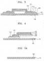
- FIG. 1illustrates a cross-sectional view of a conventional MEMS transducer.
- the conventional transducerincludes a diaphragm layer of silicon nitride, a SiO 2 layer coated by a chemical vapor deposition (CVD) process, a piezo film of zinc oxide (ZnO) and an upper and a lower electrode on a silicon (Si) wafer.
- the CVD process to form a silicon nitride thin film and a silicon oxide layer on a silicon waferis a high temperature process requiring a process temperature of about 780 to 850 °C. Therefore, it is impossible to use a flexible polymeric material other than the silicon wafer as a material for the substrate.
- polymeric materialsare more suitable for use in an electronic system. Polymeric materials, however, have a low melting point in the range of 500 °C or less. Thus, when polymeric materials are subjected to a process for forming a thin film at a high temperature, the polymeric materials deteriorate. Therefore, polymeric materials are not suitable for use as a material for the substrate, such as a wafer, in a process for manufacturing MEMS, which requires a process temperature that is higher than melting points of the polymeric materials.
- silicon MEMS and semiconductorswhich are widely used and have excellent characteristics in terms of performance and degree of integration, are generally produced by methods including a high temperature process of at least 500 °C. Therefore, the substrate of a high molecular (polymeric) material, which is needed for a flexible system structure, cannot be used.
- a conventional MEMS structureis formed by depositing a thin film by chemical vapor deposition (CVD), followed by an etching process.
- CVDchemical vapor deposition
- a very high temperatureis needed to form a high-utility thin film by CVD
- a low-melting point substratesuch as a polymer, glass, or the like, cannot be used.
- a conventional methodproduces a flexible device by forming a sensor device 30 on a silicon substrate 10 using a silicon MEMS process, cutting between silicon islands from a backside of the silicon substrate 10 and then depositing a polymer 11.
- this methodhas disadvantages in that the conventional MEMS process, which includes a high temperature process, is used and a polymer process is additionally performed in a final step, thereby increasing the complexity and the cost of the entire manufacturing process.
- US 5633552discloses cantilever pressure transducers.
- a silicon substrateis etched to provide a thin cantilever structure in an opening of the substrate.
- the transduceris formed directly on the cantilever structure.
- a micromachined moldis used to provide a polymer substrate having a cantilever structure formed in an opening. Again, the transducer is formed directly on the cantilever structure.
- a first aspect of the present inventionprovides a flexible MEMS transducer having the features according to claim 1.
- the transducermay further include a lower protective layer formed by coating either silicon nitride and silicon oxide on the substrate to a thickness of less than about 10 ⁇ m.
- the membrane layeris formed by depositing silicon nitride to a thickness of less than about 5 ⁇ m by PECVD.
- the lower electrode layer and the upper electrode layerare formed of a material selected from the group consisting of metals, such as aluminum, and electrically conductive polymers to a thickness of between about 0.01 ⁇ m to 5 ⁇ m.
- the active layeris formed by depositing a piezopolymer selected from the group consisting of PVDF, PVDF-TrEF, TrEF, Polyurea, polyimid and Nylon to a thickness of between about 1 ⁇ m to 10 ⁇ m and a length of between about 50 ⁇ m to 1000 ⁇ m to have a resonance frequency of between about 1 Hz to 100 kHz.
- a piezopolymerselected from the group consisting of PVDF, PVDF-TrEF, TrEF, Polyurea, polyimid and Nylon to a thickness of between about 1 ⁇ m to 10 ⁇ m and a length of between about 50 ⁇ m to 1000 ⁇ m to have a resonance frequency of between about 1 Hz to 100 kHz.
- the transducermay further include an upper protective layer formed by depositing either silicon nitride or silicon oxide to a thickness of between about 1 ⁇ m to 10 ⁇ m to cover the upper and lower electrode layers and the active layer.
- an upper protective layerformed by depositing either silicon nitride or silicon oxide to a thickness of between about 1 ⁇ m to 10 ⁇ m to cover the upper and lower electrode layers and the active layer.
- the first connecting pad and the second connecting padare formed of a material selected from the group consisting of metals and electrically conductive polymers.
- Another aspect of the present inventionprovides a method for manufacturing a flexible transducer having the steps according to claim 20.
- polyimideis coated to a thickness of less than about 0 to 10 ⁇ m on the substrate and patterned by either wet etching or dry etching in accordance with a desired configuration of the membrane layer.
- silicon nitrideis deposited on the sacrificial layer by PECVD and patterned by drying etching.
- a piezopolymersuch as PVDF, PVDF-TrEF, TrEF, Polyurea, polyimide, Nylon and the like is deposited to a thickness of less than about 10 ⁇ m on the lower electrode layer by spincoating or evaporation and patterned by either wet etching or dry etching.
- the methodmay further include a step to form an upper protective layer to cover the upper and lower electrode layers and the active layer, in which the upper protective layer is formed by depositing either silicon nitride or silicon oxide to a thickness of less than about 10 ⁇ m by PECVD and patterning the deposited layer by either wet etching or dry etching.
- the first connecting padis formed by patterning the upper protective layer at a portion to be connected to the lower electrode layer by either wet etching or dry etching; depositing a metal layer or an electrically conductive polymer layer thereon; and patterning the deposited layer by either wet etching or dry etching.
- the second connecting padis formed by patterning the upper protective layer at a portion to be connected to the upper electrode layer by either wet etching or dry etching; depositing a metal layer or an electrically conductive polymer layer thereon; and patterning the deposited layer by either wet etching or dry etching.
- the present inventionalso provides a flexible wireless MEMS microphone comprising the flexible M EMS transducer structure described above.
- the present inventionthus provides a microphone, which has characteristics of softness, flexibility and foldability, by forming a MEMS transducer structure on a flexible polymer substrate using a plasma enhanced chemical vapor deposition (PECVD) process.
- PECVDplasma enhanced chemical vapor deposition
- FIG. 3illustrates a cross-sectional view of a diaphragm-type transducer according to an embodiment of the present invention.
- FIG. 4illustrates a cross-sectional view of a cantilever-type transducer according to an embodiment of the present invention. As shown in FIGS.
- a transducerincludes a flexible substrate 100, on which a lower protective layer 110 has been formed by depositing either silicon nitride or silicon oxide by plasma enhanced chemical vapor deposition (PECVD) or by sputtering, and a transducer structure including a membrane layer 220 formed by PECVD, which is performed at a low temperature, a lower electrode layer 230, an active layer 240, which is preferably a piezopolymer layer, an upper electrode layer 250 and connecting pads 271 and 272.
- PECVDplasma enhanced chemical vapor deposition
- a sacrificial layeris formed on the substrate 100, the membrane layer 220 is formed thereon, and then the sacrificial layer is removed by an etchant in order to form a raised part of the membrane layer 220. More specifically, in the case of a cantilever-type transducer, the removal of the sacrificial layer under the membrane layer is performed by removing the sacrificial layer through an open side, and in the case of a diaphragm-type transducer, the removal is performed by forming predetermined through holes on the membrane layer 220 by etching and injecting an etchant through the through holes.
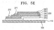
- FIGS. 5A to 5Esequentially illustrate stages in an embodiment of a process for manufacturing the cantilever-type flexible transducer according to the present invention.
- the exemplary transducer shown in the figuresis a cantilever-type, and an exemplary process for manufacturing a cantilever-type transducer will now be explained with reference to FIGS. 5A to 5E.
- the manufacturing process of the flexible transducerstarts with coating a lower protective layer 110 on a flexible substrate 100.
- a flexible materialis used as a material for the flexible substrate 100.
- This flexible materialmay include a high-molecular (polymeric) material, such as polyimide or a metallic thin film.
- a high-molecular materialis the preferred material for use in an electronic system, such as a microphone.
- the lower protective layer 110is formed by coating silicon nitride or silicon oxide by PECVD or sputtering.
- the lower protective layer 110has a thickness of less than about 10 ⁇ m.
- the lower protective layer 110functions to protect the substrate 100 and to facilitate the adhesion of layers, which will be subsequently deposited.
- a sacrificial layer 210is deposited which will be used to form a membrane layer having a raised part of a predetermined length.
- the sacrificial layer 210is formed by coating a polyimide to a thickness of less than about 10 ⁇ m and then patterning the polyimide in accordance with a desired configuration of the membrane layer.
- a membrane layer 220is then deposited on the patterned sacrificial layer 210.
- the membrane layer 220is formed by coating silicon nitride by PECVD in a low temperature process.
- the membrane layer 220has a thickness of less than about 5 ⁇ m.
- a lower electrode 230is deposited on the membrane layer 220.
- the lower electrode layer 230is formed by depositing a metal, such as aluminum or an electrically conductive polymer, and then patterning the deposited layer by either wet etching or dry etching.
- An active layer 240is then coated on the lower electrode layer 230 and the membrane layer 220.
- the active layer 240is formed by coating a piezopolymer, such as PVDF, PVDF-TrEF, TrEF, Polyurea, polyimide, Nylon or the like, by spin coating or evaporation.
- the active layer 240has a thickness of between about 1 ⁇ m to 10 ⁇ m and a length of between about 50 ⁇ m to 1000 ⁇ m.
- the active layer 240has a resonance frequency of between about 1 Hz to 100 kHz.
- an upper electrode 250is then deposited on the piezopolymer active layer 240.
- the upper electrode layer 250is formed by depositing a metal, such as aluminum or an electrically conductive polymer, and patterning the deposited layer by either wet etching or dry etching.
- a metalsuch as aluminum or an electrically conductive polymer
- each of the lower electrode layer 230 and the upper electrode layer 250has a thickness of between about 0.01 ⁇ m to 5 ⁇ m.
- the piezopolymer layeris also patterned by either wet etching or dry etching to form the active layer 240.
- an upper protective layer 260is formed by depositing silicon nitride or silicon oxide to a thickness of between about 1 ⁇ m to 10 ⁇ m by PECVD to cover the upper and lower electrode layers 230 and 250 and the active layer 240 so that the piezopolymer active layer 240 is protected during the removal of the sacrificial layer 210 by etching.
- connecting pads 271, 272are formed to be electrically connected to the upper electrode layer 250 and the lower electrode layer 230, respectively.
- the connecting pads 271 and 272are formed by patterning the upper protective layer 260 at portions to be connected to the upper and lower electrode layers 250 and 230, respectively and by coating a metal, such as aluminum or an electrically conductive polymer, thereon, and then patterning.
- the sacrificial layer 210is removed by dry etching and the formation of the flexible cantilever-type MEMS transducer is completed.
- FIGS. 6A to 6Jillustrate sectional views of stages in a process for manufacturing a cantilever-type transducer according to another embodiment of the present invention.
- a lower protective layer 110is formed by depositing a silicon nitride or silicon oxide on a flexible substrate 100 by plasma enhanced chemical vapor deposition (PECVD) or by sputtering.
- PECVDplasma enhanced chemical vapor deposition
- a sacrificial layer 210is formed by depositing a polyimide to a thickness of less than about 10 ⁇ m and then patterning the polyimide.
- a membrane layer 220, a lower electrode layer 230, an active layer 240 and an upper electrode layer 250are sequentially deposited on the sacrificial layer 210 by PECVD.
- the upper electrode layer 250 and the active layer 240are patterned, and as shown in FIG. 6E, the lower electrode layer 230 is patterned.
- an upper protective layer 260is deposited to cover the upper electrode layer 250, the lower electrode layer 230 and the active layer 240.
- the upper protective layer 260is patterned for an electrical connection of the lower electrode layer 230 and also of the upper electrode layer 250.
- a metal layer or an electrically conductive layeris deposited on the patterned upper protective layer 260, and patterned to form a first connecting pad 272 for connecting with the lower electrode layer 230 and a second connecting pad 271 for connecting with the connecting part of the upper electrode layer 250.
- the membrane layer 220is patterned to expose the sacrificial layer 210, and an etchant is injected to remove the sacrificial layer 210. As a result, a flexible MEMS transducer is completed.
- the layers of the flexible MEMS transducer structuremay be deposited and patterned respectively, or as shown in FIGS. 6A to 6J, the layers may be deposited first and then patterned, respectively.
- the transducer structure 200is formed on a flexible substrate 100, such as a polymer, by using a low-temperature process, such as PECVD.
- a low-temperature processsuch as PECVD.
- the deposition of thin layersis performed by using PECVD or sputtering instead of CVD, which requires a high temperature process of about 780 °C to 850 °C.
- the reason for this difference in required temperature levelsis related to the energy source used in the respective processes.
- the PECVD processuses plasma as an energy source needed for reaction, whereas the conventional CVD process uses heat energy. Therefore, the heat energy can be reduced and thin layers can be formed at a low temperature in PECVD. More particularly, it is possible to deposit thin layers constituting the transducer structure 200 at a low temperature and thereby permitting use a flexible polymeric substrate 100. Consequently, according to the present invention, a flexible microphone of soft material can be manufactured.
- FIG. 7illustrates a schematic view of a skin-type flexible wireless MEMS microphone incorporating the cantilever-type transducer shown in FIG. 4.
- the flexible microphone using the flexible MEMS transduceris prepared by forming an MEMS transducer structure 200 by PECVD on a flexible substrate, as described above, printing a film antenna 300 at a side of the substrate 100 for communicating with an outside source and embedding a wire and interface circuit 400 to electrically connect the film antenna 300 and the flexible MEMS transducer 200.
- the resulting substrate 100is laminated together with a battery layer 500 electrically connected to the flexible substrate 100 for supplying power to the MEMS transducer 200 and a flexible bluetooth module layer 600.
- the battery layer 500is a polymer batter, such as a flexible polymer solar cell and has a paper-like thinness.
- the flexible MEMS microphone prepared by laminating the substrate 100 having the transducer 200 formed with the battery layer 500 and the flexible bluetooth module layer 600 to a predetermined thicknesscan be used as a skin-type flexible MEMS microphone.
- a skin-type flexible MEMS microphoneis freely flexible in all directions and can be used in a wearable device.
- the flexible wireless microphone according to the present inventioncan be packaged into a three-dimensional shape since the flexible substrate 100 can be folded at a predetermined angle.
- the predetermined angleis in the range of less than about 180°.
- FIG. 8illustrates a schematic view of an example of a packaged flexible wireless microphone.
- a flexible MEMS transducer structure 200is formed on a flexible substrate 100.
- An antenna 300is printed on the flexible substrate 100 and a wire and interface circuit 400 is embedded in the flexible substrate 100.
- the flexible substrate 100is then cut in accordance with a development figure of a desired three-dimensional shape of a microphone packaging, folded at a predetermined angle and assembled into the desired three-dimensional shape to form a three-dimensional microphone.
- the substrate 100 on which the flexible MEMS transducer is formedhas paper-like features, it can be cut and folded in accordance with a desired three-dimensional structure of the microphone to be packaged and assembled into the desired three-dimensional structure for packaging.
- the skin-type microphone including the battery layer 500 and the bluetooth module layer 600 laminated on the substrate 100, as shown in FIG. 7,can be cut and folded altogether and assembled into a three-dimensional structure to form a three-dimensional wireless MEMS microphone.
- the flexible battery layer 500 and the flexible bluetooth module layer 600are assembled into a three-dimensional structure.
- the substrate provided with the transducer structure 200, antenna 300 and wire and interface circuit 400 thereonis cut in accordance with a development figure of a desired three-dimensional shape, folded at a predetermined angle and assembled with the three-dimensional structure of the flexible battery layer 500 and the bluetooth module layer 600 to form a three-dimensional MEMS microphone.
- the flexible MEMS wireless microphoneis able to be folded at a predetermined angle, preferably in the range of less than about 180°.
- a microphone structure according to an embodiment of the present inventionis flexible and foldable due to the use of a flexible polymeric substrate. Accordingly, it is possible to package the microphone into a desired three-dimensional structure by cutting and folding the substrate laminated with other elements in accordance with the desired three-dimensional structure and assembling it into a three-dimensional microphone.
- a transducer structurecan, be prepared by a low-temperature process, a flexible polymer substrate can be used.
- a flexible microphone systemhaving excellent characteristics in terms of degree of integration, mobility, softness, flexibility, foldability and wearability by a simple process at a low temperature and at a reduced cost.
- a skin-type microphonewith a desired thickness that can be attached to the body and a three-dimensional microphone due to the flexibility and foldability thereof. Accordingly, various shapes of a packaging structure can be freely designed. Further, the microphone thus-obtained is easy to wear and free to change a shape thereof as needed.
- the flexible microphone according to an embodiment of the present inventioncan be freely prepared in various shapes suitable for application, it can be used as a skin-type microphone and also applied in a flexible MEMS transducer which can be packaged in a desired shape and a method for manufacturing such a flexible MEMS transducer.
Landscapes
- Engineering & Computer Science (AREA)
- Manufacturing & Machinery (AREA)
- Microelectronics & Electronic Packaging (AREA)
- Physics & Mathematics (AREA)
- Acoustics & Sound (AREA)
- Signal Processing (AREA)
- Micromachines (AREA)
- Piezo-Electric Transducers For Audible Bands (AREA)
- Pressure Sensors (AREA)
- Details Of Aerials (AREA)
- Piezo-Electric Or Mechanical Vibrators, Or Delay Or Filter Circuits (AREA)
Description
- The present invention relates to a micro-electromechanical system (MEMS) structure and a method for manufacturing the same. More particularly, the present invention relates to a flexible MEMS transducer formed on a flexible substrate, a manufacturing method thereof, and a flexible MEMS wireless microphone incorporating the flexible MEMS transducer.
- In accordance with the need for very small devices, semiconductor processing technology using micromachining techniques is employed to integrate micro devices. The field of micro-electromechanical systems (MEMS) is a field of manufacturing and testing miniature sensors or actuators, which have sizes on the order of micrometers (µm), and electromechanical structures using micromachining technology applied in semiconductor processing, particularly, in integrated circuit technology.
- The micromachining technology employed in MEMS is largely divided into two categories. The first micromachining category is bulk micromachining by silicon bulk etching. The second micromachining category is surface micromachining by depositing a film of polycrystalline silicon, silicon nitride and silicon oxide on silicon and etching the deposited film according to a predetermined pattern to form a structure. For example, the formation of an ultra small microphone manufactured using a MEMS process is achieved using a diaphragm transducer formed by the bulk micromachining technology.
- FIG. 1 illustrates a cross-sectional view of a conventional MEMS transducer. As shown, the conventional transducer includes a diaphragm layer of silicon nitride, a SiO2 layer coated by a chemical vapor deposition (CVD) process, a piezo film of zinc oxide (ZnO) and an upper and a lower electrode on a silicon (Si) wafer. The CVD process to form a silicon nitride thin film and a silicon oxide layer on a silicon wafer is a high temperature process requiring a process temperature of about 780 to 850 °C. Therefore, it is impossible to use a flexible polymeric material other than the silicon wafer as a material for the substrate.
- Meanwhile, as the information and communication industry develops, demand for a hand-held or wearable information terminal is similarly increasing. This increase in demand is due in part to the applications of such information terminals being implemented into diverse fields, such as medical, service, entertainment, military, and information communication. For convenience in using these information terminals, the components of these terminals should have excellent characteristics in terms of mobility and wearability. In particular, in order to realize a wearable system, a flexible system structure is essential. Therefore, a technology to integrate a functional structure and other electric parts together on a flexible substrate is needed.
- As a flexible substrate, metallic thin films or polymeric materials are used. Polymeric materials are more suitable for use in an electronic system. Polymeric materials, however, have a low melting point in the range of 500 °C or less. Thus, when polymeric materials are subjected to a process for forming a thin film at a high temperature, the polymeric materials deteriorate. Therefore, polymeric materials are not suitable for use as a material for the substrate, such as a wafer, in a process for manufacturing MEMS, which requires a process temperature that is higher than melting points of the polymeric materials. In practice, silicon MEMS and semiconductors, which are widely used and have excellent characteristics in terms of performance and degree of integration, are generally produced by methods including a high temperature process of at least 500 °C. Therefore, the substrate of a high molecular (polymeric) material, which is needed for a flexible system structure, cannot be used.
- Specifically, a conventional MEMS structure is formed by depositing a thin film by chemical vapor deposition (CVD), followed by an etching process. However, since a very high temperature is needed to form a high-utility thin film by CVD, a low-melting point substrate, such as a polymer, glass, or the like, cannot be used.
- In order to overcome such problems, a conventional method, as shown in FIG. 2, produces a flexible device by forming a
sensor device 30 on asilicon substrate 10 using a silicon MEMS process, cutting between silicon islands from a backside of thesilicon substrate 10 and then depositing apolymer 11. However, this method has disadvantages in that the conventional MEMS process, which includes a high temperature process, is used and a polymer process is additionally performed in a final step, thereby increasing the complexity and the cost of the entire manufacturing process. - US 5633552 discloses cantilever pressure transducers. In one version, a silicon substrate is etched to provide a thin cantilever structure in an opening of the substrate. The transducer is formed directly on the cantilever structure. In another version, a micromachined mold is used to provide a polymer substrate having a cantilever structure formed in an opening. Again, the transducer is formed directly on the cantilever structure.
- A first aspect of the present invention provides a flexible MEMS transducer having the features according to claim 1.
- Preferably, the transducer may further include a lower protective layer formed by coating either silicon nitride and silicon oxide on the substrate to a thickness of less than about 10 µm.
- Preferably, the membrane layer is formed by depositing silicon nitride to a thickness of less than about 5 µm by PECVD.
- Preferably, the lower electrode layer and the upper electrode layer are formed of a material selected from the group consisting of metals, such as aluminum, and electrically conductive polymers to a thickness of between about 0.01 µm to 5 µm.
- Preferably, the active layer is formed by depositing a piezopolymer selected from the group consisting of PVDF, PVDF-TrEF, TrEF, Polyurea, polyimid and Nylon to a thickness of between about 1 µm to 10 µm and a length of between about 50 µm to 1000 µm to have a resonance frequency of between about 1 Hz to 100 kHz.
- Preferably, the transducer may further include an upper protective layer formed by depositing either silicon nitride or silicon oxide to a thickness of between about 1 µm to 10 µm to cover the upper and lower electrode layers and the active layer.
- Preferably, the first connecting pad and the second connecting pad are formed of a material selected from the group consisting of metals and electrically conductive polymers.
- Another aspect of the present invention provides a method for manufacturing a flexible transducer having the steps according to claim 20.
- Preferably, to form the sacrificial layer, polyimide is coated to a thickness of less than about 0 to 10 µm on the substrate and patterned by either wet etching or dry etching in accordance with a desired configuration of the membrane layer.
- Preferably, to form the membrane layer, silicon nitride is deposited on the sacrificial layer by PECVD and patterned by drying etching.
- Preferably, to form the active layer, a piezopolymer such as PVDF, PVDF-TrEF, TrEF, Polyurea, polyimide, Nylon and the like is deposited to a thickness of less than about 10 µm on the lower electrode layer by spincoating or evaporation and patterned by either wet etching or dry etching.
- Preferably, the method may further include a step to form an upper protective layer to cover the upper and lower electrode layers and the active layer, in which the upper protective layer is formed by depositing either silicon nitride or silicon oxide to a thickness of less than about 10 µm by PECVD and patterning the deposited layer by either wet etching or dry etching.
- Preferably, the first connecting pad is formed by patterning the upper protective layer at a portion to be connected to the lower electrode layer by either wet etching or dry etching; depositing a metal layer or an electrically conductive polymer layer thereon; and patterning the deposited layer by either wet etching or dry etching. Preferably, the second connecting pad is formed by patterning the upper protective layer at a portion to be connected to the upper electrode layer by either wet etching or dry etching; depositing a metal layer or an electrically conductive polymer layer thereon; and patterning the deposited layer by either wet etching or dry etching.
- The present invention also provides a flexible wireless MEMS microphone comprising the flexible M EMS transducer structure described above.
- The present invention thus provides a microphone, which has characteristics of softness, flexibility and foldability, by forming a MEMS transducer structure on a flexible polymer substrate using a plasma enhanced chemical vapor deposition (PECVD) process.
- The above and other features and advantages of the present invention will become more apparent by describing in detail preferred embodiments thereof with reference to the attached drawings, in which:
- FIG. 1 illustrates a cross-sectional view of a conventional MEMS transducer;
- FIG. 2 illustrates a cross-sectional view of a conventional flexible MEMS sensor;
- FIG. 3 illustrates a cross-sectional view of a diaphragm-type transducer according to an embodiment of the present invention;
- FIG. 4 illustrates a cross-sectional view of a cantilever-type transducer according to an embodiment of the present invention;
- FIGS. 5A to 5E illustrate cross-sectional views of stages in a process for manufacturing the cantilever-type transducer shown in FIG. 4;
- FIGS. 6A to 6J illustrate sectional views of stages in a process for manufacturing a cantilever-type transducer according to another embodiment of the present invention;
- FIG. 7 illustrates a schematic view of a skin-type flexible wireless MEMS microphone incorporating the cantilever-type transducer shown in FIG. 4; and
- FIG. 8 illustrates a schematic view of a three-dimensional wireless microphone packaging incorporating the cantilever-type transducer shown in FIG. 4.
- The present invention will now be described more fully hereinafter with reference to the accompanying drawings, in which preferred embodiments of the invention are shown. The invention may, however, be embodied in different forms and should not be construed as limited to the embodiments set forth herein. Rather, these embodiments are provided so that this disclosure will be thorough and complete, and will fully convey the scope of the invention to those skilled in the art. In the drawings, the thickness of layers and regions are exaggerated for clarity. It will also be understood that when a layer is referred to as being "on" another layer or substrate, it can be directly on the other layer or substrate, or intervening layers may also be present. Like numbers refer to like elements throughout.
- FIG. 3 illustrates a cross-sectional view of a diaphragm-type transducer according to an embodiment of the present invention. FIG. 4 illustrates a cross-sectional view of a cantilever-type transducer according to an embodiment of the present invention. As shown in FIGS. 3 and 4, a transducer according to an embodiment of the present invention includes a
flexible substrate 100, on which a lowerprotective layer 110 has been formed by depositing either silicon nitride or silicon oxide by plasma enhanced chemical vapor deposition (PECVD) or by sputtering, and a transducer structure including amembrane layer 220 formed by PECVD, which is performed at a low temperature, alower electrode layer 230, anactive layer 240, which is preferably a piezopolymer layer, anupper electrode layer 250 and connectingpads substrate 100, themembrane layer 220 is formed thereon, and then the sacrificial layer is removed by an etchant in order to form a raised part of themembrane layer 220. More specifically, in the case of a cantilever-type transducer, the removal of the sacrificial layer under the membrane layer is performed by removing the sacrificial layer through an open side, and in the case of a diaphragm-type transducer, the removal is performed by forming predetermined through holes on themembrane layer 220 by etching and injecting an etchant through the through holes. - FIGS. 5A to 5E sequentially illustrate stages in an embodiment of a process for manufacturing the cantilever-type flexible transducer according to the present invention. The exemplary transducer shown in the figures is a cantilever-type, and an exemplary process for manufacturing a cantilever-type transducer will now be explained with reference to FIGS. 5A to 5E.
- As shown in FIG. 5A, the manufacturing process of the flexible transducer starts with coating a lower
protective layer 110 on aflexible substrate 100. As a material for theflexible substrate 100, a flexible material is used. This flexible material may include a high-molecular (polymeric) material, such as polyimide or a metallic thin film. A high-molecular material is the preferred material for use in an electronic system, such as a microphone. The lowerprotective layer 110 is formed by coating silicon nitride or silicon oxide by PECVD or sputtering. Preferably, the lowerprotective layer 110 has a thickness of less than about 10 µm. By using the PECVD or sputtering process, it is possible to perform the process at a low-temperature process of about 400 °C or less. The lowerprotective layer 110 functions to protect thesubstrate 100 and to facilitate the adhesion of layers, which will be subsequently deposited. - As shown in FIG. 5B, on the
flexible substrate 100 on which the lowerprotective layer 110 is coated, asacrificial layer 210 is deposited which will be used to form a membrane layer having a raised part of a predetermined length. Thesacrificial layer 210 is formed by coating a polyimide to a thickness of less than about 10 µm and then patterning the polyimide in accordance with a desired configuration of the membrane layer. Amembrane layer 220 is then deposited on the patternedsacrificial layer 210. Themembrane layer 220 is formed by coating silicon nitride by PECVD in a low temperature process. Preferably, themembrane layer 220 has a thickness of less than about 5 µm. Next, alower electrode 230 is deposited on themembrane layer 220. Thelower electrode layer 230 is formed by depositing a metal, such as aluminum or an electrically conductive polymer, and then patterning the deposited layer by either wet etching or dry etching. Anactive layer 240 is then coated on thelower electrode layer 230 and themembrane layer 220. Theactive layer 240 is formed by coating a piezopolymer, such as PVDF, PVDF-TrEF, TrEF, Polyurea, polyimide, Nylon or the like, by spin coating or evaporation. Preferably, theactive layer 240 has a thickness of between about 1 µm to 10 µm and a length of between about 50 µm to 1000 µm. Preferably, theactive layer 240 has a resonance frequency of between about 1 Hz to 100 kHz. - As shown in FIG. 5C, an
upper electrode 250 is then deposited on the piezopolymeractive layer 240. Theupper electrode layer 250 is formed by depositing a metal, such as aluminum or an electrically conductive polymer, and patterning the deposited layer by either wet etching or dry etching. Preferably, each of thelower electrode layer 230 and theupper electrode layer 250 has a thickness of between about 0.01 µm to 5 µm. At this time, the piezopolymer layer is also patterned by either wet etching or dry etching to form theactive layer 240. - Next, as shown in FIG. 5D, an upper
protective layer 260 is formed by depositing silicon nitride or silicon oxide to a thickness of between about 1 µm to 10 µm by PECVD to cover the upper andlower electrode layers active layer 240 so that the piezopolymeractive layer 240 is protected during the removal of thesacrificial layer 210 by etching. After forming the upperprotective layer 260, connectingpads upper electrode layer 250 and thelower electrode layer 230, respectively. The connectingpads protective layer 260 at portions to be connected to the upper andlower electrode layers - Finally, as shown in FIG. 5E, the
sacrificial layer 210 is removed by dry etching and the formation of the flexible cantilever-type MEMS transducer is completed. - FIGS. 6A to 6J illustrate sectional views of stages in a process for manufacturing a cantilever-type transducer according to another embodiment of the present invention.
- As shown in FIG. 6A, a lower
protective layer 110 is formed by depositing a silicon nitride or silicon oxide on aflexible substrate 100 by plasma enhanced chemical vapor deposition (PECVD) or by sputtering. Next, as shown in FIG. 6B, asacrificial layer 210 is formed by depositing a polyimide to a thickness of less than about 10 µm and then patterning the polyimide. - After the
sacrificial layer 210 is formed, as shown in FIG. 6C, amembrane layer 220, alower electrode layer 230, anactive layer 240 and anupper electrode layer 250 are sequentially deposited on thesacrificial layer 210 by PECVD. Next, as shown in FIG. 6D, theupper electrode layer 250 and theactive layer 240 are patterned, and as shown in FIG. 6E, thelower electrode layer 230 is patterned. - Subsequently, as shown in FIG. 6F, an upper
protective layer 260 is deposited to cover theupper electrode layer 250, thelower electrode layer 230 and theactive layer 240. After the deposition of the upperprotective layer 260, as shown in FIG. 6G, the upperprotective layer 260 is patterned for an electrical connection of thelower electrode layer 230 and also of theupper electrode layer 250. A metal layer or an electrically conductive layer is deposited on the patterned upperprotective layer 260, and patterned to form a first connectingpad 272 for connecting with thelower electrode layer 230 and a second connectingpad 271 for connecting with the connecting part of theupper electrode layer 250. Next, as shown in FIG. 61, themembrane layer 220 is patterned to expose thesacrificial layer 210, and an etchant is injected to remove thesacrificial layer 210. As a result, a flexible MEMS transducer is completed. - As for the method for manufacturing the flexible MEMS transducers, as shown in FIGS. 5A to 5E, the layers of the flexible MEMS transducer structure may be deposited and patterned respectively, or as shown in FIGS. 6A to 6J, the layers may be deposited first and then patterned, respectively.
- According to the above-described manufacturing method, it is possible to form a
transducer structure 200 on aflexible substrate 100, such as a polymer, by using a low-temperature process, such as PECVD. Thus, in thetransducer structure 200 according to an embodiment of the present invention, the deposition of thin layers is performed by using PECVD or sputtering instead of CVD, which requires a high temperature process of about 780 °C to 850 °C. The reason for this difference in required temperature levels is related to the energy source used in the respective processes. Specifically, the PECVD process uses plasma as an energy source needed for reaction, whereas the conventional CVD process uses heat energy. Therefore, the heat energy can be reduced and thin layers can be formed at a low temperature in PECVD. More particularly, it is possible to deposit thin layers constituting thetransducer structure 200 at a low temperature and thereby permitting use a flexiblepolymeric substrate 100. Consequently, according to the present invention, a flexible microphone of soft material can be manufactured. - Application of the present invention further provides a freely flexible microphone incorporating a flexible MEMS transducer according to an embodiment of the present invention. FIG. 7 illustrates a schematic view of a skin-type flexible wireless MEMS microphone incorporating the cantilever-type transducer shown in FIG. 4. As shown in FIG. 7, the flexible microphone using the flexible MEMS transducer is prepared by forming an
MEMS transducer structure 200 by PECVD on a flexible substrate, as described above, printing afilm antenna 300 at a side of thesubstrate 100 for communicating with an outside source and embedding a wire andinterface circuit 400 to electrically connect thefilm antenna 300 and theflexible MEMS transducer 200. The resultingsubstrate 100 is laminated together with abattery layer 500 electrically connected to theflexible substrate 100 for supplying power to theMEMS transducer 200 and a flexiblebluetooth module layer 600. Preferably, thebattery layer 500 is a polymer batter, such as a flexible polymer solar cell and has a paper-like thinness. - Thus, the flexible MEMS microphone prepared by laminating the
substrate 100 having thetransducer 200 formed with thebattery layer 500 and the flexiblebluetooth module layer 600 to a predetermined thickness can be used as a skin-type flexible MEMS microphone. Such a skin-type flexible MEMS microphone is freely flexible in all directions and can be used in a wearable device. - In addition, the flexible wireless microphone according to the present invention can be packaged into a three-dimensional shape since the
flexible substrate 100 can be folded at a predetermined angle. Preferably, the predetermined angle is in the range of less than about 180°. FIG. 8 illustrates a schematic view of an example of a packaged flexible wireless microphone. As shown in FIG. 8, a flexibleMEMS transducer structure 200 is formed on aflexible substrate 100. Anantenna 300 is printed on theflexible substrate 100 and a wire andinterface circuit 400 is embedded in theflexible substrate 100. Theflexible substrate 100 is then cut in accordance with a development figure of a desired three-dimensional shape of a microphone packaging, folded at a predetermined angle and assembled into the desired three-dimensional shape to form a three-dimensional microphone. - Since the
substrate 100 on which the flexible MEMS transducer is formed has paper-like features, it can be cut and folded in accordance with a desired three-dimensional structure of the microphone to be packaged and assembled into the desired three-dimensional structure for packaging. - The skin-type microphone including the
battery layer 500 and thebluetooth module layer 600 laminated on thesubstrate 100, as shown in FIG. 7, can be cut and folded altogether and assembled into a three-dimensional structure to form a three-dimensional wireless MEMS microphone. Alternatively, as shown in FIG. 8, theflexible battery layer 500 and the flexiblebluetooth module layer 600 are assembled into a three-dimensional structure. Separately, the substrate provided with thetransducer structure 200,antenna 300 and wire andinterface circuit 400 thereon is cut in accordance with a development figure of a desired three-dimensional shape, folded at a predetermined angle and assembled with the three-dimensional structure of theflexible battery layer 500 and thebluetooth module layer 600 to form a three-dimensional MEMS microphone. The flexible MEMS wireless microphone is able to be folded at a predetermined angle, preferably in the range of less than about 180°. - More particularly, a microphone structure according to an embodiment of the present invention is flexible and foldable due to the use of a flexible polymeric substrate. Accordingly, it is possible to package the microphone into a desired three-dimensional structure by cutting and folding the substrate laminated with other elements in accordance with the desired three-dimensional structure and assembling it into a three-dimensional microphone.
- As described above, according to the present invention, since a transducer structure can, be prepared by a low-temperature process, a flexible polymer substrate can be used. Thus, it is possible to produce a flexible microphone system having excellent characteristics in terms of degree of integration, mobility, softness, flexibility, foldability and wearability by a simple process at a low temperature and at a reduced cost. Moreover, it is possible to package a skin-type microphone with a desired thickness that can be attached to the body and a three-dimensional microphone due to the flexibility and foldability thereof. Accordingly, various shapes of a packaging structure can be freely designed. Further, the microphone thus-obtained is easy to wear and free to change a shape thereof as needed.
- In addition, since the flexible microphone according to an embodiment of the present invention can be freely prepared in various shapes suitable for application, it can be used as a skin-type microphone and also applied in a flexible MEMS transducer which can be packaged in a desired shape and a method for manufacturing such a flexible MEMS transducer.
- Preferred embodiments of the present invention have been disclosed herein and, although specific terms are employed, they are used and are to be interpreted in a generic and descriptive sense only and not for purpose of limitation. Accordingly, it will be understood by those of ordinary skill in the art that various changes in form and details may be made without departing from the scope of the present invention as set forth in the following claims.
Claims (41)
- A flexible MEMS transducer comprising:a substrate (100), formed of a flexible polymeric or metallic thin film material;a membrane layer (220) provided on the substrate (100), the membrane layer (220) having a raised part of a predetermined length which is separated from the substrate (100);a lower electrode layer (230), formed of an electrically conductive material, provided on the membrane layer (220);an active layer (240), formed of a piezopolymer, provided on the lower electrode layer (230);an upper electrode layer (250), formed of an electrically conductive material, provided on the active layer (240);a first connecting pad (272) electrically connected to the lower electrode layer (230); anda second connecting pad (271) electrically connected to the upper electrode layer (250).
- The flexible MEMS transducer as claimed in claim 1, further comprising a lower protective layer (110) coated on the substrate.
- The flexible MEMS transducer as claimed in claim 2, the lower protective layer (110) is formed of either silicon nitride or silicon oxide.
- The flexible MEMS transducer as claimed in claim 2 or 3, wherein the lower protective layer (110) has a thickness of less than 10 µm.
- The flexible MEMS transducer as claimed in any one of the preceding claims, wherein the substrate (100) is formed of polyimide.
- The flexible MEMS transducer as claimed in any one of the preceding claims, wherein the membrane layer (220) is formed of silicon nitride.
- The flexible MEMS transducer as claimed in any one of the preceding claims, wherein the membrane layer (220) has a thickness of less than 5 µm.
- The flexible MEMS transducer as claimed in any one of the preceding claims, wherein the lower electrode layer (230) and the upper electrode layer (250) are formed of a material selected from the group consisting of metals and electrically conductive polymers.
- The flexible MEMS transducer as claimed in claim 8, wherein the material of the lower electrode layer (230) and the upper electrode layer (250) is aluminum.
- The flexible MEMS transducer as claimed in any one of the preceding claims, wherein the lower electrode layer (230) has a thickness of between 0.01 µm to 5 µm.
- The flexible MEMS transducer as claimed in any one of the preceding claims, wherein the upper electrode layer (250) has a thickness of between 0.01 µm to 5 µm.
- The flexible MEMS transducer as claimed in any one of the preceding claims, wherein the piezopolymer is selected from the group consisting of PVDF, PVDF-TrEF, TrEF, Polyurea, polyimide and Nylon.
- The flexible MEMS transducer as claimed in any one of the preceding claims, wherein the active layer (240) has a thickness of between 1 µm to 10 µm.
- The flexible MEMS transducer as claimed in any one of the preceding claims, wherein the active layer (240) has a resonance frequency of between 1 Hz to 100 kHz.
- The flexible MEMS transducer as claimed in any one of the preceding claims, wherein the active layer (240) has a length of between 50 µm to 1000 µm.
- The flexible MEMS transducer as claimed in any one of the preceding claims, further comprising an upper protective layer (260) to cover the upper and lower electrode layers (230, 250) and the active layer (240).
- The flexible MEMS transducer as claimed in claim 16, wherein the upper protective layer (260) is formed of either silicon nitride or silicon oxide.
- The flexible MEMS transducer as claimed in claim 16 or 17, wherein the upper protective layer (260) has a thickness of between 1 µm to 10 µm.
- The flexible MEMS transducer as claimed in any one of the preceding claims, wherein the first connecting pad (272) and the second connecting pad (271) are formed of a material selected from the group consisting of metals and electrically conductive polymers.
- A method for manufacturing a flexible MEMS transducer comprising:forming a sacrificial layer (210) on a flexible substrate (100), the substrate (100) being formed of a flexible polymeric or metallic thin film material;depositing a membrane layer (220) on the sacrificial layer (210) by plasma enhanced chemical vapor deposition, hereinafter PECVD;depositing a lower electrode layer (230) on the membrane layer (220);depositing an active layer (240) on the lower electrode layer (230);depositing an upper electrode layer (250) on the active layer (240);forming a first connecting pad (272) to be connected to the lower electrode layer (230) and a second connecting pad (271) to be connected to the upper electrode layer (240); andremoving the sacrificial layer (210).
- The method as claimed in claim 20, further comprising:forming a lower protective layer (110) by depositing either silicon nitride or silicon oxide by PECVD, before depositing the sacrificial layer (210).
- The method as claimed in claim 20 or 21, wherein forming the sacrificial layer is performed by coating a polyimide layer on the substrate and patterning the coated polyimide layer by either wet etching or dry etching in accordance with a desired configuration of the membrane layer.
- The method as claimed in any one of claims 20 to 22, wherein the sacrificial layer (210) is formed to a thickness of less than 10 µm.
- The method as claimed in any one of claims 20 to 23, wherein forming the membrane layer (220) comprises:depositing a silicon nitride layer on the sacrificial layer (210) by PECVD; andpatterning the deposited silicon nitride layer by dry etching.
- The method as claimed in any one of claims 20 to 24, wherein forming the active layer (240) comprises:depositing a piezopolymer layer on the lower electrode layer (230) by either spin coating or evaporation; andpatterning the deposited piezopolymer layer by either wet etching or dry etching.
- The method as claimed in claim 25, wherein the piezopolymer is selected from the group consisting of PVDF, PVDF-TrEF, TrEF, Polyurea, polyimide and Nylon.
- The method as claimed in any one of claims 20 to 26, wherein the active layer (240) is formed to a thickness less than 10 µm.
- The method as claimed in any one of claims 20 to 27, further comprising:forming an upper protective layer (260) to cover the upper and lower electrode layers (230, 250) and the active layer (240), in which the upper protective layer (260) is formed by depositing either silicon nitride or silicon oxide by PECVD and then patterning the deposited layer by either wet etching or dry etching.
- The method as claimed in claim 28, wherein the upper protective layer (260) is formed to a thickness of less than 10 µm.
- The method as claimed in any one of claims 20 to 29, wherein forming the first connecting pad (272) comprises:patterning the upper protective layer (260) at a portion to be connected to the lower electrode layer (230) by either wet etching or dry etching;depositing a metal layer or an electrically conductive polymer layer thereon; andpatterning the deposited layer by either wet etching or dry etching.
- The method as claimed in any one of claims 20 to 30, wherein forming the second connecting pad (271) comprises:patterning the upper protective layer (260) at a portion to be connected to the upper electrode layer (250) by either wet etching or dry etching;depositing a metal layer or an electrically conductive polymer layer thereon; andpatterning the deposited layer by either wet etching or dry etching.
- The method as claimed in claim 20, wherein the sacrificial layer (210), the lower electrode layer (230), the active layer (240), and the upper electrode layer (250) are each patterned.
- The method as claimed in claim 20, wherein the sacrificial layer (210), the lower electrode layer (230), the active layer (240), and the upper electrode layer (250) are deposited on each other and then patterned.
- A flexible wireless MEMS microphone comprising:the flexible MEMS transducer (200), including the substrate (100), as claimed in any of claims 1 to 19;an antenna (300) printed on the substrate (100) for communicating with an outside source;a wire and interface circuit (400) embedded in the substrate (100) to electrically connect the flexible MEMS transducer (200) and the antenna (300);a flexible battery layer (500) electrically connected to the substrate (100); anda bluetooth module layer (600).
- The flexible wireless MEMS microphone as claimed in claim 34, wherein the flexible battery layer (500) is arranged to supply power to the MEMS transducer (200), and wherein the bluetooth module layer (600) is a flexible bluetooth module layer electrically connected to the battery layer (500).
- The flexible wireless MEMS microphone as claimed in claim 34 or 35, wherein the battery layer (500) is a polymer battery having a paper-like thinness.
- The flexible wireless MEMS microphone as claimed in any one of claims 34 to 36, wherein the battery layer (500) is a flexible solar cell.
- The flexible wireless MEMS microphone as claimed in any one of claims 34 to 37, wherein the flexible substrate (100), on which the flexible MEMS transducer is formed, the antenna (300) is printed, and the wire and interface circuit (400) are embedded, is foldable.
- The flexible wireless MEMS microphone as claimed in claim 38, wherein the flexible MEMS wireless microphone is foldable.
- The flexible wireless MEMS microphone as claimed in any one of claims 34 to 39, wherein the flexible wireless MEMS microphone is formable into a desired three-dimensional structure by cutting in accordance with a side shape of the desired three-dimensional structure, folding the cut piece at a predetermined angle, and assembling into the three-dimensional structure.
- The flexible wireless MEMS microphone as claimed in claim 40, wherein the flexible MEMS wireless microphone is formed into the three-dimensional structure.
Applications Claiming Priority (2)
| Application Number | Priority Date | Filing Date | Title |
|---|---|---|---|
| KR2002058313 | 2002-09-26 | ||
| KR10-2002-0058313AKR100512960B1 (en) | 2002-09-26 | 2002-09-26 | Flexible MEMS transducer and its manufacturing method, and flexible MEMS wireless microphone |
Publications (3)
| Publication Number | Publication Date |
|---|---|
| EP1403212A2 EP1403212A2 (en) | 2004-03-31 |
| EP1403212A3 EP1403212A3 (en) | 2005-07-13 |
| EP1403212B1true EP1403212B1 (en) | 2007-02-28 |
Family
ID=36598028
Family Applications (1)
| Application Number | Title | Priority Date | Filing Date |
|---|---|---|---|
| EP03256049AExpired - LifetimeEP1403212B1 (en) | 2002-09-26 | 2003-09-25 | Flexible mems transducer and manufacturing method thereof, and flexible mems wireless microphone |
Country Status (7)
| Country | Link |
|---|---|
| US (1) | US6967362B2 (en) |
| EP (1) | EP1403212B1 (en) |
| JP (1) | JP4126003B2 (en) |
| KR (1) | KR100512960B1 (en) |
| CN (1) | CN100411968C (en) |
| DE (1) | DE60312087T2 (en) |
| TW (1) | TWI235011B (en) |
Cited By (35)
| Publication number | Priority date | Publication date | Assignee | Title |
|---|---|---|---|---|
| US7920319B2 (en) | 2007-07-02 | 2011-04-05 | Qualcomm Mems Technologies, Inc. | Electromechanical device with optical function separated from mechanical and electrical function |
| US7924494B2 (en) | 2004-09-27 | 2011-04-12 | Qualcomm Mems Technologies, Inc. | Apparatus and method for reducing slippage between structures in an interferometric modulator |
| US7936497B2 (en) | 2004-09-27 | 2011-05-03 | Qualcomm Mems Technologies, Inc. | MEMS device having deformable membrane characterized by mechanical persistence |
| US7944604B2 (en) | 2008-03-07 | 2011-05-17 | Qualcomm Mems Technologies, Inc. | Interferometric modulator in transmission mode |
| US7952787B2 (en) | 2006-06-30 | 2011-05-31 | Qualcomm Mems Technologies, Inc. | Method of manufacturing MEMS devices providing air gap control |
| US7982700B2 (en) | 2004-09-27 | 2011-07-19 | Qualcomm Mems Technologies, Inc. | Conductive bus structure for interferometric modulator array |
| US7999993B2 (en) | 2004-09-27 | 2011-08-16 | Qualcomm Mems Technologies, Inc. | Reflective display device having viewable display on both sides |
| US8008736B2 (en) | 2004-09-27 | 2011-08-30 | Qualcomm Mems Technologies, Inc. | Analog interferometric modulator device |
| US8023167B2 (en) | 2008-06-25 | 2011-09-20 | Qualcomm Mems Technologies, Inc. | Backlight displays |
| US8035883B2 (en) | 2004-09-27 | 2011-10-11 | Qualcomm Mems Technologies, Inc. | Device having a conductive light absorbing mask and method for fabricating same |
| US8054527B2 (en) | 2007-10-23 | 2011-11-08 | Qualcomm Mems Technologies, Inc. | Adjustably transmissive MEMS-based devices |
| US8058549B2 (en) | 2007-10-19 | 2011-11-15 | Qualcomm Mems Technologies, Inc. | Photovoltaic devices with integrated color interferometric film stacks |
| US8068269B2 (en) | 2008-03-27 | 2011-11-29 | Qualcomm Mems Technologies, Inc. | Microelectromechanical device with spacing layer |
| US8081373B2 (en) | 2007-07-31 | 2011-12-20 | Qualcomm Mems Technologies, Inc. | Devices and methods for enhancing color shift of interferometric modulators |
| US8081370B2 (en) | 2004-09-27 | 2011-12-20 | Qualcomm Mems Technologies, Inc. | Support structures for electromechanical systems and methods of fabricating the same |
| US8098416B2 (en) | 2006-06-01 | 2012-01-17 | Qualcomm Mems Technologies, Inc. | Analog interferometric modulator device with electrostatic actuation and release |
| US8098417B2 (en) | 2007-05-09 | 2012-01-17 | Qualcomm Mems Technologies, Inc. | Electromechanical system having a dielectric movable membrane |
| US8115987B2 (en) | 2007-02-01 | 2012-02-14 | Qualcomm Mems Technologies, Inc. | Modulating the intensity of light from an interferometric reflector |
| US8130440B2 (en) | 2007-10-19 | 2012-03-06 | Qualcomm Mems Technologies, Inc. | Display with integrated photovoltaic device |
| US8164821B2 (en) | 2008-02-22 | 2012-04-24 | Qualcomm Mems Technologies, Inc. | Microelectromechanical device with thermal expansion balancing layer or stiffening layer |
| US8193441B2 (en) | 2007-12-17 | 2012-06-05 | Qualcomm Mems Technologies, Inc. | Photovoltaics with interferometric ribbon masks |
| US8213075B2 (en) | 2004-09-27 | 2012-07-03 | Qualcomm Mems Technologies, Inc. | Method and device for multistate interferometric light modulation |
| US8270062B2 (en) | 2009-09-17 | 2012-09-18 | Qualcomm Mems Technologies, Inc. | Display device with at least one movable stop element |
| US8270056B2 (en) | 2009-03-23 | 2012-09-18 | Qualcomm Mems Technologies, Inc. | Display device with openings between sub-pixels and method of making same |
| US8289613B2 (en) | 2004-09-27 | 2012-10-16 | Qualcomm Mems Technologies, Inc. | Electromechanical device with optical function separated from mechanical and electrical function |
| US8358266B2 (en) | 2008-09-02 | 2013-01-22 | Qualcomm Mems Technologies, Inc. | Light turning device with prismatic light turning features |
| US8405899B2 (en) | 2004-09-27 | 2013-03-26 | Qualcomm Mems Technologies, Inc | Photonic MEMS and structures |
| US8488228B2 (en) | 2009-09-28 | 2013-07-16 | Qualcomm Mems Technologies, Inc. | Interferometric display with interferometric reflector |
| US8659816B2 (en) | 2011-04-25 | 2014-02-25 | Qualcomm Mems Technologies, Inc. | Mechanical layer and methods of making the same |
| US8797632B2 (en) | 2010-08-17 | 2014-08-05 | Qualcomm Mems Technologies, Inc. | Actuation and calibration of charge neutral electrode of a display device |
| US8817357B2 (en) | 2010-04-09 | 2014-08-26 | Qualcomm Mems Technologies, Inc. | Mechanical layer and methods of forming the same |
| US8941631B2 (en) | 2007-11-16 | 2015-01-27 | Qualcomm Mems Technologies, Inc. | Simultaneous light collection and illumination on an active display |
| US8963159B2 (en) | 2011-04-04 | 2015-02-24 | Qualcomm Mems Technologies, Inc. | Pixel via and methods of forming the same |
| US9057872B2 (en) | 2010-08-31 | 2015-06-16 | Qualcomm Mems Technologies, Inc. | Dielectric enhanced mirror for IMOD display |
| US9134527B2 (en) | 2011-04-04 | 2015-09-15 | Qualcomm Mems Technologies, Inc. | Pixel via and methods of forming the same |
Families Citing this family (144)
| Publication number | Priority date | Publication date | Assignee | Title |
|---|---|---|---|---|
| US7297471B1 (en) | 2003-04-15 | 2007-11-20 | Idc, Llc | Method for manufacturing an array of interferometric modulators |
| US7550794B2 (en) | 2002-09-20 | 2009-06-23 | Idc, Llc | Micromechanical systems device comprising a displaceable electrode and a charge-trapping layer |
| US6794119B2 (en) | 2002-02-12 | 2004-09-21 | Iridigm Display Corporation | Method for fabricating a structure for a microelectromechanical systems (MEMS) device |
| US7781850B2 (en) | 2002-09-20 | 2010-08-24 | Qualcomm Mems Technologies, Inc. | Controlling electromechanical behavior of structures within a microelectromechanical systems device |
| KR100512988B1 (en)* | 2002-09-26 | 2005-09-07 | 삼성전자주식회사 | Manufacturing method for Flexible MEMS transducer |
| TW594360B (en) | 2003-04-21 | 2004-06-21 | Prime View Int Corp Ltd | A method for fabricating an interference display cell |
| US7045246B2 (en)* | 2003-04-22 | 2006-05-16 | The Aerospace Corporation | Integrated thin film battery and circuit module |
| US7434476B2 (en)* | 2003-05-07 | 2008-10-14 | Califronia Institute Of Technology | Metallic thin film piezoresistive transduction in micromechanical and nanomechanical devices and its application in self-sensing SPM probes |
| TW570896B (en) | 2003-05-26 | 2004-01-11 | Prime View Int Co Ltd | A method for fabricating an interference display cell |
| US7221495B2 (en)* | 2003-06-24 | 2007-05-22 | Idc Llc | Thin film precursor stack for MEMS manufacturing |
| TWI231865B (en) | 2003-08-26 | 2005-05-01 | Prime View Int Co Ltd | An interference display cell and fabrication method thereof |
| TW593126B (en) | 2003-09-30 | 2004-06-21 | Prime View Int Co Ltd | A structure of a micro electro mechanical system and manufacturing the same |
| US7012726B1 (en) | 2003-11-03 | 2006-03-14 | Idc, Llc | MEMS devices with unreleased thin film components |
| DE102004030748A1 (en)* | 2004-06-25 | 2006-01-12 | Sennheiser Electronic Gmbh & Co. Kg | Electro-acoustic back electret converter |
| EP2246726B1 (en) | 2004-07-29 | 2013-04-03 | QUALCOMM MEMS Technologies, Inc. | System and method for micro-electromechanical operating of an interferometric modulator |
| US20080004700A1 (en)* | 2004-09-22 | 2008-01-03 | Laxminarayana Saggere | Light Powdered Microactuator, Microfluidic Dispenser and Retinal Prosthesis |
| US7369296B2 (en)* | 2004-09-27 | 2008-05-06 | Idc, Llc | Device and method for modifying actuation voltage thresholds of a deformable membrane in an interferometric modulator |
| US7429334B2 (en) | 2004-09-27 | 2008-09-30 | Idc, Llc | Methods of fabricating interferometric modulators by selectively removing a material |
| US7684104B2 (en) | 2004-09-27 | 2010-03-23 | Idc, Llc | MEMS using filler material and method |
| US7161730B2 (en) | 2004-09-27 | 2007-01-09 | Idc, Llc | System and method for providing thermal compensation for an interferometric modulator display |
| US7349136B2 (en) | 2004-09-27 | 2008-03-25 | Idc, Llc | Method and device for a display having transparent components integrated therein |
| US7327510B2 (en)* | 2004-09-27 | 2008-02-05 | Idc, Llc | Process for modifying offset voltage characteristics of an interferometric modulator |
| US7405861B2 (en) | 2004-09-27 | 2008-07-29 | Idc, Llc | Method and device for protecting interferometric modulators from electrostatic discharge |
| US7373026B2 (en)* | 2004-09-27 | 2008-05-13 | Idc, Llc | MEMS device fabricated on a pre-patterned substrate |
| US7553684B2 (en) | 2004-09-27 | 2009-06-30 | Idc, Llc | Method of fabricating interferometric devices using lift-off processing techniques |
| US7417783B2 (en) | 2004-09-27 | 2008-08-26 | Idc, Llc | Mirror and mirror layer for optical modulator and method |
| US7492502B2 (en) | 2004-09-27 | 2009-02-17 | Idc, Llc | Method of fabricating a free-standing microstructure |
| TW200628877A (en) | 2005-02-04 | 2006-08-16 | Prime View Int Co Ltd | Method of manufacturing optical interference type color display |
| US7642612B2 (en)* | 2005-06-17 | 2010-01-05 | Semiconductor Energy Laboratory Co., Ltd. | Semiconductor device and manufacturing method thereof |
| KR20080041663A (en) | 2005-07-22 | 2008-05-13 | 콸콤 인코포레이티드 | Supporting structures for MEMS devices and methods thereof |
| EP2495212A3 (en)* | 2005-07-22 | 2012-10-31 | QUALCOMM MEMS Technologies, Inc. | Mems devices having support structures and methods of fabricating the same |
| KR101375337B1 (en) | 2005-07-22 | 2014-03-18 | 퀄컴 엠이엠에스 테크놀로지스, 인크. | Electomechanical devices having support structures and methods of fabricating the same |
| WO2007015593A1 (en)* | 2005-08-02 | 2007-02-08 | Bse Co., Ltd | Silicon based condenser microphone and packaging method for the same |
| KR100675027B1 (en)* | 2005-08-10 | 2007-01-30 | 주식회사 비에스이 | Silicon condenser microphone and mounting method for the same |
| KR100644730B1 (en)* | 2005-08-20 | 2006-11-10 | 주식회사 비에스이 | Silicon condenser microphone |
| KR100675025B1 (en)* | 2005-08-20 | 2007-01-29 | 주식회사 비에스이 | Silicon condenser microphone |
| CN101304942B (en)* | 2005-09-09 | 2011-12-07 | Nxp股份有限公司 | MEMS capacitor microphone and manufacturing method, foil stack, electronic device and use |
| US7418281B2 (en) | 2005-09-13 | 2008-08-26 | International Business Machines Corporation | Centralized voice recognition unit for wireless control of personal mobile electronic devices |
| US7362035B2 (en)* | 2005-09-22 | 2008-04-22 | The Penn State Research Foundation | Polymer bulk acoustic resonator |
| EP1928780A2 (en) | 2005-09-30 | 2008-06-11 | Qualcomm Mems Technologies, Inc. | Mems device and interconnects for same |
| KR100670946B1 (en)* | 2005-10-27 | 2007-01-17 | 학교법인 포항공과대학교 | Multiscale cantilever structure having nano-sized microholes and method for manufacturing the same |
| US7630114B2 (en) | 2005-10-28 | 2009-12-08 | Idc, Llc | Diffusion barrier layer for MEMS devices |
| US7808253B2 (en)* | 2005-12-02 | 2010-10-05 | Semiconductor Energy Laboratory Co., Ltd. | Test method of microstructure body and micromachine |
| US7795061B2 (en) | 2005-12-29 | 2010-09-14 | Qualcomm Mems Technologies, Inc. | Method of creating MEMS device cavities by a non-etching process |
| US7916980B2 (en) | 2006-01-13 | 2011-03-29 | Qualcomm Mems Technologies, Inc. | Interconnect structure for MEMS device |
| US7382515B2 (en) | 2006-01-18 | 2008-06-03 | Qualcomm Mems Technologies, Inc. | Silicon-rich silicon nitrides as etch stops in MEMS manufacture |
| US7652814B2 (en) | 2006-01-27 | 2010-01-26 | Qualcomm Mems Technologies, Inc. | MEMS device with integrated optical element |
| US7547568B2 (en) | 2006-02-22 | 2009-06-16 | Qualcomm Mems Technologies, Inc. | Electrical conditioning of MEMS device and insulating layer thereof |
| US7450295B2 (en)* | 2006-03-02 | 2008-11-11 | Qualcomm Mems Technologies, Inc. | Methods for producing MEMS with protective coatings using multi-component sacrificial layers |
| US7443082B2 (en) | 2006-03-03 | 2008-10-28 | Basf Corporation | Piezoelectric polymer composite article and system |
| EP2007671A2 (en)* | 2006-04-10 | 2008-12-31 | Nxp B.V. | Inter-layer connection for foil mems technology |
| US7643203B2 (en) | 2006-04-10 | 2010-01-05 | Qualcomm Mems Technologies, Inc. | Interferometric optical display system with broadband characteristics |
| US7711239B2 (en) | 2006-04-19 | 2010-05-04 | Qualcomm Mems Technologies, Inc. | Microelectromechanical device and method utilizing nanoparticles |
| US7527996B2 (en) | 2006-04-19 | 2009-05-05 | Qualcomm Mems Technologies, Inc. | Non-planar surface structures and process for microelectromechanical systems |
| US7417784B2 (en) | 2006-04-19 | 2008-08-26 | Qualcomm Mems Technologies, Inc. | Microelectromechanical device and method utilizing a porous surface |
| US7623287B2 (en) | 2006-04-19 | 2009-11-24 | Qualcomm Mems Technologies, Inc. | Non-planar surface structures and process for microelectromechanical systems |
| US7369292B2 (en)* | 2006-05-03 | 2008-05-06 | Qualcomm Mems Technologies, Inc. | Electrode and interconnect materials for MEMS devices |
| US20070268209A1 (en)* | 2006-05-16 | 2007-11-22 | Kenneth Wargon | Imaging Panels Including Arrays Of Audio And Video Input And Output Elements |
| US7561277B2 (en)* | 2006-05-19 | 2009-07-14 | New Jersey Institute Of Technology | MEMS fiber optic microphone |
| WO2008100266A2 (en)* | 2006-05-19 | 2008-08-21 | New Jersey Institute Of Technology | Mems fiber optic microphone |
| WO2007136779A2 (en)* | 2006-05-19 | 2007-11-29 | New Jersey Institute Of Technology | Aligned embossed diaphgragm based fiber optic sensor |
| US7405863B2 (en) | 2006-06-01 | 2008-07-29 | Qualcomm Mems Technologies, Inc. | Patterning of mechanical layer in MEMS to reduce stresses at supports |
| US7321457B2 (en) | 2006-06-01 | 2008-01-22 | Qualcomm Incorporated | Process and structure for fabrication of MEMS device having isolated edge posts |
| KR100787217B1 (en)* | 2006-07-10 | 2007-12-21 | 삼성전자주식회사 | MEMS structure and its manufacturing method |
| US7566664B2 (en) | 2006-08-02 | 2009-07-28 | Qualcomm Mems Technologies, Inc. | Selective etching of MEMS using gaseous halides and reactive co-etchants |
| US7763546B2 (en) | 2006-08-02 | 2010-07-27 | Qualcomm Mems Technologies, Inc. | Methods for reducing surface charges during the manufacture of microelectromechanical systems devices |
| US20080121947A1 (en)* | 2006-09-14 | 2008-05-29 | Robert Eugene Frahm | Solar-powered MEMS acoustic sensor and system for providing physical security in a geographical area with use thereof |
| KR100776210B1 (en)* | 2006-10-10 | 2007-11-16 | 주식회사 비에스이 | Apparatus for manufacturing microphone assembly and method of manufacturing same |
| US7706042B2 (en) | 2006-12-20 | 2010-04-27 | Qualcomm Mems Technologies, Inc. | MEMS device and interconnects for same |
| US7535621B2 (en) | 2006-12-27 | 2009-05-19 | Qualcomm Mems Technologies, Inc. | Aluminum fluoride films for microelectromechanical system applications |
| CN101262712A (en)* | 2007-03-09 | 2008-09-10 | 付庆兴 | A voice directional spreading sound system |
| US7733552B2 (en) | 2007-03-21 | 2010-06-08 | Qualcomm Mems Technologies, Inc | MEMS cavity-coating layers and methods |
| US7719752B2 (en) | 2007-05-11 | 2010-05-18 | Qualcomm Mems Technologies, Inc. | MEMS structures, methods of fabricating MEMS components on separate substrates and assembly of same |
| US20090027566A1 (en)* | 2007-07-27 | 2009-01-29 | Kenneth Wargon | Flexible sheet audio-video device |
| US7570415B2 (en)* | 2007-08-07 | 2009-08-04 | Qualcomm Mems Technologies, Inc. | MEMS device and interconnects for same |
| US20090062913A1 (en)* | 2007-08-30 | 2009-03-05 | Laxminarayana Saggere | Light powered microactuator, microfluidic dispenser and retinal prosthesis |
| DE102007041918A1 (en)* | 2007-09-04 | 2009-03-05 | Siemens Ag | Piezoelectric energy converter with double diaphragm |
| GB2452941B (en)* | 2007-09-19 | 2012-04-11 | Wolfson Microelectronics Plc | Mems device and process |
| KR100878454B1 (en)* | 2008-02-28 | 2009-01-13 | (주)실리콘화일 | Stacked microphone with signal processing block and method for manufacturing same |
| US7829366B2 (en)* | 2008-02-29 | 2010-11-09 | Freescale Semiconductor, Inc. | Microelectromechanical systems component and method of making same |
| US7898723B2 (en) | 2008-04-02 | 2011-03-01 | Qualcomm Mems Technologies, Inc. | Microelectromechanical systems display element with photovoltaic structure |
| EP2114085A1 (en) | 2008-04-28 | 2009-11-04 | Nederlandse Centrale Organisatie Voor Toegepast Natuurwetenschappelijk Onderzoek TNO | Composite microphone, microphone assembly and method of manufacturing those |
| US20110138902A1 (en)* | 2008-05-27 | 2011-06-16 | Tufts University | Mems microphone array on a chip |
| US10170685B2 (en) | 2008-06-30 | 2019-01-01 | The Regents Of The University Of Michigan | Piezoelectric MEMS microphone |
| CN104602170B (en) | 2008-06-30 | 2019-08-13 | 密歇根大学董事会 | Piezoelectric MEMS microphone |
| KR101520070B1 (en) | 2008-09-22 | 2015-05-14 | 삼성전자 주식회사 | Piezoelectric microspeaker and its fabrication method |
| US8363864B2 (en) | 2008-09-25 | 2013-01-29 | Samsung Electronics Co., Ltd. | Piezoelectric micro-acoustic transducer and method of fabricating the same |
| KR101562339B1 (en) | 2008-09-25 | 2015-10-22 | 삼성전자 주식회사 | Piezoelectric microspeaker and its fabrication method |
| JP5646492B2 (en) | 2008-10-07 | 2014-12-24 | エムシー10 インコーポレイテッドMc10,Inc. | Stretchable integrated circuit and device with sensor array |
| US9123614B2 (en) | 2008-10-07 | 2015-09-01 | Mc10, Inc. | Methods and applications of non-planar imaging arrays |
| US8097926B2 (en) | 2008-10-07 | 2012-01-17 | Mc10, Inc. | Systems, methods, and devices having stretchable integrated circuitry for sensing and delivering therapy |
| US8372726B2 (en) | 2008-10-07 | 2013-02-12 | Mc10, Inc. | Methods and applications of non-planar imaging arrays |
| US8389862B2 (en)* | 2008-10-07 | 2013-03-05 | Mc10, Inc. | Extremely stretchable electronics |
| US8886334B2 (en) | 2008-10-07 | 2014-11-11 | Mc10, Inc. | Systems, methods, and devices using stretchable or flexible electronics for medical applications |
| KR101545271B1 (en) | 2008-12-19 | 2015-08-19 | 삼성전자주식회사 | Piezoelectric acoustic transducer and method for fabricating the same |
| US7864403B2 (en)* | 2009-03-27 | 2011-01-04 | Qualcomm Mems Technologies, Inc. | Post-release adjustment of interferometric modulator reflectivity |
| CN102449512A (en) | 2009-05-29 | 2012-05-09 | 高通Mems科技公司 | Illumination devices and methods of fabrication thereof |
| WO2011041727A1 (en) | 2009-10-01 | 2011-04-07 | Mc10, Inc. | Protective cases with integrated electronics |
| US20110218756A1 (en)* | 2009-10-01 | 2011-09-08 | Mc10, Inc. | Methods and apparatus for conformal sensing of force and/or acceleration at a person's head |
| US8384341B2 (en)* | 2009-10-28 | 2013-02-26 | Harris Corporation | Battery cell for MEMS device and related methods |
| TWI452006B (en)* | 2009-11-13 | 2014-09-11 | United Microelectronics Corp | Mems structure and method for making the same |
| US8421168B2 (en)* | 2009-11-17 | 2013-04-16 | Fairchild Semiconductor Corporation | Microelectromechanical systems microphone packaging systems |
| EP2330649A1 (en)* | 2009-12-04 | 2011-06-08 | Bayer MaterialScience AG | Electromechanical converter comprising a polyurethane polymer with polytetramethyleneglycol ether units |
| US8821009B2 (en)* | 2009-12-23 | 2014-09-02 | Intel Corporation | Thermal sensors having flexible substrates and use thereof |
| JP2011142280A (en)* | 2010-01-09 | 2011-07-21 | Seiko Epson Corp | Actuator apparatus, method of manufacturing the same, method of manufacturing liquid injection head, and method of manufacturing liquid injection equipment |
| US9222816B2 (en)* | 2010-05-14 | 2015-12-29 | Belkin International, Inc. | Apparatus configured to detect gas usage, method of providing same, and method of detecting gas usage |
| EP2521193A1 (en)* | 2011-05-06 | 2012-11-07 | Bayer Material Science AG | Electromechanical inverter device |
| JP2014523633A (en) | 2011-05-27 | 2014-09-11 | エムシー10 インコーポレイテッド | Electronic, optical and / or mechanical devices and systems and methods of manufacturing these devices and systems |
| GB2491366A (en) | 2011-05-31 | 2012-12-05 | Nokia Corp | A configurable microphone or loudspeaker apparatus |
| US8506826B2 (en) | 2011-08-02 | 2013-08-13 | Harris Corporation | Method of manufacturing a switch system |
| US8692111B2 (en)* | 2011-08-23 | 2014-04-08 | Sunpower Corporation | High throughput laser ablation processes and structures for forming contact holes in solar cells |
| US8824706B2 (en) | 2011-08-30 | 2014-09-02 | Qualcomm Mems Technologies, Inc. | Piezoelectric microphone fabricated on glass |
| US8724832B2 (en) | 2011-08-30 | 2014-05-13 | Qualcomm Mems Technologies, Inc. | Piezoelectric microphone fabricated on glass |
| CN103843365B (en) | 2011-09-30 | 2016-08-17 | 富士胶片株式会社 | Electroacoustic conversion film, flexible display, vocal cords mike and musical instrument transducer |
| US8736939B2 (en) | 2011-11-04 | 2014-05-27 | Qualcomm Mems Technologies, Inc. | Matching layer thin-films for an electromechanical systems reflective display device |
| US9181086B1 (en) | 2012-10-01 | 2015-11-10 | The Research Foundation For The State University Of New York | Hinged MEMS diaphragm and method of manufacture therof |
| US9171794B2 (en) | 2012-10-09 | 2015-10-27 | Mc10, Inc. | Embedding thin chips in polymer |
| KR101346583B1 (en)* | 2013-05-23 | 2014-01-03 | (주)에스엠인스트루먼트 | Sound measuring apparatus having flexible substrate using mems microphone and method for making the apparatus |
| US9510103B2 (en) | 2013-09-09 | 2016-11-29 | Audio Pixels Ltd. | Microelectromechanical apparatus for generating a physical effect |
| CN105933837B (en)* | 2013-10-18 | 2019-02-15 | 张小友 | A kind of MEMS microphone vibrating diaphragm |
| CN103645215B (en)* | 2013-12-12 | 2017-01-11 | 中国科学院微电子研究所 | Sensor module based on flexible substrate |
| TWI575963B (en)* | 2014-02-27 | 2017-03-21 | 先技股份有限公司 | Mems microphone device |
| US10207916B2 (en) | 2014-05-28 | 2019-02-19 | 3M Innovative Properties Company | MEMS devices on flexible substrate |
| CN105635926B (en)* | 2014-10-29 | 2019-06-28 | 中芯国际集成电路制造(上海)有限公司 | A kind of MEMS microphone and preparation method thereof, electronic device |
| US9729193B2 (en) | 2014-11-11 | 2017-08-08 | Ut-Battelle, Llc | Wireless sensor platform |
| US9439002B2 (en)* | 2014-11-13 | 2016-09-06 | Invensense, Inc. | Integrated package forming wide sense gap micro electro-mechanical system microphone and methodologies for fabricating the same |
| US10433067B2 (en) | 2015-07-22 | 2019-10-01 | Audio Pixels Ltd. | DSR speaker elements and methods of manufacturing thereof |
| US10567883B2 (en) | 2015-07-22 | 2020-02-18 | Audio Pixels Ltd. | Piezo-electric actuators |
| KR101703608B1 (en)* | 2015-08-28 | 2017-02-07 | 현대자동차 주식회사 | Detachable microphone and method of manufacturing the same |
| US10291199B2 (en) | 2015-09-04 | 2019-05-14 | Ut-Battelle, Llc | Direct write sensors |
| DE102015116707A1 (en)* | 2015-10-01 | 2017-04-06 | USound GmbH | Flexible MEMS printed circuit board unit and sound transducer arrangement |
| CN105336818B (en)* | 2015-12-03 | 2017-11-14 | 中国电子科技集团公司第十八研究所 | Method for manufacturing solar cell |
| DE102016216365A1 (en)* | 2016-08-31 | 2018-03-01 | Robert Bosch Gmbh | transducer means |
| JP6293938B1 (en)* | 2017-02-08 | 2018-03-14 | 日本航空電子工業株式会社 | Film surface sound reception type sound sensor module |
| US10505162B2 (en) | 2017-10-05 | 2019-12-10 | Analog Devices, Inc. | Battery housing |
| US10356523B2 (en) | 2017-12-13 | 2019-07-16 | Nvf Tech Ltd | Distributed mode loudspeaker actuator including patterned electrodes |
| CN110149100B (en)* | 2018-02-12 | 2023-10-13 | 诺思(天津)微系统有限责任公司 | Flexible electronic device and preparation method thereof |
| US11764392B2 (en) | 2018-03-01 | 2023-09-19 | Analog Devices, Inc. | Battery assembly and method of manufacturing the same |
| US10477321B2 (en)* | 2018-03-05 | 2019-11-12 | Google Llc | Driving distributed mode loudspeaker actuator that includes patterned electrodes |
| CN113631097A (en)* | 2019-01-25 | 2021-11-09 | Rds公司 | Health monitoring system and method |
| CN110300361A (en)* | 2019-06-20 | 2019-10-01 | 钰太芯微电子科技(上海)有限公司 | A kind of MEMS microphone with Wireless charging coil |
| CN110337056B (en)* | 2019-08-06 | 2021-01-26 | 常州元晶电子科技有限公司 | Manufacturing method of high-density directional piezoelectric electroacoustic transducer array |
| CN110958548B (en)* | 2019-12-02 | 2025-06-10 | 杭州士兰集成电路有限公司 | MEMS microphone and manufacturing method thereof |
| CN111486973B (en)* | 2020-03-30 | 2024-07-19 | 四川新辉医疗科技有限公司 | Full-flexible pyroelectric infrared detector |
Family Cites Families (18)
| Publication number | Priority date | Publication date | Assignee | Title |
|---|---|---|---|---|
| JPS61239678A (en)* | 1985-04-16 | 1986-10-24 | Mitsubishi Electric Corp | Photoelectric conversion device |
| JPH0563171A (en)* | 1991-08-30 | 1993-03-12 | Kyocera Corp | Method for manufacturing photoelectric conversion element |
| EP0557780A1 (en)* | 1992-02-25 | 1993-09-01 | Siemens Aktiengesellschaft | Ultrasonic transducer with piezoelectric polymer foil |
| US5633552A (en)* | 1993-06-04 | 1997-05-27 | The Regents Of The University Of California | Cantilever pressure transducer |
| JPH07254568A (en)* | 1994-01-28 | 1995-10-03 | Toray Ind Inc | Amorphous silicon germanium film and its manufacture |
| US5914507A (en)* | 1994-05-11 | 1999-06-22 | Regents Of The University Of Minnesota | PZT microdevice |
| US5488954A (en)* | 1994-09-09 | 1996-02-06 | Georgia Tech Research Corp. | Ultrasonic transducer and method for using same |
| US5713724A (en)* | 1994-11-23 | 1998-02-03 | Coltec Industries Inc. | System and methods for controlling rotary screw compressors |
| WO1997022141A1 (en)* | 1995-12-14 | 1997-06-19 | Seiko Epson Corporation | Method of manufacturing thin film semiconductor device, and thin film semiconductor device |
| WO1998032595A1 (en)* | 1997-01-24 | 1998-07-30 | California Institute Of Technology | Flexible skin incorporating mems technology |
| JP4294798B2 (en)* | 1998-07-16 | 2009-07-15 | マサチューセッツ・インスティテュート・オブ・テクノロジー | Ultrasonic transducer |
| JP2001085075A (en)* | 1999-09-10 | 2001-03-30 | Hitachi Maxell Ltd | Photoelectric conversion element and method for manufacturing the same |
| JP2001250963A (en)* | 2000-03-03 | 2001-09-14 | Tdk Corp | Solar battery |
| KR20020016117A (en)* | 2000-08-24 | 2002-03-04 | 신현준 | The Fabrication Process For Microphone Using The MEMS |
| CN1144272C (en)* | 2000-09-04 | 2004-03-31 | 中国科学院半导体研究所 | A Method for Growing Silicon Oxide Thick Films Using TEOS Source PECVD |
| US6764446B2 (en)* | 2000-10-16 | 2004-07-20 | Remon Medical Technologies Ltd | Implantable pressure sensors and methods for making and using them |
| WO2002043593A1 (en)* | 2000-12-01 | 2002-06-06 | The Cleveland Clinic Foundation | Miniature ultrasound transducer |
| US6515402B2 (en)* | 2001-01-24 | 2003-02-04 | Koninklijke Philips Electronics N.V. | Array of ultrasound transducers |
- 2002
- 2002-09-26KRKR10-2002-0058313Apatent/KR100512960B1/ennot_activeExpired - Fee Related
- 2003
- 2003-09-25USUS10/669,428patent/US6967362B2/ennot_activeExpired - Lifetime
- 2003-09-25DEDE60312087Tpatent/DE60312087T2/ennot_activeExpired - Lifetime
- 2003-09-25EPEP03256049Apatent/EP1403212B1/ennot_activeExpired - Lifetime
- 2003-09-26TWTW092126657Apatent/TWI235011B/ennot_activeIP Right Cessation
- 2003-09-26CNCNB031650147Apatent/CN100411968C/ennot_activeExpired - Fee Related
- 2003-09-26JPJP2003335768Apatent/JP4126003B2/ennot_activeExpired - Fee Related
Cited By (49)
| Publication number | Priority date | Publication date | Assignee | Title |
|---|---|---|---|---|
| US8008736B2 (en) | 2004-09-27 | 2011-08-30 | Qualcomm Mems Technologies, Inc. | Analog interferometric modulator device |
| US9001412B2 (en) | 2004-09-27 | 2015-04-07 | Qualcomm Mems Technologies, Inc. | Electromechanical device with optical function separated from mechanical and electrical function |
| US7936497B2 (en) | 2004-09-27 | 2011-05-03 | Qualcomm Mems Technologies, Inc. | MEMS device having deformable membrane characterized by mechanical persistence |
| US9086564B2 (en) | 2004-09-27 | 2015-07-21 | Qualcomm Mems Technologies, Inc. | Conductive bus structure for interferometric modulator array |
| US7948671B2 (en) | 2004-09-27 | 2011-05-24 | Qualcomm Mems Technologies, Inc. | Apparatus and method for reducing slippage between structures in an interferometric modulator |
| US8405899B2 (en) | 2004-09-27 | 2013-03-26 | Qualcomm Mems Technologies, Inc | Photonic MEMS and structures |
| US7982700B2 (en) | 2004-09-27 | 2011-07-19 | Qualcomm Mems Technologies, Inc. | Conductive bus structure for interferometric modulator array |
| US7999993B2 (en) | 2004-09-27 | 2011-08-16 | Qualcomm Mems Technologies, Inc. | Reflective display device having viewable display on both sides |
| US7924494B2 (en) | 2004-09-27 | 2011-04-12 | Qualcomm Mems Technologies, Inc. | Apparatus and method for reducing slippage between structures in an interferometric modulator |
| US8035883B2 (en) | 2004-09-27 | 2011-10-11 | Qualcomm Mems Technologies, Inc. | Device having a conductive light absorbing mask and method for fabricating same |
| US8213075B2 (en) | 2004-09-27 | 2012-07-03 | Qualcomm Mems Technologies, Inc. | Method and device for multistate interferometric light modulation |
| US8289613B2 (en) | 2004-09-27 | 2012-10-16 | Qualcomm Mems Technologies, Inc. | Electromechanical device with optical function separated from mechanical and electrical function |
| US8638491B2 (en) | 2004-09-27 | 2014-01-28 | Qualcomm Mems Technologies, Inc. | Device having a conductive light absorbing mask and method for fabricating same |
| US8970939B2 (en) | 2004-09-27 | 2015-03-03 | Qualcomm Mems Technologies, Inc. | Method and device for multistate interferometric light modulation |
| US8243360B2 (en) | 2004-09-27 | 2012-08-14 | Qualcomm Mems Technologies, Inc. | Device having a conductive light absorbing mask and method for fabricating same |
| US8081370B2 (en) | 2004-09-27 | 2011-12-20 | Qualcomm Mems Technologies, Inc. | Support structures for electromechanical systems and methods of fabricating the same |
| US8390547B2 (en) | 2004-09-27 | 2013-03-05 | Qualcomm Mems Technologies, Inc. | Conductive bus structure for interferometric modulator array |
| US8098416B2 (en) | 2006-06-01 | 2012-01-17 | Qualcomm Mems Technologies, Inc. | Analog interferometric modulator device with electrostatic actuation and release |
| US8102590B2 (en) | 2006-06-30 | 2012-01-24 | Qualcomm Mems Technologies, Inc. | Method of manufacturing MEMS devices providing air gap control |
| US7952787B2 (en) | 2006-06-30 | 2011-05-31 | Qualcomm Mems Technologies, Inc. | Method of manufacturing MEMS devices providing air gap control |
| US8964280B2 (en) | 2006-06-30 | 2015-02-24 | Qualcomm Mems Technologies, Inc. | Method of manufacturing MEMS devices providing air gap control |
| US8115987B2 (en) | 2007-02-01 | 2012-02-14 | Qualcomm Mems Technologies, Inc. | Modulating the intensity of light from an interferometric reflector |
| US8098417B2 (en) | 2007-05-09 | 2012-01-17 | Qualcomm Mems Technologies, Inc. | Electromechanical system having a dielectric movable membrane |
| US7920319B2 (en) | 2007-07-02 | 2011-04-05 | Qualcomm Mems Technologies, Inc. | Electromechanical device with optical function separated from mechanical and electrical function |
| US8368997B2 (en) | 2007-07-02 | 2013-02-05 | Qualcomm Mems Technologies, Inc. | Electromechanical device with optical function separated from mechanical and electrical function |
| US8081373B2 (en) | 2007-07-31 | 2011-12-20 | Qualcomm Mems Technologies, Inc. | Devices and methods for enhancing color shift of interferometric modulators |
| US8169686B2 (en) | 2007-10-19 | 2012-05-01 | Qualcomm Mems Technologies, Inc. | Display with integrated photovoltaics |
| US8797628B2 (en) | 2007-10-19 | 2014-08-05 | Qualcomm Memstechnologies, Inc. | Display with integrated photovoltaic device |
| US8058549B2 (en) | 2007-10-19 | 2011-11-15 | Qualcomm Mems Technologies, Inc. | Photovoltaic devices with integrated color interferometric film stacks |
| US8130440B2 (en) | 2007-10-19 | 2012-03-06 | Qualcomm Mems Technologies, Inc. | Display with integrated photovoltaic device |
| US8054527B2 (en) | 2007-10-23 | 2011-11-08 | Qualcomm Mems Technologies, Inc. | Adjustably transmissive MEMS-based devices |
| US8941631B2 (en) | 2007-11-16 | 2015-01-27 | Qualcomm Mems Technologies, Inc. | Simultaneous light collection and illumination on an active display |
| US8193441B2 (en) | 2007-12-17 | 2012-06-05 | Qualcomm Mems Technologies, Inc. | Photovoltaics with interferometric ribbon masks |
| US8164821B2 (en) | 2008-02-22 | 2012-04-24 | Qualcomm Mems Technologies, Inc. | Microelectromechanical device with thermal expansion balancing layer or stiffening layer |
| US8174752B2 (en) | 2008-03-07 | 2012-05-08 | Qualcomm Mems Technologies, Inc. | Interferometric modulator in transmission mode |
| US7944604B2 (en) | 2008-03-07 | 2011-05-17 | Qualcomm Mems Technologies, Inc. | Interferometric modulator in transmission mode |
| US8693084B2 (en) | 2008-03-07 | 2014-04-08 | Qualcomm Mems Technologies, Inc. | Interferometric modulator in transmission mode |
| US8068269B2 (en) | 2008-03-27 | 2011-11-29 | Qualcomm Mems Technologies, Inc. | Microelectromechanical device with spacing layer |
| US8023167B2 (en) | 2008-06-25 | 2011-09-20 | Qualcomm Mems Technologies, Inc. | Backlight displays |
| US8358266B2 (en) | 2008-09-02 | 2013-01-22 | Qualcomm Mems Technologies, Inc. | Light turning device with prismatic light turning features |
| US8270056B2 (en) | 2009-03-23 | 2012-09-18 | Qualcomm Mems Technologies, Inc. | Display device with openings between sub-pixels and method of making same |
| US8270062B2 (en) | 2009-09-17 | 2012-09-18 | Qualcomm Mems Technologies, Inc. | Display device with at least one movable stop element |
| US8488228B2 (en) | 2009-09-28 | 2013-07-16 | Qualcomm Mems Technologies, Inc. | Interferometric display with interferometric reflector |
| US8817357B2 (en) | 2010-04-09 | 2014-08-26 | Qualcomm Mems Technologies, Inc. | Mechanical layer and methods of forming the same |
| US8797632B2 (en) | 2010-08-17 | 2014-08-05 | Qualcomm Mems Technologies, Inc. | Actuation and calibration of charge neutral electrode of a display device |
| US9057872B2 (en) | 2010-08-31 | 2015-06-16 | Qualcomm Mems Technologies, Inc. | Dielectric enhanced mirror for IMOD display |
| US8963159B2 (en) | 2011-04-04 | 2015-02-24 | Qualcomm Mems Technologies, Inc. | Pixel via and methods of forming the same |
| US9134527B2 (en) | 2011-04-04 | 2015-09-15 | Qualcomm Mems Technologies, Inc. | Pixel via and methods of forming the same |
| US8659816B2 (en) | 2011-04-25 | 2014-02-25 | Qualcomm Mems Technologies, Inc. | Mechanical layer and methods of making the same |
Also Published As
| Publication number | Publication date |
|---|---|
| CN1517296A (en) | 2004-08-04 |
| JP2004120761A (en) | 2004-04-15 |
| KR20040026756A (en) | 2004-04-01 |
| EP1403212A3 (en) | 2005-07-13 |
| EP1403212A2 (en) | 2004-03-31 |
| JP4126003B2 (en) | 2008-07-30 |
| DE60312087D1 (en) | 2007-04-12 |
| TWI235011B (en) | 2005-06-21 |
| KR100512960B1 (en) | 2005-09-07 |
| US6967362B2 (en) | 2005-11-22 |
| TW200425768A (en) | 2004-11-16 |
| CN100411968C (en) | 2008-08-20 |
| US20040061543A1 (en) | 2004-04-01 |
| DE60312087T2 (en) | 2007-11-29 |
Similar Documents
| Publication | Publication Date | Title |
|---|---|---|
| EP1403212B1 (en) | Flexible mems transducer and manufacturing method thereof, and flexible mems wireless microphone | |
| EP1403214B1 (en) | Flexible MEMS transducer manufacturing method | |
| US20220315417A1 (en) | Distributed sensor system | |
| CN103096235B (en) | Prepare the method for MEMS condenser microphone | |
| US5408731A (en) | Process for the manufacture of integrated capacitive transducers | |
| US20230234837A1 (en) | Mems microphone with an anchor | |
| TW201838908A (en) | MEMS devices and processes | |
| EP3114714A1 (en) | Symmetric dual piezoelectric stack microelectromechanical piezoelectric devices | |
| US20090031818A1 (en) | Pressure sensor | |
| JP2014508653A (en) | Removable micro and nano elements for space-saving use |
Legal Events
| Date | Code | Title | Description |
|---|---|---|---|
| PUAI | Public reference made under article 153(3) epc to a published international application that has entered the european phase | Free format text:ORIGINAL CODE: 0009012 | |
| AK | Designated contracting states | Kind code of ref document:A2 Designated state(s):AT BE BG CH CY CZ DE DK EE ES FI FR GB GR HU IE IT LI LU MC NL PT RO SE SI SK TR | |
| AX | Request for extension of the european patent | Extension state:AL LT LV MK | |
| PUAL | Search report despatched | Free format text:ORIGINAL CODE: 0009013 | |
| AK | Designated contracting states | Kind code of ref document:A3 Designated state(s):AT BE BG CH CY CZ DE DK EE ES FI FR GB GR HU IE IT LI LU MC NL PT RO SE SI SK TR | |
| AX | Request for extension of the european patent | Extension state:AL LT LV MK | |
| 17P | Request for examination filed | Effective date:20051005 | |
| AKX | Designation fees paid | Designated state(s):DE FI FR GB NL | |
| GRAP | Despatch of communication of intention to grant a patent | Free format text:ORIGINAL CODE: EPIDOSNIGR1 | |
| GRAS | Grant fee paid | Free format text:ORIGINAL CODE: EPIDOSNIGR3 | |
| GRAA | (expected) grant | Free format text:ORIGINAL CODE: 0009210 | |
| AK | Designated contracting states | Kind code of ref document:B1 Designated state(s):DE FI FR GB NL | |
| REG | Reference to a national code | Ref country code:GB Ref legal event code:FG4D | |
| REF | Corresponds to: | Ref document number:60312087 Country of ref document:DE Date of ref document:20070412 Kind code of ref document:P | |
| ET | Fr: translation filed | ||
| PLBE | No opposition filed within time limit | Free format text:ORIGINAL CODE: 0009261 | |
| STAA | Information on the status of an ep patent application or granted ep patent | Free format text:STATUS: NO OPPOSITION FILED WITHIN TIME LIMIT | |
| 26N | No opposition filed | Effective date:20071129 | |
| REG | Reference to a national code | Ref country code:FR Ref legal event code:PLFP Year of fee payment:14 | |
| REG | Reference to a national code | Ref country code:FR Ref legal event code:PLFP Year of fee payment:15 | |
| REG | Reference to a national code | Ref country code:FR Ref legal event code:PLFP Year of fee payment:16 | |
| PGFP | Annual fee paid to national office [announced via postgrant information from national office to epo] | Ref country code:NL Payment date:20190821 Year of fee payment:17 | |
| PGFP | Annual fee paid to national office [announced via postgrant information from national office to epo] | Ref country code:FI Payment date:20190821 Year of fee payment:17 Ref country code:DE Payment date:20190820 Year of fee payment:17 Ref country code:FR Payment date:20190821 Year of fee payment:17 | |
| PGFP | Annual fee paid to national office [announced via postgrant information from national office to epo] | Ref country code:GB Payment date:20190821 Year of fee payment:17 | |
| REG | Reference to a national code | Ref country code:DE Ref legal event code:R119 Ref document number:60312087 Country of ref document:DE | |
| REG | Reference to a national code | Ref country code:FI Ref legal event code:MAE | |
| PG25 | Lapsed in a contracting state [announced via postgrant information from national office to epo] | Ref country code:FI Free format text:LAPSE BECAUSE OF NON-PAYMENT OF DUE FEES Effective date:20200925 | |
| REG | Reference to a national code | Ref country code:NL Ref legal event code:MM Effective date:20201001 | |
| GBPC | Gb: european patent ceased through non-payment of renewal fee | Effective date:20200925 | |
| PG25 | Lapsed in a contracting state [announced via postgrant information from national office to epo] | Ref country code:NL Free format text:LAPSE BECAUSE OF NON-PAYMENT OF DUE FEES Effective date:20201001 | |
| PG25 | Lapsed in a contracting state [announced via postgrant information from national office to epo] | Ref country code:DE Free format text:LAPSE BECAUSE OF NON-PAYMENT OF DUE FEES Effective date:20210401 Ref country code:FR Free format text:LAPSE BECAUSE OF NON-PAYMENT OF DUE FEES Effective date:20200930 | |
| PG25 | Lapsed in a contracting state [announced via postgrant information from national office to epo] | Ref country code:GB Free format text:LAPSE BECAUSE OF NON-PAYMENT OF DUE FEES Effective date:20200925 |