EP1400011B1 - A transmitter control circuit - Google Patents
A transmitter control circuitDownload PDFInfo
- Publication number
- EP1400011B1 EP1400011B1EP02747424AEP02747424AEP1400011B1EP 1400011 B1EP1400011 B1EP 1400011B1EP 02747424 AEP02747424 AEP 02747424AEP 02747424 AEP02747424 AEP 02747424AEP 1400011 B1EP1400011 B1EP 1400011B1
- Authority
- EP
- European Patent Office
- Prior art keywords
- transmitter
- output
- voltage
- arrangement
- amplifying
- Prior art date
- Legal status (The legal status is an assumption and is not a legal conclusion. Google has not performed a legal analysis and makes no representation as to the accuracy of the status listed.)
- Expired - Lifetime
Links
- 238000000034methodMethods0.000claimsabstractdescription13
- 230000001105regulatory effectEffects0.000claimsabstract7
- 230000005540biological transmissionEffects0.000claimsdescription6
- 238000010168coupling processMethods0.000description14
- 238000005859coupling reactionMethods0.000description14
- 230000008878couplingEffects0.000description12
- 238000010586diagramMethods0.000description3
- 238000001514detection methodMethods0.000description2
- 230000003321amplificationEffects0.000description1
- 239000004020conductorSubstances0.000description1
- 238000001914filtrationMethods0.000description1
- 238000012544monitoring processMethods0.000description1
- 238000003199nucleic acid amplification methodMethods0.000description1
- 230000000737periodic effectEffects0.000description1
- 230000005855radiationEffects0.000description1
- 230000000717retained effectEffects0.000description1
Images

Classifications
- H—ELECTRICITY
- H03—ELECTRONIC CIRCUITRY
- H03F—AMPLIFIERS
- H03F1/00—Details of amplifiers with only discharge tubes, only semiconductor devices or only unspecified devices as amplifying elements
- H03F1/32—Modifications of amplifiers to reduce non-linear distortion
- H—ELECTRICITY
- H03—ELECTRONIC CIRCUITRY
- H03F—AMPLIFIERS
- H03F1/00—Details of amplifiers with only discharge tubes, only semiconductor devices or only unspecified devices as amplifying elements
- H03F1/34—Negative-feedback-circuit arrangements with or without positive feedback
- H—ELECTRICITY
- H03—ELECTRONIC CIRCUITRY
- H03F—AMPLIFIERS
- H03F2200/00—Indexing scheme relating to amplifiers
- H03F2200/393—A measuring circuit being coupled to the output of an amplifier
- H—ELECTRICITY
- H03—ELECTRONIC CIRCUITRY
- H03F—AMPLIFIERS
- H03F2200/00—Indexing scheme relating to amplifiers
- H03F2200/99—A diode as rectifier being used as a detecting circuit in an amplifying circuit
Definitions
- the present inventionrelates to an arrangement and to a method for retaining the linearity of a transmitter that is subjected to varying loads over the passage of time, while, at the same time, preventing overloading of the transmitter.
- Transmittersthat include linear transmitter amplifiers are adapted to operate at a given optimal load with which they can deliver maximum output power and still remain linear. They have respective maximum voltage values and maximum current values, U max and I max that they should not exceed. If the impedance of the load on a final stage of an amplifier becomes too low and an attempt is made to adjust to a nominal output voltage, the stage may become non-linear and over-modulated. The same applies when attempting to adjust to a nominal output current when the load impedance is too high.
- Such linear transmitter amplifiersare often subjected to excessively large and varying standing wave ratios (SWR) in respect of the load and therewith become non-linear.
- SWRstanding wave ratios
- a typical example in this caseis when the load is in the form of an antenna which when used in connection with a mobile transmitter (e.g. a mobile telephone) constantly generates different SWRs, depending on how the telephone is held, on the extent to which the antenna is covered by the hand holding the telephone the antenna, and so on.
- the impedanceis constantly nominal and no reflected waves occur. Since the load cannot, of course, be kept ideal, for aforesaid reasons, the load impedance of the transmitter will become higher or lower than the ideal load impedance. In case of excessively large variations, the amplifier will lie outside its linear range. Consequently, an amplifier in such a transmitter will be readily steered out beyond its tolerance levels. This results in increased out-channel radiation from the transmitter and causes the modulation to fall outside the tolerances.
- U.S.4,547,746 Ateaches another known technique that uses a so-called directional coupler where an amplifier is adapted to change its character, whereafter the impedance is changed so as to match the instant value of the load at the amplifier output.
- Thisis implemented by virtue of so arranging a feedback signal from the amplifier output so as to obtain a signal that represents the difference between forwarded and reflected power.
- This signalis compared with a signal which shows the power required to obtain a voltage control signal that adjusts the supply voltage to the transistors in the amplifier. This prevents over-modulation or over-excitation and therewith provides load protection.
- the conceptis also aimed at improving the efficiency of the amplifier.
- Another well known techniqueuses an SWR detection circuit for monitoring the load impedance concerned, wherein a control signal initiates a decrease in the power output from the amplifier to a level that lies inwardly of the set threshold values.
- This techniqueis seen primarily as a safety measure for preventing overloading and subsequent damage, rather than a measure for retaining the linearity of the amplifier.
- EP594352discloses a circuitry where the output peak power is monitored in order to minimize the peak power in an amplifier.
- the object of the present inventionis to provide an arrangement that solves the problem of non-linearity and over-modulation of the amplifier in a transmitter when it is subjected to varying loads.
- Another object of the present inventionis to provide a method of transmitting and amplifying an input signal, with which over-modulation is prevented and with which linearity is retained at varying loads.
- the problemis solved with an arrangement and a method on which the value of either the output current or the output voltage on the amplifier output is fed back to a control system and the current value or the voltage value that is closest to exceeding its maximum value (I max or U max ) is used in the control circuit as the real or actual value.
- the real valueis compared with a set-point value or control point value in the control circuit and the result then fed back to the amplifier.
- the output current or output voltage that lies closest to its maximum valueis identified with the aid of diode detectors, and the amplitude is allowed to function as a real value in a control system that controls the output signal and thus prevents its over-modulation.
- an IQ-negative feedbackwhere the transmitter output signal is mixed down to a baseband and feedback is effected in the baseband in the respective I and Q channels.
- the current or the voltage that lies closest to its maximum value on the transmitter outputis also used as a real value in the transmitter control circuits with IQ-negative feedback in the case of this variant.
- the aforesaid arrangement and methodshow that there can be obtained in several ways with the same basic concept a coupling that will solve the problems caused by varying loads and subsequent non-linearity of the amplifier, by adjusting with that value of the current and voltage which is greatest on the output signal at that moment in time.
- the couplingalso shows that large and expensive isolators or circulators that cause significant power losses can be avoided.
- the inventionthus shows that the problem of linearity in conjunction with over-modulation can be achieved with inexpensive components and an innovative coupling, besides reducing power losses.
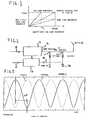
- Figure 1illustrates permitted nominal and actual loads directly on a final amplifier in a transmitter.
- the figureshows a nominal working line where the amplifier is subjected solely to resistive loads.
- Linear transmitter amplifiersare intended for a given nominal load, these amplifiers being able to deliver maximum output power and still remain linear (this includes feedback couplings and linearising couplings).
- the ratio Z 0 between voltage (U) and current (I)is precisely as illustrated by the nominal working line in Figure 1.
- the amplifierfunctions linearly along this line up to the maximum nominal power that can be outputted.
- Figure 2illustrates a coupling according to one preferred embodiment of the invention, where a transmitter 11 including at least one amplifying stage receives some form of input signal 10.
- This input signalmay be any type of signal whatsoever, although, in the case of the illustrated embodiment, it is assumed for the sake of simplicity that the signal is an RF signal that shall be amplified and then transmitted via an antenna/load 12.
- the antennathus functions as load and in this nature is a troublesome antenna since the load it represents and constantly sensed by the transmitter may vary significantly with time, as earlier mentioned.
- detector circuitmay be used to measure voltage and current on the transmitter output signal 13.
- a double diode detector 14that has two connection points 15 and 16 between transmitter 11 and load 12. It will be noted that any standard voltage meter whatsoever may be used to detect the voltage.
- the diode detectoris therefore merely an example of a simple and efficient voltage detector.
- connection points of the diode detector 14 between transmitter 11 and load 12are therefore positioned so that the distance between said connection points on the transmission line will correspond to +/- n*90 degrees (a quarter-wavelength) along said line so as to obtain two voltages, of which one corresponds to the output voltage and the other corresponds to the output current.
- One of the measuring pointsis therefore placed *180 degrees from the output.
- the figureshows the position of the detector between amplifier 11 and control circuit 17.
- Figure 3illustrates current and voltage between transmitter and load along the entire line between transmitter and load. It will be seen that current and voltage are mutually offset by 90 degrees at each given point between amplifier and load.
- the coupling illustrated in Figure 2 therewithgives an output voltage 13 which is determined by whether the voltage or Z 0 times the current in the amplifier is greatest at that moment in time, i.e. by which of the magnitudes I and U lie closest to their maximum (I max or U max ). The greatest of these magnitudes is determined by whether movement is along a load line that corresponds to low or high impedance in accordance with what is shown in Figure 1. Subsequent to rectification, this output voltage 13 thus constitutes the output signal from the detector 14 and is used as the real value 18 in an amplifier control coupling 17.
- a set-point value 19a signal that corresponds to the amplitude modulation envelope of the signal at that instance, multiplied by the gain of the amplifier at nominal load, so as to obtain the standard value at which the amplifier shall manage to operate in linear ranges.
- a comparisonis then made and the difference between real value and set-point value results in the signal 20 which is fed back into the transmitter. This signal then regulates the drive power for instance, and therewith the output amplitude of the amplifier.
- Quadrature modulationis one known method of generating linear modulation.
- Two baseband signalseach modulate a respective HF signal with respect to amplitude, where said signals are offset by 90 degrees in relation to each other.
- the modulated signalsare summated to obtain a desired signal that is phase-modulated and amplitude-modulated.
- a typical method of linearising of the amplification chain in a transmitter for quadrature modulationis to use quadrature feedback coupling.
- An HF signal from the amplifier outputis divided by down-mixing with HF signals offset through 90 degrees in quadrature components in the baseband.
- the quadrature componentsare then used as real values in amplitude feedback loops for corresponding modulating baseband signals.
- the signal to be returned from the transmitter output to the quadrature feedback circuitshould represent the voltage or current that is greatest in relation to its nominal value.
- Figure 4illustrates such an arrangement in which a chosen output signal 49 representing current or voltage from the transmitter amplifier chain 50 is fed back to the quadrature circuits 40.
- connection from the transmitter 50 to the load 51includes two lead terminals 41 and 42 and a detector circuit 48, which in a preferred embodiment comprises two diode detectors 43 and 44 that have a common output.
- One outputthus represents voltage on the amplifier output 52, while the other represents current.
- the voltage representing outputis referenced 42 and the current representing output is referenced 41.
- the detector circuit 48functions to supply a logic decision circuit 45 which controls a switch 46 to the outlet on the transmitter output that gives the highest detected voltage.
- the switch 46thus connects the measuring input of the quadrature feedback-coupling to the line outlet that has the highest amplitude, said detector output signal 49 being used as a real value in the transmitter.
- the arrangement that includes the switchsolves the problem of including the entire signal, which is necessary in respect of quadrature feedback-coupling, and not only the rectified variant which would have been the case if the detector circuit shown in Figure 2 had been used.
- the logic decision circuit 45may be a simple comparison circuit, i.e. a comparator. In order to obtain a decision circuit that functions smoothly, it is also conceivable to provide the diodes with given filtration with respect to amplitude detection. The embodiment shows that the same function as that obtained with the embodiment shown in Figure 2 can also be achieved with a quadrature feedback-coupled control system.
Landscapes
- Engineering & Computer Science (AREA)
- Power Engineering (AREA)
- Physics & Mathematics (AREA)
- Nonlinear Science (AREA)
- Transmitters (AREA)
- Amplifiers (AREA)
- Toys (AREA)
- Massaging Devices (AREA)
- Finger-Pressure Massage (AREA)
Abstract
Description
- Figure 1 is an electric current-voltage diagramillustrating different types of load impedances;
- Figure 2 is a coupling diagram corresponding topreferred embodiments;
- Figure 3 illustrates how current and voltage behavealong an electric conductor; and
- Figure 4 is a coupling diagram illustrating analternative embodiment.
Claims (9)
- An arrangement for transmitting and amplifying aninput signal, comprising a transmitter (11; 50) and a load(12; 51) connected to the transmitter,characterisedin that the arrangement also includesa detector circuit (14; 48) between transmitter(11; 50) and load (12; 51) for identifying which of theoutput current and the output voltage lies closest to itsmaximum value and for delivering a detector output signal(18; 49) corresponding to which of the voltage or thecurrent on the transmitter output (13; 52) which liesclosest to its respective maximum value at a certain momentin time, wherein the detector output signal (18; 49) isapplied to a control system (17; 40) for feedback of thedetector output signal to the transmitter (11; 50) andwherein the control system includes means for regulatingthe output signal of the transmitter (11; 50) by means ofthe detector output signal.
- An arrangement for transmitting and amplifying aninput signal in accordance with claim 1,
characterised in that the detector circuit (14; 48)is connected to two measuring points (15, 16; 41, 42) onthe transmission line between transmitter and load (12; 51)for the purpose of measuring two voltage amplitudes at saidtwo measuring points, one of said voltage amplitudesrepresenting the output voltage and the other representingthe output current. - An arrangement for transmitting and amplifying aninput signal in accordance with claim 2,
characterised in that said measuring points (15, 16;41, 42) are located at an electric distance from each otherthat corresponds to a quarter wavelength or to an odd multiple thereof, and a distance from one of the points tothe transmitter output that corresponds to a multiple ofone-half wavelength, including the multiple zero. - An arrangement for transmitting and amplifying aninput signal according to any one of claims 1-3,
characterised in that the detector output signal (18;49) is used as a real value. - An arrangement for transmitting and amplifying aninput signal according to any one of claims 1-4,
characterised in that the arrangement includesa quadrature feedback-coupled regulating system(40) for regulating the transmitter output signal;a decision circuit (45) included in the detectorcircuit (48) for identifying and deciding whether thevoltage or the current on the transmitter output (52) hasthe greatest amplitude, wherewith the output signal of thedecision circuit functions to controla switch (46) to couple the chosen transmitteroutput signal (49) to said regulating system (40) as a realvalue. - An arrangement for transmitting and amplifying aninput signal in an arrangement in accordance with claim 5,
characterised in that the detector circuit includestwo diode detectors (43, 44) having a common output. - A method of transmitting and amplifying an inputsignal in an arrangement that includes a transmitter (11;50) and a load (12; 51) connected to the transmitter,
characterised by determining whether the voltage orthe current on the transmitter output (13; 52) lies closestto its respective maximum value at a certain moment intime, and feeding the value which lies closest to its maximum back to the transmitter via a regulating system(17; 40) for regulating the output signal of thetransmitter (11; 40) by means of the detected signal. - A method of transmitting and amplifying an inputsignal in accordance with claim 7,characterised bydetecting two voltage amplitudes on the transmission linebetween transmitter and load at two measuring points (15,16; 41, 42), wherewith one represents the output voltageand the other represents the output current.
- A method of transmitting and amplifying an inputsignal in accordance with claim 8,characterised byselecting said measuring points (15, 16; 41, 42) at anelectric distance from each other that corresponds to aquarter wavelength or to an odd multiple thereof, and at adistance from one of said points to the transmitter outputcorresponding to a multiple of a half wavelength, includingthe multiple zero.
Applications Claiming Priority (5)
| Application Number | Priority Date | Filing Date | Title |
|---|---|---|---|
| SE0102346ASE520539C2 (en) | 2001-06-29 | 2001-06-29 | Input signal transmitting and amplifying arrangement has detector circuit producing output signal of voltage or current which lies closest to maximum value to be fed to control system for feedback to transmitter |
| SE0102346 | 2001-06-29 | ||
| US30466401P | 2001-07-11 | 2001-07-11 | |
| US304664P | 2001-07-11 | ||
| PCT/EP2002/006951WO2003003565A2 (en) | 2001-06-29 | 2002-06-24 | A transmitter control circuit |
Publications (2)
| Publication Number | Publication Date |
|---|---|
| EP1400011A2 EP1400011A2 (en) | 2004-03-24 |
| EP1400011B1true EP1400011B1 (en) | 2005-12-14 |
Family
ID=26655506
Family Applications (1)
| Application Number | Title | Priority Date | Filing Date |
|---|---|---|---|
| EP02747424AExpired - LifetimeEP1400011B1 (en) | 2001-06-29 | 2002-06-24 | A transmitter control circuit |
Country Status (6)
| Country | Link |
|---|---|
| US (1) | US7209718B2 (en) |
| EP (1) | EP1400011B1 (en) |
| AT (1) | ATE313167T1 (en) |
| AU (1) | AU2002317839A1 (en) |
| DE (1) | DE60208027D1 (en) |
| WO (1) | WO2003003565A2 (en) |
Families Citing this family (3)
| Publication number | Priority date | Publication date | Assignee | Title |
|---|---|---|---|---|
| US20050255812A1 (en)* | 2004-05-17 | 2005-11-17 | Samsung Electronics Co., Ltd. | RF front-end apparatus in a TDD wireless communication system |
| US7787839B2 (en)* | 2006-12-06 | 2010-08-31 | Broadcom Corporation | RFIC with dynamically controlled power amplifier |
| US8606200B2 (en)* | 2007-06-26 | 2013-12-10 | Intel Corporation | Error vector magnitude control within a linear transmitter |
Family Cites Families (12)
| Publication number | Priority date | Publication date | Assignee | Title |
|---|---|---|---|---|
| US4066965A (en)* | 1976-09-28 | 1978-01-03 | The United States Of America As Represented By The Secretary Of The Navy | RF GTWT Saturating circuit |
| US4547746A (en)* | 1984-04-09 | 1985-10-15 | Rockwell International Corporation | VSWR Tolerant linear power amplifier |
| GB2158620A (en) | 1984-05-08 | 1985-11-13 | Philips Electronic Associated | Power control for radio transmitters |
| US4673886A (en)* | 1986-02-26 | 1987-06-16 | Motorola, Inc. | Adaptively stabilized RF amplifier |
| US5257415A (en)* | 1991-03-20 | 1993-10-26 | Fujitsu Limited | Automatic transmission level control device |
| JP2871889B2 (en)* | 1991-04-16 | 1999-03-17 | 三菱電機株式会社 | High frequency power amplifier |
| TW225619B (en)* | 1991-07-19 | 1994-06-21 | Nippon Electric Co | |
| US5287555A (en)* | 1991-07-22 | 1994-02-15 | Motorola, Inc. | Power control circuitry for a TDMA radio frequency transmitter |
| US5206600A (en)* | 1991-10-18 | 1993-04-27 | Harris Corporation | Impedance determining apparatus using quadrature current and peak detectors |
| US5300894A (en)* | 1992-10-20 | 1994-04-05 | At&T Bell Laboratories | Circuitry for minimizing peak power in an amplifier carrying a plurality of signals of differing frequencies |
| JPH08149021A (en)* | 1994-11-22 | 1996-06-07 | Nec Yamagata Ltd | Receiver front-end circuit |
| US5894496A (en)* | 1996-09-16 | 1999-04-13 | Ericsson Inc. | Method and apparatus for detecting and compensating for undesired phase shift in a radio transceiver |
- 2002
- 2002-06-24AUAU2002317839Apatent/AU2002317839A1/ennot_activeAbandoned
- 2002-06-24EPEP02747424Apatent/EP1400011B1/ennot_activeExpired - Lifetime
- 2002-06-24USUS10/481,188patent/US7209718B2/ennot_activeExpired - Lifetime
- 2002-06-24ATAT02747424Tpatent/ATE313167T1/ennot_activeIP Right Cessation
- 2002-06-24WOPCT/EP2002/006951patent/WO2003003565A2/ennot_activeApplication Discontinuation
- 2002-06-24DEDE60208027Tpatent/DE60208027D1/ennot_activeExpired - Lifetime
Also Published As
| Publication number | Publication date |
|---|---|
| AU2002317839A1 (en) | 2003-03-03 |
| WO2003003565A2 (en) | 2003-01-09 |
| WO2003003565A3 (en) | 2003-09-04 |
| US20040176153A1 (en) | 2004-09-09 |
| EP1400011A2 (en) | 2004-03-24 |
| ATE313167T1 (en) | 2005-12-15 |
| DE60208027D1 (en) | 2006-01-19 |
| US7209718B2 (en) | 2007-04-24 |
Similar Documents
| Publication | Publication Date | Title |
|---|---|---|
| US6297696B1 (en) | Optimized power amplifier | |
| US7482873B2 (en) | Preserving linearity of a rf power amplifier | |
| CN1871791B (en) | Additional Adjustment of Reference Signals for Automatic Power Control in Mobile Terminals | |
| JP3568994B2 (en) | Directional detector for power level control | |
| US7512386B2 (en) | Method and apparatus providing integrated load matching using adaptive power amplifier compensation | |
| EP0458071B1 (en) | VSWR adaptive power amplifier system | |
| US6301486B1 (en) | Radio telephone apparatus | |
| US8274333B2 (en) | Method and apparatus for protecting devices in an RF power amplifier | |
| US5678209A (en) | Transmit power level detection circuit with enhanced gain characteristics | |
| CA1091776A (en) | Power amplifier arrangement automatically matched to service conditions | |
| US8644776B1 (en) | Systems and methods for providing improved power performance in wireless communication systems | |
| US5913154A (en) | VSWR control technique for terminal products with linear modulation | |
| JP2006217362A (en) | Limiter circuit | |
| EP1400011B1 (en) | A transmitter control circuit | |
| US20080002787A1 (en) | Method to maintain RF power amplifier linearity in varying load VSWR conditions without isolator | |
| EP1709731B1 (en) | Electronic circuit | |
| SE520539C2 (en) | Input signal transmitting and amplifying arrangement has detector circuit producing output signal of voltage or current which lies closest to maximum value to be fed to control system for feedback to transmitter | |
| US6999524B1 (en) | Arrangement for controlling the output power of an HF transmitter | |
| KR0141434B1 (en) | Multi-radio transmitter | |
| US20010028252A1 (en) | Impedance adapting circuit | |
| CN110880918A (en) | Power amplifier circuit and interphone thereof | |
| JPH0577221B2 (en) |
Legal Events
| Date | Code | Title | Description |
|---|---|---|---|
| PUAI | Public reference made under article 153(3) epc to a published international application that has entered the european phase | Free format text:ORIGINAL CODE: 0009012 | |
| 17P | Request for examination filed | Effective date:20031114 | |
| AK | Designated contracting states | Kind code of ref document:A2 Designated state(s):AT BE CH CY DE DK ES FI FR GB GR IE IT LI LU MC NL PT SE TR | |
| AX | Request for extension of the european patent | Extension state:AL LT LV MK RO SI | |
| RAP1 | Party data changed (applicant data changed or rights of an application transferred) | Owner name:TELEFONAKTIEBOLAGET LM ERICSSON (PUBL) | |
| 17Q | First examination report despatched | Effective date:20040723 | |
| GRAP | Despatch of communication of intention to grant a patent | Free format text:ORIGINAL CODE: EPIDOSNIGR1 | |
| GRAS | Grant fee paid | Free format text:ORIGINAL CODE: EPIDOSNIGR3 | |
| GRAA | (expected) grant | Free format text:ORIGINAL CODE: 0009210 | |
| AK | Designated contracting states | Kind code of ref document:B1 Designated state(s):AT BE CH CY DE DK ES FI FR GB GR IE IT LI LU MC NL PT SE TR | |
| PG25 | Lapsed in a contracting state [announced via postgrant information from national office to epo] | Ref country code:IT Free format text:LAPSE BECAUSE OF FAILURE TO SUBMIT A TRANSLATION OF THE DESCRIPTION OR TO PAY THE FEE WITHIN THE PRESCRIBED TIME-LIMIT;WARNING: LAPSES OF ITALIAN PATENTS WITH EFFECTIVE DATE BEFORE 2007 MAY HAVE OCCURRED AT ANY TIME BEFORE 2007. THE CORRECT EFFECTIVE DATE MAY BE DIFFERENT FROM THE ONE RECORDED. Effective date:20051214 Ref country code:FI Free format text:LAPSE BECAUSE OF FAILURE TO SUBMIT A TRANSLATION OF THE DESCRIPTION OR TO PAY THE FEE WITHIN THE PRESCRIBED TIME-LIMIT Effective date:20051214 Ref country code:AT Free format text:LAPSE BECAUSE OF FAILURE TO SUBMIT A TRANSLATION OF THE DESCRIPTION OR TO PAY THE FEE WITHIN THE PRESCRIBED TIME-LIMIT Effective date:20051214 Ref country code:BE Free format text:LAPSE BECAUSE OF FAILURE TO SUBMIT A TRANSLATION OF THE DESCRIPTION OR TO PAY THE FEE WITHIN THE PRESCRIBED TIME-LIMIT Effective date:20051214 Ref country code:CH Free format text:LAPSE BECAUSE OF FAILURE TO SUBMIT A TRANSLATION OF THE DESCRIPTION OR TO PAY THE FEE WITHIN THE PRESCRIBED TIME-LIMIT Effective date:20051214 Ref country code:NL Free format text:LAPSE BECAUSE OF FAILURE TO SUBMIT A TRANSLATION OF THE DESCRIPTION OR TO PAY THE FEE WITHIN THE PRESCRIBED TIME-LIMIT Effective date:20051214 Ref country code:LI Free format text:LAPSE BECAUSE OF FAILURE TO SUBMIT A TRANSLATION OF THE DESCRIPTION OR TO PAY THE FEE WITHIN THE PRESCRIBED TIME-LIMIT Effective date:20051214 | |
| REG | Reference to a national code | Ref country code:GB Ref legal event code:FG4D | |
| REG | Reference to a national code | Ref country code:CH Ref legal event code:EP | |
| REG | Reference to a national code | Ref country code:IE Ref legal event code:FG4D | |
| REF | Corresponds to: | Ref document number:60208027 Country of ref document:DE Date of ref document:20060119 Kind code of ref document:P | |
| PG25 | Lapsed in a contracting state [announced via postgrant information from national office to epo] | Ref country code:DK Free format text:LAPSE BECAUSE OF FAILURE TO SUBMIT A TRANSLATION OF THE DESCRIPTION OR TO PAY THE FEE WITHIN THE PRESCRIBED TIME-LIMIT Effective date:20060314 Ref country code:GR Free format text:LAPSE BECAUSE OF FAILURE TO SUBMIT A TRANSLATION OF THE DESCRIPTION OR TO PAY THE FEE WITHIN THE PRESCRIBED TIME-LIMIT Effective date:20060314 Ref country code:SE Free format text:LAPSE BECAUSE OF FAILURE TO SUBMIT A TRANSLATION OF THE DESCRIPTION OR TO PAY THE FEE WITHIN THE PRESCRIBED TIME-LIMIT Effective date:20060314 | |
| PG25 | Lapsed in a contracting state [announced via postgrant information from national office to epo] | Ref country code:DE Free format text:LAPSE BECAUSE OF FAILURE TO SUBMIT A TRANSLATION OF THE DESCRIPTION OR TO PAY THE FEE WITHIN THE PRESCRIBED TIME-LIMIT Effective date:20060315 | |
| PG25 | Lapsed in a contracting state [announced via postgrant information from national office to epo] | Ref country code:ES Free format text:LAPSE BECAUSE OF FAILURE TO SUBMIT A TRANSLATION OF THE DESCRIPTION OR TO PAY THE FEE WITHIN THE PRESCRIBED TIME-LIMIT Effective date:20060325 | |
| PG25 | Lapsed in a contracting state [announced via postgrant information from national office to epo] | Ref country code:PT Free format text:LAPSE BECAUSE OF FAILURE TO SUBMIT A TRANSLATION OF THE DESCRIPTION OR TO PAY THE FEE WITHIN THE PRESCRIBED TIME-LIMIT Effective date:20060515 | |
| NLV1 | Nl: lapsed or annulled due to failure to fulfill the requirements of art. 29p and 29m of the patents act | ||
| PG25 | Lapsed in a contracting state [announced via postgrant information from national office to epo] | Ref country code:GB Free format text:LAPSE BECAUSE OF NON-PAYMENT OF DUE FEES Effective date:20060624 | |
| PG25 | Lapsed in a contracting state [announced via postgrant information from national office to epo] | Ref country code:IE Free format text:LAPSE BECAUSE OF NON-PAYMENT OF DUE FEES Effective date:20060626 | |
| PG25 | Lapsed in a contracting state [announced via postgrant information from national office to epo] | Ref country code:MC Free format text:LAPSE BECAUSE OF NON-PAYMENT OF DUE FEES Effective date:20060630 | |
| REG | Reference to a national code | Ref country code:CH Ref legal event code:PL | |
| ET | Fr: translation filed | ||
| PLBE | No opposition filed within time limit | Free format text:ORIGINAL CODE: 0009261 | |
| STAA | Information on the status of an ep patent application or granted ep patent | Free format text:STATUS: NO OPPOSITION FILED WITHIN TIME LIMIT | |
| 26N | No opposition filed | Effective date:20060915 | |
| GBPC | Gb: european patent ceased through non-payment of renewal fee | Effective date:20060624 | |
| PG25 | Lapsed in a contracting state [announced via postgrant information from national office to epo] | Ref country code:LU Free format text:LAPSE BECAUSE OF NON-PAYMENT OF DUE FEES Effective date:20060624 Ref country code:TR Free format text:LAPSE BECAUSE OF FAILURE TO SUBMIT A TRANSLATION OF THE DESCRIPTION OR TO PAY THE FEE WITHIN THE PRESCRIBED TIME-LIMIT Effective date:20051214 | |
| PG25 | Lapsed in a contracting state [announced via postgrant information from national office to epo] | Ref country code:CY Free format text:LAPSE BECAUSE OF FAILURE TO SUBMIT A TRANSLATION OF THE DESCRIPTION OR TO PAY THE FEE WITHIN THE PRESCRIBED TIME-LIMIT Effective date:20051214 | |
| REG | Reference to a national code | Ref country code:FR Ref legal event code:PLFP Year of fee payment:15 | |
| REG | Reference to a national code | Ref country code:FR Ref legal event code:PLFP Year of fee payment:16 | |
| REG | Reference to a national code | Ref country code:FR Ref legal event code:PLFP Year of fee payment:17 | |
| PGFP | Annual fee paid to national office [announced via postgrant information from national office to epo] | Ref country code:FR Payment date:20180626 Year of fee payment:17 | |
| PG25 | Lapsed in a contracting state [announced via postgrant information from national office to epo] | Ref country code:FR Free format text:LAPSE BECAUSE OF NON-PAYMENT OF DUE FEES Effective date:20190630 |