EP1393166B1 - Dynamically reconfigurable data space - Google Patents
Dynamically reconfigurable data spaceDownload PDFInfo
- Publication number
- EP1393166B1 EP1393166B1EP02752011AEP02752011AEP1393166B1EP 1393166 B1EP1393166 B1EP 1393166B1EP 02752011 AEP02752011 AEP 02752011AEP 02752011 AEP02752011 AEP 02752011AEP 1393166 B1EP1393166 B1EP 1393166B1
- Authority
- EP
- European Patent Office
- Prior art keywords
- memory
- instruction
- dsp
- data
- dual
- Prior art date
- Legal status (The legal status is an assumption and is not a legal conclusion. Google has not performed a legal analysis and makes no representation as to the accuracy of the status listed.)
- Expired - Lifetime
Links
Images


Classifications
- G—PHYSICS
- G06—COMPUTING OR CALCULATING; COUNTING
- G06F—ELECTRIC DIGITAL DATA PROCESSING
- G06F9/00—Arrangements for program control, e.g. control units
- G06F9/06—Arrangements for program control, e.g. control units using stored programs, i.e. using an internal store of processing equipment to receive or retain programs
- G06F9/30—Arrangements for executing machine instructions, e.g. instruction decode
- G06F9/34—Addressing or accessing the instruction operand or the result ; Formation of operand address; Addressing modes
- G06F9/342—Extension of operand address space
- G—PHYSICS
- G06—COMPUTING OR CALCULATING; COUNTING
- G06F—ELECTRIC DIGITAL DATA PROCESSING
- G06F12/00—Accessing, addressing or allocating within memory systems or architectures
- G06F12/02—Addressing or allocation; Relocation
- G06F12/0223—User address space allocation, e.g. contiguous or non contiguous base addressing
- G06F12/0284—Multiple user address space allocation, e.g. using different base addresses
- G—PHYSICS
- G06—COMPUTING OR CALCULATING; COUNTING
- G06F—ELECTRIC DIGITAL DATA PROCESSING
- G06F12/00—Accessing, addressing or allocating within memory systems or architectures
- G06F12/02—Addressing or allocation; Relocation
- G06F12/08—Addressing or allocation; Relocation in hierarchically structured memory systems, e.g. virtual memory systems
- G06F12/0802—Addressing of a memory level in which the access to the desired data or data block requires associative addressing means, e.g. caches
- G06F12/0806—Multiuser, multiprocessor or multiprocessing cache systems
- G06F12/0815—Cache consistency protocols
- G06F12/0831—Cache consistency protocols using a bus scheme, e.g. with bus monitoring or watching means
- G—PHYSICS
- G06—COMPUTING OR CALCULATING; COUNTING
- G06F—ELECTRIC DIGITAL DATA PROCESSING
- G06F12/00—Accessing, addressing or allocating within memory systems or architectures
- G06F12/02—Addressing or allocation; Relocation
- G06F12/08—Addressing or allocation; Relocation in hierarchically structured memory systems, e.g. virtual memory systems
- G06F12/10—Address translation
- G06F12/109—Address translation for multiple virtual address spaces, e.g. segmentation
- G—PHYSICS
- G06—COMPUTING OR CALCULATING; COUNTING
- G06F—ELECTRIC DIGITAL DATA PROCESSING
- G06F9/00—Arrangements for program control, e.g. control units
- G06F9/06—Arrangements for program control, e.g. control units using stored programs, i.e. using an internal store of processing equipment to receive or retain programs
- G06F9/30—Arrangements for executing machine instructions, e.g. instruction decode
- G06F9/30181—Instruction operation extension or modification
- G06F9/30185—Instruction operation extension or modification according to one or more bits in the instruction, e.g. prefix, sub-opcode
- G—PHYSICS
- G06—COMPUTING OR CALCULATING; COUNTING
- G06F—ELECTRIC DIGITAL DATA PROCESSING
- G06F9/00—Arrangements for program control, e.g. control units
- G06F9/06—Arrangements for program control, e.g. control units using stored programs, i.e. using an internal store of processing equipment to receive or retain programs
- G06F9/30—Arrangements for executing machine instructions, e.g. instruction decode
- G06F9/34—Addressing or accessing the instruction operand or the result ; Formation of operand address; Addressing modes
- G06F9/345—Addressing or accessing the instruction operand or the result ; Formation of operand address; Addressing modes of multiple operands or results
Definitions
- the present inventionrelates to systems and methods for addressing memory locations and, more particularly, to systems and methods for dynamically accessing a memory as a linear memory space and as a dual memory space.
- DSPsDigital Signal Processors
- the calculationsmay include repetitive operations such as multiply and accumulate operations that are performed on a series of constant or calculated data stored in a memory.
- DSPsmust be able to repetitively fetch two operands for immediate processing, calculate a result and write the result back within one processor cycle.
- result write backshould occur at the end of each processor cycle once the pipeline is full.
- DSPstypically have the ability to perform dual concurrent operand fetches from a relatively large data memory.
- Conventional microcontrollers and microprocessorstypically allow dual concurrent operand fetches only from a limited number registers, which is overly restrictive for DSPs. This is because processor cycles must be devoted to loading registers with operand data as an intermediate step prior to processing the data, rather than fetching the operand data directly from the memory in the case of a DSP.
- DSPstypically include two data memories, an X memory and a Y memory. They further include X and Y data buses coupled respectively to the X and Y memories. The X and Y memories are separately addressed and allow the DSP to perform dual, concurrent operand fetching and processing directly from the memories-one operand being fetched from the X memory and the other from the Y memory.
- a processor capable of performing DSP operations and controller operationsis known from "A RISC Architecture with uncompromised Digital Signal Processing and Microcontroller Operation", by Daniel Martin in Proceedings of the 1998 IEEE International Conference, published12 May 1998, pages 3097-3100 , XP010279502ISBN.
- US 5,832,257discloses a digital signal processing system for executing instructions and processing data, including a program memory which stores the instructions and a first portion of the data, a data memory which stores a second portion of the data, and a program control unit connected to the program memory for receiving a sequence of the instructions and generating control signals for executing the instructions.
- a processorhas a data memory that may be addressed as a dual memory space in one mode and as a single linear memory space in another mode.
- the memorymay permit dual concurrent operand fetches from the data memory when DSP instructions are processed.
- the memorymay then dynamically permit the same memory to be accessed as a single linear memory address space for non-DSP instructions.
- the methodprovides linear and dual address spaces within a memory.
- the methodincludes providing a digital signal processor (DSP) engine, an arithmetic logic unit (ALU) and a memory.
- the methodfurther includes providing separate X and Y address generation units for generating addresses to the memory.
- the X address generation unitmay be configured to generate addresses to all of the memory space when processing a non-digital signal processor (DSP) engine instruction and to a first portion of the memory when processing a DSP engine instruction.
- the Y address generation unitmay be configured to generate addresses to a second portion of the memory space when processing a DSP engine instruction and to none of the memory space when processing a non-digital signal processor (DSP) engine instruction.
- the methodmay further include providing an instruction decoder that decodes instructions and, in response, activates the X address generation unit for ALU instructions and activates the X and Y address generation units for DSP engine instructions.
- the first and second memory portionsmay be overlapping or non-overlapping.
- the first and second portion memory portionsmay further be contiguous or not contiguous with respect to each other.
- the first portionmay include a portion above the second portion and a portion below the second portion.
- the methodmay further include providing separate X and Y data buses.
- the X data busmay be coupled to the memory permitting reading and writing to and from the entire memory and the Y data bus may be coupled to the second portion of the memory permitting reading and also writing in some embodiments from the second portion.
- the methodmay further include reading X and Y operands concurrently from the respective first and second portions of the memory over the X and Y data buses based on the instruction decoder decoding a DSP instruction requiring a dual operand fetch.
- a processoraddresses a memory as a signal and dual space memory based on an addressing mode.
- the processorincludes a data memory, an instruction decoder and X and Y address generators.
- the data memoryhas X and Y memory spaces.
- the instruction decoderdetermines whether an instruction requires single or dual memory space operation and selectively activates the X and Y address generators.
- the instruction decoderactivates the X and Y address generators based on the instruction decoder determining dual memory space operation is required.
- the instruction decoderactivates the X address generator only based on the instruction decoder determining single memory space operation is required.
- the processormay further include registers coupled to the X and Y address generators for storing pointers to the memory. For a dual memory space operation, a subset of the registers stores pointers to the Y space within the memory and a subset of the registers stores pointers to the X space within the memory. For a single memory space operation, any of the registers stores pointers to the memory.
- the processormay further include X and Y data buses coupled to the memory for retrieving operands from the X and Y memory spaces in a dual memory space operation and for retrieving operands from the memory over the X data bus in a single memory space operation.
- the processormay further include a DSP engine having operand inputs coupled to the X and Y data buses and having a result output coupled only to the X data bus.
- the processormay still further include an arithmetic logic unit (ALU) coupled to the X data buses for operand and result input and output.
- ALUarithmetic logic unit
- a processorhas a data memory that may be addressed as a dual memory space in one mode and as a single linear memory space in another mode.
- the memorymay permit dual concurrent operand fetches from the data memory when DSP instructions are processed.
- the memorymay then dynamically permit the same memory to be accessed as a single linear memory address space for non-DSP instructions.
- FIGS. 1 and 2In order to describe embodiments of processing instructions in word and/or byte modes, an overview of pertinent processor elements is first presented with reference to FIGS. 1 and 2 . The systems and methods for implementing word and/or byte mode processing are then described more particularly with reference to FIGS. 3-5 .
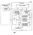
- FIG. 1depicts a functional block diagram of an embodiment of a processor chip within which the present invention may find application.
- a processor 100is coupled to external devices/systems 140.
- the processor 100may be any type of processor including, for example, a digital signal processor (DSP), a microprocessor, a microcontroller or combinations thereof.
- the external devices 140may be any type of systems or devices including input/output devices such as keyboards, displays, speakers, microphones, memory, or other systems which may or may not include processors.
- the processor 100 and the external devices 140may together comprise a stand alone system.
- the processor 100includes a program memory 105, an instruction fetch/decode unit 110, instruction execution units 115, data memory and registers 120, peripherals 125, data I/O 130, and a program counter and loop control unit 135.
- the bus 150which may include one or more common buses, communicates data between the units as shown.
- the program memory 105stores software embodied in program instructions for execution by the processor 100.
- the program memory 105may comprise any type of nonvolatile memory such as a read only memory (ROM), a programmable read only memory (PROM), an electrically programmable or an electrically programmable and erasable read only memory (EPROM or EEPROM) or flash memory.
- ROMread only memory
- PROMprogrammable read only memory
- EPROM or EEPROMelectrically programmable and erasable read only memory
- flash memoryflash memory
- the program memory 105may be supplemented with external nonvolatile memory 145 as shown to increase the complexity of software available to the processor 100.
- the program memorymay be volatile memory which receives program instructions from, for example, an external non-volatile memory 145.
- the program memory 105When the program memory 105 is nonvolatile memory, the program memory may be programmed at the time of manufacturing the processor 100 or prior to or during implementation of the processor 100 within a system. In the latter scenario, the processor 100 may be programmed through a process called inline serial programming.
- the instruction fetch/decode unit 110is coupled to the program memory 105, the instruction execution units 115 and the data memory 120. Coupled to the program memory 105 and the bus 150 is the program counter and loop control unit 135. The instruction fetch/decode unit 110 fetches the instructions from the program memory 105 specified by the address value contained in the program counter 135. The instruction fetch/decode unit 110 then decodes the fetched instructions and sends the decoded instructions to the appropriate execution unit 115. The instruction fetch/decode unit 110 may also send operand information including addresses of data to the data memory 120 and to functional elements that access the registers.
- the program counter and loop control unit 135includes a program counter register (not shown) which stores an address of the next instruction to be fetched. During normal instruction processing, the program counter register may be incremented to cause sequential instructions to be fetched. Alternatively, the program counter value may be altered by loading a new value into it via the bus 150. The new value may be derived based on decoding and executing a flow control instruction such as, for example, a branch instruction. In addition, the loop control portion of the program counter and loop control unit 135 may be used to provide repeat instruction processing and repeat loop control as further described below.
- the instruction execution units 115receive the decoded instructions from the instruction fetch/decode unit 110 and thereafter execute the decoded instructions. As part of this process, the execution units may retrieve one or two operands via the bus 150 and store the result into a register or memory location within the data memory 120.
- the execution unitsmay include an arithmetic logic unit (ALU) such as those typically found in a microcontroller.
- ALUarithmetic logic unit
- the execution unitsmay also include a digital signal processing engine, a floating point processor, an integer processor or any other convenient execution unit.
- a preferred embodiment of the execution units and their interaction with the bus 150, which may include one or more buses,is presented in more detail below with reference to FIG. 2 .
- the data memory and registers 120are volatile memory and are used to store data used and generated by the execution units.
- the data memory 120 and program memory 105are preferably separate memories for storing data and program instructions respectively.
- This formatis a known generally as a Harvard architecture. It is noted, however, that according to the present invention, the architecture may be a Von-Neuman architecture or a modified Harvard architecture which permits the use of some program space for data space.
- a dotted lineis shown, for example, connecting the program memory 105 to the bus 150. This path may include logic for aligning data reads from program space such as, for example, during table reads from program space to data memory 120.
- a plurality of peripherals 125 on the processormay be coupled to the bus 125.
- the peripheralsmay include, for example, analog to digital converters, timers, bus interfaces and protocols such as, for example, the controller area network (CAN) protocol or the Universal Serial Bus (USB) protocol and other peripherals.
- the peripheralsexchange data over the bus 150 with the other units.
- the data I/O unit 130may include transceivers and other logic for interfacing with the external devices/systems 140.
- the data I/O unit 130may further include functionality to permit in circuit serial programming of the Program memory through the data I/O unit 130.
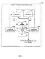
- FIG. 2depicts a functional block diagram of a data busing scheme for use in a processor 100, such as that shown in FIG. 1 , which has an integrated microcontroller arithmetic logic unit (ALU) 270 and a digital signal processing (DSP) engine 230.
- ALUmicrocontroller arithmetic logic unit
- DSPdigital signal processing
- This configurationmay be used to integrate DSP functionality to an existing microcontroller core.
- the data memory 120 of FIG. 1is implemented as two separate memories: an X-memory 210 and a Y-memory 220, each being respectively addressable by an X-address generator 250 and a Y-address generator 260.
- the X-address generatormay also permit addressing the Y-memory space thus making the data space appear like a single contiguous memory space when addressed from the X address generator.
- the bus 150may be implemented as two buses, one for each of the X and Y memory, to permit simultaneous fetching of data from the X and Y memories.
- the W registers 240are general purpose address and/or data registers.
- the DSP engine 230is coupled to both the X and Y memory buses and to the W registers 240.
- the DSP engine 230may simultaneously fetch data from each the X and Y memory, execute instructions which operate on the simultaneously fetched data and write the result to an accumulator (not shown) and write a prior result to X or Y memory or to the W registers 240 within a single processor cycle.
- the ALU 270may be coupled only to the X memory bus and may only fetch data from the X bus.
- the X and Y memories 210 and 220may be addressed as a single memory space by the X address generator in order to make the data memory segregation transparent to the ALU 270.
- the memory locations within the X and Y memoriesmay be addressed by values stored in the W registers 240.
- processor clocking schememay be implemented for fetching and executing instructions.
- a specific examplefollows, however, to illustrate an embodiment of the present invention.
- Each instruction cycleis comprised of four Q clock cycles Q1-Q4.
- the four phase Q cyclesprovide timing signals to coordinate the decode, read, process data and write data portions of each instruction cycle.
- the processor 100concurrently performs two operations-it fetches the next instruction and executes the present instruction. Accordingly, the two processes occur simultaneously.
- the following sequence of eventsmay comprise, for example, the fetch instruction cycle:
- sequence of eventsmay comprise, for example, the execute instruction cycle for a single operand instruction:
- the following sequence of eventsmay comprise, for example, the execute instruction cycle for a dual operand instruction using a data pre-fetch mechanism. These instructions prefetch the dual operands simultaneously from the X and Y data memories and store them into registers specified in the instruction. They simultaneously allow instruction execution on the operands fetched during the previous cycle.
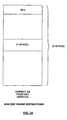
- FIGS. 3A and 3Bdepict an organization of the data memory 120 according to an embodiment of the present invention.
- the data memory 120may be organized as a contiguous memory that includes an X space portion and a Y space portion.
- the processoris processing a non-DSP engine instruction
- only the X address generator 250is active. In this mode, the entire memory may be accessed using the X address generator. Accordingly, data may be read from the entire memory and written into the entire memory 120, including the Y space portion thereof, using the X address generator. This permits the data memory 120 to be accessed as a linear address space during non-DSP engine instruction processing.
- the data memory 120is defined to have separate X and Y spaces.
- the X and Y spaceare separately addressable by the X address generator and the Y address generator.
- the X address generatorgenerates addresses for the X portion of the data memory and the Y address generator only generates addresses for the Y portion of the data memory.
- the X and Y spacesmay each be less than the entire memory and in a preferred embodiment the X space includes portions above and below the Y space portion.
- the instruction decodergenerates control signals, based on the decoded instruction which determine the addressing mode, for activating the X address generator 250 and the Y address generator 260.
- the instruction decoderdecodes a non-DSP engine instruction
- the instruction decodergenerates control signals which disable the y-address generator 260 and the y-data bus.
- the instruction decoderalso generates control signals that allow any of the registers 240 to include a pointer value to any location within the data memory 120.
- instruction processingmay entail addressing the data memory as a linear address space via the X address generator to a) fetch operands from the memory 120, b) execute the instruction on the operands and c) store back the result into the data memory over the x-data bus into a memory location specified to the X address generator 250.
- the instruction decoderWhen the instruction decoder decodes a DSP engine instruction, the instruction decoder generates control signals which enable the y-address generator 260 and the y-data bus.
- the instruction decodermay configure the x-address generator 250 and the y-address generator 260 to only accept indirect addresses from certain registers within the W array 240.
- the x-address generator and the y-address generatorare each configured to only process indirect addresses from a respective four of the W-registers 240 with two being different for X address generation and 2 different ones being for Y address generation. However, any number of registers may be allocated for these purposes.
- the instruction decoderdecodes the DSP engine instruction and causes the DSP engine to fetch and process two operands simultaneously from the data memory 120.
- One of the operandsis fetched from the y-data space over the y-data bus based on a pointer address specified in one of two of the designated W registers 240 and decoded by the Y address generator.
- the other operandis fetched from the x-data space over the x-data bus based on a pointer address specified in one of the designated W registers 240 and decoded by the X address generator.
- the X and Y spacesmay be non-overlapping and contiguous. Alternatively, the X and Y spaces may be overlapping.
- FIG. 4depicts a method of dynamically reconfiguring a memory to permit addressing the memory as a dual memory or as a memory with a single linear address space according to an embodiment of the present invention.
- a DSP enginean arithmetic logic unit (ALU) and a memory are provided on a processor.
- ALUarithmetic logic unit
- This configurationmay permit the processor to process DSP instructions in addition to microcontroller or microprocessor instructions and may further permit the melding of two instructions sets or an expanded instruction set within the same processor.
- step 405separate X and Y space address generators are provided for addressing portions of the memory as two separate X and Y memory spaces in one mode and for addressing the entire memory as a single linear address space using the X address generator in another mode.
- the X and Y address generatorsmay be configured at the time of manufacturing the processor to set the portions addressable by the X and Y address generators in the dual memory space mode.
- the X and Y address generatorsmay each permit access to all of the memory space with the users enforcing discipline to maintain the memory spaces as non-overlapping or otherwise to include mechanisms to prevent address conflicts between the X and Y memory spaces.
- step 410the processor decodes an incoming instruction. Then in step 415 an instruction decoder determines whether the instruction is a DSP instruction or a non-DSP instruction in order to determine whether to use the dual memory space mode or the linear memory space mode. The decision may be made based on the opcode of the instruction being present in a look up table, being within a predetermined range or otherwise meeting a predetermined criteria for dual memory space mode.
- step 435begins.
- the processoraddresses the data memory as a dual memory to concurrently fetch two operands.
- the processorexecutes the instruction.
- the instructionmay be a multiply and accumulate instruction which multiplies the two operands that were concurrently fetched and produces a result.
- the processorwrites the result back to the data memory over the X bus.
- step 420begins.
- the processoraddresses the memory as a single linear address space during operand fetch and fetches at most a single operand.
- step 425the processor executes the instruction on the operand fetched from memory or the registers or on the operands fetched from the registers.
- step 430the processor writes the result of the instruction over the X bus to the data memory using the X address generator to address the memory as a linear address space.
- FIG. 5depicts a simplified view of the processor to depict an interaction between instruction decoding logic and the address generators to illustrate single and dual memory space addressing modes according to an embodiment of the present invention.
- a data memory array 500is coupled to a x, Y data multiplexer 505 which affords read and write access to memory locations within the memory array 500.
- the memory arraymay include dual bit lines for permitting simultaneous reads from two memory locations in the same active word column over the X and Y buses 510 and 515, respectively.
- the memory array and X and Y addressing schemesmay be organized to provide simultaneous reading from any memory location within the memory array via the X and Y data buses.
- the X and Y data multiplexermay also be configured to allow only reading from the Y data bus and reading and writing from the X data bus.
- the X and Y data busesare coupled to the DSP engine 550 to permit concurrent fetching of operands from the X and Y memory spaces.
- the DSP enginemay be configured to provide result output only over the X bus for writing back to the memory array 500.
- the ALU 555may be coupled to the X data bus 510 to permit reading and writing only over the X data bus.
- the instruction decoder 540decodes instructions retrieved from program memory (not shown).
- the instruction decoder 540may include determining logic for determining whether the operation code (op code) of the instruction meets a predetermined criteria for treating the memory array 500 as a dual space memory.
- the logicmay include logic for comparing all or portions of the op code (or other portions of the instruction) with values in a look up table or a predetermined range of values. Alternatively, the logic may check for the presence or absence of certain values within bit fields of the instruction. Based on the determination made by the determining logic, the instruction decoder 540 sends control signals over lines 560 and 565 respectively to the X and Y address generators.
- the X address generatoris coupled to the control signal line 560 from the instruction decoder and to the registers 525.
- a toggle signal and an address of one of the registers 525may be sent over the line 560 to the X address generator 520.
- the toggle signalsets the X address generator 520 to address the memory array 500 as a single linear address space.
- the register address sent over the control lines 560is used to select one of the registers 525 to supply a pointer value for determining a memory location within the memory array 500.
- the toggle signal sent over the control lines 560sets the X address generator 520 to address only the portions of the memory array 500 that are assigned to X memory space.
- logic within the X address generator 520may restrict the number of registers within the registers 520 from which the X address generator may pull values for addressing the memory array 500.
- the X address generatoris limited to pulling values from registers W4 and W5 for X address generation during dual memory space mode.
- the control signals 560further include values identifying which registers W4 or W5 to use for pointing to the required memory location within the X memory space of the memory array 500.
- the Y address generatoris coupled to the control signal lines 565 from the instruction decoder and may be coupled to all or only a portion of the registers 525.
- FIG. 5shows an illustrative example in which the Y address generator 530 is coupled to only a portion of the registers (W6 and W7) which are labeled 535.
- a toggle signalmay be sent over the line 560 to the Y address generator 530. The toggle signal sets the Y address generator 530 to disable memory addressing.
- the toggle signal sent over the control lines 565sets the Y address generator 530 to address only the portions of the memory array 500 that are assigned to Y memory space. Moreover, logic within the Y address generator 530 may restrict the number of registers within the registers 525 to the registers 535 from which the Y address generator may pull values for addressing the memory array 500.
- the control signals 565further include values identifying which registers W6 or W7 to use for pointing to the required memory location within the Y memory space of the memory array 500.
Landscapes
- Engineering & Computer Science (AREA)
- Theoretical Computer Science (AREA)
- Software Systems (AREA)
- Physics & Mathematics (AREA)
- General Engineering & Computer Science (AREA)
- General Physics & Mathematics (AREA)
- Executing Machine-Instructions (AREA)
Abstract
Description
- The present invention relates to systems and methods for addressing memory locations and, more particularly, to systems and methods for dynamically accessing a memory as a linear memory space and as a dual memory space.
- Digital Signal Processors (DSPs) conventionally are structured to perform mathematical calculations very quickly. The calculations may include repetitive operations such as multiply and accumulate operations that are performed on a series of constant or calculated data stored in a memory. For optimum performance, DSPs must be able to repetitively fetch two operands for immediate processing, calculate a result and write the result back within one processor cycle. In pipelined implementations, result write back should occur at the end of each processor cycle once the pipeline is full.
- To allow DSPs to show significant performance improvement over conventional processors for the above types of operations, DSPs typically have the ability to perform dual concurrent operand fetches from a relatively large data memory. Conventional microcontrollers and microprocessors typically allow dual concurrent operand fetches only from a limited number registers, which is overly restrictive for DSPs. This is because processor cycles must be devoted to loading registers with operand data as an intermediate step prior to processing the data, rather than fetching the operand data directly from the memory in the case of a DSP.
- Conventional DSPs typically include two data memories, an X memory and a Y memory. They further include X and Y data buses coupled respectively to the X and Y memories. The X and Y memories are separately addressed and allow the DSP to perform dual, concurrent operand fetching and processing directly from the memories-one operand being fetched from the X memory and the other from the Y memory.
- Providing separate X and Y memories with separate busing structures allows conventional DSPs to efficiently execute instructions on two operands. However, for instructions that do not require two operands, as is the case for typical MCU or non-DSP instructions, separate X and Y memories may be a disadvantage. This is because operands may be stored in either the X or the Y memory. Accordingly, programmers must keep track of which memory the operand data is stored in to retrieve the proper data.
- A processor capable of performing DSP operations and controller operations is known from "A RISC Architecture with uncompromised Digital Signal Processing and Microcontroller Operation", by Daniel Martin in Proceedings of the 1998 IEEE International Conference, published12 May 1998, pages 3097-3100, XP010279502ISBN.
- A comparison of digital signal processors is known from "DSP96002 vs. i860: Digital Signal processing Applications", by Alan D. George, IEEE, August 1992, pages 110-114, XP010285255.
US 5,832,257 discloses a digital signal processing system for executing instructions and processing data, including a program memory which stores the instructions and a first portion of the data, a data memory which stores a second portion of the data, and a program control unit connected to the program memory for receiving a sequence of the instructions and generating control signals for executing the instructions.- Accordingly, there is a need for a more efficient memory organization for digital signal processing which permits good MCU or non-DSP instruction support. There is a further need for a memory organization that provides dual concurrent operand fetching for DSP class instructions but which allows access to all memory locations when single operands are required without requiring software overhead to track whether the operand is in the X or Y memory and without requiring separate read instructions.
- This and other objects can be achieved by the method and processor as defined in the independent claims. Further enhancements are characterized in the dependent claims.
- According to the present invention, a processor is provided that has a data memory that may be addressed as a dual memory space in one mode and as a single linear memory space in another mode. The memory may permit dual concurrent operand fetches from the data memory when DSP instructions are processed. The memory may then dynamically permit the same memory to be accessed as a single linear memory address space for non-DSP instructions. According to an embodiment of the invention, the method provides linear and dual address spaces within a memory. The method includes providing a digital signal processor (DSP) engine, an arithmetic logic unit (ALU) and a memory. The method further includes providing separate X and Y address generation units for generating addresses to the memory. The X address generation unit may be configured to generate addresses to all of the memory space when processing a non-digital signal processor (DSP) engine instruction and to a first portion of the memory when processing a DSP engine instruction. The Y address generation unit may be configured to generate addresses to a second portion of the memory space when processing a DSP engine instruction and to none of the memory space when processing a non-digital signal processor (DSP) engine instruction. The method may further include providing an instruction decoder that decodes instructions and, in response, activates the X address generation unit for ALU instructions and activates the X and Y address generation units for DSP engine instructions.
- The first and second memory portions may be overlapping or non-overlapping. The first and second portion memory portions may further be contiguous or not contiguous with respect to each other. In addition, the first portion may include a portion above the second portion and a portion below the second portion.
- According to another embodiment, the method may further include providing separate X and Y data buses. In this configuration, the X data bus may be coupled to the memory permitting reading and writing to and from the entire memory and the Y data bus may be coupled to the second portion of the memory permitting reading and also writing in some embodiments from the second portion. The method may further include reading X and Y operands concurrently from the respective first and second portions of the memory over the X and Y data buses based on the instruction decoder decoding a DSP instruction requiring a dual operand fetch.
- According to another embodiment of the invention, a processor addresses a memory as a signal and dual space memory based on an addressing mode. The processor includes a data memory, an instruction decoder and X and Y address generators. The data memory has X and Y memory spaces. The instruction decoder determines whether an instruction requires single or dual memory space operation and selectively activates the X and Y address generators. The instruction decoder activates the X and Y address generators based on the instruction decoder determining dual memory space operation is required. Alternatively, the instruction decoder activates the X address generator only based on the instruction decoder determining single memory space operation is required.
- The processor may further include registers coupled to the X and Y address generators for storing pointers to the memory. For a dual memory space operation, a subset of the registers stores pointers to the Y space within the memory and a subset of the registers stores pointers to the X space within the memory. For a single memory space operation, any of the registers stores pointers to the memory.
- The processor may further include X and Y data buses coupled to the memory for retrieving operands from the X and Y memory spaces in a dual memory space operation and for retrieving operands from the memory over the X data bus in a single memory space operation. The processor may further include a DSP engine having operand inputs coupled to the X and Y data buses and having a result output coupled only to the X data bus. The processor may still further include an arithmetic logic unit (ALU) coupled to the X data buses for operand and result input and output.
- The above described features and advantages of the present invention will be more fully appreciated with reference to the detailed description and appended figures in which:
FIG. 1 depicts a functional block diagram of an embodiment of a processor chip within which embodiments of the present invention may find application.FIG. 2 depicts a functional block diagram of a data busing scheme for use in a processor, which has a microcontroller and a digital signal processing engine, within which embodiments of the present invention may find application.FIG. 3A depicts a diagram of the memory space in a linear address mode according to an embodiment of the present invention.FIG. 3B depicts a diagram of the memory space in a dual address mode according to an embodiment of the present invention.FIG. 4 depicts a method of dynamically reconfiguring a memory to permit addressing the memory as a dual memory or as a memory with a single linear address space according to an embodiment of the present invention.FIG. 5 depicts a simplified view of the processor to depict an interaction between instruction decoding logic and the address generators to illustrate single and dual memory space addressing modes according to an embodiment of the present invention.- According to the present invention, a processor is provided that has a data memory that may be addressed as a dual memory space in one mode and as a single linear memory space in another mode. The memory may permit dual concurrent operand fetches from the data memory when DSP instructions are processed. The memory may then dynamically permit the same memory to be accessed as a single linear memory address space for non-DSP instructions.
- In order to describe embodiments of processing instructions in word and/or byte modes, an overview of pertinent processor elements is first presented with reference to
FIGS. 1 and2 . The systems and methods for implementing word and/or byte mode processing are then described more particularly with reference toFIGS. 3-5 . FIG. 1 depicts a functional block diagram of an embodiment of a processor chip within which the present invention may find application. Referring toFIG. 1 , aprocessor 100 is coupled to external devices/systems 140. Theprocessor 100 may be any type of processor including, for example, a digital signal processor (DSP), a microprocessor, a microcontroller or combinations thereof. Theexternal devices 140 may be any type of systems or devices including input/output devices such as keyboards, displays, speakers, microphones, memory, or other systems which may or may not include processors. Moreover, theprocessor 100 and theexternal devices 140 may together comprise a stand alone system.- The
processor 100 includes aprogram memory 105, an instruction fetch/decode unit 110,instruction execution units 115, data memory and registers 120,peripherals 125, data I/O 130, and a program counter andloop control unit 135. Thebus 150, which may include one or more common buses, communicates data between the units as shown. - The
program memory 105 stores software embodied in program instructions for execution by theprocessor 100. Theprogram memory 105 may comprise any type of nonvolatile memory such as a read only memory (ROM), a programmable read only memory (PROM), an electrically programmable or an electrically programmable and erasable read only memory (EPROM or EEPROM) or flash memory. In addition, theprogram memory 105 may be supplemented with externalnonvolatile memory 145 as shown to increase the complexity of software available to theprocessor 100. Alternatively, the program memory may be volatile memory which receives program instructions from, for example, an externalnon-volatile memory 145. When theprogram memory 105 is nonvolatile memory, the program memory may be programmed at the time of manufacturing theprocessor 100 or prior to or during implementation of theprocessor 100 within a system. In the latter scenario, theprocessor 100 may be programmed through a process called inline serial programming. - The instruction fetch/
decode unit 110 is coupled to theprogram memory 105, theinstruction execution units 115 and thedata memory 120. Coupled to theprogram memory 105 and thebus 150 is the program counter andloop control unit 135. The instruction fetch/decode unit 110 fetches the instructions from theprogram memory 105 specified by the address value contained in theprogram counter 135. The instruction fetch/decode unit 110 then decodes the fetched instructions and sends the decoded instructions to theappropriate execution unit 115. The instruction fetch/decode unit 110 may also send operand information including addresses of data to thedata memory 120 and to functional elements that access the registers. - The program counter and
loop control unit 135 includes a program counter register (not shown) which stores an address of the next instruction to be fetched. During normal instruction processing, the program counter register may be incremented to cause sequential instructions to be fetched. Alternatively, the program counter value may be altered by loading a new value into it via thebus 150. The new value may be derived based on decoding and executing a flow control instruction such as, for example, a branch instruction. In addition, the loop control portion of the program counter andloop control unit 135 may be used to provide repeat instruction processing and repeat loop control as further described below. - The
instruction execution units 115 receive the decoded instructions from the instruction fetch/decode unit 110 and thereafter execute the decoded instructions. As part of this process, the execution units may retrieve one or two operands via thebus 150 and store the result into a register or memory location within thedata memory 120. The execution units may include an arithmetic logic unit (ALU) such as those typically found in a microcontroller. The execution units may also include a digital signal processing engine, a floating point processor, an integer processor or any other convenient execution unit. A preferred embodiment of the execution units and their interaction with thebus 150, which may include one or more buses, is presented in more detail below with reference toFIG. 2 . - The data memory and registers 120 are volatile memory and are used to store data used and generated by the execution units. The
data memory 120 andprogram memory 105 are preferably separate memories for storing data and program instructions respectively. This format is a known generally as a Harvard architecture. It is noted, however, that according to the present invention, the architecture may be a Von-Neuman architecture or a modified Harvard architecture which permits the use of some program space for data space. A dotted line is shown, for example, connecting theprogram memory 105 to thebus 150. This path may include logic for aligning data reads from program space such as, for example, during table reads from program space todata memory 120. - Referring again to
FIG. 1 , a plurality ofperipherals 125 on the processor may be coupled to thebus 125. The peripherals may include, for example, analog to digital converters, timers, bus interfaces and protocols such as, for example, the controller area network (CAN) protocol or the Universal Serial Bus (USB) protocol and other peripherals. The peripherals exchange data over thebus 150 with the other units. - The data I/
O unit 130 may include transceivers and other logic for interfacing with the external devices/systems 140. The data I/O unit 130 may further include functionality to permit in circuit serial programming of the Program memory through the data I/O unit 130. FIG. 2 depicts a functional block diagram of a data busing scheme for use in aprocessor 100, such as that shown inFIG. 1 , which has an integrated microcontroller arithmetic logic unit (ALU) 270 and a digital signal processing (DSP)engine 230. This configuration may be used to integrate DSP functionality to an existing microcontroller core. Referring toFIG. 2 , thedata memory 120 ofFIG. 1 is implemented as two separate memories: an X-memory 210 and a Y-memory 220, each being respectively addressable by anX-address generator 250 and a Y-address generator 260. The X-address generator may also permit addressing the Y-memory space thus making the data space appear like a single contiguous memory space when addressed from the X address generator. Thebus 150 may be implemented as two buses, one for each of the X and Y memory, to permit simultaneous fetching of data from the X and Y memories.- The W registers 240 are general purpose address and/or data registers. The
DSP engine 230 is coupled to both the X and Y memory buses and to the W registers 240. TheDSP engine 230 may simultaneously fetch data from each the X and Y memory, execute instructions which operate on the simultaneously fetched data and write the result to an accumulator (not shown) and write a prior result to X or Y memory or to the W registers 240 within a single processor cycle. - In one embodiment, the
ALU 270 may be coupled only to the X memory bus and may only fetch data from the X bus. However, the X andY memories ALU 270. The memory locations within the X and Y memories may be addressed by values stored in the W registers 240. - Any processor clocking scheme may be implemented for fetching and executing instructions. A specific example follows, however, to illustrate an embodiment of the present invention. Each instruction cycle is comprised of four Q clock cycles Q1-Q4. The four phase Q cycles provide timing signals to coordinate the decode, read, process data and write data portions of each instruction cycle.
- According to one embodiment of the
processor 100, theprocessor 100 concurrently performs two operations-it fetches the next instruction and executes the present instruction. Accordingly, the two processes occur simultaneously. The following sequence of events may comprise, for example, the fetch instruction cycle: - Q1: Fetch Instruction
- Q2: Fetch Instruction
- Q3: Fetch Instruction
- Q4: Latch Instruction into prefetch register, Increment PC
- The following sequence of events may comprise, for example, the execute instruction cycle for a single operand instruction:
- Q1: latch instruction into IR, decode and determine addresses of operand data
- Q2: fetch operand
- Q3: execute function specified by instruction and calculate destination address for data
- Q4: write result to destination
- The following sequence of events may comprise, for example, the execute instruction cycle for a dual operand instruction using a data pre-fetch mechanism. These instructions prefetch the dual operands simultaneously from the X and Y data memories and store them into registers specified in the instruction. They simultaneously allow instruction execution on the operands fetched during the previous cycle.
- Q1: latch instruction into IR, decode and determine addresses of operand data
- Q2: pre-fetch operands into specified registers, execute operation in instruction
- Q3: execute operation in instruction, calculate destination address for data
- Q4: complete execution, write result to destination
FIGS. 3A and3B depict an organization of thedata memory 120 according to an embodiment of the present invention. Referring toFIG. 3A , thedata memory 120 may be organized as a contiguous memory that includes an X space portion and a Y space portion. When the processor is processing a non-DSP engine instruction, only theX address generator 250 is active. In this mode, the entire memory may be accessed using the X address generator. Accordingly, data may be read from the entire memory and written into theentire memory 120, including the Y space portion thereof, using the X address generator. This permits thedata memory 120 to be accessed as a linear address space during non-DSP engine instruction processing.- During DSP engine processing, the
data memory 120 is defined to have separate X and Y spaces. The X and Y space are separately addressable by the X address generator and the Y address generator. The X address generator generates addresses for the X portion of the data memory and the Y address generator only generates addresses for the Y portion of the data memory. In this mode, the X and Y spaces may each be less than the entire memory and in a preferred embodiment the X space includes portions above and below the Y space portion. - The instruction decoder generates control signals, based on the decoded instruction which determine the addressing mode, for activating the
X address generator 250 and theY address generator 260. When the instruction decoder decodes a non-DSP engine instruction, the instruction decoder generates control signals which disable the y-address generator 260 and the y-data bus. The instruction decoder also generates control signals that allow any of theregisters 240 to include a pointer value to any location within thedata memory 120. Accordingly, instruction processing may entail addressing the data memory as a linear address space via the X address generator to a) fetch operands from thememory 120, b) execute the instruction on the operands and c) store back the result into the data memory over the x-data bus into a memory location specified to theX address generator 250. - When the instruction decoder decodes a DSP engine instruction, the instruction decoder generates control signals which enable the y-
address generator 260 and the y-data bus. In addition, the instruction decoder may configure thex-address generator 250 and the y-address generator 260 to only accept indirect addresses from certain registers within theW array 240. For example, in a preferred embodiment, the x-address generator and the y-address generator are each configured to only process indirect addresses from a respective four of the W-registers 240 with two being different for X address generation and 2 different ones being for Y address generation. However, any number of registers may be allocated for these purposes. - During execution of a DSP instruction, the instruction decoder decodes the DSP engine instruction and causes the DSP engine to fetch and process two operands simultaneously from the
data memory 120. One of the operands is fetched from the y-data space over the y-data bus based on a pointer address specified in one of two of the designated W registers 240 and decoded by the Y address generator. The other operand is fetched from the x-data space over the x-data bus based on a pointer address specified in one of the designated W registers 240 and decoded by the X address generator. The X and Y spaces may be non-overlapping and contiguous. Alternatively, the X and Y spaces may be overlapping. FIG. 4 depicts a method of dynamically reconfiguring a memory to permit addressing the memory as a dual memory or as a memory with a single linear address space according to an embodiment of the present invention. Referring toFIG. 4 , instep 400, a DSP engine an arithmetic logic unit (ALU) and a memory are provided on a processor. This configuration may permit the processor to process DSP instructions in addition to microcontroller or microprocessor instructions and may further permit the melding of two instructions sets or an expanded instruction set within the same processor.- In
step 405, separate X and Y space address generators are provided for addressing portions of the memory as two separate X and Y memory spaces in one mode and for addressing the entire memory as a single linear address space using the X address generator in another mode. - The X and Y address generators may be configured at the time of manufacturing the processor to set the portions addressable by the X and Y address generators in the dual memory space mode. Alternatively, the X and Y address generators may each permit access to all of the memory space with the users enforcing discipline to maintain the memory spaces as non-overlapping or otherwise to include mechanisms to prevent address conflicts between the X and Y memory spaces.
- In
step 410, the processor decodes an incoming instruction. Then instep 415 an instruction decoder determines whether the instruction is a DSP instruction or a non-DSP instruction in order to determine whether to use the dual memory space mode or the linear memory space mode. The decision may be made based on the opcode of the instruction being present in a look up table, being within a predetermined range or otherwise meeting a predetermined criteria for dual memory space mode. - If in
step 415 the instruction meets the predetermined criteria for dual memory space mode, then step 435 begins. Instep 435, the processor addresses the data memory as a dual memory to concurrently fetch two operands. Then instep 440, the processor executes the instruction. As an example, the instruction may be a multiply and accumulate instruction which multiplies the two operands that were concurrently fetched and produces a result. Then instep 445, the processor writes the result back to the data memory over the X bus. - If in
step 415 the instruction does not meet the predetermined criteria for dual memory space mode, then step 420 begins. Instep 420, the processor addresses the memory as a single linear address space during operand fetch and fetches at most a single operand. Instep 425, the processor executes the instruction on the operand fetched from memory or the registers or on the operands fetched from the registers. Then instep 430, the processor writes the result of the instruction over the X bus to the data memory using the X address generator to address the memory as a linear address space. FIG. 5 depicts a simplified view of the processor to depict an interaction between instruction decoding logic and the address generators to illustrate single and dual memory space addressing modes according to an embodiment of the present invention. Referring toFIG. 5 , adata memory array 500 is coupled to a x, Y data multiplexer 505 which affords read and write access to memory locations within thememory array 500. The memory array may include dual bit lines for permitting simultaneous reads from two memory locations in the same active word column over the X andY buses - The X and Y data buses are coupled to the
DSP engine 550 to permit concurrent fetching of operands from the X and Y memory spaces. The DSP engine may be configured to provide result output only over the X bus for writing back to thememory array 500. TheALU 555 may be coupled to theX data bus 510 to permit reading and writing only over the X data bus. - The
instruction decoder 540 decodes instructions retrieved from program memory (not shown). Theinstruction decoder 540 may include determining logic for determining whether the operation code (op code) of the instruction meets a predetermined criteria for treating thememory array 500 as a dual space memory. The logic may include logic for comparing all or portions of the op code (or other portions of the instruction) with values in a look up table or a predetermined range of values. Alternatively, the logic may check for the presence or absence of certain values within bit fields of the instruction. Based on the determination made by the determining logic, theinstruction decoder 540 sends control signals overlines - The X address generator is coupled to the
control signal line 560 from the instruction decoder and to theregisters 525. When the instruction is determined to not be an instruction that requires dual operand fetch (or to be an instruction that requires a single memory space for operand fetch), a toggle signal and an address of one of theregisters 525 may be sent over theline 560 to theX address generator 520. The toggle signal sets theX address generator 520 to address thememory array 500 as a single linear address space. The register address sent over thecontrol lines 560 is used to select one of theregisters 525 to supply a pointer value for determining a memory location within thememory array 500. - When the instruction is determined to be an instruction that requires dual operand fetch from dual address spaces, the toggle signal sent over the
control lines 560 sets theX address generator 520 to address only the portions of thememory array 500 that are assigned to X memory space. Moreover, logic within theX address generator 520 may restrict the number of registers within theregisters 520 from which the X address generator may pull values for addressing thememory array 500. In the example shown, the X address generator is limited to pulling values from registers W4 and W5 for X address generation during dual memory space mode. The control signals 560 further include values identifying which registers W4 or W5 to use for pointing to the required memory location within the X memory space of thememory array 500. - The Y address generator is coupled to the
control signal lines 565 from the instruction decoder and may be coupled to all or only a portion of theregisters 525.FIG. 5 shows an illustrative example in which theY address generator 530 is coupled to only a portion of the registers (W6 and W7) which are labeled 535. When the instruction is determined to not be an instruction that requires dual operand fetch (or to be an instruction that requires a single memory space for operand fetch), a toggle signal may be sent over theline 560 to theY address generator 530. The toggle signal sets theY address generator 530 to disable memory addressing. - When the instruction is determined to be an instruction that requires dual operand fetch from dual address spaces, the toggle signal sent over the
control lines 565 sets theY address generator 530 to address only the portions of thememory array 500 that are assigned to Y memory space. Moreover, logic within theY address generator 530 may restrict the number of registers within theregisters 525 to theregisters 535 from which the Y address generator may pull values for addressing thememory array 500. The control signals 565 further include values identifying which registers W6 or W7 to use for pointing to the required memory location within the Y memory space of thememory array 500. - While particular embodiments of the present invention have been illustrated and described, it will be understood by those having ordinary skill in the art that changes may be made to those embodiments. For example, it will be understood that operands may be written concurrently over both the X and Y buses back to the X and Y portions of the data memory. It will also be understood that while DSP instructions have been illustrated as being capable of dual operand memory operation and non-DSP instruction have been illustrated as not being capable of dual operand memory operation, this limitation is for illustration purposes only. Other instruction classes, including non-DSP instruction classes, and individual instructions regardless of their "class" may also be capable of dual operand processing from the memory.
Claims (15)
- A method of providing linear and dual address spaces within a memory, comprising:providing a digital signal processor (DSP) engine (230; 550), an arithmetic logic unit (ALU) (270; 555) and a memory (120; 210, 220; 500);providing separate X and Y address generation units (250, 260; 520, 530) for generating addresses to the memory (120; 210, 220; 500),the X address generation unit (250; 520) being configured to generate addresses to all of the memory space (210, 220) when processing a non-digital signal processor (DSP) engine instruction and to a first portion (210) of the memory (120; 210, 220; 500) when processing a DSP engine instruction;the Y address generation unit (260; 530) being configured to generate addresses to a second portion (220) of the memory space when processing a DSP engine instruction and to none of the memory space when processing a non-digital signal processor (DSP) engine instruction; andproviding an instruction decoder (540) for decoding instructions, the instruction decoder (540) activating the X address generation unit (250; 520) for ALU instructions and the instruction decoder (540) activating the X and Y address generation units (250, 260; 520, 530) for DSP engine instructions.
- The method according to claim 1, wherein the first and second portion (210, 220) are non-overlapping.
- The method according to claim 2, wherein the first and second portion (210, 220) are contiguous.
- The method according to claim 1, wherein the first portion (210) includes a portion above the second portion (220) and a portion below the second portion (220).
- The method according to one of the preceding claims, further comprising:providing separate X and Y data buses (510, 515),the X data bus (510) being coupled to the memory (120; 210, 220; 500) permitting reading and writing to and from the entire memory (120; 210, 220; 500), andthe Y data bus (515) being coupled to the second portion (220) of the memory (120; 210, 220; 500) permitting only reading from the second portion (220).
- The method according to claim 5, further comprising:reading X and Y operands concurrently from the respective first and second portions (210, 220) of the memory over the X and Y data buses (510, 515) based on the instruction decoder (540) decoding a DSP instruction requiring a dual operand fetch.
- The method according to claim 6, further comprising:executing the DSP instruction to calculate a result based on the X and Y operands ; andwriting the result back to the first portion of the memory (210) over the X bus (510).
- A processor for addressing a memory as a single and dual space memory based on an addressing mode, comprising:an instruction execution unit (115; 230, 270; 550, 555) being configured to execute non-digital signal processor (DSP) instructions and DSP instructions;a data memory (120; 210, 220; 500) having X and Y memory spaces;an instruction decoder (540) for determining whether an instruction is a non-DSP instruction or a DSP instruction and requires single or dual memory space operation; andX and Y address generators (250, 260; 520, 530) coupled to the instruction decoder (540) and the data memory (120; 210, 220; 500), wherein the instruction decoder (540) is configured to activate the X and Y address generators (250, 260; 520, 530) when the instruction decoder (540) determines that a dual memory space operation is required and to activate the X address generator (250; 520) only when the instruction decoder (540) determines that a single memory space operation is required.
- The processor according to claim 8, further comprising:registers (240; 525, 535) coupled to the X and Y address generators (250, 260; 520, 530) for storing pointers to the memory (120; 210, 220; 500).
- The processor according to claim 9, wherein for a dual memory space operation, a subset of the registers (535) stores pointers to the Y space within the memory (120; 210, 220; 500).
- The processor according to claim 10, wherein for a dual memory space operation, a subset of the registers (525) stores pointers to the X space within the memory (120; 210, 220; 500).
- The processor according to claim 11, wherein for a single memory space operation, any of the registers (240) stores pointers to the memory (120; 210, 220; 500).
- The processor according to one of the preceding claims 9-12, further comprising:X and Y data buses (510, 515) coupled to the memory (120; 210, 220; 500) for retrieving operands from the X and Y memory spaces (210, 220) in a dual memory space operation and for retrieving operands from the memory (120; 210, 220; 500) over the X data bus (510) in a single memory space operation.
- The processor according to claim 13,
wherein the instruction execution unit (115; 230, 270; 550, 555) comprises a DSP engine (230; 550) having operand inputs coupled to the X and Y data buses (510, 515) and having a result output coupled only to the X data bus (510). - The processor according to claim 13 or 14, wherein the instruction execution unit (115; 230, 270; 550, 555) comprises:an arithmetic unit (270; 555) coupled to the X data bus (510) for operand and result input and output.
Applications Claiming Priority (3)
| Application Number | Priority Date | Filing Date | Title |
|---|---|---|---|
| US09/870,448US6601160B2 (en) | 2001-06-01 | 2001-06-01 | Dynamically reconfigurable data space |
| US870448 | 2001-06-01 | ||
| PCT/US2002/016970WO2002099634A1 (en) | 2001-06-01 | 2002-05-30 | Dynamically reconfigurable data space |
Publications (2)
| Publication Number | Publication Date |
|---|---|
| EP1393166A1 EP1393166A1 (en) | 2004-03-03 |
| EP1393166B1true EP1393166B1 (en) | 2011-08-17 |
Family
ID=25355395
Family Applications (1)
| Application Number | Title | Priority Date | Filing Date |
|---|---|---|---|
| EP02752011AExpired - LifetimeEP1393166B1 (en) | 2001-06-01 | 2002-05-30 | Dynamically reconfigurable data space |
Country Status (5)
| Country | Link |
|---|---|
| US (1) | US6601160B2 (en) |
| EP (1) | EP1393166B1 (en) |
| AT (1) | ATE521033T1 (en) |
| TW (1) | TWI223147B (en) |
| WO (1) | WO2002099634A1 (en) |
Families Citing this family (9)
| Publication number | Priority date | Publication date | Assignee | Title |
|---|---|---|---|---|
| US6859872B1 (en) | 1999-05-12 | 2005-02-22 | Analog Devices, Inc. | Digital signal processor computation core with pipeline having memory access stages and multiply accumulate stages positioned for efficient operation |
| US6820189B1 (en)* | 1999-05-12 | 2004-11-16 | Analog Devices, Inc. | Computation core executing multiple operation DSP instructions and micro-controller instructions of shorter length without performing switch operation |
| US7107302B1 (en) | 1999-05-12 | 2006-09-12 | Analog Devices, Inc. | Finite impulse response filter algorithm for implementation on digital signal processor having dual execution units |
| US7111155B1 (en) | 1999-05-12 | 2006-09-19 | Analog Devices, Inc. | Digital signal processor computation core with input operand selection from operand bus for dual operations |
| US7489362B2 (en) | 2003-03-04 | 2009-02-10 | Broadcom Corporation | Television functionality on a chip |
| US20050036357A1 (en)* | 2003-08-15 | 2005-02-17 | Broadcom Corporation | Digital signal processor having a programmable address generator, and applications thereof |
| US7594094B2 (en)* | 2006-05-19 | 2009-09-22 | International Business Machines Corporation | Move data facility with optional specifications |
| US7581074B2 (en)* | 2006-05-19 | 2009-08-25 | International Business Machines Corporation | Facilitating use of storage access keys to access storage |
| US20090327597A1 (en)* | 2006-07-14 | 2009-12-31 | Nxp B.V. | Dual interface memory arrangement and method |
Family Cites Families (102)
| Publication number | Priority date | Publication date | Assignee | Title |
|---|---|---|---|---|
| US3781810A (en) | 1972-04-26 | 1973-12-25 | Bell Telephone Labor Inc | Scheme for saving and restoring register contents in a data processor |
| US4398244A (en) | 1980-05-07 | 1983-08-09 | Fairchild Camera & Instrument Corporation | Interruptible microprogram sequencing unit and microprogrammed apparatus utilizing same |
| JPS5750049A (en) | 1980-09-09 | 1982-03-24 | Toshiba Corp | Shifting circuit |
| JPS5776634A (en) | 1980-10-31 | 1982-05-13 | Hitachi Ltd | Digital signal processor |
| GB2095441A (en) | 1981-03-25 | 1982-09-29 | Philips Electronic Associated | A method of storing data and a store therefor |
| US4556938A (en) | 1982-02-22 | 1985-12-03 | International Business Machines Corp. | Microcode control mechanism utilizing programmable microcode repeat counter |
| US4488252A (en) | 1982-02-22 | 1984-12-11 | Raytheon Company | Floating point addition architecture |
| DE3300699C2 (en) | 1983-01-11 | 1985-12-19 | Nixdorf Computer Ag, 4790 Paderborn | Circuit arrangement for addressing the memory of a plurality of data processing devices, each having an address volume, in a multiprocessor system with a system bus |
| US4626988A (en) | 1983-03-07 | 1986-12-02 | International Business Machines Corporation | Instruction fetch look-aside buffer with loop mode control |
| JPS6054049A (en) | 1983-09-02 | 1985-03-28 | Hitachi Ltd | Subroutine link control system of data processing device |
| US4943940A (en) | 1984-09-27 | 1990-07-24 | Advanced Micro Devices, Inc. | Floating point add/subtract and multiplying assemblies sharing common normalization, rounding and exponential apparatus |
| JPS61213927A (en) | 1985-03-18 | 1986-09-22 | Hitachi Ltd | floating point arithmetic processing unit |
| JPS6341932A (en) | 1985-08-22 | 1988-02-23 | Nec Corp | Branching instruction processing device |
| JPS62180427A (en) | 1986-02-03 | 1987-08-07 | Nec Corp | Program control circuit |
| JPH0650462B2 (en) | 1986-02-18 | 1994-06-29 | 日本電気株式会社 | Shift number control circuit |
| US4782457A (en) | 1986-08-18 | 1988-11-01 | Texas Instruments Incorporated | Barrel shifter using bit reversers and having automatic normalization |
| JPS6398729A (en) | 1986-10-15 | 1988-04-30 | Fujitsu Ltd | barrel shifter |
| US5012441A (en) | 1986-11-24 | 1991-04-30 | Zoran Corporation | Apparatus for addressing memory with data word and data block reversal capability |
| US5007020A (en) | 1987-03-18 | 1991-04-09 | Hayes Microcomputer Products, Inc. | Method for memory addressing and control with reversal of higher and lower address |
| US5206940A (en) | 1987-06-05 | 1993-04-27 | Mitsubishi Denki Kabushiki Kaisha | Address control and generating system for digital signal-processor |
| CA1309665C (en) | 1987-06-27 | 1992-11-03 | Kenzo Akagiri | Amplitude compressing/expanding circuit |
| JPS648438A (en) | 1987-06-30 | 1989-01-12 | Mitsubishi Electric Corp | Data processor |
| US5032986A (en) | 1987-07-28 | 1991-07-16 | Texas Instruments Incorporated | Data processing device with parallel circular addressing hardware |
| JP2613223B2 (en) | 1987-09-10 | 1997-05-21 | 株式会社日立製作所 | Arithmetic unit |
| US4959776A (en) | 1987-12-21 | 1990-09-25 | Raytheon Company | Method and apparatus for addressing a memory by array transformations |
| JPH0776911B2 (en) | 1988-03-23 | 1995-08-16 | 松下電器産業株式会社 | Floating point arithmetic unit |
| JPH01265347A (en) | 1988-04-18 | 1989-10-23 | Matsushita Electric Ind Co Ltd | Address generating device |
| US5117498A (en) | 1988-08-19 | 1992-05-26 | Motorola, Inc. | Processer with flexible return from subroutine |
| JPH0795320B2 (en) | 1988-10-11 | 1995-10-11 | 日本電子株式会社 | Large-capacity fast Fourier transform device |
| US5212662A (en) | 1989-01-13 | 1993-05-18 | International Business Machines Corporation | Floating point arithmetic two cycle data flow |
| US5101484A (en) | 1989-02-14 | 1992-03-31 | Intel Corporation | Method and apparatus for implementing an iterative program loop by comparing the loop decrement with the loop value |
| US4984213A (en) | 1989-02-21 | 1991-01-08 | Compaq Computer Corporation | Memory block address determination circuit |
| US4941120A (en) | 1989-04-17 | 1990-07-10 | International Business Machines Corporation | Floating point normalization and rounding prediction circuit |
| JPH03100827A (en) | 1989-09-14 | 1991-04-25 | Mitsubishi Electric Corp | Overflow detecting circuit |
| US5197140A (en) | 1989-11-17 | 1993-03-23 | Texas Instruments Incorporated | Sliced addressing multi-processor and method of operation |
| US5099445A (en) | 1989-12-26 | 1992-03-24 | Motorola, Inc. | Variable length shifter for performing multiple shift and select functions |
| DE69132597T2 (en) | 1990-08-24 | 2002-04-18 | Matsushita Electric Industrial Co., Ltd. | Method and device for calculating floating point data |
| JP2508912B2 (en) | 1990-10-31 | 1996-06-19 | 日本電気株式会社 | Floating point adder |
| JP2692384B2 (en) | 1990-12-29 | 1997-12-17 | 日本電気株式会社 | Address generation circuit |
| US5706460A (en) | 1991-03-19 | 1998-01-06 | The United States Of America As Represented By The Secretary Of The Navy | Variable architecture computer with vector parallel processor and using instructions with variable length fields |
| US5327566A (en) | 1991-07-12 | 1994-07-05 | Hewlett Packard Company | Stage saving and restoring hardware mechanism |
| DE4127579A1 (en) | 1991-08-21 | 1993-02-25 | Standard Elektrik Lorenz Ag | STORAGE UNIT WITH AN ADDRESS GENERATOR |
| ATE180907T1 (en) | 1991-10-29 | 1999-06-15 | Advanced Micro Devices Inc | ARITHMETIC LOGIC UNIT |
| JP2943464B2 (en) | 1991-12-09 | 1999-08-30 | 松下電器産業株式会社 | Program control method and program control device |
| JPH05284362A (en) | 1992-04-03 | 1993-10-29 | Mitsubishi Electric Corp | Zigzag address generating method and its generating circuit |
| US5448706A (en) | 1992-05-13 | 1995-09-05 | Sharp Microelectronics Technology, Inc. | Address generator for multi-channel circular-buffer style processing |
| US5469377A (en) | 1992-08-18 | 1995-11-21 | Nec Corporation | Floating point computing device for simplifying procedures accompanying addition or subtraction by detecting whether all of the bits of the digits of the mantissa are 0 or 1 |
| AU652896B2 (en) | 1992-09-29 | 1994-09-08 | Matsushita Electric Industrial Co., Ltd. | Arithmetic apparatus |
| US5463749A (en) | 1993-01-13 | 1995-10-31 | Dsp Semiconductors Ltd | Simplified cyclical buffer |
| US5379240A (en) | 1993-03-08 | 1995-01-03 | Cyrix Corporation | Shifter/rotator with preconditioned data |
| JPH06332792A (en) | 1993-05-21 | 1994-12-02 | Mitsubishi Electric Corp | Data processor, data reading control circuit thereof and data writing control circuit |
| US5448703A (en) | 1993-05-28 | 1995-09-05 | International Business Machines Corporation | Method and apparatus for providing back-to-back data transfers in an information handling system having a multiplexed bus |
| US5481743A (en) | 1993-09-30 | 1996-01-02 | Apple Computer, Inc. | Minimal instruction set computer architecture and multiple instruction issue method |
| US5778416A (en) | 1993-12-20 | 1998-07-07 | Motorola, Inc. | Parallel process address generator and method |
| US5689693A (en) | 1994-04-26 | 1997-11-18 | Advanced Micro Devices, Inc. | Range finding circuit for selecting a consecutive sequence of reorder buffer entries using circular carry lookahead |
| JP3208990B2 (en) | 1994-04-27 | 2001-09-17 | ヤマハ株式会社 | Signal processing device |
| KR0139733B1 (en) | 1994-04-29 | 1998-07-01 | 구자홍 | Method and device for rounding a floating point addition / subtraction operator |
| US5790443A (en) | 1994-06-01 | 1998-08-04 | S3 Incorporated | Mixed-modulo address generation using shadow segment registers |
| US5619711A (en) | 1994-06-29 | 1997-04-08 | Motorola, Inc. | Method and data processing system for arbitrary precision on numbers |
| US6009454A (en) | 1994-09-30 | 1999-12-28 | Allen-Bradley Company, Llc | Multi-tasking operation system for industrial controller |
| US5642516A (en) | 1994-10-14 | 1997-06-24 | Cirrus Logic, Inc. | Selective shadowing of registers for interrupt processing |
| US5548544A (en) | 1994-10-14 | 1996-08-20 | Ibm Corporation | Method and apparatus for rounding the result of an arithmetic operation |
| US5825730A (en) | 1995-03-10 | 1998-10-20 | Kabushiki Kaisha Toshiba | Mastering machine having non-repetitive runout compensation |
| US5867726A (en)* | 1995-05-02 | 1999-02-02 | Hitachi, Ltd. | Microcomputer |
| US5808926A (en) | 1995-06-01 | 1998-09-15 | Sun Microsystems, Inc. | Floating point addition methods and apparatus |
| US5694350A (en) | 1995-06-30 | 1997-12-02 | Digital Equipment Corporation | Rounding adder for floating point processor |
| US5748516A (en) | 1995-09-26 | 1998-05-05 | Advanced Micro Devices, Inc. | Floating point processing unit with forced arithmetic results |
| US6025840A (en) | 1995-09-27 | 2000-02-15 | Cirrus Logic, Inc. | Circuits, systems and methods for memory mapping and display control systems using the same |
| US5812439A (en) | 1995-10-10 | 1998-09-22 | Microunity Systems Engineering, Inc. | Technique of incorporating floating point information into processor instructions |
| US5892697A (en) | 1995-12-19 | 1999-04-06 | Brakefield; James Charles | Method and apparatus for handling overflow and underflow in processing floating-point numbers |
| US5696711A (en) | 1995-12-22 | 1997-12-09 | Intel Corporation | Apparatus and method for performing variable precision floating point rounding operations |
| US5930503A (en) | 1995-12-29 | 1999-07-27 | Hewlett-Packard Co | System and method for on demand registration of tasks |
| US5832257A (en) | 1995-12-29 | 1998-11-03 | Atmel Corporation | Digital signal processing method and system employing separate program and data memories to store data |
| DE69713400T2 (en) | 1996-01-24 | 2002-10-31 | Sun Microsystems, Inc. | Processor with area check for matrix access |
| US5764555A (en) | 1996-03-13 | 1998-06-09 | International Business Machines Corporation | Method and system of rounding for division or square root: eliminating remainder calculation |
| US5774711A (en) | 1996-03-29 | 1998-06-30 | Integrated Device Technology, Inc. | Apparatus and method for processing exceptions during execution of string instructions |
| JPH09269891A (en) | 1996-04-01 | 1997-10-14 | Hitachi Ltd | Partial product addition method and device, floating point multiplication method and device, floating point product sum operation method and device |
| US5951627A (en) | 1996-06-03 | 1999-09-14 | Lucent Technologies Inc. | Photonic FFT processor |
| US5740419A (en) | 1996-07-22 | 1998-04-14 | International Business Machines Corporation | Processor and method for speculatively executing an instruction loop |
| JP3821316B2 (en) | 1996-08-06 | 2006-09-13 | ソニー株式会社 | Arithmetic apparatus and method |
| US5917741A (en) | 1996-08-29 | 1999-06-29 | Intel Corporation | Method and apparatus for performing floating-point rounding operations for multiple precisions using incrementers |
| US5930159A (en) | 1996-10-17 | 1999-07-27 | Samsung Electronics Co., Ltd | Right-shifting an integer operand and rounding a fractional intermediate result to obtain a rounded integer result |
| DE69718278T2 (en) | 1996-10-31 | 2003-08-21 | Texas Instruments Inc., Dallas | Method and system for single-cycle execution of successive iterations of an instruction loop |
| US6058410A (en) | 1996-12-02 | 2000-05-02 | Intel Corporation | Method and apparatus for selecting a rounding mode for a numeric operation |
| US5880984A (en) | 1997-01-13 | 1999-03-09 | International Business Machines Corporation | Method and apparatus for performing high-precision multiply-add calculations using independent multiply and add instruments |
| US6061780A (en) | 1997-01-24 | 2000-05-09 | Texas Instruments Incorporated | Execution unit chaining for single cycle extract instruction having one serial shift left and one serial shift right execution units |
| US5862065A (en) | 1997-02-13 | 1999-01-19 | Advanced Micro Devices, Inc. | Method and circuit for fast generation of zero flag condition code in a microprocessor-based computer |
| JPH10233652A (en) | 1997-02-20 | 1998-09-02 | Mitsubishi Electric Corp | Cyclic digital filter |
| US5943249A (en) | 1997-04-25 | 1999-08-24 | International Business Machines Corporation | Method and apparatus to perform pipelined denormalization of floating-point results |
| US5828875A (en) | 1997-05-29 | 1998-10-27 | Telefonaktiebolaget Lm Ericsson | Unroll of instructions in a micro-controller |
| US5941940A (en) | 1997-06-30 | 1999-08-24 | Lucent Technologies Inc. | Digital signal processor architecture optimized for performing fast Fourier Transforms |
| US6128728A (en) | 1997-08-01 | 2000-10-03 | Micron Technology, Inc. | Virtual shadow registers and virtual register windows |
| US6044392A (en) | 1997-08-04 | 2000-03-28 | Motorola, Inc. | Method and apparatus for performing rounding in a data processor |
| JP3781519B2 (en) | 1997-08-20 | 2006-05-31 | 富士通株式会社 | Instruction control mechanism of processor |
| US5892699A (en) | 1997-09-16 | 1999-04-06 | Integrated Device Technology, Inc. | Method and apparatus for optimizing dependent operand flow within a multiplier using recoding logic |
| US6044434A (en) | 1997-09-24 | 2000-03-28 | Sony Corporation | Circular buffer for processing audio samples |
| US6134574A (en) | 1998-05-08 | 2000-10-17 | Advanced Micro Devices, Inc. | Method and apparatus for achieving higher frequencies of exactly rounded results |
| US6115732A (en) | 1998-05-08 | 2000-09-05 | Advanced Micro Devices, Inc. | Method and apparatus for compressing intermediate products |
| US6145049A (en) | 1997-12-29 | 2000-11-07 | Stmicroelectronics, Inc. | Method and apparatus for providing fast switching between floating point and multimedia instructions using any combination of a first register file set and a second register file set |
| US5991787A (en) | 1997-12-31 | 1999-11-23 | Intel Corporation | Reducing peak spectral error in inverse Fast Fourier Transform using MMX™ technology |
| US6076154A (en) | 1998-01-16 | 2000-06-13 | U.S. Philips Corporation | VLIW processor has different functional units operating on commands of different widths |
| US6101521A (en) | 1998-03-25 | 2000-08-08 | Motorola, Inc. | Data processing method and apparatus operable on an irrational mathematical value |
- 2001
- 2001-06-01USUS09/870,448patent/US6601160B2/ennot_activeExpired - Lifetime
- 2002
- 2002-05-30ATAT02752011Tpatent/ATE521033T1/ennot_activeIP Right Cessation
- 2002-05-30EPEP02752011Apatent/EP1393166B1/ennot_activeExpired - Lifetime
- 2002-05-30WOPCT/US2002/016970patent/WO2002099634A1/ennot_activeApplication Discontinuation
- 2002-05-31TWTW091111698Apatent/TWI223147B/ennot_activeIP Right Cessation
Also Published As
| Publication number | Publication date |
|---|---|
| ATE521033T1 (en) | 2011-09-15 |
| US6601160B2 (en) | 2003-07-29 |
| WO2002099634A1 (en) | 2002-12-12 |
| TWI223147B (en) | 2004-11-01 |
| EP1393166A1 (en) | 2004-03-03 |
| US20030028743A1 (en) | 2003-02-06 |
Similar Documents
| Publication | Publication Date | Title |
|---|---|---|
| US10514922B1 (en) | Transfer triggered microcontroller with orthogonal instruction set | |
| US20020188830A1 (en) | Bit replacement and extraction instructions | |
| US5455955A (en) | Data processing system with device for arranging instructions | |
| EP0138419B1 (en) | Central processing unit for a digital computer | |
| WO1999054813A9 (en) | Risc processor with context switch register sets accessible by external coprocessor | |
| US6728856B2 (en) | Modified Harvard architecture processor having program memory space mapped to data memory space | |
| KR20000076310A (en) | Eight-bit microcontroller having a risc architecture | |
| US6687808B2 (en) | Data processor using indirect register addressing | |
| EP1393166B1 (en) | Dynamically reconfigurable data space | |
| GB2024475A (en) | Memory access controller | |
| US7966480B2 (en) | Register pointer trap to prevent errors due to an invalid pointer value in a register | |
| US20030023836A1 (en) | Shadow register array control instructions | |
| US6012138A (en) | Dynamically variable length CPU pipeline for efficiently executing two instruction sets | |
| US5909588A (en) | Processor architecture with divisional signal in instruction decode for parallel storing of variable bit-width results in separate memory locations | |
| US6505291B1 (en) | Processor having a datapath and control logic constituted with basis execution blocks | |
| US6985986B2 (en) | Variable cycle interrupt disabling | |
| US7020788B2 (en) | Reduced power option | |
| US20030005268A1 (en) | Find first bit value instruction | |
| US20030005269A1 (en) | Multi-precision barrel shifting | |
| US20070143579A1 (en) | Integrated data processor | |
| US20030005254A1 (en) | Compatible effective addressing with a dynamically reconfigurable data space word width | |
| US6934728B2 (en) | Euclidean distance instructions | |
| JP2781779B2 (en) | Branch control circuit | |
| US7003543B2 (en) | Sticky z bit | |
| WO1999023549A1 (en) | Direct cache accessing primary operations hierarchically organized to snippets and threads implemented in isa processor |
Legal Events
| Date | Code | Title | Description |
|---|---|---|---|
| PUAI | Public reference made under article 153(3) epc to a published international application that has entered the european phase | Free format text:ORIGINAL CODE: 0009012 | |
| 17P | Request for examination filed | Effective date:20031125 | |
| AK | Designated contracting states | Kind code of ref document:A1 Designated state(s):AT BE CH CY DE DK ES FI FR GB GR IE IT LI LU MC NL PT SE TR | |
| 17Q | First examination report despatched | Effective date:20101015 | |
| GRAP | Despatch of communication of intention to grant a patent | Free format text:ORIGINAL CODE: EPIDOSNIGR1 | |
| GRAS | Grant fee paid | Free format text:ORIGINAL CODE: EPIDOSNIGR3 | |
| GRAA | (expected) grant | Free format text:ORIGINAL CODE: 0009210 | |
| AK | Designated contracting states | Kind code of ref document:B1 Designated state(s):AT BE CH CY DE DK ES FI FR GB GR IE IT LI LU MC NL PT SE TR | |
| REG | Reference to a national code | Ref country code:GB Ref legal event code:FG4D | |
| REG | Reference to a national code | Ref country code:CH Ref legal event code:EP | |
| REG | Reference to a national code | Ref country code:IE Ref legal event code:FG4D | |
| REG | Reference to a national code | Ref country code:DE Ref legal event code:R096 Ref document number:60240810 Country of ref document:DE Effective date:20111020 | |
| REG | Reference to a national code | Ref country code:NL Ref legal event code:T3 | |
| PG25 | Lapsed in a contracting state [announced via postgrant information from national office to epo] | Ref country code:FI Free format text:LAPSE BECAUSE OF FAILURE TO SUBMIT A TRANSLATION OF THE DESCRIPTION OR TO PAY THE FEE WITHIN THE PRESCRIBED TIME-LIMIT Effective date:20110817 Ref country code:SE Free format text:LAPSE BECAUSE OF FAILURE TO SUBMIT A TRANSLATION OF THE DESCRIPTION OR TO PAY THE FEE WITHIN THE PRESCRIBED TIME-LIMIT Effective date:20110817 Ref country code:PT Free format text:LAPSE BECAUSE OF FAILURE TO SUBMIT A TRANSLATION OF THE DESCRIPTION OR TO PAY THE FEE WITHIN THE PRESCRIBED TIME-LIMIT Effective date:20111219 | |
| REG | Reference to a national code | Ref country code:AT Ref legal event code:MK05 Ref document number:521033 Country of ref document:AT Kind code of ref document:T Effective date:20110817 | |
| PG25 | Lapsed in a contracting state [announced via postgrant information from national office to epo] | Ref country code:CY Free format text:LAPSE BECAUSE OF FAILURE TO SUBMIT A TRANSLATION OF THE DESCRIPTION OR TO PAY THE FEE WITHIN THE PRESCRIBED TIME-LIMIT Effective date:20110817 Ref country code:GR Free format text:LAPSE BECAUSE OF FAILURE TO SUBMIT A TRANSLATION OF THE DESCRIPTION OR TO PAY THE FEE WITHIN THE PRESCRIBED TIME-LIMIT Effective date:20111118 Ref country code:AT Free format text:LAPSE BECAUSE OF FAILURE TO SUBMIT A TRANSLATION OF THE DESCRIPTION OR TO PAY THE FEE WITHIN THE PRESCRIBED TIME-LIMIT Effective date:20110817 | |
| PG25 | Lapsed in a contracting state [announced via postgrant information from national office to epo] | Ref country code:BE Free format text:LAPSE BECAUSE OF FAILURE TO SUBMIT A TRANSLATION OF THE DESCRIPTION OR TO PAY THE FEE WITHIN THE PRESCRIBED TIME-LIMIT Effective date:20110817 | |
| PG25 | Lapsed in a contracting state [announced via postgrant information from national office to epo] | Ref country code:IT Free format text:LAPSE BECAUSE OF FAILURE TO SUBMIT A TRANSLATION OF THE DESCRIPTION OR TO PAY THE FEE WITHIN THE PRESCRIBED TIME-LIMIT Effective date:20110817 | |
| PLBE | No opposition filed within time limit | Free format text:ORIGINAL CODE: 0009261 | |
| STAA | Information on the status of an ep patent application or granted ep patent | Free format text:STATUS: NO OPPOSITION FILED WITHIN TIME LIMIT | |
| PG25 | Lapsed in a contracting state [announced via postgrant information from national office to epo] | Ref country code:DK Free format text:LAPSE BECAUSE OF FAILURE TO SUBMIT A TRANSLATION OF THE DESCRIPTION OR TO PAY THE FEE WITHIN THE PRESCRIBED TIME-LIMIT Effective date:20110817 | |
| 26N | No opposition filed | Effective date:20120521 | |
| REG | Reference to a national code | Ref country code:DE Ref legal event code:R097 Ref document number:60240810 Country of ref document:DE Effective date:20120521 | |
| PG25 | Lapsed in a contracting state [announced via postgrant information from national office to epo] | Ref country code:MC Free format text:LAPSE BECAUSE OF NON-PAYMENT OF DUE FEES Effective date:20120531 | |
| REG | Reference to a national code | Ref country code:CH Ref legal event code:PL | |
| GBPC | Gb: european patent ceased through non-payment of renewal fee | Effective date:20120530 | |
| PG25 | Lapsed in a contracting state [announced via postgrant information from national office to epo] | Ref country code:CH Free format text:LAPSE BECAUSE OF NON-PAYMENT OF DUE FEES Effective date:20120531 Ref country code:LI Free format text:LAPSE BECAUSE OF NON-PAYMENT OF DUE FEES Effective date:20120531 | |
| REG | Reference to a national code | Ref country code:IE Ref legal event code:MM4A | |
| PG25 | Lapsed in a contracting state [announced via postgrant information from national office to epo] | Ref country code:IE Free format text:LAPSE BECAUSE OF NON-PAYMENT OF DUE FEES Effective date:20120530 Ref country code:ES Free format text:LAPSE BECAUSE OF FAILURE TO SUBMIT A TRANSLATION OF THE DESCRIPTION OR TO PAY THE FEE WITHIN THE PRESCRIBED TIME-LIMIT Effective date:20111128 Ref country code:GB Free format text:LAPSE BECAUSE OF NON-PAYMENT OF DUE FEES Effective date:20120530 | |
| PG25 | Lapsed in a contracting state [announced via postgrant information from national office to epo] | Ref country code:TR Free format text:LAPSE BECAUSE OF FAILURE TO SUBMIT A TRANSLATION OF THE DESCRIPTION OR TO PAY THE FEE WITHIN THE PRESCRIBED TIME-LIMIT Effective date:20110817 | |
| PG25 | Lapsed in a contracting state [announced via postgrant information from national office to epo] | Ref country code:LU Free format text:LAPSE BECAUSE OF NON-PAYMENT OF DUE FEES Effective date:20120530 | |
| REG | Reference to a national code | Ref country code:FR Ref legal event code:PLFP Year of fee payment:15 | |
| REG | Reference to a national code | Ref country code:FR Ref legal event code:PLFP Year of fee payment:16 | |
| REG | Reference to a national code | Ref country code:FR Ref legal event code:PLFP Year of fee payment:17 | |
| PGFP | Annual fee paid to national office [announced via postgrant information from national office to epo] | Ref country code:DE Payment date:20210421 Year of fee payment:20 Ref country code:FR Payment date:20210421 Year of fee payment:20 | |
| PGFP | Annual fee paid to national office [announced via postgrant information from national office to epo] | Ref country code:NL Payment date:20210421 Year of fee payment:20 | |
| REG | Reference to a national code | Ref country code:DE Ref legal event code:R071 Ref document number:60240810 Country of ref document:DE | |
| REG | Reference to a national code | Ref country code:NL Ref legal event code:MK Effective date:20220529 |