EP1390558B1 - Penning discharge plasma source - Google Patents
Penning discharge plasma sourceDownload PDFInfo
- Publication number
- EP1390558B1 EP1390558B1EP02764187AEP02764187AEP1390558B1EP 1390558 B1EP1390558 B1EP 1390558B1EP 02764187 AEP02764187 AEP 02764187AEP 02764187 AEP02764187 AEP 02764187AEP 1390558 B1EP1390558 B1EP 1390558B1
- Authority
- EP
- European Patent Office
- Prior art keywords
- plasma
- magnetic field
- substrate
- rolls
- gap
- Prior art date
- Legal status (The legal status is an assumption and is not a legal conclusion. Google has not performed a legal analysis and makes no representation as to the accuracy of the status listed.)
- Expired - Lifetime
Links
- 239000000758substrateSubstances0.000claimsabstractdescription103
- 238000000034methodMethods0.000claimsabstractdescription68
- 230000008569processEffects0.000claimsabstractdescription34
- 238000009832plasma treatmentMethods0.000claimsabstractdescription7
- 238000000576coating methodMethods0.000claimsdescription30
- 230000005684electric fieldEffects0.000claimsdescription29
- 239000011248coating agentSubstances0.000claimsdescription28
- 238000004544sputter depositionMethods0.000claimsdescription11
- 238000005229chemical vapour depositionMethods0.000claims2
- 230000004048modificationEffects0.000claims2
- 238000012986modificationMethods0.000claims2
- 230000008901benefitEffects0.000abstractdescription18
- 238000000623plasma-assisted chemical vapour depositionMethods0.000abstractdescription8
- 238000005530etchingMethods0.000abstractdescription2
- 210000002381plasmaAnatomy0.000description98
- 150000002500ionsChemical class0.000description18
- 239000000463materialSubstances0.000description15
- 239000007789gasSubstances0.000description14
- 238000010849ion bombardmentMethods0.000description10
- 238000002679ablationMethods0.000description5
- 230000000694effectsEffects0.000description5
- 230000035699permeabilityEffects0.000description5
- 210000004027cellAnatomy0.000description4
- 238000001755magnetron sputter depositionMethods0.000description4
- XLYOFNOQVPJJNP-UHFFFAOYSA-NwaterSubstancesOXLYOFNOQVPJJNP-UHFFFAOYSA-N0.000description4
- 230000008859changeEffects0.000description3
- 238000005516engineering processMethods0.000description3
- 238000012423maintenanceMethods0.000description3
- 239000000919ceramicSubstances0.000description2
- 238000001816coolingMethods0.000description2
- 238000010438heat treatmentMethods0.000description2
- 239000000696magnetic materialSubstances0.000description2
- 238000004519manufacturing processMethods0.000description2
- 229910052751metalInorganic materials0.000description2
- 239000002184metalSubstances0.000description2
- 238000013021overheatingMethods0.000description2
- 239000002245particleSubstances0.000description2
- 238000006116polymerization reactionMethods0.000description2
- 229910052761rare earth metalInorganic materials0.000description2
- 150000002910rare earth metalsChemical class0.000description2
- 229910000975Carbon steelInorganic materials0.000description1
- RYGMFSIKBFXOCR-UHFFFAOYSA-NCopperChemical compound[Cu]RYGMFSIKBFXOCR-UHFFFAOYSA-N0.000description1
- 206010019233HeadachesDiseases0.000description1
- VYPSYNLAJGMNEJ-UHFFFAOYSA-NSilicium dioxideChemical compoundO=[Si]=OVYPSYNLAJGMNEJ-UHFFFAOYSA-N0.000description1
- XUIMIQQOPSSXEZ-UHFFFAOYSA-NSiliconChemical compound[Si]XUIMIQQOPSSXEZ-UHFFFAOYSA-N0.000description1
- 229910001035Soft ferriteInorganic materials0.000description1
- RTAQQCXQSZGOHL-UHFFFAOYSA-NTitaniumChemical compound[Ti]RTAQQCXQSZGOHL-UHFFFAOYSA-N0.000description1
- 230000002159abnormal effectEffects0.000description1
- 229910000828alnicoInorganic materials0.000description1
- 238000013459approachMethods0.000description1
- 238000000429assemblyMethods0.000description1
- 230000000712assemblyEffects0.000description1
- 230000009286beneficial effectEffects0.000description1
- 230000015572biosynthetic processEffects0.000description1
- 239000010962carbon steelSubstances0.000description1
- 229910052802copperInorganic materials0.000description1
- 239000010949copperSubstances0.000description1
- 230000007423decreaseEffects0.000description1
- 238000000151depositionMethods0.000description1
- 230000008021depositionEffects0.000description1
- 239000003989dielectric materialSubstances0.000description1
- 238000009826distributionMethods0.000description1
- 230000005672electromagnetic fieldEffects0.000description1
- 230000003628erosive effectEffects0.000description1
- 231100000869headacheToxicity0.000description1
- 230000006872improvementEffects0.000description1
- 238000010884ion-beam techniqueMethods0.000description1
- 230000007935neutral effectEffects0.000description1
- 238000004806packaging method and processMethods0.000description1
- 230000000149penetrating effectEffects0.000description1
- 230000035515penetrationEffects0.000description1
- 238000001020plasma etchingMethods0.000description1
- 229920000642polymerPolymers0.000description1
- 229920006254polymer filmPolymers0.000description1
- 239000000843powderSubstances0.000description1
- 229910052710siliconInorganic materials0.000description1
- 239000010703siliconSubstances0.000description1
- 229910052814silicon oxideInorganic materials0.000description1
- 238000005477sputtering targetMethods0.000description1
- 239000010935stainless steelSubstances0.000description1
- 229910001220stainless steelInorganic materials0.000description1
- 238000012360testing methodMethods0.000description1
- 239000010936titaniumSubstances0.000description1
- 229910052719titaniumInorganic materials0.000description1
- 229910000859α-FeInorganic materials0.000description1
Images


Classifications
- H—ELECTRICITY
- H01—ELECTRIC ELEMENTS
- H01J—ELECTRIC DISCHARGE TUBES OR DISCHARGE LAMPS
- H01J27/00—Ion beam tubes
- H01J27/02—Ion sources; Ion guns
- H01J27/08—Ion sources; Ion guns using arc discharge
- H01J27/14—Other arc discharge ion sources using an applied magnetic field
- C—CHEMISTRY; METALLURGY
- C23—COATING METALLIC MATERIAL; COATING MATERIAL WITH METALLIC MATERIAL; CHEMICAL SURFACE TREATMENT; DIFFUSION TREATMENT OF METALLIC MATERIAL; COATING BY VACUUM EVAPORATION, BY SPUTTERING, BY ION IMPLANTATION OR BY CHEMICAL VAPOUR DEPOSITION, IN GENERAL; INHIBITING CORROSION OF METALLIC MATERIAL OR INCRUSTATION IN GENERAL
- C23C—COATING METALLIC MATERIAL; COATING MATERIAL WITH METALLIC MATERIAL; SURFACE TREATMENT OF METALLIC MATERIAL BY DIFFUSION INTO THE SURFACE, BY CHEMICAL CONVERSION OR SUBSTITUTION; COATING BY VACUUM EVAPORATION, BY SPUTTERING, BY ION IMPLANTATION OR BY CHEMICAL VAPOUR DEPOSITION, IN GENERAL
- C23C16/00—Chemical coating by decomposition of gaseous compounds, without leaving reaction products of surface material in the coating, i.e. chemical vapour deposition [CVD] processes
- C23C16/44—Chemical coating by decomposition of gaseous compounds, without leaving reaction products of surface material in the coating, i.e. chemical vapour deposition [CVD] processes characterised by the method of coating
- C23C16/50—Chemical coating by decomposition of gaseous compounds, without leaving reaction products of surface material in the coating, i.e. chemical vapour deposition [CVD] processes characterised by the method of coating using electric discharges
- C23C16/505—Chemical coating by decomposition of gaseous compounds, without leaving reaction products of surface material in the coating, i.e. chemical vapour deposition [CVD] processes characterised by the method of coating using electric discharges using radio frequency discharges
- C—CHEMISTRY; METALLURGY
- C23—COATING METALLIC MATERIAL; COATING MATERIAL WITH METALLIC MATERIAL; CHEMICAL SURFACE TREATMENT; DIFFUSION TREATMENT OF METALLIC MATERIAL; COATING BY VACUUM EVAPORATION, BY SPUTTERING, BY ION IMPLANTATION OR BY CHEMICAL VAPOUR DEPOSITION, IN GENERAL; INHIBITING CORROSION OF METALLIC MATERIAL OR INCRUSTATION IN GENERAL
- C23C—COATING METALLIC MATERIAL; COATING MATERIAL WITH METALLIC MATERIAL; SURFACE TREATMENT OF METALLIC MATERIAL BY DIFFUSION INTO THE SURFACE, BY CHEMICAL CONVERSION OR SUBSTITUTION; COATING BY VACUUM EVAPORATION, BY SPUTTERING, BY ION IMPLANTATION OR BY CHEMICAL VAPOUR DEPOSITION, IN GENERAL
- C23C16/00—Chemical coating by decomposition of gaseous compounds, without leaving reaction products of surface material in the coating, i.e. chemical vapour deposition [CVD] processes
- C23C16/44—Chemical coating by decomposition of gaseous compounds, without leaving reaction products of surface material in the coating, i.e. chemical vapour deposition [CVD] processes characterised by the method of coating
- C23C16/54—Apparatus specially adapted for continuous coating
- C23C16/545—Apparatus specially adapted for continuous coating for coating elongated substrates
- H—ELECTRICITY
- H01—ELECTRIC ELEMENTS
- H01J—ELECTRIC DISCHARGE TUBES OR DISCHARGE LAMPS
- H01J37/00—Discharge tubes with provision for introducing objects or material to be exposed to the discharge, e.g. for the purpose of examination or processing thereof
- H01J37/32—Gas-filled discharge tubes
- H01J37/32431—Constructional details of the reactor
- H01J37/32623—Mechanical discharge control means
- H—ELECTRICITY
- H01—ELECTRIC ELEMENTS
- H01J—ELECTRIC DISCHARGE TUBES OR DISCHARGE LAMPS
- H01J37/00—Discharge tubes with provision for introducing objects or material to be exposed to the discharge, e.g. for the purpose of examination or processing thereof
- H01J37/32—Gas-filled discharge tubes
- H01J37/32431—Constructional details of the reactor
- H01J37/3266—Magnetic control means
- H—ELECTRICITY
- H01—ELECTRIC ELEMENTS
- H01J—ELECTRIC DISCHARGE TUBES OR DISCHARGE LAMPS
- H01J37/00—Discharge tubes with provision for introducing objects or material to be exposed to the discharge, e.g. for the purpose of examination or processing thereof
- H01J37/32—Gas-filled discharge tubes
- H01J37/32431—Constructional details of the reactor
- H01J37/32733—Means for moving the material to be treated
- H01J37/32752—Means for moving the material to be treated for moving the material across the discharge
- H01J37/32761—Continuous moving
- H01J37/3277—Continuous moving of continuous material
- H—ELECTRICITY
- H05—ELECTRIC TECHNIQUES NOT OTHERWISE PROVIDED FOR
- H05H—PLASMA TECHNIQUE; PRODUCTION OF ACCELERATED ELECTRICALLY-CHARGED PARTICLES OR OF NEUTRONS; PRODUCTION OR ACCELERATION OF NEUTRAL MOLECULAR OR ATOMIC BEAMS
- H05H1/00—Generating plasma; Handling plasma
- H05H1/02—Arrangements for confining plasma by electric or magnetic fields; Arrangements for heating plasma
- H05H1/10—Arrangements for confining plasma by electric or magnetic fields; Arrangements for heating plasma using externally-applied magnetic fields only, e.g. Q-machines, Yin-Yang, base-ball
- H05H1/14—Arrangements for confining plasma by electric or magnetic fields; Arrangements for heating plasma using externally-applied magnetic fields only, e.g. Q-machines, Yin-Yang, base-ball wherein the containment vessel is straight and has magnetic mirrors
Definitions
- the present inventionrelates to a Penning discharge plasma source.
- a Penning discharge plasma sourceBefore turning to the detailed description of the presently preferred embodiments, related prior art is discussed below. The related prior art is grouped into the following sections: magnetic confinement and the Penning cell source, facing target sputtering, and plasma treatment with a web on a drum. Other prior art methods and apparatuses are also discussed.
- U.S. Patent No. 2,146,025 to Penningdiscloses the first use of magnetic fields to enhance and confine a plasma for sputtering.
- the devices shown in Penningform the foundation for much of the future magnetically enhanced plasma source work.
- a magnetic fieldis used to extend the path length of electrons as they travel from the cathode to the anode. In extending the path length, the likelihood of a collision with a neutral atom and the creation of an ion and an additional electron increases.
- Penninguses this effect to achieve high rate sputtering of a cathode surface (or cathode erosion as he describes it).
- the source in Figures 5 and 6 in Penningis termed a Penning Cell or a Penning Discharge. Versions of this have been used to make ion beam sources, getter vacuum pumps, and other sources.
- the magnetic fieldis a solenoid type field, stronger in the center of the gap than at the two cathode surfaces.
- Magnetically confined plasmasare also discussed in J. Reece Roth, Industrial Plasma Engineering, Volume 1: Principles, IOP Publishing, Ltd. 1995. Section 9.5.5 pp 334-337 of this reference presents several Penning discharge configurations.
- One configurationtermed a Modified Penning Discharge, uses a mirror magnetic field to further improve the containment of electrons and ions.
- Roth's worksufficient magnetic field strength is used to contain ions as well as electrons.
- the substrateis placed outside of the gap between the cathode surfaces.
- U.S. Patent No. 4,767,516 to Nakatsuka et al.shows facing target sources used to coat web.
- the substrateis parallel to the magnetic field axis and outside the plasma region.
- U.S. Patent No. 4,963,524 to Yamazakishows a method of producing superconducting material.
- An opposed target arrangementis used with the substrate positioned between the electrodes in the magnetic field. The difference is that the substrates shown here are in the middle of the gap. Testing shows this does not work well.
- the Hall current generated within the magnetic fieldtends to be distorted and broken when substrates are placed where shown in this patent. When this happens, the plasma is extinguished and/or the voltage is much higher.
- FIGS. 1e and fshow opposed target arrangements. In the text, it describes either placing substrates out of the plasma or close to the plasma depending upon the level of bombardment desired.
- U.S. Patent No. 4,761,219 to Sasaki et al.shows a magnetic field passing through a gap with the wafer on one electrode surface. In this case, the electrodes are opposed to each other.
- U.S. Patent No. 5,099,790 to Kawakamishows a microwave source with a moving magnet below the wafer to even out the coating on the wafer.
- the substratesare moved over a stationary magnet(s). This source does not have opposed cathode (electrode) surfaces.
- a plasma treatment apparatuscomprising: at least two surfaces with a gap between the surfaces, wherein both surfaces are connected as electrodes; at least one magnetic field extending between the surfaces through the gap; at least one anode structure disposed around the at least one magnetic field creating diverging electric fields inside the at least one magnetic field to form a closed loop Hall current containment region within the at least one magnetic field, where upon with sufficient gas pressure and voltage between the electrodes and the anode structure, a plasma is formed in the containment region; and at least one continuously moving substrate positioned to be treated by the plasma, wherein the at least one continuously moving substrate is supported on at least one plasma facing surface and wherein at least one surface of the at least one continuously moving substrate is positioned between the plasma and the at least one plasma facing surface.
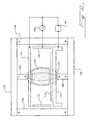
- FIG. 1is an isometric view of a continuous web application of a preferred embodiment.
- a web 10 of flexible materialis disposed around conveyor rolls 11 and 12.
- Web 10can be either two separate materials or one continuous web substrate conveyed from roll 11 to roll 12 with idler rolls not shown.
- Conveyor rolls 11 and 12are constructed of a high permeability material such as carbon steel and are fabricated of sufficient thickness to carry a magnetic field.
- Conveyor rolls 11 and 12are connected to one side of power supply 18 and form one electrode of the electric circuit.
- the power supply 18should be a pulsed DC or AC supply to capacitively couple power though the web substrate if the substrate is a dielectric material.
- the second electrodeis an annular member 13 positioned roughly equidistant from the center of the gap between rolls 11 and 12.
- a magnetic fieldis created across the gap between rolls 11 and 12 with permanent magnets 15 and magnetic shunts 14 and 16.
- the magnetic field strength between rolls 11 and 12must be sufficient to magnetize electrons at least in a portion of the magnetic mirror between the rolls 11 and 12.
- Pole pieces 14are disposed a small distance from rolls 11 and 12 such that the distance is less than the plasma dark space sheath distance.
- Pole pieces 14, magnets 15 and magnet shunt 16are not connected to power supply 18.
- the assemblyis located in a vacuum chamber (not shown). Process gases are supplied into the vicinity of the source at a total pressure of approximately 1-100 mTorr by known techniques. When power supply 18 is turned on, a plasma 17 is struck in the gap between the rolls 11 and 12.
- Approximately 300V - 800Vis required, similar to a magnetron sputter cathode.
- the plasmais magnetically confined in this preferred embodiment to a region between the two roll surfaces covered by the web substrate.
- the advantage of this apparatusis that the plasma is contained proximal to the continuously changing web material and therefore the web receives the bulk of PECVD coating, plasma treatment or other plasma process.
- the capacitance of the first electrode (cathode)does not change because the coating does not accumulate on the conveyor rolls.
- Coating on the second electrode (anodes) and other parts of the apparatusis reduced because they are relatively distant from the plasma.
- conveyor rolls 11 and 12 and electrode 13can be water cooled using known techniques. Though the ion bombardment of the substrate on the rolls is reduced, for typical industrial uses involving extended operation times, water cooling will be required.
- FIG. 2is a section view of the web coating source of FIG. 1 .
- continuous flexible web material 10is disposed around conveyor rolls 11 and 12.
- a magnetic field 19is created across the gap between rolls 11 and 12 by permanent magnets 15, magnetic shunt 16 and pole pieces 14.
- the magnetic fieldmust be strong enough to magnetize the electron population. This means the minimum field strength at the center of the gap where the magnetic field is weakest must exceed 50 gauss. Typically the field strength should exceed 100 gauss. There is no practical top limit. Use of high strength magnets readily produces field strengths in excess of 1000 gauss at the center of the gap. At these higher strengths, ions, to some extent, are also magnetized.
- the Penning discharge type containment implemented herehas the advantage that a surface does not interfere with electron and ion gyro paths within the contained plasma volume. Therefore ions with their larger gyro radii can be contained.
- ceramic ferrite magnetswere used producing field strengths ranging from 300 - 800 gauss in the center of the gap.
- Other means to produce the required magnetic dipole fieldsuch as rare earth magnets, soft ferrite magnets, AlNiCo magnets or electro magnets can be used to produce similar results. Note that the magnetic field widens in the gap between rolls 11 and 12 forming magnetic mirrors at each roll surface.
- Electric fields 21are created between conveyor roll electrodes 11 and 12 and annular electrode 13 by power supply 18. Electric field 21 and 22 potential lines penetrate into the gap between rolls 11 and 12 producing field lines 21 and 22 that cross magnetic field 19 lines. This geometry produces a closed loop Hall current trap 20 normal to the magnetic field. To explain in more detail, an electron near one negatively charged roll electrode surface will attempt to escape along the electric field lines 21 or 22.
- the electric field lines 21 and 22emanate from web surface 10 on rolls 11 and 12 and begin curving away from the gap between the roll surfaces. Toward the center of the gap, electric fields 21 and 22 begin to converge and at the same time cross the magnetic field 19.
- the electronwhile initially able to move away from the cathode surface, becomes trapped in the converging electric fields and now crossing magnetic field toward the center of the gap. It is important to note that not only are the electrons trapped in the plane of this section view, but they are also trapped in the third dimension into and out of the paper. This occurs because electric fields 21 and 22 continue to cross magnetic field 19 completely around magnetic field 19. As the Hall current flows into and out of the paper, this current is confined to region 20 in an endless loop. This produces an efficient electron confinement and a ring of intense plasma 20 between the two roll electrode web surfaces inside the magnetic field 19.
- an intense plasma ring 20is generated.
- the voltage and the frequency requiredwill depend upon the substrate used and process conditions. For example, for the figures depicted, a 50kHz to 460kHz plasma power supply was used. A transformer type matching network with an 8:1 turn ratio was used to increase the voltage at the electrodes. The source rolls were 6" long with the different magnet configurations implemented. Power supply output powers ranged from 100 - 500 watts. Earlier work was done with 3" long rolls and lower powers. From all indications, extending the source has no limitations. Similar to a planar magnetron source, the confined Hall current race track can be extended out to substrate widths of several meters.
- Radio frequencyis also an option (13.56MHz).
- the efficient electron containmentproduces a relatively low impedance plasma allowing frequencies lower than 13.56MHz to be used at low pressures (10mTorr).
- Lower frequency power suppliesare generally lower cost and the total circuit produces less noise. Inside the vacuum chamber, lower frequencies also produce less spurious plasma. Lower frequency systems are also generally safer. Though lower frequencies are suggested, this should not limit the invention to these frequencies. Higher frequency operation will also benefit from the electron containment schemes presented.
- the negative electrodecan be connected to the rolls or to the substrate directly via a sliding brush or other known method.
- the substratethen is definitively the cathode and the positive terminal is connected to anode 13.
- the terms anode and cathodehave less meaning.
- the rolls and surrounding "anode”have been termed electrodes herein to use more general terms related to AC circuits. For the figures depicted, the surrounding electrode 13 is connected to ground.
- the lower power mode where the Hall current ring can be seencorrelates to the collimated mode.
- the diffuse modemay be regarded as the operation mode of the source. In this mode, the electric fields are no longer paths from one electrode to the opposed electrode.
- the plasma cloudbecomes conductive, and the typical abnormal glow plasma potential applies.
- the collimated mode fields and electron motionare described to communicate the underlying operating principle of endless Hall current confinement within a simple dipole magnetic field.
- the inventive methodcan be readily understood as can the extendibility of this method to a myriad of dipole, Penning type configurations.
- the Hall current confinementis still operating, producing a confined, low pressure, low impedance plasma.
- electrode 13does not have to be continuous to create the described Hall current containment electric fields that circumvent the magnetic field.
- a segmented or partial electrodemust only have sufficient presence around the magnetic field to create continuous electric fields. The reason for this is the extreme mobility of electrons once free of the confining magnetic field. For instance, in the source depicted in FIGS. 1 and 2 , if shunt 16 was connected as the only anode electrode opposite rolls 11 and 12, the electric field would still circumvent and penetrate the entire magnetic field per the inventive method. Even in a long, 2 meter source, once outside the constraining magnetic field, electrons would easily find their way to shunt 16.
- FIG. 3shows a section view of the web coating plasma apparatus of FIGS. 1 and 2 inside a vacuum chamber 25.
- a schematic web pathcomprises unwind roll 22, idler rolls 23 and rewind roll 24.
- FIG. 4shows a section view of a web coating apparatus similar to FIGS. 1 and 2 .
- both electrode polesare covered by the web substrate.
- idler rolls 75and possibly web aligning equipment not shown
- deposition on the electrodesis largely eliminated. Since the glow is in contact with only the substrate, material usage is maximized as is power efficiency while maintenance is minimal. Note that by moving anode rolls 73 and 74 closer or farther away from the plasma, plasma contact, contact energies and the overall shape of the plasma can be altered.
- Power supply 77is connected between electrode rolls 71 and 72 and opposite electrode rolls 73 and 74.
- the magnetic field 79is created in the gap with an assembly of permanent magnets and magnetic shunts 78.
- Another alternative connection arrangementis to connect the power supply to idler rolls 75 rather than rolls 73 and 74 making idler rolls 75 serve as the opposite electrode. Then rolls 73 and 74 are left to electrically float. Either of these configurations is useful when an electrically isolating film such as SiOx is deposited by PECVD. By covering the plasma exposed surfaces with the substrate, long runs can be made without the process parameters changing due to buildup on the electrodes.
- FIG. 5shows a section view of another embodiment of a web coating apparatus.
- the substrate supporting electrode rolls 11 and 12are hollow and made of a non-magnetic material such as stainless steel (300 series).
- magnets 120 and roll shaft shunt 121carry the magnetic field from magnets 15 and shunt 16 to create gap field 19. This is different than the earlier depictions that used a permeable material roll. While more complicated, the advantage of internal magnets is the gap field 19 tends to be better defined, and the magnet length can be tailored to the desired web width. For instance, if the rolls are a constant 64 inches wide, the magnets can be 58 inches long for a 60 inch web width.
- Plasmais then concentrated over the roll region covered by web, and the ends of the roll receive less coating.
- Magnetic field shunt 122collects stray field from the region between magnets 15. This helps to further define mirror magnetic field 19 and to contain plasma 17 into the region between roll electrodes 11 and 12.
- Idler rolls 126 and 127route the web from roll 11 to roll 12. Since web 10 "sees" the plasma as the web passes from idler roll 126 to 127, additional treatment, coating, etc. is accomplished.
- an alternating current power supply 18is connected to both rolls as one electrode and to conductive surfaces 124 and 125 as the other. The frequency of the AC must be sufficient to capacitively couple though web 10. For packaging type PET flexible web, the frequency must be above 20kHz.
- Frequencies up to and beyond 13.56MHzmay be used with success although an advantage of the inventive method is that because of the efficient Hall current confinement, lower "mid-frequency" frequencies from 40-500kHz may be used. Power supplies at these lower frequencies tend to radiate less, and load matching can be accomplished with simple transformer type networks. Both 124 and 125 have conductive surfaces not facing the plasma. This helps to keep a portion of the electrodes conductive when an insulating coating is deposited.
- Another feature of the inventive methodis the use of a magnetic mirror field 19 between substrate supporting rolls 11 and 12.
- a mirror fieldis produced when the magnetic field strength at the surface of the substrate 10 is greater than the field in the center of the gap.
- the effect of a mirror field on electronsis to push the electrons into the center of the gap, away from the region of stronger field.
- Electronsthen are constrained in three axes by the magnetic field. They are constrained from moving across magnetic field lines, and they are constrained from moving toward the roll surfaces. The result is the plasma 17 tends to be focused into the center of the gap. This has several advantages. The further constraining of electrons produces a higher plasma "pressure" in the central plasma region as ions electro-statically are focused into the center following the electrons.
- the conveyor rolls 11 and 12can be moved closer together or farther apart to different effect. As the rolls are moved closer together, the electric fields have a harder time penetrating into the center of the gap.
- the Hall current ring 20remains visible at higher powers, and the virtual cathode created in the center of the gap results in an ion flow into the center of the gap. Continuing to move the rolls closer together eventually extinguishes all signs of plasma in the center of the gap. If the rolls are moved too close together, the Hall current cannot move from one side of the rolls to the other, and the plasma is extinguished. This can be solved by configuring the magnets to allow the plasma to circle around the outside ends of the rolls, or the rolls can be sloped at each end to open the gap at the ends.
- the best gap between the rollsis approximately 1.25 to 2 inches given the arrangement shown in FIG. 5 with Ceramic 8 type magnets. This is small enough to maintain a strong magnetic field between the rolls while large enough to allow the Hall current to pass between the rolls at the ends. Larger rolls with more magnets or the use of rare earth magnets would allow the gap to be larger than 2 inches.
- FIG. 6is an isometric view of the continuous web application shown in FIG. 5 .
- FIG. 7shows a section view of another flexible web source. This source hides the A electrodes 130 and 134 behind web 76 to reduce the coating received by these electrodes. Electrode 130 also serves as the magnet shunt bringing magnetic field from roll 71 and magnet 131 to roll 72 and magnet 131. Electrode 130 and shunts 132 are made of a high permeability material. Electrode 134 can also be made of a high permeability material without effecting operation.
- FIG. 8is a section view of a device employing an alternative embodiment.
- electrode surfaces 1 and 2are hollow conveyor rolls and face each other across a gap.
- a magnetic field 13is formed outside the rolls in the shape of a closed loop racetrack with magnet sets 6 and 9. Rather than externally returning the magnetic field, the return magnetic field 14 is formed inside magnetic field 13 with magnets 7 and 10. Magnetic shunts 4 and 5 complete the magnetic circuit.
- the magnet assembliesdo not turn with the conveyor rolls but remain fixed facing each other.
- a flexible web substrate 3is disposed around conveyor rolls 1 and 2.
- the electrical circuitis formed with conveyor rolls 1 and 2 connected in parallel to power supply 18 and electrode 12 with plasma 16 completing the electrical circuit.
- Electrode 12substantially circumvents the magnetic field 13 thereby creating electric fields 15 and 19 from conveyor rolls 1 and 2 surfaces to anode 12.
- An alternating or pulsed DC voltageis generated by power supply 18 to couple the field through web substrate 3.
- Electric fields 15 and 19are parallel to the magnetic field at the substrate 3 surface and gradually become more normal to magnetic field 13 toward the center plane between the rolls 1 and 2.
- These diverging fields, in conjunction with magnetic field 13,form a closed loop Hall current trap 16 in magnetic field 13.
- An intense plasmaforms in the Hall current trap 16. Note that the electric fields 15 and 19 do not penetrate fully into the gap between rolls 1 and 2. This creates a virtual cathode in this gap.
- a process gas or combination of gasesis presented to the vicinity of the conveyor rolls using known techniques for total pressures ranging from 0,133 to 13,3 Pa (from 1 to 100mTorr).
- Power supply 18is turned on, and the plasma 16 lights.
- the electrode 12does not necessarily have to be continuous to create Hall current containment electric fields 15 and 19 circumventing the magnetic field 13. The important thing is to have sufficient electrode 12 presence around the magnetic field to create the continuous confinement electric fields 15 and 19.
- this electrode 12can be removed and the chamber wall used as the electrode. While electrode 12 as shown will operate as described, it is an additional part and it can become coated in a PECVD operation. It is shown in FIG. 7 to assist the reader. All advantages of the preferred embodiment are maintained by using the chamber wall as the electrode 12 with the exception of the ability to direct the resulting ion current into the gap between rolls 1 and 2. As stated above, as long as electric fields 15 and 19 circumvent magnetic field 13, the electrode 12 can take a variety of forms.
- the Hall currentis contained between the two roll electrodes 1 and 2.
- the substrateis made the target in a magnetron sputtering configuration. This results in intense ion bombardment of the substrate with the attendant high temperature load and ion ablation effects.
- the inventive methodcontains the intense Hall current away from the surface of the substrate. While a bright plasma is formed, the ion bombardment of the substrate is reduced. This results in a lower substrate temperature allowing a wider range of substrate materials to be used along with slower conveyor speeds. Slower process speeds allow thicker coatings to be deposited. Also, ablation of the substrate is reduced.
- FIG. 9an isometric view of the web embodiment of FIG. 8 is depicted with the chamber wall and idler rolls 20 and 21 acting as grounded electrodes.
- Conveyor rolls 1 and 2are shown with web 3 disposed around the rollers.
- the web 3is a continuous web with idler rolls 20 and 21 serving to convey the web between rolls 1 and 2.
- the plasma ring 16is created by the inventive method between rollers 1 and 2. Note that the plasma is in close proximal contact with continuously moving web 3 while other surfaces are substantially more distant. This is a major advance in coating, etching or plasma treating web substrates. Where in the prior art, the electrodes often receive the bulk of the coating, the system of Figures 8 and 9 dramatically improves this situation.
- the device and methodcan be scaled to any width required. Also, uniformity of the plasma is consistent with that achievable with magnetron sputtering. This far exceeds uniformities possible with non-magnetically enhanced RF diode discharges over wide substrates. For continuous operation in production, rolls 1 and 2 are water cooled using known techniques.
- FIG. 10shows another embodiment of the inventive method.
- rolls 1 and 2are moved apart to create both closed magnetic tunnels 25 and 26 over rolls 1 and 2 and crossing magnetic fields 13 and 14.
- the magnetic tunnels 25 and 26are similar to the magnetic confinement of a magnetron cathode.
- process gasis supplied and power supply 18 is energized, plasma lights in the containment rings 16, 27 and 28.
- This effectcan be adjusted by the magnetic field strength, distance between the rolls, magnet configuration, process gases and power supply settings.
- one cathodecould be a planar magnetron. In this way, a flexible web could receive a sputter coating while also being bombarded by plasma species due to containment rings 16 and 27.
- FIG. 11shows another preferred embodiment, this one has the magnetic containment outside of the rolls.
- Idler rolls 160, 161 and 162transport web substrate 10 in a path across the faces of pole pieces 14. Note that the web does not touch poles 14 but rather moves adjacent to it. The idea is to keep the web close enough to the poles 14 that plasma does not form between poles 14 and the web.
- at least one surface of the substrateis positioned between the plasma and the plasma facing surface supporting the substrate.
- the back side of the webis between the plasma and the electrode surface. There is naturally a region without plasma near the electrode that is termed the "dark space". This is shown in this figure as excluded from the shaded plasma region 17.
- the dark spaceis a well known phenomenon. Magnets 15 produce magnetic field 19 in the gap between pole pieces 14.
- a power supply(not shown) is connected to poles 14 as one electrode and electrode 13. This produces the required electric fields inside the magnetic field and contained plasma region 17.
- the process gascan be distributed to improve gas utilization and enhance process uniformity. Gas distribution tube 163 is shown attached to electrode 13. In this location, the process gas is forced to flow through the plasma on its way to the vacuum pump through the gaps in the lower electrode 13. End shield plates are not shown that prevent the gas from leaving the ends of the source. Depending upon the process type, this can lead to more efficient use of the process gasses.
- FIG. 12shows a rigid substrate source implementing the inventive method.
- a silicon wafer 170is placed on platen 171.
- Bar magnet 180is placed under platen 171 and extends under the wafer.
- a magnetic field 179is created between the wafer surface and surface 177 with a second bar magnet 182, shunt 172, shunt 176 and magnets 174.
- Electrode 177is a non-magnetic material such as copper or titanium. Electrode 177 can be fitted with a plasma facing surface that either enhances or is benign to the process. This can be important as sputtering of surface 177 does occur.
- Electrodes 173are constructed of a high permeability material to capture stray magnetic field.
- Power supply 178is connected to platen 171 and electrode 172 and to electrode 173 as shown.
- 181is a device to control current or voltage at the wafer surface and can be inserted if needed.
- the resulting magnetic and electric fieldsresult in the contained Hall current of the inventive method and produces a dense plasma 175 in the gap between wafer 170 and electrode 177.
- Shunts 176 and 172 and magnets 180 and 182are rotated to uniformly plasma treat the wafer.
- magnets 180 and 182could be smaller bar magnets and could be moved in a pattern to move the plasma over the wafer surface as required.
- a means for detecting the completion of the process stepcould be used to determine when all areas of the wafer had received adequate treatment.
- the substrateis positioned over only one electrode in FIG. 12 .
- This same approachcan be implemented in the web based apparatus shown above.
- one rollcould support the web substrate while the opposite electrode could be a planar sputter target.
- Many embodimentswill be apparent to one skilled in the art.
- the inventive methodpresents a fundamentally novel plasma source using a modified Penning discharge with a continuously moving substrate (moving in relation to the plasma). As the important features of a highly effective electron containment bottle and the closed drift containment nature of the source are understood, many embodiments of the fundamental source will be evident.
- the magnetic and electric field arrangementsimilar to a Penning discharge, effectively traps the electron Hall current in a region between two surfaces.
- a substrateis positioned proximal to at least one of the electrodes and is moved relative to the plasma, the substrate is plasma treated, coated or otherwise modified depending upon the process gas used and the process pressure.
- This confinement arrangementproduces dramatic results not resembling known prior art.
- many applications for PECVD, plasma etching, plasma treating, sputtering or other plasma processeswill be substantial improved or made possible.
- applications using flexible websare benefited.
- a summary of the web application benefitsare:
Landscapes
- Chemical & Material Sciences (AREA)
- Engineering & Computer Science (AREA)
- Physics & Mathematics (AREA)
- Plasma & Fusion (AREA)
- Mechanical Engineering (AREA)
- Analytical Chemistry (AREA)
- Organic Chemistry (AREA)
- Metallurgy (AREA)
- General Chemical & Material Sciences (AREA)
- Chemical Kinetics & Catalysis (AREA)
- Materials Engineering (AREA)
- Optics & Photonics (AREA)
- Combustion & Propulsion (AREA)
- Spectroscopy & Molecular Physics (AREA)
- Plasma Technology (AREA)
- Chemical Vapour Deposition (AREA)
- Physical Vapour Deposition (AREA)
- ing And Chemical Polishing (AREA)
- Drying Of Semiconductors (AREA)
- Analysing Materials By The Use Of Radiation (AREA)
- Carbon And Carbon Compounds (AREA)
Abstract
Description
- The present invention relates to a Penning discharge plasma source. Before turning to the detailed description of the presently preferred embodiments, related prior art is discussed below. The related prior art is grouped into the following sections: magnetic confinement and the Penning cell source, facing target sputtering, and plasma treatment with a web on a drum. Other prior art methods and apparatuses are also discussed.
U.S. Patent No. 2,146,025 to Penning discloses the first use of magnetic fields to enhance and confine a plasma for sputtering. The devices shown in Penning form the foundation for much of the future magnetically enhanced plasma source work. In several configurations shown, a magnetic field is used to extend the path length of electrons as they travel from the cathode to the anode. In extending the path length, the likelihood of a collision with a neutral atom and the creation of an ion and an additional electron increases. Penning uses this effect to achieve high rate sputtering of a cathode surface (or cathode erosion as he describes it). The source inFigures 5 and6 in Penning is termed a Penning Cell or a Penning Discharge. Versions of this have been used to make ion beam sources, getter vacuum pumps, and other sources. In the figures, the magnetic field is a solenoid type field, stronger in the center of the gap than at the two cathode surfaces.- Magnetically confined plasmas are also discussed inJ. Reece Roth, Industrial Plasma Engineering, Volume 1: Principles, IOP Publishing, Ltd. 1995. Section 9.5.5 pp 334-337 of this reference presents several Penning discharge configurations. One configuration, termed a Modified Penning Discharge, uses a mirror magnetic field to further improve the containment of electrons and ions. In Roth's work, sufficient magnetic field strength is used to contain ions as well as electrons.
- The following patents and reference disclose a method and apparatus implementing a sputtering technique where two cathodes face each other and a magnetic field is created normal to the surface of the cathodes:
4,407,894 ;4,576,700 ;4,767,516 ;4,784,739 ;4,842,708 ;4,963,524 ;5,000,834 ;5,135,819 ;5,328,583 ;6,156,172 ; andMusil et al., Unbalanced magnetrons and new sputtering systems with enhanced plasma ionization, American Vacuum Society, Journal of Vacuum Science and Technology A 9 (3) May/June 1991. In most of these documents, the substrate is placed outside of the gap between the cathode surfaces. For example,U.S. Patent No. 4,767,516 to Nakatsuka et al. shows facing target sources used to coat web. The substrate is parallel to the magnetic field axis and outside the plasma region. U.S. Patent No. 4,963,524 to Yamazaki shows a method of producing superconducting material. An opposed target arrangement is used with the substrate positioned between the electrodes in the magnetic field. The difference is that the substrates shown here are in the middle of the gap. Testing shows this does not work well. The Hall current generated within the magnetic field tends to be distorted and broken when substrates are placed where shown in this patent. When this happens, the plasma is extinguished and/or the voltage is much higher.- In the article by Musii et al., several plasma sources are reviewed. Two figures,
FIGS. 1e and f , show opposed target arrangements. In the text, it describes either placing substrates out of the plasma or close to the plasma depending upon the level of bombardment desired. - In
U.S. Patent Nos. 5,224,441 and5,364,665 to Felts et al. , a flexible substrate is disposed around an electrified drum with magnetic field means opposite the drum behind grounded shielding. In this arrangement, the shield opposite the drum is either grounded or floating. The magnet and electrode configuration also does not lend itself to effectively contain electron Hall currents. Note that in this patent, as the shield surface is coated, the overall system capacitance decreases, changing the circuit impedance. Shield coating is also a maintenance problem in a production operation. To exemplify the scale of the potential shield coating, if a 90 cm diameter roll of 12 um polymer film (approximately 50,000 meters of film) is coated with a 30 nanometer thick coating, assuming the shield opposite the substrate receives an equal amount of coating, then the shield will collect a >2mm thick polymer coating by the end of the run. - In
U.S. Patent No. 6,110,540 to Countrywood et al. , a disclosure is made regarding the electrified drum technology referenced above. The problem of electrode coating is acknowledged in this patent. A method to maintain the conductivity of the non-drum electrode is disclosed. One issue with this solution is that, since polymerization occurs wherever there is glow, the glow at the gas feed electrode will be a high rate polymerization site causing additional maintenance headaches. - The problem of coating non-substrate surfaces is addressed in
U.S. Patent No. 4,863,756 to Hartig et al. In this disclosure, the substrate is continuously moved over a sputter magnetron surface with the surface facing the magnetron located inside the dark space region of the cathode. In this way, the magnetic field of the magnetron passes through the substrate and is closed over the substrate surface constricting the plasma onto the surface. The problem with this method is the substrate on the magnetron effectively becomes a sputtering target and receives intense ion bombardment. Therefore, while a PECVD film is being deposited on the substrate, the intense ion bombardment is simultaneously ablating the film. Another difficulty is that due to the intense ion bombardment, the substrate can become very hot. This limits substrate materials options and requires the substrate move at a speed sufficient to prevent damage from overheating. This limits the application options for this device. U.S. Patent No. 4,761,219 to Sasaki et al. shows a magnetic field passing through a gap with the wafer on one electrode surface. In this case, the electrodes are opposed to each other.U.S. Patent No. 5,099,790 to Kawakami shows a microwave source with a moving magnet below the wafer to even out the coating on the wafer. In another figure, the substrates are moved over a stationary magnet(s). This source does not have opposed cathode (electrode) surfaces.- The present invention is defined by the following claims, and nothing in this section should be taken as a limitation on those claims.
- By way of introduction, the preferred embodiments described below relate to a Penning discharge plasma source. In one preferred embodiment, a plasma treatment apparatus is provided comprising: at least two surfaces with a gap between the surfaces, wherein both surfaces are connected as electrodes; at least one magnetic field extending between the surfaces through the gap; at least one anode structure disposed around the at least one magnetic field creating diverging electric fields inside the at least one magnetic field to form a closed loop Hall current containment region within the at least one magnetic field, where upon with sufficient gas pressure and voltage between the electrodes and the anode structure, a plasma is formed in the containment region; and at least one continuously moving substrate positioned to be treated by the plasma, wherein the at least one continuously moving substrate is supported on at least one plasma facing surface and wherein at least one surface of the at least one continuously moving substrate is positioned between the plasma and the at least one plasma facing surface.
- Other preferred embodiments are provided, and each of the preferred embodiments can be used alone or in combination with one another. The preferred embodiments will now be described with reference to the attached drawings.
FIG. 1 shows an isometric view of a flexible web apparatus of a preferred embodiment.FIG. 2 shows a section view of the web apparatus ofFIG. 1 with magnetic and electric field lines illustrated.FIG. 3 shows the web apparatus ofFIG. 1 inside a vacuum chamber.FIG. 4 shows a section view of a web apparatus wherein both cathode and anode electrodes are covered by the substrate.FIG. 5 shows a section view of a flexible web apparatus employing a thin sheet metal shunt to collect stray magnetic field.FIG. 6 shows an isometric view of theFIG. 5 source.FIG. 7 shows a section view of another preferred embodiment with the flexible web covering the opposite electrode.FIG. 8 shows a section view of a rotating roll source where the return magnetic field is brought through the center of the rolls instead of externally via a shunt and magnets.FIG. 9 is an isometric view of theFIG. 8 source.FIG. 10 is a section view depicting a variation on theFIG. 8 source.FIG. 11 is a section view of another flexible web source.FIG. 12 is a section view of a rigid substrate (wafer) plasma source of a preferred embodiment.FIG. 1 is an isometric view of a continuous web application of a preferred embodiment. Aweb 10 of flexible material is disposed around conveyor rolls 11 and 12.Web 10 can be either two separate materials or one continuous web substrate conveyed fromroll 11 to roll 12 with idler rolls not shown. Conveyor rolls 11 and 12 are constructed of a high permeability material such as carbon steel and are fabricated of sufficient thickness to carry a magnetic field. Conveyor rolls 11 and 12 are connected to one side ofpower supply 18 and form one electrode of the electric circuit. Thepower supply 18 should be a pulsed DC or AC supply to capacitively couple power though the web substrate if the substrate is a dielectric material. The second electrode is anannular member 13 positioned roughly equidistant from the center of the gap betweenrolls rolls permanent magnets 15 andmagnetic shunts rolls rolls Pole pieces 14 are disposed a small distance fromrolls Pole pieces 14,magnets 15 andmagnet shunt 16 are not connected topower supply 18. The assembly is located in a vacuum chamber (not shown). Process gases are supplied into the vicinity of the source at a total pressure of approximately 1-100 mTorr by known techniques. Whenpower supply 18 is turned on, aplasma 17 is struck in the gap between therolls electrode 13 can be water cooled using known techniques. Though the ion bombardment of the substrate on the rolls is reduced, for typical industrial uses involving extended operation times, water cooling will be required.FIG. 2 is a section view of the web coating source ofFIG. 1 . As described inFIG. 1 , continuousflexible web material 10 is disposed around conveyor rolls 11 and 12. Amagnetic field 19 is created across the gap betweenrolls permanent magnets 15,magnetic shunt 16 andpole pieces 14. As stated above, the magnetic field must be strong enough to magnetize the electron population. This means the minimum field strength at the center of the gap where the magnetic field is weakest must exceed 50 gauss. Typically the field strength should exceed 100 gauss. There is no practical top limit. Use of high strength magnets readily produces field strengths in excess of 1000 gauss at the center of the gap. At these higher strengths, ions, to some extent, are also magnetized. The Penning discharge type containment implemented here has the advantage that a surface does not interfere with electron and ion gyro paths within the contained plasma volume. Therefore ions with their larger gyro radii can be contained. In all the figures in this application, ceramic ferrite magnets were used producing field strengths ranging from 300 - 800 gauss in the center of the gap. Other means to produce the required magnetic dipole field such as rare earth magnets, soft ferrite magnets, AlNiCo magnets or electro magnets can be used to produce similar results. Note that the magnetic field widens in the gap betweenrolls Electric fields 21 are created betweenconveyor roll electrodes annular electrode 13 bypower supply 18.Electric field rolls field lines magnetic field 19 lines. This geometry produces a closed loop Hallcurrent trap 20 normal to the magnetic field. To explain in more detail, an electron near one negatively charged roll electrode surface will attempt to escape along theelectric field lines electric field lines web surface 10 onrolls electric fields magnetic field 19. The electron, while initially able to move away from the cathode surface, becomes trapped in the converging electric fields and now crossing magnetic field toward the center of the gap. It is important to note that not only are the electrons trapped in the plane of this section view, but they are also trapped in the third dimension into and out of the paper. This occurs becauseelectric fields magnetic field 19 completely aroundmagnetic field 19. As the Hall current flows into and out of the paper, this current is confined toregion 20 in an endless loop. This produces an efficient electron confinement and a ring ofintense plasma 20 between the two roll electrode web surfaces inside themagnetic field 19.- Once this fundamental method of electron containment within a dipole magnetic field is understood, many different configurations are possible that result in several important beneficial outcomes. Two of these benefits are that a uniform plasma is created over wide substrate widths and that ion bombardment of the web is reduced compared to sources where the substrate forms the target in a magnetron sputter arrangement, such as the one disclosed in
U.S. Patent No. 4,863,756 to Hartig et al. Lower ion bombardment rates reduce substrate heating and ablation. More benefits are described throughout this application. - As stated above, when voltage is applied between roll surfaces 11 and 12 covered by
web 10 andelectrode structure 13, anintense plasma ring 20 is generated. The voltage and the frequency required will depend upon the substrate used and process conditions. For example, for the figures depicted, a 50kHz to 460kHz plasma power supply was used. A transformer type matching network with an 8:1 turn ratio was used to increase the voltage at the electrodes. The source rolls were 6" long with the different magnet configurations implemented. Power supply output powers ranged from 100 - 500 watts. Earlier work was done with 3" long rolls and lower powers. From all indications, extending the source has no limitations. Similar to a planar magnetron source, the confined Hall current race track can be extended out to substrate widths of several meters. Note that with conducting substrates such as metal sheet, DC power can be used. Radio frequency is also an option (13.56MHz). Part of the advantage of the invention is that the efficient electron containment produces a relatively low impedance plasma allowing frequencies lower than 13.56MHz to be used at low pressures (10mTorr). Lower frequency power supplies are generally lower cost and the total circuit produces less noise. Inside the vacuum chamber, lower frequencies also produce less spurious plasma. Lower frequency systems are also generally safer. Though lower frequencies are suggested, this should not limit the invention to these frequencies. Higher frequency operation will also benefit from the electron containment schemes presented. - If a DC source is used with a
conductive substrate 10 supported by electrode rolls 11 and 12, the negative electrode can be connected to the rolls or to the substrate directly via a sliding brush or other known method. The substrate then is definitively the cathode and the positive terminal is connected toanode 13. Using AC or RF, the terms anode and cathode have less meaning. The rolls and surrounding "anode" have been termed electrodes herein to use more general terms related to AC circuits. For the figures depicted, the surroundingelectrode 13 is connected to ground. - As the power is raised to the source, the plasma expands beyond
ring 20 and fills the region between the roll surfaces withplasma cloud 17. In terms of ion sources, the lower power mode where the Hall current ring can be seen correlates to the collimated mode. As the power is raised, with the pressure in the mTorr range (1-100mTorr), the contained plasma volume shifts into the diffuse mode. The diffuse mode may be regarded as the operation mode of the source. In this mode, the electric fields are no longer paths from one electrode to the opposed electrode. The plasma cloud becomes conductive, and the typical abnormal glow plasma potential applies. The collimated mode fields and electron motion are described to communicate the underlying operating principle of endless Hall current confinement within a simple dipole magnetic field. When one of the sources depicted is operated in the lower power collimated mode and the Hall current ring is clearly visible, the inventive method can be readily understood as can the extendibility of this method to a myriad of dipole, Penning type configurations. In the diffuse mode, while not visible, the Hall current confinement is still operating, producing a confined, low pressure, low impedance plasma. - Note that
electrode 13 does not have to be continuous to create the described Hall current containment electric fields that circumvent the magnetic field. A segmented or partial electrode must only have sufficient presence around the magnetic field to create continuous electric fields. The reason for this is the extreme mobility of electrons once free of the confining magnetic field. For instance, in the source depicted inFIGS. 1 and2 , ifshunt 16 was connected as the only anode electrode opposite rolls 11 and 12, the electric field would still circumvent and penetrate the entire magnetic field per the inventive method. Even in a long, 2 meter source, once outside the constraining magnetic field, electrons would easily find their way to shunt 16. FIG. 3 shows a section view of the web coating plasma apparatus ofFIGS. 1 and2 inside avacuum chamber 25. A schematic web path comprises unwindroll 22, idler rolls 23 and rewind roll 24.FIG. 4 shows a section view of a web coating apparatus similar toFIGS. 1 and2 . In this embodiment, both electrode poles are covered by the web substrate. Using this electrode arrangement along with idler rolls 75 (and possibly web aligning equipment not shown), deposition on the electrodes is largely eliminated. Since the glow is in contact with only the substrate, material usage is maximized as is power efficiency while maintenance is minimal. Note that by moving anode rolls 73 and 74 closer or farther away from the plasma, plasma contact, contact energies and the overall shape of the plasma can be altered.Power supply 77 is connected between electrode rolls 71 and 72 and opposite electrode rolls 73 and 74. Themagnetic field 79 is created in the gap with an assembly of permanent magnets andmagnetic shunts 78. Another alternative connection arrangement is to connect the power supply to idler rolls 75 rather thanrolls idler rolls 75 serve as the opposite electrode. Then rolls 73 and 74 are left to electrically float. Either of these configurations is useful when an electrically isolating film such as SiOx is deposited by PECVD. By covering the plasma exposed surfaces with the substrate, long runs can be made without the process parameters changing due to buildup on the electrodes.FIG. 5 shows a section view of another embodiment of a web coating apparatus. In this embodiment, the substrate supporting electrode rolls 11 and 12 are hollow and made of a non-magnetic material such as stainless steel (300 series). Internal to rolls 11 and 12,magnets 120 and rollshaft shunt 121 carry the magnetic field frommagnets 15 and shunt 16 to creategap field 19. This is different than the earlier depictions that used a permeable material roll. While more complicated, the advantage of internal magnets is thegap field 19 tends to be better defined, and the magnet length can be tailored to the desired web width. For instance, if the rolls are a constant 64 inches wide, the magnets can be 58 inches long for a 60 inch web width. Plasma is then concentrated over the roll region covered by web, and the ends of the roll receive less coating.Magnetic field shunt 122 collects stray field from the region betweenmagnets 15. This helps to further define mirrormagnetic field 19 and to containplasma 17 into the region betweenroll electrodes roll 11 to roll 12. Sinceweb 10 "sees" the plasma as the web passes fromidler roll 126 to 127, additional treatment, coating, etc. is accomplished. In this apparatus, an alternatingcurrent power supply 18 is connected to both rolls as one electrode and toconductive surfaces web 10. For packaging type PET flexible web, the frequency must be above 20kHz. Frequencies up to and beyond 13.56MHz may be used with success although an advantage of the inventive method is that because of the efficient Hall current confinement, lower "mid-frequency" frequencies from 40-500kHz may be used. Power supplies at these lower frequencies tend to radiate less, and load matching can be accomplished with simple transformer type networks. Both 124 and 125 have conductive surfaces not facing the plasma. This helps to keep a portion of the electrodes conductive when an insulating coating is deposited.- Another feature of the inventive method is the use of a
magnetic mirror field 19 betweensubstrate supporting rolls substrate 10 is greater than the field in the center of the gap. The effect of a mirror field on electrons is to push the electrons into the center of the gap, away from the region of stronger field. Electrons then are constrained in three axes by the magnetic field. They are constrained from moving across magnetic field lines, and they are constrained from moving toward the roll surfaces. The result is theplasma 17 tends to be focused into the center of the gap. This has several advantages. The further constraining of electrons produces a higher plasma "pressure" in the central plasma region as ions electro-statically are focused into the center following the electrons. Fewer ions at the surface of the substrate produce less ion bombardment of the substrate. This lowers the substrate temperature and reduces ablation of the surface. Reducing the temperature of the plasma process for a given power input has many advantages. These are detailed at the end of the detailed description section. - Note also that the conveyor rolls 11 and 12 can be moved closer together or farther apart to different effect. As the rolls are moved closer together, the electric fields have a harder time penetrating into the center of the gap. The Hall
current ring 20 remains visible at higher powers, and the virtual cathode created in the center of the gap results in an ion flow into the center of the gap. Continuing to move the rolls closer together eventually extinguishes all signs of plasma in the center of the gap. If the rolls are moved too close together, the Hall current cannot move from one side of the rolls to the other, and the plasma is extinguished. This can be solved by configuring the magnets to allow the plasma to circle around the outside ends of the rolls, or the rolls can be sloped at each end to open the gap at the ends. While these variations are included within the inventive method, they are not recommended as they are more expensive or involve added complexity. The best gap between the rolls is approximately 1.25 to 2 inches given the arrangement shown inFIG. 5 with Ceramic 8 type magnets. This is small enough to maintain a strong magnetic field between the rolls while large enough to allow the Hall current to pass between the rolls at the ends. Larger rolls with more magnets or the use of rare earth magnets would allow the gap to be larger than 2 inches. FIG. 6 is an isometric view of the continuous web application shown inFIG. 5 . Note thehigh permeability shunt 122 extending from primarymagnetic field path rolls electrodes rolls FIG. 7 shows a section view of another flexible web source. This source hides theA electrodes 130 and 134 behindweb 76 to reduce the coating received by these electrodes.Electrode 130 also serves as the magnet shunt bringing magnetic field fromroll 71 andmagnet 131 to roll 72 andmagnet 131.Electrode 130 andshunts 132 are made of a high permeability material. Electrode 134 can also be made of a high permeability material without effecting operation.FIG. 8 is a section view of a device employing an alternative embodiment. In this embodiment, electrode surfaces 1 and 2 are hollow conveyor rolls and face each other across a gap. Amagnetic field 13 is formed outside the rolls in the shape of a closed loop racetrack with magnet sets 6 and 9. Rather than externally returning the magnetic field, the returnmagnetic field 14 is formed insidemagnetic field 13 withmagnets Magnetic shunts 4 and 5 complete the magnetic circuit. The magnet assemblies do not turn with the conveyor rolls but remain fixed facing each other. A flexible web substrate 3 is disposed around conveyor rolls 1 and 2. The electrical circuit is formed with conveyor rolls 1 and 2 connected in parallel topower supply 18 andelectrode 12 withplasma 16 completing the electrical circuit.Electrode 12 substantially circumvents themagnetic field 13 thereby creatingelectric fields anode 12. An alternating or pulsed DC voltage is generated bypower supply 18 to couple the field through web substrate 3.Electric fields magnetic field 13 toward the center plane between therolls magnetic field 13, form a closed loop Hallcurrent trap 16 inmagnetic field 13. An intense plasma forms in the Hallcurrent trap 16. Note that theelectric fields rolls magnetic field 14 in the center of the gap betweenrolls lines 17 inFIG. 8 .- In operation, a process gas or combination of gases is presented to the vicinity of the conveyor rolls using known techniques for total pressures ranging from 0,133 to 13,3 Pa (from 1 to 100mTorr).
Power supply 18 is turned on, and theplasma 16 lights. - Note that the
electrode 12 does not necessarily have to be continuous to create Hall current containmentelectric fields magnetic field 13. The important thing is to havesufficient electrode 12 presence around the magnetic field to create the continuous confinementelectric fields - Additionally in regard to the
electrode 12, thiselectrode 12 can be removed and the chamber wall used as the electrode. Whileelectrode 12 as shown will operate as described, it is an additional part and it can become coated in a PECVD operation. It is shown inFIG. 7 to assist the reader. All advantages of the preferred embodiment are maintained by using the chamber wall as theelectrode 12 with the exception of the ability to direct the resulting ion current into the gap betweenrolls electric fields magnetic field 13, theelectrode 12 can take a variety of forms. - While this embodiment has the advantage of no external magnets or shunts, the rolls must be positioned carefully with respect to each other to achieve the magnetic fields as shown. If the rolls are too far apart, the magnetic fields change to more closely approximate two facing magnetron sources (similar to two sources per
U.S. Patent No. 4,863,756 to Hartig et al. ). If the rolls are too close together, the Hall current cannot pass through the gap between the rolls at the turnarounds at each end. As discussed earlier, alternatives are available such as allowing the Hall current to pass beyond the end of the rolls and turnaround outside the gap or the rolls may be tapered at the ends to open the gap at the turnarounds. At any rate, one should be aware of these limitations when building a source of this type. - An important aspect of the invention that differs from prior art is that the Hall current is contained between the two
roll electrodes - In
FIG. 9 , an isometric view of the web embodiment ofFIG. 8 is depicted with the chamber wall and idler rolls 20 and 21 acting as grounded electrodes. Conveyor rolls 1 and 2 are shown with web 3 disposed around the rollers. The web 3 is a continuous web with idler rolls 20 and 21 serving to convey the web betweenrolls plasma ring 16 is created by the inventive method betweenrollers Figures 8 and9 dramatically improves this situation. Other advantages evident in this figure are that the device and method can be scaled to any width required. Also, uniformity of the plasma is consistent with that achievable with magnetron sputtering. This far exceeds uniformities possible with non-magnetically enhanced RF diode discharges over wide substrates. For continuous operation in production, rolls 1 and 2 are water cooled using known techniques. FIG. 10 . shows another embodiment of the inventive method. In this apparatus, rolls 1 and 2 are moved apart to create both closedmagnetic tunnels rolls magnetic fields magnetic tunnels power supply 18 is energized, plasma lights in the containment rings 16, 27 and 28. This effect can be adjusted by the magnetic field strength, distance between the rolls, magnet configuration, process gases and power supply settings. Many variations are possible. For instance, instead of two rolls, one cathode could be a planar magnetron. In this way, a flexible web could receive a sputter coating while also being bombarded by plasma species due to containment rings 16 and 27.FIG. 11 . shows another preferred embodiment, this one has the magnetic containment outside of the rolls. Idler rolls 160, 161 and 162transport web substrate 10 in a path across the faces ofpole pieces 14. Note that the web does not touchpoles 14 but rather moves adjacent to it. The idea is to keep the web close enough to thepoles 14 that plasma does not form betweenpoles 14 and the web. In some of the following claims, it is stated that at least one surface of the substrate is positioned between the plasma and the plasma facing surface supporting the substrate. For example, in the embodiment described above, the back side of the web is between the plasma and the electrode surface. There is naturally a region without plasma near the electrode that is termed the "dark space". This is shown in this figure as excluded from the shadedplasma region 17. The dark space is a well known phenomenon.Magnets 15 producemagnetic field 19 in the gap betweenpole pieces 14. A power supply (not shown) is connected topoles 14 as one electrode andelectrode 13. This produces the required electric fields inside the magnetic field and containedplasma region 17. Of additional note in this figure is that there is no magnet or permeable material return path for the magnetic circuit. The return path is helpful because it allows the field in the gap to be stronger and reduces spurious closed field plasma regions. While advantageous, this figure shows that it is not required for the inventive method. The process gas can be distributed to improve gas utilization and enhance process uniformity.Gas distribution tube 163 is shown attached toelectrode 13. In this location, the process gas is forced to flow through the plasma on its way to the vacuum pump through the gaps in thelower electrode 13. End shield plates are not shown that prevent the gas from leaving the ends of the source. Depending upon the process type, this can lead to more efficient use of the process gasses.- All the sources shown have been adapted for flexible web type substrates. This has been done because of the commercial value of an improved web coating source and because of the requirement that the substrate become an electrode in the electric circuit. For the substrate to become an electrode in the case of an insulating substrate, the substrate must be thin enough to capactively pass electrical current. Web substrates are typically thin enough to readily pass AC current even in the 10's of kHz. As thicker substrates are used, the AC frequency must rise up eventually to RF at 13.56 MHz. While as described above, RF 13.56 MHz presents additional challenges, it can be used in all the sources presented.
FIG. 12 shows a rigid substrate source implementing the inventive method. Asilicon wafer 170 is placed onplaten 171.Bar magnet 180 is placed underplaten 171 and extends under the wafer. Amagnetic field 179 is created between the wafer surface andsurface 177 with asecond bar magnet 182,shunt 172,shunt 176 andmagnets 174.Electrode 177 is a non-magnetic material such as copper or titanium.Electrode 177 can be fitted with a plasma facing surface that either enhances or is benign to the process. This can be important as sputtering ofsurface 177 does occur.Electrodes 173 are constructed of a high permeability material to capture stray magnetic field.Power supply 178 is connected to platen 171 andelectrode 172 and to electrode 173 as shown. 181 is a device to control current or voltage at the wafer surface and can be inserted if needed. The resulting magnetic and electric fields result in the contained Hall current of the inventive method and produces adense plasma 175 in the gap betweenwafer 170 andelectrode 177.Shunts magnets magnets - Note that the substrate is positioned over only one electrode in
FIG. 12 . This same approach can be implemented in the web based apparatus shown above. For instance, one roll could support the web substrate while the opposite electrode could be a planar sputter target. Many embodiments will be apparent to one skilled in the art. The inventive method presents a fundamentally novel plasma source using a modified Penning discharge with a continuously moving substrate (moving in relation to the plasma). As the important features of a highly effective electron containment bottle and the closed drift containment nature of the source are understood, many embodiments of the fundamental source will be evident. - As has been explained, the magnetic and electric field arrangement, similar to a Penning discharge, effectively traps the electron Hall current in a region between two surfaces. When a substrate is positioned proximal to at least one of the electrodes and is moved relative to the plasma, the substrate is plasma treated, coated or otherwise modified depending upon the process gas used and the process pressure. This confinement arrangement produces dramatic results not resembling known prior art. Using this new source, many applications for PECVD, plasma etching, plasma treating, sputtering or other plasma processes will be substantial improved or made possible. In particular, applications using flexible webs are benefited. A summary of the web application benefits are:
- A high efficiency plasma is created in a confined zone between two web-carrying conveyor rolls. In PECVD and other plasma processes, the surfaces receiving the coating or treatment are those in contact with or most proximal to the plasma. Since the web is the surface most proximal to the plasma, it receives the bulk of the coating, treatment, etc. This produces a more energy and materials efficient process as well as reduces wasteful coating on electrodes and shields.
- The magnetic and electric field confinement geometry produces a symmetrical, endless racetrack confinement zone similar to a planar magnetron sputtering device or a closed drift ion source. As is known in these technologies, the length of the confinement zone can be extended to accommodate wide substrates while maintaining a uniform plasma. This is a major improvement over current RF or microwave discharges for large substrates at significantly less cost.
- A magnetic field shaped into a racetrack is not required. This simplifies the overall mechanical and electrical assembly, reduces process gas requirements and makes adapting the source to different substrate shapes easier or in some cases, possible. This is done without requiring two parallel sources to cross feed each other or other complicating means such as a reversing electromagnetic field to contain Hall currents.
- Similar to magnetron sputtering, the efficient plasma confinement allows operation at low pressures and voltages. Many process advantages are gained by this: Plasma does not light in other parts of the chamber or on electrode surfaces outside of the containment zone. The plasma is characteristically stable and uniform. Lower plasma voltage requirements make the power supplies safer and less costly. The free mean path is longer at lower pressure reducing powder formation in a PECVD process.
- The gap between the substrate carrying surfaces can be made larger or smaller to change the magnetic or electric fields to produce more or less plasma penetration into the center between the facing surfaces.
- While an intense plasma forms adjacent to the web substrate, the high energy ion bombardment of the substrate is less than magnetron type sources, such as the ones disclosed in
U.S. Patent No. 4,863,756 to Hartig et al. The result is a treatment or coating method that produces a high number of active particles with less substrate heating and less ablation of the substrate. Several significant advantages are gained by the option of low temperature operation of plasma processes: low temperature substrates can be used, extended contact with the plasma can be withstood without overheating and cost and complexity of water cooling may be eliminated in some applications. - These preferred embodiment significantly improve the plasma containment, allowing operation at lower pressures and voltages and reduces coating of non-substrate surfaces, as compared to some of the prior art.
- As can be seen, the present invention offers significant advantages. While several embodiments have been depicted employing the inventive method, many more implementations will be evident to one skilled in the art. Finally, it should be noted that any of the alternatives discussed above can be used alone or in combination with one another. Some of these alternatives include:
- Using unsymmetrical magnetic fields to focus ion flow to the less compressed end.
- Configuring the electrodes to be one or both of the rolls supporting a web substrate.
- Using a return magnetic field to strengthen the field in the gap, and using a shunt to collect stray field.
- Placing the opposed electrode (anode) behind the substrate to shield it from coating.
- Splitting the magnetic field and return magnetic field circuit through the center so that the outer "Penning discharge" forms a racetrack around the return center field.
- Combining the racetrack Penning cell and two roll magnetrons facing each other.
- Using a mirror magnetic field to assist at least one electrode with electron containment.
- Using a source where the repulsion electrodes share the same power supply.
- Using shaped magnetic fields to direct ion flow.
- Moving the magnetic field relative to the substrate instead of moving the substrate relative to the magnetic field.
- It is intended that the foregoing detailed description be understood as an illustration of selected forms that the invention can take and not as a definition of the invention. It is only the following claims that are intended to define the scope of this invention.
Claims (14)
- A plasma treatment apparatus comprising:at least two surfaces with a gap between the surfaces, wherein both surfaces are connected as electron confining electrodes;at least one magnetic field extending between the surfaces through the gap;at least one anode structure disposed around the at least one magnetic field creating diverging electric fields inside the at least one magnetic field to form a closed loop Hall current containment region within the at least one magnetic field, where upon with sufficient gas pressure and voltage between the electrodes and the anode structure, a plasma is formed in the containment region, andat least one continuously moving substrate positioned to be treated by the plasma, wherein the at least one continuously moving substrate is supported on at least one plasma facing surface and wherein at least one surface of the at least one continuously moving substrate is positioned between the plasma and the at least one plasma facing surface.
- The apparatus of Claim 1, wherein the at least one continuously moving substrate is positioned to be treated by the plasma with a treatment selected from the group consisting of: a chemical vapor deposition process, a sputter coating process, an ion etch process, a plasma surface modification process, and combinations thereof.
- The apparatus of Claim 1, wherein the magnetic field comprises a mirror magnetic field.
- The apparatus of Claim 1, wherein the at least one continuously moving substrate comprises a flexible web.
- The apparatus of Claim 1, wherein the at least one continuously moving substrate comprises a rigid planar substrate.
- The apparatus of Claim 1, wherein the at least one continuously moving substrate is supported on a roll.
- The apparatus of Claim 6, wherein the roll comprises one of the electrodes.
- The apparatus of Claim 7, wherein the at least one continuously moving substrate is also supported on a second roll, and wherein the second roll comprise the other of the electrodes.
- The apparatus of Claim 1, wherein the at least two surfaces are connected to a single power supply.
- The apparatus of Claim 1, wherein the at least two surfaces are connected to different power supplies.
- The apparatus of Claim 1, wherein the at least one continuously moving substrate is positioned around the at least one anode structure as to shield the at least one anode structure from plasma coating.
- The apparatus of Claim 1 further comprising a return magnetic field to strengthen the field in the gap and a shunt to collect stray field.
- The method for plasma treatment, the method comprising:(a) providing at least two surfaces with a gap between the surfaces, wherein both surfaces are connected as electron confining electrodes;(b) providing at least one magnetic field extending between the surfaces through the gap;(c) creating diverging electric fields inside the at least one magnetic field with at least one anode structure disposed around the at least one magnetic field, the diverging electric fields forming a closed loop Hall current containment region with the at least one magnetic field;(d) forming plasma in the containment region; and(e) treating a substrate with the plasma by performing at least one of the following: moving the substrate relative to the magnetic field or moving the magnetic field relative to the substrate.
- The method of Claim 13, wherein the substrate is treated by the plasma with a treatment selected from the group consisting of: a chemical vapor deposition process, a sputter coating process, an ion etch process, a plasma surface modification process, and combinations thereof.
Applications Claiming Priority (7)
| Application Number | Priority Date | Filing Date | Title |
|---|---|---|---|
| US28536401P | 2001-04-20 | 2001-04-20 | |
| US28536101P | 2001-04-20 | 2001-04-20 | |
| US28536001P | 2001-04-20 | 2001-04-20 | |
| US285364P | 2001-04-20 | ||
| US285361P | 2001-04-20 | ||
| US285360P | 2001-04-20 | ||
| PCT/US2002/011473WO2002086185A1 (en) | 2001-04-20 | 2002-04-10 | Penning discharge plasma source |
Publications (3)
| Publication Number | Publication Date |
|---|---|
| EP1390558A1 EP1390558A1 (en) | 2004-02-25 |
| EP1390558A4 EP1390558A4 (en) | 2009-12-30 |
| EP1390558B1true EP1390558B1 (en) | 2011-01-19 |
Family
ID=27403524
Family Applications (3)
| Application Number | Title | Priority Date | Filing Date |
|---|---|---|---|
| EP02764187AExpired - LifetimeEP1390558B1 (en) | 2001-04-20 | 2002-04-10 | Penning discharge plasma source |
| EP02723835AExpired - LifetimeEP1390964B1 (en) | 2001-04-20 | 2002-04-10 | Dipole ion source |
| EP02723836AExpired - LifetimeEP1388159B1 (en) | 2001-04-20 | 2002-04-10 | Magnetic mirror plasma source |
Family Applications After (2)
| Application Number | Title | Priority Date | Filing Date |
|---|---|---|---|
| EP02723835AExpired - LifetimeEP1390964B1 (en) | 2001-04-20 | 2002-04-10 | Dipole ion source |
| EP02723836AExpired - LifetimeEP1388159B1 (en) | 2001-04-20 | 2002-04-10 | Magnetic mirror plasma source |
Country Status (6)
| Country | Link |
|---|---|
| US (1) | US6911779B2 (en) |
| EP (3) | EP1390558B1 (en) |
| JP (3) | JP4264474B2 (en) |
| AT (3) | ATE496388T1 (en) |
| DE (1) | DE60238979D1 (en) |
| WO (3) | WO2002086932A1 (en) |
Cited By (1)
| Publication number | Priority date | Publication date | Assignee | Title |
|---|---|---|---|---|
| DE102013110328A1 (en)* | 2013-09-19 | 2015-03-19 | Von Ardenne Gmbh | Coating arrangement and method for operating a coating arrangement |
Families Citing this family (59)
| Publication number | Priority date | Publication date | Assignee | Title |
|---|---|---|---|---|
| US7294283B2 (en)* | 2001-04-20 | 2007-11-13 | Applied Process Technologies, Inc. | Penning discharge plasma source |
| US6794272B2 (en)* | 2001-10-26 | 2004-09-21 | Ifire Technologies, Inc. | Wafer thinning using magnetic mirror plasma |
| US7411352B2 (en) | 2002-09-19 | 2008-08-12 | Applied Process Technologies, Inc. | Dual plasma beam sources and method |
| US7327089B2 (en)* | 2002-09-19 | 2008-02-05 | Applied Process Technologies, Inc. | Beam plasma source |
| US7259378B2 (en)* | 2003-04-10 | 2007-08-21 | Applied Process Technologies, Inc. | Closed drift ion source |
| US7932678B2 (en)* | 2003-09-12 | 2011-04-26 | General Plasma, Inc. | Magnetic mirror plasma source and method using same |
| DE102004043967B4 (en)* | 2004-09-11 | 2010-01-07 | Roth & Rau Ag | Arrangement and method for plasma treatment of a substrate |
| US7632375B2 (en)* | 2004-12-30 | 2009-12-15 | Lam Research Corporation | Electrically enhancing the confinement of plasma |
| JP2006351374A (en)* | 2005-06-16 | 2006-12-28 | Jeol Ltd | Ion source |
| WO2007109198A2 (en)* | 2006-03-17 | 2007-09-27 | Applied Process Technologies, Inc. | Mirror magnetron plasma source |
| KR101358551B1 (en)* | 2006-08-16 | 2014-02-05 | 블라디미르 쉬리포브 | Method of ion beam treatment of dielectric surface and device for implementing this method |
| JP4268195B2 (en) | 2007-02-13 | 2009-05-27 | 株式会社神戸製鋼所 | Plasma CVD equipment |
| US20100178490A1 (en)* | 2007-03-28 | 2010-07-15 | Glenn Cerny | Roll-to-roll plasma enhanced chemical vapor deposition method of barrier layers comprising silicon and carbon |
| JP5230185B2 (en)* | 2007-12-13 | 2013-07-10 | 富士フイルム株式会社 | Reactive sputtering apparatus and reactive sputtering method |
| KR20110060953A (en)* | 2008-11-05 | 2011-06-08 | 가부시키가이샤 아루박 | Winding Vacuum Processing Unit |
| KR101667642B1 (en)* | 2008-12-08 | 2016-10-19 | 제너럴 플라즈마, 인크. | Closed drift magnetic field ion source apparatus containing self-cleaning anode and a process for substrate modification therewith |
| EP2251454B1 (en) | 2009-05-13 | 2014-07-23 | SiO2 Medical Products, Inc. | Vessel coating and inspection |
| WO2013170052A1 (en) | 2012-05-09 | 2013-11-14 | Sio2 Medical Products, Inc. | Saccharide protective coating for pharmaceutical package |
| US9458536B2 (en) | 2009-07-02 | 2016-10-04 | Sio2 Medical Products, Inc. | PECVD coating methods for capped syringes, cartridges and other articles |
| JP5270505B2 (en)* | 2009-10-05 | 2013-08-21 | 株式会社神戸製鋼所 | Plasma CVD equipment |
| JP2011086390A (en)* | 2009-10-13 | 2011-04-28 | Kawamura Sangyo Kk | Plasma processing apparatus |
| JP5185909B2 (en)* | 2009-10-15 | 2013-04-17 | 株式会社神戸製鋼所 | Plasma CVD equipment |
| US11624115B2 (en) | 2010-05-12 | 2023-04-11 | Sio2 Medical Products, Inc. | Syringe with PECVD lubrication |
| US8919279B1 (en)* | 2010-09-30 | 2014-12-30 | WD Media, LLC | Processing system having magnet keeper |
| US8188575B2 (en) | 2010-10-05 | 2012-05-29 | Skyworks Solutions, Inc. | Apparatus and method for uniform metal plating |
| WO2012046778A1 (en)* | 2010-10-08 | 2012-04-12 | 住友化学株式会社 | Method for producing laminate by forming film by means of plasma cvd |
| JP5641877B2 (en) | 2010-10-29 | 2014-12-17 | 株式会社神戸製鋼所 | Plasma CVD equipment |
| US9878101B2 (en) | 2010-11-12 | 2018-01-30 | Sio2 Medical Products, Inc. | Cyclic olefin polymer vessels and vessel coating methods |
| JP5649431B2 (en)* | 2010-12-16 | 2015-01-07 | 株式会社神戸製鋼所 | Plasma CVD equipment |
| US9272095B2 (en) | 2011-04-01 | 2016-03-01 | Sio2 Medical Products, Inc. | Vessels, contact surfaces, and coating and inspection apparatus and methods |
| JP5693340B2 (en)* | 2011-04-11 | 2015-04-01 | キヤノン株式会社 | Manufacturing method of optical element molding die and optical element molding die |
| US8617350B2 (en) | 2011-06-15 | 2013-12-31 | Belight Technology Corporation, Limited | Linear plasma system |
| US11116695B2 (en) | 2011-11-11 | 2021-09-14 | Sio2 Medical Products, Inc. | Blood sample collection tube |
| CA2855353C (en) | 2011-11-11 | 2021-01-19 | Sio2 Medical Products, Inc. | Passivation, ph protective or lubricity coating for pharmaceutical package, coating process and apparatus |
| JP5828770B2 (en)* | 2012-01-24 | 2015-12-09 | 株式会社神戸製鋼所 | Vacuum deposition system |
| JP5700695B2 (en)* | 2012-04-12 | 2015-04-15 | 中外炉工業株式会社 | Plasma generating apparatus, vapor deposition apparatus, and plasma generating method |
| US20150297800A1 (en) | 2012-07-03 | 2015-10-22 | Sio2 Medical Products, Inc. | SiOx BARRIER FOR PHARMACEUTICAL PACKAGE AND COATING PROCESS |
| US9664626B2 (en) | 2012-11-01 | 2017-05-30 | Sio2 Medical Products, Inc. | Coating inspection method |
| US9903782B2 (en) | 2012-11-16 | 2018-02-27 | Sio2 Medical Products, Inc. | Method and apparatus for detecting rapid barrier coating integrity characteristics |
| AU2013352436B2 (en) | 2012-11-30 | 2018-10-25 | Sio2 Medical Products, Inc. | Controlling the uniformity of PECVD deposition on medical syringes, cartridges, and the like |
| US9764093B2 (en) | 2012-11-30 | 2017-09-19 | Sio2 Medical Products, Inc. | Controlling the uniformity of PECVD deposition |
| WO2014105819A1 (en)* | 2012-12-28 | 2014-07-03 | Sputtering Components, Inc. | Plasma enhanced chemical vapor deposition (pecvd) source |
| US10266802B2 (en)* | 2013-01-16 | 2019-04-23 | Orteron (T.O) Ltd. | Method for controlling biological processes in microorganisms |
| IL226105A (en)* | 2013-01-16 | 2014-05-28 | Orteron T O Ltd | System and method for generating modified plasma |
| US20160015898A1 (en) | 2013-03-01 | 2016-01-21 | Sio2 Medical Products, Inc. | Plasma or cvd pre-treatment for lubricated pharmaceutical package, coating process and apparatus |
| JP6453841B2 (en) | 2013-03-11 | 2019-01-16 | エスアイオーツー・メディカル・プロダクツ・インコーポレイテッド | Coated packaging |
| US9937099B2 (en) | 2013-03-11 | 2018-04-10 | Sio2 Medical Products, Inc. | Trilayer coated pharmaceutical packaging with low oxygen transmission rate |
| US20160017490A1 (en) | 2013-03-15 | 2016-01-21 | Sio2 Medical Products, Inc. | Coating method |
| KR102111559B1 (en) | 2013-07-25 | 2020-06-09 | 삼성디스플레이 주식회사 | Deposition apparatus, method for forming thin film using the same and method for manufacturing organic light emitting display apparatus |
| JP6508054B2 (en)* | 2013-10-25 | 2019-05-08 | コニカミノルタ株式会社 | Film forming method and film forming apparatus |
| JP2014037637A (en)* | 2013-11-25 | 2014-02-27 | Kobe Steel Ltd | Cvd film deposition device |
| EP3122917B1 (en) | 2014-03-28 | 2020-05-06 | SiO2 Medical Products, Inc. | Antistatic coatings for plastic vessels |
| JP2018028109A (en)* | 2014-12-22 | 2018-02-22 | 旭硝子株式会社 | Plasma CVD equipment |
| KR102786617B1 (en) | 2015-08-18 | 2025-03-26 | 에스아이오2 메디컬 프로덕츠, 엘엘씨 | Packaging containers for pharmaceuticals and other products with low oxygen permeability |
| DE102016106679A1 (en)* | 2016-04-12 | 2017-10-12 | Thyssenkrupp Ag | Apparatus and method for producing a corrosion protected steel product |
| JP6326113B2 (en)* | 2016-10-28 | 2018-05-16 | 住友化学株式会社 | Manufacturing method of electronic device |
| US11037765B2 (en)* | 2018-07-03 | 2021-06-15 | Tokyo Electron Limited | Resonant structure for electron cyclotron resonant (ECR) plasma ionization |
| US20230054056A1 (en)* | 2019-12-19 | 2023-02-23 | Agc Glass Europe | Silicon oxide coated polymer films and low pressure pecvd methods for producing the same |
| US11959174B2 (en)* | 2020-02-28 | 2024-04-16 | Applied Materials, Inc. | Shunt door for magnets in plasma process chamber |
Family Cites Families (44)
| Publication number | Priority date | Publication date | Assignee | Title |
|---|---|---|---|---|
| NL50072C (en) | 1935-12-28 | |||
| US3282815A (en) | 1963-07-01 | 1966-11-01 | Ibm | Magnetic control of film deposition |
| JPS5562734A (en)* | 1978-11-01 | 1980-05-12 | Toshiba Corp | Ion source and ion etching method |
| US4403002A (en)* | 1979-12-10 | 1983-09-06 | Fuji Photo Film Co., Ltd. | Vacuum evaporating apparatus |
| JPS56163526A (en)* | 1980-05-20 | 1981-12-16 | Fuji Photo Film Co Ltd | Production of magnetic recording medium |
| JPS5736437A (en)* | 1980-08-14 | 1982-02-27 | Fuji Photo Film Co Ltd | Producing device of magnetic recording medium |
| JPS57100627A (en) | 1980-12-12 | 1982-06-22 | Teijin Ltd | Manufacture of vertical magnetic recording medium |
| US4356073A (en) | 1981-02-12 | 1982-10-26 | Shatterproof Glass Corporation | Magnetron cathode sputtering apparatus |
| US4445997A (en) | 1983-08-17 | 1984-05-01 | Shatterproof Glass Corporation | Rotatable sputtering apparatus |
| US4710283A (en)* | 1984-01-30 | 1987-12-01 | Denton Vacuum Inc. | Cold cathode ion beam source |
| KR900005347B1 (en) | 1984-09-19 | 1990-07-27 | 가부시기가이샤 히다찌세이사꾸쇼 | Plasma processing equipment |
| DE3500328A1 (en) | 1985-01-07 | 1986-07-10 | Nihon Shinku Gijutsu K.K., Chigasaki, Kanagawa | SPRAYING DEVICE |
| US4767516A (en)* | 1985-05-20 | 1988-08-30 | Sanyo Electric Co., Ltd. | Method for making magnetic recording media |
| DE3521318A1 (en) | 1985-06-14 | 1986-12-18 | Leybold-Heraeus GmbH, 5000 Köln | METHOD AND DEVICE FOR TREATING, IN PARTICULAR FOR COATING, SUBSTRATES BY PLASMA DISCHARGE |
| JPS62296332A (en)* | 1986-06-16 | 1987-12-23 | Hitachi Ltd | Ion source |
| JP2587924B2 (en) | 1986-10-11 | 1997-03-05 | 日本電信電話株式会社 | Thin film forming equipment |
| US4862032A (en)* | 1986-10-20 | 1989-08-29 | Kaufman Harold R | End-Hall ion source |
| US4842683A (en) | 1986-12-19 | 1989-06-27 | Applied Materials, Inc. | Magnetic field-enhanced plasma etch reactor |
| JPS63270461A (en) | 1986-12-26 | 1988-11-08 | Teijin Ltd | Opposite target type sputtering device |
| US4853102A (en) | 1987-01-07 | 1989-08-01 | Hitachi, Ltd. | Sputtering process and an apparatus for carrying out the same |
| JPS63183181A (en) | 1987-01-23 | 1988-07-28 | Anelva Corp | Magnetron sputter etching equipment |
| US4963524A (en) | 1987-09-24 | 1990-10-16 | Semiconductor Energy Laboratory Co., Ltd. | Sputtering device for manufacturing superconducting oxide material and method therefor |
| JP2673807B2 (en) | 1987-10-30 | 1997-11-05 | パイオニア株式会社 | Method for manufacturing magneto-optical recording medium |
| JPH0215174A (en) | 1988-07-01 | 1990-01-18 | Canon Inc | Microwave plasma CVD equipment |
| JPH02217467A (en) | 1989-02-17 | 1990-08-30 | Pioneer Electron Corp | Opposite target type sputtering device |
| US5225024A (en) | 1989-05-08 | 1993-07-06 | Applied Materials, Inc. | Magnetically enhanced plasma reactor system for semiconductor processing |
| DE4118973C2 (en) | 1991-06-08 | 1999-02-04 | Fraunhofer Ges Forschung | Device for the plasma-assisted processing of substrates and use of this device |
| US5224441A (en) | 1991-09-27 | 1993-07-06 | The Boc Group, Inc. | Apparatus for rapid plasma treatments and method |
| US5328583A (en) | 1991-11-05 | 1994-07-12 | Canon Kabushiki Kaisha | Sputtering apparatus and process for forming lamination film employing the apparatus |
| JP3343620B2 (en) | 1992-04-09 | 2002-11-11 | アネルバ株式会社 | Method and apparatus for forming a thin film by magnetron sputtering |
| FR2703073B1 (en) | 1993-03-26 | 1995-05-05 | Lorraine Laminage | Process and device for the continuous coating of a metallic material in movement by a deposit of polymer with a composition gradient, and product obtained by this process. |
| CA2126731A1 (en) | 1993-07-12 | 1995-01-13 | Frank Jansen | Hollow cathode array and method of cleaning sheet stock therewith |
| US5945008A (en) | 1994-09-29 | 1999-08-31 | Sony Corporation | Method and apparatus for plasma control |
| US5763989A (en)* | 1995-03-16 | 1998-06-09 | Front Range Fakel, Inc. | Closed drift ion source with improved magnetic field |
| US6048435A (en) | 1996-07-03 | 2000-04-11 | Tegal Corporation | Plasma etch reactor and method for emerging films |
| US5900284A (en) | 1996-07-30 | 1999-05-04 | The Dow Chemical Company | Plasma generating device and method |
| US6083567A (en)* | 1996-08-30 | 2000-07-04 | University Of Maryland, Baltimore County | Sequential ion implantation and deposition (SIID) technique |
| JPH111770A (en) | 1997-06-06 | 1999-01-06 | Anelva Corp | Sputtering apparatus and sputtering method |
| US5874807A (en) | 1997-08-27 | 1999-02-23 | The United States Of America As Represented By The Secretary Of The Navy | Large area plasma processing system (LAPPS) |
| US6103074A (en)* | 1998-02-14 | 2000-08-15 | Phygen, Inc. | Cathode arc vapor deposition method and apparatus |
| US6066826A (en) | 1998-03-16 | 2000-05-23 | Yializis; Angelo | Apparatus for plasma treatment of moving webs |
| US6287687B1 (en) | 1998-05-08 | 2001-09-11 | Asten, Inc. | Structures and components thereof having a desired surface characteristic together with methods and apparatuses for producing the same |
| WO2002037521A2 (en)* | 2000-11-03 | 2002-05-10 | Tokyo Electron Limited | Hall effect ion source at high current density |
| US20020153103A1 (en)* | 2001-04-20 | 2002-10-24 | Applied Process Technologies, Inc. | Plasma treatment apparatus |
- 2002
- 2002-04-10EPEP02764187Apatent/EP1390558B1/ennot_activeExpired - Lifetime
- 2002-04-10JPJP2002583695Apatent/JP4264474B2/ennot_activeExpired - Fee Related
- 2002-04-10WOPCT/US2002/011542patent/WO2002086932A1/enactiveApplication Filing
- 2002-04-10DEDE60238979Tpatent/DE60238979D1/ennot_activeExpired - Lifetime
- 2002-04-10ATAT02764187Tpatent/ATE496388T1/ennot_activeIP Right Cessation
- 2002-04-10WOPCT/US2002/011541patent/WO2002086937A1/enactiveSearch and Examination
- 2002-04-10EPEP02723835Apatent/EP1390964B1/ennot_activeExpired - Lifetime
- 2002-04-10JPJP2002584354Apatent/JP4264475B2/ennot_activeExpired - Fee Related
- 2002-04-10ATAT02723835Tpatent/ATE536628T1/enactive
- 2002-04-10WOPCT/US2002/011473patent/WO2002086185A1/enactiveSearch and Examination
- 2002-04-10JPJP2002584359Apatent/JP4339597B2/ennot_activeExpired - Fee Related
- 2002-04-10USUS10/475,546patent/US6911779B2/ennot_activeExpired - Lifetime
- 2002-04-10ATAT02723836Tpatent/ATE536627T1/enactive
- 2002-04-10EPEP02723836Apatent/EP1388159B1/ennot_activeExpired - Lifetime
Cited By (2)
| Publication number | Priority date | Publication date | Assignee | Title |
|---|---|---|---|---|
| DE102013110328A1 (en)* | 2013-09-19 | 2015-03-19 | Von Ardenne Gmbh | Coating arrangement and method for operating a coating arrangement |
| DE102013110328B4 (en) | 2013-09-19 | 2018-05-09 | VON ARDENNE Asset GmbH & Co. KG | Coating arrangement and coating method |
Also Published As
| Publication number | Publication date |
|---|---|
| WO2002086932B1 (en) | 2002-12-19 |
| JP4264475B2 (en) | 2009-05-20 |
| WO2002086937B1 (en) | 2002-12-12 |
| EP1388159A1 (en) | 2004-02-11 |
| JP4339597B2 (en) | 2009-10-07 |
| EP1388159B1 (en) | 2011-12-07 |
| ATE536628T1 (en) | 2011-12-15 |
| JP2004537825A (en) | 2004-12-16 |
| WO2002086185A1 (en) | 2002-10-31 |
| WO2002086937A1 (en) | 2002-10-31 |
| ATE496388T1 (en) | 2011-02-15 |
| ATE536627T1 (en) | 2011-12-15 |
| WO2002086932A1 (en) | 2002-10-31 |
| EP1390558A4 (en) | 2009-12-30 |
| EP1390558A1 (en) | 2004-02-25 |
| EP1388159A4 (en) | 2009-12-30 |
| EP1390964B1 (en) | 2011-12-07 |
| JP4264474B2 (en) | 2009-05-20 |
| EP1390964A1 (en) | 2004-02-25 |
| JP2005504880A (en) | 2005-02-17 |
| EP1390964A4 (en) | 2009-12-30 |
| US6911779B2 (en) | 2005-06-28 |
| JP2005505891A (en) | 2005-02-24 |
| DE60238979D1 (en) | 2011-03-03 |
| US20040155592A1 (en) | 2004-08-12 |
Similar Documents
| Publication | Publication Date | Title |
|---|---|---|
| EP1390558B1 (en) | Penning discharge plasma source | |
| US7294283B2 (en) | Penning discharge plasma source | |
| US7932678B2 (en) | Magnetic mirror plasma source and method using same | |
| US20020153103A1 (en) | Plasma treatment apparatus | |
| US7411352B2 (en) | Dual plasma beam sources and method | |
| KR100250549B1 (en) | Apparatus for coating substrates | |
| US8728588B2 (en) | Method of treating a surface of at least one part by means of individual sources of an electron cyclotron resonance plasma | |
| WO2007109198A2 (en) | Mirror magnetron plasma source | |
| US8698400B2 (en) | Method for producing a plasma beam and plasma source | |
| JPH11504988A (en) | Apparatus for reducing arcing during sputtering | |
| US7023128B2 (en) | Dipole ion source | |
| US5397448A (en) | Device for generating a plasma by means of cathode sputtering and microwave-irradiation | |
| US6383565B1 (en) | Vapor deposition coating apparatus | |
| KR100250547B1 (en) | Arrangement for coating or etching substrates | |
| JP2705897B2 (en) | Discharge plasma processing equipment | |
| JP3177573B2 (en) | Magnetic neutral line discharge plasma processing equipment | |
| Sanders et al. | Magnetic enhancement of cathodic arc deposition | |
| GB2360530A (en) | High target utilisation sputtering system with remote plasma source | |
| GB2599391A (en) | Sputter deposition apparatus and method |
Legal Events
| Date | Code | Title | Description |
|---|---|---|---|
| PUAI | Public reference made under article 153(3) epc to a published international application that has entered the european phase | Free format text:ORIGINAL CODE: 0009012 | |
| 17P | Request for examination filed | Effective date:20031120 | |
| AK | Designated contracting states | Kind code of ref document:A1 Designated state(s):AT BE CH CY DE DK ES FI FR GB GR IE IT LI LU MC NL PT SE TR | |
| AX | Request for extension of the european patent | Extension state:AL LT LV MK RO SI | |
| A4 | Supplementary search report drawn up and despatched | Effective date:20091201 | |
| RIC1 | Information provided on ipc code assigned before grant | Ipc:C23C 16/505 20060101ALI20091125BHEP Ipc:C23C 16/54 20060101ALI20091125BHEP Ipc:H01J 37/32 20060101ALI20091125BHEP Ipc:H01J 27/00 20060101AFI20091125BHEP Ipc:H01J 49/42 20060101ALI20091125BHEP Ipc:C23C 16/50 20060101ALI20091125BHEP | |
| GRAP | Despatch of communication of intention to grant a patent | Free format text:ORIGINAL CODE: EPIDOSNIGR1 | |
| RAP1 | Party data changed (applicant data changed or rights of an application transferred) | Owner name:GENERAL PLASMA, INC. | |
| GRAS | Grant fee paid | Free format text:ORIGINAL CODE: EPIDOSNIGR3 | |
| GRAA | (expected) grant | Free format text:ORIGINAL CODE: 0009210 | |
| AK | Designated contracting states | Kind code of ref document:B1 Designated state(s):AT BE CH CY DE DK ES FI FR GB GR IE IT LI LU MC NL PT SE TR | |
| REG | Reference to a national code | Ref country code:GB Ref legal event code:FG4D | |
| REG | Reference to a national code | Ref country code:CH Ref legal event code:EP | |
| REG | Reference to a national code | Ref country code:IE Ref legal event code:FG4D | |
| REF | Corresponds to: | Ref document number:60238979 Country of ref document:DE Date of ref document:20110303 Kind code of ref document:P | |
| REG | Reference to a national code | Ref country code:DE Ref legal event code:R096 Ref document number:60238979 Country of ref document:DE Effective date:20110303 | |
| REG | Reference to a national code | Ref country code:NL Ref legal event code:VDEP Effective date:20110119 | |
| PG25 | Lapsed in a contracting state [announced via postgrant information from national office to epo] | Ref country code:PT Free format text:LAPSE BECAUSE OF FAILURE TO SUBMIT A TRANSLATION OF THE DESCRIPTION OR TO PAY THE FEE WITHIN THE PRESCRIBED TIME-LIMIT Effective date:20110519 Ref country code:ES Free format text:LAPSE BECAUSE OF FAILURE TO SUBMIT A TRANSLATION OF THE DESCRIPTION OR TO PAY THE FEE WITHIN THE PRESCRIBED TIME-LIMIT Effective date:20110430 Ref country code:GR Free format text:LAPSE BECAUSE OF FAILURE TO SUBMIT A TRANSLATION OF THE DESCRIPTION OR TO PAY THE FEE WITHIN THE PRESCRIBED TIME-LIMIT Effective date:20110420 Ref country code:SE Free format text:LAPSE BECAUSE OF FAILURE TO SUBMIT A TRANSLATION OF THE DESCRIPTION OR TO PAY THE FEE WITHIN THE PRESCRIBED TIME-LIMIT Effective date:20110119 | |
| PG25 | Lapsed in a contracting state [announced via postgrant information from national office to epo] | Ref country code:CY Free format text:LAPSE BECAUSE OF FAILURE TO SUBMIT A TRANSLATION OF THE DESCRIPTION OR TO PAY THE FEE WITHIN THE PRESCRIBED TIME-LIMIT Effective date:20110119 Ref country code:FI Free format text:LAPSE BECAUSE OF FAILURE TO SUBMIT A TRANSLATION OF THE DESCRIPTION OR TO PAY THE FEE WITHIN THE PRESCRIBED TIME-LIMIT Effective date:20110119 Ref country code:NL Free format text:LAPSE BECAUSE OF FAILURE TO SUBMIT A TRANSLATION OF THE DESCRIPTION OR TO PAY THE FEE WITHIN THE PRESCRIBED TIME-LIMIT Effective date:20110119 Ref country code:AT Free format text:LAPSE BECAUSE OF FAILURE TO SUBMIT A TRANSLATION OF THE DESCRIPTION OR TO PAY THE FEE WITHIN THE PRESCRIBED TIME-LIMIT Effective date:20110119 Ref country code:BE Free format text:LAPSE BECAUSE OF FAILURE TO SUBMIT A TRANSLATION OF THE DESCRIPTION OR TO PAY THE FEE WITHIN THE PRESCRIBED TIME-LIMIT Effective date:20110119 | |
| PG25 | Lapsed in a contracting state [announced via postgrant information from national office to epo] | Ref country code:DK Free format text:LAPSE BECAUSE OF FAILURE TO SUBMIT A TRANSLATION OF THE DESCRIPTION OR TO PAY THE FEE WITHIN THE PRESCRIBED TIME-LIMIT Effective date:20110119 | |
| PLBE | No opposition filed within time limit | Free format text:ORIGINAL CODE: 0009261 | |
| STAA | Information on the status of an ep patent application or granted ep patent | Free format text:STATUS: NO OPPOSITION FILED WITHIN TIME LIMIT | |
| PG25 | Lapsed in a contracting state [announced via postgrant information from national office to epo] | Ref country code:MC Free format text:LAPSE BECAUSE OF NON-PAYMENT OF DUE FEES Effective date:20110430 | |
| REG | Reference to a national code | Ref country code:CH Ref legal event code:PL | |
| 26N | No opposition filed | Effective date:20111020 | |
| GBPC | Gb: european patent ceased through non-payment of renewal fee | Effective date:20110419 | |
| PG25 | Lapsed in a contracting state [announced via postgrant information from national office to epo] | Ref country code:IT Free format text:LAPSE BECAUSE OF FAILURE TO SUBMIT A TRANSLATION OF THE DESCRIPTION OR TO PAY THE FEE WITHIN THE PRESCRIBED TIME-LIMIT Effective date:20110119 | |
| REG | Reference to a national code | Ref country code:FR Ref legal event code:ST Effective date:20111230 | |
| PG25 | Lapsed in a contracting state [announced via postgrant information from national office to epo] | Ref country code:CH Free format text:LAPSE BECAUSE OF NON-PAYMENT OF DUE FEES Effective date:20110430 Ref country code:FR Free format text:LAPSE BECAUSE OF NON-PAYMENT OF DUE FEES Effective date:20110502 Ref country code:LI Free format text:LAPSE BECAUSE OF NON-PAYMENT OF DUE FEES Effective date:20110430 | |
| REG | Reference to a national code | Ref country code:IE Ref legal event code:MM4A | |
| REG | Reference to a national code | Ref country code:DE Ref legal event code:R097 Ref document number:60238979 Country of ref document:DE Effective date:20111020 | |
| PG25 | Lapsed in a contracting state [announced via postgrant information from national office to epo] | Ref country code:GB Free format text:LAPSE BECAUSE OF NON-PAYMENT OF DUE FEES Effective date:20110419 | |
| PG25 | Lapsed in a contracting state [announced via postgrant information from national office to epo] | Ref country code:IE Free format text:LAPSE BECAUSE OF NON-PAYMENT OF DUE FEES Effective date:20110410 | |
| REG | Reference to a national code | Ref country code:AT Ref legal event code:MK05 Ref document number:496388 Country of ref document:AT Kind code of ref document:T Effective date:20110119 | |
| PG25 | Lapsed in a contracting state [announced via postgrant information from national office to epo] | Ref country code:LU Free format text:LAPSE BECAUSE OF NON-PAYMENT OF DUE FEES Effective date:20110410 | |
| PGFP | Annual fee paid to national office [announced via postgrant information from national office to epo] | Ref country code:DE Payment date:20130530 Year of fee payment:12 | |
| PG25 | Lapsed in a contracting state [announced via postgrant information from national office to epo] | Ref country code:TR Free format text:LAPSE BECAUSE OF FAILURE TO SUBMIT A TRANSLATION OF THE DESCRIPTION OR TO PAY THE FEE WITHIN THE PRESCRIBED TIME-LIMIT Effective date:20110119 | |
| REG | Reference to a national code | Ref country code:DE Ref legal event code:R119 Ref document number:60238979 Country of ref document:DE | |
| REG | Reference to a national code | Ref country code:DE Ref legal event code:R119 Ref document number:60238979 Country of ref document:DE Effective date:20141101 | |
| PG25 | Lapsed in a contracting state [announced via postgrant information from national office to epo] | Ref country code:DE Free format text:LAPSE BECAUSE OF NON-PAYMENT OF DUE FEES Effective date:20141101 |