EP1388808A1 - Data carrier - Google Patents
Data carrierDownload PDFInfo
- Publication number
- EP1388808A1 EP1388808A1EP03018198AEP03018198AEP1388808A1EP 1388808 A1EP1388808 A1EP 1388808A1EP 03018198 AEP03018198 AEP 03018198AEP 03018198 AEP03018198 AEP 03018198AEP 1388808 A1EP1388808 A1EP 1388808A1
- Authority
- EP
- European Patent Office
- Prior art keywords
- protective layer
- substrate
- data carrier
- information
- security element
- Prior art date
- Legal status (The legal status is an assumption and is not a legal conclusion. Google has not performed a legal analysis and makes no representation as to the accuracy of the status listed.)
- Granted
Links
Images

Classifications
- G—PHYSICS
- G06—COMPUTING OR CALCULATING; COUNTING
- G06K—GRAPHICAL DATA READING; PRESENTATION OF DATA; RECORD CARRIERS; HANDLING RECORD CARRIERS
- G06K19/00—Record carriers for use with machines and with at least a part designed to carry digital markings
- G06K19/02—Record carriers for use with machines and with at least a part designed to carry digital markings characterised by the selection of materials, e.g. to avoid wear during transport through the machine
- G—PHYSICS
- G06—COMPUTING OR CALCULATING; COUNTING
- G06K—GRAPHICAL DATA READING; PRESENTATION OF DATA; RECORD CARRIERS; HANDLING RECORD CARRIERS
- G06K19/00—Record carriers for use with machines and with at least a part designed to carry digital markings
- G06K19/06—Record carriers for use with machines and with at least a part designed to carry digital markings characterised by the kind of the digital marking, e.g. shape, nature, code
- G06K19/06009—Record carriers for use with machines and with at least a part designed to carry digital markings characterised by the kind of the digital marking, e.g. shape, nature, code with optically detectable marking
- G06K19/06046—Constructional details
- G—PHYSICS
- G06—COMPUTING OR CALCULATING; COUNTING
- G06K—GRAPHICAL DATA READING; PRESENTATION OF DATA; RECORD CARRIERS; HANDLING RECORD CARRIERS
- G06K19/00—Record carriers for use with machines and with at least a part designed to carry digital markings
- G06K19/06—Record carriers for use with machines and with at least a part designed to carry digital markings characterised by the kind of the digital marking, e.g. shape, nature, code
- G06K19/067—Record carriers with conductive marks, printed circuits or semiconductor circuit elements, e.g. credit or identity cards also with resonating or responding marks without active components
- G06K19/07—Record carriers with conductive marks, printed circuits or semiconductor circuit elements, e.g. credit or identity cards also with resonating or responding marks without active components with integrated circuit chips
- G06K19/077—Constructional details, e.g. mounting of circuits in the carrier
- G06K19/07745—Mounting details of integrated circuit chips
- G—PHYSICS
- G06—COMPUTING OR CALCULATING; COUNTING
- G06K—GRAPHICAL DATA READING; PRESENTATION OF DATA; RECORD CARRIERS; HANDLING RECORD CARRIERS
- G06K19/00—Record carriers for use with machines and with at least a part designed to carry digital markings
- G06K19/06—Record carriers for use with machines and with at least a part designed to carry digital markings characterised by the kind of the digital marking, e.g. shape, nature, code
- G06K19/08—Record carriers for use with machines and with at least a part designed to carry digital markings characterised by the kind of the digital marking, e.g. shape, nature, code using markings of different kinds or more than one marking of the same kind in the same record carrier, e.g. one marking being sensed by optical and the other by magnetic means
- G06K19/10—Record carriers for use with machines and with at least a part designed to carry digital markings characterised by the kind of the digital marking, e.g. shape, nature, code using markings of different kinds or more than one marking of the same kind in the same record carrier, e.g. one marking being sensed by optical and the other by magnetic means at least one kind of marking being used for authentication, e.g. of credit or identity cards
- G06K19/16—Record carriers for use with machines and with at least a part designed to carry digital markings characterised by the kind of the digital marking, e.g. shape, nature, code using markings of different kinds or more than one marking of the same kind in the same record carrier, e.g. one marking being sensed by optical and the other by magnetic means at least one kind of marking being used for authentication, e.g. of credit or identity cards the marking being a hologram or diffraction grating
- H—ELECTRICITY
- H01—ELECTRIC ELEMENTS
- H01L—SEMICONDUCTOR DEVICES NOT COVERED BY CLASS H10
- H01L2924/00—Indexing scheme for arrangements or methods for connecting or disconnecting semiconductor or solid-state bodies as covered by H01L24/00
- H01L2924/0001—Technical content checked by a classifier
- H01L2924/0002—Not covered by any one of groups H01L24/00, H01L24/00 and H01L2224/00
Definitions
- the inventionrelates to a data carrier according to the preamble of Claim 1 and a method for producing such a data carrier according to the preamble of claim 14.
- Such data carriersserve as an identity card (identity card, check card, Subscription for transport companies, etc.) as an electronic means of payment (smart card), as a credential for access control etc. and have at least one security feature as authenticity feature structures effective in diffraction.
- a data carrieris known from CH-PS 672'285, the one in injection molding produced, massive but flexible plastic body with a Has recess for receiving integrated circuits.
- WO 96/34730describes a method for producing on one or both sides known with a printed label plastic cards in which first the printed, with magnetic recording strips or Security features with structures that are effective in diffraction optics Labels are generated.
- the back of the labels or between the The back of two labelsis made of plastic material in an injection mold molded to the thickness of the ID card specified by ISO receive.
- EP-914'921 A1describes a method and an apparatus for Injection molding of code cards.
- the code cardconsists of two injection molded flat plastic shells, which are put together to form a code card, one Include cavity, the space for a coil and other objects, such as. Plastic or metal parts, magnets, holograms, photographs, etc., offers.
- EP-709'805 A2teaches holograms, magnetic strips and electronic ones Embed modules in the main areas of a data card, being electronic Modules for contactless data exchange even inside the card can be arranged. No injection molding process is used but a granulate of various grain sizes together with the embedded electronic module pressed at elevated temperature.
- CH-PS 678'835shows an ID card with one for an exchange secured photograph.
- a stamp made from the laminate with the pattern embedded diffraction structures covered part of the ID cardglued photograph of the holder and an adjacent part of the ID.
- the photographis significantly above the surface of the Document so that the mark is in the area covered by it.
- the edges of photographyare particularly vulnerable to mechanical ones Damage is where an unauthorized replacement of the photograph needs to be checked. Covering the ID with a laminating film only delays the occurrence of damage.
- the ID cardsare mechanically loaded daily, be it in the Wallet or when inserting through tight, metallic Apertures of readers of all kinds. This puts on the abrasion resistance the map surface has great requirements, especially if in the area of Security feature and other Indicia the ID cards thickened and therefore the surface is not flat.
- the object of the inventionis a stress-free, inexpensive ID card with a high abrasion resistance of the security feature create and an inexpensive manufacturing process for such Identity card with these characteristics.
- 1means a substrate, 2 a protective layer, 3 a Security element with a cover layer 4 over a diffraction element 5 including laminate 6.
- This layer composite 7has a thickness from less than 0.1 mm to about 2 mm, whereby for a typical flat Data carrier according to ISO standard 7816-1 with dimensions of 85.4 mm x 54 mm at a thickness of 0.76 mm. However, others often do Thicknesses in the range of 0.6 mm to 1.0 mm are preferred.
- the substrate 1is a flat object made of metal, paper etc. or a Plastic. Plastic foils are used for high-quality prepaid cards processed from 0.1 mm to 1.0 mm thick. In one example it is Die-cut substrate 1 from a band-shaped film made of plastic.
- the side of the substrate 1 facing the protective layer 2is the information side 8
- the other side of the substrate 1is the rear side 9.
- the substrate 1faces at least on the information page 8 Indicia 10, the printing are generated and / or a glued-on image, e.g. the ID card holder, can include.
- the security element 3consists of a laminate 6 of at least two Paint layers.
- the diffraction elements 5are between two of these layers embedded.
- the diffraction elements 5can be or form holograms from partial areas with molded, microscopic relief structures composite patterns, fonts or image sequences that are in the beginning mentioned documents are described.
- the Security elements 3include the usual holograms security features mentioned at the beginning, in the fonts mentioned there are described.
- the security element 3can on the viewing side up to 100 microns thick, tough transparent cover layer 4, which the Laminate 6 protects against mechanical abrasion.
- the laminate 6equipped for gluing to the security element 3 on the To connect information page 8 with the substrate 1.
- the interface between the two layers of paintmust be the refractive index have a jump so that the half space on the viewing side incident and diffracted at the diffraction elements 5 back into the Half space is thrown back.
- the two layers of painttransparent and if they have a difference in the refractive index, they are also below the Security element 3 arranged Indicia 10 visible.
- a metallic coatingAl, Au, Cu etc.
- the motif of the security element 3consists of a filigree fine Line pattern, in which the metallic coating is so in the area of the lines is applied that the diffractive and reflective lines of neutral fully transparent areas are separated, an execution that in the EP-537'439 A1 mentioned at the beginning.
- the embodiment of the layer composite 7 in FIG. 2points in the protective layer 2 a recess 13 for receiving a module with an integrated one Circuit on that for electronic prepaid prepaid cards, ID cards, "smart cards", electronic purses, etc. is used.
- the substrate 1has at least the security element 3 on the information page 8. Some of the indicia 10 can be seen through the security element 3 be or are arranged as a printed image 14 over the security element 3. Then the protective layer 2 made of transparent plastic is sprayed on and at the same time the recess 13 is molded into the protective layer 2.
- the Security element 3is between the substrate 1 and the protective layer 2 completely enclosed.
- the depression 13has a a thimble-like lining 15 made of thin sheet metal or Plastic lining, the metal as a shield against electrical Faults work.
- the liningis before the protective layer 2 is injection molded 15 at the location of the recess 13 in the injection mold so that when Application of the protective layer 2 to that with the security element 3 (FIG. 2) equipped substrate 1, the lining 15 with the plastic of the protective layer 2 is overmolded and the lined recess 13 in the protective layer 2 arises.
- the lining 15is flush with the surface 11 ( Figure 1) and expands against the surface 11 to the contact field of the module with the integrated circuit.
- the lining 15advantageously at least one rib 16 running on the outside on its outside and one on the inside circumferential groove so that both the lining 15 in the Protective layer 2 and that at a later time with a Backfill, e.g. with the one known under the Araldit® brand Two component adhesive, glued module with the integrated circuit in the lined recess 13 by the rib 16 and the groove generated gearing is securely anchored.
- a thick substrate 1can the sprayed-on protective layer for receiving the lining 15 is too thin his.
- a holeis advantageously made in the substrate 1 at the location of the depression 13 stamped, which receives the lower part of the liner 15, the Generate the protective layer 2 of the plastic any free space in this Hole filled.
- the protective layer 2made up of two plastic layers, the outer protective layer 2 'and one between the outer protective layer 2 ′ and the substrate 1 enclosed intermediate layer 17.
- the intermediate layer 17 and the Outer protective layer 2 'are successively after the injection molding process equipping the information area 8 (FIG. 1) or the top side 18 the intermediate layer 17 with information means, e.g. Security element 3, indicia 10, 10 ', print image 14, 14' etc., generated.
- the Information surface 8has an embossing layer 19 made of a thermoplastic Lacquer coated and a relief with the diffraction structure 5 in the Embossed layer 19 molded.
- the diffraction structure 5can also be with a Protective varnish 20 covered to protect the relief during the spraying process his.
- the embossed layer 19 and the protective lacquer 20 or the intermediate layer 17correspond to the layers of the laminate 6 (FIG. 1). To the required Creating the visual effect is the structured interface of the Embossing layer 19 as in laminate 6 (FIG. 1).
- the one on the Embossing layer 19 arranged indicia 10, 10 'and the diffraction structures 5are from the intermediate layer 17 applied in a first spraying process enclosed and covered from transparent plastic.
- the against the Outer protective layer 2 'adjacent top 18 of the intermediate layer 17carries the printed image 14, 14 'and / or at least one other Security element 3.
- the top 18additionally has or stand alone the optically effective molded from an injection mold Relief structures 21, which the incident light as a Fresnel lens, as a Modify a mosaic from diffraction patterns or as a hologram.
- the exterior Protective layer 2 'covers the printed image 14 and / or the security element 3 and / or the relief structures 21, the structured interface at least in the area of the relief structures 21, as in the security element 3 is designed so that there is a jump in the refractive index so that the required optical effect is generated.
- Manufacturing by injection moldinghas the advantage of great accuracy in the thickness of the intermediate layer 17 on.
- the optical interaction of the information meansis based on the top 18 with the information means on the information page 8 through determines the thickness of the intermediate layer 17.
- the arrangement of the Information means(security elements 3, diffraction structures 5, indicia 10, 10 ', printed image 14, 14', relief structures 21, etc.) can be carried out in the register be, the achievable optical effects in WO 97/19820 are described.
- FIG. 5shows an embodiment of the layer composite 7 with one according to the EP-709'805 A2 mentioned at the beginning via antennas 22 with the outside world in Connectable integrated circuit 23, which together with the Security element 3 are included in the layer composite 7.
- Another embodiment of the layer composite 7has one of at least two Portions 24, 25 constructed from different plastic materials Protective layer 2 ( Figure 2).
- Information page 8 ( Figure 1)corresponds to that when spraying used pressures the plastics flow at different speeds Information page 8 ( Figure 1) and meet at a predetermined location each other.
- the protective layer 2is advantageously sprayed in two Steps, first with the first portion 24 with the one plastic on the Substrate 1, e.g. in the area of the security element 3, is applied and the other plastic for the second portion 25 is then injected. at a combination of this design with the design variant according to the FIG.
- FIG. 4shows the first portion 24 only the thickness of the intermediate layer 17 ( Figure 4) and covers the substrate 1, e.g. in the area of Security elements 3.
- the second portion 25is in the thickness of the Protective layer 2 applied, the second portion 25 in the area of the first Portion 24 receives only the thickness of the outer protective layer 2 '( Figure 4).
- the plasticsare chosen in such a way that they not only create an intimate connection to the Enter substrate 1 or the laminate 6 (FIG. 1) of the security element 3 but also distinguish between portions 24, 25. For example the plastics of the two portions 24, 25 only by their Transparency or coloring.
- the protective layer 2ensures in the area of Security element 3, the visual and / or machine recognition of the Security element 3 in the predetermined range of the wavelength electromagnetic radiation.
- the layer composite 7contains one on the information page 8 photograph 26 glued to substrate 1 with an as Accreditation mark placed over part of photograph 26 Security feature 3.
- CH-PS 678'835is the advantage of Shift network 7 obviously that the protection of the certified Photograph 26 by means of the protective layer 2 against mechanical influences is improved.
- the completely smooth surface 11, which is plane-parallel to the rear 9has no points of attack for mechanical influences.
- the Layer composite 7has no coating with thin plastic films on the Surface 11 or on the back 9 ( Figure 1), which is in the course of Can replace use.
- the layer composite 7(FIG. 6) is a flat data carrier 27 shaped.
- the data carrier 27points to on the information page 8 (FIG. 6) arranged in an exemplary manner through the protective layer 2 (FIG. 6) visible information carriers, e.g. the photograph 26 and the Photograph 26 partially overlapping security element 3, text fields 29, 30 etc.
- the text fields 29, 30are the indicia 10 (FIG. 1) and the Print images 14 ( Figure 4) housed in at least one level.
- the Security element 3 and the thick protective layer 2effectively prevent one Exchange of the photograph 26.
- the equipment of the data carrier 27is possibly by the module with the integrated circuit for electronic changeable data completed, only one in the view of FIG Contact field 28 visible for data exchange with the integrated circuit is.
- the data carrier 27is shown from the rear 9 in FIG. 7a.
- the Back 9can with an information strip 31 parallel to Longitudinal extent of the data carrier 27 are pasted, for example one Strips with a magnetizable layer or one from EP-718'795 A1 known strips with optical markings.
- On both sides of the Information strip 31is in areas 32 of the back 9 with Ultraviolet radiation hardened lacquer layer 12 ( Figure 1) applied.
- This The orderprotects the information strip 31 on the one hand, since it is opposite the Paint surface is deepened, on the other hand by covering one in the Sub-areas 32 visually recognizable information.
- the lacquer layer 12can form a simple dot pattern or is applied over the entire surface.
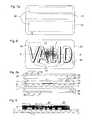
- the data carrier 27 in FIG. 8has a structured surface 11. These surface structures are out of the plane of the surface 11 raised and / or recessed in the surface 11 partial surfaces 33 of the Surface 11 composed and can be graphic motifs, pictures or Display texts in letters or braille; for example form the raised partial areas 33 in the drawing of FIG. 8 the word VALID.
- the protective layer 2( Figure 1) is transparent, the security element 3, the Indicia 10 (FIG. 1) in the text fields 29, 30, the photograph 26 (FIG. 7) etc. still visible on the information page 8 of the substrate 1.
- the figureshows a cross section along the line A / A 'through the data carrier 27 8a.
- the layer composite 7is produced in an injection mold 34, 35 which comprises an upper part 34 and a base part 35.
- upper part 34 and base part 35moved apart and the layer composite 7 between the Parts 34, 35 arranged the injection mold.
- That on the information page 8 arranged security element 3is completely in the protective layer 2 embedded and is covered by it.
- the protective layer 2protects the Information carriers 3, 10 ( Figure 1), 14 ( Figure 4), 26 ( Figure 6) on the Information page 8 and extends over the entire substrate 1.
- Die Partial areas 33project only about 0.1 mm above the plane of the surface 11, are still clearly visible and palpable. The one because of the molding The cross-sectional shape of the partial surfaces 33 resulting from the injection mold does not offer any Point of attack for mechanical destruction.
- the rational production of the layer composite 7takes place by injection molding Protective layer 2.
- the substrate 1with that on the information page 8 arranged information carrier 3, 10 (Figure 1), 14 ( Figure 4), 26 ( Figure 6) inserted into the base part 35 of the injection mold, the rear side 9 (FIG. 1) in Contact with the bottom surface 36 of the base part 35 comes.
- the two parts 34, 35are joined together and the injection mold closed, so that a cavity with the Volume of the protective layer 2 arises.
- flowable plasticis pressed into the cavity by heating, whereby Vent channels 39 in the upper part 34 complete filling of the cavity enable.
- the structure of the surface 11 and the partial surfaces 33is through a corresponding design of the inner surface 36 of the upper part 34 predetermined.
- the substrate 1 when the plastic is injected from the Floor surface 36can lift, the substrate 1 z. B. by means of negative pressure the bottom surface 36 held. Serve in the bottom surface 36 recessed intake 38, in which by means of a vacuum pump Negative pressure is generated.
- the protective layer 2 produced in this wayis typically at least the same thickness as the substrate 1, but is preferred Protective layer 2 at most twice as thick as the substrate 1. The use a too thin substrate 1 carries the risk that the substrate 1 when Injection molding folds, melts or later becomes like a laminating film pulls off.
- the injected plastic of the protective layer 2combines intimately with the Substrate 1 and the security element 3 and cools because of Heat capacity of the substrate 1 decreases so quickly that the substrate 1 and the information carriers (especially the security element 3) are not to be damaged.
- EP-401'466 A1describes the effects excessive heat supply to the security element 3.
- the information carrier 3, 10, 14, 26are heat-resistant connected to the material of the substrate 1, so that the information carrier 3, 10, 14, 26 when generating the Protective layer 2 or the intermediate layer 17 (FIG. 4) not from the substrate 1 solve and their predetermined arrangement is preserved. Any, after Form remaining remnants of a sprue 40 on the edge of the card eliminated by trimming the card shape.
- the protective layer 2 (or 2 ' and 17) and the substrate 1are sufficiently flexible to meet the requirements Flexibility of the data card is sufficient.
- polyesterssuch as Polyethylene terephthalate (PETP, Mylar®), polybutilenterephthalate (PBT), Polycarbonate (PC, Macrolon®) etc.
- polyolefinse.g. polyethylene (PE), polypropylene (PP), etc., or polymethyl methacrylate (PMMA) Copolymer, e.g. Acrylonitrile-butadiene-styrene copolymers (ABS), or Polyvinyl chloride (PVC), polyamide (PA) etc.
- PETPis already at sprayable at a temperature of 70-140 ° C, is characterized by a large Abrasion resistance and is gastight and dimensionally stable.
- These plasticsare also available as films for substrate 1. If the substrate 1 and the Protective layer 2 are made of suitable plastic materials, is the Connection between the substrate 1 and the protective layer 2 no longer separate and form a single card body. Optimal conditions are at given a layer composite 7, that for the substrate 1 and the protective layer 2 has the same plastics.
- Preferred materialsare ABS, PETP, PC, PMMA etc., which are both crystal clear and in transparent or opaque quality colored are available.
- the plasticscontain Another advantage is fluorescent dyes.
- the opaque qualitiesare more suitable for the substrate 1.
- the use of transparent qualities for the substrate 1enables the To consider security element 3 through the back 9 ( Figure 1).
- the Indicia 10, 14 on the information page and the information on the back 9represent inconspicuous patterns that only become clear when looking through letters, Put together numerals, graphic patterns, emblems and the like.
- Security elements 3also a machine readable by means of radiation Information, e.g. a general or an individual approval number that is represented by a combination of the diffraction elements 5 (FIG. 5), so is the protective layer 2 at least for the radiation for reading to be transparent.
- the machine-readable informationcan alone or together with visually visible patterns in the security element 3 be included.
- FIG. 9shows an embodiment of the layer composite 7 (FIG. 8a) with a generated according to the teaching of EP-741'370 A1 mentioned at the outset Security element 3 ( Figure 8a).
- the security element 3consists of small ones Laminate pieces 41, which are in the form of dots, rectangles, linear Area pieces with a very small width, typically smaller than 0.5 mm, etc., in a predetermined pattern as circular rings, guilloche, graphic Representations, lettering, etc. on the information page 8 are arranged.
- the laminate pieces 41together form the security element 3.
- In Cross section of the layer composite 7 shown in FIG. 9are from Security element 3 only the cuts through those glued to the substrate 1 Laminate pieces 41 visible.
- the protective layer 2has flat structures 42 molded into the surface 11 z.
- data carriers 27Figure 8 raised characters 43 of Braille provided to Obtainable disc 27 also for the visually impaired.
- the extension of the protective layer 2is, for example, in another Execution limited to part of the information page 8 of the substrate 1.
- the substrate 1 and the protective layer 2are particularly intimate because of the Connection at the common interface is inseparable connected.
Landscapes
- Engineering & Computer Science (AREA)
- General Physics & Mathematics (AREA)
- Theoretical Computer Science (AREA)
- Physics & Mathematics (AREA)
- Computer Hardware Design (AREA)
- Microelectronics & Electronic Packaging (AREA)
- Credit Cards Or The Like (AREA)
- Injection Moulding Of Plastics Or The Like (AREA)
- Structures Or Materials For Encapsulating Or Coating Semiconductor Devices Or Solid State Devices (AREA)
- Magnetic Record Carriers (AREA)
- Medicines That Contain Protein Lipid Enzymes And Other Medicines (AREA)
- Pharmaceuticals Containing Other Organic And Inorganic Compounds (AREA)
- Surgical Instruments (AREA)
- Superconductors And Manufacturing Methods Therefor (AREA)
- Optical Communication System (AREA)
Abstract
Description
Translated fromGermanDie Erfindung bezieht sich auf einen Datenträger nach dem Oberbegriff desAnspruchs 1 und ein Verfahren zur Herstellung eines solchen Datenträgersnach dem Oberbegriff des Anspruchs 14.The invention relates to a data carrier according to the preamble of
Solche Datenträger dienen als Identitätskarte (Personalausweis, Checkkarte,Abonnement für Transportunternehmen usw.), als elektronisches Zahlmittel(smart card), als Berechtigungsausweis für eine Zutrittskontrolle usw. undweisen als Echtheitsmerkmal wenigstens ein Sicherheitsmerkmal mitbeugungsoptisch wirksamen Strukturen auf.Such data carriers serve as an identity card (identity card, check card,Subscription for transport companies, etc.) as an electronic means of payment(smart card), as a credential for access control etc. andhave at least one security feature as authenticity featurestructures effective in diffraction.
Ein Datenträger ist aus der CH-PS 672'285 bekannt, der einen in Spritzgusserzeugten, massiven, aber flexiblen Körper aus Kunststoff mit einerAusnehmung zur Aufnahme von integrierten Schaltungen aufweist.A data carrier is known from CH-PS 672'285, the one in injection moldingproduced, massive but flexible plastic body with aHas recess for receiving integrated circuits.
Aus der WO 96/34730 ist ein Verfahren zum Herstellen von ein- oder beidseitigmit einem bedruckten Etikett versehene Kunststoffkarten bekannt, bei demzunächst die bedruckten, mit magnetischen Aufzeichnungsstreifen oderSicherheitsmerkmale mit beugungsoptisch wirksamen Strukturen versehenenEtiketten erzeugt werden. Die Rückseite der Etiketten bzw. zwischen denRückseiten zweier Etiketten wird in einer Spritzgussform Kunststoffmaterialangespritzt, um die von ISO vorgeschriebene Dicke der Ausweiskarten zu erhalten. Ausdrücklich werden hier auf die in der WO 96/34730 enthaltenentechnischen Details zum Bedrucken von Kunststoffkarten und denUeberlegungen zur Spritzgusstechnik verwiesen. Zum Schutz der auf demEtikett angebrachten Indicia gegen mechanische Einwirkungen wird eintransparenter Schutzlack aufgetragen.WO 96/34730 describes a method for producing on one or both sidesknown with a printed label plastic cards in whichfirst the printed, with magnetic recording strips orSecurity features with structures that are effective in diffraction opticsLabels are generated. The back of the labels or between theThe back of two labels is made of plastic material in an injection moldmolded to the thickness of the ID card specified by ISOreceive. We expressly refer to those contained in WO 96/34730technical details for printing on plastic cards and theConsiderations regarding injection molding technology. To protect the on theIndicia against mechanical impact will be attachedtransparent protective varnish applied.
Die EP-914'921 A1 beschreibt ein Verfahren und eine Vorrichtung zumSpritzgiessen von Codekarten. Die Codekarte besteht aus zwei gespritzten,flächigen Kunststoffschalen, die zur Codekarte zusammengefügt, einenHohlraum einschliessen, der Raum für eine Spule und andere Gegenstände,wie z.B. Kunststoff- oder Metallteile, Magnete, Hologramme, Photographien,usw., bietet.EP-914'921 A1 describes a method and an apparatus forInjection molding of code cards. The code card consists of two injection moldedflat plastic shells, which are put together to form a code card, oneInclude cavity, the space for a coil and other objects,such as. Plastic or metal parts, magnets, holograms, photographs,etc., offers.
Die EP-709'805 A2 lehrt Hologramme, Magnetstreifen und elektronischeModule in die Hauptflächen einer Datenkarte einzubetten, wobei elektronischeModule für einen berührungslosen Datenaustausch auch im Innern der Karteangeordnet sein können. Es wird kein Spritzgussverfahren angewendet,sondern ein Granulat verschiedenster Körnung zusammen mit demeingebetteten elektronischen Modul bei erhöhter Temperatur verpresst.EP-709'805 A2 teaches holograms, magnetic strips and electronic onesEmbed modules in the main areas of a data card, being electronicModules for contactless data exchange even inside the cardcan be arranged. No injection molding process is usedbut a granulate of various grain sizes together with theembedded electronic module pressed at elevated temperature.
In Laminate aus Kunststoff eingebettete Muster aus Beugungsstrukturen dienenals fälschungssichere Merkmale zur Beglaubigung der Echtheit wertvollerGegenstände. Besonders die visuell wahrnehmbaren Muster, Schriften usw.aus Beugungsstrukturen, die beim Drehen um eine der Achsen des Laminatsnacheinander sichtbar werden und einen sequentiellen Ablauf von Bildernerzeugen, sind z.B. aus den Patentschriften CH-PS 659'433, EP-330'738 A1,EP-375'833 A1, EP-537'439 A1 bekannt, während der Schichtaufbau derLaminate in der CH-PS 680'170, der EP-401'466 A1 usw. beschrieben ist.Serve patterns of diffraction structures embedded in plastic laminatesmore valuable as counterfeit-proof features to authenticate authenticityItems. Especially the visually perceptible patterns, fonts, etc.from diffraction structures that when rotating around one of the axes of the laminatebecome visible one after the other and a sequential sequence of imagesare e.g. from the patents CH-PS 659'433, EP-330'738 A1,EP-375'833 A1, EP-537'439 A1 known, during the layer structure of theLaminates in CH-PS 680'170, EP-401'466 A1, etc. is described.
Die CH-PS 678'835 zeigt einen Ausweis mit einer gegen ein Austauschengesicherten Photographie. Eine Marke aus dem Laminat mit dem Muster auseingebetteten Beugungsstrukturen überdeckt einen Teil der auf den Ausweisgeklebten Photographie des Inhabers und einen angrenzenden Teil desAusweises. Die Photographie steht wesentlich über der Oberfläche desDokuments vor, so dass die Marke im Bereich der von ihr abgedecktenBerandung der Photographie gerade dort besonders anfällig auf mechanischeBeschädigungen ist, wo eine unbefugtes Austauschen der Photographieüberprüft werden muss. Ein Abdecken des Ausweises mit einer Laminierfolieverzögert lediglich ein Auftreten von Beschädigungen.CH-PS 678'835 shows an ID card with one for an exchangesecured photograph. A stamp made from the laminate with the patternembedded diffraction structures covered part of the ID cardglued photograph of the holder and an adjacent part of theID. The photograph is significantly above the surface of theDocument so that the mark is in the area covered by itThe edges of photography are particularly vulnerable to mechanical onesDamage is where an unauthorized replacement of the photographneeds to be checked. Covering the ID with a laminating filmonly delays the occurrence of damage.
Nach der EP-741'370 A1 (= US 5 882 463) ist das ausunzusammenhängenden, kleinen Flächenteilen auf einem Datenträgerzusammengesetzte Sicherheitsmerkmal zum Schutz gegen ein Abstossen derFlächenteile ganz oder teilweise mit einem kratzfesten, bedruckbaren undvorteilhaft mit UV Strahlung zu härtenden Lack überzogen.According to EP-741'370 A1 (= US 5 882 463) this is overincoherent, small areas on a data carrierCompound security feature to protect against repelling theAll or part of the surface parts with a scratch-resistant, printable andadvantageously coated with UV radiation varnish.
Ein Nachteil der bekannten Ausweiskarten mit einem Sicherheitsmerkmal,insbesondere der "smart cards", der Identitätskarten usw., ist deren Anfälligkeitauf mechanische Beschädigungen, die in der langen Gebrauchsdauerauftreten. Die Ausweiskarten werden täglich mechanisch belastet, sei es imPortemonnaie oder sei es beim Einführen durch enge, metallischeBlendenöffnungen von Lesegeräten aller Art. Dies stellt an die Scheuerfestigkeitder Kartenoberfläche grosse Anforderungen, speziell wenn im Bereich desSicherheitsmerkmals und anderer Indicia die Ausweiskarten verdickt und daherdie Oberfläche nicht eben ist.A disadvantage of the known ID cards with a security feature,especially the "smart cards", the identity cards etc., is their vulnerabilityon mechanical damage that occurs in the long service lifeoccur. The ID cards are mechanically loaded daily, be it in theWallet or when inserting through tight, metallicApertures of readers of all kinds. This puts on the abrasion resistancethe map surface has great requirements, especially if in the area ofSecurity feature and other Indicia the ID cards thickened and thereforethe surface is not flat.
Die Aufgabe der Erfindung ist eine spannungsfreie, kostengünstigeAusweiskarte mit einer grossen Scheuerfestigkeit des Sicherheitsmerkmals zu schaffen und ein kostengünstiges Herstellverfahren für eine solcheAusweiskarte mit diesen Eigenschaften anzugeben.The object of the invention is a stress-free, inexpensiveID card with a high abrasion resistance of the security featurecreate and an inexpensive manufacturing process for suchIdentity card with these characteristics.
Die Lösung der Aufgabe gelingt durch die in den Ansprüche 1 und 14angegebenen Merkmale. Vorteilhafte Ausgestaltungen der Erfindung ergebensich aus den abhängigen Ansprüchen.The problem is solved by the in
Ausführungsbeispiele der Erfindung werden anhand der Zeichnungen (mitAusnahme der Fig. 1) näher erläutert.Embodiments of the invention are based on the drawings (withException of Fig. 1) explained in more detail.
Es zeigen:
Figur 1- schematisch einen Datenträger mit einem Sicherheitselement imQuerschnitt,
Figur 2- einen Datenträger mit Indicia und einer Ausnehmung für ein IC-Modul,
Figur 3- eine Auskleidung zur Aufnahme des IC-Moduls,
- Figur 4
- der Datenträger mit sichtbaren Elementen in zwei Ebenen,
Figur 5- einen Datenträger mit einem kontaktlosen IC-Modul,
Figur 6- einen Datenträger mit einem gesicherten Bild,
Figur 7- die Vorderseite eines Datenträgers,
- Figur 7a
- die Rückseite eines Datenträgers,
Figur 8- die Vorderseite eines Datenträgers mit einer lokal begrenztenSchutzschicht,
- Figur 8a
- einen Datenträger im Querschnitt mit einer Spritzform und
Figur 9- eine Schutzschicht mit Oberflächenstruktur.
- Figure 1
- schematically a data carrier with a security element in cross section,
- Figure 2
- a data carrier with indicia and a recess for an IC module,
- Figure 3
- a lining for holding the IC module,
- Figure 4
- the data carrier with visible elements in two levels,
- Figure 5
- a data carrier with a contactless IC module,
- Figure 6
- a disk with a saved image,
- Figure 7
- the front of a disk,
- Figure 7a
- the back of a disk,
- Figure 8
- the front of a data carrier with a locally limited protective layer,
- Figure 8a
- a disk in cross section with an injection mold and
- Figure 9
- a protective layer with a surface structure.
In der Figur 1 bedeutet 1 ein Substrat, 2 eine Schutzschicht, 3 einSicherheitselement mit einer Deckschicht 4 über einem Beugungselement 5einschliessenden Laminat 6. Die mit den Bezugszahlen 1 bis 6 bezeichnetenTeile bilden zusammen einen, in dieser Darstellung im Querschnitt gezeigtenSchichtverbund 7 für Datenträger. Dieser Schichtverbund 7 weist eine Dickevon weniger als 0,1 mm bis etwa 2 mm auf, wobei für einen typischen flächigenDatenträger gemäss ISO Norm 7816-1 die Abmessungen mit 85,4 mm x 54 mmbei einer Dicke von 0,76 mm festgelegt sind. Allerdings werden oft auch andereDicken im Bereich 0,6 mm bis 1,0 mm bevorzugt.In FIG. 1, 1 means a substrate, 2 a protective layer, 3 aSecurity element with a cover layer 4 over a
Das Substrat 1 ist ein flächiger Gegenstand aus Metall, Papier usw. oder einemKunststoff. Für Wertkarten hoher Qualität werden Folien aus Kunststoff miteiner Dicke von 0,1 mm bis zu 1.0 mm verarbeitet. In einem Beispiel ist dasSubstrat 1 aus einer bandförmigen Folie aus Kunststoff ausgestanzt. Die derSchutzschicht 2 zugewandte Seite des Substrats 1 ist die Informationsseite 8,die andere Seite des Substrats 1 ist die Rückseite 9. Das Substrat 1 weistwenigstens auf der Informationsseite 8 Indicia 10 auf, die drucktechnischerzeugt sind und/oder auch ein aufgeklebtes Bild, z.B. des Ausweisinhabers,umfassen können.The
Das Sicherheitselement 3 besteht aus einem Laminat 6 aus wenigstens zweiLackschichten. Zwischen zwei dieser Schichten sind die Beugungselemente 5eingebettet. Die Beugungselemente 5 können Hologramme sein oder bildenaus Teilflächen mit abgeformten, mikroskopisch feinen Reliefstrukturenzusammengesetzte Muster, Schriften oder Bildsequenzen, die in den eingangsgenannten Dokumenten beschrieben sind. Beim Kippen oder Drehen desSicherheitselements 3 sieht der Betrachter eine Veränderung der Muster, derSchriften oder einen Ablauf von Bildern einer Sequenz. DieSicherheitselemente 3 umfassen neben gewöhnlichen Hologrammen die eingangs erwähnten Sicherheitsmerkmale, die in den dort erwähnten Schriftenbeschrieben sind. Das Sicherheitselement 3 kann auf der Betrachtungsseiteeine bis zu 100 µm dicke, zähe transparente Deckschicht 4 aufweisen, die dasLaminat 6 vor mechanischem Abrieb schützt.The
Auf der von der Deckschicht 4 bzw. Betrachtungsseite abgewandten Fläche istdas Laminat 6 zum Kleben ausgerüstet, um das Sicherheitselement 3 auf derInformationsseite 8 mit dem Substrat 1 zu verbinden. An der mit einemmikroskopisch feinen Relief der Beugungselementen 5 strukturiertenGrenzfläche zwischen den beiden Lackschichten muss der Brechungsindexeinen Sprung aufweisen, damit das aus dem Halbraum der Betrachtungsseiteeinfallende und an den Beugungselementen 5 gebeugte Licht wieder in denHalbraum zurückgeworfen wird. Sind die beiden Lackschichten transparent undweisen sie eine Differenz im Brechungsindex auf, sind auch die unter demSicherheitselement 3 angeordneten Indicia 10 sichtbar. Ein transparentesDielektrikum mit hohem Brechungsindex, das als dünne Schicht auf derstrukturierten Grenzfläche aufgetragen ist, vergrössert den Reflexionsgradderart, dass die Indicia 10 nur unter den Raumwinkeln gut sichtbar sind, indenen kein gebeugtes Licht reflektiert wird. Anderseits reflektiert einmetallischer Ueberzug (Al, Au, Cu usw.) von mehr als 10 nm Dicke auf derstrukturierten Grenzfläche das gebeugte Licht fast vollständig, so dass die unterdem Sicherheitselement 3 angeordneten Indicia 10 nicht sichtbar sind, es seidenn, das Motiv des Sicherheitselement 3 besteht aus einem filigranen feinenLinienmuster, bei dem der metallische Ueberzug so im Bereich der Linienaufgebracht ist, dass die beugenden und reflektierenden Linien von neutralenvollständig transparenten Gebieten getrennt sind, eine Ausführung, die in dereingangs erwähnten EP-537'439 A1 beschrieben ist.On the surface facing away from the cover layer 4 or viewing sidethe
Die Ausführung des Schichtverbunds 7 in der Figur 2 weist in der Schutzschicht2 eine Vertiefung 13 für die Aufnahme eines Moduls mit einer integriertenSchaltung auf, die für elektronische vorbezahlte Wertkarten, Ausweiskarten,"smart cards", elektronische Geldbörsen usw. eingesetzt wird. Das Substrat 1weist auf der Informationsseite 8 wenigstens das Sicherheitselement 3 auf.Einige der Indicia 10 können durch das Sicherheitselement 3 hindurch sichtbarsein oder sind als Druckbild 14 über dem Sicherheitselement 3 angeordnet.Danach wird die Schutzschicht 2 aus transparentem Kunststoff aufgespritzt undgleichzeitig die Vertiefung 13 in die Schutzschicht 2 eingeformt. DasSicherheitselement 3 ist zwischen dem Substrat 1 und der Schutzschicht 2völlig fugenlos eingeschlossen.The embodiment of the
Bei der Ausführung nach der Figur 3 ist die Vertiefung 13 (Figur 2) mit einereinem Fingerhut ähnlichen Auskleidung 15 aus dünnem Metallblech oderKunststoff ausgefüttert, wobei das Metall als Schirm gegen elektrischeStörungen wirkt. Vor dem Spritzgiessen der Schutzschicht 2 ist die Auskleidung15 am Ort der Vertiefung 13 in der Spritzform so angeordnet, dass beimAufbringen der Schutzschicht 2 auf das mit dem Sicherheitselement 3 (Figur 2)bestückte Substrat 1 die Auskleidung 15 mit dem Kunststoff der Schutzschicht 2umspritzt wird und in der Schutzschicht 2 die ausgekleidete Vertiefung 13entsteht. Die Auskleidung 15 ist bündig mit der Oberfläche 11 (Figur 1) underweitert sich gegen die Oberfläche 11, um das Kontaktfeld des Moduls mit derintegrierten Schaltung aufzunehmen. Die Auskleidung 15 weist mit Vorteilwenigstens eine aussen auf ihrer Aussenseite umlaufende Rippe 16 und eineauf der Innenseite umlaufende Nut auf, damit sowohl die Auskleidung 15 in derSchutzschicht 2 als auch das zu einem späteren Zeitpunkt mit einerVerfüllmasse, z.B. mit dem unter der Marke Araldit® bekanntenZweikomponentenkleber, eingeklebte Modul mit der integrierten Schaltung inder ausgekleideten Vertiefung 13 durch die von der Rippe 16 und der Nut erzeugten Verzahnung sicher verankert ist. Bei einem dicken Substrat 1 kanndie aufgespritzte Schutzschicht für die Aufnahme der Auskleidung 15 zu dünnsein. Mit Vorteil wird am Ort der Vertiefung 13 in das Substrat 1 ein Lochgestanzt, das den unteren Teil der Auskleidung 15 aufnimmt, wobei beimErzeugen der Schutzschicht 2 der Kunststoff allfällige Freiräume in diesemLoch verfüllt.In the embodiment according to FIG. 3, the depression 13 (FIG. 2) has aa thimble-
Bei der Ausführung des Schichtverbunds 7 in der Figur 4 ist die Schutzschicht 2aus zwei Kunststoffschichten aufgebaut, der äusseren Schutzschicht 2' undeiner zwischen der äusseren Schutzschicht 2' und dem Substrat 1eingeschlossenen Zwischenschicht 17. Die Zwischenschicht 17 und dieäussere Schutzschicht 2' sind im Spritzgussverfahren sukzessive nach derjeweiligen Bestückung der Informationsfläche 8 (Figur 1) bzw. der Oberseite 18der Zwischenschicht 17 mit Informationsmitteln, z.B. Sicherheitselement 3,indicia 10, 10', Druckbild 14, 14' usw., erzeugt.When the
Eine andere Ausführung weist anstelle des aufgeklebten Sicherheitselements 3ein direkt auf dem Substrat 1 erzeugtes Beugungsmuster auf. DieInformationsfläche 8 ist mit einer Prägeschicht 19 aus einem thermoplastischenLack beschichtet und ein Relief mit der Beugungsstruktur 5 in diePrägeschicht 19 abgeformt. Die Beugungsstruktur 5 kann auch mit einemSchutzlack 20 zum Schutz des Reliefs während des Spritzvorgangs abgedecktsein. Die Prägeschicht 19 und der Schutzlack 20 bzw. die Zwischenschicht 17entsprechen den Schichten des Laminats 6 (Figur 1). Um die geforderteoptische Wirkung zu erzeugen, ist die strukturierte Grenzfläche derPrägeschicht 19 wie beim Laminat 6 (Figur 1) ausgeführt. Die auf derPrägeschicht 19 angeordneten Indicia 10, 10' und die Beugungsstrukturen 5sind von der in einem ersten Spritzvorgang aufgebrachten Zwischenschicht 17aus transparentem Kunststoff eingeschlossen und überdeckt. Die gegen die äussere Schutzschicht 2' angrenzende Oberseite 18 der Zwischenschicht 17trägt das Druckbild 14, 14' und/oder wenigstens ein weiteresSicherheitselement 3.Another embodiment has instead of the glued-on security element 3a diffraction pattern generated directly on the
In einer speziellen Ausführung weist die Oberseite 18 zusätzlich oderalleinstehend die von einem Spritzwerkzeug abgeformten, optisch wirksamenReliefstrukturen 21 auf, die das einfallende Licht als Fresnellinse, als einMosaik aus Beugungsmustern oder als Hologramm modifizieren. Die äussereSchutzschicht 2' deckt das Druckbild 14 und/oder das Sicherheitselement 3und/oder die Reliefstrukturen 21 ab, wobei die strukturierte Grenzflächewenigstens im Bereich der Reliefstrukturen 21 wie beim Sicherheitselement 3so ausgeführt ist, dass ein Sprung im Brechungsindex entsteht, damit diegeforderte optische Wirkung erzeugt wird. Die Herstellung durch Spritzgussweist als Vorteil eine grosse Genauigkeit in der Dicke der Zwischenschicht 17auf. Insbesondere ist das optische Zusammenwirken der Informationsmittel aufder Oberseite 18 mit den Informationsmitteln auf der Informationsseite 8 durchdie Dicke der Zwischenschicht 17 mitbestimmt. Die Anordnung derInformationsmittel (Sicherheitselemente 3, Beugungsstrukturen 5, Indicia 10,10', Druckbilds 14, 14', Reliefstrukturen 21 usw.) kann im Register ausgeführtsein, wobei die damit erzielbaren optischen Wirkungen in der WO 97/19820beschrieben sind.In a special embodiment, the top 18 additionally has orstand alone the optically effective molded from an injection
Die Figur 5 zeigt eine Ausführung des Schichtverbunds 7 mit einer gemäss dereingangs erwähnten EP-709'805 A2 über Antennen 22 mit der Aussenwelt inVerbindung bringbaren integrierten Schaltung 23, die zusammen mit demSicherheitselement 3 im Schichtverbund 7 enthalten sind.FIG. 5 shows an embodiment of the
Eine andere Ausführung des Schichtverbunds 7 weist eine aus wenigstens zweiPortionen 24, 25 aus sich unterscheidenden Kunststoffmaterialien aufgebaute Schutzschicht 2 (Figur 2) auf. Im gezeichneten Beispiel sind beim Spritzen dieflüssigen Kunststoffe von der linken und von der rechten Seite desSchichtverbunds 7 zugeführt worden. Entsprechend den beim Spritzenverwendeten Drücken fliessen die Kunststoffe verschieden schnell über dieInformationsseite 8 (Figur 1) und treffen an einer vorbestimmten Stelleaufeinander. Mit Vorteil erfolgt das Spritzen der Schutzschicht 2 in zweiSchritten, wobei zuerst die erste Portion 24 mit dem einen Kunststoff auf dasSubstrat 1, z.B. im Bereich des Sicherheitselements 3, aufgetragen wird undanschliessend der andere Kunststoff für die zweite Portion 25 gespritzt wird. Beieiner Kombination dieser Ausführung mit der Ausführungsvariante gemäss derFigur 4 weist die erste Portion 24 nur die Dicke der Zwischenschicht 17(Figur 4) auf und bedeckt das Substrat 1, z.B. im Bereich desSicherheitselements 3. Die zweite Portion 25 wird in der Dicke derSchutzschicht 2 aufgebracht, wobei die zweite Portion 25 im Bereich der erstenPortion 24 nur die Dicke der äusseren Schutzschicht 2' (Figur 4) erhält. Für dasSpritzen der Kunststoffe in mehreren Schritten werden für jeden Schritt dieentsprechenden Spritzformen benötigt.Another embodiment of the
Die Kunststoffe sind so gewählt, dass sie eine innige Verbindung nicht nur zumSubstrat 1 bzw. zum Laminat 6 (Figur 1) des Sicherheitselementes 3 eingehensondern auch zwischen den Portionen 24, 25. Beispielsweise unterscheidensich die Kunststoffe der beiden Portionen 24, 25 lediglich durch ihreTransparenz oder Einfärbung. Die Schutzschicht 2 gewährleistet im Bereich desSicherheitselementes 3 die visuelle und/oder die maschinelle Erkennbarkeit desSicherheitselementes 3 im vorbestimmten Bereich der Wellenlänge derelektromagnetischen Strahlung.The plastics are chosen in such a way that they not only create an intimate connection to the
In der Figur 6 enthält der Schichtverbund 7 eine auf der Informationsseite 8 aufdem Substrat 1 aufgeklebte Photographie 26 mit einem als Beglaubigungsmarke über einem Teil der Photographie 26 angeordnetenSicherheitsmerkmal 3. Gegenüber dem Gegenstand in der als Stand derTechnik eingangs erwähnten CH-PS 678'835 ist der Vorteil desSchichtverbunds 7 offensichtlich, dass der Schutz der beglaubigtenPhotographie 26 mittels der Schutzschicht 2 gegen mechanische Einflüsseverbessert ist. Die völlig glatte, zur Rückseite 9 planparallele Oberfläche 11weist keinerlei Angriffspunkte für mechanische Einflüsse auf. DerSchichtverbund 7 weist keine Beschichtung mit dünnen Kunststoffolien an derOberfläche 11 oder an der Rückseite 9 (Figur 1) auf, die sich im Laufe desGebrauchs ablösen können.In FIG. 6, the
In der Figur 7 ist der Schichtverbund 7 (Figur 6) als flächiger Datenträger 27geformt. Der Datenträger 27 weist auf der Informationsseite 8 (Figur 6) inbeispielhafter Weise angeordnete, durch die Schutzschicht 2 (Figur 6) hindurchsichtbare Informationsträger auf, z.B. die Photographie 26 und das diePhotographie 26 teilweise überlappende Sicherheitselement 3, Textfelder 29,30 usw. In den Textfeldern 29, 30 sind die Indicia 10 (Figur 1) bzw. dieDruckbilder 14 (Figur 4) in wenigstens einer Ebene untergebracht. DasSicherheitselement 3 und die dicke Schutzschicht 2 verhindern wirksam einenAustausch der Photographie 26. Die Ausrüstung des Datenträgers 27 wirdgegebenenfalls durch das Modul mit der integrierten Schaltung für elektronischveränderbare Daten vervollständigt, wobei in der Ansicht der Figur 7 nur einKontaktfeld 28 für den Datenaustausch mit der integrierten Schaltung sichtbarist.In FIG. 7, the layer composite 7 (FIG. 6) is a
Der Datenträger 27 ist in der Figur 7a von der Rückseite 9 dargestellt. DieRückseite 9 kann mit einem Informationsstreifen 31 parallel zurLängsausdehnung des Datenträgers 27 beklebt werden, beispielsweise einemStreifen mit einer magnetisierbaren Schicht oder einen aus der EP-718'795 A1 bekannten Streifen mit optischen Markierungen. Beidseits desInformationsstreifens 31 ist in Teilbereichen 32 der Rückseite 9 die mitultravioletter Strahlung gehärtete Lackschicht 12 (Figur 1) aufgetragen. DieserAuftrag schützt einerseits den Informationsstreifen 31, da er gegenüber derLackoberfläche vertieft ist, andererseits durch Überdecken eine in denTeilbereichen 32 visuell erkennbare Information. Die Lackschicht 12 kann eineinfaches Punktmuster bilden oder ist vollflächig aufgetragen.The
Der Datenträger 27 in der Figur 8 weist eine strukturierte Oberfläche 11 auf.Diese Oberflächenstrukturen sind aus über die Ebene der Oberfläche 11erhabenen und/oder in die Oberfläche 11 eingetieften Teilflächen 33 derOberfläche 11 zusammengesetzt und können graphische Motive, Bilder oderTexte in Buchstaben oder auch Blindenschrift darstellen; beispielsweise bildendie erhabenen Teilflächen 33 in der Zeichnung der Figur 8 das Word VALID. Dadie Schutzschicht 2 (Figur 1) transparent ist, sind das Sicherheitselement 3, dieIndicia 10 (Figur 1) in den Textfeldern 29, 30, die Photographie 26 (Figur 7)usw. auf der Informationsseite 8 des Substrats 1 trotzdem sichtbar.The
Einen Querschnitt längs der Linie A/A' durch den Datenträger 27 zeigt die Figur8a. Die Herstellung des Schichtverbunds 7 erfolgt in einer Spritzform 34, 35, dieein Oberteil 34 und ein Basisteil 35 umfasst. In der Zeichnung sind Oberteil 34und Basisteil 35 auseinander gefahren und der Schichtverbund 7 zwischen denTeilen 34, 35 der Spritzform angeordnet. Das auf der Informationsseite 8angeordnete Sicherheitselement 3 ist vollständig in der Schutzschicht 2eingebettet und wird von ihr überdeckt. Die Schutzschicht 2 schützt dieInformationsträger 3, 10 (Figur 1), 14 (Figur 4), 26 (Figur 6) auf derInformationsseite 8 und erstreckt sich über das ganze Substrat 1. DieTeilflächen 33 stehen nur etwa 0,1 mm über die Ebene der Oberfläche 11 vor,sind aber dennoch gut sichtbar und auch ertastbar. Die wegen des Ausformens aus der Spritzform bedingte Querschnittsform der Teilflächen 33 bietet keinenAngriffspunkt für eine mechanische Zerstörung.The figure shows a cross section along the line A / A 'through the
Die rationelle Herstellung des Schichtverbunds 7 erfolgt durch Spritzgiessen derSchutzschicht 2. Das Substrat 1 mit dem auf der Informationsseite 8angeordneten Informationsträger 3, 10 (Figur 1), 14 (Figur 4), 26 (Figur 6) wirdin das Basisteil 35 der Spritzform eingelegt, wobei die Rückseite 9 (Figur 1) inKontakt mit der Bodenfläche 36 des Basisteils 35 kommt. Anschliessendwerden die beiden Teile 34, 35 zusammengefügt und die Spritzformgeschlossen, so dass über der Informationsseite 8 ein Hohlraum mit demVolumen der Schutzschicht 2 entsteht. Durch einen Einspritzkanal 37 wird derdurch Erwärmen fliessfähige Kunststoff in den Hohlraum eingepresst, wobeiEntlüftungskanäle 39 im Oberteil 34 ein vollständiges Füllen des Hohlraumsermöglichen. Die Struktur der Oberfläche 11 und der Teilflächen 33 ist durcheine entsprechende Ausbildung der Innenfläche 36 des Oberteils 34vorbestimmt.The rational production of the
Damit das Substrat 1 beim Einspritzen des Kunststoffs nicht von derBodenfläche 36 abheben kann, wird das Substrat 1 z. B. mittels Unterdruck aufder Bodenfläche 36 festgehalten. Dazu dienen in die Bodenfläche 36eingelassene Ansaugstutzen 38, in denen mittels einer VakuumpumpeUnterdruck erzeugt wird. Typischerweise ist die so hergestellte Schutzschicht 2wenigstens gleich dick wie das Substrat 1, bevorzugt jedoch ist dieSchutzschicht 2 höchstens doppelt so dick wie das Substrat 1. Die Verwendungeines zu dünnen Substrats 1 birgt die Gefahr, dass das Substrat 1 beimSpritzgiessen Falten wirft, aufschmilzt oder sich später wie eine Laminierfolieabziehen lässt.So that the
Der eingespritzte Kunststoff der Schutzschicht 2 verbindet sich innig mit demSubstrat 1 und dem Sicherheitselement 3 und kühlt sich dabei aber wegen derWärmekapazität des Substrats 1 doch so schnell ab, dass das Substrat 1 unddie Informationsträger (vor allem das Sicherheitselement 3) dennoch nichtbeschädigt werden. Die EP-401'466 A1 beschreibt die Auswirkungenexzessiver Wärmezufuhr auf das Sicherheitselement 3. Die Informationsträger3, 10, 14, 26 sind wärmefest mit dem Material des Substrats 1 verbunden,damit sich die Informationsträger 3, 10, 14, 26 beim Erzeugen derSchutzschicht 2 bzw. der Zwischenschicht 17 (Figur 4) nicht vom Substrat 1lösen und deren vorbestimmte Anordnung erhalten bleibt. Allfällige, nach demAusformen verbleibende Reste eines Angusses 40 am Kartenrand werdendurch ein Nachschneiden der Kartenform beseitigt. Die Schutzschicht 2 (bzw. 2'und 17) und das Substrat 1 sind genügend flexibel, um den Anforderungen anBiegsamkeit der Datenkarte zu genügen.The injected plastic of the
Für die Herstellung des Schichtverbunds 7 gemäss der Zeichnung der Figur 4sind zwei Spritzformen 34 (Figur 8a), 35 (Figur 8a) notwendig, eine erste, dieden Spritzguss für die Zwischenschicht 17 ermöglicht, und eine zweite für denSpritzguss der äusseren Schutzschicht 2'. Es ist ausreichend nur das Oberteil34 auszuwechseln, um den jeweils für den Spritzguss notwendigen Hohlraumsicherzustellen.For the production of the
Zurück zur Figur 8a. Als Kunststoffmaterialien zum Spritzen der Schutzschicht 2eignen sich unter anderen die Gruppe der Polyester, wie z.B.Polyaethylenterephtalat (PETP, Mylar®), Polybutilenterephtalat (PBT),Polycarbonat (PC, Macrolon®) usw., oder Polyolefine, wie z.B. Polyaethylen(PE), Polypropylen (PP) usw., oder Polymethylmethacrylat (PMMA), einCopolymer, wie z.B. Acrylnitril-Butadien-Styrol-Copolymere (ABS), oderPolyvinylchlorid (PVC), Polyamid (PA) usw. Insbesondere ist PETP schon bei einer Temperatur von 70-140°C spritzfähig, zeichnet sich durch eine grosseAbriebfestigkeit aus und ist gasdicht und dimensionsstabil. Diese Kunststoffesind auch als Folien für das Substrat 1 erhältlich. Wenn das Substrat 1 und dieSchutzschicht 2 aus geeigneten Kunststoffmaterialien hergestellt sind, ist dieVerbindung zwischen dem Substrat 1 und der Schutzschicht 2 nicht mehr zutrennen und bildet einen einzigen Kartenkörper. Optimale Verhältnisse sind beieinem Schichtverbund 7 gegeben, der für das Substrat 1 und die Schutzschicht2 gleiche Kunststoffe aufweist. Bevorzugte Materialien sind ABS, PETP, PC,PMMA usw., die sowohl glasklar als auch in transparenter oder opaker Qualitäteingefärbt lieferbar sind. Beispielsweise kann die Schutzschicht 2 für das visuellwahrnehmbare Licht und die angrenzenden Teile des Spektrums derelektromagnetischen Strahlung völlig transparent (= "glasklar") oder fürwenigstens einen Teil des sichtbaren Wellenlängenbereichs oder nur für dasvisuell nicht wahrnehmbare Licht transparent sein. Die Kunststoffe enthalten mitVorteil auch fluoreszierende Farbstoffe als Erkennungsmerkmal.Back to Figure 8a. As plastic materials for spraying the
Die opaken Qualitäten eignen sich eher für das Substrat 1. Die Verwendungvon transparenten Qualitäten für das Substrat 1 ermöglicht es, dasSicherheitselement 3 durch die Rückseite 9 (Figur 1) hindurch zu betrachten.Zudem können durch registerhaltiges Drucken der Indicia 10 (Figur 1), 14 (Figur2) auf der Informationsseite 8 (Figur 1) und der Informationen auf der Rückseite9 (Figur 1) sogenannte Durchsichtsregister geschaffen werden, wobei dieIndicia 10, 14 auf der Informationsseite und die Informationen auf der Rückseite9 unauffällige Muster darstellen, die sich erst in der Durchsicht zu Buchstaben,Ziffern, graphischen Mustern, Emblemen und dergleichen zusammensetzen.The opaque qualities are more suitable for the
Enthalten die in den beschriebenen Ausführungen verwendetenSicherheitselemente 3 auch eine mittels Strahlung maschinell auslesbare Information, z.B. eine allgemeine oder eine individuelle Zulassungsnummer, diedurch eine Kombination aus den Beugungselementen 5 (Figur 5) dargestellt ist,so ist die Schutzschicht 2 wenigstens für die Strahlung zum Auslesentransparent zu gestalten. Die maschinell auslesbare Information kann alleineoder zusammen mit visuell sichtbaren Mustern im Sicherheitselement 3enthalten sein. Weist das Sicherheitselement 3 nur mittels infraroter Strahlungmaschinell auszulesende Beugungselemente 5 auf, kann beispielsweise dieSchutzschicht 2 nur für infrarotes Licht transparent sein; für visuelles Lichthingegen ist die Schutzschicht 2 undurchsichtig und beispielsweise schwarzeingefärbt. Besteht das Substrat 1 aus einem Kunststoff mit dieser Qualität,kann auch ein Auslesen der Information durch das Substrat 1 hindurch erfolgen.Contain the used in the described
Die Figur 9 zeigt eine Ausführung des Schichtverbunds 7 (Figur 8a) mit einemgemäss der Lehre der eingangs erwähnten EP-741'370 A1 erzeugtenSicherheitselement 3 (Figur 8a). Das Sicherheitselement 3 besteht aus kleinenLaminatstücken 41, die in Form von Punkten, Rechtecken, linienförmigenFlächenstücken mit sehr kleiner Breite, typisch kleiner als 0.5 mm, usw., ineinem vorbestimmten Muster als Kreisringe, Guillochen, graphischeDarstellungen, Schriftzüge usw. auf der Informatiönsseite 8 angeordnet sind.Die Laminatstücke 41 bilden zusammen das Sicherheitselement 3. Imdargestellten Querschnitt des Schichtverbunds 7 der Figur 9 sind vomSicherheitselement 3 nur die Schnitte durch die auf das Substrat 1 aufgeklebtenLaminatstücke 41 sichtbar.FIG. 9 shows an embodiment of the layer composite 7 (FIG. 8a) with agenerated according to the teaching of EP-741'370 A1 mentioned at the outsetSecurity element 3 (Figure 8a). The
Die Schutzschicht 2 weist in die Oberfläche 11 eingeformte flache Strukturen 42z. B. einer Fresnellinse auf. Als eine weitere Strukturierung sind für Datenträger27 (Figur 8) erhabene Zeichen 43 der Braille-Blindenschrift vorgesehen, umauch für Sehbehinderte unterscheidbare Datenträger 27 zu erhalten.The
Die Ausdehnung der Schutzschicht 2 ist beispielsweise in einer anderenAusführung auf einen Teil der Informationsseite 8 des Substrats 1 begrenzt.Das Substrat 1 und die Schutzschicht 2 sind wegen der besonders innigenVerbindung an der gemeinsamen Grenzfläche untrennbar miteinanderverbunden.The extension of the
Die verschiedenen Merkmale der hier aufgeführten Ausführungen sind beliebigkombinierbar. Insbesondere kann die freie Oberfläche 11, 11' auchherkömmlich bedruckt werden.The various features of the versions listed here are arbitrarycombined. In particular, the
Der Vorteil bei all diesen Ausführungen ist der bessere Schutz aller Indicia aufder Informationsseite 8 (Figur 6) bzw. auf der Oberseite 18 (Figur 4) undinsbesondere des Sicherheitselements 3 (Figur 2) gegen betrügerischeManipulationen oder Vandalismus, aber auch gegen Abrieb und Kratzer, die imtäglichen Gebrauch nicht zu vermeiden sind.The advantage of all these designs is the better protection of all indiciathe information page 8 (Figure 6) or on the top 18 (Figure 4) andin particular the security element 3 (FIG. 2) against fraudulent onesTampering or vandalism, but also against abrasion and scratches in thedaily use are unavoidable.
Claims (14)
Translated fromGermandadurch gekennzeichnet ,dass die Schutzschicht (2) aus einem spritzgussfähigen Kunststoffmaterialbesteht und das Sicherheitselement (3) und wenigstens teilweise dieInformationsseite (8) des Substrats (1) so bedeckt, dass dasSicherheitselement (3) zwischen dem Substrat (1) und der Schutzschicht (2)fugenlos eingeschlossen ist, und dass die Dicke der Schutzschicht (2)ausserhalb des Bereiches des Sicherheitselements (3) bzw. zusammen mitdem Sicherheitselement (3) wenigstens gleich der Dicke des Substrats (1)ist.Data carrier (27) made of a layered composite (7) with a substrate (1) formed by a flat object made of metal, paper or plastic, with a protective layer (2) connected to the substrate (1) and with at least one security element (3), which consists of a laminate (6) - with or without a cover layer (4) - with embedded diffraction elements (5) and is fixed on an information side (8) of the substrate (1) facing the protective layer (2)
characterized in that the protective layer (2) consists of an injection-moldable plastic material and covers the security element (3) and at least partially the information side (8) of the substrate (1) such that the security element (3) between the substrate (1) and the Protective layer (2) is seamlessly enclosed, and that the thickness of the protective layer (2) outside the area of the security element (3) or together with the security element (3) is at least equal to the thickness of the substrate (1).
dadurch gekennzeichnet ,dass die Schutzschicht (2) höchstens die doppelte Dicke des Substrats (1) aufweist.Data carrier according to claim 1,
characterized in that the protective layer (2) has at most twice the thickness of the substrate (1).
dadurch gekennzeichnet ,dass das Substrat (1) und/oder die Schutzschicht (2) transparent ist undwenigstens ein auf der Informationsseite (8) angeordnetesSicherheitselement (3) durch die transparente Schutzschicht (2) und/oderdurch das transparente Substrat (1) hindurch sichtbar ist.Data carrier according to claim 1 or 2,
characterized in that the substrate (1) and / or the protective layer (2) is transparent and at least one security element (3) arranged on the information side (8) through the transparent protective layer (2) and / or through the transparent substrate (1) is visible through it.
dadurch gekennzeichnet ,dass auf der Informationsseite (8) wenigstens ein weitererInformationsträger (10, 10'; 26) vorhanden ist, der zwischen dem Substrat(1) und der Schutzschicht (2) bzw. dem Sicherheitselement (3) angeordnetist.Data carrier according to one of claims 1 to 3,
characterized in that on the information side (8) there is at least one further information carrier (10, 10 '; 26) which is arranged between the substrate (1) and the protective layer (2) or the security element (3).
dadurch gekennzeichnet ,dass der Informationsträger eine sich teilweise mit dem Sicherheitselement(3) überlappende Photographie (26) ist.Data carrier according to claim 4,
characterized in that the information carrier is a photograph (26) partially overlapping with the security element (3).
dadurch gekennzeichnet ,dass auf der Informationsseite (8) ein Druckbild (14, 14') aufgebracht ist, daszwischen der Schutzschicht (2) und dem Sicherheitselement (3) bzw. demSubstrat (1) angeordnet ist.Data carrier according to claim 4 or 5,
characterized in that a printed image (14, 14 ') is applied to the information page (8) and is arranged between the protective layer (2) and the security element (3) or the substrate (1).
dadurch gekennzeichnet ,dass die Schutzschicht (2) und das Substrat (1) aus transparentemKunststoff bestehen, dass Indicia (10; 10'; 14; 14') auf der Informationsseite(8) des Substrats (1) im Register zu einer drucktechnisch aufgebrachtenInformation auf der Rückseite (9) des Substrats (1) angeordnet sind unddass wenigstens Teile der Indicia (10; 10'; 14; 14') und Teile derdrucktechnisch aufgebrachten Information auf der Rückseite (9)Durchsichtsregister bilden, die Buchstaben, Ziffern, graphische Muster,Embleme umfassen.Data carrier according to one of claims 1 to 6,
characterized in that the protective layer (2) and the substrate (1) consist of transparent plastic that Indicia (10; 10 ';14;14') on the information side (8) of the substrate (1) in the register to a printing technology applied Information is arranged on the back (9) of the substrate (1) and that at least parts of the indicia (10; 10 ';14;14') and parts of the information printed on the back (9) form transparent registers, the letters, numbers , graphic patterns, emblems include.
dadurch gekennzeichnet ,dass die Schutzschicht (2) aus einer äusseren Schutzschicht (2') und einerZwischenschicht (17) besteht, wobei die Zwischenschicht (17) zwischen deräusseren Schutzschicht (2') und dem Substrat (1) eingeschlossenen ist, unddass auf der an die äussere Schutzschicht (2') angrenzenden Oberseite (18)der Zwischenschicht (17) zusätzliche Informationsmittel angeordnet sind.Data carrier according to one of claims 1 to 7,
characterized in that the protective layer (2) consists of an outer protective layer (2 ') and an intermediate layer (17), the intermediate layer (17) being enclosed between the outer protective layer (2') and the substrate (1), and that Additional information means are arranged on the upper side (18) of the intermediate layer (17) adjoining the outer protective layer (2 ').
dadurch gekennzeichnet ,dass die Schutzschicht (2) aus PA, PC, PE, PETP, PMMA, PP, PVC oderABS besteht.Data carrier according to one of claims 1 to 8,
characterized in that the protective layer (2) consists of PA, PC, PE, PETP, PMMA, PP, PVC or ABS.
dadurch gekennzeichnet ,dass das Substrat (1) und die Schutzschicht (2) aus demselben Kunststoffbestehen.Data carrier according to claim 9,
characterized in that the substrate (1) and the protective layer (2) consist of the same plastic.
dadurch gekennzeichnet ,dass die Schutzschicht (2) in wenigstens zwei aneinandergrenzendePortionen (24; 25) eingeteilt ist, die sich wenigstens hinsichtlich derEinfärbung des Kunststoffmaterials unterscheiden.Data carrier according to one of claims 1 to 10,
characterized in that the protective layer (2) is divided into at least two adjoining portions (24; 25) which differ at least in terms of the coloration of the plastic material.
dadurch gekennzeichnet ,dass die Schutzschicht (2) und das Substrat (1) eine integrierteelektronische Schaltung (23) mit Antennen (22) einschliessen, wobei dieAntennen (22) zur Aufnahme von Verbindungen mit der Aussenwelt dienen.Data carrier according to one of claims 1 to 11,
characterized in that the protective layer (2) and the substrate (1) include an integrated electronic circuit (23) with antennas (22), the antennas (22) serving to establish connections with the outside world.
dadurch gekennzeichnet ,dass die Schutzschicht (2) eine Vertiefung (13) mit einer sich nach derOberseite (11) der Schutzschicht (2) öffnenden Auskleidung (15) zurAufnahme eines integrierten Moduls mit einer elektronischen Schaltung (23)aufweist, und dass die Auskleidung (15) auf ihrer Aussenseite mit Rippen(16) zur Verankerung in der Schutzschicht (2; 2', 17) und auf der Innenseitemit Nuten zur Verankerung des Moduls ausgestattet ist.Data carrier according to one of claims 1 to 12,
characterized in that the protective layer (2) has a recess (13) with a lining (15) opening towards the top (11) of the protective layer (2) for receiving an integrated module with an electronic circuit (23), and that Lining (15) on the outside with ribs (16) for anchoring in the protective layer (2; 2 ', 17) and on the inside with grooves for anchoring the module.
gekennzeichnet durch die Verfahrensschritte
characterized by the process steps
Priority Applications (3)
| Application Number | Priority Date | Filing Date | Title |
|---|---|---|---|
| ES03018198TES2320869T3 (en) | 1999-08-12 | 1999-08-12 | DATA SUPPORT. |
| DE59914972TDE59914972D1 (en) | 1999-08-12 | 1999-08-12 | disk |
| EP03018198AEP1388808B1 (en) | 1999-08-12 | 1999-08-12 | Data carrier |
Applications Claiming Priority (2)
| Application Number | Priority Date | Filing Date | Title |
|---|---|---|---|
| EP99115844AEP1076315B1 (en) | 1999-08-12 | 1999-08-12 | Data carrier |
| EP03018198AEP1388808B1 (en) | 1999-08-12 | 1999-08-12 | Data carrier |
Related Parent Applications (2)
| Application Number | Title | Priority Date | Filing Date |
|---|---|---|---|
| EP99115844.5Division | 1999-08-12 | ||
| EP99115844ADivisionEP1076315B1 (en) | 1999-08-12 | 1999-08-12 | Data carrier |
Publications (2)
| Publication Number | Publication Date |
|---|---|
| EP1388808A1true EP1388808A1 (en) | 2004-02-11 |
| EP1388808B1 EP1388808B1 (en) | 2009-03-04 |
Family
ID=8238764
Family Applications (2)
| Application Number | Title | Priority Date | Filing Date |
|---|---|---|---|
| EP99115844AExpired - LifetimeEP1076315B1 (en) | 1999-08-12 | 1999-08-12 | Data carrier |
| EP03018198AExpired - LifetimeEP1388808B1 (en) | 1999-08-12 | 1999-08-12 | Data carrier |
Family Applications Before (1)
| Application Number | Title | Priority Date | Filing Date |
|---|---|---|---|
| EP99115844AExpired - LifetimeEP1076315B1 (en) | 1999-08-12 | 1999-08-12 | Data carrier |
Country Status (6)
| Country | Link |
|---|---|
| EP (2) | EP1076315B1 (en) |
| AT (2) | ATE424589T1 (en) |
| DE (1) | DE59911557D1 (en) |
| DK (1) | DK1076315T3 (en) |
| ES (1) | ES2236997T3 (en) |
| PT (1) | PT1076315E (en) |
Cited By (2)
| Publication number | Priority date | Publication date | Assignee | Title |
|---|---|---|---|---|
| DE102006052651A1 (en)* | 2006-11-08 | 2008-05-15 | Giesecke & Devrient Gmbh | Portable data carrier |
| EP1580025B1 (en) | 2004-03-26 | 2015-10-14 | Hueck Folien Ges.m.b.H | Security element with features which can be recognised under a specific viewing angle |
Families Citing this family (6)
| Publication number | Priority date | Publication date | Assignee | Title |
|---|---|---|---|---|
| JP2755702B2 (en)* | 1989-07-27 | 1998-05-25 | 株式会社東芝 | Wear-resistant material |
| DE10254499B4 (en)* | 2002-11-22 | 2005-12-22 | Ovd Kinegram Ag | Layer arrangement with a lens-like effect generating diffractive optical effective structure |
| FR2849708B1 (en)* | 2003-01-03 | 2005-03-11 | Banque De France | WAVEGUIDE SECURITY DEVICE |
| DE10333704B4 (en) | 2003-07-23 | 2009-12-17 | Ovd Kinegram Ag | Security element for RF identification |
| DE10342276A1 (en)* | 2003-09-12 | 2005-04-07 | Bundesdruckerei Gmbh | Security document and method for producing a security document |
| GB0330008D0 (en)* | 2003-12-23 | 2004-01-28 | Security Printing And Systems | Anti-tamper documents |
Citations (7)
| Publication number | Priority date | Publication date | Assignee | Title |
|---|---|---|---|---|
| US4304809A (en)* | 1978-12-14 | 1981-12-08 | Hoechst Aktiengesellschaft | Identity card with grid images |
| US4463971A (en)* | 1981-04-14 | 1984-08-07 | Gao Gesellschaft Fur Automation Und Organisation Mbh | Identification card having an IC module |
| US5304513A (en)* | 1987-07-16 | 1994-04-19 | Gao Gesellschaft Fur Automation Und Organisation Mbh | Method for manufacturing an encapsulated semiconductor package using an adhesive barrier frame |
| EP0717389A1 (en)* | 1994-12-14 | 1996-06-19 | Plasto S.A. | Tamper-proof identification device |
| US5681356A (en)* | 1991-05-10 | 1997-10-28 | Gao Gesellschaft Fur Automation Und Organisation Mbh | Method and apparatus for producing a plastic molded chip card having reduced wall thickness |
| US5882463A (en)* | 1995-05-05 | 1999-03-16 | Landis & Gyr Technology Innovation Ag | Method of applying a security element to a substrate |
| EP0914921A1 (en)* | 1997-11-07 | 1999-05-12 | HERBST, Richard | Method and apparatus for injection moulding of coded cards |
- 1999
- 1999-08-12DKDK99115844Tpatent/DK1076315T3/enactive
- 1999-08-12ATAT03018198Tpatent/ATE424589T1/enactive
- 1999-08-12EPEP99115844Apatent/EP1076315B1/ennot_activeExpired - Lifetime
- 1999-08-12PTPT99115844Tpatent/PT1076315E/enunknown
- 1999-08-12ESES99115844Tpatent/ES2236997T3/ennot_activeExpired - Lifetime
- 1999-08-12EPEP03018198Apatent/EP1388808B1/ennot_activeExpired - Lifetime
- 1999-08-12DEDE59911557Tpatent/DE59911557D1/ennot_activeExpired - Lifetime
- 1999-08-12ATAT99115844Tpatent/ATE288600T1/enactive
Patent Citations (7)
| Publication number | Priority date | Publication date | Assignee | Title |
|---|---|---|---|---|
| US4304809A (en)* | 1978-12-14 | 1981-12-08 | Hoechst Aktiengesellschaft | Identity card with grid images |
| US4463971A (en)* | 1981-04-14 | 1984-08-07 | Gao Gesellschaft Fur Automation Und Organisation Mbh | Identification card having an IC module |
| US5304513A (en)* | 1987-07-16 | 1994-04-19 | Gao Gesellschaft Fur Automation Und Organisation Mbh | Method for manufacturing an encapsulated semiconductor package using an adhesive barrier frame |
| US5681356A (en)* | 1991-05-10 | 1997-10-28 | Gao Gesellschaft Fur Automation Und Organisation Mbh | Method and apparatus for producing a plastic molded chip card having reduced wall thickness |
| EP0717389A1 (en)* | 1994-12-14 | 1996-06-19 | Plasto S.A. | Tamper-proof identification device |
| US5882463A (en)* | 1995-05-05 | 1999-03-16 | Landis & Gyr Technology Innovation Ag | Method of applying a security element to a substrate |
| EP0914921A1 (en)* | 1997-11-07 | 1999-05-12 | HERBST, Richard | Method and apparatus for injection moulding of coded cards |
Cited By (3)
| Publication number | Priority date | Publication date | Assignee | Title |
|---|---|---|---|---|
| EP1580025B1 (en) | 2004-03-26 | 2015-10-14 | Hueck Folien Ges.m.b.H | Security element with features which can be recognised under a specific viewing angle |
| DE102006052651A1 (en)* | 2006-11-08 | 2008-05-15 | Giesecke & Devrient Gmbh | Portable data carrier |
| US8376410B2 (en) | 2006-11-08 | 2013-02-19 | Giesecke & Devrient Gmbh | Portable data storage medium |
Also Published As
| Publication number | Publication date |
|---|---|
| ES2236997T3 (en) | 2005-07-16 |
| DE59911557D1 (en) | 2005-03-10 |
| PT1076315E (en) | 2005-05-31 |
| EP1388808B1 (en) | 2009-03-04 |
| DK1076315T3 (en) | 2005-05-23 |
| EP1076315A1 (en) | 2001-02-14 |
| ATE288600T1 (en) | 2005-02-15 |
| ATE424589T1 (en) | 2009-03-15 |
| EP1076315B1 (en) | 2005-02-02 |
Similar Documents
| Publication | Publication Date | Title |
|---|---|---|
| CH689680A5 (en) | Smart card with durably-protected security elements, e.g. holograms | |
| EP1274585B1 (en) | Method for producing laser-writable data carriers and data carrier produced according to this method | |
| EP0420261B1 (en) | Record carrier with an optical variable element and method of producing it | |
| EP3615347B1 (en) | Security inlay for an identity document and method for producing a security inlay for an identity document | |
| EP2919997B1 (en) | Method for producing a security feature for a valuable and/or security product, and valuable and/or security product | |
| DE102018207251B4 (en) | Method for producing a security element with two security features and use of the method | |
| EP2934891B1 (en) | Method for producing a security feature for a value product and/or security product and a value product and/or security product | |
| DE102017004055B4 (en) | Security deposit with a UV order for a document of identification and method for making a security deposit with a UV order for a document of identification | |
| DE102017004037B4 (en) | Security insert with a recess for a passport document and method for producing a security insert with a recess for a passport document | |
| EP1076315B1 (en) | Data carrier | |
| EP3256329A1 (en) | Value or security product and method for the production thereof with decentralised individualisation | |
| WO2020144000A1 (en) | Security inlay for an identification document, having a transparent window | |
| WO2018197277A1 (en) | Security inlay for an identity document and method for producing a security inlay for an identity document | |
| DE102018106398A1 (en) | Shield blank for a counterfeit-proof license plate and method for its production, forgery-proof license plate and its manufacture | |
| EP4282663A1 (en) | Method for producing a security feature, security feature for a data carrier, data carrier and lamination sheet | |
| HK1034341A (en) | Data carrier |
Legal Events
| Date | Code | Title | Description |
|---|---|---|---|
| PUAI | Public reference made under article 153(3) epc to a published international application that has entered the european phase | Free format text:ORIGINAL CODE: 0009012 | |
| AC | Divisional application: reference to earlier application | Ref document number:1076315 Country of ref document:EP Kind code of ref document:P | |
| AK | Designated contracting states | Kind code of ref document:A1 Designated state(s):AT BE CH CY DE DK ES FI FR GB GR IE IT LI LU MC NL PT SE | |
| AX | Request for extension of the european patent | Extension state:AL LT LV MK | |
| 17P | Request for examination filed | Effective date:20040703 | |
| AKX | Designation fees paid | Designated state(s):AT BE CH CY DE DK ES FI FR GB GR IE IT LI LU MC NL PT SE | |
| AXX | Extension fees paid | Extension state:LT Payment date:20030809 | |
| 17Q | First examination report despatched | Effective date:20051223 | |
| GRAP | Despatch of communication of intention to grant a patent | Free format text:ORIGINAL CODE: EPIDOSNIGR1 | |
| GRAS | Grant fee paid | Free format text:ORIGINAL CODE: EPIDOSNIGR3 | |
| GRAA | (expected) grant | Free format text:ORIGINAL CODE: 0009210 | |
| AC | Divisional application: reference to earlier application | Ref document number:1076315 Country of ref document:EP Kind code of ref document:P | |
| AK | Designated contracting states | Kind code of ref document:B1 Designated state(s):AT BE CH CY DE DK ES FI FR GB GR IE IT LI LU MC NL PT SE | |
| AX | Request for extension of the european patent | Extension state:LT | |
| REG | Reference to a national code | Ref country code:GB Ref legal event code:FG4D Free format text:NOT ENGLISH | |
| REG | Reference to a national code | Ref country code:CH Ref legal event code:EP | |
| REG | Reference to a national code | Ref country code:CH Ref legal event code:NV Representative=s name:FIAMMENGHI-FIAMMENGHI | |
| REG | Reference to a national code | Ref country code:IE Ref legal event code:FG4D Free format text:LANGUAGE OF EP DOCUMENT: GERMAN | |
| REF | Corresponds to: | Ref document number:59914972 Country of ref document:DE Date of ref document:20090416 Kind code of ref document:P | |
| REG | Reference to a national code | Ref country code:ES Ref legal event code:FG2A Ref document number:2320869 Country of ref document:ES Kind code of ref document:T3 | |
| REG | Reference to a national code | Ref country code:SE Ref legal event code:TRGR | |
| LTIE | Lt: invalidation of european patent or patent extension | Effective date:20090304 | |
| REG | Reference to a national code | Ref country code:IE Ref legal event code:FD4D | |
| PG25 | Lapsed in a contracting state [announced via postgrant information from national office to epo] | Ref country code:IE Free format text:LAPSE BECAUSE OF FAILURE TO SUBMIT A TRANSLATION OF THE DESCRIPTION OR TO PAY THE FEE WITHIN THE PRESCRIBED TIME-LIMIT Effective date:20090304 Ref country code:PT Free format text:LAPSE BECAUSE OF FAILURE TO SUBMIT A TRANSLATION OF THE DESCRIPTION OR TO PAY THE FEE WITHIN THE PRESCRIBED TIME-LIMIT Effective date:20090819 | |
| PLBE | No opposition filed within time limit | Free format text:ORIGINAL CODE: 0009261 | |
| STAA | Information on the status of an ep patent application or granted ep patent | Free format text:STATUS: NO OPPOSITION FILED WITHIN TIME LIMIT | |
| PG25 | Lapsed in a contracting state [announced via postgrant information from national office to epo] | Ref country code:DK Free format text:LAPSE BECAUSE OF FAILURE TO SUBMIT A TRANSLATION OF THE DESCRIPTION OR TO PAY THE FEE WITHIN THE PRESCRIBED TIME-LIMIT Effective date:20090304 | |
| 26N | No opposition filed | Effective date:20091207 | |
| BERE | Be: lapsed | Owner name:OVD KINEGRAM A.G. Effective date:20090831 | |
| PG25 | Lapsed in a contracting state [announced via postgrant information from national office to epo] | Ref country code:MC Free format text:LAPSE BECAUSE OF NON-PAYMENT OF DUE FEES Effective date:20090831 | |
| PG25 | Lapsed in a contracting state [announced via postgrant information from national office to epo] | Ref country code:BE Free format text:LAPSE BECAUSE OF NON-PAYMENT OF DUE FEES Effective date:20090831 | |
| PG25 | Lapsed in a contracting state [announced via postgrant information from national office to epo] | Ref country code:GR Free format text:LAPSE BECAUSE OF FAILURE TO SUBMIT A TRANSLATION OF THE DESCRIPTION OR TO PAY THE FEE WITHIN THE PRESCRIBED TIME-LIMIT Effective date:20090605 | |
| PG25 | Lapsed in a contracting state [announced via postgrant information from national office to epo] | Ref country code:LU Free format text:LAPSE BECAUSE OF NON-PAYMENT OF DUE FEES Effective date:20090812 | |
| PG25 | Lapsed in a contracting state [announced via postgrant information from national office to epo] | Ref country code:CY Free format text:LAPSE BECAUSE OF FAILURE TO SUBMIT A TRANSLATION OF THE DESCRIPTION OR TO PAY THE FEE WITHIN THE PRESCRIBED TIME-LIMIT Effective date:20090304 | |
| REG | Reference to a national code | Ref country code:FR Ref legal event code:PLFP Year of fee payment:17 | |
| PGFP | Annual fee paid to national office [announced via postgrant information from national office to epo] | Ref country code:NL Payment date:20150824 Year of fee payment:17 | |
| PGFP | Annual fee paid to national office [announced via postgrant information from national office to epo] | Ref country code:GB Payment date:20150824 Year of fee payment:17 Ref country code:FI Payment date:20150820 Year of fee payment:17 Ref country code:ES Payment date:20150825 Year of fee payment:17 | |
| PGFP | Annual fee paid to national office [announced via postgrant information from national office to epo] | Ref country code:AT Payment date:20150820 Year of fee payment:17 Ref country code:FR Payment date:20150824 Year of fee payment:17 Ref country code:SE Payment date:20150824 Year of fee payment:17 | |
| PGFP | Annual fee paid to national office [announced via postgrant information from national office to epo] | Ref country code:IT Payment date:20150827 Year of fee payment:17 | |
| REG | Reference to a national code | Ref country code:SE Ref legal event code:EUG | |
| REG | Reference to a national code | Ref country code:NL Ref legal event code:MM Effective date:20160901 | |
| REG | Reference to a national code | Ref country code:AT Ref legal event code:MM01 Ref document number:424589 Country of ref document:AT Kind code of ref document:T Effective date:20160812 | |
| GBPC | Gb: european patent ceased through non-payment of renewal fee | Effective date:20160812 | |
| PG25 | Lapsed in a contracting state [announced via postgrant information from national office to epo] | Ref country code:FI Free format text:LAPSE BECAUSE OF NON-PAYMENT OF DUE FEES Effective date:20160812 Ref country code:SE Free format text:LAPSE BECAUSE OF NON-PAYMENT OF DUE FEES Effective date:20160813 | |
| REG | Reference to a national code | Ref country code:FR Ref legal event code:ST Effective date:20170428 | |
| PG25 | Lapsed in a contracting state [announced via postgrant information from national office to epo] | Ref country code:AT Free format text:LAPSE BECAUSE OF NON-PAYMENT OF DUE FEES Effective date:20160812 | |
| PG25 | Lapsed in a contracting state [announced via postgrant information from national office to epo] | Ref country code:NL Free format text:LAPSE BECAUSE OF NON-PAYMENT OF DUE FEES Effective date:20160901 | |
| PG25 | Lapsed in a contracting state [announced via postgrant information from national office to epo] | Ref country code:FR Free format text:LAPSE BECAUSE OF NON-PAYMENT OF DUE FEES Effective date:20160831 Ref country code:GB Free format text:LAPSE BECAUSE OF NON-PAYMENT OF DUE FEES Effective date:20160812 | |
| PG25 | Lapsed in a contracting state [announced via postgrant information from national office to epo] | Ref country code:IT Free format text:LAPSE BECAUSE OF NON-PAYMENT OF DUE FEES Effective date:20160812 | |
| PGFP | Annual fee paid to national office [announced via postgrant information from national office to epo] | Ref country code:CH Payment date:20170830 Year of fee payment:19 Ref country code:DE Payment date:20170919 Year of fee payment:19 | |
| REG | Reference to a national code | Ref country code:ES Ref legal event code:FD2A Effective date:20180507 | |
| PG25 | Lapsed in a contracting state [announced via postgrant information from national office to epo] | Ref country code:ES Free format text:LAPSE BECAUSE OF NON-PAYMENT OF DUE FEES Effective date:20160813 | |
| REG | Reference to a national code | Ref country code:DE Ref legal event code:R119 Ref document number:59914972 Country of ref document:DE | |
| REG | Reference to a national code | Ref country code:CH Ref legal event code:PL | |
| PG25 | Lapsed in a contracting state [announced via postgrant information from national office to epo] | Ref country code:CH Free format text:LAPSE BECAUSE OF NON-PAYMENT OF DUE FEES Effective date:20180831 Ref country code:LI Free format text:LAPSE BECAUSE OF NON-PAYMENT OF DUE FEES Effective date:20180831 | |
| PG25 | Lapsed in a contracting state [announced via postgrant information from national office to epo] | Ref country code:DE Free format text:LAPSE BECAUSE OF NON-PAYMENT OF DUE FEES Effective date:20190301 |