EP1376851A2 - Oscillator and communications device - Google Patents
Oscillator and communications deviceDownload PDFInfo
- Publication number
- EP1376851A2 EP1376851A2EP03013983AEP03013983AEP1376851A2EP 1376851 A2EP1376851 A2EP 1376851A2EP 03013983 AEP03013983 AEP 03013983AEP 03013983 AEP03013983 AEP 03013983AEP 1376851 A2EP1376851 A2EP 1376851A2
- Authority
- EP
- European Patent Office
- Prior art keywords
- dielectric resonator
- oscillator
- circuit board
- dielectric
- circuit
- Prior art date
- Legal status (The legal status is an assumption and is not a legal conclusion. Google has not performed a legal analysis and makes no representation as to the accuracy of the status listed.)
- Granted
Links
- 239000000758substrateSubstances0.000claimsabstractdescription14
- 230000007246mechanismEffects0.000claimsabstractdescription8
- 238000004519manufacturing processMethods0.000description5
- 239000003990capacitorSubstances0.000description4
- 230000000694effectsEffects0.000description4
- 230000005672electromagnetic fieldEffects0.000description3
- 229910000831SteelInorganic materials0.000description2
- 239000000853adhesiveSubstances0.000description2
- 230000001070adhesive effectEffects0.000description2
- 238000010586diagramMethods0.000description2
- 239000010959steelSubstances0.000description2
- 229920001187thermosetting polymerPolymers0.000description2
- 230000008901benefitEffects0.000description1
- 230000005540biological transmissionEffects0.000description1
- 230000008859changeEffects0.000description1
- 230000008878couplingEffects0.000description1
- 238000010168coupling processMethods0.000description1
- 238000005859coupling reactionMethods0.000description1
Images


Classifications
- H—ELECTRICITY
- H03—ELECTRONIC CIRCUITRY
- H03B—GENERATION OF OSCILLATIONS, DIRECTLY OR BY FREQUENCY-CHANGING, BY CIRCUITS EMPLOYING ACTIVE ELEMENTS WHICH OPERATE IN A NON-SWITCHING MANNER; GENERATION OF NOISE BY SUCH CIRCUITS
- H03B5/00—Generation of oscillations using amplifier with regenerative feedback from output to input
- H03B5/18—Generation of oscillations using amplifier with regenerative feedback from output to input with frequency-determining element comprising distributed inductance and capacitance
- H03B5/1864—Generation of oscillations using amplifier with regenerative feedback from output to input with frequency-determining element comprising distributed inductance and capacitance the frequency-determining element being a dielectric resonator
Definitions
- the present inventionrelates to an oscillator and a communications device used in microwave and milliwave bands and the like.
- An oscillator 110comprises a cap 111, a circuit board 140, a dielectric resonator 120, a case 130 and a stem 112.
- the cap 111 and the stem 112are made of steel, and terminal pins 113 connect to the stem 112.
- the circuit board 140comprises a circuit pattern, such as a stripline, provided on an insulated substrate. Elements such as an FET 142, a chip capacitor 143 and a chip resistor 144 are mounted at predetermined positions on the circuit board 140, and are connected together.
- the terminal pins 113 and holes 155a, 155b and 155chaving roughly the same shape as the terminal pins 113, are provided at three corners of the circuit board 140, and terminal electrodes 149, 150 and 153 are provided around the holes 155a, 155b and 155c.
- the terminal pins 113are inserted through the holes 155a, 155b and 155c, provided in the circuit board 140, and are connected to the terminal electrodes 149, 150 and 153.
- the dielectric resonator 120comprises a square dielectric substrate 121 and an electrode 122, provided on two opposite faces and four side faces of the dielectric substrate 121. Then, circular electrode removal portions 123 are provided roughly in the center of the electrode 122 on the opposite two faces, opposite to each other. Furthermore, a concave portion 131 for storing the dielectric resonator 120 is provided in the case 130.
- the case 130with the dielectric resonator 120 stored therein, is placed on the stem 112, and the circuit board 140 is mounted on the case 130.
- the cap 111is hermetically sealed over the stem 112, on which the case 130 storing the dielectric resonator 120 and the circuit board 140 are mounted.
- the dielectric resonatoris provided in the concave portion of the case, the circuit board is mounted on the case, this is covered with the cap, and the characteristics of the oscillator are then measured.
- the cap and the circuit boardare removed, the position of the dielectric resonator is changed, the circuit board is remounted, the cap is replaced, and the characteristics of the oscillator are measured once more. Then, this operation is repeated until the desired characteristics are obtained.
- the oscillator of the present inventionhas been realized in consideration of the problems described above.
- the oscillator of the present inventioncomprises a dielectric resonator, a circuit board, and an adjustment mechanism for changing the relative positional relationship of the dielectric resonator and the circuit board; the dielectric resonator comprising a dielectric substrate, electrodes, provided on two opposite faces of the dielectric substrate, and electrode removal portions, provided at predetermined positions on the electrodes; and the adjustment mechanism comprising a force-applying unit and a movable structure for moving the dielectric resonator, and a force-applying unit and a movable structure for moving the circuit board.
- the movable structure for moving the dielectric resonatoris a concave portion larger than the dielectric resonator, provided in a case for storing the dielectric resonator, the concave portion having a two-level structure for providing a vacant portion around the electrode removal portions of the dielectric resonator.
- the force-applying unit for moving the dielectric resonatorcomprises screws.
- the force-applying unit for moving the dielectric resonatorcomprises screws and elastic members.
- the movable structure for moving the circuit boardcomprises oval holes for inserting terminal pins.
- the oscillatormay use a force-applying unit and a movable structure for moving the dielectric resonator in one axial direction parallel to a horizontal direction, and use a force-applying unit and a movable structure for moving the dielectric resonator at a right angle to the axial direction.
- the arrangementmay be such that the oscillator uses a force-applying unit and a movable structure for moving the dielectric resonator in one axial direction parallel to a horizontal direction, and uses a force-applying unit and a movable structure for moving the circuit board at a right angle to the axial direction.
- a communications devicecomprises a circuit for transmitting, a circuit for receiving, and an antenna, wherein the circuit for transmitting and/or the circuit for receiving comprise the oscillator of the present invention.
- the dielectric resonator and the circuit boardcan be moved without removing the circuit board and the cap.
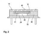
- An oscillator 10 of the present inventioncomprises a cap 11, a circuit board 40, a dielectric resonator 20, a case 30 and a stem 12.
- the cap 11, the case 30 and the stem 12should preferably have roughly the same coefficient of linear expansion as the dielectric resonator 20. They may acceptably comprise steel.
- the cap 11 and the stem 12are hermetically sealed together. Furthermore, terminal pins 13 are provided at three corners of the stem 12.
- the dielectric resonator 20comprises an electrode 22, provided on two opposite faces of a square dielectric substrate 21, and a substantially disk-like electrode removal portion 23 is provided roughly in the center of the electrode 22. Furthermore, the electrode 22 also covers the four side faces of the dielectric substrate 21, and functions as a ground.
- the dielectric resonator 20 of such a constitutionfunctions as a resonator when an electromagnetic field becomes concentrated near the substantially disk-like electrode removal portion 23.
- a concave portion 31, which the dielectric resonator 20 can fit into,is provided roughly in the center of the case 30.
- a stepprojects from the side wall of the concave portion 31 and supports part of the low face of the dielectric resonator 20. Consequently, a space is formed below the electrode removal portion 23 (FIG. 2).
- the dielectric resonator 20is stored in the concave portion 31, and should preferably be of a size such that it is able to move a certain degree in a direction parallel to the top face of the step in the concave portion 31, and does not drop into the opening.
- Through holes with screws 32 in themare provided in two adjacent side faces of the case 30 and reach as far as the inside face of the concave portion 31.
- notches 33 for holding elastic membersare provided facing the screws 32 with the dielectric resonator 20 in between them.
- Springs 34, forming elastic members,are provided in the notches, and are clasped by the side faces of the dielectric resonator 20 and the side faces of the notches 33.
- the circuit board 40comprises a stripline pattern on an insulated substrate 41, an FET 42, a chip capacitor 43, chip resistors 44a, 44b and 44c, a film-like terminal resistor 45 and a varactor diode 52.
- One end of a main line 46, comprising a striplineis connected to the gate of the FET 42, and the other end is connected to a film-like terminal resistor 45.
- the stripline 47which connects to the source of the FET 42, is connected via the chip resistor 44a to a ground electrode 48a.
- one of the striplines connecting to the drain of the FET 42is connected via the chip resistor 44b to an input terminal electrode 49.
- the input terminal electrode 49connects via the chip capacitor 43 to a ground electrode 48b.
- the other stripline connecting to the drain of the FET 42is connected via a capacitor component, comprising a gap, to an output terminal electrode 50.
- An auxiliary line 51is connected at a predetermined position via the varactor diode 52 to the ground electrode 48a. Furthermore, a stripline extracted at another position on the auxiliary line 51 connects via the chip resistor 44c to a bias terminal electrode 53. When a voltage is applied to the varactor diode 52, the capacitance of the varactor diode 52 changes, whereby the oscillating frequency of the oscillator 10 can be changed.
- the ground electrodes 48a and 48bpass through the through holes 54 and connect to ground electrodes (not shown in the diagram) provided on the rear surface of the circuit board 40.
- the ground electrodes on the rear surface of the circuit board 40are connected to the case 30 when the circuit board 40 is mounted on the case 30, thereby grounding the circuit.
- the ground electrodes on the rear surface of the circuit board 40are not provided on portions corresponding to the electrode removal portions 23 of the dielectric resonator 20, so that the striplines on the top face of the circuit board 40 can be coupled to the dielectric resonator 20.
- the case 30is provided on the stem 12, and the dielectric resonator 20 is stored inside the concave portion 31 of the case 30.
- the circuit board 40is mounted on the case 30, and the cap is hermetically sealed over it, to form the oscillator 10.
- the terminal pins 13, provided at three corners of the stem 12 and the case 30,are inserted through holes 55a, 55b and 55c, provided respectively in the input terminal electrode 49, the output terminal electrode 50 and the bias terminal electrode 53 of the circuit board 40, and connect respectively to the terminal electrodes 49, 50 and 53.
- the holes 55a, 55b and 55c, provided in the circuit board 40are the same shape as the terminal pins 13 so as to be always connected thereto.
- thermosetting adhesiveis applied in the step portion of the two-level concave portion 31 of the case 30, provided on the stem 12, and the dielectric resonator 20 is provided therein.
- Elastic membersin this case springs 34, are provided between the dielectric resonator 20 and the notches 33.
- the elastic membersare not limited to the springs 34, and may be rubber or the like.
- the circuit board 40is mounted on the case 30 and the cap is placed over it.
- a cap for adjustingis used. That is, the cap has holes at positions corresponding to the screwed through holes 32 in the case 30.
- screws 35are inserted from two directions through the holes in the cap of the oscillator, so as to touch the side faces of the dielectric resonator 20. Moreover, inserting the screws 35 applying a pressing force against the dielectric resonator 20 and alters its position. Since the screws 35 are inserted from directions intersecting at a right angle, the dielectric resonator 20 can be freely moved vertically and horizontally. The characteristics are measured each time the position of the dielectric resonator 20 is altered. In the position at which desired characteristics have been obtained, the structure is heated until the thermosetting adhesive sets, thereby fixing the dielectric resonator 20 in position. Finally, the oscillator 10 is completed by replacing the cap for adjusting with a conventional cap 11 which has no holes.
- the dielectric resonator 20may be moved using rods or the like, but it can be moved more precisely by using the screws 35. That is, the distance moved by the dielectric resonator 20 becomes more even in direct proportion to the number of rotations of the screws 35, and therefore the dielectric resonator 20 can be moved with accuracy. Furthermore, springs 34 are provided facing the screws 35, with the dielectric resonator 20 in between, thereby pushing the dielectric resonator 20 back. Therefore, the dielectric resonator 20 can be moved back by loosening the screws 35. Even without elastic members such as the springs 34, the position of the dielectric resonator 20 can be very precisely adjusted by accurately inserting the screws 35.
- the characteristicsare measured when the screws 35 and the springs 34 are touching the side faces of the dielectric resonator 20. This is because, in the dielectric resonator 20 used in the oscillator 10 of the present invention, the touching of the screws 35 and the spring 34 has no great effect on the characteristics. That is, in the dielectric resonator 20 used in the present invention, the electromagnetic field is concentrated at the disk-like electrode removal portion 23, and consequently the presence of the screws 35 and the spring 34 has almost no effect on the electromagnetic field of the dielectric resonator 20.
- this embodimentreferred to a voltage-controlled oscillator using the varactor diode 52, but the present invention is not limited to this.
- the present inventioncan be applied to an oscillator which does not use the auxiliary line 51 portion, or an oscillator which uses a gunn diode instead of the FET 42, or such like.
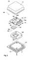
- FIG. 3is an exploded perspective view of an oscillator.
- the concave portion 31a of the case 30ahas the same width as the dielectric resonator 20 in one direction, but is wider than the dielectric resonator 20 in the other direction.
- the dielectric resonator 20can be moved in the direction in which the width of the concave portion 31a is wider.
- grooves 36running from the two opposing outside faces of the case 30a to the concave portion 31a of the case 30a, are provided. These grooves 36 enable rods or the like to be inserted to move the dielectric resonator 20.
- the holes 56a, 56b and 56c for inserting the terminal pins 13are provided on the terminals electrodes 49, 50 and 53, and are oval, being a shape formed by extending the diameter of a disk in a direction at a right angle to the direction which the dielectric resonator 20 can move in.
- the oval holes 56a, 56b and 56chave the same width as the terminal pins 13 in the direction which is at a right angle to the direction which the circuit board 40a can move in.
- the oscillatoris formed by covering it with a cap for adjusting, as in the previous embodiment.
- the cap for adjustinghas holes in its four side faces in order to move the circuit board 40a as well as the dielectric resonator 20.
- rods 37are inserted through the holes in the cap as force-applying means.
- the rods 37pass through the grooves 36 and touch the dielectric resonator 20. Since the rods 37 are inserted from opposite side faces, the dielectric resonator 20 can be freely moved in either direction.
- the circuit board 40acan be moved at a right angle to the dielectric resonator 20 by inserting the rods 37 from two side faces which are at right angles to the direction which the dielectric resonator 20 moves in.
- the dielectric resonator 20in one direction and the circuit board 40a in another direction, which is at a right angle thereto, it is possible to alter the relative positional relationship between the dielectric resonator 20 and the circuit board 40a, both horizontally and vertically.
- the capis replaced by a conventional cap with no holes to form the oscillator 10a.
- the circuit board 40ais soldered to the terminal pins 13. With such a constitution, the adjustment takes less time to perform.
- rodswere used as the force-applying means, but screws may be used instead.
- the positionwas altered by inserted the rods from two opposing side faces of the dielectric resonator and the circuit board, it is acceptable to dispense with the grooves and provide a spring between the case and the dielectric resonator, whereby the spring pushes back. This increases the number of components, but has the advantage of making adjustment less time-consuming.
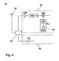
- FIG. 4shows a schematic view of the communications device of the present invention.
- the communications device 60 of the present inventioncomprises a duplexer 61, comprising a filter for transmitting and a filter for receiving, an antenna 62, which connects to a terminal for antenna connection of the duplexer 61, a circuit for transmitting 63, connected to input/output terminals of the filter for transmitting of the duplexer 61, and a circuit for receiving 64, connected to input/output terminals of the filter for receiving of the duplexer 61.
- the circuit for transmitting 63has a power amplifier (PA) for power-amplifying the transmission signal, which passes through the filter for transmitting and is emitted from the antenna 62. Furthermore, reception signal is passed from the antenna 62 through the filter for receiving, and is received by the circuit for receiving 64. After passing a low-noise amplifier (LNA) and a filter (RX) in the circuit for receiving 64, the signal is input to a mixer (MIX).
- the base oscillatoris a phase-locked loop (PLL), comprising an oscillator (VCO) and a divider (DV), and outputs a local signal to the mixer. The mixer outputs at intermediate frequency.
- the present invention described abovecomprised an adjustment mechanism for changing the relative positional relationship between the dielectric resonator and the circuit board. Consequently, when adjusting the characteristics of the oscillator, it is not necessary to remove the cap and the circuit board each time the characteristics are measured, thereby reducing the amount of time consumed when manufacturing and lowering manufacturing costs.
Landscapes
- Inductance-Capacitance Distribution Constants And Capacitance-Resistance Oscillators (AREA)
- Transceivers (AREA)
- Superheterodyne Receivers (AREA)
Abstract
Description
Claims (5)
- An oscillator (10), comprising:wherein said structure allowing movement of saiddielectric resonator (20) is a concave portion (31; 31a)larger than said dielectric resonator (20), provided in acase (30; 30a) for storing said dielectric resonator (20),the concave portion having a two-level structure forproviding a vacant portion (31; 31a) around saidelectrodeless portions (23) of said dielectric resonator(20).a dielectric resonator (20), a circuit board (40; 40a),and an adjustment mechanism for changing the relativepositional relationship of said dielectric resonator (20)and said circuit board (40; 40a);said dielectric resonator (20) comprising a dielectricsubstrate (21), electrodes (22), provided on two oppositefaces of the dielectric substrate (21), and electrodelessportions (23), provided at predetermined positions on saidsubstrate (22); andsaid adjustment mechanism comprising a structure (31; 31a)allowing movement of said dielectric resonator (20) makinguse of a force-applying means (34, 35; 37),
- The oscillator (10) according to claim 1, wherein saidstructure allows movement of said dielectric resonatormaking use of screws (35).
- The oscillator (10) according to claim 1, wherein saidstructure allows movement of said dielectric resonatormaking use of screws (35) and elastic members (34).
- The oscillator (10; 10a) according to one of claims 1 to3, wherein said structure (31; 31a) allows movement ofsaid dielectric resonator (20) in one axial directionparallel to a horizontal direction, and at a right angleto said axial direction.
- A communications device (60), comprising a circuit fortransmitting (63), a circuit for receiving (64), and anantenna (62), wherein said circuit for transmitting (63)and/or said circuit for receiving (64) comprise anoscillator (10; 10a), the oscillator (10; 10a) being theoscillator according to any one of claims 1 to 4.
Applications Claiming Priority (3)
| Application Number | Priority Date | Filing Date | Title |
|---|---|---|---|
| JP14142098 | 1998-05-22 | ||
| JP10141420AJPH11340738A (en) | 1998-05-22 | 1998-05-22 | Oscillator and communication equipment |
| EP99109968AEP0959557B1 (en) | 1998-05-22 | 1999-05-20 | Oscillator and communications device |
Related Parent Applications (1)
| Application Number | Title | Priority Date | Filing Date |
|---|---|---|---|
| EP99109968ADivisionEP0959557B1 (en) | 1998-05-22 | 1999-05-20 | Oscillator and communications device |
Publications (3)
| Publication Number | Publication Date |
|---|---|
| EP1376851A2true EP1376851A2 (en) | 2004-01-02 |
| EP1376851A3 EP1376851A3 (en) | 2004-03-10 |
| EP1376851B1 EP1376851B1 (en) | 2004-10-13 |
Family
ID=15291596
Family Applications (2)
| Application Number | Title | Priority Date | Filing Date |
|---|---|---|---|
| EP99109968AExpired - LifetimeEP0959557B1 (en) | 1998-05-22 | 1999-05-20 | Oscillator and communications device |
| EP03013983AExpired - LifetimeEP1376851B1 (en) | 1998-05-22 | 1999-05-20 | Oscillator and communications device |
Family Applications Before (1)
| Application Number | Title | Priority Date | Filing Date |
|---|---|---|---|
| EP99109968AExpired - LifetimeEP0959557B1 (en) | 1998-05-22 | 1999-05-20 | Oscillator and communications device |
Country Status (5)
| Country | Link |
|---|---|
| US (1) | US6163688A (en) |
| EP (2) | EP0959557B1 (en) |
| JP (1) | JPH11340738A (en) |
| CA (1) | CA2272224C (en) |
| DE (2) | DE69921206T2 (en) |
Cited By (5)
| Publication number | Priority date | Publication date | Assignee | Title |
|---|---|---|---|---|
| US8503962B2 (en) | 2007-06-29 | 2013-08-06 | Silicon Laboratories Inc. | Implementing a rotating harmonic rejection mixer (RHRM) for a TV tuner in an integrated circuit |
| US8538366B2 (en) | 2007-06-29 | 2013-09-17 | Silicon Laboratories Inc | Rotating harmonic rejection mixer |
| US8543077B2 (en) | 2007-06-29 | 2013-09-24 | Silicon Laboratories Inc. | Method and apparatus for controlling a harmonic rejection mixer |
| US8571512B2 (en) | 2012-01-05 | 2013-10-29 | Silicon Laboratories Inc. | Implementing a passive rotating harmonic rejection mixer (RHRM) for a TV tuner in an integrated circuit |
| DE112008001680B4 (en) | 2007-06-29 | 2019-07-11 | Silicon Laboratories Inc. | Rotating Harmonic Suppression Mixer |
Families Citing this family (5)
| Publication number | Priority date | Publication date | Assignee | Title |
|---|---|---|---|---|
| JP3914401B2 (en)* | 2001-09-06 | 2007-05-16 | 株式会社日立製作所 | Oscillator, transmission / reception module, and radar apparatus |
| JP2004032184A (en)* | 2002-06-24 | 2004-01-29 | Murata Mfg Co Ltd | High-frequency module, transmitting/receiving device and method for regulating characteristics of high-frequency module |
| US7480522B2 (en)* | 2002-12-31 | 2009-01-20 | Nokia Corporation | Rocker user interface for handheld devices, and method for implementing same |
| US20070057738A1 (en)* | 2003-07-02 | 2007-03-15 | Takahiro Baba | Oscillator device and transmission and reception device |
| CN113114111B (en)* | 2021-05-19 | 2024-07-19 | 吴国辉 | Fixing mechanism for communication equipment oscillator and use method thereof |
Family Cites Families (19)
| Publication number | Priority date | Publication date | Assignee | Title |
|---|---|---|---|---|
| JPS608651B2 (en)* | 1977-04-18 | 1985-03-05 | 株式会社日立製作所 | FET self-oscillating mixer |
| JPS6036122B2 (en)* | 1979-03-01 | 1985-08-19 | 株式会社村田製作所 | oscillator |
| JPS56138305A (en)* | 1980-03-31 | 1981-10-28 | Sanyo Electric Co Ltd | Microwave oscillator |
| JPS60140905A (en)* | 1983-12-28 | 1985-07-25 | Toshiba Corp | microwave oscillator |
| US4591806A (en)* | 1984-07-02 | 1986-05-27 | Havens Richard C | Dielectric resonator stabilized oscillator and method for optimizing the operating characteristics thereof |
| US4618836A (en)* | 1984-12-24 | 1986-10-21 | Motorola, Inc. | Wide band dielectric resonator oscillator having temperature compensation |
| US5818880A (en)* | 1990-03-30 | 1998-10-06 | Honeywell Inc. | MMIC telemetry transmitter |
| JPH04294616A (en)* | 1991-03-23 | 1992-10-19 | Fukushima Nippon Denki Kk | Voltage controlled oscillator |
| JP2800566B2 (en)* | 1991-07-23 | 1998-09-21 | 日本電気株式会社 | Field-effect transistor, high-frequency signal oscillator, and frequency conversion circuit |
| US5140285A (en)* | 1991-08-26 | 1992-08-18 | Ail Systems, Inc. | Q enhanced dielectric resonator circuit |
| JPH05152845A (en)* | 1991-11-28 | 1993-06-18 | Sanyo Electric Co Ltd | Microwave oscillator |
| JPH07122932A (en)* | 1993-10-22 | 1995-05-12 | Fujitsu Ltd | Frequency adjustment method for dielectric oscillator |
| US5768693A (en)* | 1995-02-28 | 1998-06-16 | Telecommunications Equipment Corporation | Method and apparatus for controlling frequency of a multi-channel transmitter |
| JP2708004B2 (en)* | 1995-03-20 | 1998-02-04 | 日本電気株式会社 | SHF converter |
| JPH08307119A (en)* | 1995-05-12 | 1996-11-22 | Matsushita Electric Ind Co Ltd | Method for forming electrode of dielectric resonator |
| US5578969A (en)* | 1995-06-13 | 1996-11-26 | Kain; Aron Z. | Split dielectric resonator stabilized oscillator |
| JPH0946133A (en)* | 1995-07-31 | 1997-02-14 | Matsushita Electric Ind Co Ltd | Microwave oscillator circuit and down converter using the circuit |
| FR2750816B1 (en)* | 1996-07-03 | 1998-10-23 | Matra Marconi Space France | DIELECTRIC RESONATOR SOURCE IN GALLERY MODE |
| JPH10224104A (en)* | 1997-02-05 | 1998-08-21 | Murata Mfg Co Ltd | Dielectric resonator, dielectric filter and voltage controlled oscillator using dielectric oscillator |
- 1998
- 1998-05-22JPJP10141420Apatent/JPH11340738A/enactivePending
- 1999
- 1999-05-19CACA002272224Apatent/CA2272224C/ennot_activeExpired - Fee Related
- 1999-05-20EPEP99109968Apatent/EP0959557B1/ennot_activeExpired - Lifetime
- 1999-05-20DEDE69921206Tpatent/DE69921206T2/ennot_activeExpired - Fee Related
- 1999-05-20DEDE69911498Tpatent/DE69911498T2/ennot_activeExpired - Fee Related
- 1999-05-20EPEP03013983Apatent/EP1376851B1/ennot_activeExpired - Lifetime
- 1999-05-20USUS09/315,737patent/US6163688A/ennot_activeExpired - Fee Related
Cited By (7)
| Publication number | Priority date | Publication date | Assignee | Title |
|---|---|---|---|---|
| US8503962B2 (en) | 2007-06-29 | 2013-08-06 | Silicon Laboratories Inc. | Implementing a rotating harmonic rejection mixer (RHRM) for a TV tuner in an integrated circuit |
| US8538366B2 (en) | 2007-06-29 | 2013-09-17 | Silicon Laboratories Inc | Rotating harmonic rejection mixer |
| US8543077B2 (en) | 2007-06-29 | 2013-09-24 | Silicon Laboratories Inc. | Method and apparatus for controlling a harmonic rejection mixer |
| US8768281B2 (en) | 2007-06-29 | 2014-07-01 | Silicon Laboratories Inc. | Method and apparatus for controlling a harmonic rejection mixer |
| US8774750B2 (en) | 2007-06-29 | 2014-07-08 | Silicon Laboratories Inc. | Method and apparatus for controlling a harmonic rejection mixer |
| DE112008001680B4 (en) | 2007-06-29 | 2019-07-11 | Silicon Laboratories Inc. | Rotating Harmonic Suppression Mixer |
| US8571512B2 (en) | 2012-01-05 | 2013-10-29 | Silicon Laboratories Inc. | Implementing a passive rotating harmonic rejection mixer (RHRM) for a TV tuner in an integrated circuit |
Also Published As
| Publication number | Publication date |
|---|---|
| DE69911498T2 (en) | 2004-07-01 |
| US6163688A (en) | 2000-12-19 |
| EP1376851A3 (en) | 2004-03-10 |
| EP0959557A1 (en) | 1999-11-24 |
| CA2272224A1 (en) | 1999-11-22 |
| EP0959557B1 (en) | 2003-09-24 |
| DE69921206D1 (en) | 2004-11-18 |
| JPH11340738A (en) | 1999-12-10 |
| DE69921206T2 (en) | 2005-11-03 |
| DE69911498D1 (en) | 2003-10-30 |
| CA2272224C (en) | 2002-07-09 |
| EP1376851B1 (en) | 2004-10-13 |
Similar Documents
| Publication | Publication Date | Title |
|---|---|---|
| US6825734B2 (en) | Oscillator module incorporating spiral looped-stub resonator | |
| CN1983711A (en) | Electronically tunable dielectric resonator circuits | |
| EP1376851B1 (en) | Oscillator and communications device | |
| US5321374A (en) | Transverse electromagnetic mode resonator | |
| JP3087664B2 (en) | Dielectric resonator device and high frequency module | |
| US6204739B1 (en) | Dielectric resonant apparatus | |
| US7394334B2 (en) | Dielectric resonance apparatus, oscillation apparatus, and transmission/reception apparatus | |
| JP2000261234A (en) | Plate radiation type oscillation device | |
| US4871983A (en) | Electronically tuned dielectric resonator stabilized oscillator | |
| US6891452B2 (en) | High-frequency circuit device and transmitter/receiver | |
| KR100394811B1 (en) | High-frequency circuit module, filter, duplexer, and communication device | |
| CA2272219C (en) | Oscillator and communications device | |
| JP2000059114A (en) | Frequency adjustment device for NRD guide millimeter wave band oscillator | |
| US5357218A (en) | Self-shielding microstrip assembly | |
| US6369676B2 (en) | High-frequency module | |
| JPH04294616A (en) | Voltage controlled oscillator | |
| US6531934B1 (en) | Dielectric resonator, dielectric filter, dielectric duplexer, oscillator, and communication device | |
| US5734307A (en) | Distributed device for differential circuit | |
| US20080036548A1 (en) | Resonator For A Voltage Controlled Oscillator And Manufacturing Method Thereof | |
| US4097822A (en) | Broad-band cavity-tuned transistor oscillator | |
| Katz et al. | Adjustable Reflective Predistortion Circuit | |
| JPH11340737A (en) | Dielectric oscillator | |
| JPH11234009A (en) | Oscillator device | |
| JPS61196604A (en) | Microwave oscillator | |
| JP2002299954A (en) | Voltage controlled oscillator and electronic device using the same |
Legal Events
| Date | Code | Title | Description |
|---|---|---|---|
| PUAI | Public reference made under article 153(3) epc to a published international application that has entered the european phase | Free format text:ORIGINAL CODE: 0009012 | |
| 17P | Request for examination filed | Effective date:20030620 | |
| AC | Divisional application: reference to earlier application | Ref document number:0959557 Country of ref document:EP Kind code of ref document:P | |
| AK | Designated contracting states | Kind code of ref document:A2 Designated state(s):DE FI FR SE | |
| PUAL | Search report despatched | Free format text:ORIGINAL CODE: 0009013 | |
| AK | Designated contracting states | Kind code of ref document:A3 Designated state(s):DE FI FR SE | |
| GRAP | Despatch of communication of intention to grant a patent | Free format text:ORIGINAL CODE: EPIDOSNIGR1 | |
| GRAS | Grant fee paid | Free format text:ORIGINAL CODE: EPIDOSNIGR3 | |
| GRAA | (expected) grant | Free format text:ORIGINAL CODE: 0009210 | |
| AC | Divisional application: reference to earlier application | Ref document number:0959557 Country of ref document:EP Kind code of ref document:P | |
| AK | Designated contracting states | Kind code of ref document:B1 Designated state(s):DE FI FR SE | |
| PG25 | Lapsed in a contracting state [announced via postgrant information from national office to epo] | Ref country code:FI Free format text:LAPSE BECAUSE OF FAILURE TO SUBMIT A TRANSLATION OF THE DESCRIPTION OR TO PAY THE FEE WITHIN THE PRESCRIBED TIME-LIMIT Effective date:20041013 | |
| REF | Corresponds to: | Ref document number:69921206 Country of ref document:DE Date of ref document:20041118 Kind code of ref document:P | |
| AKX | Designation fees paid | Designated state(s):DE FI FR SE | |
| PG25 | Lapsed in a contracting state [announced via postgrant information from national office to epo] | Ref country code:SE Free format text:LAPSE BECAUSE OF FAILURE TO SUBMIT A TRANSLATION OF THE DESCRIPTION OR TO PAY THE FEE WITHIN THE PRESCRIBED TIME-LIMIT Effective date:20050113 | |
| PLBE | No opposition filed within time limit | Free format text:ORIGINAL CODE: 0009261 | |
| STAA | Information on the status of an ep patent application or granted ep patent | Free format text:STATUS: NO OPPOSITION FILED WITHIN TIME LIMIT | |
| ET | Fr: translation filed | ||
| 26N | No opposition filed | Effective date:20050714 | |
| PGFP | Annual fee paid to national office [announced via postgrant information from national office to epo] | Ref country code:DE Payment date:20070517 Year of fee payment:9 | |
| PG25 | Lapsed in a contracting state [announced via postgrant information from national office to epo] | Ref country code:DE Free format text:LAPSE BECAUSE OF NON-PAYMENT OF DUE FEES Effective date:20081202 | |
| REG | Reference to a national code | Ref country code:FR Ref legal event code:ST Effective date:20100129 | |
| PG25 | Lapsed in a contracting state [announced via postgrant information from national office to epo] | Ref country code:FR Free format text:LAPSE BECAUSE OF NON-PAYMENT OF DUE FEES Effective date:20090602 | |
| PGFP | Annual fee paid to national office [announced via postgrant information from national office to epo] | Ref country code:FR Payment date:20080514 Year of fee payment:10 |