EP1376717A2 - Method of manufacturing organic el element, organic el element, and organic el display device - Google Patents
Method of manufacturing organic el element, organic el element, and organic el display deviceDownload PDFInfo
- Publication number
- EP1376717A2 EP1376717A2EP03077510AEP03077510AEP1376717A2EP 1376717 A2EP1376717 A2EP 1376717A2EP 03077510 AEP03077510 AEP 03077510AEP 03077510 AEP03077510 AEP 03077510AEP 1376717 A2EP1376717 A2EP 1376717A2
- Authority
- EP
- European Patent Office
- Prior art keywords
- organic
- luminescent
- manufacturing
- luminescent layer
- layer
- Prior art date
- Legal status (The legal status is an assumption and is not a legal conclusion. Google has not performed a legal analysis and makes no representation as to the accuracy of the status listed.)
- Withdrawn
Links
- 238000004519manufacturing processMethods0.000titleclaimsabstractdescription64
- 238000000034methodMethods0.000claimsabstractdescription117
- 150000002894organic compoundsChemical class0.000claimsabstractdescription38
- 239000000758substrateSubstances0.000claimsabstractdescription35
- 238000000059patterningMethods0.000claimsabstractdescription20
- 239000000463materialSubstances0.000claimsdescription96
- 238000002347injectionMethods0.000claimsdescription70
- 239000007924injectionSubstances0.000claimsdescription70
- 238000012546transferMethods0.000claimsdescription70
- 239000000203mixtureSubstances0.000claimsdescription51
- 238000004020luminiscence typeMethods0.000claimsdescription31
- 229920000642polymerPolymers0.000claimsdescription25
- 239000003086colorantSubstances0.000claimsdescription23
- 238000001771vacuum depositionMethods0.000claimsdescription22
- 230000015572biosynthetic processEffects0.000claimsdescription13
- 239000007788liquidSubstances0.000claimsdescription12
- 238000007599dischargingMethods0.000claimsdescription9
- 230000001681protective effectEffects0.000claimsdescription9
- 150000001875compoundsChemical class0.000claimsdescription8
- -1polyparaphenylene vinylenePolymers0.000claimsdescription8
- 238000000638solvent extractionMethods0.000claimsdescription5
- 229920001577copolymerPolymers0.000claimsdescription4
- 230000027756respiratory electron transport chainEffects0.000claimsdescription4
- 238000013461designMethods0.000abstractdescription5
- 238000005457optimizationMethods0.000abstractdescription2
- 239000010410layerSubstances0.000description223
- 239000010408filmSubstances0.000description31
- 239000007850fluorescent dyeSubstances0.000description26
- 239000010409thin filmSubstances0.000description19
- 238000000576coating methodMethods0.000description12
- 239000002243precursorSubstances0.000description12
- 229920003227poly(N-vinyl carbazole)Polymers0.000description11
- 229920000553poly(phenylenevinylene)Polymers0.000description11
- 239000011159matrix materialSubstances0.000description10
- 229910052751metalInorganic materials0.000description10
- 239000002184metalSubstances0.000description10
- 239000011521glassSubstances0.000description8
- 238000000206photolithographyMethods0.000description8
- 229910052782aluminiumInorganic materials0.000description7
- 238000000151depositionMethods0.000description7
- 238000010438heat treatmentMethods0.000description7
- XAGFODPZIPBFFR-UHFFFAOYSA-NaluminiumChemical compound[Al]XAGFODPZIPBFFR-UHFFFAOYSA-N0.000description6
- 239000011248coating agentSubstances0.000description6
- 238000004528spin coatingMethods0.000description6
- 238000007611bar coating methodMethods0.000description5
- 238000005266castingMethods0.000description5
- 238000007598dipping methodMethods0.000description5
- 230000007261regionalizationEffects0.000description5
- 239000002904solventSubstances0.000description5
- 238000003860storageMethods0.000description5
- 238000010586diagramMethods0.000description4
- 239000011261inert gasSubstances0.000description4
- 239000012299nitrogen atmosphereSubstances0.000description4
- PYWVYCXTNDRMGF-UHFFFAOYSA-Nrhodamine BChemical compound[Cl-].C=12C=CC(=[N+](CC)CC)C=C2OC2=CC(N(CC)CC)=CC=C2C=1C1=CC=CC=C1C(O)=OPYWVYCXTNDRMGF-UHFFFAOYSA-N0.000description4
- KLCLIOISYBHYDZ-UHFFFAOYSA-N1,4,4-triphenylbuta-1,3-dienylbenzeneChemical compoundC=1C=CC=CC=1C(C=1C=CC=CC=1)=CC=C(C=1C=CC=CC=1)C1=CC=CC=C1KLCLIOISYBHYDZ-UHFFFAOYSA-N0.000description3
- 239000000969carrierSubstances0.000description3
- 238000004040coloringMethods0.000description3
- 238000010276constructionMethods0.000description3
- 230000007547defectEffects0.000description3
- 238000011156evaluationMethods0.000description3
- 230000002349favourable effectEffects0.000description3
- 238000002156mixingMethods0.000description3
- 229920000620organic polymerPolymers0.000description3
- 230000002093peripheral effectEffects0.000description3
- 230000008569processEffects0.000description3
- 238000004544sputter depositionMethods0.000description3
- XLYOFNOQVPJJNP-UHFFFAOYSA-NwaterSubstancesOXLYOFNOQVPJJNP-UHFFFAOYSA-N0.000description3
- 239000004925Acrylic resinSubstances0.000description2
- 229920000178Acrylic resinPolymers0.000description2
- XKRFYHLGVUSROY-UHFFFAOYSA-NArgonChemical compound[Ar]XKRFYHLGVUSROY-UHFFFAOYSA-N0.000description2
- 239000004642PolyimideSubstances0.000description2
- NRCMAYZCPIVABH-UHFFFAOYSA-NQuinacridoneChemical compoundN1C2=CC=CC=C2C(=O)C2=C1C=C1C(=O)C3=CC=CC=C3NC1=C2NRCMAYZCPIVABH-UHFFFAOYSA-N0.000description2
- XLOMVQKBTHCTTD-UHFFFAOYSA-NZinc monoxideChemical compound[Zn]=OXLOMVQKBTHCTTD-UHFFFAOYSA-N0.000description2
- 238000010521absorption reactionMethods0.000description2
- 230000008859changeEffects0.000description2
- 238000004140cleaningMethods0.000description2
- 229920000547conjugated polymerPolymers0.000description2
- 230000021615conjugationEffects0.000description2
- 239000000470constituentSubstances0.000description2
- ZYGHJZDHTFUPRJ-UHFFFAOYSA-NcoumarinChemical compoundC1=CC=C2OC(=O)C=CC2=C1ZYGHJZDHTFUPRJ-UHFFFAOYSA-N0.000description2
- 238000009510drug designMethods0.000description2
- 239000003822epoxy resinSubstances0.000description2
- 238000010030laminatingMethods0.000description2
- 230000031700light absorptionEffects0.000description2
- 230000005499meniscusEffects0.000description2
- 125000002080perylenyl groupChemical groupC1(=CC=C2C=CC=C3C4=CC=CC5=CC=CC(C1=C23)=C45)*0.000description2
- CSHWQDPOILHKBI-UHFFFAOYSA-NperyreneNatural productsC1=CC(C2=CC=CC=3C2=C2C=CC=3)=C3C2=CC=CC3=C1CSHWQDPOILHKBI-UHFFFAOYSA-N0.000description2
- 229920000647polyepoxidePolymers0.000description2
- 229920001721polyimidePolymers0.000description2
- 235000019353potassium silicateNutrition0.000description2
- 150000003219pyrazolinesChemical class0.000description2
- 230000002940repellentEffects0.000description2
- 239000005871repellentSubstances0.000description2
- YYMBJDOZVAITBP-UHFFFAOYSA-NrubreneChemical compoundC1=CC=CC=C1C(C1=C(C=2C=CC=CC=2)C2=CC=CC=C2C(C=2C=CC=CC=2)=C11)=C(C=CC=C2)C2=C1C1=CC=CC=C1YYMBJDOZVAITBP-UHFFFAOYSA-N0.000description2
- 229910052709silverInorganic materials0.000description2
- 239000007787solidSubstances0.000description2
- 230000003068static effectEffects0.000description2
- DTZWGKCFKSJGPK-VOTSOKGWSA-N(e)-2-(2-methyl-6-(2-(1,1,7,7-tetramethyl-1,2,3,5,6,7-hexahydropyrido[3,2,1-ij]quinolin-9-yl)vinyl)-4h-pyran-4-ylidene)malononitrileChemical compoundO1C(C)=CC(=C(C#N)C#N)C=C1\C=C\C1=CC(C(CCN2CCC3(C)C)(C)C)=C2C3=C1DTZWGKCFKSJGPK-VOTSOKGWSA-N0.000description1
- SLLFVLKNXABYGI-UHFFFAOYSA-N1,2,3-benzoxadiazoleChemical compoundC1=CC=C2ON=NC2=C1SLLFVLKNXABYGI-UHFFFAOYSA-N0.000description1
- UHXOHPVVEHBKKT-UHFFFAOYSA-N1-(2,2-diphenylethenyl)-4-[4-(2,2-diphenylethenyl)phenyl]benzeneChemical compoundC=1C=C(C=2C=CC(C=C(C=3C=CC=CC=3)C=3C=CC=CC=3)=CC=2)C=CC=1C=C(C=1C=CC=CC=1)C1=CC=CC=C1UHXOHPVVEHBKKT-UHFFFAOYSA-N0.000description1
- ZMLPKJYZRQZLDA-UHFFFAOYSA-N1-(2-phenylethenyl)-4-[4-(2-phenylethenyl)phenyl]benzeneChemical groupC=1C=CC=CC=1C=CC(C=C1)=CC=C1C(C=C1)=CC=C1C=CC1=CC=CC=C1ZMLPKJYZRQZLDA-UHFFFAOYSA-N0.000description1
- DZNJMLVCIZGWSC-UHFFFAOYSA-N3',6'-bis(diethylamino)spiro[2-benzofuran-3,9'-xanthene]-1-oneChemical compoundO1C(=O)C2=CC=CC=C2C21C1=CC=C(N(CC)CC)C=C1OC1=CC(N(CC)CC)=CC=C21DZNJMLVCIZGWSC-UHFFFAOYSA-N0.000description1
- GOLORTLGFDVFDW-UHFFFAOYSA-N3-(1h-benzimidazol-2-yl)-7-(diethylamino)chromen-2-oneChemical compoundC1=CC=C2NC(C3=CC4=CC=C(C=C4OC3=O)N(CC)CC)=NC2=C1GOLORTLGFDVFDW-UHFFFAOYSA-N0.000description1
- NSPMIYGKQJPBQR-UHFFFAOYSA-N4H-1,2,4-triazoleChemical classC=1N=CNN=1NSPMIYGKQJPBQR-UHFFFAOYSA-N0.000description1
- KQFZOWUXULRDDS-UHFFFAOYSA-N4h-quinolizine-1-carboxylic acidChemical compoundC1=CC=CN2CC=CC(C(=O)O)=C21KQFZOWUXULRDDS-UHFFFAOYSA-N0.000description1
- RIUSGHALMCFISX-UHFFFAOYSA-N7-(dimethylamino)-2,3-dihydro-1h-cyclopenta[c]chromen-4-oneChemical compoundO=C1OC2=CC(N(C)C)=CC=C2C2=C1CCC2RIUSGHALMCFISX-UHFFFAOYSA-N0.000description1
- GZEYLLPOQRZUDF-UHFFFAOYSA-N7-(dimethylamino)-4-methylchromen-2-oneChemical compoundCC1=CC(=O)OC2=CC(N(C)C)=CC=C21GZEYLLPOQRZUDF-UHFFFAOYSA-N0.000description1
- 229910001148Al-Li alloyInorganic materials0.000description1
- 229910052693EuropiumInorganic materials0.000description1
- 229920000265PolyparaphenylenePolymers0.000description1
- BQCADISMDOOEFD-UHFFFAOYSA-NSilverChemical compound[Ag]BQCADISMDOOEFD-UHFFFAOYSA-N0.000description1
- DGEZNRSVGBDHLK-UHFFFAOYSA-N[1,10]phenanthrolineChemical compoundC1=CN=C2C3=NC=CC=C3C=CC2=C1DGEZNRSVGBDHLK-UHFFFAOYSA-N0.000description1
- 229910052783alkali metalInorganic materials0.000description1
- 150000001340alkali metalsChemical class0.000description1
- 229910052784alkaline earth metalInorganic materials0.000description1
- 239000000956alloySubstances0.000description1
- 229910045601alloyInorganic materials0.000description1
- 150000001454anthracenesChemical class0.000description1
- 239000007864aqueous solutionSubstances0.000description1
- 229910052786argonInorganic materials0.000description1
- 150000004984aromatic diaminesChemical class0.000description1
- 125000003118aryl groupChemical group0.000description1
- 239000012298atmosphereSubstances0.000description1
- 239000002585baseSubstances0.000description1
- 230000008033biological extinctionEffects0.000description1
- 239000006229carbon blackSubstances0.000description1
- VYXSBFYARXAAKO-WTKGSRSZSA-Nchembl402140Chemical compoundCl.C1=2C=C(C)C(NCC)=CC=2OC2=C\C(=N/CC)C(C)=CC2=C1C1=CC=CC=C1C(=O)OCCVYXSBFYARXAAKO-WTKGSRSZSA-N0.000description1
- CHZWRIFDYXSVOD-UHFFFAOYSA-Mchromenylium;perchlorateChemical compound[O-]Cl(=O)(=O)=O.[O+]1=CC=CC2=CC=CC=C21CHZWRIFDYXSVOD-UHFFFAOYSA-M0.000description1
- 238000004891communicationMethods0.000description1
- 239000002131composite materialSubstances0.000description1
- 229920001940conductive polymerPolymers0.000description1
- 230000001268conjugating effectEffects0.000description1
- 238000011109contaminationMethods0.000description1
- 229960000956coumarinDrugs0.000description1
- 235000001671coumarinNutrition0.000description1
- GLNDAGDHSLMOKX-UHFFFAOYSA-Ncoumarin 120Chemical compoundC1=C(N)C=CC2=C1OC(=O)C=C2CGLNDAGDHSLMOKX-UHFFFAOYSA-N0.000description1
- KDTAEYOYAZPLIC-UHFFFAOYSA-Ncoumarin 152Chemical compoundFC(F)(F)C1=CC(=O)OC2=CC(N(C)C)=CC=C21KDTAEYOYAZPLIC-UHFFFAOYSA-N0.000description1
- VSSSHNJONFTXHS-UHFFFAOYSA-Ncoumarin 153Chemical compoundC12=C3CCCN2CCCC1=CC1=C3OC(=O)C=C1C(F)(F)FVSSSHNJONFTXHS-UHFFFAOYSA-N0.000description1
- JBPCDMSEJVCNGV-UHFFFAOYSA-Ncoumarin 334Chemical compoundC1CCC2=C(OC(C(C(=O)C)=C3)=O)C3=CC3=C2N1CCC3JBPCDMSEJVCNGV-UHFFFAOYSA-N0.000description1
- LGDDFMCJIHJNMK-UHFFFAOYSA-Ncoumarin 337Chemical compoundC12=C3CCCN2CCCC1=CC1=C3OC(=O)C(C#N)=C1LGDDFMCJIHJNMK-UHFFFAOYSA-N0.000description1
- KCDCNGXPPGQERR-UHFFFAOYSA-Ncoumarin 343Chemical compoundC1CCC2=C(OC(C(C(=O)O)=C3)=O)C3=CC3=C2N1CCC3KCDCNGXPPGQERR-UHFFFAOYSA-N0.000description1
- AFYCEAFSNDLKSX-UHFFFAOYSA-Ncoumarin 460Chemical compoundCC1=CC(=O)OC2=CC(N(CC)CC)=CC=C21AFYCEAFSNDLKSX-UHFFFAOYSA-N0.000description1
- VMJKUPWQKZFFCX-UHFFFAOYSA-Ncoumarin 504Chemical compoundC1CCC2=C(OC(C(C(=O)OCC)=C3)=O)C3=CC3=C2N1CCC3VMJKUPWQKZFFCX-UHFFFAOYSA-N0.000description1
- VBVAVBCYMYWNOU-UHFFFAOYSA-Ncoumarin 6Chemical compoundC1=CC=C2SC(C3=CC4=CC=C(C=C4OC3=O)N(CC)CC)=NC2=C1VBVAVBCYMYWNOU-UHFFFAOYSA-N0.000description1
- 150000004775coumarinsChemical class0.000description1
- 230000008878couplingEffects0.000description1
- 238000010168coupling processMethods0.000description1
- 238000005859coupling reactionMethods0.000description1
- 230000009849deactivationEffects0.000description1
- 230000006866deteriorationEffects0.000description1
- 239000002019doping agentSubstances0.000description1
- 230000007613environmental effectEffects0.000description1
- 125000005678ethenylene groupChemical group[H]C([*:1])=C([H])[*:2]0.000description1
- OGPBJKLSAFTDLK-UHFFFAOYSA-Neuropium atomChemical compound[Eu]OGPBJKLSAFTDLK-UHFFFAOYSA-N0.000description1
- 238000002474experimental methodMethods0.000description1
- 239000007789gasSubstances0.000description1
- RBTKNAXYKSUFRK-UHFFFAOYSA-Nheliogen blueChemical compound[Cu].[N-]1C2=C(C=CC=C3)C3=C1N=C([N-]1)C3=CC=CC=C3C1=NC([N-]1)=C(C=CC=C3)C3=C1N=C([N-]1)C3=CC=CC=C3C1=N2RBTKNAXYKSUFRK-UHFFFAOYSA-N0.000description1
- 238000005470impregnationMethods0.000description1
- 230000006872improvementEffects0.000description1
- 229910003437indium oxideInorganic materials0.000description1
- PJXISJQVUVHSOJ-UHFFFAOYSA-Nindium(iii) oxideChemical compound[O-2].[O-2].[O-2].[In+3].[In+3]PJXISJQVUVHSOJ-UHFFFAOYSA-N0.000description1
- AMGQUBHHOARCQH-UHFFFAOYSA-Nindium;oxotinChemical compound[In].[Sn]=OAMGQUBHHOARCQH-UHFFFAOYSA-N0.000description1
- 229910010272inorganic materialInorganic materials0.000description1
- 239000011147inorganic materialSubstances0.000description1
- 230000003993interactionEffects0.000description1
- 238000003475laminationMethods0.000description1
- 238000003698laser cuttingMethods0.000description1
- 239000000990laser dyeSubstances0.000description1
- 239000002346layers by functionSubstances0.000description1
- 229910052744lithiumInorganic materials0.000description1
- 238000001748luminescence spectrumMethods0.000description1
- 229910052749magnesiumInorganic materials0.000description1
- 230000000873masking effectEffects0.000description1
- 150000002739metalsChemical class0.000description1
- 230000003287optical effectEffects0.000description1
- 239000012044organic layerSubstances0.000description1
- 239000011368organic materialSubstances0.000description1
- 239000003960organic solventSubstances0.000description1
- 150000004866oxadiazolesChemical class0.000description1
- JZRYQZJSTWVBBD-UHFFFAOYSA-Npentaporphyrin iChemical compoundN1C(C=C2NC(=CC3=NC(=C4)C=C3)C=C2)=CC=C1C=C1C=CC4=N1JZRYQZJSTWVBBD-UHFFFAOYSA-N0.000description1
- 230000035699permeabilityEffects0.000description1
- IEQIEDJGQAUEQZ-UHFFFAOYSA-NphthalocyanineChemical compoundN1C(N=C2C3=CC=CC=C3C(N=C3C4=CC=CC=C4C(=N4)N3)=N2)=C(C=CC=C2)C2=C1N=C1C2=CC=CC=C2C4=N1IEQIEDJGQAUEQZ-UHFFFAOYSA-N0.000description1
- 229920003023plasticPolymers0.000description1
- 229920000503poly(2,5-furylene vinylene) polymerPolymers0.000description1
- 229920000767polyanilinePolymers0.000description1
- RKCAIXNGYQCCAL-UHFFFAOYSA-NporphinChemical compoundN1C(C=C2N=C(C=C3NC(=C4)C=C3)C=C2)=CC=C1C=C1C=CC4=N1RKCAIXNGYQCCAL-UHFFFAOYSA-N0.000description1
- 238000001556precipitationMethods0.000description1
- 230000002265preventionEffects0.000description1
- 238000007639printingMethods0.000description1
- 238000010791quenchingMethods0.000description1
- 230000000171quenching effectEffects0.000description1
- 238000005215recombinationMethods0.000description1
- 230000006798recombinationEffects0.000description1
- 239000011347resinSubstances0.000description1
- 229920005989resinPolymers0.000description1
- 230000004044responseEffects0.000description1
- DJWWHVKRLDNDJK-UHFFFAOYSA-Nrhodamine 640 perchlorateChemical compound[O-]Cl(=O)(=O)=O.OC(=O)C1=CC=CC=C1C(C1=CC=2CCCN3CCCC(C=23)=C1O1)=C2C1=C(CCC1)C3=[N+]1CCCC3=C2DJWWHVKRLDNDJK-UHFFFAOYSA-N0.000description1
- 229940043267rhodamine bDrugs0.000description1
- 238000007789sealingMethods0.000description1
- 239000004332silverSubstances0.000description1
- 238000001228spectrumMethods0.000description1
- 230000006641stabilisationEffects0.000description1
- 238000011105stabilizationMethods0.000description1
- 239000010935stainless steelSubstances0.000description1
- 229910001220stainless steelInorganic materials0.000description1
- 238000004381surface treatmentMethods0.000description1
- 229920001187thermosetting polymerPolymers0.000description1
- XOLBLPGZBRYERU-UHFFFAOYSA-Ntin dioxideChemical compoundO=[Sn]=OXOLBLPGZBRYERU-UHFFFAOYSA-N0.000description1
- 229910001887tin oxideInorganic materials0.000description1
- JFLKFZNIIQFQBS-FNCQTZNRSA-Ntrans,trans-1,4-Diphenyl-1,3-butadieneChemical groupC=1C=CC=CC=1\C=C\C=C\C1=CC=CC=C1JFLKFZNIIQFQBS-FNCQTZNRSA-N0.000description1
- 150000003852triazolesChemical class0.000description1
- 239000002699waste materialSubstances0.000description1
- 239000011787zinc oxideSubstances0.000description1
Images


Classifications
- H—ELECTRICITY
- H05—ELECTRIC TECHNIQUES NOT OTHERWISE PROVIDED FOR
- H05B—ELECTRIC HEATING; ELECTRIC LIGHT SOURCES NOT OTHERWISE PROVIDED FOR; CIRCUIT ARRANGEMENTS FOR ELECTRIC LIGHT SOURCES, IN GENERAL
- H05B33/00—Electroluminescent light sources
- H05B33/10—Apparatus or processes specially adapted to the manufacture of electroluminescent light sources
- H—ELECTRICITY
- H10—SEMICONDUCTOR DEVICES; ELECTRIC SOLID-STATE DEVICES NOT OTHERWISE PROVIDED FOR
- H10K—ORGANIC ELECTRIC SOLID-STATE DEVICES
- H10K50/00—Organic light-emitting devices
- H10K50/80—Constructional details
- H10K50/84—Passivation; Containers; Encapsulations
- H10K50/842—Containers
- H10K50/8426—Peripheral sealing arrangements, e.g. adhesives, sealants
- H—ELECTRICITY
- H10—SEMICONDUCTOR DEVICES; ELECTRIC SOLID-STATE DEVICES NOT OTHERWISE PROVIDED FOR
- H10K—ORGANIC ELECTRIC SOLID-STATE DEVICES
- H10K50/00—Organic light-emitting devices
- H10K50/80—Constructional details
- H10K50/84—Passivation; Containers; Encapsulations
- H10K50/844—Encapsulations
- H—ELECTRICITY
- H10—SEMICONDUCTOR DEVICES; ELECTRIC SOLID-STATE DEVICES NOT OTHERWISE PROVIDED FOR
- H10K—ORGANIC ELECTRIC SOLID-STATE DEVICES
- H10K59/00—Integrated devices, or assemblies of multiple devices, comprising at least one organic light-emitting element covered by group H10K50/00
- H10K59/30—Devices specially adapted for multicolour light emission
- H10K59/35—Devices specially adapted for multicolour light emission comprising red-green-blue [RGB] subpixels
- H—ELECTRICITY
- H10—SEMICONDUCTOR DEVICES; ELECTRIC SOLID-STATE DEVICES NOT OTHERWISE PROVIDED FOR
- H10K—ORGANIC ELECTRIC SOLID-STATE DEVICES
- H10K59/00—Integrated devices, or assemblies of multiple devices, comprising at least one organic light-emitting element covered by group H10K50/00
- H10K59/80—Constructional details
- H10K59/87—Passivation; Containers; Encapsulations
- H10K59/873—Encapsulations
- C—CHEMISTRY; METALLURGY
- C09—DYES; PAINTS; POLISHES; NATURAL RESINS; ADHESIVES; COMPOSITIONS NOT OTHERWISE PROVIDED FOR; APPLICATIONS OF MATERIALS NOT OTHERWISE PROVIDED FOR
- C09K—MATERIALS FOR MISCELLANEOUS APPLICATIONS, NOT PROVIDED FOR ELSEWHERE
- C09K2323/00—Functional layers of liquid crystal optical display excluding electroactive liquid crystal layer characterised by chemical composition
- H—ELECTRICITY
- H10—SEMICONDUCTOR DEVICES; ELECTRIC SOLID-STATE DEVICES NOT OTHERWISE PROVIDED FOR
- H10K—ORGANIC ELECTRIC SOLID-STATE DEVICES
- H10K50/00—Organic light-emitting devices
- H10K50/80—Constructional details
- H10K50/86—Arrangements for improving contrast, e.g. preventing reflection of ambient light
- H10K50/865—Arrangements for improving contrast, e.g. preventing reflection of ambient light comprising light absorbing layers, e.g. light-blocking layers
- H—ELECTRICITY
- H10—SEMICONDUCTOR DEVICES; ELECTRIC SOLID-STATE DEVICES NOT OTHERWISE PROVIDED FOR
- H10K—ORGANIC ELECTRIC SOLID-STATE DEVICES
- H10K59/00—Integrated devices, or assemblies of multiple devices, comprising at least one organic light-emitting element covered by group H10K50/00
- H10K59/10—OLED displays
- H10K59/12—Active-matrix OLED [AMOLED] displays
- H—ELECTRICITY
- H10—SEMICONDUCTOR DEVICES; ELECTRIC SOLID-STATE DEVICES NOT OTHERWISE PROVIDED FOR
- H10K—ORGANIC ELECTRIC SOLID-STATE DEVICES
- H10K59/00—Integrated devices, or assemblies of multiple devices, comprising at least one organic light-emitting element covered by group H10K50/00
- H10K59/10—OLED displays
- H10K59/17—Passive-matrix OLED displays
- H10K59/173—Passive-matrix OLED displays comprising banks or shadow masks
- H—ELECTRICITY
- H10—SEMICONDUCTOR DEVICES; ELECTRIC SOLID-STATE DEVICES NOT OTHERWISE PROVIDED FOR
- H10K—ORGANIC ELECTRIC SOLID-STATE DEVICES
- H10K59/00—Integrated devices, or assemblies of multiple devices, comprising at least one organic light-emitting element covered by group H10K50/00
- H10K59/30—Devices specially adapted for multicolour light emission
- H10K59/35—Devices specially adapted for multicolour light emission comprising red-green-blue [RGB] subpixels
- H10K59/353—Devices specially adapted for multicolour light emission comprising red-green-blue [RGB] subpixels characterised by the geometrical arrangement of the RGB subpixels
- H—ELECTRICITY
- H10—SEMICONDUCTOR DEVICES; ELECTRIC SOLID-STATE DEVICES NOT OTHERWISE PROVIDED FOR
- H10K—ORGANIC ELECTRIC SOLID-STATE DEVICES
- H10K59/00—Integrated devices, or assemblies of multiple devices, comprising at least one organic light-emitting element covered by group H10K50/00
- H10K59/80—Constructional details
- H10K59/87—Passivation; Containers; Encapsulations
- H10K59/871—Self-supporting sealing arrangements
- H10K59/8722—Peripheral sealing arrangements, e.g. adhesives, sealants
- H—ELECTRICITY
- H10—SEMICONDUCTOR DEVICES; ELECTRIC SOLID-STATE DEVICES NOT OTHERWISE PROVIDED FOR
- H10K—ORGANIC ELECTRIC SOLID-STATE DEVICES
- H10K59/00—Integrated devices, or assemblies of multiple devices, comprising at least one organic light-emitting element covered by group H10K50/00
- H10K59/80—Constructional details
- H10K59/8791—Arrangements for improving contrast, e.g. preventing reflection of ambient light
- H10K59/8792—Arrangements for improving contrast, e.g. preventing reflection of ambient light comprising light absorbing layers, e.g. black layers
- H—ELECTRICITY
- H10—SEMICONDUCTOR DEVICES; ELECTRIC SOLID-STATE DEVICES NOT OTHERWISE PROVIDED FOR
- H10K—ORGANIC ELECTRIC SOLID-STATE DEVICES
- H10K71/00—Manufacture or treatment specially adapted for the organic devices covered by this subclass
- H—ELECTRICITY
- H10—SEMICONDUCTOR DEVICES; ELECTRIC SOLID-STATE DEVICES NOT OTHERWISE PROVIDED FOR
- H10K—ORGANIC ELECTRIC SOLID-STATE DEVICES
- H10K71/00—Manufacture or treatment specially adapted for the organic devices covered by this subclass
- H10K71/10—Deposition of organic active material
- H10K71/12—Deposition of organic active material using liquid deposition, e.g. spin coating
- H10K71/13—Deposition of organic active material using liquid deposition, e.g. spin coating using printing techniques, e.g. ink-jet printing or screen printing
- H10K71/135—Deposition of organic active material using liquid deposition, e.g. spin coating using printing techniques, e.g. ink-jet printing or screen printing using ink-jet printing
- H—ELECTRICITY
- H10—SEMICONDUCTOR DEVICES; ELECTRIC SOLID-STATE DEVICES NOT OTHERWISE PROVIDED FOR
- H10K—ORGANIC ELECTRIC SOLID-STATE DEVICES
- H10K71/00—Manufacture or treatment specially adapted for the organic devices covered by this subclass
- H10K71/10—Deposition of organic active material
- H10K71/16—Deposition of organic active material using physical vapour deposition [PVD], e.g. vacuum deposition or sputtering
- H10K71/164—Deposition of organic active material using physical vapour deposition [PVD], e.g. vacuum deposition or sputtering using vacuum deposition
- H—ELECTRICITY
- H10—SEMICONDUCTOR DEVICES; ELECTRIC SOLID-STATE DEVICES NOT OTHERWISE PROVIDED FOR
- H10K—ORGANIC ELECTRIC SOLID-STATE DEVICES
- H10K71/00—Manufacture or treatment specially adapted for the organic devices covered by this subclass
- H10K71/40—Thermal treatment, e.g. annealing in the presence of a solvent vapour
- Y—GENERAL TAGGING OF NEW TECHNOLOGICAL DEVELOPMENTS; GENERAL TAGGING OF CROSS-SECTIONAL TECHNOLOGIES SPANNING OVER SEVERAL SECTIONS OF THE IPC; TECHNICAL SUBJECTS COVERED BY FORMER USPC CROSS-REFERENCE ART COLLECTIONS [XRACs] AND DIGESTS
- Y10—TECHNICAL SUBJECTS COVERED BY FORMER USPC
- Y10S—TECHNICAL SUBJECTS COVERED BY FORMER USPC CROSS-REFERENCE ART COLLECTIONS [XRACs] AND DIGESTS
- Y10S428/00—Stock material or miscellaneous articles
- Y10S428/917—Electroluminescent
- Y—GENERAL TAGGING OF NEW TECHNOLOGICAL DEVELOPMENTS; GENERAL TAGGING OF CROSS-SECTIONAL TECHNOLOGIES SPANNING OVER SEVERAL SECTIONS OF THE IPC; TECHNICAL SUBJECTS COVERED BY FORMER USPC CROSS-REFERENCE ART COLLECTIONS [XRACs] AND DIGESTS
- Y10—TECHNICAL SUBJECTS COVERED BY FORMER USPC
- Y10T—TECHNICAL SUBJECTS COVERED BY FORMER US CLASSIFICATION
- Y10T428/00—Stock material or miscellaneous articles
- Y10T428/24—Structurally defined web or sheet [e.g., overall dimension, etc.]
- Y10T428/24802—Discontinuous or differential coating, impregnation or bond [e.g., artwork, printing, retouched photograph, etc.]
- Y10T428/24851—Intermediate layer is discontinuous or differential
- Y10T428/24868—Translucent outer layer
- Y—GENERAL TAGGING OF NEW TECHNOLOGICAL DEVELOPMENTS; GENERAL TAGGING OF CROSS-SECTIONAL TECHNOLOGIES SPANNING OVER SEVERAL SECTIONS OF THE IPC; TECHNICAL SUBJECTS COVERED BY FORMER USPC CROSS-REFERENCE ART COLLECTIONS [XRACs] AND DIGESTS
- Y10—TECHNICAL SUBJECTS COVERED BY FORMER USPC
- Y10T—TECHNICAL SUBJECTS COVERED BY FORMER US CLASSIFICATION
- Y10T428/00—Stock material or miscellaneous articles
- Y10T428/31504—Composite [nonstructural laminate]
- Y10T428/31855—Of addition polymer from unsaturated monomers
Definitions
- the present inventionrelates to a method of manufacturing an organic electroluminescent (EL) element, an organic EL element, and an organic EL display device.
- ELorganic electroluminescent
- An organic EL elementis an element which has a configuration in which a thin film containing a fluorescent organic compound is held between a cathode and an anode.
- electrons and holesare injected from the respective electrodes into the thin film to generate excitons through the recombimation of the electrons and holes.
- the organic EL elementproduces luminescence by utilizing emission of light (fluorescence or phosphorescence) at the deactivation of the excitons.
- the features of the organic EL elementis that it is possible to obtain a high intensity surface luminescence on the order of 100 to 100,000 cd/m 2 at a low voltage of less than 10V, and that it is possible to produce luminescence of from blue to red by the selection of the kind of fluorescent material.
- the organic EL elementis drawing attraction as a device for realizing a large area full color display element at a low cost (see, Technical Reports of the Society of Electronic Information and Communications, Vol. 89, No. 106, 1989, p. 49). According to the report, bright luminescence of blue, green and red were obtained by forming a luminescent layer using an organic luminescent material which emits strong fluorescence. This fact is considered to mean that it is possible to realize a high brightness full color display by using an organic coloring matter which emits strong fluorescence in a thin film state and has less pin hole defects.
- an organic luminescent layer containing a luminescent material which is formed of a mixture of an organic charging material and an organic luminescent materialthereby obtaining a high brightness full color element by preventing quenching due to higher concentration as well as expanding the latitude in the selection of the luminescent material.
- organic thin film EL elements using the organic luminescent materials described abovein order to realize a full color display device, it is necessary to arrange organic luminescent layers which emit any one of the three primary colors for the respective pixels.
- organic luminescent layerswhich emit any one of the three primary colors for the respective pixels.
- a polymer or precursor that forms the organic luminescent layerlacks a sufficient resistance to a patterning process such as photolithography, so that it is very difficult to carry out patterning with highly precision.
- the manufacturing method of an organic EL elementcomprises the steps of forming pixel electrodes on a transparent substrate, forming on the pixel electrodes by patterning at least one luminescent layer having a certain color and made of an organic compound, and forming a counter electrode opposing the pixel electrodes, wherein the formation of the luminescent layers is performed by means of an ink-jet method.
- the organic compoundis a polymer organic compound.
- the polymer organic compoundis a hole injection and transfer type material.
- such a polymer organic compoundis a polyparaphenylene vinylene or its derivative or a copolymer which contains at least either one of these compounds.
- an organic luminescent material itselfis not a hole injection and transfer type material, as is the case in the above-mentioned polymer organic compound, it is possible to add a hole injection and transfer type material to the luminescent layer in addition to the luminescent material.
- the at least one luminescent layercomprises three layers having different colors, in which the at least two colors out of the luminescent layers of three colors are patterned by means of an ink-jet method.
- the three colorsare red, green and blue, and it is preferable that the red luminescent layer and the green luminescent layer are patterned by means of an ink-jet method.
- the blue luminescent layeris formed by a vacuum deposition method.
- the blue luminescent layeris made of an electron injection and transfer type material, such as an aluminum quinolinol complex.
- At least one luminescent layeris laminated with a hole injection and transfer layer, and it is also preferable that a protective film is formed on the counter electrode.
- the transparent substrateis provided with thin film transistors for driving respective pixels.
- the pixel electrodesare formed into a transparent pixel electrode.
- the organic EL element of the present inventionis provided with a transparent substrate, pixel electrodes formed on the transparent substrate, at least one luminescent layers having a certain color and made of an organic compound, the luminescent layer being patterned on the pixel electrodes by an ink-jet method, and a counter electrode formed on the luminescent layer.
- the organic compoundis a polymer organic compound, and it is more preferable that the polymer organic compound is a hole injection and transfer type material.
- the polymer organic compoundis a polyparaphenylene vinylene or its derivative or a copolymer containing at least one of them.
- the at least luminescent layerincludes three layers having different three colors, and it is preferable that two layers thereof in the luminescent layers of three colors are patterned by an ink-jet method.
- the three colorsare red, green and blue, and it is more preferable that the red luminescent layer and the green luminescent layer are separately patterned by an ink-jet method.
- the blue luminescent layeris formed by a vacuum deposition method.
- the blue luminescent layeris made of an electron injection and transfer material.
- a layer containing an aluminum quinolynol complexcan be mentioned.
- At least one luminescent layeris laminated with a hole injection and transfer type layer, and it is more preferable that a protective film is formed on the cathode.
- the pixel electrodesare formed into a transparent pixel electrode.
- the organic EL display deviceis characterized in that it includes the organic EL element described in the above.
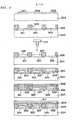
- Fig. 1shows a first embodiment of the manufacturing method of the organic EL element according to the present invention.
- This figureshows the manufacturing method of a full color organic EL element with three colors.
- this inventionis directed to a method of manufacturing an organic EL element which comprises a step of forming pixel electrodes 101, 102 and 103 on a transparent substrate (transparent support) 104, a step of patterning luminescent layers 106 and 107 which are made of organic compounds on the respective pixel electrodes, and a step of forming a cathode 113, wherein the method is characterized in that the formation of the luminescent layers is carried out by means of an ink-jet method.
- the transparent substrate 104functions not only as a support but also as a surface through which light is taken out. Accordingly, the material for the transparent substrate 104 is selected by taking the light-permeability, thermal stability and the like into consideration. As for examples of the material to be used for the transparent substrate, glass, transparent plastic or the like can be mentioned, and among these materials, a substrate made of glass is particularly preferable in view of its excellent heat resistance.
- the first, pixel electrodes 101, 102 and 103are formed on the transparent substrate 104.
- photolithography, vacuum deposition method, sputtering method and pyrosol methodcan be mentioned.
- the photolithographyis particularly preferable.
- these pixel electrodesit is preferred that they are formed into transparent pixel electrodes.
- the materials constituting the transparent pixel electrodesa tin oxide film, an ITO (indium tin oxide) film and a composite oxide film of indium oxide and zinc oxide can be mentioned.
- partitioning walls (banks) 105are formed to fill the spaces between the pixel electrodes.
- the materials constituting the banks 105no particular limitation is imposed, if they have a resistance to the solvent for the EL material.
- organic materialsuch as acrylic resin, epoxy resin, photosensitive polyimide and the like; and inorganic material such as liquid glass and the like can be mentioned.
- the banks 105may be formed into a black resist which is formed by mixing carbon black and the like into the above-mentioned material.
- organic luminescent layersare formed respectively on the pixel electrodes according to a predetermined pattern.
- a red luminescent layer 106 and a green luminescent layer 107are formed on the pixel electrodes 101 and 102, respectively, by the ink-jet method.
- the term "ink-jet method”is used to mean a method of forming a pixel of one of the three primary colors including red, green and blue or a pixel of at least one color which is intermediate between the primary colors by dissolving or dispersing a luminescent material in a solvent to obtain a discharge liquid and then discharging the discharge liquid from a head 110 of an ink-jet device 109.
- an ink-jet methodit is possible to carry out fine patterning in a simple manner and in a short time. Further, it is also possible to control easily and freely the luminescent characteristics such as color balance and brightness (luminance) by adjusting the thickness of the layer through adjustment of the discharge amount of the ink or by adjusting the ink concentration.
- the luminescent layersare formed by discharging the luminescent materials by the ink-jet method to carry out patterning, and then conjugating (to form a film) the precursor components by heating or irradiation with light or the like.
- a blue luminescent layer 108is formed on the red luminescent layer 106, the green luminescent layer 107 and the pixel electrode 103.
- the forming method for the blue luminescent layer 108No particular limitation is imposed upon the forming method for the blue luminescent layer 108, and it is possible to form the layer using the general film forming method known as deposition method or wet method, for instance, or using the ink-jet method.
- the blue luminescent layer 108can be formed of an electron injection and transfer material such as aluminum quinolynol complex. In this case, it is possible to promote the injection and transfer of the carriers so as to improve the luminous efficiency. Furthermore, when such a blue luminescent layer 108 is laminated with red and green luminescent layers formed of a hole injection and transfer material described later, it is also possible to inject and transfer the electrons and the holes from the respective electrodes into these laminated luminescent layers with appropriate balance, thereby enabling to improve the luminous efficiency.
- an electron injection and transfer materialsuch as aluminum quinolynol complex.
- the function of hole injection and transfer and the function of electron injection and transfercan be assigned separately to different layers, so that optimum design can be selected for the respective materials.
- No particular limitationis imposed upon the forming method of such an electron injection and transfer layer, and it is possible to form the layer by using, for example, the general film forming method known as deposition method or wet method or the ink-jet method.
- an organic compound which can form an electron injection and transfer layeroxadiazole derivative such as PBD, OXD-8 and the like, DSA, aluminum quinolinol complex, Bebq, triazole derivative, azomethine complex, porphine complex, benzoxadiazol and the like can be mentioned.
- an electron injection and transfer layercan be formed from just one of these materials, or formed by mixing or laminating one of or two or more of them.
- the electron injection and transfer layermay be formed by doping a fluorescence dye described later to the organic compound described. Further, the electron injection and transfer layer itself may have a function of luminescence.
- organic luminescent layers for two colorsare formed by the ink-jet method while the layer for the remaining one color is formed by a different method. Therefore, according to this embodiment, even when a luminescent material which is not so suited for the ink-jet method is used, a full color organic EL element can be formed by using such a material in a combination with other organic luminescent materials that are suited for the ink-jet method, so that the latitude in the design for the EL element will be expanded.
- the forming method for the luminescent layer other than the ink-jet methodphotolithography method, vacuum deposition method, printing method, transfer method, dipping method, spin coating method, casting method, capillary method, roll coating method, bar coating method and the like can be mentioned.
- a cathode (a counter electrode) 113is formed, thereby the organic EL element of the present invention is completed.
- the cathode 113is formed into a metallic thin film electrode, and as for examples of the metal for forming the cathode, Mg, Ag, Al, Li and the like can be mentioned.
- a material having small work functioncan be used for the material for the cathode 113, and for example, alkali metal, alkali earth metal such as Ca and the like, and alloys containing these metals can be used.
- Such a cathode 113may be formed using a deposition method, a sputtering method or the like.
- the organic EL element of the present inventionis manufactured through the processes described in the above. Namely, as shown in Fig. 1, the pixel electrodes 101 and 102 are provided on the transparent substrate 104, the red luminescent layer106 and the green luminescent layer 107 which are made of organic compounds are then formed on the pixel electrodes 101 and 102, respectively, by patterning by using the ink-jet method, and then the blue luminescent layer 108 is formed on the luminescent layers 106 and 107 and the pixel electrode 103 by the vacuum deposition method. Thereafter, the cathode 113 is formed on top of the blue luminescent layer 108, thereby the organic EL element according to the present invention is completed.
- a protective film 415may be formed on top of a cathode 413.
- a protective film 415it becomes possible to prevent deterioration, damage, peeling and the like from occurring in the cathode 413 and in the luminescent layers 406, 407 and 408.
- the protective film 415As for materials for constructing the protective film 415, epoxy resin, acrylic resin, liquid glass and the like can be mentioned. Further, as for examples of the forming method for the protective film 415, spin coating method, casting method, dipping method, bar coating method, roll coating method, capillary method and the like can be mentioned.
- these luminescent layersare formed of an organic compound, and it is more preferable that these luminescent layers are formed of a polymer organic compound.
- organic compoundBy providing such luminescent layers that are formed of the organic compound, it is possible to obtain high brightness surface luminescence at low voltages. Further, since luminescent materials can be selected from wide range of field, a rational design for the luminescent element becomes possible.
- polymer organic compoundshave an excellent film formation property, and the luminescent layers composed of polymer organic compounds have an extremely good durability. Further, these polymer organic compounds have a band gap in the visible region and a relatively high electrical conductivity. Among such polymer organic compounds, a conjugated polymer can exhibit such properties prominently.
- materials for the organic luminescent layerspolymer organic compound itself, precursor of conjugated organic polymer compound which is to be conjugated (to form a film) by heating or the like, and other materials are used.
- the viscosity or the like of a discharge liquid used for the ink-jet systemcan be adjusted easily, so that the patterning is carried out precisely and the luminescence characteristics and the film properties of the luminescent layer can be controlled easily.
- the polymer organic compound forming the luminescent layersis a hole injection and transfer material. In this way, it is possible to promote the injection and transfer of the carriers and thereby to improve the luminous efficiency.
- polyalkylthiophenesuch as PPV (poly(para-phenylene vinylene)) or its derivative, PTV (poly(2,5-thienylene vinylene)) and the like; polyallylene vinylene such as PFV (poly(2,5-furylene vinylene)) polyparaphenylene, polyalkylfluorene and the like; pyrazoline dimer; quinolizine carboxylic acid; benzopyrylium perchlorate; benzopyranoquinolizine; rubrene; phenanthroline europium complex and the like can be mentioned. In this case, just one of them or a mixture of two or more of them can be selectively used.
- PPVwhich is a conjugated organic polymer compound or its derivative is preferable.
- the precursor prior to conjugation (to form a film) of PPV or its derivativeis soluble to water or organic solvent, so that they are suitable for pattern formation by the ink-jet method. Further, it is possible to obtain a thin layer which has high optical quality and excellent durability, since it is a polymer.
- PPV or its derivativepossesses a strong fluorescence, and since it is a conductive polymer in which ⁇ -electron of double bond is delocalized on the polymer chain, a thin film of PPV also functions as a hole injection and transfer layer, which makes it possible to obtain an organic EL element having high performance.
- the composition for an organic EL element in a case where a polymer organic compound is used for the material for the luminescent layersmay include at least one kind of fluorescent dye in it.
- fluorescent dyeBy including such fluorescent dye way, it becomes possible to change the luminous property of the luminescent layer. Therefore, the addition of the fluorescent dye is effective as a means, for example, for improving the luminous efficiency of the luminescent layer or for changing the maximum wavelength of light absorption (emitted color) of the luminescent layers.
- a fluorescent dyecan be utilized not only as a material for the luminescent layers but also as a material for the coloring matter which has the luminescence function itself.
- almost all of the energy of the excitons which are generated by the recombination of carriers on the molecules of a conjugated organic polymer compound such as PPVcan be transferred onto the molecules of the fluorescent dye.
- the current quantum efficiency of the EL elementis also increased, because the luminescence arises only from the molecules of the fluorescent dye which have a high fluorescence quantum efficiency.
- the addition of a fluorescent dye into the composition for the organic EL elementthe luminescence spectrum of the luminescent layer becomes at the same time the spectrum of the fluorescent dye, whereby this method becomes also an effective means for changing the emitted color.
- the changes in the maximum wavelength of light absorption induced by the doping of a fluorescent dyemake it possible, for example, to emit the three primary colors of red, green and blue, thereby enabling to obtain a full color display device.
- the doping of the fluorescent dyemakes it possible to improve extremely the luminous efficiency of the EL element.
- a fluorescent dye used for the red luminescent layerlaser dye DCM, rhodamine or a rhodamine derivative, perylene and the like can be used. These fluorescent dyes are soluble to solvents because they are low molecules, and have a high compatibility with PPV or the like, so that a luminescent layer with a good uniformity and good stability can be formed easily.
- the rhodamine derivative fluorescent dyesrhodamine B, rhodamine B base, rhodamine 6G, rhodamine 101 perchlorate can be mentioned. In this case, a mixture of two or more of them can be selectively used.
- fluorescent dye used in the green luminescent layerquinacridone, rubrene, DCJT and their derivatives can be mentioned. Since these fluorescent dyes are low molecules in the same manner as the fluorescent dyes to be used in the above-mentioned red luminescent layer, they are soluble to solvents and have a high compatibility with PPV or the like, so that the luminescent layer can be formed easily.
- fluorescent dye used in the blue luminescent layerdistyrylbiphenyl and its derivative can be mentioned. These fluorescent dyes are soluble to aqueous solutions in the same manner as the above-mentioned fluorescent dyes for the red luminescent layer, and have high compatibility with PPV or the like, so that the luminescent layer can be formed easily.
- coumarinAs for other fluorescent dyes that can be used in the blue luminescent layer, coumarin; and coumarin derivatives such as coumarin-1, coumarin-6, coumarin-7, coumarin 120, coumarin 138, coumarin 152, coumarin 153, coumarin 311, coumarin 314, coumarin 334, coumarin 337, coumarin 343 and the like can be mentioned.
- tetraphenylbutadiene (TPB) or TPB derivative, DPVBi and the likecan be mentioned. Since these luminescent materials are also low molecules in the same manner as the fluorescent dyes for the red luminescent layer, they are soluble to solvents, and have high compatibility with PPV or the like, so that the luminescent layer can be formed easily.
- fluorescent dyes and luminescent materials as described abovecan be selectively used as a just one of them or as a mixture of two or more of them.
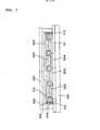
- a head of the ink-jet system used in the manufacturing method of the organic EL element according to the present inventionis shown in Fig, 10 and Fig. 11.
- the head 10 for the ink-jet systemis provided with, for example, a stainless steel nozzle plate 11 and a vibration plate 13, and they are coupled via partitioning members (reservoir plates) 15.
- a liquid storage 21 and a plurality of spaces 19are formed by means of the reservoir plates 15.
- the inside of the respective spaces 19 and the liquid storage 21are filled with the composition according to the present invention, and the spaces 19 communicate with the liquid storage 21 through supply ports 23.
- a nozzle hole 25is provided in the nozzle plate 11 for discharging the composition in a jet-form from the spaces 19.
- a hole 27is formed in the vibration plate 13 for supplying the composition to the liquid storage 21.
- piezoelectric elements 29are attached at positions corresponding to the positions of the respective spaces 19.
- Each of the piezoelectric elements 29is positioned between a pair of electrodes 31.
- the piezoelectric element 29is adapted to bend so as to protrude outward when energized, and at the same time, the vibration plate 13 to which the piezoelectric element 29 is attached is also bent outward together with the piezoelectric element 29. In this way, the volume of the space 19 is increased. With this result, a quantity of the composition corresponding to the increased volume flows into the space 19 from the liquid storage 21 through the supply port 23.
- both the piezoelectric element 29 and the vibration plate 13return to their original shapes.
- the space 19also returns to its original volume, so that the pressure exerted to the composition within the space 19 goes up, whereby the composition is jetted out from the nozzle hole 25 toward the substrate.
- a water repellent layer 26is formed at the peripheral part of the nozzle hole 25 in order to prevent the bend of the jetted direction of the composition and the clogging of the hole from occurring.
- a water repellent layer 26 formed of, for example, a Ni-tetrafluoroethylene eutectoid plated layeris provided in the peripheral part of the nozzle hole 25 as shown in Fig. 11.
- compositions with the following characteristicscan be used as organic luminescent materials for the ink-jet method.
- the compositionshave a contact angle of 30 to 170 degrees, and more preferably, 35 to 65 degrees, with respect to the material constituting the nozzle surface 251 of the nozzle provided in the head for the ink-jet system for discharging the composition.
- the compositionhas the contact angle given in this range, it is possible to carry out a precise patterning by suppressing the bend in the jetted direction of the composition.
- the contact angleis less than 30 degrees, wettability of the composition with respect to the material constituting the nozzle surface increases, so that there is a case that the composition attaches asymmetrically to the periphery of the nozzle hole at the time of discharging the composition.
- an attractionacts between the composition attached to the nozzle hole and the composition to be discharged. This causes the discharge of the composition by a non-uniform force, which gives rise to a situation so-called "bend in the jetted direction" in which the composition is unable to reach the target position, and also to an increase in the occurrence frequency of the bend in the jetted direction.
- the bend in the jetted directionrefers to a situation in which, when the composition is discharged from the nozzle, the point of impact of a dot deviates from the target position by more than 50 ⁇ m.
- the occurrence frequency of the bend in the jetted directionis defined as the time until the bend in the jetted direction occurs after a continuous discharge of the composition is started at the frequency of 7200Hz.
- the bend in the jetted directionis generated principally by such causes as the nonuniformity in the wettability of the nozzle hole and the clogging of the nozzle hole by the attachment of solid components of the composition. Such bend in the jetted direction can be eliminated by cleaning the head.
- an occurrence frequency of the bend in the jetted directionis required to be more than 1000 seconds.
- the viscosity of the compositionis 1 to 20cp, and more preferably 2 to 4cp. If the viscosity of the composition is less than 1cp, the contents of the precursor and the fluorescent dye in the material are too small, so that the luminescent layer which is formed cannot exhibit luminescence power sufficiently. On the other hand, if it exceeds 20cp, it is impossible to discharge the composition smoothly from the nozzle, and it becomes difficult to carry out patterning unless otherwise such a change in the specification as the enlargement of the diameter of the nozzle hole is introduced. In addition, when the viscosity of the composition is high, precipitation of the solid components in the composition tends to occur, thus leading to an increased occurrence frequency of clogging of the nozzle hole.
- the compositionhas the surface tension of 20 to 70 dyne/cm, and more preferably 25 to 40 dyne/cm.
- the surface tensionis less than 20 dyne/cm, the wettability of the composition with respect to the material constituting the nozzle surface increases, which results in the occurrence of the bend in the jetted direction, and an increase in the occurrence frequency of the bend in the jetted direction, similar to the case of the contact angle.
- it exceeds 70 dyne/cmthe shape of the meniscus at the tip of the nozzle is not stable, which results in the difficulty in the control of the amount and the timings of discharge of the composition.
- composition of the organic luminescent material suitable for the manufacturing method of the organic EL element of this inventionit needs to satisfy the condition on the numerical range for at least one of the characteristics including the contact angle, the viscosity and the surface tension described above.
- a composition which satisfies the conditions for the arbitrary combination of two characteristicsis more preferable, and a composition which satisfies the conditions for all the characteristics is most preferable.
- Fig. 2shows a second embodiment of the manufacturing method of the organic EL element according to the present invention.
- a red luminescent layer 206 and a green luminescent layer 207are formed by using an ink-jet method in the same manner as the first embodiment.
- This second embodimentis different from the first embodiment in the point that a hole injection and transfer layer 208 is formed on the pixel electrode 203 and then a blue luminescent layer 210 is laminated on the layer 208.
- a hole injection and transfer layer 208is formed on the pixel electrode 203 and then a blue luminescent layer 210 is laminated on the layer 208.
- the manufacturing method for the organic EL element according to the present inventionit is preferable to laminate a hole injection and transfer layer with at least one luminescent layer with a certain color. In this way, it is possible to improve the luminous efficiency and to improve the stability of the thin film element itself.
- the hole injection and transfer layer 208is a non-luminescent layer. With this arrangement, it is possible to make a region of the blue luminescent layer 210 positioned above the pixel electrode 203 to be a luminescent portion, thereby enabling to fabricate a full color organic EL element more easily.
- aromatic diamine based compoundsuch as TPD; MTDATA; quinacridone; bisstil anthracene derivative
- PVKpolyvinyl carbazole
- phthalocyanine based complexsuch as copper phthalocyanine
- porphin based compoundNPD; TAD; polyaniline; and the like
- PVKis particuraly preferred.
- the organic EL element according to the present inventioncan be obtained by forming a blue luminescent layer 210 and a cathode 211 in the same way as the first embodiment.
- the materials constituting the blue luminescent layer 210 and the cathode 211 and the manufacturing method thereofare the same as those of the first embodiment.
- Fig. 3shows a third embodiment of the manufacturing method for the organic EL element according to the present invention.
- a red luminescent layer 306 and a green luminescent layer 307are formed in the same manner as the first embodiment.
- a hole injection and transfer layer 308is formed on the entire surface of the red luminescent layer 306, the green luminescent layer 307 and the pixel electrode 303.
- the hole injection and transfer layer 308is formed into a non-luminescent layer.
- hole injection and transfer layer 308No particular limitation is imposed upon the forming method for the hole injection and transfer layer 308, and for example, ink-jet method, vacuum deposition method, dipping method, spin coating method, casting method, capillary method, roll coating method, bar coating method and the like can be mentioned.
- the hole injection and transfer layercan be formed using the vacuum deposition method.
- the material constituting the hole injection and transfer layer 308the same materials as those mentioned in the second embodiment can be used.
- the organic EL element according to the present inventioncan be obtained.
- the constituent material and the forming method of the cathode 311are the same as those of the above-mentioned embodiments.
- Fig. 4shows a fourth embodiment of the manufacturing method for the organic EL element according to the present invention.
- luminescent layers 806, 807 and 808are patterned on the pixel electrodes 801, 802 and 803, respectively, by the ink-jet method.
- the amount of the material to be discharged for the respective luminescent layers, the number of times of the discharge and the formation pattern of the luminescent layers, for example;can be adjusted easily and handily, so that the luminescent characteristics and film thickness and the like of the respective luminescent layers can be controlled easily.
- an electron injection and transfer layer 811is formed on the luminescent layers 806, 807 and 808.
- the electron injection and transfer layer 811facilitates the injection of the electrons from the cathode, and contributes to the prevention of electrode extinction by keeping the luminescent portions away from the cathode to establish a better contact with the cathode.
- the electron injection and transfer layer 811aluminum quinolynol complex to which the doping is not carried out can be used.
- This electron injection and transfer layer 811can be formed by means of a vacuum deposition method.
- the forming method for the electron injection and transfer layer 811is not limited to this method, and for example, the ink-jet method, vacuum deposition method, dipping method, spin coating method, casting method, capillary method, roll coating method, bar coating method or the like can be used.
- the organic EL element according to the present inventioncan be obtained by forming a cathode 813 on top of it.
- the constituent material and the formation method of the cathode 813are the same as those of the above-mentioned embodiments.
- Fig. 5shows a fifth embodiment of the manufacturing method of the organic EL element according to the present invention.
- pixel electrodes 801, 802 and 803are first formed on a transparent substrate 804 in the same manner as the first embodiment. Then, a hole injection and transfer layer 815 which is for example made of PVK is formed on the entire surfaces of the pixel electrodes by means of, for example, a spin coating method. Accordingly, since the hole injection and transfer layer 815 in this embodiment can be formed by means of coating without need of patterning, it is possible to increase manufacturing efficiency.
- hole injection and transfer layer 815No particular limitation is imposed upon the forming method for the hole injection and transfer layer 815, and for example, ink-jet method, vacuum deposition method, dipping method, spin coating method, casting method, capillary method, roll coating method, bar coating method and the like can be used.
- the hold injection and transfer layer 815is formed into a non-luminescent layer.
- luminescent layers 806, 807 and 808are formed on top of the hole injection and transfer layer 815.
- at least one luminescent layer for a certain coloris formed by pattering using the ink-jet method carried by the ink-jet device 809.
- an organic EL element according to the present inventioncan be obtained.
- the structural material for the cathode 813 and the manufacturing method thereofare the same as those of the other embodiment described above.
- the organic EL element of the present inventioncan be manufactured according to the manufacturing methods described above with reference to the embodiments.
- the present inventionis not limited to the structures provided by these methods, and the following structures can be adopted, for instance.
- Fig. 15is a partial cross-sectional view which shows other embodiment of an organic EL element according to the present invention.
- the organic EL element of this embodimenthas a construction in which a reflection layer 62, a transparent conductive film (ITO film) 63, a hole injection and transfer layer 64, an organic luminescent layer 65, a metal layer 66 and a transparent conductive layer (ITO film) 67 are laminated on a transparent substrate 61 in this order.
- a reflection layer 62a transparent conductive film (ITO film) 63
- a hole injection and transfer layer 64an organic luminescent layer 65
- a metal layer 66 and a transparent conductive layer (ITO film) 67are laminated on a transparent substrate 61 in this order.
- the reflection layer 62which is made from a metal thin film such as Al is provided directly.
- the metal layer 66 which is laminated onto the luminescent layer 65 as a cathodeis extremely thin (approximate to 10 to 50 ⁇ ), so that the metal layer has a light permeability so as to pass emitted light from the luminescent layer 65 therethrough.
- the metal layersince the metal layer is extremely thin, its value of resistance is high and therefore its conductivity is insufficient. Therefore, the metal layer can not sufficiently exhibit function as the cathode.
- the transparent conductive film (ITO film) 67is laminated onto the metal layer 66.
- such a metal layer 66can be made from Al - Li alloy or the like for example, and it can be formed using the vacuum deposition method, sputtering method or the like.
- Fig. 7is an illustration which shows an embodiment of an organic EL display device according to the present invention.
- a bus line (gate line) 511 made of Alis formed on a glass plate 501 by means of a photolithography patterning method, and a thin film transistor (not shown in the drawing) is formed thereon to constitute the ITO transparent pixel electrode 504 and the like.
- a red luminescent layer 502 and a green luminescent layer 503are formed by means of the ink-jet method, and then a blue luminescent layer 505 is formed by means of the vacuum deposition method.
- a cathode 506is formed by means of the vacuum deposition method, thereby constructing the organic EL element same as the first embodiment described above.
- a protective base material 507is stuck onto the transparent substrate 501 in a fixed manner by means of a peripheral seal 509.
- this assemblyis placed in an inert gas atmosphere such as argon gas or the like, and thereby introducing the inert gas inside thereof from a seal opening 513 and then the seal opening 513 is sealed with a seal member 508.
- an inert gas atmospheresuch as argon gas or the like
- the seal member 508is formed form a material through which the inert gas 512 does not penetrate.
- a silver paste 510has a function that realizes a contact between the cathode 506 and the gate line 511 on the element.
- Gate lines 511are provided to control ON and OFF of the thin film transistors (TFT), which are provided in the respective display pixels, in each line of the pixels in order to select pixels to be displayed.
- TFTthin film transistors
- potential of the gate line for one line of pixelsis turned into a selected level, thereby bringing the TFTs on this line into a conductive state.
- the voltages of the picture signalsare applied to the pixel electrodes through the TFTs, thereby enabling to charge the potentials to the pixels to a level of a signal voltage and then discharge them.
- Fig. 8is an illustration which shows other embodiment of an active matrix type organic EL display device using the organic EL element according to the present invention.
- This organic EL display device of this embodimentincludes an pixel arrangement comprised of a plurality of luminescent pixels which are arranged in a matrix form and which are formed into any one of R, G and B luminescent elements.
- signal lines (signal electrodes) 601 and gate lines (gate electrodes) 602which are arranged in a matrix form so as to be orthogonal to each other.
- a thin film transistor (TFT) 604which is connected to both the signal line 601 and the gate line 602 is provided, and a luminescent layer 605, 606 which is formed of the organic EL element and connected to the TFT is laminated on the TFT.
- TFTthin film transistor
- luminescent layer 605, 606which is formed of the organic EL element and connected to the TFT is laminated on the TFT.
- at least one luminescent layer for any one of colors R, G, Bis formed by means of the ink-jet method.
- Fig. 9is a sectional view which shows one example of the manufacturing method of the active matrix type organic EL display device according to the present invention.
- a transparent substrate 904predetermined thin film transistors 915 as well as gate lines and signal lines (not shown) and the like are formed.
- hole injection and transfer layers 911are formed so as to cover the respective pixel electrodes.
- the hole injection and transfer type materialthe same materials that are discussed in this specification with reference to the previous embodiments can be used.
- the method of forming the hole injection and transfer layer 911is not limited to a specific method, and it is possible to form the layer by means of any method described above.
- respective luminescent layers 906red), 907 (green) and 908 (blue) are formed by patterning.
- at least one layer for one coloris formed by the ink-jet method using an ink-jet device 910.
- a reflection electrode 913is formed, thereby completing the organic EL display device according to the present invention.
- Mg - Ag electrodehaving a thickness of about 0.1 to 0.2 ⁇ m or the like is formed, for instance.
- a thin film transistoris used as a switching element, but the present invention is not limited thereto.
- Other switching elements and two-terminal elementsuch as MIM can be used.
- the display devicemay be configured into a passive drive type or a static drive type (static image, segment display).
- the number of the switching elementis not limited to one per one pixel.
- a plurality of switching elementsmay be provided per one pixel.
- Fig. 12shows an embodiment of an organic EL display device in which a plurality of switching elements are provided per one pixel.
- a switching type thin film transistor 142carries out a role that transmits the potential at a signal electrode 132 to a current thin film transistor 143 in response to the potential at a scanning electrode 131, and the current thin film transistor 143 carries out a role that controls electrical connection between the common electrode 133 and the pixel electrode 141.
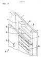
- Fig. 13is a perspective view which roughly shows a structure of the organic EL display device according to the present invention.
- a scanning electrode 53 and a signal electrode 54which are formed into an elongated strip, respectively, are arranged outside the organic EL element 52 so that scanning lines extending from the scanning electrode 53 and the signal lines extending from the signal electrode 54 are orthogonal to each other through the organic EL element.
- Such a passive matrix type display deviceis driven by selecting scanning lines of the scanning electrode 53 in a pulsed manner in a sequential order while a voltage is applied to signal lines of the signal electrode 54 corresponding to pixels to be displayed on the scanning line. Such selection of the lines is carried out by a controller 55.
- a cathodeis patterned so as to be separate forms to correspond to each of lines.
- a cathode having a thickness of about 0.2 ⁇ mis formed according to the third embodiment, such separate forms of the cathode can be automatically obtained since the cathode is separated by the banks.
- Such a cathodeis formed by the patter formation performed by a masking deposition method or a laser cutting method, for instance.
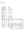
- Fig. 14is a diagram which shows one example of wave forms of driving voltages applied to the scanning electrode 13 and signal electrode 14, respectively.
- the wave forms shown in the drawingare determined so as to be able to apply a voltage Vs which is sufficient to luminescence to selected pixels.
- the brightness of a pixel to be displayedis controlled through the width of the pulse from the signal electrode 14 that has been determined so as to meet with a gray scale of the brightness to be displayed.
- a voltage Vnwhich is lower than a luminescent threshold voltage is applied to respective non-selected pixels.
- Tfshows a scanning timing.
- the scanning signalis driven by a pulse having a duty ration of 1/100.
- the luminescence of the blue luminescent layer 808 of the organic EL display device comprised of the organic EL elements of the fourth embodimentwas a brightness of 100 cd/m2 at a driving voltage of 20V.
- ITO transparent pixel electrodes 101, 102 and 103were formed by means of photolithography so as to form a pattern having a pitch of 100 ⁇ m and a thickness of 0.1 ⁇ m.
- the spaces between the ITO transparent pixel electrodeswere buried, and then banks 105 which act not only as a light cut-off layer but also an ink drop preventing wall were formed by photolithography.
- the banks 105were designed so as to have a width of 20 ⁇ m and a thickness of 2.0 ⁇ m.
- a Mg - Ag electrode 113 having a thickness of 0.8 ⁇ mwas formed as a cathode using a vacuum deposition method to obtain an organic EL element.
- ITO transparent pixel electrodes 201, 202, 203were formed on a glass substrate 204 as shown in Fig. 2. Thereafter, the spaces between the ITO transparent pixel electrodes were buried and then resists (partitioning walls) 205 made of a light-sensitive polyimide and functioning not only as a light cut off layer but also an ink drop preventing wall were formed.
- a hole injection and transfer layer made of polyvinyl carbazole (PVK)was patterned on the transparent pixel electrode 203 by means of the ink-jet device 209. Then, a blue luminescent layer 210 was formed by coating the pyrazoline dimer on top of the hole injection and transfer layer.
- PVKpolyvinyl carbazole
- an Al - Li electrode 211 having the thickness of 0.8 ⁇ mwas formed as the cathode by the deposition method, and thereby the organic EL element was manufactured.
- ITO transparent pixel electrodes 801, 802 and 803 and banks 805were formed on a glass substrate 804 as shown in Fig. 4 in the same way as Example 1.
- an organic hole injection and transfer type materialwas mixed in the luminescent materials shown in Table 1 and Table 2 to form luminescent layers 806 (red), 807 (green) and 808 (blue) by using an ink-jet device 809.
- the vacuum depositionwas carried out using the aluminum quinolynol complex to which the doping was not carried out to form an electron injection and transfer layer 811 having the thickness of 0.1 ⁇ m.
- an Al - Li electrode 813 having the thickness of 0.2 ⁇ mwas formed as the cathode by the deposition method, and thereby the organic EL element was manufactured.
- ITO transparent pixel electrodes 301, 302 and 303 and banks 305were formed on a glass substrate 304 as shown in Fig. 3.
- a hole injection and transfer layer 308 made of polyvinyl carbazole (PVK)was formed on the entire surfaces of the luminescent layers 306, 307 and the transparent electrode 303 by means of the coating method.
- a blue luminescent layer 309 made of a distyryl derivativewas formed on the hole injection and transfer layer 308 by means of the vacuum deposition method.
- an Al - Li electrode 311 having the thickness of 0.8 ⁇ mwas formed as the cathode by the deposition method, and thereby the organic EL element was manufactured.
- the cathode 311was automatically separated and then insulated by the formation of the banks 304, the cathode was brought into a condition that is was patterned so as to correspond to the respective pixels 301, 302 and 303.
- ITO transparent electrodes 801, 802 and 803 and banks 805were formed on a glass substrate 804 as shown in Fig. 4.
- the vacuum depositionwas carried with the aluminum quinolynol complex to which the doping was not carried out to form the electron transfer layer 811 having the thickness of 0.1 ⁇ m.
- an Al - Li electrode 812 having the thickness of 0.8 ⁇ mwas formed as the cathode by the vacuum deposition, so that the organic EL element was manufactured.
- a prescribed voltagewas applied to the element, and the applied voltage at which a luminance of 1 cd/m 2 is observed was defined as the luminescence starting voltage [Vth].
- the initial luminance after applying a stabilization treatmentwas set to 100%. and the changes in the luminance of the EL element were measured when subjecting it to continuous luminescence through supply of a constant current of standard waveform, wherein the luminescence life is defined as the time until the luminance drops to 50% of the initial luminance.
- the drive conditions for this experimentwere set at 40°C for room temperature, 23% for humidity and 20 mA/cm 2 for current density.
- the luminancewas measured, in which the current was set to 20 mA/cm2.
- the wavelength at maximum absorption for each luminescent layerwas measured.
- the luminescent layers in Examples 1 to 5have excellent luminescence characteristics and excellent film characteristics.
- the luminescent layerswere formed of polymer organic compounds, no defects were observed in the luminescent layers, and extremely favorable thin films were obtained.
- compositions for the organic EL elements and the manufacturing methods for the organic EL elements according to the present inventionhave been described according to the embodiments that are illustrated.
- the present inventionis not limited to these embodiments, and for example, there may be inserted in the manufacturing processes for providing any intermediate functional layers between the respective layers.
- the fluorescent dyes which are added for changing the luminescence characteristicsare not limited to those described above.
- a layer made of, for example, 1,2,4-triazole derivative (TAZ)may be provided as a buffer layer between the respective layers, thereby enabling to more improve the luminance, luminescence life and the like.
- TEZ1,2,4-triazole derivative
- the manufacturing method for the organic EL elements according to the present inventionmay include a further process in which surface treatment such as plasma, UV treatment, coupling or the like are applied to the surface of the resin resists, the pixel electrodes and the underlying layers in order to facilitate the sticking of the EL materials.
- surface treatmentsuch as plasma, UV treatment, coupling or the like
- the organic EL display devicemay be applied to the low information field, such as segment display and still image display of whole surface simultaneous luminescence, for example, display of pictures, characters, labels, or may be utilized as a light source having point, line, or surface shape.
- the manufacturing method of the organic EL element of the present inventionit is possible to explore rational design of the EL luminescent elements through a wide ranging selection of the luminescent materials. For example, through arbitrary combinations of the luminescent materials and fluorescent dyes, it is possible to obtain wide variety of display lights.
- the organic luminescent materialsit is possible to obtain the diversified designs of the EL element having high luminance and long life.
- the ink-jet-methodFurthermore, by carrying out the pattern forming and arrangement of the luminescent layer for at least one color, the hole injection and transfer layer and the electron injection and transfer layer by means of the ink-jet-method, it is possible to set arbitrarily and precisely the size and the pattern of the luminescent elements.
- a precursorwhich can be conjugated (form a film) by thermosetting
- thermosettingWhen a precursor, which can be conjugated (form a film) by thermosetting is used as a luminescent material, the latitude in the setting of conditions such as viscosity can be expanded, and the adjustment of the conditions suitable as a discharge liquid for the ink-jet method can be facilitated.
- conditions such as the film thickness, the number of dots and the likecan be adjusted arbitrarily, so that it is possible to control readily the luminescence characteristics of the luminescent layers.
- the ink-jet methodit is possible to move freely the head on the transparent substrate, thereby enabling to form an element with an arbitrary size without restricting the dimensions of the substrate. Moreover, since required amounts of materials can be arranged at required locations, it is possible to maximally exclude the uselessness of waste liquid or the like. In this way, manufacturing of a full color display device with large screen size becomes possible at a low cost.
Landscapes
- Engineering & Computer Science (AREA)
- Manufacturing & Machinery (AREA)
- Physics & Mathematics (AREA)
- Optics & Photonics (AREA)
- Electroluminescent Light Sources (AREA)
- Luminescent Compositions (AREA)
- Devices For Indicating Variable Information By Combining Individual Elements (AREA)
Abstract
Description
The present invention relates to a method of manufacturing anorganic electroluminescent (EL) element, an organic EL element, andan organic EL display device.
An organic EL element is an element which has a configurationin which a thin film containing a fluorescent organic compound is heldbetween a cathode and an anode. In the organic EL element, electronsand holes are injected from the respective electrodes into the thinfilm to generate excitons through the recombimation of the electronsand holes. The organic EL element produces luminescence by utilizingemission of light (fluorescence or phosphorescence) at thedeactivation of the excitons.
The features of the organic EL element is that it is possibleto obtain a high intensity surface luminescence on the order of 100to 100,000 cd/m2 at a low voltage of less than 10V, and that it ispossible to produce luminescence of from blue to red by the selectionof the kind of fluorescent material.
The organic EL element is drawing attraction as a device forrealizing a large area full color display element at a low cost (see,Technical Reports of the Society of Electronic Information andCommunications, Vol. 89, No. 106, 1989, p. 49). According to thereport, bright luminescence of blue, green and red were obtained byforming a luminescent layer using an organic luminescent materialwhich emits strong fluorescence. This fact is considered to mean thatit is possible to realize a high brightness full color display by usingan organic coloring matter which emits strong fluorescence in a thinfilm state and has less pin hole defects.
In addition, in Japanese Laid-Open Publication No. Hei 5-78655,there is proposed to use an organic luminescent layer containing aluminescent material which is formed of a mixture of an organiccharging material and an organic luminescent material, therebyobtaining a high brightness full color element by preventing quenchingdue to higher concentration as well as expanding the latitude in theselection of the luminescent material.
Further, in Appl. Phys. Lett. Vol. 64, 1994, p. 815, it isreported that a white luminescence was obtained by using polyvinylcarbazole (PVK) as a luminescent material and doping it with coloringmatters corresponding to three primary colors R, G and B. However,in neither of the above references, the configuration or the methodof manufacture of an actual full color display panel is not shown.
In the organic thin film EL elements using the organicluminescent materials described above, in order to realize a full colordisplay device, it is necessary to arrange organic luminescent layerswhich emit any one of the three primary colors for the respective pixels.However, there is a problem in that a polymer or precursor that formsthe organic luminescent layer lacks a sufficient resistance to apatterning process such as photolithography, so that it is verydifficult to carry out patterning with highly precision.
Further, when several organic layers are to be formed by a vacuumdeposition method, it takes a long time. Therefore, such a methodcannot be said to be an efficient method of manufacturing the element.
It is an object of the present invention to provide a methodof manufacturing an organic EL element which makes it possible to carryout patterning easily and precisely, can attain optimization of a filmdesign in a simple manner, and has excellent luminescencecharacteristics, as well as to provide an organic EL element and anorganic EL display device.
In order to achieve the above object, the manufacturing methodof an organic EL element according to the present invention comprisesthe steps of forming pixel electrodes on a transparent substrate,forming on the pixel electrodes by patterning at least one luminescentlayer having a certain color and made of an organic compound, andforming a counter electrode opposing the pixel electrodes, whereinthe formation of the luminescent layers is performed by means of anink-jet method.
In the present invention, it is preferable that the organiccompound is a polymer organic compound. In this case, it is preferablethat the polymer organic compound is a hole injection and transfertype material. Preferably, such a polymer organic compound is apolyparaphenylene vinylene or its derivative or a copolymer whichcontains at least either one of these compounds.
In this connection, when an organic luminescent material itselfis not a hole injection and transfer type material, as is the casein the above-mentioned polymer organic compound, it is possible toadd a hole injection and transfer type material to the luminescentlayer in addition to the luminescent material.
Further, it is also preferred that the at least one luminescentlayer comprises three layers having different colors, in which theat least two colors out of the luminescent layers of three colors arepatterned by means of an ink-jet method. The three colors are red,green and blue, and it is preferable that the red luminescent layerand the green luminescent layer are patterned by means of an ink-jetmethod. In this case, it is more preferable that the blueluminescent layer is formed by a vacuum deposition method. Further,it is preferable that the blue luminescent layer is made of an electroninjection and transfer type material, such as an aluminum quinolinolcomplex.
In the manufacturing method for the organic EL element according to the present invention, it is preferable that at least oneluminescent layer is laminated with a hole injection and transfer layer,and it is also preferable that a protective film is formed on thecounter electrode.
In the manufacturing method for the organic EL element of thepresent invention, it is preferable that the transparent substrateis provided with thin film transistors for driving respective pixels.
Further, it is preferable that the pixel electrodes are formedinto a transparent pixel electrode.
Furthermore, the organic EL element of the present inventionis provided with a transparent substrate, pixel electrodes formed onthe transparent substrate, at least one luminescent layers having acertain color and made of an organic compound, the luminescent layerbeing patterned on the pixel electrodes by an ink-jet method, and acounter electrode formed on the luminescent layer.
It is preferable that the organic compound is a polymer organiccompound, and it is more preferable that the polymer organic compoundis a hole injection and transfer type material.
Moreover, it is preferable that the polymer organic compoundis a polyparaphenylene vinylene or its derivative or a copolymercontaining at least one of them.
It is preferred that the at least luminescent layer includesthree layers having different three colors, and it is preferable thattwo layers thereof in the luminescent layers of three colors arepatterned by an ink-jet method. The three colors are red, green andblue, and it is more preferable that the red luminescent layer andthe green luminescent layer are separately patterned by an ink-jetmethod. In this case, it is more preferable that the blue luminescentlayer is formed by a vacuum deposition method.
It is preferable that the blue luminescent layer is made of anelectron injection and transfer material. As for such a blueluminescent layer, a layer containing an aluminum quinolynol complexcan be mentioned.
Moreover, it is preferable that at least one luminescent layeris laminated with a hole injection and transfer type layer, and itis more preferable that a protective film is formed on the cathode.
Furthermore, it is preferable that the pixel electrodes areformed into a transparent pixel electrode.
Moreover, the organic EL display device according to the presentinvention is characterized in that it includes the organic EL elementdescribed in the above.
In the following, the manufacturing method of the organic ELelement and the organic EL element according to the present inventionwill be described in detail based on the preferred embodiments shownin the accompanying drawings.
Fig. 1 shows a first embodiment of the manufacturing method ofthe organic EL element according to the present invention. Thisfigure shows the manufacturing method of a full color organic ELelement with three colors. As shown in the figure, this inventionis directed to a method of manufacturing an organic EL element whichcomprises a step of formingpixel electrodes luminescent layers cathode 113, wherein the method is characterized in that the formation of theluminescent layers is carried out by means of an ink-jet method.
Thetransparent substrate 104 functions not only as a supportbut also as a surface through which light is taken out. Accordingly,the material for thetransparent substrate 104 is selected by takingthe light-permeability, thermal stability and the like intoconsideration. As for examples of the material to be used for thetransparent substrate, glass, transparent plastic or the like can bementioned, and among these materials, a substrate made of glass isparticularly preferable in view of its excellent heat resistance.
In more details, the first,pixel electrodes transparent substrate 104. As for examples ofmethods of forming these pixel electrodes, photolithography, vacuumdeposition method, sputtering method and pyrosol method can bementioned. Among these methods, the photolithography is particularlypreferable. As for these pixel electrodes, it is preferred that theyare formed into transparent pixel electrodes. As for the materialsconstituting the transparent pixel electrodes, a tin oxide film, anITO (indium tin oxide) film and a composite oxide film of indium oxideand zinc oxide can be mentioned.
Next, partitioning walls (banks) 105 are formed to fill thespaces between the pixel electrodes.
In this way, it is possible to improve the contrast, to preventmixing of colors of the luminescent materials, and to prevent lightfrom leaking between the pixels.
As for the materials constituting thebanks 105, no particularlimitation is imposed, if they have a resistance to the solvent forthe EL material. For example, organic material such as acrylic resin,epoxy resin, photosensitive polyimide and the like; and inorganic material such as liquid glass and the like can be mentioned. In thisregard, it is to be noted that thebanks 105 may be formed into a blackresist which is formed by mixing carbon black and the like into theabove-mentioned material.
As for examples of the forming method for thebanks 105,photolithography and the like can be mentioned.
Further, organic luminescent layers are formed respectively onthe pixel electrodes according to a predetermined pattern. In thiscase, it is preferable to provide organic luminescent layers with threecolor types. In this connection, it is preferred that at least onelayer among these organic luminescent layers is formed by an ink-jetmethod.
In the embodiment shown in Fig. 1, a redluminescent layer 106and a greenluminescent layer 107 are formed on thepixel electrodes
In the above descriptions, the term "ink-jet method" is usedto mean a method of forming a pixel of one of the three primary colorsincluding red, green and blue or a pixel of at least one color whichis intermediate between the primary colors by dissolving or dispersinga luminescent material in a solvent to obtain a discharge liquid andthen discharging the discharge liquid from ahead 110 of an ink-jetdevice 109.
According to such an ink-jet method, it is possible to carryout fine patterning in a simple manner and in a short time. Further,it is also possible to control easily and freely the luminescentcharacteristics such as color balance and brightness (luminance) byadjusting the thickness of the layer through adjustment of thedischarge amount of the ink or by adjusting the ink concentration.
When the organic luminescent materials are conjugated polymerprecursors described later, the luminescent layers are formed by discharging the luminescent materials by the ink-jet method to carryout patterning, and then conjugating (to form a film) the precursorcomponents by heating or irradiation with light or the like.
Next, as shown in Fig. 1, a blueluminescent layer 108 is formedon the redluminescent layer 106, the greenluminescent layer 107 andthepixel electrode 103. In this way, it is possible not only toform layers having the three primary colors including red, green andblue, but also to bury the level differences between thebanks 105and each of the redluminescent layer 106 and the greenluminescentlayer 107 so as to be flattened.
No particular limitation is imposed upon the forming method forthe blueluminescent layer 108, and it is possible to form the layerusing the general film forming method known as deposition method orwet method, for instance, or using the ink-jet method.
Further, the blueluminescent layer 108 can be formed of anelectron injection and transfer material such as aluminum quinolynolcomplex. In this case, it is possible to promote the injection andtransfer of the carriers so as to improve the luminous efficiency.Furthermore, when such a blueluminescent layer 108 is laminated withred and green luminescent layers formed of a hole injection andtransfer material described later, it is also possible to inject andtransfer the electrons and the holes from the respective electrodesinto these laminated luminescent layers with appropriate balance,thereby enabling to improve the luminous efficiency.
Moreover, when such a blueluminescent layer 108 is laminatedwith the red and green luminescent layers made of a hole injectionand transfer type material, the function of hole injection and transferand the function of electron injection and transfer can be assignedseparately to different layers, so that optimum design can be selectedfor the respective materials. No particular limitation is imposedupon the forming method of such an electron injection and transferlayer, and it is possible to form the layer by using, for example, the general film forming method known as deposition method or wetmethod or the ink-jet method.
In this connection, as for an organic compound which can forman electron injection and transfer layer, oxadiazole derivative suchas PBD, OXD-8 and the like, DSA, aluminum quinolinol complex, Bebq,triazole derivative, azomethine complex, porphine complex,benzoxadiazol and the like can be mentioned. In this case, an electroninjection and transfer layer can be formed from just one of thesematerials, or formed by mixing or laminating one of or two or moreof them. In addition, the electron injection and transfer layer maybe formed by doping a fluorescence dye described later to the organiccompound described. Further, the electron injection and transferlayer itself may have a function of luminescence.
As described above, in this embodiment, organic luminescentlayers for two colors are formed by the ink-jet method while the layerfor the remaining one color is formed by a different method. Therefore,according to this embodiment, even when a luminescent material whichis not so suited for the ink-jet method is used, a full color organicEL element can be formed by using such a material in a combinationwith other organic luminescent materials that are suited for theink-jet method, so that the latitude in the design for the EL elementwill be expanded.
As for examples of the forming method for the luminescent layerother than the ink-jet method, photolithography method, vacuumdeposition method, printing method, transfer method, dipping method,spin coating method, casting method, capillary method, roll coatingmethod, bar coating method and the like can be mentioned.
Finally, a cathode (a counter electrode) 113 is formed, therebythe organic EL element of the present invention is completed. In thiscase, it is preferred that thecathode 113 is formed into a metallicthin film electrode, and as for examples of the metal for forming thecathode, Mg, Ag, Al, Li and the like can be mentioned. In addition, a material having small work function can be used for the materialfor thecathode 113, and for example, alkali metal, alkali earth metalsuch as Ca and the like, and alloys containing these metals can beused. Such acathode 113 may be formed using a deposition method,a sputtering method or the like.
The organic EL element of the present invention is manufacturedthrough the processes described in the above. Namely, as shown inFig. 1, thepixel electrodes transparentsubstrate 104, the red luminescent layer106 and the greenluminescentlayer 107 which are made of organic compounds are then formed on thepixel electrodes luminescent layer 108 is formedon theluminescent layers pixel electrode 103 bythe vacuum deposition method. Thereafter, thecathode 113 is formedon top of the blueluminescent layer 108, thereby the organic EL elementaccording to the present invention is completed.
Further, as shown in Fig. 6, aprotective film 415 may be formedon top of acathode 413. By forming such aprotective film 415, itbecomes possible to prevent deterioration, damage, peeling and thelike from occurring in thecathode 413 and in theluminescent layers
As for materials for constructing theprotective film 415, epoxyresin, acrylic resin, liquid glass and the like can be mentioned.Further, as for examples of the forming method for theprotective film 415, spin coating method, casting method, dipping method, bar coatingmethod, roll coating method, capillary method and the like can bementioned.
In this embodiment, it is preferable that these luminescentlayers are formed of an organic compound, and it is more preferablethat these luminescent layers are formed of a polymer organic compound.By providing such luminescent layers that are formed of the organiccompound, it is possible to obtain high brightness surface luminescence at low voltages. Further, since luminescent materialscan be selected from wide range of field, a rational design for theluminescent element becomes possible.
In particular, polymer organic compounds have an excellent filmformation property, and the luminescent layers composed of polymerorganic compounds have an extremely good durability. Further, thesepolymer organic compounds have a band gap in the visible region anda relatively high electrical conductivity. Among such polymerorganic compounds, a conjugated polymer can exhibit such propertiesprominently.
As for materials for the organic luminescent layers, polymerorganic compound itself, precursor of conjugated organic polymercompound which is to be conjugated (to form a film) by heating or thelike, and other materials are used.
When a precursor prior to conjugation (to form a film) is usedas a luminescent material, the viscosity or the like of a dischargeliquid used for the ink-jet system can be adjusted easily, so thatthe patterning is carried out precisely and the luminescencecharacteristics and the film properties of the luminescent layer canbe controlled easily.
It is preferred that the polymer organic compound forming theluminescent layers is a hole injection and transfer material. In thisway, it is possible to promote the injection and transfer of thecarriers and thereby to improve the luminous efficiency.
As for examples of an organic compound which can form theluminescent layers, polyalkylthiophene such as PPV (poly(para-phenylenevinylene)) or its derivative, PTV (poly(2,5-thienylenevinylene)) and the like; polyallylene vinylene such as PFV(poly(2,5-furylene vinylene)) polyparaphenylene, polyalkylfluoreneand the like; pyrazoline dimer; quinolizine carboxylic acid;benzopyrylium perchlorate; benzopyranoquinolizine; rubrene; phenanthroline europium complex and the like can be mentioned. Inthis case, just one of them or a mixture of two or more of them canbe selectively used.
Among these organic compounds, PPV which is a conjugated organicpolymer compound or its derivative is preferable. The precursor priorto conjugation (to form a film) of PPV or its derivative is solubleto water or organic solvent, so that they are suitable for patternformation by the ink-jet method. Further, it is possible to obtaina thin layer which has high optical quality and excellent durability,since it is a polymer. Furthermore, PPV or its derivative possessesa strong fluorescence, and since it is a conductive polymer in whichπ-electron of double bond is delocalized on the polymer chain, a thinfilm of PPV also functions as a hole injection and transfer layer,which makes it possible to obtain an organic EL element having highperformance.
Furthermore, the composition for an organic EL element in a casewhere a polymer organic compound is used for the material for theluminescent layers may include at least one kind of fluorescent dyein it. By including such fluorescent dye way, it becomes possibleto change the luminous property of the luminescent layer. Therefore,the addition of the fluorescent dye is effective as a means, for example,for improving the luminous efficiency of the luminescent layer or forchanging the maximum wavelength of light absorption (emitted color)of the luminescent layers.
Namely, a fluorescent dye can be utilized not only as a materialfor the luminescent layers but also as a material for the coloringmatter which has the luminescence function itself. For example,almost all of the energy of the excitons which are generated by therecombination of carriers on the molecules of a conjugated organicpolymer compound such as PPV can be transferred onto the moleculesof the fluorescent dye. In this case, the current quantum efficiencyof the EL element is also increased, because the luminescence arisesonly from the molecules of the fluorescent dye which have a high fluorescence quantum efficiency. Accordingly, by the addition of afluorescent dye into the composition for the organic EL element, theluminescence spectrum of the luminescent layer becomes at the sametime the spectrum of the fluorescent dye, whereby this method becomesalso an effective means for changing the emitted color.
In this connection, it should be noted that what is meant hereby the current quantum efficiency is a scale for considering theluminescence performance according to the luminescence function, andit is defined by the following expression.ηE = energy of emitted photon / input electrical energy.
The changes in the maximum wavelength of light absorptioninduced by the doping of a fluorescent dye make it possible, for example,to emit the three primary colors of red, green and blue, therebyenabling to obtain a full color display device.
Further, the doping of the fluorescent dye makes it possibleto improve extremely the luminous efficiency of the EL element.
As for a fluorescent dye used for the red luminescent layer,laser dye DCM, rhodamine or a rhodamine derivative, perylene and thelike can be used. These fluorescent dyes are soluble to solventsbecause they are low molecules, and have a high compatibility withPPV or the like, so that a luminescent layer with a good uniformityand good stability can be formed easily. As for examples of therhodamine derivative fluorescent dyes, rhodamine B, rhodamine B base,rhodamine 6G,rhodamine 101 perchlorate can be mentioned. In thiscase, a mixture of two or more of them can be selectively used.
Further, as for a fluorescent dye used in the green luminescentlayer, quinacridone, rubrene, DCJT and their derivatives can bementioned. Since these fluorescent dyes are low molecules in the samemanner as the fluorescent dyes to be used in the above-mentioned redluminescent layer, they are soluble to solvents and have a high compatibility with PPV or the like, so that the luminescent layer canbe formed easily.
As for the fluorescent dye used in the blue luminescent layer,distyrylbiphenyl and its derivative can be mentioned. Thesefluorescent dyes are soluble to aqueous solutions in the same manneras the above-mentioned fluorescent dyes for the red luminescent layer,and have high compatibility with PPV or the like, so that theluminescent layer can be formed easily.
In addition, as for other fluorescent dyes that can be used inthe blue luminescent layer, coumarin; and coumarin derivatives suchas coumarin-1, coumarin-6, coumarin-7, coumarin 120, coumarin 138,coumarin 152, coumarin 153,coumarin 311, coumarin 314, coumarin 334,coumarin 337, coumarin 343 and the like can be mentioned.
Moreover, as for other luminescent materials that can be usedin the blue luminescent layer, tetraphenylbutadiene (TPB) or TPBderivative, DPVBi and the like can be mentioned. Since theseluminescent materials are also low molecules in the same manner asthe fluorescent dyes for the red luminescent layer, they are solubleto solvents, and have high compatibility with PPV or the like, so thatthe luminescent layer can be formed easily.
These fluorescent dyes and luminescent materials as describedabove can be selectively used as a just one of them or as a mixtureof two or more of them.
The structure of a head of the ink-jet system used in themanufacturing method of the organic EL element according to the presentinvention is shown in Fig, 10 and Fig. 11.
Thehead 10 for the ink-jet system is provided with, for example,a stainless steel nozzle plate 11 and avibration plate 13, and theyare coupled via partitioning members (reservoir plates) 15.
Between the nozzle plate 11 and thevibration plate 13, a liquidstorage 21 and a plurality ofspaces 19 are formed by means of thereservoir plates 15. The inside of therespective spaces 19 and theliquid storage 21 are filled with the composition according to thepresent invention, and thespaces 19 communicate with the liquidstorage 21 throughsupply ports 23.
Further, anozzle hole 25 is provided in the nozzle plate 11for discharging the composition in a jet-form from thespaces 19. Inthe meantime, ahole 27 is formed in thevibration plate 13 forsupplying the composition to the liquid storage 21.
Further, on a surface of thevibration plate 13 which is oppositeto the other surface that faces with thespaces 19,piezoelectricelements 29 are attached at positions corresponding to the positionsof therespective spaces 19.
Each of thepiezoelectric elements 29 is positioned between apair ofelectrodes 31. Thepiezoelectric element 29 is adapted tobend so as to protrude outward when energized, and at the same time,thevibration plate 13 to which thepiezoelectric element 29 is attachedis also bent outward together with thepiezoelectric element 29. Inthis way, the volume of thespace 19 is increased. With this result,a quantity of the composition corresponding to the increased volumeflows into thespace 19 from the liquid storage 21 through thesupplyport 23.
Next, when the piezoelectric element is de-energized, both thepiezoelectric element 29 and thevibration plate 13 return to theiroriginal shapes. In this way, thespace 19 also returns to its originalvolume, so that the pressure exerted to the composition within thespace 19 goes up, whereby the composition is jetted out from thenozzlehole 25 toward the substrate.
In this connection, awater repellent layer 26 is formed at theperipheral part of thenozzle hole 25 in order to prevent the bend of the jetted direction of the composition and the clogging of thehole from occurring.
Namely, awater repellent layer 26 formed of, for example, aNi-tetrafluoroethylene eutectoid plated layer is provided in theperipheral part of thenozzle hole 25 as shown in Fig. 11.
Using the head with the above construction, it is possible toform respective organic luminescent layers by discharging thecompositions corresponding to, for example, the three primary colorsred, blue, and green according to a predetermined pattern, therebyenabling to form the pixels.
In the manufacturing method of the organic EL element accordingto the present invention, compositions with the followingcharacteristics can be used as organic luminescent materials for theink-jet method.
It is preferable that the compositions have a contact angle of30 to 170 degrees, and more preferably, 35 to 65 degrees, with respectto the material constituting thenozzle surface 251 of the nozzleprovided in the head for the ink-jet system for discharging thecomposition. When the composition has the contact angle given in thisrange, it is possible to carry out a precise patterning by suppressingthe bend in the jetted direction of the composition.
Namely, if the contact angle is less than 30 degrees,wettability of the composition with respect to the materialconstituting the nozzle surface increases, so that there is a casethat the composition attaches asymmetrically to the periphery of thenozzle hole at the time of discharging the composition. In this case,an attraction acts between the composition attached to the nozzle holeand the composition to be discharged. This causes the discharge ofthe composition by a non-uniform force, which gives rise to a situationso-called "bend in the jetted direction" in which the composition isunable to reach the target position, and also to an increase in the occurrence frequency of the bend in the jetted direction. Meantime,if the contact angle exceeds 170 degrees, the interaction between thecomposition and the nozzle hole becomes a minimum and the shape ofthe meniscus at the tip of the nozzle is unstable, so that the controlof the amount and the timings of discharge of the composition tendsto be difficult.
In the above descriptions, what is meant here by the bend inthe jetted direction refers to a situation in which, when thecomposition is discharged from the nozzle, the point of impact of adot deviates from the target position by more than 50 µm. Further,the occurrence frequency of the bend in the jetted direction is definedas the time until the bend in the jetted direction occurs after acontinuous discharge of the composition is started at the frequencyof 7200Hz. The bend in the jetted direction is generated principallyby such causes as the nonuniformity in the wettability of the nozzlehole and the clogging of the nozzle hole by the attachment of solidcomponents of the composition. Such bend in the jetted direction canbe eliminated by cleaning the head. In this connection, more frequenthead cleaning is required for more frequency of occurrence of the bendin the jetted direction, and such a composition that arises the higheroccurrence frequency can be said to a composition that deterioratesthe manufacturing efficiency of the EL element by the ink-jet method.On the practical level, an occurrence frequency of the bend in thejetted direction is required to be more than 1000 seconds.
By preventing such bend in the jetted direction from occurring,it becomes possible to carry out a highly fine patterning with highprecision.
Further, it is preferable that the viscosity of the compositionis 1 to 20cp, and more preferably 2 to 4cp. If the viscosity of thecomposition is less than 1cp, the contents of the precursor and thefluorescent dye in the material are too small, so that the luminescentlayer which is formed cannot exhibit luminescence power sufficiently.On the other hand, if it exceeds 20cp, it is impossible to discharge the composition smoothly from the nozzle, and it becomes difficultto carry out patterning unless otherwise such a change in thespecification as the enlargement of the diameter of the nozzle holeis introduced. In addition, when the viscosity of the compositionis high, precipitation of the solid components in the composition tendsto occur, thus leading to an increased occurrence frequency of cloggingof the nozzle hole.
Furthermore, it is preferable that the composition has thesurface tension of 20 to 70 dyne/cm, and more preferably 25 to 40dyne/cm. By restricting the surface tension to such a range, it ispossible to suppress the bend in the jetted direction and suppressthe occurrence frequency of the bend in the jetted direction to a lowlevel, in the same manner as the case of the above-mentioned contactangle. If the surface tension is less than 20 dyne/cm, the wettabilityof the composition with respect to the material constituting the nozzlesurface increases, which results in the occurrence of the bend in thejetted direction, and an increase in the occurrence frequency of thebend in the jetted direction, similar to the case of the contact angle.On the other hand, if it exceeds 70 dyne/cm, the shape of the meniscusat the tip of the nozzle is not stable, which results in the difficultyin the control of the amount and the timings of discharge of thecomposition.
Further, as for the composition of the organic luminescentmaterial suitable for the manufacturing method of the organic ELelement of this invention, it needs to satisfy the condition on thenumerical range for at least one of the characteristics including thecontact angle, the viscosity and the surface tension described above.In this connection, a composition which satisfies the conditions forthe arbitrary combination of two characteristics is more preferable,and a composition which satisfies the conditions for all thecharacteristics is most preferable.
Fig. 2 shows a second embodiment of the manufacturing methodof the organic EL element according to the present invention.
In this second embodiment, after formation ofpixel electrodes banks 205 on atransparent substrate 204, a redluminescent layer 206 and a greenluminescent layer 207 are formedby using an ink-jet method in the same manner as the first embodiment.
This second embodiment is different from the first embodimentin the point that a hole injection andtransfer layer 208 is formedon thepixel electrode 203 and then a blueluminescent layer 210 islaminated on thelayer 208. By the lamination of the hole injectionandtransfer layer 208 with the blue luminescent layer, it becomespossible to promote the injection and transfer of the holes from theelectrode to improve the luminous efficiency as mentioned above.
Thus, in the manufacturing method for the organic EL elementaccording to the present invention, it is preferable to laminate ahole injection and transfer layer with at least one luminescent layerwith a certain color. In this way, it is possible to improve theluminous efficiency and to improve the stability of the thin filmelement itself.
In this case, at the vicinity of the interface between theluminescent layer and the hole injection and transfer layer which arelaminated with each other, a part of the materials contained in eitherof layers may exist in the state of mutual impregnation and diffusinginto the other layer.
It is preferable that the hole injection andtransfer layer 208is a non-luminescent layer. With this arrangement, it is possibleto make a region of the blueluminescent layer 210 positioned abovethepixel electrode 203 to be a luminescent portion, thereby enablingto fabricate a full color organic EL element more easily.
No particular limitation is imposed upon the forming method forsuch a hole injection andtransfer layer 208, but for example, it ispossible to form the layer by using the ink-jet method. In this way, it becomes possible to arrange the hole injection andtransfer layer 208 precisely with a predetermined pattern.
As for examples of the material constituting the hole injectionandtransfer layer 208, aromatic diamine based compound such as TPD;MTDATA; quinacridone; bisstil anthracene derivative; PVK (polyvinylcarbazole); phthalocyanine based complex such as copperphthalocyanine; porphin based compound; NPD; TAD; polyaniline; andthe like can be mentioned. Among these materials, PVK is particuralypreferred. By using PVK, it becomes possible to form a non-luminescenthole injection and transfer layer.
Further, the organic EL element according to the presentinvention can be obtained by forming a blueluminescent layer 210 andacathode 211 in the same way as the first embodiment. The materialsconstituting the blueluminescent layer 210 and thecathode 211 andthe manufacturing method thereof are the same as those of the firstembodiment.
Fig. 3 shows a third embodiment of the manufacturing method forthe organic EL element according to the present invention.
In this third embodiment, after the formation ofpixelelectrodes banks 305 on atransparent substrate 304, a redluminescent layer 306 and a greenluminescent layer 307are formed in the same manner as the first embodiment.
Next, a hole injection andtransfer layer 308 is formed on theentire surface of the redluminescent layer 306, the greenluminescentlayer 307 and thepixel electrode 303. By laminating the holeinjection andtransfer layer 308 with theluminescent layers
Further, by the same reason as in the above, it is preferable that the hole injection andtransfer layer 308 is formed into anon-luminescent layer.
No particular limitation is imposed upon the forming method forthe hole injection andtransfer layer 308, and for example, ink-jetmethod, vacuum deposition method, dipping method, spin coating method,casting method, capillary method, roll coating method, bar coatingmethod and the like can be mentioned. In this embodiment, it is tobe noted that the hole injection and transfer layer can be formed usingthe vacuum deposition method. In this connection, as for the materialconstituting the hole injection andtransfer layer 308, the samematerials as those mentioned in the second embodiment can be used.
Further, by forming a blueluminescent layer 309 and acathode 311 on the hole injection andtransfer layer 308, the organic EL elementaccording to the present invention can be obtained. The constituentmaterial and the forming method of thecathode 311 are the same asthose of the above-mentioned embodiments.
Fig. 4 shows a fourth embodiment of the manufacturing methodfor the organic EL element according to the present invention.
In this fourth embodiment, after the formation ofpixelelectrodes banks 805 on atransparent substrate 804 in the same way as the first embodiment,luminescent layers pixel electrodes
In addition, an electron injection andtransfer layer 811 isformed on theluminescent layers transfer layer 811 facilitates the injection of the electrons from the cathode, and contributes to the prevention ofelectrode extinction by keeping the luminescent portions away fromthe cathode to establish a better contact with the cathode. As forthe electron injection andtransfer layer 811, aluminum quinolynolcomplex to which the doping is not carried out can be used. Thiselectron injection andtransfer layer 811 can be formed by means ofa vacuum deposition method.
In this connection, the forming method for the electroninjection andtransfer layer 811 is not limited to this method, andfor example, the ink-jet method, vacuum deposition method, dippingmethod, spin coating method, casting method, capillary method, rollcoating method, bar coating method or the like can be used.
Further, the organic EL element according to the presentinvention can be obtained by forming acathode 813 on top of it. Theconstituent material and the formation method of thecathode 813 arethe same as those of the above-mentioned embodiments.
Fig. 5 shows a fifth embodiment of the manufacturing method ofthe organic EL element according to the present invention.
In this fifth embodiment,pixel electrodes transparent substrate 804 in the same manner as thefirst embodiment. Then, a hole injection andtransfer layer 815 whichis for example made of PVK is formed on the entire surfaces of thepixel electrodes by means of, for example, a spin coating method.Accordingly, since the hole injection andtransfer layer 815 in thisembodiment can be formed by means of coating without need of patterning,it is possible to increase manufacturing efficiency.
No particular limitation is imposed upon the forming method forthe hole injection andtransfer layer 815, and for example, ink-jetmethod, vacuum deposition method, dipping method, spin coating method,casting method, capillary method, roll coating method, bar coatingmethod and the like can be used.
Further, from the same reason described above with referenceto the other embodiments, it is preferred that the hold injection andtransfer layer 815 is formed into a non-luminescent layer.
On top of the hole injection andtransfer layer 815,luminescentlayers jet device 809.
Then, by forming acathode 813 on top of the luminescent layers,an organic EL element according to the present invention can beobtained. The structural material for thecathode 813 and themanufacturing method thereof are the same as those of the otherembodiment described above.
According to this fifth embodiment, no bank is formed. However,by using this manufacturing method, the coating of the luminescentlayers for the primary colors R, G and B can be carried out correctlyand preciously, thus leading to improvement of manufacturingefficiency. In this regard, it is to be noted that the manufacturingmethod of this embodiment can be also applied to the case where banksare provided to form respective pixels like the previous embodiments.
The organic EL element of the present invention can bemanufactured according to the manufacturing methods described abovewith reference to the embodiments. However, the present inventionis not limited to the structures provided by these methods, and thefollowing structures can be adopted, for instance.
Fig. 15 is a partial cross-sectional view which shows otherembodiment of an organic EL element according to the present invention.
The organic EL element of this embodiment has a constructionin which areflection layer 62, a transparent conductive film (ITO film) 63, a hole injection andtransfer layer 64, an organicluminescent layer 65, ametal layer 66 and a transparent conductivelayer (ITO film) 67 are laminated on atransparent substrate 61 inthis order. Hereinbelow, the materials and the manufacturing methodsof the respective layers (films) are described, in which a descriptionis made only for the differences from the previous embodiments andthe common explanation is omitted.
In the organic EL element according to this embodiment, on thetransparent substrate 61, thereflection layer 62 which is made froma metal thin film such as Al is provided directly.
Themetal layer 66 which is laminated onto theluminescent layer 65 as a cathode is extremely thin (approximate to 10 to 50 Å), sothat the metal layer has a light permeability so as to pass emittedlight from theluminescent layer 65 therethrough. On the other hand,since the metal layer is extremely thin, its value of resistance ishigh and therefore its conductivity is insufficient. Therefore, themetal layer can not sufficiently exhibit function as the cathode. Forthis reason, the transparent conductive film (ITO film) 67 is laminatedonto themetal layer 66. In this connection, it is to be noted thatsuch ametal layer 66 can be made from Al - Li alloy or the like forexample, and it can be formed using the vacuum deposition method,sputtering method or the like.
By using the above described construction, light which isconverted in theluminescent layer 65 from a current which has beeninjected from the electrodes is transmitted in the direction indicatedby the arrow in the drawing. With this result, it becomes possibleto take out the light without passing through thetransparent substrate 61, so that a display with a higher brightness becomes possible.
Fig. 7 is an illustration which shows an embodiment of an organicEL display device according to the present invention.
In this embodiment, a bus line (gate line) 511 made of Al is formed on aglass plate 501 by means of a photolithography patterningmethod, and a thin film transistor (not shown in the drawing) is formedthereon to constitute the ITOtransparent pixel electrode 504 and thelike. Then, as is the same manner as the first embodiment, a redluminescent layer 502 and a greenluminescent layer 503 are formedby means of the ink-jet method, and then a blueluminescent layer 505is formed by means of the vacuum deposition method. Thereafter, acathode 506 is formed by means of the vacuum deposition method, therebyconstructing the organic EL element same as the first embodimentdescribed above.
In addition, aprotective base material 507 is stuck onto thetransparent substrate 501 in a fixed manner by means of aperipheralseal 509.
Next, this assembly is placed in an inert gas atmosphere suchas argon gas or the like, and thereby introducing the inert gas insidethereof from aseal opening 513 and then theseal opening 513 is sealedwith aseal member 508. By filing the inside of the assembly withthe inert gas 51 and then sealing it, as described above, it becomespossible to protect the organic EL element from external contaminationsuch as moisture or environmental changes, thereby enabling tomaintain the luminescent characteristics of the organic EL displaydevice. In this case, it is preferred that theseal member 508 isformed form a material through which theinert gas 512 does notpenetrate.
Asilver paste 510 has a function that realizes a contact betweenthecathode 506 and thegate line 511 on the element.
Fig. 8 is an illustration which shows other embodiment of anactive matrix type organic EL display device using the organic ELelement according to the present invention. This organic EL displaydevice of this embodiment includes an pixel arrangement comprised ofa plurality of luminescent pixels which are arranged in a matrix formand which are formed into any one of R, G and B luminescent elements.
As shown in this figure, on the substrate (not shown), thereare provided signal lines (signal electrodes) 601 and gate lines (gateelectrodes) 602 which are arranged in a matrix form so as to beorthogonal to each other. Further, in each of the pixels, a thin filmtransistor (TFT) 604 which is connected to both thesignal line 601and thegate line 602 is provided, and aluminescent layer
Fig. 9 is a sectional view which shows one example of themanufacturing method of the active matrix type organic EL displaydevice according to the present invention.
First, on atransparent substrate 904, predeterminedthin filmtransistors 915 as well as gate lines and signal lines (not shown)and the like are formed. Next, on respective pixel electrodes (ITO)901, 902, 903 which are respectively provided with prescribedfunctional elements such as thethin film transistors 915, holeinjection and transferlayers 911 are formed so as to cover therespective pixel electrodes. As for the hole injection and transfertype material, the same materials that are discussed in thisspecification with reference to the previous embodiments can be used. Further, the method of forming the hole injection andtransfer layer 911 is not limited to a specific method, and it is possible to formthe layer by means of any method described above.
Further, respective luminescent layers 906 (red), 907 (green)and 908 (blue) are formed by patterning. In the formation of theseluminescent layers, at least one layer for one color is formed by theink-jet method using an ink-jet device 910.
Finally, areflection electrode 913 is formed, therebycompleting the organic EL display device according to the presentinvention. As for thereflection electrode 913, Mg - Ag electrodehaving a thickness of about 0.1 to 0.2 µm or the like is formed, forinstance.
In the above-mentioned embodiment concerning the active matrixtype organic EL display device according to the present invention,a thin film transistor is used as a switching element, but the presentinvention is not limited thereto. Other switching elements andtwo-terminal element such as MIM can be used. Further, the displaydevice may be configured into a passive drive type or a static drivetype (static image, segment display).
Furthermore, the number of the switching element is not limitedto one per one pixel. A plurality of switching elements may be providedper one pixel.
Fig. 12 shows an embodiment of an organic EL display device inwhich a plurality of switching elements are provided per one pixel.In this embodiment, a switching typethin film transistor 142 carriesout a role that transmits the potential at asignal electrode 132 toa currentthin film transistor 143 in response to the potential atascanning electrode 131, and the currentthin film transistor 143carries out a role that controls electrical connection between thecommon electrode 133 and thepixel electrode 141.
Next, referring to the drawings, a description is made withregard to an embodiment of a passive matrix type (simple matrix type)organic EL display device using the organic EL element according tothe present invention.
Fig. 13 is a perspective view which roughly shows a structureof the organic EL display device according to the present invention.
As shown in the drawings, in the organic EL display device ofthis embodiment, ascanning electrode 53 and asignal electrode 54which are formed into an elongated strip, respectively, are arrangedoutside theorganic EL element 52 so that scanning lines extendingfrom thescanning electrode 53 and the signal lines extending fromthesignal electrode 54 are orthogonal to each other through theorganic EL element.
Such a passive matrix type display device is driven by selectingscanning lines of thescanning electrode 53 in a pulsed manner in asequential order while a voltage is applied to signal lines of thesignal electrode 54 corresponding to pixels to be displayed on thescanning line. Such selection of the lines is carried out by acontroller 55.
In this connection, it should be noted that in a case of thepassive drive type display device, it is necessary that a cathode ispatterned so as to be separate forms to correspond to each of lines.For example, when a thin cathode having a thickness of about 0.2 µm is formed according to the third embodiment, such separate formsof the cathode can be automatically obtained since the cathode isseparated by the banks.
Such a cathode is formed by the patter formation performed bya masking deposition method or a laser cutting method, for instance.
Fig. 14 is a diagram which shows one example of wave forms ofdriving voltages applied to thescanning electrode 13 and signal electrode 14, respectively. The wave forms shown in the drawing aredetermined so as to be able to apply a voltage Vs which is sufficientto luminescence to selected pixels. Further, the brightness of apixel to be displayed is controlled through the width of the pulsefrom the signal electrode 14 that has been determined so as to meetwith a gray scale of the brightness to be displayed. On the otherhand, a voltage Vn which is lower than a luminescent threshold voltageis applied to respective non-selected pixels.
In Fig. 14, Tf shows a scanning timing. In this case, thescanning signal is driven by a pulse having a duty ration of 1/100.In this connection, it has been confirmed that the luminescence ofthe blueluminescent layer 808 of the organic EL display devicecomprised of the organic EL elements of the fourth embodiment was abrightness of 100 cd/m2 at a driving voltage of 20V.
As shown in Fig. 1, on theglass substrate 104, ITOtransparentpixel electrodes
Then, the spaces between the ITO transparent pixel electrodeswere buried, and thenbanks 105 which act not only as a light cut-offlayer but also an ink drop preventing wall were formed byphotolithography. In this case, thebanks 105 were designed so asto have a width of 20 µm and a thickness of 2.0 µm.
Further, after the pattern formation with red and greenluminescent materials shown in Table 1 and Table 2 which were jettedfrom thehead 110 of the ink-jet device 109, they were undergone heattreatment under a nitrogen atmosphere for hours to polymerize theprecursors in the compositions of the materials, thereby formingluminescent layers 106 (red) and 107 (green).
Then, by carrying out a vacuum deposition of aluminum quinolynolcomplex to which perylene condensed aromatic was added as a dopant,a blueluminescent layer 108 of the electron injection and transfertype having a thickness of 0.1 µm was formed.
At the last, a Mg -Ag electrode 113 having a thickness of 0.8µm was formed as a cathode using a vacuum deposition method to obtainan organic EL element.
In the same manner as Example 1, ITOtransparent pixelelectrodes glass substrate 204 as shownin Fig. 2. Thereafter, the spaces between the ITO transparent pixelelectrodes were buried and then resists (partitioning walls) 205 madeof a light-sensitive polyimide and functioning not only as a lightcut off layer but also an ink drop preventing wall were formed.
Then, after coating and pattern formation of read and greenluminescent materials shown in Table 1 and Table 2, respectively, byusing an ink-jet device 209 in the same way as the Example 1, theywere undergone heat treatment under a nitrogen atmosphere for fourhours to polymerize the precursors in the compositions of the materials,thereby forming luminescent layers 206 (red) and 207 (green).
Next, a hole injection and transfer layer made of polyvinylcarbazole (PVK) was patterned on thetransparent pixel electrode 203by means of the ink-jet device 209. Then, a blueluminescent layer 210 was formed by coating the pyrazoline dimer on top of the holeinjection and transfer layer.
Finally, an Al -Li electrode 211 having the thickness of 0.8µm was formed as the cathode by the deposition method, and therebythe organic EL element was manufactured.
First, ITOtransparent pixel electrodes banks 805 were formed on aglass substrate 804 as shown in Fig. 4 inthe same way as Example 1.
Next, an organic hole injection and transfer type material wasmixed in the luminescent materials shown in Table 1 and Table 2 toform luminescent layers 806 (red), 807 (green) and 808 (blue) by usingan ink-jet device 809.
Next, the vacuum deposition was carried out using the aluminumquinolynol complex to which the doping was not carried out to forman electron injection andtransfer layer 811 having the thickness of0.1 µm.
Finally, an Al -Li electrode 813 having the thickness of 0.2µm was formed as the cathode by the deposition method, and therebythe organic EL element was manufactured.
In the same way as Example 1, ITOtransparent pixel electrodes banks 305 were formed on aglass substrate 304as shown in Fig. 3.
Next, after coating and pattern formation with red and greenluminescent materials shown in Table 1 and Table 2, respectively, byusing an ink-jet device 310 in the same way as Example 1, they wereundergone heat treatment under a nitrogen atmosphere for four hoursto polymerize the precursors in the compositions of the materials,thereby forming luminescent layers 306 (red) and 307 (green).
Next, a hole injection andtransfer layer 308 made of polyvinylcarbazole (PVK) was formed on the entire surfaces of theluminescentlayers transparent electrode 303 by means of thecoating method.
Then, a blueluminescent layer 309 made of a distyryl derivative was formed on the hole injection andtransfer layer 308 by means ofthe vacuum deposition method.
Finally, an Al -Li electrode 311 having the thickness of 0.8µm was formed as the cathode by the deposition method, and therebythe organic EL element was manufactured. In this case, as describedabove, thecathode 311 was automatically separated and then insulatedby the formation of thebanks 304, the cathode was brought into acondition that is was patterned so as to correspond to therespectivepixels
First, in the same way as Example 1, ITOtransparent electrodes banks 805 were formed on aglass substrate 804as shown in Fig. 4.
Then, after coating and pattern formation with the red, greenand blue luminescent materials by discharging polymeric organicluminescent materials shown in Table 1 and Table 2, respectively, usingthe ink-jet device 809, they were undergone heat treatment under anitrogen atmosphere at 150 °C for four hours to polymerize theprecursors in the compositions of the materials, thereby formingluminescent layers 806 (red), 807 (green) and 808 (blue).
Next, the vacuum deposition was carried with the aluminumquinolynol complex to which the doping was not carried out to formtheelectron transfer layer 811 having the thickness of 0.1 µm.
Finally, an Al - Li electrode 812 having the thickness of 0.8µm was formed as the cathode by the vacuum deposition, so that theorganic EL element was manufactured.
The luminescence characteristics and the film characteristicsof the luminescent layers of the organic EL elements which were manufactured in Examples 1 to 5 described above were evaluatedaccording to the following methods.
A prescribed voltage was applied to the element, and the appliedvoltage at which a luminance of 1 cd/m2 is observed was defined asthe luminescence starting voltage [Vth].
The initial luminance after applying a stabilization treatmentwas set to 100%. and the changes in the luminance of the EL elementwere measured when subjecting it to continuous luminescence throughsupply of a constant current of standard waveform, wherein theluminescence life is defined as the time until the luminance dropsto 50% of the initial luminance.
In this case, the drive conditions for this experiment were setat 40°C for room temperature, 23% for humidity and 20 mA/cm2 for currentdensity.
The luminance was measured, in which the current was set to 20mA/cm2.
The wavelength at maximum absorption for each luminescent layerwas measured.
After heating the luminescent layer at 200 °C for 60 minutes,conditions for occurrence of defects such as cracks and deformationin the respective luminescent layers were observed by a microscope.The results of the evaluation were classified according to thefollowing marks.
The results of the evaluation are shown in Table 3 and Table4.
As indicated in Table 3 and Table 4, the luminescent layers inExamples 1 to 5 have excellent luminescence characteristics andexcellent film characteristics. In particular, when the luminescentlayers were formed of polymer organic compounds, no defects wereobserved in the luminescent layers, and extremely favorable thin filmswere obtained.
In the above, the compositions for the organic EL elements andthe manufacturing methods for the organic EL elements according tothe present invention have been described according to the embodimentsthat are illustrated. However, the present invention is not limitedto these embodiments, and for example, there may be inserted in themanufacturing processes for providing any intermediate functionallayers between the respective layers. Further, the fluorescent dyeswhich are added for changing the luminescence characteristics are notlimited to those described above.
Further, a layer made of, for example, 1,2,4-triazolederivative (TAZ) may be provided as a buffer layer between therespective layers, thereby enabling to more improve the luminance,luminescence life and the like.
Furthermore, the manufacturing method for the organic ELelements according to the present invention may include a furtherprocess in which surface treatment such as plasma, UV treatment,coupling or the like are applied to the surface of the resin resists,the pixel electrodes and the underlying layers in order to facilitatethe sticking of the EL materials. Moreover, it is possible to applythe manufacturing method for the organic EL element of the presentinvention to the manufacturing method for the inorganic EL element.
The organic EL display device according to the present inventionmay be applied to the low information field, such as segment displayand still image display of whole surface simultaneous luminescence,for example, display of pictures, characters, labels, or may beutilized as a light source having point, line, or surface shape.
As described in the above, according to the manufacturing methodof the organic EL element of the present invention, it is possibleto explore rational design of the EL luminescent elements through awide ranging selection of the luminescent materials. For example,through arbitrary combinations of the luminescent materials andfluorescent dyes, it is possible to obtain wide variety of displaylights.
Further, by using the organic luminescent materials, it ispossible to obtain the diversified designs of the EL element havinghigh luminance and long life.
Furthermore, by carrying out the pattern forming andarrangement of the luminescent layer for at least one color, the holeinjection and transfer layer and the electron injection and transferlayer by means of the ink-jet-method, it is possible to set arbitrarilyand precisely the size and the pattern of the luminescent elements.
When a precursor, which can be conjugated (form a film) bythermosetting is used as a luminescent material, the latitude in thesetting of conditions such as viscosity can be expanded, and theadjustment of the conditions suitable as a discharge liquid for theink-jet method can be facilitated.
Further, according to the manufacturing method for the organicEL element of the present invention, conditions such as the filmthickness, the number of dots and the like can be adjusted arbitrarily,so that it is possible to control readily the luminescence characteristics of the luminescent layers.
Furthermore, according to the ink-jet method, it is possibleto move freely the head on the transparent substrate, thereby enablingto form an element with an arbitrary size without restricting thedimensions of the substrate. Moreover, since required amounts ofmaterials can be arranged at required locations, it is possible tomaximally exclude the uselessness of waste liquid or the like. Inthis way, manufacturing of a full color display device with largescreen size becomes possible at a low cost.


Claims (29)
- A method of manufacturing an organic EL device, comprising:the formation of the luminescent layer being by means of an ink-jet methodperformed by discharging a liquid composition including a luminescent material from anozzle toward the substrate and onto an underlying layer, the underlying layerconstituting a different layer relative to the luminescent layer.forming a first electrode on or above a substrate;forming a luminescent layer on or above the first electrode; andforming a second electrode opposing the first electrode,
- The method of manufacturing an organic EL device as claimed in claim 1,wherein the luminescent material has a luminescence function and a carrier transferfunction in the formed luminescent layer.
- The method of manufacturing an organic EL device as claimed in claim 1 orclaim 2, the organic compound being a polymer organic compound.
- The method of manufacturing an organic EL element as claimed in claim 3, thepolymer organic compound being a material having functions of hole injection and holetransfer.
- The method of manufacturing an organic EL device as claimed in claim 3, thepolymer organic compound being a polyparaphenylene vinylene or its derivative or acopolymer which contains at least either one of these compounds.
- The method of manufacturing an organic EL device as claimed in claim 1 orclaim 2, said luminescent layer includes three types of luminescent layers havingdifferent colors, and wherein at least two types of luminescent layers in the three types ofluminescent layers being formed by patterning by means of the ink-jet method.
- The method of manufacturing an organic EL device as claimed in claim 6, saiddifferent colors include red, green and blue, and the red luminescent layer and the greenluminescent layer being formed by patterning by means of the ink-jet method.
- The method of manufacturing an organic EL device as claimed in claim 7, theblue luminescent layer being formed by a vacuum deposition method.
- The method of manufacturing an organic EL device as claimed in claim 8, theblue luminescent layer being made of a material having functions of electron injectionand electron transfer.
- The method of manufacturing an organic EL device as claimed in claim 1 orclaim 2, said luminescent layer being formed on or above a hole injection and transferlayer.
- The method of manufacturing an organic EL element as claimed in claim 1 orclaim 2, further comprising the step of forming a protective film on or above the secondelectrode.
- The method of manufacturing an organic EL device as claimed in claim 1 orclaim 2, further comprising the step of forming on or above said substrate electrodes fordriving the respective pixels.
- The method of manufacturing an organic EL device as claimed in claim 1 orclaim 2, said first electrodes being transparent first electrodes.
- An organic EL device manufactured by an ink-jet method comprising:a luminescent layer between the first electrode and the second electrode formed by discharging a liquid composition including a luminescent material from a nozzletoward the substrate and onto an underlying layer, the underlying layer constituting adifferent layer relative to the luminescent layer.a first electrodes on or above a substrate;a second electrode opposing the first electrode; and
- The organic EL device as claimed in claim 14, wherein the luminescent materialhas a luminescence function and a carrier transfer function in the luminescent layer.
- The organic EL device as claimed in claim 14 or 15, the organic compound beinga polymer organic compound.
- The organic EL device as claimed in claim 16, the polymer organic compoundbeing a material having functions of hole injection and hole transfer.
- The organic EL device as claimed in claim 16, wherein the polymer organiccompound being a polyparaphenylene vinylene or its derivative or a copolymer whichcontains at least either one of these compounds.
- The organic EL device as claimed in claim 14 or 15, said luminescent layercomprises three luminescent layers having different colors, and at least two luminescentlayers in the three luminescent layers being formed by patterning by means of an ink-jetmethod.
- The organic EL device as claimed in claim 19, said different colors include red,green and blue, and the red luminescent layer and the green luminescent layer beingpatterned by means of the ink-jet method.
- The organic EL device as claimed in claim 20, wherein the blue luminescent layeris formed by a vacuum deposition method.
- The organic EL device as claimed in claim 21, the blue luminescent layer beingmade of a material having functions of electron injection and electron transfer.
- The organic EL device as claimed in claim 14 or 15, said at least oneluminescent layer being formed on or above a material having functions of electroninjection and electron transfer.
- The organic EL device as claimed in claim 14 or 15, further comprising aprotective film formed on or above the second electrode.
- The organic EL device as claimed in claim 14 or 15, said first electrodes beingtransparent first electrodes.
- A display comprising the organic EL device as claimed in claim 25.
- A method of manufacturing an organic EL device according to claim 1, the ELdevice having a plurality of pixels, and the first electrodes being formed so as to beseparated from each other for each respective pixel.
- The method of manufacturing an organic EL device according to claim 27,further comprising forming partitioning walls at least at spaces between neighboringfirst electrodes.
- The method of manufacturing an organic EL device according to claim 28, edgeportions of the first electrodes being covered by the partitioning walls.
Applications Claiming Priority (3)
| Application Number | Priority Date | Filing Date | Title |
|---|---|---|---|
| JP31382896 | 1996-11-25 | ||
| JP31382896AJP3899566B2 (en) | 1996-11-25 | 1996-11-25 | Manufacturing method of organic EL display device |
| EP97913435AEP0880303B1 (en) | 1996-11-25 | 1997-11-25 | Method of producing organic el elements, organic el elements and organic el display device |
Related Parent Applications (1)
| Application Number | Title | Priority Date | Filing Date |
|---|---|---|---|
| EP97913435ADivisionEP0880303B1 (en) | 1996-11-25 | 1997-11-25 | Method of producing organic el elements, organic el elements and organic el display device |
Publications (2)
| Publication Number | Publication Date |
|---|---|
| EP1376717A2true EP1376717A2 (en) | 2004-01-02 |
| EP1376717A3 EP1376717A3 (en) | 2004-02-04 |
Family
ID=18046006
Family Applications (4)
| Application Number | Title | Priority Date | Filing Date |
|---|---|---|---|
| EP20020002979Expired - LifetimeEP1211916B1 (en) | 1996-11-25 | 1997-11-25 | Method of manufacturing organic EL element, organic EL element, and organic EL display device |
| EP97913435AExpired - LifetimeEP0880303B1 (en) | 1996-11-25 | 1997-11-25 | Method of producing organic el elements, organic el elements and organic el display device |
| EP20030077509Expired - LifetimeEP1376716B1 (en) | 1996-11-25 | 1997-11-25 | Method of manufacturing organic EL element, organic EL element, and organic EL display device |
| EP20030077510WithdrawnEP1376717A3 (en) | 1996-11-25 | 1997-11-25 | Method of manufacturing organic el element, organic el element, and organic el display device |
Family Applications Before (3)
| Application Number | Title | Priority Date | Filing Date |
|---|---|---|---|
| EP20020002979Expired - LifetimeEP1211916B1 (en) | 1996-11-25 | 1997-11-25 | Method of manufacturing organic EL element, organic EL element, and organic EL display device |
| EP97913435AExpired - LifetimeEP0880303B1 (en) | 1996-11-25 | 1997-11-25 | Method of producing organic el elements, organic el elements and organic el display device |
| EP20030077509Expired - LifetimeEP1376716B1 (en) | 1996-11-25 | 1997-11-25 | Method of manufacturing organic EL element, organic EL element, and organic EL display device |
Country Status (8)
| Country | Link |
|---|---|
| US (7) | US6863961B2 (en) |
| EP (4) | EP1211916B1 (en) |
| JP (1) | JP3899566B2 (en) |
| KR (4) | KR100493131B1 (en) |
| CN (5) | CN1905157A (en) |
| DE (2) | DE69727212T2 (en) |
| TW (1) | TW553579U (en) |
| WO (1) | WO1998024271A1 (en) |
Cited By (11)
| Publication number | Priority date | Publication date | Assignee | Title |
|---|---|---|---|---|
| US6958251B2 (en) | 1999-06-28 | 2005-10-25 | Semiconductor Energy Laboratory Co., Ltd. | Active matrix display device using a printing method |
| US7258768B2 (en) | 1999-07-23 | 2007-08-21 | Semiconductor Energy Laboratory Co., Ltd. | Method of fabricating an EL display device, and apparatus for forming a thin film |
| US7335573B2 (en) | 2001-11-30 | 2008-02-26 | Semiconductor Energy Laboratory Co., Ltd. | Vehicle, display device and manufacturing method for a semiconductor device |
| US7442957B2 (en) | 2001-08-01 | 2008-10-28 | Semiconductor Energy Laboratory Co., Ltd. | Semiconductor device and manufacturing method thereof |
| US7473928B1 (en) | 1999-10-12 | 2009-01-06 | Semiconductor Energy Laboratory Co., Ltd. | EL display device and a method of manufacturing the same |
| US7510672B2 (en) | 2004-05-18 | 2009-03-31 | Merck Patent Gmbh | Formulation for ink-jet printing comprising semiconducting polymers |
| US7922553B2 (en) | 2006-04-05 | 2011-04-12 | Sharp Kabushiki Kaisha | Organic electroluminescent display device and production method thereof |
| US8344369B2 (en) | 2001-12-28 | 2013-01-01 | Semiconductor Energy Laboratory Co., Ltd. | Vehicle that includes a display panel having a curved surface |
| US8847316B2 (en) | 1999-03-02 | 2014-09-30 | Semiconductor Energy Laboratory Co., Ltd. | Semiconductor device and method of manufacturing the same |
| US9362343B2 (en) | 2000-06-05 | 2016-06-07 | Semiconductor Energy Laboratory Co., Ltd. | Iridium-containing active-matrix EL display module |
| US9837451B2 (en) | 1999-04-27 | 2017-12-05 | Semiconductor Energy Laboratory Co., Ltd. | Electronic device and electronic apparatus |
Families Citing this family (482)
| Publication number | Priority date | Publication date | Assignee | Title |
|---|---|---|---|---|
| KR100479000B1 (en)* | 1996-05-15 | 2005-08-01 | 세이코 엡슨 가부시키가이샤 | Manufacturing method of thin film device, liquid crystal panel and electronic device and thin film device |
| JP3899566B2 (en)* | 1996-11-25 | 2007-03-28 | セイコーエプソン株式会社 | Manufacturing method of organic EL display device |
| US6462722B1 (en) | 1997-02-17 | 2002-10-08 | Seiko Epson Corporation | Current-driven light-emitting display apparatus and method of producing the same |
| CN100341042C (en) | 1997-02-17 | 2007-10-03 | 精工爱普生株式会社 | Display device |
| JP3541625B2 (en)* | 1997-07-02 | 2004-07-14 | セイコーエプソン株式会社 | Display device and active matrix substrate |
| JP3520396B2 (en) | 1997-07-02 | 2004-04-19 | セイコーエプソン株式会社 | Active matrix substrate and display device |
| US6843937B1 (en)* | 1997-07-16 | 2005-01-18 | Seiko Epson Corporation | Composition for an organic EL element and method of manufacturing the organic EL element |
| GB9715907D0 (en) | 1997-07-29 | 1997-10-01 | Cambridge Consultants | Electroluminescent device production process |
| CN100517424C (en)* | 1997-08-21 | 2009-07-22 | 精工爱普生株式会社 | display device |
| JP3830238B2 (en) | 1997-08-29 | 2006-10-04 | セイコーエプソン株式会社 | Active matrix type device |
| GB9718516D0 (en) | 1997-09-01 | 1997-11-05 | Cambridge Display Tech Ltd | Methods of Increasing the Efficiency of Organic Electroluminescent Devices |
| JP3633229B2 (en)* | 1997-09-01 | 2005-03-30 | セイコーエプソン株式会社 | LIGHT EMITTING DEVICE MANUFACTURING METHOD AND MULTICOLOR DISPLAY DEVICE MANUFACTURING METHOD |
| DE69834395T2 (en)* | 1997-09-02 | 2007-02-08 | Seiko Epson Corp. | METHOD FOR PRODUCING AN ORGANIC ELECTROLUMINESCENT DEVICE |
| CH692682A5 (en)* | 1997-10-06 | 2002-09-13 | Enz Electronic Ag | Display device. |
| GB2376344B (en)* | 1997-10-14 | 2003-02-19 | Patterning Technologies Ltd | Method of forming an electronic device |
| ATE434259T1 (en) | 1997-10-14 | 2009-07-15 | Patterning Technologies Ltd | METHOD OF MAKING AN ELECTRICAL CAPACITOR |
| JP3206646B2 (en)* | 1998-01-22 | 2001-09-10 | 日本電気株式会社 | Multicolor light emitting organic EL panel and manufacturing method thereof |
| GB9803763D0 (en)* | 1998-02-23 | 1998-04-15 | Cambridge Display Tech Ltd | Display devices |
| CN100530759C (en) | 1998-03-17 | 2009-08-19 | 精工爱普生株式会社 | Thin film pattering substrate and surface treatment |
| JP3646510B2 (en) | 1998-03-18 | 2005-05-11 | セイコーエプソン株式会社 | Thin film forming method, display device, and color filter |
| US7090890B1 (en) | 1998-04-13 | 2006-08-15 | The Trustees Of Princeton University | Modification of polymer optoelectronic properties after film formation by impurity addition or removal |
| GB9813326D0 (en)* | 1998-06-19 | 1998-08-19 | Cambridge Display Tech Ltd | Backlit displays |
| JP3692844B2 (en) | 1998-07-24 | 2005-09-07 | セイコーエプソン株式会社 | Electroluminescent device and electronic device |
| EP1018718B1 (en)* | 1998-07-24 | 2005-09-14 | Seiko Epson Corporation | Display |
| JP4258860B2 (en) | 1998-09-04 | 2009-04-30 | セイコーエプソン株式会社 | Device with light transmission means |
| ATE286346T1 (en)* | 1998-09-17 | 2005-01-15 | Seiko Epson Corp | METHOD FOR PRODUCING AN ELECTROLUMINENCE DEVICE |
| JP2000227770A (en) | 1998-12-01 | 2000-08-15 | Sanyo Electric Co Ltd | Color el display device |
| JP2000227771A (en) | 1998-12-01 | 2000-08-15 | Sanyo Electric Co Ltd | Color el display device |
| JP2000228284A (en)* | 1998-12-01 | 2000-08-15 | Sanyo Electric Co Ltd | Color el display device |
| US6704335B1 (en) | 1998-12-17 | 2004-03-09 | Seiko Epson Corporation | Light-emitting device |
| US6066357A (en)* | 1998-12-21 | 2000-05-23 | Eastman Kodak Company | Methods of making a full-color organic light-emitting display |
| JP3900724B2 (en)* | 1999-01-11 | 2007-04-04 | セイコーエプソン株式会社 | Organic EL element manufacturing method and organic EL display device |
| GB2347015A (en)* | 1999-02-19 | 2000-08-23 | Cambridge Display Tech Ltd | Organic electroluminescent displays |
| US6366025B1 (en) | 1999-02-26 | 2002-04-02 | Sanyo Electric Co., Ltd. | Electroluminescence display apparatus |
| JP2000277260A (en) | 1999-03-23 | 2000-10-06 | Seiko Epson Corp | Light emitting device |
| JP4486261B2 (en) | 1999-03-29 | 2010-06-23 | セイコーエプソン株式会社 | Composition, method for producing film, functional element and method for producing the same |
| JP2000323276A (en)* | 1999-05-14 | 2000-11-24 | Seiko Epson Corp | Method for manufacturing organic EL device, organic EL device, and ink composition |
| GB2351840A (en) | 1999-06-02 | 2001-01-10 | Seiko Epson Corp | Multicolour light emitting devices. |
| US7288420B1 (en) | 1999-06-04 | 2007-10-30 | Semiconductor Energy Laboratory Co., Ltd. | Method for manufacturing an electro-optical device |
| TWI232595B (en)* | 1999-06-04 | 2005-05-11 | Semiconductor Energy Lab | Electroluminescence display device and electronic device |
| US8853696B1 (en)* | 1999-06-04 | 2014-10-07 | Semiconductor Energy Laboratory Co., Ltd. | Electro-optical device and electronic device |
| GB2367692A (en)* | 1999-06-09 | 2002-04-10 | Cambridge Display Tech Ltd | Method of producing organic light-emissive devices |
| KR100390110B1 (en) | 1999-06-10 | 2003-07-04 | 세이코 엡슨 가부시키가이샤 | Light-emitting device |
| TW512543B (en) | 1999-06-28 | 2002-12-01 | Semiconductor Energy Lab | Method of manufacturing an electro-optical device |
| US7014521B1 (en) | 1999-08-05 | 2006-03-21 | Canon Kabushiki Kaisha | Display panel having a color filter and a protective layer of heat melted material and method of manufacturing the display panel |
| JP4226159B2 (en) | 1999-08-06 | 2009-02-18 | シャープ株式会社 | Manufacturing method of organic LED display |
| CN1385053A (en)* | 1999-09-03 | 2002-12-11 | 优尼爱克斯公司 | Encapsulation of organic electronic devices |
| JP2001092413A (en)* | 1999-09-24 | 2001-04-06 | Semiconductor Energy Lab Co Ltd | EL display device and electronic device |
| JP4854840B2 (en)* | 1999-10-12 | 2012-01-18 | 株式会社半導体エネルギー研究所 | Method for manufacturing light emitting device |
| TW480722B (en) | 1999-10-12 | 2002-03-21 | Semiconductor Energy Lab | Manufacturing method of electro-optical device |
| TW471011B (en) | 1999-10-13 | 2002-01-01 | Semiconductor Energy Lab | Thin film forming apparatus |
| JP2001196162A (en) | 1999-10-25 | 2001-07-19 | Seiko Epson Corp | Light emitting device |
| US6587086B1 (en)* | 1999-10-26 | 2003-07-01 | Semiconductor Energy Laboratory Co., Ltd. | Electro-optical device |
| JP4590663B2 (en) | 1999-10-29 | 2010-12-01 | セイコーエプソン株式会社 | Manufacturing method of color filter |
| US7112115B1 (en)* | 1999-11-09 | 2006-09-26 | Semiconductor Energy Laboratory Co., Ltd. | Light emitting device and method of manufacturing the same |
| CN1187846C (en) | 1999-11-29 | 2005-02-02 | 皇家菲利浦电子有限公司 | Organic electrotuminescent device and method of manufacturing thereof |
| WO2001039272A1 (en)* | 1999-11-29 | 2001-05-31 | Koninklijke Philips Electronics N.V. | Organic electroluminescent device and a method of manufacturing thereof |
| JP4477726B2 (en)* | 1999-12-09 | 2010-06-09 | シャープ株式会社 | Manufacturing method of organic LED element |
| KR100387166B1 (en)* | 1999-12-15 | 2003-06-12 | 닛뽄덴끼 가부시끼가이샤 | Organic Electroluminescence Device |
| US20020001026A1 (en)* | 2000-02-01 | 2002-01-03 | Nobuyuki Ishikawa | Production of organic luminescence device |
| TW495808B (en) | 2000-02-04 | 2002-07-21 | Semiconductor Energy Lab | Thin film formation apparatus and method of manufacturing self-light-emitting device using thin film formation apparatus |
| TWI249363B (en) | 2000-02-25 | 2006-02-11 | Seiko Epson Corp | Organic electroluminescence device and manufacturing method therefor |
| TW495809B (en) | 2000-02-28 | 2002-07-21 | Semiconductor Energy Lab | Thin film forming device, thin film forming method, and self-light emitting device |
| JP2001244066A (en) | 2000-03-01 | 2001-09-07 | Seiko Epson Corp | Light emitting device |
| TW495812B (en) | 2000-03-06 | 2002-07-21 | Semiconductor Energy Lab | Thin film forming device, method of forming a thin film, and self-light-emitting device |
| DE10012205A1 (en) | 2000-03-13 | 2001-09-27 | Siemens Ag | Light emitting diode for mobile phone and electronic displays has optoelectronic active layer applied as a solution and dried while being vibrated |
| TWI226205B (en) | 2000-03-27 | 2005-01-01 | Semiconductor Energy Lab | Self-light emitting device and method of manufacturing the same |
| US6936485B2 (en)* | 2000-03-27 | 2005-08-30 | Semiconductor Energy Laboratory Co., Ltd. | Method of manufacturing a light emitting device |
| TW490997B (en)* | 2000-03-31 | 2002-06-11 | Seiko Epson Corp | Method of manufacturing organic EL element, and organic EL element |
| JP2001341296A (en) | 2000-03-31 | 2001-12-11 | Seiko Epson Corp | Thin film forming method by ink jet method, ink jet apparatus, method of manufacturing organic EL element, organic EL element |
| US6852994B2 (en) | 2000-03-31 | 2005-02-08 | Seiko Epson Corporation | Organic EL device and method of manufacturing organic EL device |
| JP3882523B2 (en) | 2000-04-10 | 2007-02-21 | セイコーエプソン株式会社 | Organic electroluminescence device |
| JP4053209B2 (en)* | 2000-05-01 | 2008-02-27 | 三星エスディアイ株式会社 | Manufacturing method of organic EL display |
| US6692845B2 (en)* | 2000-05-12 | 2004-02-17 | Semiconductor Energy Laboratory Co., Ltd. | Light-emitting device |
| TW536836B (en) | 2000-05-22 | 2003-06-11 | Semiconductor Energy Lab | Light emitting device and electrical appliance |
| JP4683766B2 (en)* | 2000-05-22 | 2011-05-18 | 株式会社半導体エネルギー研究所 | Active matrix light emitting device |
| TW538246B (en)* | 2000-06-05 | 2003-06-21 | Semiconductor Energy Lab | Display panel, display panel inspection method, and display panel manufacturing method |
| JP2001357974A (en)* | 2000-06-13 | 2001-12-26 | Tdk Corp | Manufacturing method of organic el element and organic el element |
| JP2002008868A (en) | 2000-06-16 | 2002-01-11 | Seiko Epson Corp | Surface emitting device |
| US6906458B2 (en)* | 2000-08-11 | 2005-06-14 | Seiko Epson Corporation | Method for manufacturing organic EL device, organic EL device and electronic apparatus |
| JP2002056989A (en) | 2000-08-11 | 2002-02-22 | Seiko Epson Corp | Light emitting device |
| JP4675005B2 (en)* | 2000-08-18 | 2011-04-20 | 株式会社半導体エネルギー研究所 | Light emitting device, electronic equipment |
| US6905784B2 (en) | 2000-08-22 | 2005-06-14 | Semiconductor Energy Laboratory Co., Ltd. | Light emitting device |
| US7430025B2 (en)* | 2000-08-23 | 2008-09-30 | Semiconductor Energy Laboratory Co., Ltd. | Portable electronic device |
| WO2002018513A1 (en) | 2000-08-30 | 2002-03-07 | Cambridge Display Technology Limited | A formulation for depositing a conjugated polymer layer |
| US7153592B2 (en)* | 2000-08-31 | 2006-12-26 | Fujitsu Limited | Organic EL element and method of manufacturing the same, organic EL display device using the element, organic EL material, and surface emission device and liquid crystal display device using the material |
| US7462372B2 (en) | 2000-09-08 | 2008-12-09 | Semiconductor Energy Laboratory Co., Ltd. | Light emitting device, method of manufacturing the same, and thin film forming apparatus |
| US6617186B2 (en) | 2000-09-25 | 2003-09-09 | Dai Nippon Printing Co., Ltd. | Method for producing electroluminescent element |
| JP4318455B2 (en)* | 2000-10-12 | 2009-08-26 | 三洋電機株式会社 | Color filter forming method, light emitting element layer forming method, color display device manufacturing method using the same, or color display device |
| JP3972354B2 (en)* | 2000-10-17 | 2007-09-05 | セイコーエプソン株式会社 | Active matrix substrate and method of manufacturing liquid crystal display device |
| US6980272B1 (en) | 2000-11-21 | 2005-12-27 | Sarnoff Corporation | Electrode structure which supports self alignment of liquid deposition of materials |
| KR100358503B1 (en)* | 2000-11-25 | 2002-10-30 | 주식회사 엘리아테크 | An Organic Electro-Luminescence Display Panel And Fabricating Method Thereof |
| JP3628997B2 (en) | 2000-11-27 | 2005-03-16 | セイコーエプソン株式会社 | Method for manufacturing organic electroluminescence device |
| CN1921136B (en)* | 2000-11-27 | 2012-05-09 | 精工爱普生株式会社 | Organic electroluminescent device, and manufacture method thereof |
| JP4021177B2 (en) | 2000-11-28 | 2007-12-12 | セイコーエプソン株式会社 | Organic electroluminescence device manufacturing method, organic electroluminescence device, and electronic apparatus |
| DE60111564T2 (en)* | 2000-12-06 | 2006-05-11 | Holmes, Andrew Bruce | PATTERNED COAT WITH COMPRESSED CARBON DIOXIDE |
| JP3876684B2 (en)* | 2000-12-21 | 2007-02-07 | セイコーエプソン株式会社 | Color filter manufacturing method, color filter manufacturing device, liquid crystal device manufacturing method, liquid crystal device manufacturing device, EL device manufacturing method, EL device manufacturing device, material ejection method, head control device, electronic apparatus |
| JP2002190389A (en)* | 2000-12-22 | 2002-07-05 | Nippon Steel Chem Co Ltd | Method and apparatus for manufacturing organic EL element |
| TW518909B (en)* | 2001-01-17 | 2003-01-21 | Semiconductor Energy Lab | Luminescent device and method of manufacturing same |
| JP4139085B2 (en)* | 2001-02-15 | 2008-08-27 | 三星エスディアイ株式会社 | Organic EL device and manufacturing method thereof |
| US20060082627A9 (en) | 2001-02-27 | 2006-04-20 | Bright Christopher J | Formulation and method for depositing a material on a substrate |
| US8232116B2 (en) | 2001-02-28 | 2012-07-31 | Cambridge Display Technology Limited | Method for fabricating a polymer L.E.D. |
| US6791115B2 (en) | 2001-03-09 | 2004-09-14 | Seiko Epson Corporation | Light emitting device, display device and electronic instrument |
| US6787063B2 (en) | 2001-03-12 | 2004-09-07 | Seiko Epson Corporation | Compositions, methods for producing films, functional elements, methods for producing functional elements, methods for producing electro-optical devices and methods for producing electronic apparatus |
| EP1386358A1 (en)* | 2001-04-26 | 2004-02-04 | Koninklijke Philips Electronics N.V. | Organic electroluminescent device and a method of manufacturing thereof |
| CN1229866C (en)* | 2001-04-26 | 2005-11-30 | 皇家菲利浦电子有限公司 | Electroluminescent device and method for manufacturing thereof |
| US20040195966A1 (en)* | 2001-05-14 | 2004-10-07 | Conway Natasha M J | Method of providing a layer including a metal or silicon or germanium and oxygen on a surface |
| JP3969698B2 (en)* | 2001-05-21 | 2007-09-05 | 株式会社半導体エネルギー研究所 | Method for manufacturing light emitting device |
| US7199515B2 (en) | 2001-06-01 | 2007-04-03 | Semiconductor Energy Laboratory Co., Ltd. | Organic light emitting element and light emitting device using the element |
| JP2002367787A (en)* | 2001-06-05 | 2002-12-20 | Tohoku Pioneer Corp | Organic el display device and its manufacturing method |
| US20020197393A1 (en)* | 2001-06-08 | 2002-12-26 | Hideaki Kuwabara | Process of manufacturing luminescent device |
| JP4683772B2 (en) | 2001-06-15 | 2011-05-18 | 株式会社半導体エネルギー研究所 | Method for manufacturing light emitting device |
| JP2003017248A (en) | 2001-06-27 | 2003-01-17 | Sony Corp | Electroluminescent element |
| CN100355507C (en)* | 2001-07-04 | 2007-12-19 | 精工爱普生株式会社 | Ink jet head scanning method and apparatus |
| JP2003022892A (en) | 2001-07-06 | 2003-01-24 | Semiconductor Energy Lab Co Ltd | Light emitting device manufacturing method |
| GB2379083A (en) | 2001-08-20 | 2003-02-26 | Seiko Epson Corp | Inkjet printing on a substrate using two immiscible liquids |
| US7141818B2 (en) | 2001-08-25 | 2006-11-28 | Cambridge Display Technology Limited | Optical device |
| JPWO2003030131A1 (en)* | 2001-08-29 | 2005-01-20 | セイコーエプソン株式会社 | Electro-optical device and electronic apparatus |
| KR100787301B1 (en)* | 2001-08-30 | 2007-12-21 | 샤프 가부시키가이샤 | Method for producing organic EL device and organic EL device |
| DK200101287A (en) | 2001-08-31 | 2003-03-01 | Bang & Olufsen As | Readout unit and method for its manufacture |
| JP2003086383A (en) | 2001-09-10 | 2003-03-20 | Seiko Epson Corp | Light emitting device |
| GB2379415A (en)* | 2001-09-10 | 2003-03-12 | Seiko Epson Corp | Monitoring the deposition of organic polymer droplets onto a substrate |
| US20030166311A1 (en)* | 2001-09-12 | 2003-09-04 | Seiko Epson Corporation | Method for patterning, method for forming film, patterning apparatus, film formation apparatus, electro-optic apparatus and method for manufacturing the same, electronic equipment, and electronic apparatus and method for manufacturing the same |
| US6680578B2 (en) | 2001-09-19 | 2004-01-20 | Osram Opto Semiconductors, Gmbh | Organic light emitting diode light source |
| US6569706B2 (en)* | 2001-09-19 | 2003-05-27 | Osram Opto Semiconductors Gmbh | Fabrication of organic light emitting diode using selective printing of conducting polymer layers |
| US6590157B2 (en)* | 2001-09-21 | 2003-07-08 | Eastman Kodak Company | Sealing structure for highly moisture-sensitive electronic device element and method for fabrication |
| US8698706B1 (en) | 2001-10-23 | 2014-04-15 | Imaging Systems Technology, Inc. | Organic electroluminescent display device driving method and apparatus |
| US10211268B1 (en) | 2012-09-28 | 2019-02-19 | Imaging Systems Technology, Inc. | Large area OLED display |
| US6861810B2 (en)* | 2001-10-23 | 2005-03-01 | Fpd Systems | Organic electroluminescent display device driving method and apparatus |
| US7808451B1 (en)* | 2001-10-23 | 2010-10-05 | Imaging Systems Technology, Inc. | Organic electroluminescent display device method and apparatus |
| US8278828B1 (en) | 2001-10-23 | 2012-10-02 | Imaging Systems Technology | Large area organic LED display |
| JP4009817B2 (en) | 2001-10-24 | 2007-11-21 | セイコーエプソン株式会社 | LIGHT EMITTING DEVICE AND ELECTRONIC DEVICE |
| GB2381644A (en) | 2001-10-31 | 2003-05-07 | Cambridge Display Tech Ltd | Display drivers |
| GB2381643A (en) | 2001-10-31 | 2003-05-07 | Cambridge Display Tech Ltd | Display drivers |
| JP4269134B2 (en) | 2001-11-06 | 2009-05-27 | セイコーエプソン株式会社 | Organic semiconductor device |
| JP4066661B2 (en)* | 2002-01-23 | 2008-03-26 | セイコーエプソン株式会社 | Organic EL device manufacturing apparatus and droplet discharge apparatus |
| US6921148B2 (en)* | 2002-01-30 | 2005-07-26 | Seiko Epson Corporation | Liquid drop discharge head, discharge method and discharge device; electro optical device, method of manufacture thereof, and device for manufacture thereof; color filter, method of manufacture thereof, and device for manufacture thereof; and device incorporating backing, method of manufacture thereof, and device for manufacture thereof |
| EP1338431A3 (en) | 2002-02-08 | 2003-10-01 | Fuji Photo Film Co., Ltd. | Visible image receiving material having surface hydrophilicity |
| JP2003266738A (en)* | 2002-03-19 | 2003-09-24 | Seiko Epson Corp | Discharge device head unit, discharge device including the same, liquid crystal display device manufacturing method, organic EL device manufacturing method, electron emission device manufacturing method, PDP device manufacturing method, electrophoretic display device manufacturing method, color Filter manufacturing method, organic EL manufacturing method, spacer forming method, metal wiring forming method, lens forming method, resist forming method, and light diffuser forming method |
| US20050252602A1 (en)* | 2002-03-20 | 2005-11-17 | Tomomi Tateishi | Organic thin-film device and its production method |
| GB0207134D0 (en) | 2002-03-27 | 2002-05-08 | Cambridge Display Tech Ltd | Method of preparation of organic optoelectronic and electronic devices and devices thereby obtained |
| AU2003224378A1 (en)* | 2002-05-27 | 2003-12-12 | Koninklijke Philips Electronics N.V. | Method of providing a substrate surface with a patterned layer |
| US6858464B2 (en) | 2002-06-19 | 2005-02-22 | Semiconductor Energy Laboratory Co., Ltd. | Method of manufacturing light emitting device |
| KR100478524B1 (en) | 2002-06-28 | 2005-03-28 | 삼성에스디아이 주식회사 | Electroluminescence display device using mixture of high molecular and low molecular emitting material as emitting material |
| CN100483785C (en)* | 2002-07-01 | 2009-04-29 | 精工爱普生株式会社 | Composition, film forming method and film forming apparatus, electrooptical apparatus and producing method thereof |
| TWI276366B (en) | 2002-07-09 | 2007-03-11 | Semiconductor Energy Lab | Production apparatus and method of producing a light-emitting device by using the same apparatus |
| JP2004055159A (en)* | 2002-07-16 | 2004-02-19 | Dainippon Screen Mfg Co Ltd | Method for manufacturing organic el element, and organic el element displaying device |
| JP4852224B2 (en)* | 2002-07-30 | 2012-01-11 | セイコーエプソン株式会社 | Organic EL device manufacturing equipment |
| JP4165692B2 (en)* | 2002-08-05 | 2008-10-15 | 大日本印刷株式会社 | Method for manufacturing electroluminescent device |
| GB0218202D0 (en)* | 2002-08-06 | 2002-09-11 | Avecia Ltd | Organic light emitting diodes |
| JP3729262B2 (en) | 2002-08-29 | 2005-12-21 | セイコーエプソン株式会社 | ELECTROLUMINESCENT DEVICE AND ELECTRONIC DEVICE |
| AU2003263360A1 (en) | 2002-09-03 | 2004-03-29 | Cambridge Display Technology Limited | Optical device |
| US7098060B2 (en)* | 2002-09-06 | 2006-08-29 | E.I. Du Pont De Nemours And Company | Methods for producing full-color organic electroluminescent devices |
| KR100490539B1 (en) | 2002-09-19 | 2005-05-17 | 삼성에스디아이 주식회사 | Organic electroluminescence device and manufacturing method thereof |
| JP4440523B2 (en)* | 2002-09-19 | 2010-03-24 | 大日本印刷株式会社 | Organic EL display device by inkjet method, color filter manufacturing method, manufacturing device |
| JP4701580B2 (en)* | 2002-09-30 | 2011-06-15 | セイコーエプソン株式会社 | ELECTRO-OPTICAL DEVICE, ITS MANUFACTURING METHOD, AND ELECTRONIC DEVICE |
| GB0224121D0 (en)* | 2002-10-16 | 2002-11-27 | Microemissive Displays Ltd | Method of patterning a functional material on to a substrate |
| JP3997888B2 (en)* | 2002-10-25 | 2007-10-24 | セイコーエプソン株式会社 | Electro-optical device, method of manufacturing electro-optical device, and electronic apparatus |
| EP1416028A1 (en) | 2002-10-30 | 2004-05-06 | Covion Organic Semiconductors GmbH | New method for the production of monomers useful in the manufacture of semiconductive polymers |
| CN100544533C (en) | 2002-11-11 | 2009-09-23 | 株式会社半导体能源研究所 | Method for manufacturing light emitting device |
| US20040096570A1 (en)* | 2002-11-15 | 2004-05-20 | Michael Weaver | Structure and method of fabricating organic devices |
| US6891326B2 (en) | 2002-11-15 | 2005-05-10 | Universal Display Corporation | Structure and method of fabricating organic devices |
| US6982179B2 (en) | 2002-11-15 | 2006-01-03 | University Display Corporation | Structure and method of fabricating organic devices |
| JP4719468B2 (en)* | 2002-11-27 | 2011-07-06 | 株式会社アルバック | Industrial microdeposition system including masking to reduce droplet alignment effects and droplet volume tolerances and errors |
| GB0227778D0 (en) | 2002-11-28 | 2003-01-08 | Cambridge Display Tech Ltd | Droplet-deposition related methods and apparatus |
| US20040108061A1 (en)* | 2002-12-06 | 2004-06-10 | Eastman Kodak Company | Apparatus and method for making a light-emitting display |
| US7112113B2 (en)* | 2002-12-25 | 2006-09-26 | Semiconductor Energy Laboratory Co., Ltd. | Manufacturing method of display device |
| WO2004058850A1 (en)* | 2002-12-25 | 2004-07-15 | Semiconductor Energy Laboratory Co., Ltd. | High-molecular compounds, electroluminescents and light emitting devices |
| JP4830254B2 (en)* | 2003-01-23 | 2011-12-07 | セイコーエプソン株式会社 | Method for manufacturing organic EL device and electronic device |
| JPWO2004068446A1 (en)* | 2003-01-27 | 2006-05-25 | 東芝松下ディスプレイテクノロジー株式会社 | Manufacturing method of organic EL display |
| JP4595946B2 (en)* | 2003-01-28 | 2010-12-08 | セイコーエプソン株式会社 | LIGHT EMITTING BODY, ITS MANUFACTURING METHOD, ELECTRO-OPTICAL DEVICE, AND ELECTRONIC DEVICE |
| JP3966283B2 (en) | 2003-01-28 | 2007-08-29 | セイコーエプソン株式会社 | LIGHT EMITTING BODY, ITS MANUFACTURING METHOD AND DEVICE, ELECTRO-OPTICAL DEVICE, AND ELECTRONIC DEVICE |
| US7275812B2 (en)* | 2003-01-29 | 2007-10-02 | Fujifilm Corporation | Ink jet head and recording apparatus using the same |
| US20040151829A1 (en)* | 2003-01-31 | 2004-08-05 | Eastman Kodak Company | Optimizing OLED emission |
| JP4311050B2 (en)* | 2003-03-18 | 2009-08-12 | セイコーエプソン株式会社 | Functional droplet ejection head drive control method and functional droplet ejection apparatus |
| KR20050109604A (en) | 2003-03-27 | 2005-11-21 | 이 아이 듀폰 디 네모아 앤드 캄파니 | Processes and donor elements for transferring thermally sensitive materials to substrates |
| JP2004298787A (en)* | 2003-03-31 | 2004-10-28 | Seiko Epson Corp | Drawing apparatus, electronic optical apparatus, and electronic apparatus |
| JP2004304009A (en)* | 2003-03-31 | 2004-10-28 | Canon Inc | Organic thin film transistor |
| US7018007B2 (en)* | 2003-04-16 | 2006-03-28 | Osram Opto Semiconductors Gmbh | Ink-jet pocket printing |
| JP4120455B2 (en)* | 2003-04-22 | 2008-07-16 | セイコーエプソン株式会社 | Pattern forming method and device manufacturing method |
| JP3823981B2 (en)* | 2003-05-12 | 2006-09-20 | セイコーエプソン株式会社 | PATTERN AND WIRING PATTERN FORMING METHOD, DEVICE AND ITS MANUFACTURING METHOD, ELECTRO-OPTICAL DEVICE, ELECTRONIC DEVICE, AND ACTIVE MATRIX SUBSTRATE MANUFACTURING METHOD |
| US8530269B2 (en) | 2003-05-12 | 2013-09-10 | Cambridge Enterprise Ltd | Manufacture of a polymer device |
| GB0311234D0 (en) | 2003-05-16 | 2003-06-18 | Isis Innovation | Organic phosphorescent material and organic optoelectronic device |
| JP4103830B2 (en)* | 2003-05-16 | 2008-06-18 | セイコーエプソン株式会社 | Pattern forming method and pattern forming apparatus, device manufacturing method, and active matrix substrate manufacturing method |
| US6998492B2 (en)* | 2003-05-16 | 2006-02-14 | Semiconductor Energy Laboratory Co., Ltd. | Organometallic complex and light-emitting element containing the same |
| JP4465484B2 (en) | 2003-05-21 | 2010-05-19 | ダウ グローバル テクノロジーズ インコーポレイティド | Mixture of viscosity modifier and luminescent compound |
| JP4651918B2 (en)* | 2003-05-21 | 2011-03-16 | 東北パイオニア株式会社 | Manufacturing method of organic EL panel |
| JP2005019955A (en)* | 2003-05-30 | 2005-01-20 | Seiko Epson Corp | Thin film pattern forming method, device manufacturing method, electro-optical device, and electronic apparatus |
| DE602004013003T2 (en) | 2003-05-30 | 2009-06-18 | Merck Patent Gmbh | Semiconducting polymer |
| WO2004108417A1 (en) | 2003-06-04 | 2004-12-16 | Mimaki Engineering Co.,Ltd. | Ink jet printer using uv ink |
| TWI237413B (en)* | 2003-06-06 | 2005-08-01 | Chi Mei Optoelectronics Corp | Organic electro-luminescent device array and fabrication method thereof |
| EP1491568A1 (en) | 2003-06-23 | 2004-12-29 | Covion Organic Semiconductors GmbH | Semiconductive Polymers |
| US7153539B2 (en)* | 2003-06-24 | 2006-12-26 | Eastman Kodak Company | Apparatus and method of color tuning a light-emitting display |
| KR100527194B1 (en) | 2003-06-24 | 2005-11-08 | 삼성에스디아이 주식회사 | organic electroluminescence device employing doped hole transfer layer and/or hole injection layer |
| US20040265481A1 (en)* | 2003-06-27 | 2004-12-30 | Yoshihiro Kobayashi | Method for manufacturing electroluminescent element |
| JP3757960B2 (en)* | 2003-07-11 | 2006-03-22 | セイコーエプソン株式会社 | Droplet ejection device, electro-optical device manufacturing method, and electronic device manufacturing method |
| US7438944B2 (en) | 2003-07-11 | 2008-10-21 | Seiko Epson Corporation | Droplet information measuring method and apparatus therefor, film pattern forming method, device manufacturing method, droplet discharge apparatus, electro-optical apparatus, and electronic apparatus |
| US20060172123A1 (en)* | 2003-07-18 | 2006-08-03 | Duineveld Paulus C | Thin film patterning arrangement |
| US7275972B2 (en) | 2003-08-22 | 2007-10-02 | 3M Innovative Properties Company | Method of making an electroluminescent device having a patterned emitter layer and non-patterned emitter layer |
| US20050048314A1 (en)* | 2003-08-28 | 2005-03-03 | Homer Antoniadis | Light emitting polymer devices with improved efficiency and lifetime |
| DE10340711A1 (en) | 2003-09-04 | 2005-04-07 | Covion Organic Semiconductors Gmbh | Electronic device containing organic semiconductors |
| JP2005085604A (en)* | 2003-09-09 | 2005-03-31 | Seiko Epson Corp | Organic metal compound thin film forming method, organic metal compound thin film, and manufacturing method of organic electronic device including the same, organic electronic device, manufacturing method of organic electroluminescence, organic electroluminescence, and electronic apparatus |
| KR100543003B1 (en) | 2003-09-15 | 2006-01-20 | 삼성에스디아이 주식회사 | Full color organic electroluminescent device and manufacturing method thereof |
| TW200521599A (en)* | 2003-10-14 | 2005-07-01 | Seiko Epson Corp | Electro-optical device, its manufacturing method and electronic instrument |
| JP2005123083A (en)* | 2003-10-17 | 2005-05-12 | Dainippon Screen Mfg Co Ltd | Coating composition and method for producing organic EL device |
| US20050100657A1 (en)* | 2003-11-10 | 2005-05-12 | Macpherson Charles D. | Organic material with a region including a guest material and organic electronic devices incorporating the same |
| JP4390113B2 (en) | 2003-11-10 | 2009-12-24 | ケンブリッジ ディスプレイ テクノロジー リミテッド | Dibenzosilol polymer and method for producing the same |
| JP3915806B2 (en)* | 2003-11-11 | 2007-05-16 | セイコーエプソン株式会社 | Electro-optical device and electronic apparatus |
| KR20050050487A (en)* | 2003-11-25 | 2005-05-31 | 삼성에스디아이 주식회사 | Full color organic electroluminescent device |
| KR100659530B1 (en) | 2003-11-26 | 2006-12-19 | 삼성에스디아이 주식회사 | Full Color Organic Light Emitting Diode |
| US7566640B2 (en) | 2003-12-15 | 2009-07-28 | Semiconductor Energy Laboratory Co., Ltd. | Method for manufacturing thin film integrated circuit device, noncontact thin film integrated circuit device and method for manufacturing the same, and idtag and coin including the noncontact thin film integrated circuit device |
| KR100970253B1 (en)* | 2003-12-19 | 2010-07-16 | 삼성전자주식회사 | Manufacturing method of light emitting device |
| GB0329364D0 (en) | 2003-12-19 | 2004-01-21 | Cambridge Display Tech Ltd | Optical device |
| US7271076B2 (en)* | 2003-12-19 | 2007-09-18 | Semiconductor Energy Laboratory Co., Ltd. | Manufacturing method of thin film integrated circuit device and manufacturing method of non-contact type thin film integrated circuit device |
| US7566010B2 (en)* | 2003-12-26 | 2009-07-28 | Semiconductor Energy Laboratory Co., Ltd. | Securities, chip mounting product, and manufacturing method thereof |
| KR100663028B1 (en)* | 2003-12-30 | 2006-12-28 | 엘지.필립스 엘시디 주식회사 | Organic electroluminescent device and manufacturing method thereof |
| GB0401613D0 (en) | 2004-01-26 | 2004-02-25 | Cambridge Display Tech Ltd | Organic light emitting diode |
| US7632721B2 (en)* | 2004-02-06 | 2009-12-15 | Semiconductor Energy Laboratory Co., Ltd. | Method for manufacturing thin film integrated circuit, and element substrate |
| JP2005268202A (en)* | 2004-02-16 | 2005-09-29 | Seiko Epson Corp | ORGANIC ELECTROLUMINESCENT DEVICE, METHOD FOR PRODUCING ORGANIC ELECTROLUMINESCENT DEVICE, AND ELECTRONIC DEVICE |
| KR100712096B1 (en)* | 2004-02-19 | 2007-04-27 | 삼성에스디아이 주식회사 | Manufacturing method of organic light emitting display device |
| JP3994998B2 (en)* | 2004-03-03 | 2007-10-24 | セイコーエプソン株式会社 | LIGHT EMITTING DEVICE, LIGHT EMITTING DEVICE MANUFACTURING METHOD, AND ELECTRONIC DEVICE |
| JP4281584B2 (en)* | 2004-03-04 | 2009-06-17 | セイコーエプソン株式会社 | Manufacturing method of semiconductor device |
| US7067841B2 (en) | 2004-04-22 | 2006-06-27 | E. I. Du Pont De Nemours And Company | Organic electronic devices |
| TWI262538B (en)* | 2004-04-30 | 2006-09-21 | Sharp Kk | Component placement substrate and production method thereof |
| JP2005317439A (en)* | 2004-04-30 | 2005-11-10 | Seiko Epson Corp | Display panel and display device |
| DE102004023420A1 (en)* | 2004-05-12 | 2005-12-08 | Lisa Dräxlmaier GmbH | Method for producing a combined piezo / luminescent film and actuating element with such a piezo / luminescent film |
| KR101223333B1 (en)* | 2004-05-13 | 2013-01-16 | 가부시키가이샤 알박 | Organic el device and method for fabricating same |
| CN1965613B (en) | 2004-05-21 | 2010-06-16 | 株式会社半导体能源研究所 | Light-emitting element and light-emitting device using the same |
| EP1771257A4 (en)* | 2004-05-27 | 2009-10-21 | Sigma Lab Arizona Inc | Large-area electroluminescent light-emitting devices |
| JP2006013139A (en)* | 2004-06-25 | 2006-01-12 | Seiko Epson Corp | ORGANIC EL DEVICE, ITS MANUFACTURING METHOD, AND ELECTRONIC DEVICE |
| US20060001021A1 (en)* | 2004-06-30 | 2006-01-05 | Motorola, Inc. | Multiple semiconductor inks apparatus and method |
| JP4103865B2 (en)* | 2004-07-27 | 2008-06-18 | セイコーエプソン株式会社 | Manufacturing method of organic EL display device |
| GB2416621A (en) | 2004-07-27 | 2006-02-01 | Cambridge Display Tech Ltd | Laminated interconnects for opto-electronic device modules |
| US20060022174A1 (en)* | 2004-07-27 | 2006-02-02 | General Electric Company | Electroactive chemical composition and method of coating |
| US9136504B2 (en) | 2004-08-04 | 2015-09-15 | Cambridge Display Technology Limited | Organic electroluminescent device |
| TWI233319B (en)* | 2004-08-10 | 2005-05-21 | Ind Tech Res Inst | Full-color organic electroluminescence device and display panel using the same |
| KR20060019099A (en)* | 2004-08-26 | 2006-03-03 | 삼성전자주식회사 | OLED display and manufacturing method thereof |
| JP4158755B2 (en)* | 2004-09-30 | 2008-10-01 | セイコーエプソン株式会社 | Method for producing functional film, method for producing thin film transistor |
| KR100770578B1 (en)* | 2004-11-30 | 2007-10-26 | 주식회사 대우일렉트로닉스 | Organic electroluminescent devices |
| GB0427266D0 (en) | 2004-12-13 | 2005-01-12 | Cambridge Display Tech Ltd | Phosphorescent OLED |
| US20060132028A1 (en)* | 2004-12-16 | 2006-06-22 | Lexmark International, Inc. | Electroluminescent display construction using printing technology |
| US20070292602A1 (en)* | 2004-12-17 | 2007-12-20 | Sharp Kabushiki Kaisha | Method and Apparatus for Fabricating Organic Electroluminescent Display |
| GB0428445D0 (en) | 2004-12-29 | 2005-02-02 | Cambridge Display Tech Ltd | Blue-shifted triarylamine polymer |
| GB0428444D0 (en) | 2004-12-29 | 2005-02-02 | Cambridge Display Tech Ltd | Conductive polymer compositions in opto-electrical devices |
| US20060145598A1 (en)* | 2004-12-30 | 2006-07-06 | Macpherson Charles D | Electronic devices and process for forming the same |
| US8481104B2 (en) | 2004-12-30 | 2013-07-09 | E I Du Pont De Nemours And Company | Method of forming organic electronic devices |
| US7268006B2 (en) | 2004-12-30 | 2007-09-11 | E.I. Du Pont De Nemours And Company | Electronic device including a guest material within a layer and a process for forming the same |
| JP2006196298A (en)* | 2005-01-13 | 2006-07-27 | Toshiba Matsushita Display Technology Co Ltd | Method for manufacturing organic el display device |
| JP4548121B2 (en) | 2005-01-14 | 2010-09-22 | セイコーエプソン株式会社 | Method for manufacturing light emitting device |
| KR101108148B1 (en)* | 2005-02-03 | 2012-02-09 | 삼성모바일디스플레이주식회사 | Organic EL device and method for manufacturing same |
| JP4311360B2 (en) | 2005-02-25 | 2009-08-12 | セイコーエプソン株式会社 | LIGHT EMITTING ELEMENT, LIGHT EMITTING DEVICE, AND ELECTRONIC DEVICE |
| JP4793071B2 (en)* | 2005-04-18 | 2011-10-12 | ソニー株式会社 | Display device and manufacturing method of display device |
| TWI361018B (en) | 2005-04-18 | 2012-03-21 | Sony Corp | Display device and a method of manufacturing the s |
| KR100833017B1 (en) | 2005-05-12 | 2008-05-27 | 주식회사 엘지화학 | Method for preparing a high resolution pattern with direct writing means |
| US7510951B2 (en) | 2005-05-12 | 2009-03-31 | Lg Chem, Ltd. | Method for forming high-resolution pattern with direct writing means |
| DE102005022903A1 (en) | 2005-05-18 | 2006-11-23 | Merck Patent Gmbh | Solutions of organic semiconductors |
| GB0510382D0 (en) | 2005-05-20 | 2005-06-29 | Cambridge Display Tech Ltd | Ink jet printing compositions in opto-electrical devices |
| JP4736544B2 (en)* | 2005-06-01 | 2011-07-27 | セイコーエプソン株式会社 | Electro-optical device and electronic apparatus |
| JP4613700B2 (en)* | 2005-06-01 | 2011-01-19 | セイコーエプソン株式会社 | Electro-optical device and electronic apparatus |
| GB0514476D0 (en) | 2005-07-14 | 2005-08-17 | Cambridge Display Tech Ltd | Conductive polymer compositions in opto-electrical devices |
| US20070096640A1 (en)* | 2005-08-19 | 2007-05-03 | Gang Yu | Methods for producing full color organic electroluminescent devices |
| GB0517195D0 (en) | 2005-08-23 | 2005-09-28 | Cambridge Display Tech Ltd | Molecular electronic device structures and fabrication methods |
| JP2007103349A (en)* | 2005-09-08 | 2007-04-19 | Seiko Epson Corp | Film pattern forming method, organic EL device manufacturing method, color filter substrate manufacturing method, liquid crystal display device manufacturing method |
| GB0518968D0 (en) | 2005-09-16 | 2005-10-26 | Cdt Oxford Ltd | Organic light-emitting device |
| JP4483757B2 (en) | 2005-09-30 | 2010-06-16 | セイコーエプソン株式会社 | Organic EL device and optical device |
| US20070090758A1 (en)* | 2005-10-21 | 2007-04-26 | Kwasny David M | Electroluminescent panel |
| JP2007122914A (en) | 2005-10-25 | 2007-05-17 | Sharp Corp | Manufacturing method of organic electroluminescence display and manufacturing apparatus used therefor |
| KR101143006B1 (en) | 2005-10-28 | 2012-05-08 | 삼성전자주식회사 | Organic light emitting diode display and method for manufacturing thereof |
| US7990047B2 (en)* | 2005-10-28 | 2011-08-02 | Samsung Electronics Co., Ltd. | Organic light emitting diode display and method of manufacturing the same |
| JP2008010805A (en)* | 2005-11-11 | 2008-01-17 | Sumitomo Chemical Co Ltd | Organic electroluminescence device |
| KR100661642B1 (en)* | 2005-11-28 | 2006-12-26 | 삼성전자주식회사 | Manufacturing method of display device and display device thereby |
| JP2007188862A (en) | 2005-12-13 | 2007-07-26 | Canon Inc | Organic EL light emitting device and method for manufacturing the same |
| GB2433509A (en) | 2005-12-22 | 2007-06-27 | Cambridge Display Tech Ltd | Arylamine polymer |
| GB0526185D0 (en) | 2005-12-22 | 2006-02-01 | Cambridge Display Tech Ltd | Electronic device |
| GB0526393D0 (en) | 2005-12-23 | 2006-02-08 | Cdt Oxford Ltd | Light emissive device |
| KR100900550B1 (en) | 2006-01-16 | 2009-06-02 | 삼성전자주식회사 | Display device and manufacturing method |
| GB2434915A (en) | 2006-02-03 | 2007-08-08 | Cdt Oxford Ltd | Phosphoescent OLED for full colour display |
| CN100462846C (en)* | 2006-02-15 | 2009-02-18 | 虹创科技股份有限公司 | Thin film pattern layer producing method |
| US9214636B2 (en) | 2006-02-28 | 2015-12-15 | Idemitsu Kosan Co., Ltd. | Organic electroluminescence device |
| US20070215883A1 (en)* | 2006-03-20 | 2007-09-20 | Dixon Michael J | Electroluminescent Devices, Subassemblies for use in Making Electroluminescent Devices, and Dielectric Materials, Conductive Inks and Substrates Related Thereto |
| TW200739982A (en)* | 2006-04-06 | 2007-10-16 | Nat Univ Chung Cheng | Method for manufacturing full-color organic light-emitting diode array based on microcontact printing technology |
| WO2007117698A2 (en)* | 2006-04-07 | 2007-10-18 | Qd Vision, Inc. | Composition including material, methods of depositing material, articles including same and systems for depositing material |
| GB2437113B (en) | 2006-04-12 | 2008-11-26 | Cambridge Display Tech Ltd | Light-emissive display and method of manufacturing the same |
| WO2007120877A2 (en)* | 2006-04-14 | 2007-10-25 | Qd Vision, Inc. | Transfer surface for manufacturing a light emitting device |
| JP4904903B2 (en)* | 2006-04-20 | 2012-03-28 | 大日本印刷株式会社 | Method for manufacturing organic electroluminescence device |
| JP4795268B2 (en)* | 2006-04-20 | 2011-10-19 | キヤノン株式会社 | Organic light emitting device |
| GB2440934B (en) | 2006-04-28 | 2009-12-16 | Cdt Oxford Ltd | Opto-electrical polymers and devices |
| US7911134B2 (en)* | 2006-06-05 | 2011-03-22 | E. I. Du Pont De Nemours And Company | Process for forming an organic light-emitting diode and devices made by the process |
| WO2008105792A2 (en)* | 2006-06-24 | 2008-09-04 | Qd Vision, Inc. | Methods for depositing nanomaterial, methods for fabricating a device, methods for fabricating an array of devices and compositions |
| WO2008108798A2 (en) | 2006-06-24 | 2008-09-12 | Qd Vision, Inc. | Methods for depositing nanomaterial, methods for fabricating a device, and methods for fabricating an array of devices |
| WO2008111947A1 (en)* | 2006-06-24 | 2008-09-18 | Qd Vision, Inc. | Methods and articles including nanomaterial |
| KR101440164B1 (en) | 2006-08-01 | 2014-09-12 | 캠브리지 디스플레이 테크놀로지 리미티드 | Manufacturing method of optoelectronic device |
| GB2441355B (en) | 2006-08-31 | 2009-05-20 | Cambridge Display Tech Ltd | Organic electronic device |
| GB2441354B (en) | 2006-08-31 | 2009-07-29 | Cambridge Display Tech Ltd | Display drive systems |
| GB0617167D0 (en) | 2006-08-31 | 2006-10-11 | Cdt Oxford Ltd | Compounds for use in opto-electrical devices |
| GB0618698D0 (en) | 2006-09-22 | 2006-11-01 | Cambridge Display Tech Ltd | Molecular electronic device fabrication methods and structures |
| TWI378740B (en)* | 2006-10-04 | 2012-12-01 | Ritdisplay Corp | Full-color organic light emitting diode display panel and method thereof |
| JP4605134B2 (en)* | 2006-10-05 | 2011-01-05 | セイコーエプソン株式会社 | Liquid arrangement method, color filter manufacturing method, organic EL display device manufacturing method |
| GB0620045D0 (en) | 2006-10-10 | 2006-11-22 | Cdt Oxford Ltd | Otpo-electrical devices and methods of making the same |
| DE102007029915B4 (en)* | 2006-12-20 | 2017-03-30 | Lg Display Co., Ltd. | Organic electroluminescent device and method of making the same |
| US20100035377A1 (en)* | 2006-12-22 | 2010-02-11 | Cbrite Inc. | Transfer Coating Method |
| TW200842401A (en)* | 2006-12-22 | 2008-11-01 | Cbrite Inc | Hemispherical coating method for micro-elements |
| US20080166566A1 (en)* | 2006-12-29 | 2008-07-10 | Shiva Prakash | Process for forming an organic light-emitting diode and devices made by the process |
| US20080218068A1 (en)* | 2007-03-05 | 2008-09-11 | Cok Ronald S | Patterned inorganic led device |
| JP4529988B2 (en)* | 2007-03-08 | 2010-08-25 | セイコーエプソン株式会社 | Light emitting device and electronic device |
| GB2448175B (en) | 2007-04-04 | 2009-07-22 | Cambridge Display Tech Ltd | Thin film transistor |
| TWI343648B (en)* | 2007-04-19 | 2011-06-11 | Au Optronics Corp | Organic electroluminescent structure and method of making the same |
| JP2008271317A (en)* | 2007-04-23 | 2008-11-06 | Sumitomo Chemical Co Ltd | Illumination light communication system and transmitter for illumination light communication |
| KR100872396B1 (en)* | 2007-05-03 | 2008-12-08 | 한국기계연구원 | Luminous advertising paper and manufacturing method thereof |
| CN101055922B (en)* | 2007-05-09 | 2012-04-25 | 友达光电股份有限公司 | Organize EL structure and its making method |
| KR100858824B1 (en) | 2007-05-31 | 2008-09-17 | 삼성에스디아이 주식회사 | Organic light emitting device and method for manufacturing same |
| JP2008311059A (en)* | 2007-06-14 | 2008-12-25 | Rohm Co Ltd | Organic electroluminescent device and method for manufacturing the same |
| WO2009014590A2 (en)* | 2007-06-25 | 2009-01-29 | Qd Vision, Inc. | Compositions and methods including depositing nanomaterial |
| TW200907469A (en)* | 2007-08-14 | 2009-02-16 | Ind Tech Res Inst | Display panel and fabricating method thereof |
| GB2454867B (en) | 2007-11-09 | 2010-02-03 | Cambridge Display Tech Ltd | Electroluminescent devices comprising bus bar |
| US20090130296A1 (en)* | 2007-11-15 | 2009-05-21 | Universal Display Corporation | Fabrication of Organic Electronic Devices by Ink-Jet Printing at Low Temperatures |
| GB2454890B (en) | 2007-11-21 | 2010-08-25 | Limited Cambridge Display Technology | Light-emitting device and materials therefor |
| KR20100105673A (en) | 2007-12-14 | 2010-09-29 | 이 아이 듀폰 디 네모아 앤드 캄파니 | Backplane structures for electronic devices |
| GB2455726A (en)* | 2007-12-18 | 2009-06-24 | Motorola Inc | Printable organic composition for organic electronics |
| GB2455747B (en) | 2007-12-19 | 2011-02-09 | Cambridge Display Tech Ltd | Electronic devices and methods of making the same using solution processing techniques |
| US7888169B2 (en)* | 2007-12-26 | 2011-02-15 | Organicid, Inc. | Organic semiconductor device and method of manufacturing the same |
| JP4725577B2 (en)* | 2007-12-28 | 2011-07-13 | カシオ計算機株式会社 | Manufacturing method of display device |
| US8154700B2 (en)* | 2007-12-28 | 2012-04-10 | E.I. Du Pont De Nemours And Company | Electronic device having electrodes and organic active regions and processes of forming the same |
| GB2456788B (en) | 2008-01-23 | 2011-03-09 | Cambridge Display Tech Ltd | White light emitting material |
| KR100922759B1 (en)* | 2008-02-26 | 2009-10-21 | 삼성모바일디스플레이주식회사 | Organic light emitting device |
| GB0803950D0 (en) | 2008-03-03 | 2008-04-09 | Cambridge Display Technology O | Solvent for printing composition |
| KR100994114B1 (en)* | 2008-03-11 | 2010-11-12 | 삼성모바일디스플레이주식회사 | Thin Film Formation Method |
| GB2458454B (en) | 2008-03-14 | 2011-03-16 | Cambridge Display Tech Ltd | Electronic devices and methods of making the same using solution processing techniques |
| TWI363442B (en)* | 2008-04-11 | 2012-05-01 | Hon Hai Prec Ind Co Ltd | Method and device for manufacturing patterned thin-film layer |
| GB2459895B (en) | 2008-05-09 | 2011-04-27 | Cambridge Display Technology Limited | Organic light emissive device |
| TW201005813A (en)* | 2008-05-15 | 2010-02-01 | Du Pont | Process for forming an electroactive layer |
| JP2010034484A (en)* | 2008-07-01 | 2010-02-12 | Nippon Hoso Kyokai <Nhk> | Organic electroluminescence device |
| GB2462410B (en) | 2008-07-21 | 2011-04-27 | Cambridge Display Tech Ltd | Compositions and methods for manufacturing light-emissive devices |
| GB2462122B (en) | 2008-07-25 | 2013-04-03 | Cambridge Display Tech Ltd | Electroluminescent materials |
| GB0814161D0 (en) | 2008-08-01 | 2008-09-10 | Cambridge Display Tech Ltd | Blue-light emitting material |
| GB2462314B (en) | 2008-08-01 | 2011-03-16 | Cambridge Display Tech Ltd | Organic light-emiting materials and devices |
| GB0814971D0 (en) | 2008-08-15 | 2008-09-24 | Cambridge Display Tech Ltd | Opto-electrical devices and methods of manufacturing the same |
| GB2462844B (en) | 2008-08-21 | 2011-04-20 | Cambridge Display Tech Ltd | Organic electroluminescent device |
| GB2462688B (en) | 2008-08-22 | 2012-03-07 | Cambridge Display Tech Ltd | Opto-electrical devices and methods of manufacturing the same |
| GB2463040B (en) | 2008-08-28 | 2012-10-31 | Cambridge Display Tech Ltd | Light-emitting material |
| GB2488258B (en) | 2008-09-02 | 2013-01-16 | Cambridge Display Tech Ltd | Electroluminescent material and device |
| GB2463493B (en) | 2008-09-15 | 2012-11-14 | Cambridge Display Tech Ltd | An improved method for ink jet printing organic electronic devices |
| GB2464111B (en) | 2008-10-02 | 2011-06-15 | Cambridge Display Tech Ltd | Organic electroluminescent device |
| US8721922B2 (en)* | 2008-10-13 | 2014-05-13 | Nitto Denko Corporation | Printable light-emitting compositions |
| KR20100043011A (en) | 2008-10-17 | 2010-04-27 | 세이코 엡슨 가부시키가이샤 | Organic electroluminescent device, method for producing organic electroluminescent device, and electronic apparatus |
| EP2192636A1 (en) | 2008-11-26 | 2010-06-02 | Rijksuniversiteit Groningen | Modulatable light-emitting diode |
| GB2466842B (en) | 2009-01-12 | 2011-10-26 | Cambridge Display Tech Ltd | Interlayer formulation for flat films |
| GB2466843A (en) | 2009-01-12 | 2010-07-14 | Cambridge Display Tech Ltd | Interlayer formulation for flat films |
| CN102308670B (en) | 2009-02-10 | 2014-12-10 | 松下电器产业株式会社 | Repair method of organic electroluminescence display |
| US8778708B2 (en) | 2009-03-06 | 2014-07-15 | E I Du Pont De Nemours And Company | Process for forming an electroactive layer |
| CN102362338A (en) | 2009-03-09 | 2012-02-22 | E.I.内穆尔杜邦公司 | Process for forming an electroactive layer |
| KR20110139253A (en) | 2009-03-09 | 2011-12-28 | 이 아이 듀폰 디 네모아 앤드 캄파니 | Method for Forming Electroactive Layer |
| GB2469497B (en) | 2009-04-16 | 2012-04-11 | Cambridge Display Tech Ltd | Polymers comprising fluorene derivative repeat units and their preparation |
| GB2469498B (en) | 2009-04-16 | 2012-03-07 | Cambridge Display Tech Ltd | Polymer and polymerisation method |
| GB0906554D0 (en) | 2009-04-16 | 2009-05-20 | Cambridge Display Tech Ltd | Organic electroluminescent device |
| GB2469500B (en) | 2009-04-16 | 2012-06-06 | Cambridge Display Tech Ltd | Method of forming a polymer |
| JP5371544B2 (en)* | 2009-05-21 | 2013-12-18 | パナソニック株式会社 | Organic electroluminescence display device and manufacturing method thereof |
| US20120161172A1 (en)* | 2009-07-06 | 2012-06-28 | Pioneer Corporation | Display device and method for manufacturing the same |
| WO2011024171A1 (en) | 2009-08-27 | 2011-03-03 | Yeda Research And Development Co. Ltd | Oligo- and polyfurans, preparation and uses thereof |
| JP2011119212A (en) | 2009-11-03 | 2011-06-16 | Seiko Epson Corp | Method for manufacturing organic el device, organic el device, and electronic apparatus |
| JP5326999B2 (en)* | 2009-11-04 | 2013-10-30 | セイコーエプソン株式会社 | Organic EL device, method for manufacturing organic EL device, electronic device |
| GB2475246B (en) | 2009-11-10 | 2012-02-29 | Cambridge Display Tech Ltd | Organic opto-electronic device and method |
| GB2475247B (en) | 2009-11-10 | 2012-06-13 | Cambridge Display Tech Ltd | Organic optoelectronic device and method |
| JP5515661B2 (en)* | 2009-11-16 | 2014-06-11 | ソニー株式会社 | Manufacturing method of organic EL display device |
| KR101084177B1 (en) | 2009-11-30 | 2011-11-17 | 삼성모바일디스플레이주식회사 | Organic light emitting display device and manufacturing method thereof |
| US8288187B2 (en) | 2010-01-20 | 2012-10-16 | Universal Display Corporation | Electroluminescent devices for lighting applications |
| TWI466351B (en)* | 2010-02-05 | 2014-12-21 | Sony Corp | Organic el display and method of manufacturing the same |
| GB2479120A (en) | 2010-03-26 | 2011-10-05 | Cambridge Display Tech Ltd | Organic electrolumunescent device having conductive layer connecting metal over well defining layer and cathode |
| JP5678487B2 (en)* | 2010-04-09 | 2015-03-04 | ソニー株式会社 | Organic EL display device |
| GB2487342B (en) | 2010-05-14 | 2013-06-19 | Cambridge Display Tech Ltd | Host polymer comprising conjugated repeat units and non-conjugated repeat units for light-emitting compositions, and organic light-emitting devices |
| GB2480323A (en) | 2010-05-14 | 2011-11-16 | Cambridge Display Tech Ltd | OLED hole transport layer |
| GB2484253B (en) | 2010-05-14 | 2013-09-11 | Cambridge Display Tech Ltd | Organic light-emitting composition and device |
| US9105847B2 (en)* | 2010-06-24 | 2015-08-11 | Joled Inc. | Organic EL display and method of manufacturing the same |
| GB2499969A (en) | 2010-06-25 | 2013-09-11 | Cambridge Display Tech Ltd | Composition comprising an organic semiconducting material and a triplet-accepting material |
| CN102959757B (en) | 2010-06-25 | 2016-01-06 | 剑桥显示技术有限公司 | Organic luminescent device and method |
| US10744759B2 (en)* | 2010-06-29 | 2020-08-18 | CARDINAL HEALTH SWITZERLAND 515 GmbH | First drop dissimilarity in drop-on-demand inkjet devices and methods for its correction |
| JP5418435B2 (en)* | 2010-07-27 | 2014-02-19 | セイコーエプソン株式会社 | Display device and electronic device |
| JP5471937B2 (en) | 2010-07-27 | 2014-04-16 | セイコーエプソン株式会社 | LIGHT EMITTING ELEMENT, DISPLAY DEVICE, AND ELECTRONIC DEVICE |
| CN103081150A (en)* | 2010-09-02 | 2013-05-01 | 昭和电工株式会社 | EL element, EL element manufacturing method, display device, and illumination device |
| GB2483269A (en) | 2010-09-02 | 2012-03-07 | Cambridge Display Tech Ltd | Organic Electroluminescent Device containing Fluorinated Compounds |
| GB2484537A (en) | 2010-10-15 | 2012-04-18 | Cambridge Display Tech Ltd | Light-emitting composition |
| GB2485001A (en) | 2010-10-19 | 2012-05-02 | Cambridge Display Tech Ltd | OLEDs |
| TWI514050B (en)* | 2010-12-06 | 2015-12-21 | Hon Hai Prec Ind Co Ltd | Backlight film, manufacturing method thereof and molding equipment |
| CN102537753B (en)* | 2010-12-09 | 2016-05-04 | 鸿富锦精密工业(深圳)有限公司 | Reflection diaphragm and manufacture method thereof and former |
| KR101839930B1 (en) | 2010-12-29 | 2018-04-27 | 삼성디스플레이 주식회사 | Organic light emitting display apparatus and method of manufacturing organic light emitting display apparatus |
| JP5819069B2 (en)* | 2011-01-20 | 2015-11-18 | 株式会社Joled | Organic EL display device |
| GB2494096B (en) | 2011-01-31 | 2013-12-18 | Cambridge Display Tech Ltd | Polymer |
| CN103339167B (en) | 2011-01-31 | 2018-01-12 | 剑桥显示技术有限公司 | Polymer |
| GB201122316D0 (en) | 2011-12-23 | 2012-02-01 | Cambridge Display Tech Ltd | Polymer, polymer composition and organic light-emitting device |
| CN102934241B (en)* | 2011-02-28 | 2015-09-02 | 松下电器产业株式会社 | The manufacture method of infrared light-emitting component |
| JP5759760B2 (en)* | 2011-03-16 | 2015-08-05 | 株式会社Joled | Display device and electronic device |
| JP5766483B2 (en) | 2011-03-30 | 2015-08-19 | 株式会社Joled | Ink composition for reversal printing, printing method using the same, and method for producing display device |
| GB201105582D0 (en) | 2011-04-01 | 2011-05-18 | Cambridge Display Tech Ltd | Organic light-emitting device and method |
| JP5760630B2 (en) | 2011-04-18 | 2015-08-12 | セイコーエプソン株式会社 | ORGANIC EL DEVICE, ITS MANUFACTURING METHOD, AND ELECTRONIC DEVICE |
| GB201107905D0 (en) | 2011-05-12 | 2011-06-22 | Cambridge Display Tech Ltd | Light-emitting material, composition and device |
| CN103534833B (en)* | 2011-05-13 | 2016-07-20 | 索尼株式会社 | Organic Electroluminescent Multicolor Light-Emitting Device |
| JP5644677B2 (en)* | 2011-05-31 | 2014-12-24 | セイコーエプソン株式会社 | Organic EL device |
| GB201110564D0 (en) | 2011-06-22 | 2011-08-03 | Cambridge Display Tech Ltd | Polymer and optoelectronic device |
| WO2013005028A1 (en) | 2011-07-04 | 2013-01-10 | Cambridge Display Technology Limited | Organic light emitting device and fabrication method thereof |
| GB201111742D0 (en) | 2011-07-08 | 2011-08-24 | Cambridge Display Tech Ltd | Solution |
| GB201113563D0 (en) | 2011-08-05 | 2011-09-21 | Cambridge Display Tech Ltd | Light emitting polymers and devices |
| GB201210131D0 (en) | 2011-11-02 | 2012-07-25 | Cambridge Display Tech Ltd | Light emitting composition and device |
| US20140335639A1 (en)* | 2011-12-15 | 2014-11-13 | Panasonic Corporation | Method for producing organic el display panel |
| GB201200619D0 (en) | 2012-01-16 | 2012-02-29 | Cambridge Display Tech Ltd | Polymer |
| JP5321700B2 (en)* | 2012-01-17 | 2013-10-23 | 三菱化学株式会社 | Organic electroluminescence device, organic EL lighting, and organic EL display device |
| WO2013114118A2 (en) | 2012-01-31 | 2013-08-08 | Cambridge Display Technology Limited | Polymer |
| KR102105287B1 (en)* | 2012-08-01 | 2020-04-28 | 가부시키가이샤 한도오따이 에네루기 켄큐쇼 | Display device |
| KR101927848B1 (en) | 2012-09-17 | 2018-12-12 | 삼성디스플레이 주식회사 | Organic electroluminescent display and method of manufacturing the same |
| JP2014072120A (en) | 2012-10-01 | 2014-04-21 | Seiko Epson Corp | Organic el device, method for manufacturing organic el device, and electronic apparatus |
| WO2014054596A1 (en)* | 2012-10-02 | 2014-04-10 | 三菱化学株式会社 | Organic electroluminescent element, organic el lighting and organic el display device |
| WO2014061019A1 (en) | 2012-10-17 | 2014-04-24 | Yeda Research And Development Co. Ltd. | Soluble conjugated oligomers |
| JP6310856B2 (en) | 2012-11-15 | 2018-04-11 | 株式会社Joled | Organic EL multicolor light emitting device |
| GB2508410A (en) | 2012-11-30 | 2014-06-04 | Cambridge Display Tech Ltd | Polymer and organic electronic device |
| KR101996434B1 (en)* | 2012-11-30 | 2019-07-05 | 삼성디스플레이 주식회사 | Method for manufacturing organic light emitting display apparatus |
| CN105073434B (en) | 2012-12-27 | 2017-12-26 | 科迪华公司 | Method and system for printing ink volume control to deposit fluid within precise tolerances |
| US11673155B2 (en) | 2012-12-27 | 2023-06-13 | Kateeva, Inc. | Techniques for arrayed printing of a permanent layer with improved speed and accuracy |
| US9832428B2 (en) | 2012-12-27 | 2017-11-28 | Kateeva, Inc. | Fast measurement of droplet parameters in industrial printing system |
| US12330178B2 (en) | 2012-12-27 | 2025-06-17 | Kateeva, Inc. | Techniques for arrayed printing of a permanent layer with improved speed and accuracy |
| US9352561B2 (en) | 2012-12-27 | 2016-05-31 | Kateeva, Inc. | Techniques for print ink droplet measurement and control to deposit fluids within precise tolerances |
| US9700908B2 (en) | 2012-12-27 | 2017-07-11 | Kateeva, Inc. | Techniques for arrayed printing of a permanent layer with improved speed and accuracy |
| US11141752B2 (en) | 2012-12-27 | 2021-10-12 | Kateeva, Inc. | Techniques for arrayed printing of a permanent layer with improved speed and accuracy |
| KR20150120376A (en) | 2013-02-20 | 2015-10-27 | 가부시키가이샤 한도오따이 에네루기 켄큐쇼 | Peeling method, semiconductor device, and peeling apparatus |
| GB2514818B (en) | 2013-06-05 | 2015-12-16 | Cambridge Display Tech Ltd | Polymer and organic electronic device |
| KR20150005264A (en)* | 2013-07-05 | 2015-01-14 | 삼성디스플레이 주식회사 | Organic light emitting display device and method of manufacturing the same |
| CN105793957B (en) | 2013-12-12 | 2019-05-03 | 株式会社半导体能源研究所 | Stripping method and stripping device |
| CN107825886B (en) | 2013-12-12 | 2020-04-14 | 科迪华公司 | Method of manufacturing electronic device |
| CN103915571A (en)* | 2014-01-27 | 2014-07-09 | 上海天马有机发光显示技术有限公司 | AMOLED display panel and film manufacturing method and display device |
| DE102014008722B4 (en) | 2014-06-18 | 2024-08-22 | Merck Patent Gmbh | Compositions for electronic devices, formulation containing them, use of the composition, use of the formulation and organic electronic device containing the composition |
| FR3023120A1 (en)* | 2014-06-25 | 2016-01-01 | Dracula Technologies | ELECTROLUMINESCENT DEVICE AND METHOD FOR MANUFACTURING THE SAME |
| US10644246B2 (en) | 2014-06-25 | 2020-05-05 | Merck Patent Gmbh | Materials for organic electroluminescent devices |
| CN104167431B (en)* | 2014-08-12 | 2018-05-25 | 京东方科技集团股份有限公司 | OLED display device and apply its OLED display |
| JP6387580B2 (en)* | 2014-09-25 | 2018-09-12 | 株式会社Joled | Manufacturing method of organic EL display panel |
| WO2016129536A1 (en) | 2015-02-13 | 2016-08-18 | 出光興産株式会社 | Organic el light-emitting apparatus and electronic instrument |
| CN104701458B (en)* | 2015-03-24 | 2019-01-04 | 京东方科技集团股份有限公司 | A kind of organic luminescent device and preparation method thereof, display device |
| CN105139766A (en)* | 2015-10-10 | 2015-12-09 | 卫明 | Cold-light display screen |
| KR102426711B1 (en)* | 2015-11-18 | 2022-07-29 | 삼성디스플레이 주식회사 | Flexible display apparatus |
| CN105739210A (en)* | 2016-03-29 | 2016-07-06 | 京东方科技集团股份有限公司 | Array substrate, display panel, manufacturing method of display panel and display device |
| US10002762B2 (en)* | 2016-09-09 | 2018-06-19 | International Business Machines Corporation | Multi-angled deposition and masking for custom spacer trim and selected spacer removal |
| EP3548486B1 (en) | 2016-12-05 | 2021-10-27 | Merck Patent GmbH | Materials for organic electroluminescent devices |
| WO2018104193A1 (en) | 2016-12-05 | 2018-06-14 | Merck Patent Gmbh | Materials for organic electroluminescent devices |
| US11495751B2 (en) | 2017-01-04 | 2022-11-08 | Merck Patent Gmbh | Materials for organic electroluminescent devices |
| EP3573985B1 (en) | 2017-01-30 | 2023-01-18 | Merck Patent GmbH | Materials for organic electroluminescent devices |
| TW201835075A (en) | 2017-02-14 | 2018-10-01 | 德商麥克專利有限公司 | Material for organic electroluminescent device |
| KR102525822B1 (en) | 2017-07-06 | 2023-04-26 | 삼성디스플레이 주식회사 | Display device and manufacturing method thereof |
| CN111225919A (en) | 2017-10-24 | 2020-06-02 | 默克专利有限公司 | Materials for organic electroluminescent devices |
| US20200312929A1 (en)* | 2017-11-28 | 2020-10-01 | Sakai Display Products Corporation | Organic electroluminescence light-emitting element and manufacturing method thereof |
| KR102486552B1 (en) | 2018-01-15 | 2023-01-10 | 삼성디스플레이 주식회사 | Display device and method for manufacturing the display device |
| TWI811290B (en) | 2018-01-25 | 2023-08-11 | 德商麥克專利有限公司 | Materials for organic electroluminescent devices |
| US11264437B2 (en) | 2018-05-14 | 2022-03-01 | Samsung Display Co., Ltd. | Display devices |
| KR20210018438A (en) | 2018-06-07 | 2021-02-17 | 메르크 파텐트 게엠베하 | Organic electroluminescent device |
| US20190378768A1 (en)* | 2018-06-12 | 2019-12-12 | Sharp Kabushiki Kaisha | Display panel producing system and method of producing display panel |
| TWI678009B (en)* | 2018-06-22 | 2019-11-21 | 友達光電股份有限公司 | Display panel and manufacturing method thereof |
| WO2020011686A1 (en) | 2018-07-09 | 2020-01-16 | Merck Patent Gmbh | Materials for organic electroluminescent devices |
| EP3877373B1 (en) | 2018-11-06 | 2023-01-11 | Merck Patent GmbH | 5,6-diphenyl-5,6-dihydro-dibenz[c,e][1,2]azaphosphorine and 6-phenyl-6h-dibenzo[c,e][1,2]thiazine-5,5-dioxide derivatives and related compounds as organic electroluminescent materials for oleds |
| US12035625B2 (en) | 2018-11-15 | 2024-07-09 | Merck Patent Gmbh | Materials for organic electroluminescent devices |
| GB2579807A (en) | 2018-12-14 | 2020-07-08 | Sumitomo Chemical Co | Composition and organic light-emitting device |
| TW202039493A (en) | 2018-12-19 | 2020-11-01 | 德商麥克專利有限公司 | Materials for organic electroluminescent devices |
| GB2581141A (en) | 2019-01-31 | 2020-08-12 | Sumitomo Chemical Co | Light-emitting composition |
| TW202122558A (en) | 2019-09-03 | 2021-06-16 | 德商麥克專利有限公司 | Materials for organic electroluminescent devices |
| CN110649180B (en)* | 2019-09-30 | 2021-10-26 | 武汉天马微电子有限公司 | Display panel manufacturing method, display panel and display device |
| US20230139809A1 (en) | 2020-01-29 | 2023-05-04 | Merck Patent Gmbh | Benzimidazole derivatives |
| CN112133734B (en)* | 2020-09-29 | 2022-08-30 | 湖北长江新型显示产业创新中心有限公司 | Display panel and display device |
| WO2022101171A1 (en) | 2020-11-10 | 2022-05-19 | Merck Patent Gmbh | Sulfurous compounds for organic electroluminescent devices |
| US20230416264A1 (en) | 2020-12-02 | 2023-12-28 | Merck Patent Gmbh | Heterocyclic compounds for organic electroluminescent devices |
| CN116710454A (en) | 2021-01-25 | 2023-09-05 | 默克专利有限公司 | Nitrogen-containing compounds for organic electroluminescent devices |
| KR20230154439A (en) | 2021-03-02 | 2023-11-08 | 메르크 파텐트 게엠베하 | Compounds for organic electroluminescent devices |
| KR20230158657A (en) | 2021-03-18 | 2023-11-21 | 메르크 파텐트 게엠베하 | Heteroaromatic compounds for organic electroluminescent devices |
| CN112909069A (en)* | 2021-03-26 | 2021-06-04 | 武汉天马微电子有限公司 | Display module and display device |
| CN112952025A (en)* | 2021-03-31 | 2021-06-11 | 京东方科技集团股份有限公司 | Display substrate and display device |
| WO2023213837A1 (en) | 2022-05-06 | 2023-11-09 | Merck Patent Gmbh | Cyclic compounds for organic electroluminescent devices |
| WO2024061948A1 (en) | 2022-09-22 | 2024-03-28 | Merck Patent Gmbh | Nitrogen-containing hetreocycles for organic electroluminescent devices |
| KR20250075627A (en) | 2022-09-22 | 2025-05-28 | 메르크 파텐트 게엠베하 | Nitrogen-containing compounds for organic electroluminescent devices |
| CN120152954A (en) | 2022-11-01 | 2025-06-13 | 默克专利有限公司 | Nitrogen-containing heterocyclic compounds for organic electroluminescent devices |
| CN120500491A (en) | 2023-01-10 | 2025-08-15 | 默克专利有限公司 | Nitrogen-containing heterocyclic compound for organic electroluminescent device |
| CN120569385A (en) | 2023-01-17 | 2025-08-29 | 默克专利有限公司 | Heterocyclic compounds for organic electroluminescent devices |
| WO2024184050A1 (en) | 2023-03-07 | 2024-09-12 | Merck Patent Gmbh | Cyclic nitrogen compounds for organic electroluminescent devices |
| WO2025003084A1 (en) | 2023-06-28 | 2025-01-02 | Merck Patent Gmbh | Dicyanoaryl compounds for organic electroluminescent devices |
| WO2025045935A1 (en) | 2023-08-31 | 2025-03-06 | Merck Patent Gmbh | Cyano group-containing aromatic compounds for organic electroluminescent devices |
| WO2025109056A1 (en) | 2023-11-24 | 2025-05-30 | Merck Patent Gmbh | Oxygen-containing heterocycles for organic electroluminescent devices |
| WO2025181097A1 (en) | 2024-02-29 | 2025-09-04 | Merck Patent Gmbh | Nitrogen-containing hetreocycles for organic electroluminescent devices |
| WO2025181044A1 (en) | 2024-02-29 | 2025-09-04 | Merck Patent Gmbh | Nitrogen-containing compounds for organic electroluminescent devices |
| WO2025181124A1 (en) | 2024-03-01 | 2025-09-04 | Merck Patent Gmbh | Materials for organic electroluminescent devices |
Family Cites Families (141)
| Publication number | Priority date | Publication date | Assignee | Title |
|---|---|---|---|---|
| US36711A (en)* | 1862-10-21 | Improvement in plows | ||
| US2520439A (en)* | 1945-10-08 | 1950-08-29 | Phillips Petroleum Co | Wet grinding process |
| US3792308A (en) | 1970-06-08 | 1974-02-12 | Matsushita Electric Industrial Co Ltd | Electrophoretic display device of the luminescent type |
| US4015166A (en)* | 1972-09-06 | 1977-03-29 | Matsushita Electric Industrial Co., Ltd. | X-Y matrix type electroluminescent display panel |
| US3956032A (en)* | 1974-09-24 | 1976-05-11 | The United States Of America As Represented By The United States National Aeronautics And Space Administration | Process for fabricating SiC semiconductor devices |
| US4007462A (en) | 1975-12-24 | 1977-02-08 | Recognition Equipment Incorporated | Light absorption printing process |
| US4569305A (en) | 1981-10-09 | 1986-02-11 | Ferco S.R.L. | Apparatus to provide the application of glue on preselected zones of printed circuit boards |
| JPS5975205A (en) | 1982-10-25 | 1984-04-27 | Seiko Epson Corp | Color filter manufacturing method |
| US4792817A (en) | 1983-08-29 | 1988-12-20 | Diagraph Corporation | Ink jet printing systems |
| JPS6140418A (en) | 1984-07-31 | 1986-02-26 | Mitsubishi Motors Corp | Manufacture of turbine housing for turbo supercharger |
| US4683146A (en)* | 1984-04-16 | 1987-07-28 | Canon Kabushiki Kaisha | Process for producing deposition films |
| JPS6178165A (en) | 1984-09-25 | 1986-04-21 | Sanyo Electric Co Ltd | Manufacturing method of thin film transistor |
| US4687352A (en) | 1984-12-29 | 1987-08-18 | Brother Kogyo Kabushiki Kaisha | Printer with an image reader |
| US4757235A (en)* | 1985-04-30 | 1988-07-12 | Nec Corporation | Electroluminescent device with monolithic substrate |
| JPS6231174A (en) | 1985-08-02 | 1987-02-10 | Mitsubishi Electric Corp | Field effect transistor |
| JPH0711631B2 (en) | 1985-10-09 | 1995-02-08 | 三菱電機株式会社 | Liquid crystal display manufacturing method |
| EP0218117A3 (en) | 1985-10-11 | 1989-11-23 | Allied Corporation | Cyclosilazane polymers as dielectric films in integrated circuit fabrication technology |
| JP2549840B2 (en) | 1986-03-25 | 1996-10-30 | セイコーエプソン株式会社 | LCD panel |
| JPS62295028A (en) | 1986-06-16 | 1987-12-22 | Toshiba Corp | Liquid crystal display element |
| JPS6315527A (en) | 1986-07-08 | 1988-01-22 | Fujitsu Ltd | logic circuit |
| US4891110A (en) | 1986-11-10 | 1990-01-02 | Zenith Electronics Corporation | Cataphoretic process for screening color cathode ray tubes |
| US4983880A (en)* | 1986-12-19 | 1991-01-08 | Gte Products Corporation | Edge breakdown protection in ACEL thin film display |
| US5131248A (en)* | 1987-08-28 | 1992-07-21 | Ihui Ho | Structure of key and lock barrel for lock set |
| JPH01140188A (en) | 1987-11-26 | 1989-06-01 | Komatsu Ltd | Thin film el display panel |
| JP2653099B2 (en) | 1988-05-17 | 1997-09-10 | セイコーエプソン株式会社 | Active matrix panel, projection display and viewfinder |
| US5132248A (en) | 1988-05-31 | 1992-07-21 | The United States Of America As Represented By The United States Department Of Energy | Direct write with microelectronic circuit fabrication |
| JP2578655B2 (en) | 1988-12-27 | 1997-02-05 | カヤバ工業株式会社 | Electric power steering device |
| GB8909011D0 (en) | 1989-04-20 | 1989-06-07 | Friend Richard H | Electroluminescent devices |
| JPH03109526A (en) | 1989-06-20 | 1991-05-09 | Japan Synthetic Rubber Co Ltd | Active matrix substrate for liquid crystal display device |
| JPH0333824A (en) | 1989-06-30 | 1991-02-14 | Idemitsu Kosan Co Ltd | Film formation of liquid crystal material |
| JPH03102324A (en) | 1989-09-18 | 1991-04-26 | Sanyo Electric Co Ltd | Production of thin-film transistor |
| JPH03126921A (en) | 1989-10-12 | 1991-05-30 | Sony Corp | Liquid crystal display device |
| JP2807510B2 (en) | 1989-11-29 | 1998-10-08 | 大日本印刷株式会社 | Method for manufacturing transfer sheet and liquid crystal display element |
| US5066512A (en) | 1989-12-08 | 1991-11-19 | International Business Machines Corporation | Electrostatic deposition of lcd color filters |
| JPH03192334A (en) | 1989-12-22 | 1991-08-22 | Matsushita Electric Ind Co Ltd | lcd display panel |
| EP0443861B2 (en)* | 1990-02-23 | 2008-05-28 | Sumitomo Chemical Company, Limited | Organic electroluminescence device |
| JP2734464B2 (en) | 1990-02-28 | 1998-03-30 | 出光興産株式会社 | Electroluminescence device and method of manufacturing the same |
| JP3069139B2 (en) | 1990-03-16 | 2000-07-24 | 旭化成工業株式会社 | Dispersion type electroluminescent device |
| JPH03269995A (en) | 1990-03-16 | 1991-12-02 | Ricoh Co Ltd | Method for manufacturing electroluminescent device |
| US5326692B1 (en) | 1992-05-13 | 1996-04-30 | Molecular Probes Inc | Fluorescent microparticles with controllable enhanced stokes shift |
| US5041190A (en) | 1990-05-16 | 1991-08-20 | Xerox Corporation | Method of fabricating channel plates and ink jet printheads containing channel plates |
| US5250439A (en)* | 1990-07-19 | 1993-10-05 | Miles Inc. | Use of conductive sensors in diagnostic assays |
| US5202261A (en)* | 1990-07-19 | 1993-04-13 | Miles Inc. | Conductive sensors and their use in diagnostic assays |
| US5477352A (en)* | 1990-10-31 | 1995-12-19 | Sharp Kaushiki Kaisha | Liquid crystal display device with liquid crystal dispersed or impregnated in a perfluoro-type polymer of perfluoroalkyl acrylate or methacrylate |
| US5347154A (en) | 1990-11-15 | 1994-09-13 | Seiko Instruments Inc. | Light valve device using semiconductive composite substrate |
| US5206749A (en)* | 1990-12-31 | 1993-04-27 | Kopin Corporation | Liquid crystal display having essentially single crystal transistors pixels and driving circuits |
| JPH04253033A (en) | 1991-01-30 | 1992-09-08 | Sanyo Electric Co Ltd | Liquid crystal display device |
| WO1992022922A2 (en)* | 1991-06-12 | 1992-12-23 | Case Western Reserve University | Process for the controlled growth of single-crystal films of silicon carbide polytypes on silicon carbide wafers |
| KR930005559B1 (en)* | 1991-06-14 | 1993-06-23 | 삼성전관 주식회사 | Plane display devices |
| KR940000143B1 (en) | 1991-06-25 | 1994-01-07 | 재단법인 한국전자통신연구소 | Manufacturing method of large thin film transistor (TFT) liquid crystal display panel (LCD panel) |
| JPH05116941A (en) | 1991-10-30 | 1993-05-14 | Matsushita Electric Ind Co Ltd | Production of electric conductive transparent film |
| US5214350A (en) | 1991-09-11 | 1993-05-25 | Zenith Electronics | Identification of image displays and their component parts |
| JP3262815B2 (en) | 1991-10-21 | 2002-03-04 | 触媒化成工業株式会社 | Smooth glass substrate and method for manufacturing the same |
| US5294870A (en)* | 1991-12-30 | 1994-03-15 | Eastman Kodak Company | Organic electroluminescent multicolor image display device |
| US5276380A (en) | 1991-12-30 | 1994-01-04 | Eastman Kodak Company | Organic electroluminescent image display device |
| US5517037A (en) | 1992-03-25 | 1996-05-14 | Kanegafuchi Chemical Industry Co., Ltd. | Polysilicon thin film with a particulate product of SiOx |
| JP2781492B2 (en) | 1992-04-01 | 1998-07-30 | シャープ株式会社 | Color electroluminescence display device |
| DE4212501C1 (en) | 1992-04-14 | 1993-08-05 | Fraunhofer-Gesellschaft Zur Foerderung Der Angewandten Forschung Ev, 8000 Muenchen, De | Deposition of silicon nitride polymer layer on substrate - using linear or cyclic silazane in gas, giving good quality and high coating ratio |
| JP2760459B2 (en) | 1992-04-20 | 1998-05-28 | シャープ株式会社 | Active matrix type substrate |
| US5439519A (en) | 1992-04-28 | 1995-08-08 | Tokyo Ohka Kogyo Co., Ltd. | Solution applying apparatus |
| EP0905544B1 (en) | 1992-06-01 | 2003-05-21 | LG.Philips LCD Co., Ltd. | A method of fabricating a liquid crystal display |
| JP2964780B2 (en)* | 1992-06-10 | 1999-10-18 | 富士ゼロックス株式会社 | Oriented multilayer ferroelectric thin film and method for producing the same |
| US5997122A (en) | 1992-06-30 | 1999-12-07 | Canon Kabushiki Kaisha | Ink jet recording apparatus capable of performing liquid droplet diameter random variable recording and ink jet recording method using ink for liquid droplet random variable recording |
| GB9215929D0 (en) | 1992-07-27 | 1992-09-09 | Cambridge Display Tech Ltd | Electroluminescent devices |
| US5510066A (en)* | 1992-08-14 | 1996-04-23 | Guild Associates, Inc. | Method for free-formation of a free-standing, three-dimensional body |
| US5652067A (en) | 1992-09-10 | 1997-07-29 | Toppan Printing Co., Ltd. | Organic electroluminescent device |
| JP3033067B2 (en)* | 1992-10-05 | 2000-04-17 | 富士ゼロックス株式会社 | Method for manufacturing multilayer ferroelectric conductive film |
| JPH06204168A (en) | 1992-12-28 | 1994-07-22 | Canon Inc | Semiconductor device |
| JPH06281958A (en) | 1993-03-25 | 1994-10-07 | Sony Corp | Liquid crystal display device |
| JPH06281917A (en) | 1993-03-29 | 1994-10-07 | Dainippon Printing Co Ltd | Polymer distributed liquid crystal display device and manufacture of the same |
| JP2991270B2 (en) | 1993-04-26 | 1999-12-20 | キヤノン株式会社 | Manufacturing method of color filter |
| AU7256594A (en) | 1993-07-09 | 1995-02-06 | Regents Of The University Of California, The | Electroluminescent diodes utilizing blends of polymers |
| US5565216A (en) | 1993-07-21 | 1996-10-15 | Carson Products Company | Hair relaxer compositions |
| JP3724592B2 (en) | 1993-07-26 | 2005-12-07 | ハイニックス セミコンダクター アメリカ インコーポレイテッド | Method for planarizing a semiconductor substrate |
| JP2790163B2 (en) | 1993-07-29 | 1998-08-27 | 富士通株式会社 | Method for forming silicon oxide film, method for manufacturing semiconductor device, and method for manufacturing flat display device |
| JP2814049B2 (en) | 1993-08-27 | 1998-10-22 | 株式会社半導体エネルギー研究所 | Semiconductor device and manufacturing method thereof |
| JP3534445B2 (en) | 1993-09-09 | 2004-06-07 | 隆一 山本 | EL device using polythiophene |
| US5410806A (en) | 1993-09-15 | 1995-05-02 | Lsi Logic Corporation | Method for fabricating conductive epoxy grid array semiconductors packages |
| JPH07101068A (en) | 1993-10-05 | 1995-04-18 | Citizen Watch Co Ltd | Manufacture of ink jet printer head |
| JP3279091B2 (en) | 1993-10-07 | 2002-04-30 | 松下電器産業株式会社 | Organic electrolyte lithium secondary battery and method for producing separator thereof |
| JPH07122475A (en) | 1993-10-22 | 1995-05-12 | Toshiba Corp | Resist coating device |
| JPH07134288A (en) | 1993-11-10 | 1995-05-23 | Dainippon Printing Co Ltd | Liquid crystal optical element and manufacturing method thereof |
| TW417034B (en) | 1993-11-24 | 2001-01-01 | Canon Kk | Color filter, method for manufacturing it, and liquid crystal panel |
| JP2860869B2 (en) | 1993-12-02 | 1999-02-24 | 株式会社半導体エネルギー研究所 | Semiconductor device and manufacturing method thereof |
| JP3017912B2 (en) | 1993-12-13 | 2000-03-13 | シャープ株式会社 | Electrode substrate for liquid crystal display device and liquid crystal display device |
| JPH07169567A (en)* | 1993-12-16 | 1995-07-04 | Idemitsu Kosan Co Ltd | Organic EL element |
| JPH07192867A (en) | 1993-12-27 | 1995-07-28 | Idemitsu Kosan Co Ltd | Organic EL element |
| JP3463362B2 (en)* | 1993-12-28 | 2003-11-05 | カシオ計算機株式会社 | Method of manufacturing electroluminescent device and electroluminescent device |
| US5399390A (en) | 1994-01-27 | 1995-03-21 | Motorola, Inc. | Liquid crystal display with polymeric substrate |
| DE69523351T2 (en) | 1994-01-28 | 2002-05-02 | Canon K.K., Tokio/Tokyo | Color filters, process for their manufacture, and liquid crystal panel |
| JP3813217B2 (en) | 1995-03-13 | 2006-08-23 | パイオニア株式会社 | Method for manufacturing organic electroluminescence display panel |
| JPH07294916A (en)* | 1994-04-21 | 1995-11-10 | Toray Ind Inc | Display unit |
| US5424560A (en)* | 1994-05-31 | 1995-06-13 | Motorola, Inc. | Integrated multicolor organic led array |
| JP3246189B2 (en) | 1994-06-28 | 2002-01-15 | 株式会社日立製作所 | Semiconductor display device |
| US5935331A (en) | 1994-09-09 | 1999-08-10 | Matsushita Electric Industrial Co., Ltd. | Apparatus and method for forming films |
| US5665857A (en) | 1994-09-12 | 1997-09-09 | Motorola | Conjugated polymer with built-in fluorescent centers and method of manufacture |
| JPH08122768A (en) | 1994-10-19 | 1996-05-17 | Sony Corp | Display device |
| JP3431700B2 (en) | 1994-11-14 | 2003-07-28 | 理想科学工業株式会社 | Stencil making method and stencil making machine for stencil printing |
| US5707745A (en)* | 1994-12-13 | 1998-01-13 | The Trustees Of Princeton University | Multicolor organic light emitting devices |
| US5550066A (en) | 1994-12-14 | 1996-08-27 | Eastman Kodak Company | Method of fabricating a TFT-EL pixel |
| US5684365A (en)* | 1994-12-14 | 1997-11-04 | Eastman Kodak Company | TFT-el display panel using organic electroluminescent media |
| JPH08188658A (en) | 1995-01-13 | 1996-07-23 | Sekisui Chem Co Ltd | Process for treating surface of substrate |
| JPH08188663A (en) | 1995-01-13 | 1996-07-23 | Sekisui Chem Co Ltd | Process for treating surface of substrate |
| US5610932A (en) | 1995-01-25 | 1997-03-11 | Physical Sciences, Inc. | Solid state dye laser host |
| US5804917A (en)* | 1995-01-31 | 1998-09-08 | Futaba Denshi Kogyo K.K. | Organic electroluminescent display device and method for manufacturing same |
| JP3208638B2 (en) | 1995-01-31 | 2001-09-17 | 双葉電子工業株式会社 | Organic electroluminescent display device and method of manufacturing the same |
| TW334474B (en) | 1995-02-01 | 1998-06-21 | Sumitomo Kagaku Kk | Method for making a polymeric fluorescent substrate and organic electrolumninescent element |
| US5693428A (en) | 1995-02-06 | 1997-12-02 | Sanyo Electric Co., Ltd. | Organic electroluminescent device |
| JP3401356B2 (en)* | 1995-02-21 | 2003-04-28 | パイオニア株式会社 | Organic electroluminescent display panel and method of manufacturing the same |
| US5693962A (en) | 1995-03-22 | 1997-12-02 | Motorola | Full color organic light emitting diode array |
| US5771562A (en) | 1995-05-02 | 1998-06-30 | Motorola, Inc. | Passivation of organic devices |
| KR100303134B1 (en) | 1995-05-09 | 2002-11-23 | 엘지.필립스 엘시디 주식회사 | Lcd and fabricating method for fabricating the same |
| JP3124722B2 (en) | 1995-07-31 | 2001-01-15 | キヤノン株式会社 | Method and apparatus for manufacturing color filter, method of reducing color mixture between partitioned areas of color filter, method of improving accuracy of ink application position to partitioned area of color filter, and coloring unevenness of partitioned area of color filter Reduction method |
| US5593788A (en) | 1996-04-25 | 1997-01-14 | Eastman Kodak Company | Organic electroluminescent devices with high operational stability |
| US5652019A (en)* | 1995-10-10 | 1997-07-29 | Rockwell International Corporation | Method for producing resistive gradients on substrates and articles produced thereby |
| JPH09123513A (en) | 1995-11-06 | 1997-05-13 | Fuji Xerox Co Ltd | Conductive polymer thin film and manufacture thereof, driving method for the conductive polymer thin film, method and apparatus for image forming |
| US5830272A (en) | 1995-11-07 | 1998-11-03 | Sputtered Films, Inc. | System for and method of providing a controlled deposition on wafers |
| US5688551A (en)* | 1995-11-13 | 1997-11-18 | Eastman Kodak Company | Method of forming an organic electroluminescent display panel |
| US6195142B1 (en) | 1995-12-28 | 2001-02-27 | Matsushita Electrical Industrial Company, Ltd. | Organic electroluminescence element, its manufacturing method, and display device using organic electroluminescence element |
| KR100479000B1 (en) | 1996-05-15 | 2005-08-01 | 세이코 엡슨 가부시키가이샤 | Manufacturing method of thin film device, liquid crystal panel and electronic device and thin film device |
| JP3036436B2 (en)* | 1996-06-19 | 2000-04-24 | セイコーエプソン株式会社 | Method of manufacturing active matrix type organic EL display |
| US5779799A (en) | 1996-06-21 | 1998-07-14 | Micron Technology, Inc. | Substrate coating apparatus |
| US6104311A (en)* | 1996-08-26 | 2000-08-15 | Addison Technologies | Information storage and identification tag |
| JP3899566B2 (en)* | 1996-11-25 | 2007-03-28 | セイコーエプソン株式会社 | Manufacturing method of organic EL display device |
| WO1998024273A1 (en) | 1996-11-27 | 1998-06-04 | Tdk Corporation | Organic el element and method of producing the same |
| US6013982A (en)* | 1996-12-23 | 2000-01-11 | The Trustees Of Princeton University | Multicolor display devices |
| GB9701680D0 (en)* | 1997-01-28 | 1997-03-19 | Cambridge Display Tech Ltd | Viscosity modification of precursor solutions |
| US5972419A (en) | 1997-06-13 | 1999-10-26 | Hewlett-Packard Company | Electroluminescent display and method for making the same |
| GB9718516D0 (en)* | 1997-09-01 | 1997-11-05 | Cambridge Display Tech Ltd | Methods of Increasing the Efficiency of Organic Electroluminescent Devices |
| US6087196A (en) | 1998-01-30 | 2000-07-11 | The Trustees Of Princeton University | Fabrication of organic semiconductor devices using ink jet printing |
| KR100640671B1 (en)* | 1998-02-18 | 2006-11-02 | 세이코 엡슨 가부시키가이샤 | Method of manufacturing distributed reflective multilayer film mirror |
| US6137221A (en) | 1998-07-08 | 2000-10-24 | Agilent Technologies, Inc. | Organic electroluminescent device with full color characteristics |
| JP4434411B2 (en) | 2000-02-16 | 2010-03-17 | 出光興産株式会社 | Active drive type organic EL light emitting device and manufacturing method thereof |
| TW484238B (en)* | 2000-03-27 | 2002-04-21 | Semiconductor Energy Lab | Light emitting device and a method of manufacturing the same |
| TW490997B (en)* | 2000-03-31 | 2002-06-11 | Seiko Epson Corp | Method of manufacturing organic EL element, and organic EL element |
| US6515310B2 (en)* | 2000-05-06 | 2003-02-04 | Semiconductor Energy Laboratory Co., Ltd. | Light-emitting device and electric apparatus |
| JP3815269B2 (en)* | 2000-07-07 | 2006-08-30 | セイコーエプソン株式会社 | Organic EL display and manufacturing method thereof, perforated substrate, electro-optical device and manufacturing method thereof, and electronic apparatus |
| WO2002018513A1 (en)* | 2000-08-30 | 2002-03-07 | Cambridge Display Technology Limited | A formulation for depositing a conjugated polymer layer |
| JP3876684B2 (en)* | 2000-12-21 | 2007-02-07 | セイコーエプソン株式会社 | Color filter manufacturing method, color filter manufacturing device, liquid crystal device manufacturing method, liquid crystal device manufacturing device, EL device manufacturing method, EL device manufacturing device, material ejection method, head control device, electronic apparatus |
| EP1386358A1 (en)* | 2001-04-26 | 2004-02-04 | Koninklijke Philips Electronics N.V. | Organic electroluminescent device and a method of manufacturing thereof |
| JP4766218B2 (en)* | 2001-07-09 | 2011-09-07 | セイコーエプソン株式会社 | Organic EL array exposure head, manufacturing method thereof, and image forming apparatus using the same |
- 1996
- 1996-11-25JPJP31382896Apatent/JP3899566B2/ennot_activeExpired - Lifetime
- 1997
- 1997-11-25KRKR10-2004-7011651Apatent/KR100493131B1/ennot_activeExpired - Lifetime
- 1997-11-25EPEP20020002979patent/EP1211916B1/ennot_activeExpired - Lifetime
- 1997-11-25EPEP97913435Apatent/EP0880303B1/ennot_activeExpired - Lifetime
- 1997-11-25CNCNA2006101016534Apatent/CN1905157A/enactivePending
- 1997-11-25CNCNB2003101102998Apatent/CN100392891C/ennot_activeExpired - Lifetime
- 1997-11-25KRKR10-1998-0705629Apatent/KR100498847B1/ennot_activeExpired - Lifetime
- 1997-11-25EPEP20030077509patent/EP1376716B1/ennot_activeExpired - Lifetime
- 1997-11-25WOPCT/JP1997/004283patent/WO1998024271A1/enactiveIP Right Grant
- 1997-11-25CNCNB971925461Apatent/CN1138458C/ennot_activeExpired - Lifetime
- 1997-11-25TWTW91215877Upatent/TW553579U/ennot_activeIP Right Cessation
- 1997-11-25KRKR10-2004-7011649Apatent/KR100495744B1/ennot_activeExpired - Lifetime
- 1997-11-25KRKR10-2004-7011648Apatent/KR100498852B1/ennot_activeExpired - Lifetime
- 1997-11-25CNCNB200610101652XApatent/CN100477251C/ennot_activeExpired - Lifetime
- 1997-11-25EPEP20030077510patent/EP1376717A3/ennot_activeWithdrawn
- 1997-11-25USUS09/101,083patent/US6863961B2/ennot_activeExpired - Lifetime
- 1997-11-25DEDE69727212Tpatent/DE69727212T2/ennot_activeExpired - Lifetime
- 1997-11-25CNCN2006101016623Apatent/CN1953239B/ennot_activeExpired - Lifetime
- 1997-11-25DEDE1997636494patent/DE69736494T2/ennot_activeExpired - Lifetime
- 2000
- 2000-12-08USUS09/731,915patent/US6838192B2/ennot_activeExpired - Lifetime
- 2001
- 2001-07-10USUS09/901,097patent/US20020136823A1/ennot_activeAbandoned
- 2001-10-24USUS09/983,414patent/US6833156B2/ennot_activeExpired - Lifetime
- 2002
- 2002-06-12USUS10/166,704patent/US6821553B2/ennot_activeExpired - Lifetime
- 2004
- 2004-10-04USUS10/956,123patent/US7662425B2/ennot_activeExpired - Fee Related
- 2009
- 2009-12-31USUS12/651,267patent/US8614545B2/ennot_activeExpired - Fee Related
Cited By (30)
| Publication number | Priority date | Publication date | Assignee | Title |
|---|---|---|---|---|
| US9153604B2 (en) | 1999-03-02 | 2015-10-06 | Semiconductor Energy Laboratory Co., Ltd. | Semiconductor device and method of manufacturing the same |
| US8847316B2 (en) | 1999-03-02 | 2014-09-30 | Semiconductor Energy Laboratory Co., Ltd. | Semiconductor device and method of manufacturing the same |
| US9837451B2 (en) | 1999-04-27 | 2017-12-05 | Semiconductor Energy Laboratory Co., Ltd. | Electronic device and electronic apparatus |
| US7342251B2 (en) | 1999-06-28 | 2008-03-11 | Semiconductor Energy Laboratory Co., Ltd. | Method of manufacturing an electro-optical device |
| US6958251B2 (en) | 1999-06-28 | 2005-10-25 | Semiconductor Energy Laboratory Co., Ltd. | Active matrix display device using a printing method |
| US7258768B2 (en) | 1999-07-23 | 2007-08-21 | Semiconductor Energy Laboratory Co., Ltd. | Method of fabricating an EL display device, and apparatus for forming a thin film |
| US7473928B1 (en) | 1999-10-12 | 2009-01-06 | Semiconductor Energy Laboratory Co., Ltd. | EL display device and a method of manufacturing the same |
| US8319224B2 (en) | 1999-10-12 | 2012-11-27 | Semiconductor Energy Laboratory Co., Ltd. | EL display device and a method of manufacturing the same |
| US7521722B2 (en) | 1999-10-12 | 2009-04-21 | Semiconductor Energy Laboratory Co., Ltd. | EL display device and a method of manufacturing the same |
| US7548023B2 (en) | 1999-10-12 | 2009-06-16 | Semiconductor Energy Laboratory Co., Ltd. | EL display device and a method of manufacturing the same |
| US8884301B2 (en) | 1999-10-12 | 2014-11-11 | Semiconductor Energy Laboratory Co., Ltd. | EL display device and a method of manufacturing the same |
| US7989812B2 (en) | 1999-10-12 | 2011-08-02 | Semiconductor Energy Laboratory Co., Ltd. | EL display device and a method of manufacturing the same |
| US8133748B2 (en) | 1999-10-12 | 2012-03-13 | Semiconductor Energy Laboratory Co., Ltd. | EL display device and method of manufacturing the same |
| US9564472B2 (en) | 2000-06-05 | 2017-02-07 | Semiconductor Energy Laboratory Co., Ltd. | Light-emitting device |
| US10777615B2 (en) | 2000-06-05 | 2020-09-15 | Semiconductor Energy Laboratory Co., Ltd. | Light-emitting device |
| US10446615B2 (en) | 2000-06-05 | 2019-10-15 | Semiconductor Energy Laboratory Co., Ltd. | Light-emitting device |
| US10192934B2 (en) | 2000-06-05 | 2019-01-29 | Semiconductor Energy Laboratory Co., Ltd. | Light-emitting device having light emission by a singlet exciton and a triplet exciton |
| US9917141B2 (en) | 2000-06-05 | 2018-03-13 | Semiconductor Energy Laboratory Co., Ltd. | Light-emitting device having singlet and triplet compounds |
| US9362343B2 (en) | 2000-06-05 | 2016-06-07 | Semiconductor Energy Laboratory Co., Ltd. | Iridium-containing active-matrix EL display module |
| US7442957B2 (en) | 2001-08-01 | 2008-10-28 | Semiconductor Energy Laboratory Co., Ltd. | Semiconductor device and manufacturing method thereof |
| US7777409B2 (en) | 2001-08-01 | 2010-08-17 | Semiconductor Energy Laboratory Co., Ltd. | Semiconductor device including a flexible support |
| US7335573B2 (en) | 2001-11-30 | 2008-02-26 | Semiconductor Energy Laboratory Co., Ltd. | Vehicle, display device and manufacturing method for a semiconductor device |
| US10325940B2 (en) | 2001-11-30 | 2019-06-18 | Semiconductor Energy Laboratory Co., Ltd. | Vehicle, display device and manufacturing method for a semiconductor device |
| US10629637B2 (en) | 2001-11-30 | 2020-04-21 | Semiconductor Energy Laboratory Co., Ltd. | Vehicle, display device and manufacturing method for a semiconductor device |
| US10957723B2 (en) | 2001-11-30 | 2021-03-23 | Semiconductor Energy Laboratory Co., Ltd. | Vehicle, display device and manufacturing method for a semiconductor device |
| US8344369B2 (en) | 2001-12-28 | 2013-01-01 | Semiconductor Energy Laboratory Co., Ltd. | Vehicle that includes a display panel having a curved surface |
| US9123595B2 (en) | 2001-12-28 | 2015-09-01 | Semiconductor Energy Laboratory Co., Ltd. | Method for fabricating a semiconductor device by bonding a layer to a support with curvature |
| US8610118B2 (en) | 2001-12-28 | 2013-12-17 | Semiconductor Energy Laboratory Co., Ltd. | Flexible display panel having curvature that matches curved surface of vehicle part |
| US7510672B2 (en) | 2004-05-18 | 2009-03-31 | Merck Patent Gmbh | Formulation for ink-jet printing comprising semiconducting polymers |
| US7922553B2 (en) | 2006-04-05 | 2011-04-12 | Sharp Kabushiki Kaisha | Organic electroluminescent display device and production method thereof |
Also Published As
Similar Documents
| Publication | Publication Date | Title |
|---|---|---|
| EP0880303B1 (en) | Method of producing organic el elements, organic el elements and organic el display device | |
| JP3900724B2 (en) | Organic EL element manufacturing method and organic EL display device | |
| JP3861400B2 (en) | Electroluminescent device and manufacturing method thereof | |
| US6805979B2 (en) | Transfer film and process for producing organic electroluminescent device using the same | |
| US20020079832A1 (en) | Electroluminescent device and a method of manufacturing thereof | |
| GB2391686A (en) | Electroluminescent display | |
| US7023140B2 (en) | Organic EL display apparatus and method of driving the same | |
| JP3852520B2 (en) | Organic electroluminescence device | |
| JP2007095410A (en) | Organic electroluminescence device and method for manufacturing the same | |
| GB2416066A (en) | Electroluminescent display |
Legal Events
| Date | Code | Title | Description |
|---|---|---|---|
| PUAI | Public reference made under article 153(3) epc to a published international application that has entered the european phase | Free format text:ORIGINAL CODE: 0009012 | |
| PUAL | Search report despatched | Free format text:ORIGINAL CODE: 0009013 | |
| 17P | Request for examination filed | Effective date:20030903 | |
| AC | Divisional application: reference to earlier application | Ref document number:0880303 Country of ref document:EP Kind code of ref document:P | |
| AK | Designated contracting states | Kind code of ref document:A2 Designated state(s):DE FR GB IT NL | |
| AK | Designated contracting states | Kind code of ref document:A3 Designated state(s):DE FR GB IT NL | |
| AKX | Designation fees paid | Designated state(s):DE FR GB | |
| 17Q | First examination report despatched | Effective date:20070731 | |
| STAA | Information on the status of an ep patent application or granted ep patent | Free format text:STATUS: THE APPLICATION IS DEEMED TO BE WITHDRAWN | |
| 18D | Application deemed to be withdrawn | Effective date:20071211 |