EP1367615B1 - Micro-electro-mechanical device and method of making - Google Patents
Micro-electro-mechanical device and method of makingDownload PDFInfo
- Publication number
- EP1367615B1 EP1367615B1EP03011707AEP03011707AEP1367615B1EP 1367615 B1EP1367615 B1EP 1367615B1EP 03011707 AEP03011707 AEP 03011707AEP 03011707 AEP03011707 AEP 03011707AEP 1367615 B1EP1367615 B1EP 1367615B1
- Authority
- EP
- European Patent Office
- Prior art keywords
- cantilever structure
- electro
- micro
- shorting bar
- mechanical device
- Prior art date
- Legal status (The legal status is an assumption and is not a legal conclusion. Google has not performed a legal analysis and makes no representation as to the accuracy of the status listed.)
- Expired - Lifetime
Links
- 238000004519manufacturing processMethods0.000titledescription2
- 239000000758substrateSubstances0.000claimsdescription20
- 238000000034methodMethods0.000description14
- PCHJSUWPFVWCPO-UHFFFAOYSA-NgoldChemical compound[Au]PCHJSUWPFVWCPO-UHFFFAOYSA-N0.000description10
- 239000010931goldSubstances0.000description10
- 229910052737goldInorganic materials0.000description10
- 230000008901benefitEffects0.000description9
- 229910052751metalInorganic materials0.000description9
- 239000002184metalSubstances0.000description9
- VYZAMTAEIAYCRO-UHFFFAOYSA-NChromiumChemical compound[Cr]VYZAMTAEIAYCRO-UHFFFAOYSA-N0.000description6
- 239000000463materialSubstances0.000description4
- 238000010168coupling processMethods0.000description3
- VYPSYNLAJGMNEJ-UHFFFAOYSA-NSilicium dioxideChemical compoundO=[Si]=OVYPSYNLAJGMNEJ-UHFFFAOYSA-N0.000description2
- XUIMIQQOPSSXEZ-UHFFFAOYSA-NSiliconChemical compound[Si]XUIMIQQOPSSXEZ-UHFFFAOYSA-N0.000description2
- RTAQQCXQSZGOHL-UHFFFAOYSA-NTitaniumChemical compound[Ti]RTAQQCXQSZGOHL-UHFFFAOYSA-N0.000description2
- 238000005452bendingMethods0.000description2
- 230000015572biosynthetic processEffects0.000description2
- 239000003989dielectric materialSubstances0.000description2
- 229910052710siliconInorganic materials0.000description2
- 239000010703siliconSubstances0.000description2
- 239000010936titaniumSubstances0.000description2
- 229910052719titaniumInorganic materials0.000description2
- JBRZTFJDHDCESZ-UHFFFAOYSA-NAsGaChemical compound[As]#[Ga]JBRZTFJDHDCESZ-UHFFFAOYSA-N0.000description1
- 229910052581Si3N4Inorganic materials0.000description1
- 238000005229chemical vapour depositionMethods0.000description1
- 239000002131composite materialSubstances0.000description1
- 239000004020conductorSubstances0.000description1
- 238000010276constructionMethods0.000description1
- 230000008878couplingEffects0.000description1
- 238000005859coupling reactionMethods0.000description1
- 230000009977dual effectEffects0.000description1
- 238000009713electroplatingMethods0.000description1
- 238000005530etchingMethods0.000description1
- 239000011521glassSubstances0.000description1
- 238000003780insertionMethods0.000description1
- 230000037431insertionEffects0.000description1
- 239000007769metal materialSubstances0.000description1
- 239000000203mixtureSubstances0.000description1
- 230000001590oxidative effectEffects0.000description1
- 238000000059patterningMethods0.000description1
- 229920002120photoresistant polymerPolymers0.000description1
- 235000012239silicon dioxideNutrition0.000description1
- 239000000377silicon dioxideSubstances0.000description1
- HQVNEWCFYHHQES-UHFFFAOYSA-Nsilicon nitrideChemical compoundN12[Si]34N5[Si]62N3[Si]51N64HQVNEWCFYHHQES-UHFFFAOYSA-N0.000description1
Images


Classifications
- H—ELECTRICITY
- H01—ELECTRIC ELEMENTS
- H01P—WAVEGUIDES; RESONATORS, LINES, OR OTHER DEVICES OF THE WAVEGUIDE TYPE
- H01P1/00—Auxiliary devices
- H01P1/10—Auxiliary devices for switching or interrupting
- H01P1/12—Auxiliary devices for switching or interrupting by mechanical chopper
- H01P1/127—Strip line switches
- H—ELECTRICITY
- H01—ELECTRIC ELEMENTS
- H01H—ELECTRIC SWITCHES; RELAYS; SELECTORS; EMERGENCY PROTECTIVE DEVICES
- H01H59/00—Electrostatic relays; Electro-adhesion relays
- H01H59/0009—Electrostatic relays; Electro-adhesion relays making use of micromechanics
- H—ELECTRICITY
- H01—ELECTRIC ELEMENTS
- H01H—ELECTRIC SWITCHES; RELAYS; SELECTORS; EMERGENCY PROTECTIVE DEVICES
- H01H1/00—Contacts
- H01H1/0036—Switches making use of microelectromechanical systems [MEMS]
- H01H2001/0084—Switches making use of microelectromechanical systems [MEMS] with perpendicular movement of the movable contact relative to the substrate
Definitions
- This inventionrelates to electronics, in general, and to micro-electro-mechanical devices and methods of making, in particular.
- Micro-electro-mechanical devicesare used for a wide range of applications. These devices or micro-switches have the advantage of providing superior switching characteristics over a wide range of frequencies.
- One type of micro-electro-mechanical switch structureutilizes a cantilever beam design. A cantilever beam with contact metal thereon rests above an input signal line and an output signal line. During switch operation, the beam is electro-statically actuated by applying voltage to an electrode on the cantilever beam. Electrostatic force pulls the cantilever beam toward the input signal line and the output signal line, thus creating a conduction path between the input line and the output line through the metal contact on the cantilever beam.
- US 5, 258, 591Adiscloses an apparatus for providing an electrostatically actuated mechanical switch utilizing a cantilever beam element, which is completely conductive.
- the present inventionrelates to structures and methods for forming a micro-electro-mechanical device. More particularly, the micro-electro-mechanical device described herein utilizes an electrically coupled or fixed portion and an electrically uncoupled or moveable portion of a shorting bar so that when a cantilever structure or beam is actuated, preferably only one portion of the shorting bar, i.e., the uncoupled or movable portion, needs to make electrical contact to one of the input/output signal lines.
- the electrically coupled or fixed portion of the shorting baris fabricated so that it is electrically coupled to one of the input/output signal lines preferably at all times, not just during actuation of the cantilever structure.
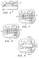
- FIG. 1illustrates a simplified top view of a micro-electro-mechanical device 10
- FIG. 2illustrates a cross-sectional view of micro-electro-mechanical device 10, taken along a cross-sectional line 2-2 in FIG. 1
- FIG. 3illustrates a cross-sectional view of micro-electro-mechanical device 10, taken along a cross-sectional line 3-3 in FIG. 1.
- a substrate 32provides structural or mechanical support.
- substrate 32is comprised of material, such as a high resistivity silicon (Si), gallium arsenide (GaAs), or glass, that does not allow any RF losses. Other materials may also be suitable.
- a first electrically conductive layer or first input/output signal line 34(FIGs. 1 and 3) and a second electrically conductive layer or second input/output signal line 36, a ground electrode 38 (FIG. 2), and a top contact 39 (FIGs. 1 and 3) are formed over substrate 32.
- First input/output signal line 34is physically separated from second input/output signal line 36, as shown in FIG. 1.
- first input/output signal line 34, second input/output signal line 36, ground electrode 38, and top contact 39 for top electrode 46are formed of the same material(s) and at the same time.
- These contact layers or electrodescan be formed by lift off techniques, by electroplating, or by first forming and then patterning a metal layer or metal layers over substrate 32. A lift-off process is preferred if the metal materials used are difficult to pattern using etching techniques.
- the methods of forming the first input/output signal line 34, second input/output signal line 36, ground electrode 38, and top contact 39are well known in the art.
- First input/output signal line 34, second input/output signal line 36, ground electrode 38, and top contact 39are preferably comprised of (1) a conductive layer that is comprised of a non-oxidizing metal or (2) metal layers, such as, for example, chrome and gold (with chrome being deposited first). If chrome and gold are used, a suitable thickness of chrome is 10-30 nanometers and of gold is 0.5-3 micrometers.
- a cantilever structure 44is formed overlying substrate 32 and anchored to substrate 32 at a first or anchored end 48 over top contact 39. Anchored end 48 is fixed to and immovable relative to first input/output signal line 34. Cantilever structure 44 also has a second or moveable end 49 suspended over substrate 32. Moveable end 49 of cantilever structure 44 is moveable in the direction of arrow 50 (FIGs. 2 and 3) and relative to second input/output signal line 36 and substrate 32.
- a shorting bar 40is coupled to the bottom of movable end 49 of cantilever structure 44.
- a first or electrically coupled portion 42 of shorting bar 40is electrically coupled, preferably permanently, to first input/output signal line 34 (see FIG. 2).
- a second or electrically uncoupled portion 43 of shorting bar 40is suspended over and overlies second input/output signal line 36.
- This single contact designis configured so that preferably only the electrically uncoupled portion 43 of shorting bar 40 must be actuated to make electrical contact to second input/output signal line 36.
- This single-point, electrical coupling methodprovides lower total contact resistance than the dual-point electrical coupling method of the prior art.
- shorting bar 40bridges over at least a portion of second input/output signal line 36 and that the electrically coupled portion 42 of shorting bar 40 is permanently electrically coupled to first input/output signal line 34.
- a top electrode 46is formed over the top of cantilever structure 44. Top electrode 46 is electrically coupled to top contact 39. Shorting bar 40 also extends, from electrically coupled portion 42 to electrically uncoupled portion 43, in a direction approximately 90 degrees from the direction of cantilever structure 44.
- electrically coupled portion 42is also physically directly coupled or connected to first input/output signal line 34.
- ground electrode 38is not shown in FIG. 1 (nor will it be shown in the later drawing figures showing a top view) in order to simplify the illustration.
- FIG. 3readily shows the electrically coupled portion 42, which is preferably permanently electrically coupled to first input/output signal line 34, and the electrically uncoupled portion 43, which is overlying, but not electrically coupled to, second input/output signal line 36 when cantilever structure 44 has not been actuated.
- electrically coupled portion 42can also be referred to as a fixed portion
- electrically uncoupled portion 43can also be referred to as a moveable portion.
- Electrically uncoupled portion 43 of shorting bar 40is electrically coupled to second input/output signal line 36 when cantilever structure 44 has been actuated. This actuation preferably only occurs during operation of micro-electro-mechanical device 10.
- Cantilever structure 44is actuated when an electrostatic charge between top electrode 46 and ground electrode 38 pulls the cantilever structure 44 toward ground electrode 38, thus making the second or electrically uncoupled portion 43 of shorting bar 40 be electrically coupled to second input/output signal line 36.
- the electrostatic chargeis formed when a voltage is applied between top electrode 46 and ground electrode 38.
- Cantilever structure 44, shorting bar 40, and top electrode 46are suspended over substrate 32 by first forming a sacrificial layer (not shown) over substrate 32.
- a sacrificial layer(not shown) over substrate 32.
- the formation of a sacrificial layeris well known in the art, and thus is not described herein.
- Shorting bar 40is formed over the sacrificial layer overlying input/output signal lines 34 and 36. Shorting bar 40 is preferably formed using lift-off techniques. Lift-off techniques are well known in the art, and thus this step is not described further. Shorting bar 40 should be comprised of an electrically conductive layer or metal that is compatible with first input/output signal line 34 and second input/output signal line 36. In a preferred embodiment, shorting bar 40 is comprised of a layer of gold and a layer of chrome. Gold is formed first so that the gold of shorting bar 40 is in contact with the gold of first input/output signal line 34 and second input/output signal line 36 when cantilever structure 44 is actuated or closed during switch operation. A suitable amount of gold is approximately 400 - 2,000 nanometers, and a suitable amount of chrome is approximately 15 - 25 nanometers. Other thicknesses, however, may be acceptable.
- the cantilever structure 44is formed over substrate 32 and overlying shorting bar 40.
- An opening (not shown) leading to top contact 39is made in the sacrificial layer (not shown) that is subsequently removed so that cantilever structure 44 can be anchored to it.
- Cantilever structure 44is preferably comprised of silicon dioxide, silicon oxynitride, or silicon nitride, but other dielectrics may be used as well, including a composite layer of different dielectrics.
- the thickness of cantilever structure 44is in the range of approximately 1-3 micrometers and preferably formed by Pressure Enhanced Chemical Vapor Deposition (PECVD) to produce a low stress dielectric layer.
- PECVDPressure Enhanced Chemical Vapor Deposition
- Top electrode 46is then formed over cantilever structure 44 and over top contact 39.
- Top electrode 46is preferably comprised of titanium and gold. For example, 15 - 25 nanometers of titanium and 100 - 300 nanometers of gold may be formed.
- Top electrode 46is preferably formed by using photoresist lift-off techniques.
- Top electrode 46 and cantilever structure 44are defined; then the sacrificial layer is removed from underneath electrically uncoupled portion 43 of shorting bar 40, cantilever structure 44, and top electrode 46 so that electrically uncoupled portion 43, cantilever structure 44, and top electrode 46 are released and are able to move in the direction shown by arrow 50 in FIGs. 2 and 3.
- Micro-electro-mechanical device 10has improved manufacturability and reliability and reduced contact resistance.
- the contact resistance between the first or electrically coupled portion 42 and first input/output signal line 34is lower than the contact resistance between the second or electrically uncoupled portion 43 and second input/output signal line 36.
- the reason that the contact resistance between the first or electrically coupled portion 42 and first input/output signal line 34 is loweris because electrically coupled portion 42 is fixedly or permanently electrically coupled or contacted to first input/output signal line 34.
- micro-electro-mechanical device 10has lower contact resistance overall, which improves the operating characteristics. Manufacturability is improved because the design of a single contact is less complicated than a dual contact design of the prior art (described below).
- FIG. 4illustrates a prior art structure shown in the same view as FIG. 3.
- the same reference numbersare used for similar elements despite their potentially dissimilar configuration, in order to ease the understanding of the differences between micro-electro-mechanical device 10 and the prior art.
- shorting bar 40does not have an electrically coupled portion 42 in combination with an electrically uncoupled portion 43.
- no portion of shorting bar 40is electrically coupled to either of first and second input/output signal lines 34 and 36 until the cantilever structure 44 is actuated.
- FIG. 5shows a simplified top view of a second embodiment of the present invention, which illustrates a cantilever structure 44 having a two finger pattern.
- FIG. 6illustrates a cross-sectional view of the device in FIG. 5, taken along a cross-sectional line 6-6 in FIG. 5.
- the two finger patternallows for the ability to make one of the fingers, or the finger on the side of the electrically uncoupled portion 43 of shorting bar 40, wider (or otherwise having more mass) than the other finger, or the finger on the side of the electrically coupled portion 42 of shorting bar 40.
- more than two fingersmay be formed if desired. With more mass, less electrostatic force is needed to pull the electrically uncoupled portion 43 of shorting bar 40 toward second input/output signal line 36.
- FIG. 7illustrates a third embodiment of the present invention, wherein another design of cantilever structure 44 has a two finger pattern and also provides for more mass on the side of the electrically uncoupled portion 43 of shorting bar 40 is illustrated.
- the overall objectiveis to get more mass on one side, and the openings 51 and 54 are on technique for achieving that.
- cantilever structure 44has more openings 51 on the side of the electrically coupled portion 42 of shorting bar 40. Only two variations have been shown herein, but many different patterns of cantilever structure 44 are available to meet the goal of providing more mass on the side of the electrically uncoupled portion 43 of shorting bar 40.
- Having more mass in cantilever structure 44 on the side of the electrically uncoupled portion 43 of shorting bar 40may provide for higher rigidity, thus higher resistance to deformation of that portion 43 of shorting bar 40, so that portion 43 of shorting bar 40 preferably only bends as needed to make electrical contact with second input/output signal line 36.
- the higher rigiditycompensates for the non-symmetrical bending of the shorting bar 40.
- FIG. 8illustrates a top view of a fourth embodiment of the present invention.
- top electrode 46comprises less metal, or another electrically conductive material, and covers less area of cantilever structure 44, which comprises a two finger pattern, on the side of the electrically uncoupled portion 43 of shorting bar 40.
- the less metal of top electrode 46provides for reduced electrostatic force on the side of the electrically uncoupled portion 43.
- the goalis also to compensate for the asymmetrical bending and improve contact quality.
- FIG. 9illustrates a simplified top view of a fifth embodiment of the present invention
- FIG. 10illustrates a cross-sectional view of micro-electro-mechanical device 10 of FIG. 9 taken along a cross-sectional line 10-10 in FIG. 9.
- shorting bar 40is fabricated to have a symmetrical design when viewed across a width of cantilever structure 44, shown by arrow 52 in FIG. 9 and as shown in FIG. 10, where a length of cantilever structure 44 is greater than the width and a thickness of cantilever structure 44. This symmetry is contrasted to the embodiments shown in FIGs.
- shorting bar 40is asymmetrical across the width of cantilever structure 44.
- electrically coupled portion 42is still fixed, and electrically uncoupled portion 43 is still moveable in a direction of arrow 50 (FIG. 10).
- Shorting bar 40further comprises a third or fixed portion 58 (FIG. 10) permanently and physically connected or coupled to substrate 32 and is not moveable relative to substrate 32.
- Fixed portion 58 (FIG. 10) of shorting bar 40is also an electrically uncoupled portion.
- FIG. 11illustrates a simplified top view of a sixth embodiment of the present invention
- FIG. 12illustrates a cross-sectional view of micro-electro-mechanical device 10 taken along a cross-sectional line 12-12 in FIG. 11.
- One end (in this embodiment, portion 43) of shorting bar 40is formed underneath cantilever structure 44.
- Shorting bar 40also extends, from electrically coupled portion 42 to electrically uncoupled portion 43, in a direction approximately 180 degrees from the direction of cantilever structure 44.
- the electrically coupled portion 42 of the shorting bar 40is also preferably permanently electrically coupled to first input/output signal line 34.
- Electrically uncoupled portion 43 of shorting bar 40is formed underneath the end of the movable end, or end 49, of cantilever structure 44 and overlies second input/output signal line 36.
- the electrically uncoupled portion 43needs to be moved to be electrically coupled to second input/output signal line 36, while the other portion, electrically coupled portion 42, is preferably permanently electrically coupled to first input/output signal line 34.
- shorting bar 40is symmetrical about a length of cantilever structure 44, and a length of shorting bar 40 is substantially parallel to the length of cantilever structure 44
Landscapes
- Micromachines (AREA)
Description
- This invention relates to electronics, in general, and to micro-electro-mechanical devices and methods of making, in particular.
- Micro-electro-mechanical devices are used for a wide range of applications. These devices or micro-switches have the advantage of providing superior switching characteristics over a wide range of frequencies. One type of micro-electro-mechanical switch structure utilizes a cantilever beam design. A cantilever beam with contact metal thereon rests above an input signal line and an output signal line. During switch operation, the beam is electro-statically actuated by applying voltage to an electrode on the cantilever beam. Electrostatic force pulls the cantilever beam toward the input signal line and the output signal line, thus creating a conduction path between the input line and the output line through the metal contact on the cantilever beam.
- One disadvantage of this design is the high contact resistance of the shorting bar, which must make contact to two places, the input signal line and the output signal line. High contact resistance results in higher radio frequency (RF) power insertion loss through the signal path.
- US 5, 258, 591A discloses an apparatus for providing an electrostatically actuated mechanical switch utilizing a cantilever beam element, which is completely conductive.
- Accordingly, a need exists for a micro-electro-mechanical device with reliable mechanical and electrical contact characteristics having low contact resistance. Independent claim 1 discloses such a micro-electro-mechanical device. A need also exists for a method of making the micro-electro-mechanical device.
- The invention will be better understood from a reading of the following detailed description, taken in conjunction with the accompanying figures in the drawings in which:
- FIG. 1 illustrates a simplified top view of a micro-electro-mechanical device according to a first embodiment of the present invention;
- FIG. 2 illustrates a cross-sectional view of the micro-electro-mechanical device of FIG. 1, taken along a cross-sectional line 2-2 in FIG. 1;
- FIG. 3 illustrates a cross-sectional view of the micro-electro-mechanical device of FIG. 1, taken along a cross-sectional line 3-3 in FIG. 1;
- FIG. 4 illustrates a cross-sectional view of a prior art device;
- FIG. 5 illustrates a simplified top view of a micro-electro-mechanical device according to a second embodiment of the present invention;
- FIG. 6 illustrates a cross-sectional view of the micro-electro-mechanical device of FIG. 5, taken along a cross-sectional line 6-6 in FIG. 5;
- FIG. 7 illustrates a simplified top view of a micro-electro-mechanical device according to a third embodiment of the present invention;
- FIG. 8 illustrates a simplified top view of a micro-electro-mechanical device according to a fourth embodiment of the present invention;
- FIG. 9 illustrates a simplified top view of a micro-electro-mechanical device according to a fifth embodiment of the present invention.
- FIG. 10 illustrates a cross-sectional view of the micro-electro-mechanical device of FIG. 9, taken along a cross-sectional line 10-10 in FIG. 9;
- FIG. 11 illustrates a simplified top view of a micro-electro-mechanical device according to a sixth embodiment of the present invention; and
- FIG. 12 illustrates a cross-sectional view of the micro-electro-mechanical device of FIG. 11, taken along a cross-sectional line 12-12 in FIG. 11.
- For simplicity and clarity of illustration, the drawing figures illustrate the general manner of construction, and descriptions and details of well-known features and techniques are omitted to avoid unnecessarily obscuring the invention. Additionally, elements in the drawing figures are not necessarily drawn to scale. For example, the dimensions of some of the elements in the figures may be exaggerated relative to other elements to help to improve understanding of embodiments of the present invention. Furthermore, the same reference numerals in different figures denote the same elements.
- Furthermore, the terms first, second, third, fourth, and the like in the description and in the claims, if any, are used for distinguishing between similar elements and not necessarily for describing a sequential or chronological order. It is further understood that the terms so used are interchangeable under appropriate circumstances such that the embodiments of the invention described herein are, for example, capable of operation in other sequences than illustrated or otherwise described herein.
- Moreover, the terms left, right, front, back, top, bottom, over, under, and the like in the description and in the claims, if any, are used for descriptive purposes and not necessarily for describing permanent relative positions. It is understood that the terms so used are interchangeable under appropriate circumstances such that the embodiments of the invention described herein are, for example, capable of operation in other orientations than illustrated or otherwise described herein.
- The present invention relates to structures and methods for forming a micro-electro-mechanical device. More particularly, the micro-electro-mechanical device described herein utilizes an electrically coupled or fixed portion and an electrically uncoupled or moveable portion of a shorting bar so that when a cantilever structure or beam is actuated, preferably only one portion of the shorting bar,i.e., the uncoupled or movable portion, needs to make electrical contact to one of the input/output signal lines. The electrically coupled or fixed portion of the shorting bar is fabricated so that it is electrically coupled to one of the input/output signal lines preferably at all times, not just during actuation of the cantilever structure.
- Turning now to FIGs. 1, 2, and 3, a micro-electro-
mechanical device 10 is illustrated according to an embodiment of the present invention. FIG. 1 illustrates a simplified top view of a micro-electro-mechanical device 10; FIG. 2 illustrates a cross-sectional view of micro-electro-mechanical device 10, taken along a cross-sectional line 2-2 in FIG. 1, and FIG. 3 illustrates a cross-sectional view of micro-electro-mechanical device 10, taken along a cross-sectional line 3-3 in FIG. 1. Asubstrate 32 provides structural or mechanical support. Preferably,substrate 32 is comprised of material, such as a high resistivity silicon (Si), gallium arsenide (GaAs), or glass, that does not allow any RF losses. Other materials may also be suitable. - A first electrically conductive layer or first input/output signal line 34 (FIGs. 1 and 3) and a second electrically conductive layer or second input/
output signal line 36, a ground electrode 38 (FIG. 2), and a top contact 39 (FIGs. 1 and 3) are formed oversubstrate 32. First input/output signal line 34 is physically separated from second input/output signal line 36, as shown in FIG. 1. - Preferably, first input/
output signal line 34, second input/output signal line 36,ground electrode 38, andtop contact 39 fortop electrode 46 are formed of the same material(s) and at the same time. These contact layers or electrodes can be formed by lift off techniques, by electroplating, or by first forming and then patterning a metal layer or metal layers oversubstrate 32. A lift-off process is preferred if the metal materials used are difficult to pattern using etching techniques. The methods of forming the first input/output signal line 34, second input/output signal line 36,ground electrode 38, andtop contact 39 are well known in the art. - First input/
output signal line 34, second input/output signal line 36,ground electrode 38, andtop contact 39 are preferably comprised of (1) a conductive layer that is comprised of a non-oxidizing metal or (2) metal layers, such as, for example, chrome and gold (with chrome being deposited first). If chrome and gold are used, a suitable thickness of chrome is 10-30 nanometers and of gold is 0.5-3 micrometers. - A
cantilever structure 44 is formed overlyingsubstrate 32 and anchored tosubstrate 32 at a first or anchoredend 48 overtop contact 39. Anchoredend 48 is fixed to and immovable relative to first input/output signal line 34.Cantilever structure 44 also has a second ormoveable end 49 suspended oversubstrate 32.Moveable end 49 ofcantilever structure 44 is moveable in the direction of arrow 50 (FIGs. 2 and 3) and relative to second input/output signal line 36 andsubstrate 32. - A
shorting bar 40 is coupled to the bottom ofmovable end 49 ofcantilever structure 44. A first or electrically coupledportion 42 of shortingbar 40 is electrically coupled, preferably permanently, to first input/output signal line 34 (see FIG. 2). A second or electricallyuncoupled portion 43 of shortingbar 40 is suspended over and overlies second input/output signal line 36. This single contact design is configured so that preferably only the electricallyuncoupled portion 43 of shortingbar 40 must be actuated to make electrical contact to second input/output signal line 36. This single-point, electrical coupling method provides lower total contact resistance than the dual-point electrical coupling method of the prior art. - In FIGs. 1, 2, and 3 one can see that shorting
bar 40 bridges over at least a portion of second input/output signal line 36 and that the electrically coupledportion 42 of shortingbar 40 is permanently electrically coupled to first input/output signal line 34. Atop electrode 46 is formed over the top ofcantilever structure 44.Top electrode 46 is electrically coupled totop contact 39. Shortingbar 40 also extends, from electrically coupledportion 42 to electrically uncoupledportion 43, in a direction approximately 90 degrees from the direction ofcantilever structure 44. - In a preferred embodiment, electrically coupled
portion 42 is also physically directly coupled or connected to first input/output signal line 34. Note thatground electrode 38 is not shown in FIG. 1 (nor will it be shown in the later drawing figures showing a top view) in order to simplify the illustration. - FIG. 3 readily shows the electrically coupled
portion 42, which is preferably permanently electrically coupled to first input/output signal line 34, and the electrically uncoupledportion 43, which is overlying, but not electrically coupled to, second input/output signal line 36 whencantilever structure 44 has not been actuated. In this embodiment, electrically coupledportion 42 can also be referred to as a fixed portion, and electrically uncoupledportion 43 can also be referred to as a moveable portion. - Electrically uncoupled
portion 43 of shortingbar 40 is electrically coupled to second input/output signal line 36 whencantilever structure 44 has been actuated. This actuation preferably only occurs during operation of micro-electro-mechanical device 10.Cantilever structure 44 is actuated when an electrostatic charge betweentop electrode 46 andground electrode 38 pulls thecantilever structure 44 towardground electrode 38, thus making the second or electrically uncoupledportion 43 of shortingbar 40 be electrically coupled to second input/output signal line 36. The electrostatic charge is formed when a voltage is applied betweentop electrode 46 andground electrode 38. - Still referring to FIGs. 1, 2, and 3, the process of forming
cantilever structure 44, shortingbar 40, andtop electrode 46 is described briefly below.Cantilever structure 44, shortingbar 40, andtop electrode 46 are suspended oversubstrate 32 by first forming a sacrificial layer (not shown) oversubstrate 32. The formation of a sacrificial layer is well known in the art, and thus is not described herein. - Shorting
bar 40 is formed over the sacrificial layer overlying input/output signal lines bar 40 is preferably formed using lift-off techniques. Lift-off techniques are well known in the art, and thus this step is not described further. Shortingbar 40 should be comprised of an electrically conductive layer or metal that is compatible with first input/output signal line 34 and second input/output signal line 36. In a preferred embodiment, shortingbar 40 is comprised of a layer of gold and a layer of chrome. Gold is formed first so that the gold of shortingbar 40 is in contact with the gold of first input/output signal line 34 and second input/output signal line 36 whencantilever structure 44 is actuated or closed during switch operation. A suitable amount of gold is approximately 400 - 2,000 nanometers, and a suitable amount of chrome is approximately 15 - 25 nanometers. Other thicknesses, however, may be acceptable. - Subsequent to the formation of shorting
bar 40 and before removal of the sacrificial layer (not shown), thecantilever structure 44 is formed oversubstrate 32 andoverlying shorting bar 40. An opening (not shown) leading totop contact 39 is made in the sacrificial layer (not shown) that is subsequently removed so thatcantilever structure 44 can be anchored to it.Cantilever structure 44 is preferably comprised of silicon dioxide, silicon oxynitride, or silicon nitride, but other dielectrics may be used as well, including a composite layer of different dielectrics. The thickness ofcantilever structure 44 is in the range of approximately 1-3 micrometers and preferably formed by Pressure Enhanced Chemical Vapor Deposition (PECVD) to produce a low stress dielectric layer. Top electrode 46 is then formed overcantilever structure 44 and overtop contact 39.Top electrode 46 is preferably comprised of titanium and gold. For example, 15 - 25 nanometers of titanium and 100 - 300 nanometers of gold may be formed.Top electrode 46 is preferably formed by using photoresist lift-off techniques.Top electrode 46 andcantilever structure 44 are defined; then the sacrificial layer is removed from underneath electrically uncoupledportion 43 of shortingbar 40,cantilever structure 44, andtop electrode 46 so that electrically uncoupledportion 43,cantilever structure 44, andtop electrode 46 are released and are able to move in the direction shown byarrow 50 in FIGs. 2 and 3.- Micro-electro-
mechanical device 10 has improved manufacturability and reliability and reduced contact resistance. Whencantilever structure 44 is actuated, the contact resistance between the first or electrically coupledportion 42 and first input/output signal line 34 is lower than the contact resistance between the second or electrically uncoupledportion 43 and second input/output signal line 36. The reason that the contact resistance between the first or electrically coupledportion 42 and first input/output signal line 34 is lower is because electrically coupledportion 42 is fixedly or permanently electrically coupled or contacted to first input/output signal line 34. Thus, micro-electro-mechanical device 10 has lower contact resistance overall, which improves the operating characteristics. Manufacturability is improved because the design of a single contact is less complicated than a dual contact design of the prior art (described below). - FIG. 4 illustrates a prior art structure shown in the same view as FIG. 3. The same reference numbers are used for similar elements despite their potentially dissimilar configuration, in order to ease the understanding of the differences between micro-electro-
mechanical device 10 and the prior art. In the prior art, shortingbar 40 does not have an electrically coupledportion 42 in combination with an electrically uncoupledportion 43. In the illustrated prior art, no portion of shortingbar 40 is electrically coupled to either of first and second input/output signal lines cantilever structure 44 is actuated. - FIG. 5 shows a simplified top view of a second embodiment of the present invention, which illustrates a
cantilever structure 44 having a two finger pattern. FIG. 6 illustrates a cross-sectional view of the device in FIG. 5, taken along a cross-sectional line 6-6 in FIG. 5. For ease of understanding, the same numerals are used for similar elements, despite their potentially dissimilar configurations. The two finger pattern allows for the ability to make one of the fingers, or the finger on the side of the electrically uncoupledportion 43 of shortingbar 40, wider (or otherwise having more mass) than the other finger, or the finger on the side of the electrically coupledportion 42 of shortingbar 40. Although not illustrated herein, more than two fingers may be formed if desired. With more mass, less electrostatic force is needed to pull the electrically uncoupledportion 43 of shortingbar 40 toward second input/output signal line 36. - FIG. 7 illustrates a third embodiment of the present invention, wherein another design of
cantilever structure 44 has a two finger pattern and also provides for more mass on the side of the electrically uncoupledportion 43 of shortingbar 40 is illustrated. The overall objective is to get more mass on one side, and theopenings cantilever structure 44 hasmore openings 51 on the side of the electrically coupledportion 42 of shortingbar 40. Only two variations have been shown herein, but many different patterns ofcantilever structure 44 are available to meet the goal of providing more mass on the side of the electrically uncoupledportion 43 of shortingbar 40. Having more mass incantilever structure 44 on the side of the electrically uncoupledportion 43 of shortingbar 40 may provide for higher rigidity, thus higher resistance to deformation of thatportion 43 of shortingbar 40, so thatportion 43 of shortingbar 40 preferably only bends as needed to make electrical contact with second input/output signal line 36. The higher rigidity compensates for the non-symmetrical bending of the shortingbar 40. - FIG. 8 illustrates a top view of a fourth embodiment of the present invention. For ease of understanding, the same numerals are used for similar elements, despite their potentially dissimilar configurations. In this embodiment,
top electrode 46 comprises less metal, or another electrically conductive material, and covers less area ofcantilever structure 44, which comprises a two finger pattern, on the side of the electrically uncoupledportion 43 of shortingbar 40. The less metal oftop electrode 46 provides for reduced electrostatic force on the side of the electrically uncoupledportion 43. The goal is also to compensate for the asymmetrical bending and improve contact quality. - Now with reference to both FIGs. 9 and 10, FIG. 9 illustrates a simplified top view of a fifth embodiment of the present invention, and FIG. 10 illustrates a cross-sectional view of micro-electro-
mechanical device 10 of FIG. 9 taken along a cross-sectional line 10-10 in FIG. 9. For ease of understanding, the same numerals are used for similar elements, despite their potentially dissimilar configurations. In this embodiment, shortingbar 40 is fabricated to have a symmetrical design when viewed across a width ofcantilever structure 44, shown byarrow 52 in FIG. 9 and as shown in FIG. 10, where a length ofcantilever structure 44 is greater than the width and a thickness ofcantilever structure 44. This symmetry is contrasted to the embodiments shown in FIGs. 1, 3, 5, 6, 7, and 8 in which shortingbar 40 is asymmetrical across the width ofcantilever structure 44. In this embodiment, electrically coupledportion 42 is still fixed, and electrically uncoupledportion 43 is still moveable in a direction of arrow 50 (FIG. 10). Shortingbar 40, however, further comprises a third or fixed portion 58 (FIG. 10) permanently and physically connected or coupled tosubstrate 32 and is not moveable relative tosubstrate 32. Fixed portion 58 (FIG. 10) of shortingbar 40 is also an electrically uncoupled portion. - Referring to FIGs. 11 and 12, FIG. 11 illustrates a simplified top view of a sixth embodiment of the present invention, and FIG. 12 illustrates a cross-sectional view of micro-electro-
mechanical device 10 taken along a cross-sectional line 12-12 in FIG. 11. For ease of understanding, the same numerals are used for similar elements, despite their potentially dissimilar configurations. One end (in this embodiment, portion 43) of shortingbar 40 is formed underneathcantilever structure 44. Shortingbar 40 also extends, from electrically coupledportion 42 to electrically uncoupledportion 43, in a direction approximately 180 degrees from the direction ofcantilever structure 44. - In the embodiment of FIGs. 11 and 12, the electrically coupled
portion 42 of the shortingbar 40 is also preferably permanently electrically coupled to first input/output signal line 34. Electrically uncoupledportion 43 of shortingbar 40 is formed underneath the end of the movable end, or end 49, ofcantilever structure 44 and overlies second input/output signal line 36. In this embodiment, as in the other embodiments of the present invention, preferably only one portion, the electrically uncoupledportion 43, needs to be moved to be electrically coupled to second input/output signal line 36, while the other portion, electrically coupledportion 42, is preferably permanently electrically coupled to first input/output signal line 34. Also in this embodiment, shortingbar 40 is symmetrical about a length ofcantilever structure 44, and a length of shortingbar 40 is substantially parallel to the length ofcantilever structure 44 - By now it should be appreciated that structures and methods have been provided for improving the manufacturability of micro-electro-mechanical devices as well as for providing a micro-electro-mechanical device with improved electrical characteristics and better reliability. In particular, the aforementioned advantages are obtained by a shorting
bar 40 that is electrically coupled to one first input/output signal line 34, preferably at all times during operation, so that electrical coupling preferably only needs to be made to the other second input/output signal line 36 during operation. Thus, a design and process for fabricating a micro-electro-mechanical device, which fully meets the advantages set forth above, has been provided. - Although the invention has been described with reference to specific embodiments, it will be understood by those skilled in the art that various changes may be made without departing from the scope of the invention. For instance, the numerous details set forth herein such as, for example, the material compositions are provided to facilitate the understanding of the invention and are not provided to limit the scope of the invention. Accordingly, the disclosure of embodiments of the invention is intended to be illustrative of the scope of the invention and is not intended to be limiting. It is intended that the scope of the invention shall be limited only to the extent required by the appended claims.
- Additionally, benefits, other advantages, and solutions to problems have been described with regard to specific embodiments. The benefits, advantages, solutions to problems, and any element or elements that may cause any benefit, advantage, or solution to occur or become more pronounced, however, are not to be construed as critical, required, or essential features or elements of any or all of the claims.
Claims (11)
- A micro-electro-mechanical device (10) comprising:a substrate (32);a first conductive layer (34) over the substrate;a second conductive layer (36) over the substrate and separated from the first conductive layer; anda cantilever structure (44) over the substrate, wherein the cantilever structure has a first end (48) anchored to the substrate and a second end (49) suspended over the substrate;wherein the micro-electro-mechanical device (10) ischaracterised in that the cantilever structure (44) comprises a dielectric and further wherein a top electrode is formed over the cantilever structure (44); anda shorting bar (40) adjacent to the cantilever structure proximate the second end of the cantilever structure on a underside of the cantilever structure opposite to the top electrode, wherein the shorting bar (40) has a first portion and a second portion, and wherein the first portion is anchored to and electrically coupled to the first conductive layer and the second portion overlies and is removably electrically coupled to the second conductive layer, wherein responsive to applying an electrostatic charge between the top electrode and a underlying ground electrode, the cantilever structure (44) pulls toward the underlying ground electrode and makes the second portion of the shorting bar (40) electrically couple to the second conductive layer (36).
- The micro-electro-mechanical device (10) of claim 1 wherein the cantilever structure has less mass at a first side of the cantilever structure than at a second side of the cantilever structure, the first side of the cantilever structure closer to the first conductive layer than the second side of the cantilever structure.
- The micro-electro-mechanical device of claim 1 further comprising:a third conductive layer over the cantilever structure and covering more area at a first side of the cantilever structure than at a second side of the cantilever structure, the first side of the cantilever structure closer to the first conductive layer than the second side of the cantilever structure.
- The micro-electro-mechanical device of claim 1 wherein the cantilever structure has first and second fingers over the second conductive layer, the first finger closer to the first conductive layer than the second finger and narrower than the second finger.
- The micro-electro-mechanical device of claim 1 wherein the cantilever structure has less mass at a first side of the cantilever structure than at a second side of the cantilever structure, the first side closer to the first conductive layer than the second side.
- The micro-electro-mechanical device of claim 1 wherein a third portion of shorting bar is anchored to the substrate, the second portion of the shorting bar located between the first and third portions of the shorting bar.
- The micro-electro-mechanical device of claim 1 wherein the shorting bar is symmetrical across a width of the cantilever structure.
- The micro-electro-mechanical device of claim 1 wherein the shorting bar is asymmetric across a width of the cantilever structure.
- The micro-electro-mechanical device of claim 1 wherein the cantilever structure has a length substantially parallel to a length of the shorting bar.
- The micro-electro-mechanical device of claim 1 wherein the shorting bar extends in a direction approximately 180 degrees from a direction of the cantilever structure.
- The micro-electro-mechanical device of claim 1 wherein the shorting bar extends in a direction approximately 90 degrees from a direction of the cantilever structure.
Applications Claiming Priority (2)
| Application Number | Priority Date | Filing Date | Title |
|---|---|---|---|
| US159909 | 1998-09-24 | ||
| US10/159,909US6794101B2 (en) | 2002-05-31 | 2002-05-31 | Micro-electro-mechanical device and method of making |
Publications (2)
| Publication Number | Publication Date |
|---|---|
| EP1367615A1 EP1367615A1 (en) | 2003-12-03 |
| EP1367615B1true EP1367615B1 (en) | 2006-08-16 |
Family
ID=29419717
Family Applications (1)
| Application Number | Title | Priority Date | Filing Date |
|---|---|---|---|
| EP03011707AExpired - LifetimeEP1367615B1 (en) | 2002-05-31 | 2003-05-23 | Micro-electro-mechanical device and method of making |
Country Status (3)
| Country | Link |
|---|---|
| US (1) | US6794101B2 (en) |
| EP (1) | EP1367615B1 (en) |
| DE (1) | DE60307539T2 (en) |
Families Citing this family (32)
| Publication number | Priority date | Publication date | Assignee | Title |
|---|---|---|---|---|
| JP4206856B2 (en)* | 2002-07-30 | 2009-01-14 | パナソニック株式会社 | Switch and switch manufacturing method |
| KR100513723B1 (en)* | 2002-11-18 | 2005-09-08 | 삼성전자주식회사 | MicroElectro Mechanical system switch |
| US8732644B1 (en) | 2003-09-15 | 2014-05-20 | Nvidia Corporation | Micro electro mechanical switch system and method for testing and configuring semiconductor functional circuits |
| US8775997B2 (en) | 2003-09-15 | 2014-07-08 | Nvidia Corporation | System and method for testing and configuring semiconductor functional circuits |
| US8872833B2 (en) | 2003-09-15 | 2014-10-28 | Nvidia Corporation | Integrated circuit configuration system and method |
| US6880940B1 (en)* | 2003-11-10 | 2005-04-19 | Honda Motor Co., Ltd. | Magnesium mirror base with countermeasures for galvanic corrosion |
| US8711161B1 (en) | 2003-12-18 | 2014-04-29 | Nvidia Corporation | Functional component compensation reconfiguration system and method |
| FR2868591B1 (en)* | 2004-04-06 | 2006-06-09 | Commissariat Energie Atomique | MICROCOMMUTER WITH LOW ACTUATION VOLTAGE AND LOW CONSUMPTION |
| US8723231B1 (en)* | 2004-09-15 | 2014-05-13 | Nvidia Corporation | Semiconductor die micro electro-mechanical switch management system and method |
| US8711156B1 (en) | 2004-09-30 | 2014-04-29 | Nvidia Corporation | Method and system for remapping processing elements in a pipeline of a graphics processing unit |
| US8021193B1 (en) | 2005-04-25 | 2011-09-20 | Nvidia Corporation | Controlled impedance display adapter |
| US7793029B1 (en) | 2005-05-17 | 2010-09-07 | Nvidia Corporation | Translation device apparatus for configuring printed circuit board connectors |
| US20070040637A1 (en)* | 2005-08-19 | 2007-02-22 | Yee Ian Y K | Microelectromechanical switches having mechanically active components which are electrically isolated from components of the switch used for the transmission of signals |
| US8417838B2 (en) | 2005-12-12 | 2013-04-09 | Nvidia Corporation | System and method for configurable digital communication |
| US8412872B1 (en) | 2005-12-12 | 2013-04-02 | Nvidia Corporation | Configurable GPU and method for graphics processing using a configurable GPU |
| US7556978B2 (en)* | 2006-02-28 | 2009-07-07 | Freescale Semiconductor, Inc. | Piezoelectric MEMS switches and methods of making |
| US7567782B2 (en)* | 2006-07-28 | 2009-07-28 | Freescale Semiconductor, Inc. | Re-configurable impedance matching and harmonic filter system |
| US7586238B2 (en)* | 2006-08-17 | 2009-09-08 | Freescale Semiconductor, Inc. | Control and testing of a micro electromechanical switch having a piezo element |
| US7479785B2 (en) | 2006-08-17 | 2009-01-20 | Freescale Semiconductor, Inc. | Control and testing of a micro electromechanical switch |
| US20080102762A1 (en)* | 2006-10-30 | 2008-05-01 | Lianjun Liu | Methods and apparatus for a hybrid antenna switching system |
| US7674646B2 (en)* | 2006-11-07 | 2010-03-09 | Freescale Semiconductor, Inc. | Three dimensional integrated passive device and method of fabrication |
| US7630693B2 (en)* | 2006-11-16 | 2009-12-08 | Freescale Semiconductor, Inc. | Transmitter with improved power efficiency |
| US7663196B2 (en)* | 2007-02-09 | 2010-02-16 | Freescale Semiconductor, Inc. | Integrated passive device and method of fabrication |
| US7869784B2 (en)* | 2007-02-27 | 2011-01-11 | Freescale Semiconductor, Inc. | Radio frequency circuit with integrated on-chip radio frequency inductive signal coupler |
| US7830066B2 (en) | 2007-07-26 | 2010-11-09 | Freescale Semiconductor, Inc. | Micromechanical device with piezoelectric and electrostatic actuation and method therefor |
| US8724483B2 (en) | 2007-10-22 | 2014-05-13 | Nvidia Corporation | Loopback configuration for bi-directional interfaces |
| US8687639B2 (en)* | 2009-06-04 | 2014-04-01 | Nvidia Corporation | Method and system for ordering posted packets and non-posted packets transfer |
| US8779886B2 (en)* | 2009-11-30 | 2014-07-15 | General Electric Company | Switch structures |
| US9176909B2 (en) | 2009-12-11 | 2015-11-03 | Nvidia Corporation | Aggregating unoccupied PCI-e links to provide greater bandwidth |
| US9331869B2 (en) | 2010-03-04 | 2016-05-03 | Nvidia Corporation | Input/output request packet handling techniques by a device specific kernel mode driver |
| US9330031B2 (en) | 2011-12-09 | 2016-05-03 | Nvidia Corporation | System and method for calibration of serial links using a serial-to-parallel loopback |
| CN118098844B (en)* | 2024-04-22 | 2024-09-13 | 荣耀终端有限公司 | MEMS switch and electronic equipment |
Family Cites Families (13)
| Publication number | Priority date | Publication date | Assignee | Title |
|---|---|---|---|---|
| US5258591A (en)* | 1991-10-18 | 1993-11-02 | Westinghouse Electric Corp. | Low inductance cantilever switch |
| JP3182301B2 (en)* | 1994-11-07 | 2001-07-03 | キヤノン株式会社 | Microstructure and method for forming the same |
| US5578976A (en)* | 1995-06-22 | 1996-11-26 | Rockwell International Corporation | Micro electromechanical RF switch |
| DE19646667C2 (en)* | 1996-11-12 | 1998-11-12 | Fraunhofer Ges Forschung | Method of manufacturing a micromechanical relay |
| US6046659A (en)* | 1998-05-15 | 2000-04-04 | Hughes Electronics Corporation | Design and fabrication of broadband surface-micromachined micro-electro-mechanical switches for microwave and millimeter-wave applications |
| US6100477A (en)* | 1998-07-17 | 2000-08-08 | Texas Instruments Incorporated | Recessed etch RF micro-electro-mechanical switch |
| US6153839A (en)* | 1998-10-22 | 2000-11-28 | Northeastern University | Micromechanical switching devices |
| DE10031569A1 (en)* | 1999-07-01 | 2001-02-01 | Advantest Corp | Highly miniaturized relay in integrated circuit form, providing reliable operation and high isolation at high frequencies, includes see-saw mounted plate alternately closing contacts on substrate when rocked |
| US6310339B1 (en)* | 1999-10-28 | 2001-10-30 | Hrl Laboratories, Llc | Optically controlled MEM switches |
| US6396368B1 (en)* | 1999-11-10 | 2002-05-28 | Hrl Laboratories, Llc | CMOS-compatible MEM switches and method of making |
| US6373007B1 (en)* | 2000-04-19 | 2002-04-16 | The United States Of America As Represented By The Secretary Of The Air Force | Series and shunt mems RF switch |
| EP1156504A3 (en)* | 2000-05-16 | 2003-12-10 | Fraunhofer-Gesellschaft zur Förderung der angewandten Forschung e.V. | Micromechanical relay with improved switching behaviour |
| US6483056B2 (en)* | 2000-10-27 | 2002-11-19 | Daniel J Hyman | Microfabricated relay with multimorph actuator and electrostatic latch mechanism |
- 2002
- 2002-05-31USUS10/159,909patent/US6794101B2/ennot_activeExpired - Lifetime
- 2003
- 2003-05-23EPEP03011707Apatent/EP1367615B1/ennot_activeExpired - Lifetime
- 2003-05-23DEDE60307539Tpatent/DE60307539T2/ennot_activeExpired - Lifetime
Also Published As
| Publication number | Publication date |
|---|---|
| EP1367615A1 (en) | 2003-12-03 |
| DE60307539D1 (en) | 2006-09-28 |
| DE60307539T2 (en) | 2006-12-07 |
| US20030224267A1 (en) | 2003-12-04 |
| US6794101B2 (en) | 2004-09-21 |
Similar Documents
| Publication | Publication Date | Title |
|---|---|---|
| EP1367615B1 (en) | Micro-electro-mechanical device and method of making | |
| US7352266B2 (en) | Head electrode region for a reliable metal-to-metal contact micro-relay MEMS switch | |
| US7675393B2 (en) | MEMS switch | |
| US5258591A (en) | Low inductance cantilever switch | |
| US7053737B2 (en) | Stress bimorph MEMS switches and methods of making same | |
| US7605675B2 (en) | Electromechanical switch with partially rigidified electrode | |
| EP1535297B1 (en) | Diaphragm activated micro-electromechanical switch | |
| US7299538B2 (en) | Method for fabricating micro-electro-mechanical systems | |
| US7515023B2 (en) | Micro-switching device and method of manufacturing micro-switching device | |
| US7212091B2 (en) | Micro-electro-mechanical RF switch | |
| US7022542B2 (en) | Manufacturing method of a microelectromechanical switch | |
| US20050040486A1 (en) | Electrostatic RF MEMS switches | |
| US6962832B2 (en) | Fabrication method for making a planar cantilever, low surface leakage, reproducible and reliable metal dimple contact micro-relay MEMS switch | |
| US7851976B2 (en) | Micro movable device and method of making the same using wet etching | |
| US8279026B2 (en) | Micro-machined relay | |
| US8610520B2 (en) | Electrostatically actuated micro-mechanical switching device | |
| JP2007535797A (en) | Beam for micromachine technology (MEMS) switches | |
| US20190088435A1 (en) | Mems membrane with integrated transmission line | |
| EP1556877B1 (en) | A micromachined relay with inorganic insulation | |
| US7439117B2 (en) | Method for designing a micro electromechanical device with reduced self-actuation | |
| EP1863055B1 (en) | Milimeter wave switches | |
| US7230513B2 (en) | Planarized structure for a reliable metal-to-metal contact micro-relay MEMS switch | |
| EP1675148B1 (en) | Method for designing a micro electromechanical device with reduced self-actuation | |
| WO2024209207A1 (en) | Mems bridge | |
| JP2004214112A (en) | Micro machine switch |
Legal Events
| Date | Code | Title | Description |
|---|---|---|---|
| PUAI | Public reference made under article 153(3) epc to a published international application that has entered the european phase | Free format text:ORIGINAL CODE: 0009012 | |
| AK | Designated contracting states | Kind code of ref document:A1 Designated state(s):AT BE BG CH CY CZ DE DK EE ES FI FR GB GR HU IE IT LI LU MC NL PT RO SE SI SK TR | |
| AX | Request for extension of the european patent | Extension state:AL LT LV MK | |
| 17P | Request for examination filed | Effective date:20040603 | |
| AKX | Designation fees paid | Designated state(s):DE FR GB IT | |
| RAP1 | Party data changed (applicant data changed or rights of an application transferred) | Owner name:FREESCALE SEMICONDUCTOR, INC. | |
| 17Q | First examination report despatched | Effective date:20041102 | |
| GRAP | Despatch of communication of intention to grant a patent | Free format text:ORIGINAL CODE: EPIDOSNIGR1 | |
| GRAS | Grant fee paid | Free format text:ORIGINAL CODE: EPIDOSNIGR3 | |
| GRAA | (expected) grant | Free format text:ORIGINAL CODE: 0009210 | |
| AK | Designated contracting states | Kind code of ref document:B1 Designated state(s):DE FR GB IT | |
| PG25 | Lapsed in a contracting state [announced via postgrant information from national office to epo] | Ref country code:IT Free format text:LAPSE BECAUSE OF FAILURE TO SUBMIT A TRANSLATION OF THE DESCRIPTION OR TO PAY THE FEE WITHIN THE PRESCRIBED TIME-LIMIT;WARNING: LAPSES OF ITALIAN PATENTS WITH EFFECTIVE DATE BEFORE 2007 MAY HAVE OCCURRED AT ANY TIME BEFORE 2007. THE CORRECT EFFECTIVE DATE MAY BE DIFFERENT FROM THE ONE RECORDED. Effective date:20060816 | |
| REG | Reference to a national code | Ref country code:GB Ref legal event code:FG4D | |
| REF | Corresponds to: | Ref document number:60307539 Country of ref document:DE Date of ref document:20060928 Kind code of ref document:P | |
| ET | Fr: translation filed | ||
| PLBE | No opposition filed within time limit | Free format text:ORIGINAL CODE: 0009261 | |
| STAA | Information on the status of an ep patent application or granted ep patent | Free format text:STATUS: NO OPPOSITION FILED WITHIN TIME LIMIT | |
| 26N | No opposition filed | Effective date:20070518 | |
| REG | Reference to a national code | Ref country code:FR Ref legal event code:PLFP Year of fee payment:13 | |
| REG | Reference to a national code | Ref country code:DE Ref legal event code:R082 Ref document number:60307539 Country of ref document:DE Representative=s name:SCHUMACHER & WILLSAU PATENTANWALTSGESELLSCHAFT, DE Ref country code:DE Ref legal event code:R081 Ref document number:60307539 Country of ref document:DE Owner name:NORTH STAR INNOVATIONS INC., COSTA MESA, US Free format text:FORMER OWNER: FREESCALE SEMICONDUCTOR, INC., AUSTIN, TEX., US | |
| REG | Reference to a national code | Ref country code:GB Ref legal event code:732E Free format text:REGISTERED BETWEEN 20160303 AND 20160309 | |
| REG | Reference to a national code | Ref country code:FR Ref legal event code:TP Owner name:NORTH STAR INNOVATIONS INC., US Effective date:20160401 | |
| REG | Reference to a national code | Ref country code:FR Ref legal event code:PLFP Year of fee payment:14 | |
| PGFP | Annual fee paid to national office [announced via postgrant information from national office to epo] | Ref country code:DE Payment date:20160527 Year of fee payment:14 Ref country code:GB Payment date:20160527 Year of fee payment:14 | |
| PGFP | Annual fee paid to national office [announced via postgrant information from national office to epo] | Ref country code:FR Payment date:20160530 Year of fee payment:14 | |
| REG | Reference to a national code | Ref country code:DE Ref legal event code:R119 Ref document number:60307539 Country of ref document:DE | |
| GBPC | Gb: european patent ceased through non-payment of renewal fee | Effective date:20170523 | |
| REG | Reference to a national code | Ref country code:FR Ref legal event code:ST Effective date:20180131 | |
| PG25 | Lapsed in a contracting state [announced via postgrant information from national office to epo] | Ref country code:DE Free format text:LAPSE BECAUSE OF NON-PAYMENT OF DUE FEES Effective date:20171201 Ref country code:GB Free format text:LAPSE BECAUSE OF NON-PAYMENT OF DUE FEES Effective date:20170523 | |
| PG25 | Lapsed in a contracting state [announced via postgrant information from national office to epo] | Ref country code:FR Free format text:LAPSE BECAUSE OF NON-PAYMENT OF DUE FEES Effective date:20170531 |