EP1359402B1 - Pressure sensor - Google Patents
Pressure sensorDownload PDFInfo
- Publication number
- EP1359402B1 EP1359402B1EP02253102.4AEP02253102AEP1359402B1EP 1359402 B1EP1359402 B1EP 1359402B1EP 02253102 AEP02253102 AEP 02253102AEP 1359402 B1EP1359402 B1EP 1359402B1
- Authority
- EP
- European Patent Office
- Prior art keywords
- pressure sensor
- semiconductor material
- pressure
- diaphragm
- electrode
- Prior art date
- Legal status (The legal status is an assumption and is not a legal conclusion. Google has not performed a legal analysis and makes no representation as to the accuracy of the status listed.)
- Expired - Lifetime
Links
- 239000011521glassSubstances0.000claimsdescription25
- 239000000758substrateSubstances0.000claimsdescription22
- 229910052710siliconInorganic materials0.000claimsdescription18
- 239000010703siliconSubstances0.000claimsdescription18
- 239000000463materialSubstances0.000claimsdescription13
- 239000004065semiconductorSubstances0.000claimsdescription12
- 239000004020conductorSubstances0.000claimsdescription11
- 238000009792diffusion processMethods0.000claimsdescription8
- 230000003993interactionEffects0.000claimsdescription2
- 238000005459micromachiningMethods0.000claimsdescription2
- XUIMIQQOPSSXEZ-UHFFFAOYSA-NSiliconChemical compound[Si]XUIMIQQOPSSXEZ-UHFFFAOYSA-N0.000description23
- 239000003990capacitorSubstances0.000description19
- 229910052751metalInorganic materials0.000description12
- 239000002184metalSubstances0.000description12
- 239000010410layerSubstances0.000description10
- 238000004519manufacturing processMethods0.000description8
- 238000000034methodMethods0.000description6
- 238000005259measurementMethods0.000description5
- 238000005530etchingMethods0.000description4
- 239000010409thin filmSubstances0.000description4
- ZOXJGFHDIHLPTG-UHFFFAOYSA-NBoronChemical compound[B]ZOXJGFHDIHLPTG-UHFFFAOYSA-N0.000description2
- 229910052796boronInorganic materials0.000description2
- 238000001514detection methodMethods0.000description2
- 238000001312dry etchingMethods0.000description2
- 238000005516engineering processMethods0.000description2
- 238000002161passivationMethods0.000description2
- 239000002344surface layerSubstances0.000description2
- 239000004411aluminiumSubstances0.000description1
- 229910052782aluminiumInorganic materials0.000description1
- XAGFODPZIPBFFR-UHFFFAOYSA-NaluminiumChemical compound[Al]XAGFODPZIPBFFR-UHFFFAOYSA-N0.000description1
- 230000009286beneficial effectEffects0.000description1
- 230000015572biosynthetic processEffects0.000description1
- 238000006243chemical reactionMethods0.000description1
- 230000000694effectsEffects0.000description1
- BHEPBYXIRTUNPN-UHFFFAOYSA-Nhydridophosphorus(.) (triplet)Chemical compound[PH]BHEPBYXIRTUNPN-UHFFFAOYSA-N0.000description1
- 238000002513implantationMethods0.000description1
- 238000005468ion implantationMethods0.000description1
- 238000002955isolationMethods0.000description1
- 230000007774longtermEffects0.000description1
- 238000001465metallisationMethods0.000description1
- 238000012544monitoring processMethods0.000description1
- 238000004806packaging method and processMethods0.000description1
- 230000035945sensitivityEffects0.000description1
- 238000001039wet etchingMethods0.000description1
Images


Classifications
- G—PHYSICS
- G01—MEASURING; TESTING
- G01L—MEASURING FORCE, STRESS, TORQUE, WORK, MECHANICAL POWER, MECHANICAL EFFICIENCY, OR FLUID PRESSURE
- G01L9/00—Measuring steady of quasi-steady pressure of fluid or fluent solid material by electric or magnetic pressure-sensitive elements; Transmitting or indicating the displacement of mechanical pressure-sensitive elements, used to measure the steady or quasi-steady pressure of a fluid or fluent solid material, by electric or magnetic means
- G01L9/0041—Transmitting or indicating the displacement of flexible diaphragms
- G01L9/0072—Transmitting or indicating the displacement of flexible diaphragms using variations in capacitance
- G01L9/0073—Transmitting or indicating the displacement of flexible diaphragms using variations in capacitance using a semiconductive diaphragm
- H—ELECTRICITY
- H10—SEMICONDUCTOR DEVICES; ELECTRIC SOLID-STATE DEVICES NOT OTHERWISE PROVIDED FOR
- H10D—INORGANIC ELECTRIC SEMICONDUCTOR DEVICES
- H10D48/00—Individual devices not covered by groups H10D1/00 - H10D44/00
- H10D48/50—Devices controlled by mechanical forces, e.g. pressure
- G—PHYSICS
- G01—MEASURING; TESTING
- G01L—MEASURING FORCE, STRESS, TORQUE, WORK, MECHANICAL POWER, MECHANICAL EFFICIENCY, OR FLUID PRESSURE
- G01L19/00—Details of, or accessories for, apparatus for measuring steady or quasi-steady pressure of a fluent medium insofar as such details or accessories are not special to particular types of pressure gauges
- G01L19/06—Means for preventing overload or deleterious influence of the measured medium on the measuring device or vice versa
- G01L19/069—Protection against electromagnetic or electrostatic interferences
Definitions
- Pressure sensorsare extensively used in a large and increasingly varied field, including important areas such as medical instrumentation, automotive applications such as engine control and tyre pressure monitoring, industrial process control and the avionics industry.
- the most commonly used conversion principles for silicon based pressure sensorsare capacitive detection and piezoresistive detection.
- Piezoresistive sensorsare generally considered to be more robust than capacitive sensors. Another advantage is that they give an output signal proportional to the input with good linearity. Capacitive sensors, on the other hand, have the advantage over the piezoresistive type in that they consume less power, but have a non-linear direct output signal and are more sensitive to electromagnetic interference. Capacitive silicon sensors can be made to be small in size and can easily be made by surface micromachinirig. However, they are not very robust and their pressure sensitive diaphragm needs to be protected against the pressure media by a gel or other flexible material in most applications. This results in an increase in vibration sensitivity due to the mass added to the top of the diaphragm. Advanced and well proven methods of manufacturing silicon pressure sensors and inertial sensors are described in the patent publications EP-A-742581 and EP-A-994330 .
- US4390925discloses a method for manufacturing a variable capacitance pressure transducer having a plurality of recesses and interconnecting paths etched into the surface of a silicon wafer. A glass plate having thin-film metal deposits on the surface thereof is electrostatically bonded to the silicon.
- the present inventionseeks to provide a capacitive silicon sensor arrangement for the measurement of pressure that overcomes the above mentioned problems.
- a capacitive-type pressure sensorcomprising:
- the sensorhas a pressure sensitive diaphragm acting as the movable electrode in the capacitor, an on-chip vacuum reference volume preferably sealed by anodic bonding acting as the gap in the capacitor and with the counter electrode of the capacitor on glass. These are connected to the outside of the sealed cavity by a conduction system consisting of metal interconnects on the glass, press contacts between the metal on glass and metal on the silicon part; and with buried conductors in the silicon substrate for crossing of the hermetically sealed cavity to metal interconnects and wire bonding areas outside the sealed area.
- the inventionresults in a robust and reliable pressure sensor with good media compatibility.
- the process technology that is usedresults in low manufacturing cost which is beneficial for high volume applications such as in the automotive industry.
- Higher measurement accuracycan be achieved by incorporating a second and matching capacitor on the same chip as the pressure sensitive capacitor and measuring the relative differences in the two capacitance values.
- the high accuracyis obtained by the good matching and tracking of the zero-point over temperature and time of the two capacitors values due to the near identical effects of packaging stress on the two capacitors.
- This inventionis made possible by using silicon planar processing combined with modem silicon bulk micromachining processes such as dry etching, anisotropic and selective etching, thin-film metallization of glass and anodic bonding, all well known within microsystem technology (MST) and micro-electro-mechanical systems (MEMS).
- MSTmicrosystem technology
- MEMSmicro-electro-mechanical systems
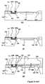
- a sensing device according to the inventionis shown in Figures 1 and 2 .
- the sensorhas a silicon part 10, formed on a substrate 100 with a rigid support rim 101, and a surface layer as part of the rim 101 of a first conduction type and a thin flexible diaphragm 103.
- the silicon substrate 10contains an electrical conduction system comprising doped conductors 106 of a second conduction type buried under an epitaxial layer 102 of a first conduction type and metal interconnects 108 and 109.
- the buried conductors 106 and the metal interconnects 108 and 109are electrically connected to each other via plug diffusions 105a and 105b of a second conduction type and through contact holes formed in a surface passivation layer 111.
- a recessis etched in the silicon part in an area extending across the diaphragm.
- a first glass part 120has a thin-film surface conduction system 121 on its surface formed by metal interconnects and forming a plate electrode facing the silicon diaphragm 103.
- the glass 120is anodically bonded to the silicon part 10 thereby forming a complete seal ring 130.
- the etched recess in the silicon partforms a scaled vacuum reference volume 115.
- the substrate 10 and the glass part 120form a capacitive sensing device with the metal layer 121, on the glass 120, acting as the first electrode.
- This electrodeis electrically connected to a wire bonding pad 109, that is outside of the sealed cavity, via a press contact formed between the electrode 121, the interconnect 108 and the buried conductor 106 under the sealed area 130.
- the sealed cavity 115acts as the electrical isolation gap in the capacitor.
- the flexible diaphragm 103is the second electrode of the variable capacitor, electrically connected via the surface layer 101 to a wire bond pad 112 outside the sealed cavity (not shown in Figure 1 ).
- the sensing functionis provided by an increase in capacitance when a pressure acts on the diaphragm 103 to press the diaphragm in the direction towards the counter electrode 121 on the glass, giving a smaller gap 115 in the capacitor.
- a second glass substrate 125is bonded to the silicon substrate with a seal 127.
- the bondingmay be performed, for example, by anodic bonding.
- the sensing devicemay modified as shown in Figure 4 with a centre boss structure 104 to stiffen the centre part of the silicon diaphragm.
- the sensing devicemay be modified as shown in Figure 5 with wire bond pads 129 on the glass 120 and additional press contacts 123 between interconnects on glass and the silicon part.
- a sensing device built as two capacitorsis shown in Figure 7 .
- one of the capacitorsis made, according to the description above, as a pressure sensitive capacitor and the other capacitor is identical except that it is not pressure sensitive as it does not have a pressure inlet. Consequently, no pressure difference is experienced over the diaphragm 233.
- the two capacitorsare otherwise identical in orderto achieve the best possible match of their capacitance values when no pressure is applied.
- the sensing devicecan be built as a differential pressure sensor, as shown in Figure 8 , with two inlets 326, 336 and a common vacuum reference volume 315, 335.
- Figure 9illustrates an exemplary sequence of a manufacturing process suitable for manufacturing a device according to the present invention (as illustrated in Figure 4 ). It can be seen that the simplicity of the sequence lends itself to an uncomplicated, and consequently low cost, manufacturing process.
- the processingstarts with a p-type silicon substrate 100 with ⁇ 1-0-0> orientation, (see Figure 9a ).
- Standard lithographic methods, ion implantation and high temperature diffusion of n-type doping such as Phosphorousis used to form n-regions 101 and 104 in the substrate, see Figure 9b .
- the next stepis forming p-type regions 106 by implantation and drive-in diffusion of boron.
- An n-type epitaxial layer 102is thereafter grown on top of the silicon substrate to form buried p-regions 106 (see Figure 9c ).
- Recessesare then etched on the surface 102 by dry etching and/or wet etching as shown in Figure 9d .
- the electrochemical etchingextends to the pn-junctions between the substrate 100 and the n-regions 101, 104 and the n-type epitaxial layer 102.
- a pressure sensitive diaphragmis now formed with thin flexible areas formed as part of the epitaxial layer 102 and with a stiff centre section 101b.
- Manufacture of this sensing deviceis completed by anodically bonding, in a vacuum, a glass substrate 120 with metal electrode and thin film interconnects 121 already formed thereon, to the silicon substrate 100, resulting in a structure as shown in Figures 9g and 4 , with the anodic bonded seal area 130 and the sealed cavity 115 formed by the recesses etched in the surface of the silicon substrate.
Landscapes
- Physics & Mathematics (AREA)
- General Physics & Mathematics (AREA)
- Electromagnetism (AREA)
- Measuring Fluid Pressure (AREA)
- Pressure Sensors (AREA)
Description
- Pressure sensors are extensively used in a large and increasingly varied field, including important areas such as medical instrumentation, automotive applications such as engine control and tyre pressure monitoring, industrial process control and the avionics industry. The most commonly used conversion principles for silicon based pressure sensors are capacitive detection and piezoresistive detection.
- Piezoresistive sensors are generally considered to be more robust than capacitive sensors. Another advantage is that they give an output signal proportional to the input with good linearity. Capacitive sensors, on the other hand, have the advantage over the piezoresistive type in that they consume less power, but have a non-linear direct output signal and are more sensitive to electromagnetic interference. Capacitive silicon sensors can be made to be small in size and can easily be made by surface micromachinirig. However, they are not very robust and their pressure sensitive diaphragm needs to be protected against the pressure media by a gel or other flexible material in most applications. This results in an increase in vibration sensitivity due to the mass added to the top of the diaphragm. Advanced and well proven methods of manufacturing silicon pressure sensors and inertial sensors are described in the patent publications
EP-A-742581 EP-A-994330 US4390925 discloses a method for manufacturing a variable capacitance pressure transducer having a plurality of recesses and interconnecting paths etched into the surface of a silicon wafer. A glass plate having thin-film metal deposits on the surface thereof is electrostatically bonded to the silicon.- The present invention seeks to provide a capacitive silicon sensor arrangement for the measurement of pressure that overcomes the above mentioned problems.
- According to the present invention there is provided a capacitive-type pressure sensor comprising:
- a glass substrate having an electrode formed thereon; and
- a diaphragm formed from a semiconductor material and bonded to said glass substrate to define an enclosed cavity containing at least a portion of said electrode, to thereby define a capacitive element, through which, in use, an electrical signal may be passed to determine a capacitance thereof which is indicative of the pressure to be determined,
- wherein an electrical connector is provided to each of said electrode and said diaphragm,
- characterised in that the electrical connector for said electrode is provided by buried doped conductors being formed beneath the surface of said semiconductor material, and by plug diffusions, both buried doped conductors and plug diffusions being of the same conduction type,
- the sensor further comprising press contacts, a first press contact being formed between said electrode and said buried conductor, and a second press contact being arranged to allow for interaction with devices interconnected with said sensor.
- The sensor has a pressure sensitive diaphragm acting as the movable electrode in the capacitor, an on-chip vacuum reference volume preferably sealed by anodic bonding acting as the gap in the capacitor and with the counter electrode of the capacitor on glass. These are connected to the outside of the sealed cavity by a conduction system consisting of metal interconnects on the glass, press contacts between the metal on glass and metal on the silicon part; and with buried conductors in the silicon substrate for crossing of the hermetically sealed cavity to metal interconnects and wire bonding areas outside the sealed area. The invention results in a robust and reliable pressure sensor with good media compatibility. The process technology that is used results in low manufacturing cost which is beneficial for high volume applications such as in the automotive industry.
- Higher measurement accuracy can be achieved by incorporating a second and matching capacitor on the same chip as the pressure sensitive capacitor and measuring the relative differences in the two capacitance values. The high accuracy is obtained by the good matching and tracking of the zero-point over temperature and time of the two capacitors values due to the near identical effects of packaging stress on the two capacitors.
- This invention is made possible by using silicon planar processing combined with modem silicon bulk micromachining processes such as dry etching, anisotropic and selective etching, thin-film metallization of glass and anodic bonding, all well known within microsystem technology (MST) and micro-electro-mechanical systems (MEMS).
- For a good understanding of the invention and its features and advantages, reference is made to the drawings, in which:
Figure 1 is a cross sectional view of a first type of a capacitive absolute pressure sensor in accordance with the present invention;Figure 2 is a top plan view of the pressure sensor ofFigure 1 , the cross sectional view ofFigure 1 being through the line A-A;Figure 3 is a cross-sectional view of the sensor ofFigure 1 , but with a second glass layer for improved mechanical stability and with a pressure inlet port through a first glass layer;Figure 4 shows the example ofFigure 3 with a bossed centre section for the diaphragm for a more piston type movement of the diaphragm when exposed to pressure;Figure 5 is a cross sectional view of a second type of a capacitive pressure sensor in accordance with the present invention and having electrical interconnections on its glass layer;Figure 6 shows a capacitive measurement bridge, that can be used in a high accuracy version of the invention, using two matched capacitors;Figure 7 is a cross-sectional view of a chip with two matched capacitors according to the invention, one of which has a pressure inlet and the other of which is sealed and used as a matched reference;Figure 8 is a differential measurement device according to the invention; andFigure 9 is a process sequence that can be used to form the sensor shown inFigure 4 .- A sensing device according to the invention is shown in
Figures 1 and2 . - The sensor has a
silicon part 10, formed on asubstrate 100 with arigid support rim 101, and a surface layer as part of therim 101 of a first conduction type and a thinflexible diaphragm 103. Thesilicon substrate 10 contains an electrical conduction system comprising dopedconductors 106 of a second conduction type buried under anepitaxial layer 102 of a first conduction type andmetal interconnects conductors 106 and themetal interconnects plug diffusions surface passivation layer 111. A recess is etched in the silicon part in an area extending across the diaphragm. - A
first glass part 120 has a thin-filmsurface conduction system 121 on its surface formed by metal interconnects and forming a plate electrode facing thesilicon diaphragm 103. Theglass 120 is anodically bonded to thesilicon part 10 thereby forming acomplete seal ring 130. The etched recess in the silicon part forms a scaledvacuum reference volume 115. - The
substrate 10 and theglass part 120 form a capacitive sensing device with themetal layer 121, on theglass 120, acting as the first electrode. This electrode is electrically connected to awire bonding pad 109, that is outside of the sealed cavity, via a press contact formed between theelectrode 121, theinterconnect 108 and the buriedconductor 106 under thesealed area 130. The sealedcavity 115 acts as the electrical isolation gap in the capacitor. Theflexible diaphragm 103 is the second electrode of the variable capacitor, electrically connected via thesurface layer 101 to awire bond pad 112 outside the sealed cavity (not shown inFigure 1 ). - The sensing function is provided by an increase in capacitance when a pressure acts on the
diaphragm 103 to press the diaphragm in the direction towards thecounter electrode 121 on the glass, giving asmaller gap 115 in the capacitor. - Preferably, as shown in
Figure 3 , asecond glass substrate 125, with ahole 126, is bonded to the silicon substrate with aseal 127. The bonding may be performed, for example, by anodic bonding. - The sensing device may modified as shown in
Figure 4 with acentre boss structure 104 to stiffen the centre part of the silicon diaphragm. - The sensing device may be modified as shown in
Figure 5 withwire bond pads 129 on theglass 120 andadditional press contacts 123 between interconnects on glass and the silicon part. - In the above examples pressure sensors with one capacitor have been shown. For applications that will require high total measurement accuracy, including low long term drift it is possible to adapt the above devices.
- A sensing device built as two capacitors is shown in
Figure 7 . In this device, one of the capacitors is made, according to the description above, as a pressure sensitive capacitor and the other capacitor is identical except that it is not pressure sensitive as it does not have a pressure inlet. Consequently, no pressure difference is experienced over thediaphragm 233. The two capacitors are otherwise identical in orderto achieve the best possible match of their capacitance values when no pressure is applied. - The sensing device can be built as a differential pressure sensor, as shown in
Figure 8 , with twoinlets vacuum reference volume Figure 9 illustrates an exemplary sequence of a manufacturing process suitable for manufacturing a device according to the present invention (as illustrated inFigure 4 ). It can be seen that the simplicity of the sequence lends itself to an uncomplicated, and consequently low cost, manufacturing process.- In this example, the processing starts with a p-
type silicon substrate 100 with <1-0-0> orientation, (seeFigure 9a ). Standard lithographic methods, ion implantation and high temperature diffusion of n-type doping such as Phosphorous is used to form n-regions Figure 9b . The next step is forming p-type regions 106 by implantation and drive-in diffusion of boron. An n-typeepitaxial layer 102 is thereafter grown on top of the silicon substrate to form buried p-regions 106 (seeFigure 9c ). Recesses are then etched on thesurface 102 by dry etching and/or wet etching as shown inFigure 9d . In this figure two etching steps have been performed, one to form the distance for thepress contacts 108 that will be formed later as shown inFigure 9e ; the other to form the gap in the capacitor (seeFigure 9g notation D).Contact diffusion regions conductor 106. Contact holes are then formed in apassivation layer 111 and followed by formation of metal interconnect andwire bonding areas 109, as shown inFigure 9e , using a metal such as aluminium. Anisotropic and selective etching, using an etch mask on the opposite side of the substrate is thereafter performed as shown inFigure 9f . The electrochemical etching extends to the pn-junctions between thesubstrate 100 and the n-regions type epitaxial layer 102. A pressure sensitive diaphragm is now formed with thin flexible areas formed as part of theepitaxial layer 102 and with a stiff centre section 101b. - Manufacture of this sensing device is completed by anodically bonding, in a vacuum, a
glass substrate 120 with metal electrode and thin film interconnects 121 already formed thereon, to thesilicon substrate 100, resulting in a structure as shown inFigures 9g and4 , with the anodic bondedseal area 130 and the sealedcavity 115 formed by the recesses etched in the surface of the silicon substrate.
Claims (13)
- A capacitive-type pressure sensor comprising:a glass substrate (120) having an electrode (121) formed thereon; anda diaphragm (103) formed from a semiconductor material and bonded to said glass substrate (120) to define an enclosed cavity (115) containing at least a portion of said electrode (121), to thereby define a capacitive element, through which, in use, an electrical signal may be passed to determine a capacitance thereof which is indicative of the pressure to be determined,wherein an electrical connector is provided to each of said electrode (121) and said diaphragm (103),characterised in that the electrical connector for said electrode (121) is provided by buried doped conductors (106) being formed beneath the surface of said semiconductor material, and by plug diffusions (105a, 105b), both buried doped conductors and plug diffusions being of the same conduction type,the sensor further comprising press contacts, a first press contact being formed between said electrode (121) and said buried conductor (106), and a second press contact being arranged to allow for interaction with devices interconnected with said sensor.
- A pressure sensor according to claim 1, wherein the diaphragm (103) is a micro-machined diaphragm formed by micro-machining the semiconductor material.
- A pressure sensor according to claim 1 or claim 2, wherein the semiconductor material is silicon.
- A pressure sensor according to any preceding claim, wherein the semiconductor material comprises a rigid support rim (101).
- A pressure sensor according to any preceding claim, wherein the electrical connector for the diaphragm (103) is provided by the semiconductor material.
- A pressure sensor according to any preceding claim, wherein the seal between the glass substrate (120) and the semiconductor material is provided by anodic bonding.
- A pressure sensor according to any preceding claim, wherein a second glass substrate (125) with a hole forming a pressure inlet port, in use, is bonded to the semiconductor material such that a layer of semiconductor material is sandwiched between two layers of glass substrate (120, 125).
- A pressure sensor according to any preceding claim, wherein the diaphragm (103) includes a stiff centre boss.
- A pressure sensor system comprising at least two capacitive-type pressure sensors according to any preceding claim.
- A pressure sensor system according to claim 9, wherein the diaphragm (103) of each of the pressure sensors, is formed from a single section of semiconductor material.
- A pressure sensor system according to claim 9 or claim 10, wherein each of the pressure sensors shares the same glass substrate (120).
- A pressure sensor system according to any of claims 9 to 11, wherein each pressure sensor is provided with a pressure inlet port, such that the system is a differential pressure sensor device.
- A pressure sensor system according to any of claims 9 to 11, wherein one pressure sensor is not provided with a pressure inlet port, such that this sensor is used as a reference sensor.
Priority Applications (6)
| Application Number | Priority Date | Filing Date | Title |
|---|---|---|---|
| EP02253102.4AEP1359402B1 (en) | 2002-05-01 | 2002-05-01 | Pressure sensor |
| US10/385,283US6874367B2 (en) | 2002-05-01 | 2003-03-10 | Pressure sensor |
| KR10-2003-0016133AKR20030086228A (en) | 2002-05-01 | 2003-03-14 | Pressure sensor |
| BR0300955-6ABR0300955A (en) | 2002-05-01 | 2003-04-11 | Capacitive type pressure sensor and pressure sensor system |
| CNB031243541ACN1279340C (en) | 2002-05-01 | 2003-04-30 | Pressure Sensor |
| JP2003124916AJP2004132947A (en) | 2002-05-01 | 2003-04-30 | Pressure sensor |
Applications Claiming Priority (1)
| Application Number | Priority Date | Filing Date | Title |
|---|---|---|---|
| EP02253102.4AEP1359402B1 (en) | 2002-05-01 | 2002-05-01 | Pressure sensor |
Publications (2)
| Publication Number | Publication Date |
|---|---|
| EP1359402A1 EP1359402A1 (en) | 2003-11-05 |
| EP1359402B1true EP1359402B1 (en) | 2014-10-01 |
Family
ID=28799736
Family Applications (1)
| Application Number | Title | Priority Date | Filing Date |
|---|---|---|---|
| EP02253102.4AExpired - LifetimeEP1359402B1 (en) | 2002-05-01 | 2002-05-01 | Pressure sensor |
Country Status (6)
| Country | Link |
|---|---|
| US (1) | US6874367B2 (en) |
| EP (1) | EP1359402B1 (en) |
| JP (1) | JP2004132947A (en) |
| KR (1) | KR20030086228A (en) |
| CN (1) | CN1279340C (en) |
| BR (1) | BR0300955A (en) |
Families Citing this family (64)
| Publication number | Priority date | Publication date | Assignee | Title |
|---|---|---|---|---|
| US7420659B1 (en) | 2000-06-02 | 2008-09-02 | Honeywell Interantional Inc. | Flow control system of a cartridge |
| US7111518B1 (en)* | 2003-09-19 | 2006-09-26 | Silicon Microstructures, Inc. | Extremely low cost pressure sensor realized using deep reactive ion etching |
| US7096738B2 (en)* | 2004-03-18 | 2006-08-29 | Rosemount Inc. | In-line annular seal-based pressure device |
| US7028552B2 (en)* | 2004-05-17 | 2006-04-18 | Kavlico Corporation | Reliable piezo-resistive pressure sensor |
| US6952955B1 (en) | 2004-07-28 | 2005-10-11 | Lear Corporation | Adjustable mounting of tire monitoring assembly |
| US6904795B1 (en) | 2004-09-14 | 2005-06-14 | Lear Corporation | Sealed mounting of tire monitoring assembly |
| US6923069B1 (en) | 2004-10-18 | 2005-08-02 | Honeywell International Inc. | Top side reference cavity for absolute pressure sensor |
| US7346178B2 (en)* | 2004-10-29 | 2008-03-18 | Silicon Matrix Pte. Ltd. | Backplateless silicon microphone |
| US7222639B2 (en) | 2004-12-29 | 2007-05-29 | Honeywell International Inc. | Electrostatically actuated gas valve |
| US7328882B2 (en) | 2005-01-06 | 2008-02-12 | Honeywell International Inc. | Microfluidic modulating valve |
| US7445017B2 (en) | 2005-01-28 | 2008-11-04 | Honeywell International Inc. | Mesovalve modulator |
| EP1707931B1 (en)* | 2005-03-31 | 2013-03-27 | STMicroelectronics Srl | Analog data-input device provided with a microelectromechanical pressure sensor |
| US7517201B2 (en) | 2005-07-14 | 2009-04-14 | Honeywell International Inc. | Asymmetric dual diaphragm pump |
| US7622782B2 (en) | 2005-08-24 | 2009-11-24 | General Electric Company | Pressure sensors and methods of making the same |
| EP1762925B1 (en)* | 2005-09-09 | 2016-12-21 | STMicroelectronics Srl | Analog input device with integrated pressure sensor and electronic apparatus equipped with said input device. |
| US7624755B2 (en) | 2005-12-09 | 2009-12-01 | Honeywell International Inc. | Gas valve with overtravel |
| EP1811666A1 (en)* | 2006-01-19 | 2007-07-25 | 3M Innovative Properties Company | Proximity sensor and method for manufacturing the same |
| US7523762B2 (en) | 2006-03-22 | 2009-04-28 | Honeywell International Inc. | Modulating gas valves and systems |
| US7487681B1 (en)* | 2006-08-06 | 2009-02-10 | Silicon Microstructures Inc. | Pressure sensor adjustment using backside mask |
| KR101004574B1 (en) | 2006-09-06 | 2010-12-30 | 히타치 긴조쿠 가부시키가이샤 | Semiconductor sensor device and manufacturing method thereof |
| US7543604B2 (en)* | 2006-09-11 | 2009-06-09 | Honeywell International Inc. | Control valve |
| US7644731B2 (en) | 2006-11-30 | 2010-01-12 | Honeywell International Inc. | Gas valve with resilient seat |
| CN101620022B (en)* | 2008-07-01 | 2011-12-21 | 欣兴电子股份有限公司 | Pressure sensing element package and manufacturing method thereof |
| US7793550B2 (en) | 2008-08-25 | 2010-09-14 | Infineon Technologies Ag | Sensor device including two sensors embedded in a mold material |
| US8358047B2 (en)* | 2008-09-29 | 2013-01-22 | Xerox Corporation | Buried traces for sealed electrostatic membrane actuators or sensors |
| US8072056B2 (en) | 2009-06-10 | 2011-12-06 | Medtronic, Inc. | Apparatus for restricting moisture ingress |
| US8172760B2 (en) | 2009-06-18 | 2012-05-08 | Medtronic, Inc. | Medical device encapsulated within bonded dies |
| US11169010B2 (en)* | 2009-07-27 | 2021-11-09 | Integra Lifesciences Switzerland Sàrl | Method for the calibration of an implantable sensor |
| CN101661012B (en)* | 2009-08-11 | 2013-03-13 | 南京理工大学 | Microfilm capacitive type surface stress sensor used for biochemical detection and manufacture method thereof |
| US8393222B2 (en)* | 2010-02-27 | 2013-03-12 | Codman Neuro Sciences Sárl | Apparatus and method for minimizing drift of a piezo-resistive pressure sensor due to progressive release of mechanical stress over time |
| US8490495B2 (en)* | 2010-05-05 | 2013-07-23 | Consensic, Inc. | Capacitive pressure sensor with vertical electrical feedthroughs and method to make the same |
| DE102010038534A1 (en)* | 2010-07-28 | 2012-02-02 | Robert Bosch Gmbh | Sensor element for capacitive differential pressure measurement |
| US8666505B2 (en) | 2010-10-26 | 2014-03-04 | Medtronic, Inc. | Wafer-scale package including power source |
| US8424388B2 (en) | 2011-01-28 | 2013-04-23 | Medtronic, Inc. | Implantable capacitive pressure sensor apparatus and methods regarding same |
| US8590387B2 (en) | 2011-03-31 | 2013-11-26 | DePuy Synthes Products, LLC | Absolute capacitive micro pressure sensor |
| DE102011081887A1 (en)* | 2011-08-31 | 2013-02-28 | Robert Bosch Gmbh | Polymer layer system pressure sensor device and polymer layer system pressure sensor method |
| US8899264B2 (en) | 2011-12-15 | 2014-12-02 | Honeywell International Inc. | Gas valve with electronic proof of closure system |
| US8905063B2 (en) | 2011-12-15 | 2014-12-09 | Honeywell International Inc. | Gas valve with fuel rate monitor |
| US9851103B2 (en) | 2011-12-15 | 2017-12-26 | Honeywell International Inc. | Gas valve with overpressure diagnostics |
| US8947242B2 (en) | 2011-12-15 | 2015-02-03 | Honeywell International Inc. | Gas valve with valve leakage test |
| US9557059B2 (en) | 2011-12-15 | 2017-01-31 | Honeywell International Inc | Gas valve with communication link |
| US9995486B2 (en) | 2011-12-15 | 2018-06-12 | Honeywell International Inc. | Gas valve with high/low gas pressure detection |
| US9846440B2 (en) | 2011-12-15 | 2017-12-19 | Honeywell International Inc. | Valve controller configured to estimate fuel comsumption |
| US9835265B2 (en) | 2011-12-15 | 2017-12-05 | Honeywell International Inc. | Valve with actuator diagnostics |
| US8839815B2 (en) | 2011-12-15 | 2014-09-23 | Honeywell International Inc. | Gas valve with electronic cycle counter |
| US9074770B2 (en) | 2011-12-15 | 2015-07-07 | Honeywell International Inc. | Gas valve with electronic valve proving system |
| US9219020B2 (en) | 2012-03-08 | 2015-12-22 | Infineon Technologies Ag | Semiconductor device, wafer assembly and methods of manufacturing wafer assemblies and semiconductor devices |
| US9234661B2 (en) | 2012-09-15 | 2016-01-12 | Honeywell International Inc. | Burner control system |
| US10422531B2 (en) | 2012-09-15 | 2019-09-24 | Honeywell International Inc. | System and approach for controlling a combustion chamber |
| US9366593B2 (en)* | 2013-09-27 | 2016-06-14 | Infineon Technologies Ag | Pressure sensor package with integrated sealing |
| EP2868970B1 (en) | 2013-10-29 | 2020-04-22 | Honeywell Technologies Sarl | Regulating device |
| CN103606565B (en)* | 2013-11-27 | 2016-05-11 | 苏州科技学院 | The manufacturing process of pressure sensor sensing element |
| US10024439B2 (en) | 2013-12-16 | 2018-07-17 | Honeywell International Inc. | Valve over-travel mechanism |
| US9267857B2 (en)* | 2014-01-07 | 2016-02-23 | Honeywell International Inc. | Pressure sensor having a bossed diaphragm |
| JP6331447B2 (en)* | 2014-02-14 | 2018-05-30 | オムロン株式会社 | Capacitance type pressure sensor and input device |
| US9841122B2 (en) | 2014-09-09 | 2017-12-12 | Honeywell International Inc. | Gas valve with electronic valve proving system |
| US9645584B2 (en) | 2014-09-17 | 2017-05-09 | Honeywell International Inc. | Gas valve with electronic health monitoring |
| US10503181B2 (en) | 2016-01-13 | 2019-12-10 | Honeywell International Inc. | Pressure regulator |
| US10549982B2 (en) | 2016-02-15 | 2020-02-04 | Stmicroelectronics S.R.L. | Pressure sensor encapsulated in elastomeric material, and system including the pressure sensor |
| US10221062B2 (en)* | 2016-10-03 | 2019-03-05 | Continental Automotive Systems, Inc. | Cavity with silicon on insulator MEMS pressure sensing device with an extended shallow cross-shaped cavity |
| US10564062B2 (en) | 2016-10-19 | 2020-02-18 | Honeywell International Inc. | Human-machine interface for gas valve |
| CN107290084B (en)* | 2017-06-28 | 2019-08-30 | 京东方科技集团股份有限公司 | A kind of pressure sensor and its manufacturing method, electronic device |
| US11073281B2 (en) | 2017-12-29 | 2021-07-27 | Honeywell International Inc. | Closed-loop programming and control of a combustion appliance |
| US10697815B2 (en) | 2018-06-09 | 2020-06-30 | Honeywell International Inc. | System and methods for mitigating condensation in a sensor module |
Citations (1)
| Publication number | Priority date | Publication date | Assignee | Title |
|---|---|---|---|---|
| WO1996013705A1 (en)* | 1994-10-29 | 1996-05-09 | Joshua Lanter | Process for producing lead-throughs for electric lines through gastight connections between glass and silicon or the like and gastight lead-throughs in such connections and pressure sensors comprising such lead-throughs |
Family Cites Families (20)
| Publication number | Priority date | Publication date | Assignee | Title |
|---|---|---|---|---|
| US4426673A (en)* | 1976-03-12 | 1984-01-17 | Kavlico Corporation | Capacitive pressure transducer and method of making same |
| US4388668A (en)* | 1976-03-12 | 1983-06-14 | Kaylico Corporation | Capacitive pressure transducer |
| US4390925A (en)* | 1981-08-26 | 1983-06-28 | Leeds & Northrup Company | Multiple-cavity variable capacitance pressure transducer |
| FI75426C (en)* | 1984-10-11 | 1988-06-09 | Vaisala Oy | ABSOLUTTRYCKGIVARE. |
| US4730496A (en)* | 1986-06-23 | 1988-03-15 | Rosemount Inc. | Capacitance pressure sensor |
| US4872945A (en)* | 1986-06-25 | 1989-10-10 | Motorola Inc. | Post seal etching of transducer diaphragm |
| US5113868A (en)* | 1987-06-01 | 1992-05-19 | The Regents Of The University Of Michigan | Ultraminiature pressure sensor with addressable read-out circuit |
| US4996627A (en)* | 1989-01-30 | 1991-02-26 | Dresser Industries, Inc. | High sensitivity miniature pressure transducer |
| US5174156A (en)* | 1990-07-27 | 1992-12-29 | Honeywell Inc. | Pressure transducer with reduced offset signal |
| DE4207952C1 (en)* | 1992-03-10 | 1993-04-15 | Mannesmann Ag, 4000 Duesseldorf, De | Capacitative differential pressure sensor for simple mfr. - comprises silicon diaphragm with edges having thinned areas, leaving central area, pressure input channels aligned with thickened edge region, and flat recesses |
| JPH0666658A (en)* | 1992-08-15 | 1994-03-11 | Stec Kk | Capacitive pressure sensor |
| JPH07167725A (en)* | 1993-12-14 | 1995-07-04 | Yazaki Corp | Capacitive pressure sensor and manufacturing method thereof |
| FI100918B (en)* | 1995-02-17 | 1998-03-13 | Vaisala Oy | Surface micromechanical, symmetrical pressure differential sensor |
| JP3107516B2 (en)* | 1996-05-01 | 2000-11-13 | 株式会社日立製作所 | Composite sensor |
| US5792958A (en)* | 1997-01-21 | 1998-08-11 | Honeywell Inc. | Pressure sensor with a compressible insert to prevent damage from freezing |
| JP3299715B2 (en)* | 1998-04-01 | 2002-07-08 | 長野計器株式会社 | Chip potential extraction structure and manufacturing method |
| US6109113A (en)* | 1998-06-11 | 2000-08-29 | Delco Electronics Corp. | Silicon micromachined capacitive pressure sensor and method of manufacture |
| WO2000011444A1 (en)* | 1998-08-19 | 2000-03-02 | Wisconsin Alumni Research Foundation | Sealed capacitive pressure sensors |
| KR100300527B1 (en)* | 1998-09-03 | 2001-10-27 | 윤덕용 | Remote pressure monitoring device of sealed type and manufacture method for the same |
| DE19931773C1 (en)* | 1999-07-08 | 2000-11-30 | Daimler Chrysler Ag | Micromechanical component has contact ducts formed as metal wires which are recast from the molten glass during the manufacture of the first wafer |
- 2002
- 2002-05-01EPEP02253102.4Apatent/EP1359402B1/ennot_activeExpired - Lifetime
- 2003
- 2003-03-10USUS10/385,283patent/US6874367B2/ennot_activeExpired - Lifetime
- 2003-03-14KRKR10-2003-0016133Apatent/KR20030086228A/ennot_activeWithdrawn
- 2003-04-11BRBR0300955-6Apatent/BR0300955A/ennot_activeApplication Discontinuation
- 2003-04-30CNCNB031243541Apatent/CN1279340C/ennot_activeExpired - Fee Related
- 2003-04-30JPJP2003124916Apatent/JP2004132947A/enactivePending
Patent Citations (1)
| Publication number | Priority date | Publication date | Assignee | Title |
|---|---|---|---|---|
| WO1996013705A1 (en)* | 1994-10-29 | 1996-05-09 | Joshua Lanter | Process for producing lead-throughs for electric lines through gastight connections between glass and silicon or the like and gastight lead-throughs in such connections and pressure sensors comprising such lead-throughs |
Also Published As
| Publication number | Publication date |
|---|---|
| EP1359402A1 (en) | 2003-11-05 |
| US6874367B2 (en) | 2005-04-05 |
| CN1455234A (en) | 2003-11-12 |
| KR20030086228A (en) | 2003-11-07 |
| CN1279340C (en) | 2006-10-11 |
| JP2004132947A (en) | 2004-04-30 |
| BR0300955A (en) | 2004-08-10 |
| US20030205090A1 (en) | 2003-11-06 |
Similar Documents
| Publication | Publication Date | Title |
|---|---|---|
| EP1359402B1 (en) | Pressure sensor | |
| US7150195B2 (en) | Sealed capacitive sensor for physical measurements | |
| EP0720731B1 (en) | Suspended diaphragm pressure sensor | |
| US7918136B2 (en) | Micromechanical sensor element | |
| JP5568803B2 (en) | High temperature medium compatible electrical insulation pressure sensor | |
| EP1953516B1 (en) | Micromechanical pressure sensing device | |
| US7998777B1 (en) | Method for fabricating a sensor | |
| CN106092428B (en) | Pressure sensor device with high sensitivity and high accuracy | |
| US4852408A (en) | Stop for integrated circuit diaphragm | |
| CN107894294B (en) | Silicon-on-insulator MEMS pressure sensing device with cavity and extended shallow polygonal cavity | |
| CN213812675U (en) | High-temperature pressure sensor chip for realizing leadless package | |
| EP0672898B1 (en) | Semiconductor pressure sensor with polysilicon diaphragm and single-crystal gage elements and fabrication method therefor | |
| CN113428829B (en) | MEMS (micro-electromechanical system) wet-pressing integrated sensor and preparation method thereof | |
| KR20010032103A (en) | Micromechanical differential pressure sensor device | |
| US5932809A (en) | Sensor with silicon strain gage | |
| US20240302236A1 (en) | Sensor Package With A Sensor Die | |
| CN114184309B (en) | Piezoresistive MEMS sensor and preparation method thereof | |
| CN113353883B (en) | MEMS pressure sensor based on phase detection principle and preparation method | |
| WO2001000523A9 (en) | Micro-electromechanical devices and methods of manufacture | |
| Subramanian et al. | Scalable vertical diaphragm pressure sensors: Device and process design, design for packaging | |
| CN115615587B (en) | Pressure sensor | |
| Yang et al. | The SOI-like method to reduce the die size of bulk-micromachined sensors |
Legal Events
| Date | Code | Title | Description |
|---|---|---|---|
| PUAI | Public reference made under article 153(3) epc to a published international application that has entered the european phase | Free format text:ORIGINAL CODE: 0009012 | |
| AK | Designated contracting states | Kind code of ref document:A1 Designated state(s):AT BE CH CY DE DK ES FI FR GB GR IE IT LI LU MC NL PT SE TR | |
| AX | Request for extension of the european patent | Extension state:AL LT LV MK RO SI | |
| 17P | Request for examination filed | Effective date:20040419 | |
| AKX | Designation fees paid | Designated state(s):DE FR GB | |
| RAP1 | Party data changed (applicant data changed or rights of an application transferred) | Owner name:INFINEON TECHNOLOGIES SENSONOR AS | |
| 17Q | First examination report despatched | Effective date:20061103 | |
| RAP1 | Party data changed (applicant data changed or rights of an application transferred) | Owner name:INFINEON TECHNOLOGIES AG | |
| GRAP | Despatch of communication of intention to grant a patent | Free format text:ORIGINAL CODE: EPIDOSNIGR1 | |
| INTG | Intention to grant announced | Effective date:20140417 | |
| GRAS | Grant fee paid | Free format text:ORIGINAL CODE: EPIDOSNIGR3 | |
| GRAA | (expected) grant | Free format text:ORIGINAL CODE: 0009210 | |
| AK | Designated contracting states | Kind code of ref document:B1 Designated state(s):DE FR GB | |
| REG | Reference to a national code | Ref country code:GB Ref legal event code:FG4D | |
| REG | Reference to a national code | Ref country code:DE Ref legal event code:R096 Ref document number:60246667 Country of ref document:DE Effective date:20141113 | |
| REG | Reference to a national code | Ref country code:DE Ref legal event code:R097 Ref document number:60246667 Country of ref document:DE | |
| PLBE | No opposition filed within time limit | Free format text:ORIGINAL CODE: 0009261 | |
| STAA | Information on the status of an ep patent application or granted ep patent | Free format text:STATUS: NO OPPOSITION FILED WITHIN TIME LIMIT | |
| 26N | No opposition filed | Effective date:20150702 | |
| GBPC | Gb: european patent ceased through non-payment of renewal fee | Effective date:20150501 | |
| REG | Reference to a national code | Ref country code:FR Ref legal event code:ST Effective date:20160129 | |
| PG25 | Lapsed in a contracting state [announced via postgrant information from national office to epo] | Ref country code:GB Free format text:LAPSE BECAUSE OF NON-PAYMENT OF DUE FEES Effective date:20150501 | |
| PG25 | Lapsed in a contracting state [announced via postgrant information from national office to epo] | Ref country code:FR Free format text:LAPSE BECAUSE OF NON-PAYMENT OF DUE FEES Effective date:20150601 | |
| PGFP | Annual fee paid to national office [announced via postgrant information from national office to epo] | Ref country code:DE Payment date:20170718 Year of fee payment:16 | |
| REG | Reference to a national code | Ref country code:DE Ref legal event code:R119 Ref document number:60246667 Country of ref document:DE | |
| PG25 | Lapsed in a contracting state [announced via postgrant information from national office to epo] | Ref country code:DE Free format text:LAPSE BECAUSE OF NON-PAYMENT OF DUE FEES Effective date:20181201 |