EP1347515A1 - Chip differentiation on the reticule level - Google Patents
Chip differentiation on the reticule levelDownload PDFInfo
- Publication number
- EP1347515A1 EP1347515A1EP03354027AEP03354027AEP1347515A1EP 1347515 A1EP1347515 A1EP 1347515A1EP 03354027 AEP03354027 AEP 03354027AEP 03354027 AEP03354027 AEP 03354027AEP 1347515 A1EP1347515 A1EP 1347515A1
- Authority
- EP
- European Patent Office
- Prior art keywords
- circuit
- reticle
- transistor
- cell
- storage element
- Prior art date
- Legal status (The legal status is an assumption and is not a legal conclusion. Google has not performed a legal analysis and makes no representation as to the accuracy of the status listed.)
- Withdrawn
Links
- 230000004069differentiationEffects0.000titledescription6
- 238000002513implantationMethods0.000claimsabstractdescription18
- 238000003860storageMethods0.000claimsabstractdescription16
- 238000000034methodMethods0.000claimsabstractdescription14
- 239000002019doping agentSubstances0.000claimsabstractdescription12
- 230000006870functionEffects0.000claimsabstractdescription6
- 210000004027cellAnatomy0.000description37
- 230000015654memoryEffects0.000description25
- CIWBSHSKHKDKBQ-JLAZNSOCSA-NAscorbic acidChemical compoundOC[C@H](O)[C@H]1OC(=O)C(O)=C1OCIWBSHSKHKDKBQ-JLAZNSOCSA-N0.000description12
- 239000004065semiconductorSubstances0.000description8
- 238000004519manufacturing processMethods0.000description7
- 230000004048modificationEffects0.000description6
- 238000012986modificationMethods0.000description6
- 239000011347resinSubstances0.000description6
- 229920005989resinPolymers0.000description6
- 230000008901benefitEffects0.000description3
- XUIMIQQOPSSXEZ-UHFFFAOYSA-NSiliconChemical compound[Si]XUIMIQQOPSSXEZ-UHFFFAOYSA-N0.000description2
- 230000015572biosynthetic processEffects0.000description2
- 230000000295complement effectEffects0.000description2
- 238000010586diagramMethods0.000description2
- 238000005286illuminationMethods0.000description2
- 239000011159matrix materialSubstances0.000description2
- 230000003287optical effectEffects0.000description2
- 229910052710siliconInorganic materials0.000description2
- 239000010703siliconSubstances0.000description2
- 210000003771C cellAnatomy0.000description1
- 230000006399behaviorEffects0.000description1
- 230000008859changeEffects0.000description1
- 238000000151depositionMethods0.000description1
- 238000001514detection methodMethods0.000description1
- 230000008034disappearanceEffects0.000description1
- 239000007943implantSubstances0.000description1
- 238000009434installationMethods0.000description1
- 238000009413insulationMethods0.000description1
- 230000000873masking effectEffects0.000description1
- 238000001465metallisationMethods0.000description1
- 230000037361pathwayEffects0.000description1
- 230000005855radiationEffects0.000description1
Images

Classifications
- H—ELECTRICITY
- H01—ELECTRIC ELEMENTS
- H01L—SEMICONDUCTOR DEVICES NOT COVERED BY CLASS H10
- H01L23/00—Details of semiconductor or other solid state devices
- H01L23/57—Protection from inspection, reverse engineering or tampering
- H—ELECTRICITY
- H01—ELECTRIC ELEMENTS
- H01L—SEMICONDUCTOR DEVICES NOT COVERED BY CLASS H10
- H01L23/00—Details of semiconductor or other solid state devices
- H01L23/544—Marks applied to semiconductor devices or parts, e.g. registration marks, alignment structures, wafer maps
- H—ELECTRICITY
- H10—SEMICONDUCTOR DEVICES; ELECTRIC SOLID-STATE DEVICES NOT OTHERWISE PROVIDED FOR
- H10B—ELECTRONIC MEMORY DEVICES
- H10B20/00—Read-only memory [ROM] devices
- H—ELECTRICITY
- H10—SEMICONDUCTOR DEVICES; ELECTRIC SOLID-STATE DEVICES NOT OTHERWISE PROVIDED FOR
- H10D—INORGANIC ELECTRIC SEMICONDUCTOR DEVICES
- H10D89/00—Aspects of integrated devices not covered by groups H10D84/00 - H10D88/00
- H—ELECTRICITY
- H01—ELECTRIC ELEMENTS
- H01L—SEMICONDUCTOR DEVICES NOT COVERED BY CLASS H10
- H01L2223/00—Details relating to semiconductor or other solid state devices covered by the group H01L23/00
- H01L2223/544—Marks applied to semiconductor devices or parts
- H01L2223/54433—Marks applied to semiconductor devices or parts containing identification or tracking information
- H01L2223/5444—Marks applied to semiconductor devices or parts containing identification or tracking information for electrical read out
- H—ELECTRICITY
- H01—ELECTRIC ELEMENTS
- H01L—SEMICONDUCTOR DEVICES NOT COVERED BY CLASS H10
- H01L2223/00—Details relating to semiconductor or other solid state devices covered by the group H01L23/00
- H01L2223/544—Marks applied to semiconductor devices or parts
- H01L2223/54473—Marks applied to semiconductor devices or parts for use after dicing
- H—ELECTRICITY
- H01—ELECTRIC ELEMENTS
- H01L—SEMICONDUCTOR DEVICES NOT COVERED BY CLASS H10
- H01L2924/00—Indexing scheme for arrangements or methods for connecting or disconnecting semiconductor or solid-state bodies as covered by H01L24/00
- H01L2924/0001—Technical content checked by a classifier
- H01L2924/0002—Not covered by any one of groups H01L24/00, H01L24/00 and H01L2224/00
Definitions
- the present inventionrelates to the differentiation of integrated circuit chips produced in a single wafer semiconductor (wafer).
- circuitsTo manufacture integrated circuits, one realizes, in a semiconductor wafer, very many separate sets or integrated circuit chips. From one chip to another, the circuits can be functionally identical (homogeneous) or perform different (heterogeneous) functions.
- the present inventionaims to provide a method of differentiation of functionally identical integrated circuits and produced in the same semiconductor wafer which overcomes the disadvantages of known methods.
- the present inventionrelates more particularly to allow the storage of a binary code in manufacturing, without this code can be detected by optical observation of the chip.
- this inventionprovides a method of differentiating circuits integrated reproducing identical functions by storing a binary code in a planned non-volatile storage element in each circuit, the method consisting in providing, for each circuit of the same reticle, at least one layout selective of dopants from its memory element which is different from the selective implantation of the dopants of the elements memorizing other circuits.
- a single selective dopant implantationis modified from one circuit to another in the same reticle.
- the reticleis formed by incorporating at least one geometry defining the memorizing elements which is different from one circuit to another on the same reticle.
- the storage elementconsists of elementary cells which each include at least one MOS transistor.
- elementary cells of the storage elementinclude resistors.
- a feature of the present inventionis memorize a binary code, differentiating chips from integrated circuits performing the same function, by modifying a implantation of definition of specific regions of cells elementary memory (read only) containing the coded.
- cells elementary ROM memoriesinclude at least one transistor MOS type. Drain and source regions of the transistor are defined in the semiconductor wafer, by implantation selective of appropriate dopants.
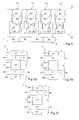
- Figure 1illustrates, in partial top view and schematic, a semiconductor wafer 1, during a step manufacturing intermediary of integrated circuits.
- an implantation maskintended to define, in slice 1, at least specific regions of cells elementary ROM memories in which are stored circuit identification codes.
- the masking operationconsists of depositing a photosensitive resin over the entire edge then subject specific regions of the resin to UV illumination. Depending on the type of resin (positive or negative), the lit - exposed - parts of the resin or no are then selectively eliminated so as to discover partially the semiconductor, for example silicon, constituting section 1.
- the design of the resinforms, circuit level, an installation mask reproducing the drawing interposed, during sunshine, between the light source and section 1. Thereafter, and unless otherwise specified, we will denote by mask, the optically interposed element, named also reticle.
- the exposureis carried out by means of a device having an illumination window W of dimensions lower than those in section 1.
- a reticlecomprising parts opaque to the radiation from the window and transparent parts to this one.
- section 1is moved so that its entire surface passes at a time given under the lighting window.
- the sliceis homogeneous, that is, the same reticle is used to expose the whole brochure.
- Figure 2shows a detail of Figure 1, know a reticle 2 (mask) of exposure of window W.
- the reticle 2will have dimensions such that several integrated circuit chips will be exposed simultaneously.
- the reticleis homogeneous, that is to say that the chips include each the same circuit.
- reticle 2corresponds to eight rows and eight columns, or 64 chips.
- a reticlecan include several hundred integrated circuits.
- FIG 3shows a detail of the reticle of the Figure 2, namely, one of the integrated circuits 3 which it defines.
- Each chip 3 according to the inventioncomprises a ROM memory 4 intended to store a binary code of identification of the circuit in progress.
- the memory 4consists of a matrix of elementary cells preferably of a single line or column.
- FIG. 4represents, partially and schematically, the equivalent electrical diagram of an embodiment possible from a memory for storing a binary code according to the invention.
- Figure 4represents only four cells C1, C2, C3 and C4.
- the number of memory cellsis preferably chosen depending on the number of circuits contained in the reticle so generate, with the bits of the memory, as many codes distinct that there are circuits on the reticle.
- the elementary cell Ccan be of any known type comprising at least one MOS transistor.
- cell Cis a pair differential of two transistors N1 and N2 connected in parallel between two supply lines L1 and L2, being each in series with a resistor R1, R2.
- R1 resistors and R2are obtained by selective implantation of dopants in silicon (polycrystalline or not).
- transistors N1 and N2are, for example, N channel.
- the gate of a given transistor N1, N2is connected to the drain of the other transistor N2, N1, respectively.
- the drain of transistor N1, common to the gate of the transistor N2,constitutes a reading terminal of the stored binary data B in cell C.
- the state of output of cell Cdepends on transistor N1 or N2 which becomes driver first after applying a positive front supply on line L1.
- the imbalance between the two transistors of each cell Ccomes from programming specific to the invention which will be explained later in relation with Figures 5A, 5B and 5C.
- the cellsare read in parallel.
- the exploitation of a memory according to the invention once programmeduses techniques reading classics according to the type of memory cells (one or several transistors) and their arrangement.
- the respective outputs of the cellsare linked to the entries of a register R of temporary storage of code when reading.
- the register Ris preferably reset after each reading so as not to leave the code, outside of periods when the application needs it. This will in the direction of increased security of the code. In any condition cause, register R is emptied when the circuit goes out by disappearance of the power supply (not shown).
- each memory cellcomprises, between lines L1 and L2, a single MOS transistor and, if applicable, a resistor. Reading is then carried out in series, using a comparator with a reference, the transistor serving as a selection element (and programming in the absence of resistance).
- An advantage of the embodiment of Figure 4is than a simple change of state of a signal applied to the line L1 (or L2) causes both the power and the reading of the code stored in memory.
- the programming of a cellis obtained by modifying the extent of implantation of definition of the source and drain regions of its transistors N1 and N2.
- FIG. 5Aillustrates an embodiment of a cell C in Figure 4 not programmed.
- the two N1 transistors and N2are carried out side by side in the same active area 5 of section 1.
- individual drain / source regions D1 and D2are located simultaneously, respectively at the top and at the bottom of Figure 5A.
- a common region S source / drain S1, S2 of transistors N1 and N2is installed, in the center of Figure 5A.
- tranche 1 and therefore the active area 5is doped with a first type of conductivity, for example P.
- the dopants implanted to define the regions of drain D1 and D2 and from source Sare of the conductivity type complementary, for example N.
- each transistor N1 and N2grids G1 and G2.
- the areas of drain regions D1 and D2 and source Sare as each grid G1 and G2 defines, in the active area 5, a channel region 6, 7 separating the common source S from a individual drain region D1, D2, respectively.
- programmingis carried out in modifying the extent of establishment, for example, of regions of source and drain of only one of transistors N1 and N2 of each cell.
- FIG. 5Billustrates a programming mode, in a cell C in FIG. 4, of a datum B in a first binary state considered here as "0".
- Figure 5Bdiffers from the Figure 5A in that the extent of one of the individual regions of drain / source of one of the transistors, for example the region D1 of transistor N1, is modified.
- the region modified D1is extended so that it reaches and merges with the common source region S. So, the G1 grid of transistor N1 crosses active region 5 vertically from continuous region D1-S.
- the gate G2 of the other transistor N2always defines a channel 7 in the active area 5 of type P.
- read accessi.e.
- the transistor N1then becomes more quickly conductive than the transistor N2. Indeed, it behaves like a resistance simple and it does not need a channel (6 in figures 5A and 5C) is created, unlike transistor N2.
- the transistor N1then replicates virtually on its output, i.e. its drain D1, a low reference level present on line L2.
- the gate G2 of the transistor N2being connected to this output, the recopy tends to block it in an open state that locks, at level of its drain D2, the high level of the positive front present on line L1.
- the drain D2being connected to the gate G1, the conduction imbalance is locked and cell C provides the register R with stable data in a first state binary considered, by convention, as "0".
- FIG. 5Cillustrates a programming mode in a cell C in FIG. 4 of a datum B in a second state binary considered here as "1".
- Figure 5Cdiffers from the FIG. 5A in that, compared with FIG. 5B, the extent of the other D2 of the individual drain / source regions of the other N2 of the transistors of cell C is extended so that it reaches and merges with the common source region S. So, channel 6 of transistor N1 is held in place then that channel 7 of transistor N2 is deleted and replaced by a D2-S region continues highly conductive. When accessing in reading, the behaviors of transistors N1 and N2 are then reversed. We therefore lock the drain D1 of transistor N1, that is to say the output of cell C, in a state complementary to the previous one considered here as "1".
- an elementary master drawing corresponding to a standard cell as described above in relation with Figure 5AThis master drawing is reproduced as many times as necessary inside the reticle 2 ( Figure 2) so that allow a simultaneous definition of the regions to be established all the chips 3 ( Figures 2 and 3) that it is necessary to ability to identify using binary code. Then inside the reticle 2, the extent of the various specific regions drain and / or source is changed from cell to cell the other inside the same chip and from one chip to another of separately, so as to memorize a code in each chip different.
- the formation of a maskis obtained by combination layers of drawings from a graphic database defining the circuit.
- the implantation mask on which acts the inventionis formed by incorporating, into the layers of drawings defining this mask, a geometry defining the zones of memory cells to be programmed.
- the inventioninstead of reproducing the same circuit all over the reticle (mask), we modify, from circuit to circuit, the geometry defining the implantations of the cells. We then obtains as many different circuits as positions on the reticle.
- the inventiondoes not in practice add any level of mask, and requires only a programming modification of a existing level.
- the reticleOnce the reticle has been made, it is interposed between the exposure window and the semiconductor wafer 1 of the way described above and the whole slice 1 is exposed step by step.
- the programming according to the inventionconsists in unbalancing the access resistors to the transistors of the programmed cells.
- each transistor N1, N2 of each cell Ccan be associated with a respective resistance R1, R2.
- Storing a binary code of differentiationcan be made according to the present invention by modifying an implantation mask for these resistors R1, R2.
- the gates G1, G2 of the transistorsare doped simultaneously with so as to increase their conductivity.
Landscapes
- Physics & Mathematics (AREA)
- Condensed Matter Physics & Semiconductors (AREA)
- General Physics & Mathematics (AREA)
- Engineering & Computer Science (AREA)
- Computer Hardware Design (AREA)
- Microelectronics & Electronic Packaging (AREA)
- Power Engineering (AREA)
- Semiconductor Memories (AREA)
Abstract
Translated fromFrenchDescription
Translated fromFrenchLa présente invention concerne la différenciation depuces de circuits intégrés réalisées dans une même tranchesemiconductrice (wafer).The present invention relates to the differentiation ofintegrated circuit chips produced in a single wafersemiconductor (wafer).
Pour fabriquer des circuits intégrés, on réalise, dansune tranche semiconductrice, de très nombreux ensembles distinctsou puces de circuits intégrés. D'une puce à une autre, lescircuits peuvent être fonctionnellement identiques (homogènes)ou réaliser des fonctions différentes (hétérogènes).To manufacture integrated circuits, one realizes, ina semiconductor wafer, very many separate setsor integrated circuit chips. From one chip to another, thecircuits can be functionally identical (homogeneous)or perform different (heterogeneous) functions.
Il peut être souhaitable de différencier des circuitsréalisant une même fonction (homogènes). Pour ce faire, on utilisegénéralement un identifiant de puce ou quantité secrète sous laforme d'un code binaire mémorisé dans une mémoire non volatile.Pour rendre cette mémoire inaccessible à un utilisateur, on doitfiger le code à la fabrication. On utilise alors une mémoire àlecture seulement, formée dans la même puce que le circuit ainsiidentifié. Les cellules mémoire correspondantes comportent aumoins un transistor de type MOS. Lors de la conception ducircuit, on supprime la grille de certains transistors decellules mémoire pour figer l'état (passant ou bloqué) de cestransistors et programmer ainsi les cellules mémoire concernées.Un inconvénient est que cela modifie alors l'aspect physique dela puce (on peut détecter optiquement la présence ou l'absence des grilles sur les zones d'isolant de champ qui séparent leszones actives des transistors). Le code mémorisé peut alors êtrereconstruit à partir de cette détection. Or, lorsque l'onsouhaite pourvoir une puce d'un identifiant en fabrication,c'est souvent que l'on souhaite préserver le secret de cetidentifiant.It may be desirable to differentiate circuitsperforming the same function (homogeneous). To do this, we useusually a chip or secret quantity identifier under theform of a binary code stored in a non-volatile memory.To make this memory inaccessible to a user, we mustfreeze the manufacturing code. We then use a memory atread only, formed in the same chip as the circuit as wellidentified. The corresponding memory cells includeminus one MOS type transistor. When designing thecircuit, we remove the grid of some transistors ofmemory cells to freeze the state (passing or blocked) of thesetransistors and thus program the memory cells concerned.One drawback is that it changes the physical appearance ofthe chip (we can optically detect the presence or absencegrids on the areas of field insulation that separate theactive areas of the transistors). The stored code can then bereconstructed from this detection. When wewishes to provide a chip with a manufacturing identifier,we often want to keep the secret of thisID.
La présente invention vise à proposer un procédé dedifférenciation de circuits intégrés fonctionnellement identiqueset réalisés dans une même tranche semiconductrice qui pallie lesinconvénients des procédés connus.The present invention aims to provide a method ofdifferentiation of functionally identical integrated circuitsand produced in the same semiconductor wafer which overcomes thedisadvantages of known methods.
La présente invention vise plus particulièrement àpermettre le stockage d'un code binaire en fabrication, sans quece code soit détectable par une observation optique de la puce.The present invention relates more particularly toallow the storage of a binary code in manufacturing, withoutthis code can be detected by optical observation of the chip.
Pour atteindre ces objets et d'autres, la présenteinvention prévoit un procédé de différenciation de circuitsintégrés reproduisant des fonctions identiques par stockage d'uncode binaire dans un élément de mémorisation non volatil prévudans chaque circuit, le procédé consistant à prévoir, pourchaque circuit d'un même réticule, au moins une implantationsélective de dopants de son élément de mémorisation qui estdifférente des implantations sélectives des dopants des élémentsde mémorisation des autres circuits.To achieve these and other objects, thisinvention provides a method of differentiating circuitsintegrated reproducing identical functions by storing abinary code in a planned non-volatile storage elementin each circuit, the method consisting in providing, foreach circuit of the same reticle, at least one layoutselective of dopants from its memory element which isdifferent from the selective implantation of the dopants of the elementsmemorizing other circuits.
Selon un mode de mise en oeuvre de la présente invention,une seule implantation sélective de dopant est modifiéed'un circuit à un autre dans un même réticule.According to an embodiment of the present invention,a single selective dopant implantation is modifiedfrom one circuit to another in the same reticle.
Selon un mode de mise en oeuvre de la présente invention,le réticule est formé en lui incorporant au moins unegéométrie définissant les éléments de mémorisation qui est différented'un circuit à un autre sur le même réticule.According to an embodiment of the present invention,the reticle is formed by incorporating at least onegeometry defining the memorizing elements which is differentfrom one circuit to another on the same reticle.
Selon un mode de mise en oeuvre de la présente invention,l'élément de mémorisation est constitué de cellules élémentairesqui comprennent chacune au moins un transistor MOS.According to an embodiment of the present invention,the storage element consists of elementary cellswhich each include at least one MOS transistor.
Selon un mode de mise en oeuvre de la présente invention,on modifie, de circuit en circuit, l'implantation derégions de drain et de source des transistors MOS.According to an embodiment of the present invention,we modify, from circuit to circuit, the implementation ofdrain and source regions of the MOS transistors.
Selon un mode de mise en oeuvre de la présenteinvention, on modifie, de circuit en circuit, l'implantation desgrilles des transistors MOS.According to an embodiment of the presentinvention, we modify, from circuit to circuit, the layout ofMOS transistor grids.
Selon un mode de mise en oeuvre de la présente invention,des cellules élémentaires de l'élément de mémorisationcomprennent des résistances.According to an embodiment of the present invention,elementary cells of the storage elementinclude resistors.
Selon un mode de mise en oeuvre de la présente invention,on modifie, de circuit en circuit, l'implantation desrésistances.According to an embodiment of the present invention,we modify, from circuit to circuit, the location ofresistances.
Ces objets, caractéristiques et avantages, ainsi qued'autres de la présente invention seront exposés en détail dansla description suivante de modes de réalisation particuliersfaite à titre non-limitatif en relation avec les figures jointesparmi lesquelles :
Par souci de clarté, de mêmes éléments sont désignéspar de mêmes références aux différentes figures. De plus, lesfigures 1, 2, 3, 5A, 5B et 5C sont tracées sans respectd'échelle. En outre, seuls les étapes et éléments nécessaires àla compréhension de l'invention ont été représentés et serontdécrits par la suite. En particulier, les étapes de formationdes circuits intégrés n'ont pas été détaillées quand elles sontclassiques. De plus et par exemple, en figure 4, le dispositifde lecture n'est pas représenté et, en figure 5, toutes lesmétallisations et connexions ne sont pas représentées.For the sake of clarity, the same elements are designatedby the same references to the different figures. Moreover, theFigures 1, 2, 3, 5A, 5B and 5C are drawn without respectscale. In addition, only the steps and elements necessary tounderstanding of the invention were shown and will bedescribed later. In particular, the stages of trainingintegrated circuits have not been detailed when they areclassics. In addition and for example, in FIG. 4, the deviceis not shown and, in Figure 5, allmetallizations and connections are not shown.
Une caractéristique de la présente invention est demémoriser un code binaire, de différenciation de puces decircuits intégrés réalisant une même fonction, en modifiant uneimplantation de définition de régions spécifiques de cellulesélémentaires de la mémoire (à lecture seulement) contenant lecode.A feature of the present invention ismemorize a binary code, differentiating chips fromintegrated circuits performing the same function, by modifying aimplantation of definition of specific regions of cellselementary memory (read only) containing thecoded.
Comme cela sera détaillé ci-après, des cellulesélémentaires de mémoires ROM comprennent au moins un transistorde type MOS. Des régions de drain et de source du transistorsont définies dans la tranche semiconductrice, par implantationsélective de dopants appropriés.As will be detailed below, cellselementary ROM memories include at least one transistorMOS type. Drain and source regions of the transistorare defined in the semiconductor wafer, by implantationselective of appropriate dopants.
La figure 1 illustre, en vue de dessus partielle etschématique, une tranche semiconductrice 1, lors d'une étapeintermédiaire de fabrication des circuits intégrés. Dans cetteétape, on forme un masque d'implantation destiné à définir, dansla tranche 1, au moins des régions spécifiques de cellulesélémentaires des mémoires ROM dans lesquelles sont stockés descodes d'identification des circuits. L'opération de masquageconsiste à déposer, sur toute la tranche, une résine photosensiblepuis à soumettre des régions spécifiques de la résine àun éclairement U.V. Selon le type de résine (positive ounégative), les parties éclairées - insolées - de la résine ounon sont ensuite éliminées sélectivement de façon à découvrir partiellement le semiconducteur, par exemple du silicium,constituant la tranche 1. Le dessin de la résine forme, auniveau du circuit, un masque d'implantation reproduisant ledessin interposé, lors de l'insolation, entre la source d'éclairementet la tranche 1. Par la suite, et sauf précision contraire,on désignera par masque, l'élément interposé optiquement, nomméégalement réticule.Figure 1 illustrates, in partial top view andschematic, a
En pratique, l'insolation est effectuée au moyen d'undispositif présentant une fenêtre d'éclairement W de dimensionsinférieures à celles de la tranche 1. Pour conférer à la résinele dessin voulu, on déplace pas à pas la tranche 1 à laverticale de la fenêtre d'exposition W et on interpose, entrecelle-ci et la tranche 1, un réticule comportant des partiesopaques au rayonnement de la fenêtre et des parties transparentesà celui-ci. Comme l'illustre la figure 1, la tranche 1est déplacée de façon que toute sa surface passe à un momentdonné sous la fenêtre d'éclairement. Par souci de clarté, onconsidère dans la suite un cas dans lequel la tranche est homogène,c'est-à-dire que le même réticule est utilisé pour insolertoute la plaquette.In practice, the exposure is carried out by means of adevice having an illumination window W of dimensionslower than those in
La figure 2 représente un détail de la figure 1, àsavoir un réticule 2 (masque) d'exposition de la fenêtre W. Leréticule 2 va présenter des dimensions telles que plusieurspuces de circuits intégrés seront insolées simultanément. Parsouci de clarté, on considère dans la suite un cas dans lequelle réticule est homogène, c'est-à-dire que les puces comprennentchacune un même circuit. Par exemple, le réticule 2 correspond àhuit rangées et huit colonnes, soit 64 puces. En pratique, avecla miniaturisation croissante des circuits intégrés, un réticulepeut comprendre plusieurs centaines de circuits intégrés.Figure 2 shows a detail of Figure 1,know a reticle 2 (mask) of exposure of window W. The
La figure 3 représente un détail du réticule de lafigure 2, à savoir, un des circuits intégrés 3 qu'il définit.Chaque puce 3 comprend selon l'invention une mémoire ROM 4destinée à stocker un code binaire d'identification du circuiten cours de réalisation. La mémoire 4 est constituée d'une matrice de cellules élémentaires de préférence d'une seule ligneou colonne.Figure 3 shows a detail of the reticle of theFigure 2, namely, one of the integrated
La figure 4 représente, partiellement et schématiquement,le schéma électrique équivalent d'un mode de réalisationpossible d'une mémoire de stockage d'un code binaire selonl'invention. Pour simplifier, la figure 4 représente seulementquatre cellules C1, C2, C3 et C4. Toutefois, selon l'invention,le nombre de cellules de la mémoire est, de préférence, choisien fonction du nombre de circuits contenus dans le réticule afinde générer, avec les bits de la mémoire, autant de codesdistincts qu'il y a de circuits sur le réticule. Par souci declarté, on s'attachera ci-après à décrire un mode de réalisationde la présente invention en relation avec une seule cellule C.On notera toutefois dès à présent que tout ce qui sera exposé enrelation avec cette cellule s'applique également à toutes lesautres cellules de la mémoire.FIG. 4 represents, partially and schematically,the equivalent electrical diagram of an embodimentpossible from a memory for storing a binary code according tothe invention. To simplify, Figure 4 represents onlyfour cells C1, C2, C3 and C4. However, according to the invention,the number of memory cells is preferably chosendepending on the number of circuits contained in the reticle sogenerate, with the bits of the memory, as many codesdistinct that there are circuits on the reticle. For the sake ofclarity, we will focus below on describing an embodimentof the present invention in relation to a single C cell.However, it should be noted now that everything that will be exposed inrelationship with this cell also applies to allother memory cells.
Au sens de la présente invention, la cellule élémentaireC peut être de tout type connu comportant au moins untransistor MOS. Par exemple, la cellule C est une pairedifférentielle de deux transistors N1 et N2 connectés enparallèle entre deux lignes d'alimentation L1 et L2, en étantchacun en série avec une résistance R1, R2. Les résistances R1et R2 sont obtenues par implantation sélective de dopants dansdu silicium (polycristallin ou non). On suppose que lestransistors N1 et N2 sont, par exemple, à canal N. La grilled'un transistor donné N1, N2 est connectée au drain de l'autretransistor N2, N1, respectivement. On considère arbitrairementque le drain du transistor N1, commun à la grille du transistorN2, constitue une borne de lecture de la donnée binaire B stockéedans la cellule C. Selon ce mode de réalisation, l'état desortie de la cellule C dépend du transistor N1 ou N2 qui devientconducteur le premier suite à l'application d'un front positifd'alimentation sur la ligne L1. Le déséquilibre entre les deuxtransistors de chaque cellule C provient de la programmationpropre à l'invention qui sera exposée par la suite en relation avec les figures 5A, 5B et 5C. Dans l'exemple de la figure 4, lalecture des cellules s'effectue en parallèle. En variante, onpourra prévoir une lecture série des cellules et/ou une matriceà plusieurs lignes et/ou colonnes. L'exploitation d'une mémoireselon l'invention une fois programmée fait appel à des techniquesclassiques de lecture selon le type de cellules mémoire (un ouplusieurs transistors) et leur agencement.Within the meaning of the present invention, the elementary cellC can be of any known type comprising at least oneMOS transistor. For example, cell C is a pairdifferential of two transistors N1 and N2 connected inparallel between two supply lines L1 and L2, beingeach in series with a resistor R1, R2. R1 resistorsand R2 are obtained by selective implantation of dopants insilicon (polycrystalline or not). We assume thattransistors N1 and N2 are, for example, N channel. The gateof a given transistor N1, N2 is connected to the drain of the othertransistor N2, N1, respectively. We arbitrarily considerthat the drain of transistor N1, common to the gate of the transistorN2, constitutes a reading terminal of the stored binary data Bin cell C. According to this embodiment, the state ofoutput of cell C depends on transistor N1 or N2 which becomesdriver first after applying a positive frontsupply on line L1. The imbalance between the twotransistors of each cell C comes from programmingspecific to the invention which will be explained later in relationwith Figures 5A, 5B and 5C. In the example in Figure 4, thecells are read in parallel. Alternatively, wemay provide a serial reading of cells and / or a matrixwith several rows and / or columns. The exploitation of a memoryaccording to the invention once programmed uses techniquesreading classics according to the type of memory cells (one orseveral transistors) and their arrangement.
Par exemple, les sorties respectives des cellules sontreliées aux entrées d'un registre R de stockage temporaire ducode lors d'une lecture. Le registre R est, de préférence, réinitialiséaprès chaque lecture afin de ne pas laisser subsister lecode, hors des périodes où l'application en a besoin. Cela vadans le sens d'une sécurisation accrue du code. En tout état decause, le registre R est vidé lors de l'extinction du circuitpar disparition de l'alimentation (non représentée).For example, the respective outputs of the cells arelinked to the entries of a register R of temporary storage ofcode when reading. The register R is preferably resetafter each reading so as not to leave thecode, outside of periods when the application needs it. This willin the direction of increased security of the code. In any conditioncause, register R is emptied when the circuit goes outby disappearance of the power supply (not shown).
Selon un autre mode de réalisation (non représenté),chaque cellule mémoire comprend, entre les lignes L1 et L2, unseul transistor MOS et, le cas échéant, une résistance. La lectures'effectue alors en série, au moyen d'un comparateur avec uneréférence, le transistor servant d'élément de sélection (et deprogrammation en l'absence de résistance).According to another embodiment (not shown),each memory cell comprises, between lines L1 and L2, asingle MOS transistor and, if applicable, a resistor. Readingis then carried out in series, using a comparator with areference, the transistor serving as a selection element (andprogramming in the absence of resistance).
Un avantage du mode de réalisation de la figure 4 estqu'un simple changement d'état d'un signal appliqué sur la ligneL1 (ou L2) provoque à la fois l'alimentation et la lecture ducode stocké dans la mémoire.An advantage of the embodiment of Figure 4 isthan a simple change of state of a signal applied to the lineL1 (or L2) causes both the power and the reading of thecode stored in memory.
Selon la présente invention, la programmation d'unecellule est obtenue en modifiant l'étendue d'implantation dedéfinition des régions de source et de drain de ses transistorsN1 et N2.According to the present invention, the programming of acell is obtained by modifying the extent of implantation ofdefinition of the source and drain regions of its transistorsN1 and N2.
La figure 5A illustre un mode de réalisation d'unecellule C de la figure 4 non programmée. Les deux transistors N1et N2 sont réalisés côte à côte dans une même zone active 5 dela tranche 1. Au stade de fabrication auquel on s'est placé dansles figures 1, 2 et 3, des régions individuelles de drain/sourceD1 et D2 sont implantées simultanément, respectivement en haut et en bas de la figure 5A. En même temps, une région commune Sde source/drain S1, S2 des transistors N1 et N2 est implantée,au centre de la figure 5A. On considère que la tranche 1 et doncla zone active 5 est dopée d'un premier type de conductivité,par exemple P. Les dopants implantés pour définir les régions dedrain D1 et D2 et de source S, sont du type de conductivitécomplémentaire, par exemple N. Ensuite, à un stade ultérieur dela fabrication sont formées, pour chaque transistor N1 et N2,des grilles G1 et G2. Comme l'illustre la figure 5A, lesétendues des régions de drain D1 et D2 et de source S sonttelles que chaque grille G1 et G2 définit, dans la zone active5, une région de canal 6, 7 séparant la source commune S d'unerégion individuelle de drain D1, D2, respectivement.FIG. 5A illustrates an embodiment of acell C in Figure 4 not programmed. The two N1 transistorsand N2 are carried out side by side in the same active area 5 of
Selon l'invention, la programmation est effectuée enmodifiant les étendues d'implantation, par exemple, des régionsde source et de drain d'un seul des transistors N1 et N2 dechaque cellule.According to the invention, programming is carried out inmodifying the extent of establishment, for example, of regionsof source and drain of only one of transistors N1 and N2 ofeach cell.
La figure 5B illustre un mode de programmation, dansune cellule C de la figure 4, d'une donnée B dans un premierétat binaire considéré ici comme "0". La figure 5B diffère de lafigure 5A en ce que l'étendue de l'une des régions individuellesde drain/source de l'un des transistors, par exemple la régionD1 du transistor N1, est modifiée. Par exemple, la régionmodifiée D1 est étendue de façon qu'elle atteigne et se confondeavec la région commune de source S. Alors, la grille G1 dutransistor N1 traverse la région active 5 à la verticale de larégion continue D1-S. Par contre, la grille G2 de l'autre transistorN2 définit toujours un canal 7 dans la zone active 5 detype P. Lors d'un accès en lecture, c'est-à-dire lors del'application d'un front positif d'alimentation sur la ligne L1,le transistor N1 devient alors plus rapidement conducteur que letransistor N2. En effet, il se comporte comme une résistancesimple et il ne lui est pas nécessaire qu'un canal (6 en figures5A et 5C) se crée, au contraire du transistor N2. Le transistorN1 recopie alors virtuellement sur sa sortie, c'est-à-dire son drain D1, un niveau de référence basse présent sur la ligne L2.La grille G2 du transistor N2 étant connectée à cette sortie, larecopie tend à le bloquer dans un état ouvert qui verrouille, auniveau de son drain D2, le niveau haut du front positif présentsur la ligne L1. Le drain D2 étant connecté à la grille G1, ledéséquilibre de conduction est verrouillé et la cellule Cfournit au registre R une donnée stable dans un premier étatbinaire considéré, par convention, comme "0".FIG. 5B illustrates a programming mode, ina cell C in FIG. 4, of a datum B in a firstbinary state considered here as "0". Figure 5B differs from theFigure 5A in that the extent of one of the individual regionsof drain / source of one of the transistors, for example the regionD1 of transistor N1, is modified. For example, the regionmodified D1 is extended so that it reaches and mergeswith the common source region S. So, the G1 grid oftransistor N1 crosses active region 5 vertically fromcontinuous region D1-S. On the other hand, the gate G2 of the other transistorN2 always defines a
La figure 5C illustre un mode de programmation dansune cellule C de la figure 4 d'une donnée B dans un second étatbinaire considéré ici comme "1". La figure 5C diffère de lafigure 5A en ce que, par rapport à la figure 5B, l'étendue del'autre D2 des régions individuelles de drain/source de l'autreN2 des transistors de la cellule C est étendue de façon qu'elleatteigne et se confonde avec la région commune de source S.Alors, le canal 6 du transistor N1 est maintenu en place alorsque le canal 7 du transistor N2 est supprimé et remplacé par unerégion D2-S continue fortement conductrice. Lors d'un accès enlecture, les comportements des transistors N1 et N2 sont alorsinversés. On verrouille donc le drain D1 du transistor N1,c'est-à-dire la sortie de la cellule C, dans un étatcomplémentaire du précédent considéré ici comme "1".FIG. 5C illustrates a programming mode ina cell C in FIG. 4 of a datum B in a second statebinary considered here as "1". Figure 5C differs from theFIG. 5A in that, compared with FIG. 5B, the extent ofthe other D2 of the individual drain / source regions of the otherN2 of the transistors of cell C is extended so that itreaches and merges with the common source region S.So,
En modifiant de la façon décrite précédemment en relationavec les figures 5B et 5C l'étendue des régions spécifiquesde définition des transistors constituant la cellule élémentaired'une mémoire ROM, on obtient un stockage d'un code binaired'autant de bits que de cellules élémentaires, et cela de façonindécelable. En effet, toutes les cellules élémentaires réaliséescomportent maintenant des grilles et sont réalisées dansdes zones actives. Lors d'une observation optique, toutes lescellules de la mémoire de différenciation sont donc identiques,quel que soit leur état programmé. De plus, deux puces distinctes(avec des codes différents) seront optiquement identiques.By modifying in the manner described above in relationwith FIGS. 5B and 5C the extent of the specific regionsfor defining the transistors constituting the elementary cellfrom a ROM memory, we obtain a storage of a binary codeas many bits as there are elementary cells, and this in a wayundetectable. Indeed, all the elementary cells producednow have grids and are made inactive areas. During an optical observation, alldifferentiation memory cells are therefore identical,regardless of their programmed status. In addition, two separate chips(with different codes) will be optically identical.
Selon l'invention, lors d'une étape d'implantationsélective de dopants, au moins dans la partie mémoire de la puce, on reproduit un dessin maítre élémentaire correspondant àune cellule standard telle que décrite précédemment en relationavec la figure 5A. Ce dessin maítre est reproduit autant de foisque nécessaire à l'intérieur du réticule 2 (figure 2) de façon àpermettre une définition simultanée des régions à implanter detoutes les puces 3 (figures 2 et 3) qu'il est nécessaire depouvoir identifier au moyen du code binaire. Ensuite, àl'intérieur du réticule 2, l'étendue des diverses régions spécifiquesde drain et/ou de source est modifiée d'une cellule àl'autre à l'intérieur d'une même puce et d'une puce à l'autre defaçon distincte, de façon à mémoriser dans chaque puce un codedifférent.According to the invention, during an implantation stepselective of dopants, at least in the memory part of thechip, we reproduce an elementary master drawing corresponding toa standard cell as described above in relationwith Figure 5A. This master drawing is reproduced as many timesas necessary inside the reticle 2 (Figure 2) so thatallow a simultaneous definition of the regions to be establishedall the chips 3 (Figures 2 and 3) that it is necessary toability to identify using binary code. Theninside the
L'individualisation des niveaux d'implantation s'effectuepar simple modification des géométries des circuits reproduitsdans le réticule. En pratique, on utilise des moyens informatiquespour définir ces masques sous formes de fichiers.Individualization of implementation levels is carried outby simple modification of the geometries of the reproduced circuitsin the reticle. In practice, we use computer meansto define these masks as files.
La formation d'un masque est obtenue par combinaisonde couches de dessins issues d'une base de données graphiquesdéfinissant le circuit. Le masque d'implantation sur lequel agitl'invention est formé en incorporant, aux couches de dessinsdéfinissant ce masque, une géométrie définissant les zones decellules mémoire à programmer.The formation of a mask is obtained by combinationlayers of drawings from a graphic databasedefining the circuit. The implantation mask on which actsthe invention is formed by incorporating, into the layers of drawingsdefining this mask, a geometry defining the zones ofmemory cells to be programmed.
Selon l'invention, au lieu de reproduire un même circuitsur tout le réticule (masque), on modifie, de circuit en circuit,la géométrie définissant les implantations des cellules. Onobtient alors autant de circuits différents que de positions surle réticule. L'invention n'ajoute en pratique aucun niveau demasque, et ne requiert qu'une modification de programmation d'unniveau existant.According to the invention, instead of reproducing the same circuitall over the reticle (mask), we modify, from circuit to circuit,the geometry defining the implantations of the cells. Wethen obtains as many different circuits as positions onthe reticle. The invention does not in practice add any level ofmask, and requires only a programming modification of aexisting level.
Une fois le réticule ainsi réalisé, il est interposéentre la fenêtre d'exposition et la tranche semiconductrice 1 dela façon décrite précédemment et toute la tranche 1 est insoléepas à pas.Once the reticle has been made, it is interposedbetween the exposure window and the
A titre d'exemple, si on considère un réticulecouvrant 256 puces, on prévoit une mémoire de huit bits pour différencier les 256 puces les unes par rapport aux autres.Toutefois, plus le nombre de puces, donc de codes, par réticuleest élevé, plus l'invention présente un intérêt en termes dedifférenciation.As an example, if we consider a crosshaircovering 256 chips, an eight-bit memory is provided fordifferentiate the 256 chips from each other.However, the higher the number of chips, therefore of codes, per reticlethe higher the advantage of the invention in terms ofdifferentiation.
Bien entendu, la présente invention est susceptible dediverses variantes et modifications qui apparaítront à l'hommede l'art. En particulier, une programmation par déséquilibre deconduction selon la présente invention d'un élément de chaquecellule élémentaire de stockage de l'identifiant de puce peutêtre effectuée de très nombreuses façons.Of course, the present invention is capable ofvarious variations and modifications that will appear to humansart. In particular, programming by imbalance ofconduction according to the present invention of an element of eachelementary cell for storage of the chip identifier canbe done in so many ways.
Ainsi, dans le mode de réalisation selon la présenteinvention décrit en relation avec la figure 5, on a considéréqu'un tel résultat est obtenu en modifiant l'extension d'unerégion de drain/source individuelle d'un transistor, de façon àsupprimer son canal. Toutefois, le même codage peut être obtenuen supprimant, c'est-à-dire en ne dopant pas, la région individuellede drain/source de l'autre transistor.Thus, in the embodiment according to the presentinvention described in connection with FIG. 5, we have consideredthat such a result is obtained by modifying the extension of adrain region / individual source of a transistor, so thatdelete his channel. However, the same coding can be obtainedby removing, i.e. not doping, the individual regiondrain / source from the other transistor.
Par ailleurs, tant dans le mode de réalisation décriten relation avec la figure 5 que dans celui qui précède, laprogrammation selon l'invention consiste à déséquilibrer lesrésistances d'accès aux transistors des cellules programmées.Comme cela a été décrit en relation avec la figure 4, chaquetransistor N1, N2 de chaque cellule C peut être associé à unerésistance respective R1, R2. Le stockage d'un code binaire dedifférenciation peut être effectué selon la présente inventionen modifiant un masque d'implantation de ces résistances R1, R2.Furthermore, both in the embodiment describedin relation to FIG. 5 that in the preceding one, theprogramming according to the invention consists in unbalancing theaccess resistors to the transistors of the programmed cells.As described in connection with Figure 4, eachtransistor N1, N2 of each cell C can be associated with arespective resistance R1, R2. Storing a binary code ofdifferentiation can be made according to the present inventionby modifying an implantation mask for these resistors R1, R2.
De plus, au lieu de modifier la conductivité parmodification de la résistance d'accès, on peut déséquilibrer lesconditions de commande. En effet, dans de nombreuses filières,les grilles G1, G2 des transistors sont dopées simultanément defaçon à accroítre leur conductivité. Selon l'invention, on peutmodifier le masque d'implantation de façon à n'implanter qu'uneseule prédéterminée des deux grilles des cellules. Le transistordont la grille est non dopée présentera alors un retard à lafermeture qui permet de stocker et verrouiller une donnée binaire d'une façon similaire à ce qui a été décrit précédemment.In addition, instead of changing the conductivity bymodification of the access resistance, we can unbalance theorder conditions. Indeed, in many sectors,the gates G1, G2 of the transistors are doped simultaneously withso as to increase their conductivity. According to the invention, one canmodify the implantation mask so as to only implant oneonly predetermined of the two cell grids. The transistorwhose gate is undoped will then exhibit a delay inclosing which allows to store and lock databinary in a similar way to what has been described previously.
En outre, on a considéré jusqu'à présent qu'un seulmasque d'implantation est modifié. On pourrait toutefois prévoird'en modifier plusieurs. On pourra par exemple combiner undéséquilibre de résistance d'accès par modification d'extensiond'une région implantée dans la tranche et/ou un déséquilibre derésistance d'accès par modification d'extension d'une résistanceindépendante, et/ou un déséquilibre des conditions de commande.Furthermore, it has so far been considered that only oneimplantation mask is modified. We could however foreseemodify several. We could for example combine aaccess resistance imbalance by extension modificationof a region implanted in the slice and / or an imbalance ofresistance of access by modification of extension of a resistanceindependent, and / or an imbalance of order conditions.
L'homme de l'art saura adapter les types de conductivitéet les niveaux de dopage à une filière particulière. Enparticulier, l'invention n'a été décrite au moyen de transistorsMOS à canal N qu'à titre d'exemple non limitatif. L'homme del'art comprendra que la présente invention s'applique égalementà des cellules utilisant des transistors MOS à canal P. Lalecture s'effectuera alors en utilisant un front négatif sur laligne L1 (resp. positif sur la ligne L2).Those skilled in the art will be able to adapt the types of conductivityand doping levels for a particular pathway. Inin particular, the invention has only been described by means of transistorsN-channel MOS as a non-limiting example. Man'sthe art will understand that the present invention also appliesto cells using P-channel MOS transistors.reading will then be done using a negative edge on theline L1 (resp. positive on line L2).
De façon similaire, l'homme de l'art saura adapter etchoisir les masques d'implantation à modifier, pour obtenir uncodage binaire, en fonction de la structure d'une cellule élémentaire.Similarly, those skilled in the art will be able to adapt andchoose the layout masks to modify, to obtain abinary coding, depending on the structure of an elementary cell.
Claims (8)
Translated fromFrenchApplications Claiming Priority (2)
| Application Number | Priority Date | Filing Date | Title |
|---|---|---|---|
| FR0203619AFR2837621A1 (en) | 2002-03-22 | 2002-03-22 | DIFFERENTIATION OF CHIPS ON A CROSSLINK |
| FR0203619 | 2002-03-22 |
Publications (1)
| Publication Number | Publication Date |
|---|---|
| EP1347515A1true EP1347515A1 (en) | 2003-09-24 |
Family
ID=27772271
Family Applications (1)
| Application Number | Title | Priority Date | Filing Date |
|---|---|---|---|
| EP03354027AWithdrawnEP1347515A1 (en) | 2002-03-22 | 2003-03-21 | Chip differentiation on the reticule level |
Country Status (3)
| Country | Link |
|---|---|
| US (1) | US6780716B2 (en) |
| EP (1) | EP1347515A1 (en) |
| FR (1) | FR2837621A1 (en) |
Cited By (1)
| Publication number | Priority date | Publication date | Assignee | Title |
|---|---|---|---|---|
| FR2968454A1 (en)* | 2010-12-06 | 2012-06-08 | St Microelectronics Rousset | Method for identifying integrated circuit that is utilized in personal digital assistant, involves determining impression of granular structure of metallic zone from digital image obtained by backscattered electron diffraction |
Families Citing this family (6)
| Publication number | Priority date | Publication date | Assignee | Title |
|---|---|---|---|---|
| US20040075119A1 (en)* | 2002-10-08 | 2004-04-22 | Sanjay Natarajan | Forming polysilicon structures |
| FR2875949A1 (en)* | 2004-09-28 | 2006-03-31 | St Microelectronics Sa | LOCKING AN INTEGRATED CIRCUIT |
| US20080121709A1 (en)* | 2004-12-13 | 2008-05-29 | Tokyo Electron Limited | Semiconductor Chip With Identification Codes, Manufacturing Method Of The Chip And Semiconductor Chip Management System |
| DE102005024379A1 (en)* | 2005-05-27 | 2006-11-30 | Universität Mannheim | A method for generating and / or embossing a recoverable cryptographic key in the production of a topographical structure |
| US8975748B1 (en) | 2011-06-07 | 2015-03-10 | Secure Silicon Layer, Inc. | Semiconductor device having features to prevent reverse engineering |
| US9218511B2 (en) | 2011-06-07 | 2015-12-22 | Verisiti, Inc. | Semiconductor device having features to prevent reverse engineering |
Citations (2)
| Publication number | Priority date | Publication date | Assignee | Title |
|---|---|---|---|---|
| US5576236A (en)* | 1995-06-28 | 1996-11-19 | United Microelectronics Corporation | Process for coding and code marking read-only memory |
| WO1999007013A1 (en)* | 1997-07-29 | 1999-02-11 | Infineon Technologies Ag | Read-only memory and method for the production thereof |
Family Cites Families (9)
| Publication number | Priority date | Publication date | Assignee | Title |
|---|---|---|---|---|
| US4603381A (en)* | 1982-06-30 | 1986-07-29 | Texas Instruments Incorporated | Use of implant process for programming ROM type processor for encryption |
| US4933573A (en)* | 1987-09-18 | 1990-06-12 | Fuji Electric Co., Ltd. | Semiconductor integrated circuit |
| JPH08139208A (en)* | 1994-11-04 | 1996-05-31 | Toyota Motor Corp | Nonvolatile memory manufacturing system and manufacturing method thereof |
| US5571739A (en)* | 1995-07-03 | 1996-11-05 | United Microelectronics Corporation | Method for fabricating a read-only-memory (ROM) using a new ROM code mask process |
| FR2770327B1 (en)* | 1997-10-24 | 2000-01-14 | Sgs Thomson Microelectronics | ELECTRICALLY PROGRAMMABLE AND ERASABLE NON-VOLATILE MEMORY INCLUDING A PROTECTIVE AREA FOR READING AND / OR WRITING AND ELECTRONIC SYSTEM INCORPORATING THE SAME |
| TW420863B (en)* | 1998-06-08 | 2001-02-01 | Winbond Electronics Corp | Method for Improving accuracy of channel threshold voltage |
| TW466658B (en)* | 2000-06-28 | 2001-12-01 | Mosel Vitelic Inc | Method to form the identification device of mask ROM |
| US6623911B1 (en)* | 2001-09-17 | 2003-09-23 | Taiwan Semiconductor Manufacturing Company | Method to form code marks on mask ROM products |
| US6482702B1 (en)* | 2002-03-11 | 2002-11-19 | Vanguard International Semiconductor Corporation | Method of forming and recognizing an identification mark for read-only memory |
- 2002
- 2002-03-22FRFR0203619Apatent/FR2837621A1/enactivePending
- 2003
- 2003-03-20USUS10/393,049patent/US6780716B2/ennot_activeExpired - Fee Related
- 2003-03-21EPEP03354027Apatent/EP1347515A1/ennot_activeWithdrawn
Patent Citations (2)
| Publication number | Priority date | Publication date | Assignee | Title |
|---|---|---|---|---|
| US5576236A (en)* | 1995-06-28 | 1996-11-19 | United Microelectronics Corporation | Process for coding and code marking read-only memory |
| WO1999007013A1 (en)* | 1997-07-29 | 1999-02-11 | Infineon Technologies Ag | Read-only memory and method for the production thereof |
Cited By (1)
| Publication number | Priority date | Publication date | Assignee | Title |
|---|---|---|---|---|
| FR2968454A1 (en)* | 2010-12-06 | 2012-06-08 | St Microelectronics Rousset | Method for identifying integrated circuit that is utilized in personal digital assistant, involves determining impression of granular structure of metallic zone from digital image obtained by backscattered electron diffraction |
Also Published As
| Publication number | Publication date |
|---|---|
| US6780716B2 (en) | 2004-08-24 |
| FR2837621A1 (en) | 2003-09-26 |
| US20030181025A1 (en) | 2003-09-25 |
Similar Documents
| Publication | Publication Date | Title |
|---|---|---|
| EP1014447A1 (en) | One-time-programmable memory cell manufactured in CMOS tecnology | |
| EP0718887B1 (en) | Calibration circuit for resistors | |
| FR2715782A1 (en) | Programmable non-volatile bistable flip-flop, with predefined initial state, in particular for memory redundancy circuit. | |
| FR3021803A1 (en) | MEMORY CELLS TWINLY ACCESSIBLE INDIVIDUALLY READING | |
| FR2857497A1 (en) | MEMORY DEVICE WITH INTEGRATED CIRCUIT | |
| EP1347515A1 (en) | Chip differentiation on the reticule level | |
| EP0252794B1 (en) | Device for detecting the functioning of the sensing system of an eprom or an eeprom memory cell | |
| EP0543703B1 (en) | Single-transistor electrically programmable integrated memory | |
| FR2871282A1 (en) | PROGRAMMABLE MEMORY DEVICE ONCE ONLY | |
| EP1187142B1 (en) | Cache cell with mask and equal number of N-channel transistors and P-channel transistors | |
| FR2931289A1 (en) | MEMORY WITH EEPROM TYPE STRUCTURE AND READ ONLY | |
| WO1988002172A2 (en) | Non-volatile memory with floating grid and without thick oxide | |
| FR2751778A1 (en) | READ-ON MEMORY ONLY | |
| EP1267358B1 (en) | MOS read only memory | |
| EP0269468B1 (en) | Security circuit for programming a non-volatile electrically programmable memory | |
| EP2977988B1 (en) | Non-volatile memory with programmable resistance | |
| FR2846790A1 (en) | Device for determining the version of mask for each metal layer of an integrated circuit, comprising a cell with the source voltage terminals and two wires selectively connected | |
| FR2787911A1 (en) | Programming memory cell of differential structure type employing CMOS technology and oxide layer capacitors | |
| FR2877143A1 (en) | VOLATILE MEMORY CELL PRE-RECORDED | |
| FR3144341A1 (en) | Configuration process | |
| EP1256961A1 (en) | Nonvolatile memory architecture and integrated circuit comprising such a memory | |
| FR2829279A1 (en) | MEMORY CELL OF FAMOS TYPE WITH MULTIPLE LOGICAL PROGRAMMING LEVELS | |
| EP0588700B1 (en) | Read protected semi-conductor program memory | |
| FR2826495A1 (en) | Buffer circuit, incorporating memory cell and random-access memory | |
| EP4120621A1 (en) | Physically unclonable function device |
Legal Events
| Date | Code | Title | Description |
|---|---|---|---|
| PUAI | Public reference made under article 153(3) epc to a published international application that has entered the european phase | Free format text:ORIGINAL CODE: 0009012 | |
| AK | Designated contracting states | Kind code of ref document:A1 Designated state(s):AT BE BG CH CY CZ DE DK EE ES FI FR GB GR HU IE IT LI LU MC NL PT RO SE SI SK TR | |
| AX | Request for extension of the european patent | Extension state:AL LT LV MK | |
| 17P | Request for examination filed | Effective date:20040317 | |
| AKX | Designation fees paid | Designated state(s):DE FR GB IT | |
| 17Q | First examination report despatched | Effective date:20080630 | |
| STAA | Information on the status of an ep patent application or granted ep patent | Free format text:STATUS: THE APPLICATION IS DEEMED TO BE WITHDRAWN | |
| 18D | Application deemed to be withdrawn | Effective date:20081111 |