Technical FieldThe present invention relates to a light guidingplate emitting polarized light in a predetermineddirection such as the light for lighting of a liquidcrystal panel and a liquid crystal display device usingthis guiding plate.
In a liquid crystal display device using a liquidcrystal panel 5' used in the display device of a dataterminal, etc., the liquid crystal panel 5'. is used, forexample, together with the lighting device 6' shown inFig. 65 since it itself does not emit light. The lightingdevice 6' shown in Fig. 65 comprises a light source 2',such as a cold cathode tube, a light guiding means 40'made of a transparent material and a reflection means30' (30a' and 30b').
Light 3a' emitted from the light source 2' entersthe light guiding means 40', advances through the lightguiding means while being repeatedly reflected on the reflection means 30' and is emitted in the direction ofthe liquid crystal panel 5'. In this case, in order touniformly light the liquid crystal panel 5', the lightguiding means 40' is sometimes structured in such a wayas to diffuse light or provide light with directivity,which is described in detail later.
In the liquid crystal panel 5', a liquid crystalplate 52' is held by polarization plates 51' and 53'.If linear polarized light having a prescribed directionis inputted in a part 52a' where a display signal is added(hereinafter called "a display part 52a'), which is notshown in Fig. 65, the liquid crystal plate 52' lets thelight transmit it. If the light is inputted in a part52b' where there is no display signal (hereinafter called"a transmission part 52b'), the liquid crystal plate 52'turns its polarization direction by 90 degrees and emitsit. Such a function is put in practical use in atwist-nematic type liquid crystal panel. In an actualtwist-nematic type liquid crystal panel 5', the directionof linear polarized light that transmits the polarizationplate 51' and that of linearly polarized light thattransmits the uncontrolled liquid crystal plate 52' arethe same, and the direction of polarized light thattransmits the polarization plate 53' and that of polarizedlight that transmits the polarization plate 51' are orthogonal to each other.
If in such a structure, light is emitted from thelighting device 6', only components that areperpendicular to the paper surface that transmit thepolarization plate 51' of the polarized components (31dthrough 34d) of the unpolarized light (31j through 34j)that is inputted from the lighting device 6' to thepolarization plate 51', transmit the polarization plate51' due to the polarization splitting function of thepolarization plate 51' of the liquid crystal panel 5'.
If linear polarized light 31d through 34d havinga prescribed direction is inputted in the part 52a'displaying graphics, characters, etc. and thetransmission part 52b' generating the entire backlightof the liquid crystal plate 52', 31e and 32e transmitthe display part 52a' without changing its polarizationdirection, and 33e and 24e transmit the transmission part52b' after their polarization directions are turned by90°.
Therefore, as a whole, in an uncontrolled displaypart (transmission part 52b'), polarized light forlighting that transmits the polarization plate 51'(linear polarized light 33f and 34f) transmits the liquidcrystal panel 5', lights up the entire surface of the.liquid crystal panel 5' and applies voltage only to a part displaying graphics, characters, etc., (displaypart 52a'). In a graphic/character pattern part (displaypart 52a'), light orthogonal to the polarization plate53' transmits the liquid crystal panel 5'. However, sincethe polarization plate 53' absorbs the light, the partis displayed in black.
Thus, the polarization plate 51' absorbs lightother than transmitted light 31d through 34d of light(31j through 34j) inputted from the lighting device(polarized components marked with a bi-directional arrowin parallel to the paper surface), that is, more thanhalf of the total quality of light.
Next, examples of conventional liquid crystaldisplay devices/lighting devices disclosed aredescribed.
Fig. 66 shows the liquid crystal display devicedisclosed in a series of Japanese patents; Japanese PatentNo. 2813131 "Backlight Guiding Plate using DiffractiveGrating", Japanese Patent No. 2865618 "Light GuidingPlate and Light Guiding Plate Assembly" and JapanesePatent No. 2986773 "Light Guiding Plate for Point LightSource". The device aims at high and uniform luminance.
In Fig. 66, light inputted to a backlight guidingplate 71 from the light source 2' is diffracted by adiffractive grating, and light for lighting is generated through a diffusion plate 75 and a condensing prism sheet76 as the backlight of the liquid crystal panel 5'. Inthis case, the diffractive grating 72 generates the lightin periods of sub-micron to several tens of microns, andthe light uniformly lights up the surface of the backlightguiding plate 71. The diffusion plate 75 can also solvechromatic aberration.
The diffractive grating 72 described in theseexamples is used to reflect/polarize light inputted toa light guiding plate from a light source in the directionof a liquid crystal panel. The Japanese patents disclosethat the diffractive grating 72 is formed by repeatinga single form, such as a sine wave, a sawtooth (blaze),rectangle, etc.
Fig. 67 shows the lighting device comprising a setof two light sources 2' set in a casing, a reflection plate77a disposed facing space formed between the light sources2' and the diffusion plate 78, which is disclosed inJapanese Patent Laid-open No. 5-142536 "Lighting Device".Furthermore, in the lighting device, the distance fromthe reflection plate 77a of space formed between thereflection plate 77a and the diffraction plate 78decreases as the space gets away from the light source2'. The lighting device is further provided with a lightadjustment plate 79 having many holes 80, whose diameter increases as the hole gets away from the light source2'.
Thus, a reflection surface and a diffractionsurface are formed by the reflection plate 77a and thediffraction plate 78, respectively. The light adjustmentplate 79 plays both roles of reflecting/diffracting lightin the casing 77. By adjusting the diameter anddistribution density of the holes 80, the weight of alighting device can be reduced and light can be uniformlyand efficiently distributed.
Fig. 68 shows the light guiding plate for lightingdisclosed in Japanese Patent Laid-open No. 8-286043"Light Guiding Plate of Liquid Crystal Display Deviceand Manufacturing Method thereof". In the light guidingplate, a light diffraction film 82 is formed all overthe bottom surface of a transmissive light guiding plate81, and a prism shape is formed on the other surface ofthe transmissive light guiding plate 81. Thus, light canbe uniformly applied to a liquid crystal display device,the conventional dot pattern print on the bottom surfaceof the transmissive light guiding plate 81 can beeliminated, the troublesome backlight formation due tothe installation of the diffraction plate 77 and thecondensing prism sheet for 76 in order to hide this dotpattern that is described in Fig. 66, can be removed, and light using efficiency can be improved thanks to theinstallation of the diffraction plate 75.
Fig. 69 shows the backlight lighting devicedisclosed in Japanese Patent Laid-open No. 9-306221"Backlight Lighting Device". In the backlight lightingdevice, a line of reflection cut 87a along the axis ofthe light source 2'is formed for a reflection process87 to be performed on the back surface 86a of a lightguiding plate 86. An uneven surface 88a is formed inparallel to the axis of the light source 2' on the lightingside of a diffraction plate 88. Thus, light can be almostall reflected on the back surface 86a of the light guidingplate 86 by total reflection. Even if reflection cut 87awith high reflection efficiency is applied, diffractioneffect greater than that of the conventional diffractionplate can be obtained using the uneven surface 88a formedon the diffraction plate 88. Accordingly, unevenluminance can be prevented and luminance can be improved.
Fig. 70 shows the backlight guiding plate disclosedin Japanese Patent Laid-open No. 5-196820 "BacklightGuiding Plate". A light guiding plate 89 leading lightto the back surface of the liquid crystal panel 5' isprovided. A tube type light source 2' is further providedfor one side or either ends on both sides of the lightguiding plate. Thus, a very small reflection surface 89a reflecting light inputted to the back surface of thislight guiding plate 89 from the sides to the front surfaceis formed. Furthermore, by providing a light source fixingposition determining structure comprising of an adhesivetape 91 and a V-shaped positioning nail 93, a compactand bright screen can be realized, and backlight whoseconsumption power is low can be formed.
Fig. 71 shows the liquid crystal display devicedisclosed in Japanese Patent Laid-open No. 11-281978"Backlight Manufacturing Method and Liquid CrystalDisplay Device". A diffusion plate 95e, a light guidingplate 95g with a hologram 95f, a λ/4 plate 95h and areflection plate 95i are provided for the back of thescreen of a liquid crystal panel 95d in which a liquidcrystal plate 95a is inserted between polarization plates95b and 95c. The hologram 95f polarizes/separates lightto be reflected from light to be transmitted, based onthe polarization direction of light inputted to the lightguiding plate 95g from the light source 2' and improveslight using efficiency by using both the reflected lightand the transmitted light.
Fig. 72 shows the system disclosed in JapanesePatent Laid-open No. 2001-188126 "Polarization SplittingPrism Sheet and Lighting Device". The system comprisesa liquid crystal panel 96d, in which a liquid crystal plate 96a is inserted between polarization plates 96band 96c, and an lighting device 96k, which furthercomprises a polarization splitting prism sheet 96g witha liquid crystal layer 96f on the surface of itstransmissive uneven support 96e, a quarter-wave plate96h, a light guiding plate 96i and a reflection plate96j. The lighting device 96k is provided for the backsurface of the screen of the liquid crystal panel 96d.Light inputted to the light guiding plate 96i from thelight source 2' is polarized/separated into reflectedlight and transmitted light, and by using both thereflected light and the transmitted light, light usingefficiency can be improved.
Japanese Patent Laid-open Nos. 10-253830 and11-149074 also disclose such a structure for improvinglight using efficiency by using both reflected light andtransmitted light in the same way of thinking as thatof Japanese Patent Laid-open No. 2001-188126.
Japanese Patent Laid-open No. 9-274109 "SheetPolarization Device and Liquid Crystal Display Deviceusing it" discloses a structure for polarization-splittinglight inputted to a light guiding plate usinga sheet prism and improving light using efficiency usingboth reflected light and transmitted light.
Furthermore, Japanese Patent Laid-open No. 10-253830 "Backlight Unit" discloses a backlight unitusing a device having a polarization splitting function.
In these structures, light using efficiency canbe improved by using a device having a polarizationsplitting function, and bright backlight whoseconsumption power is low, can be generated.
In the conventional liquid crystal displaydevices/lighting devices described in Figs. 65 through70, attention is paid to the luminance and its uniformityof light on a phase light source, which is emitted tothe entire back of a liquid crystal panel from a lightsource disposed on the edge of a light guiding plate.However, the liquid crystal panel itself is a device tobe lit using polarized light having a prescribed direction,and half of the quantity of light inputted to the liquidcrystal panel is eliminated by a polarization plate andis not used, which is a problem.
In the conventional liquid crystal displaydevices/lighting devices described in Figs. 71 and 72,a polarized component that does not conventionallycontribute to the lighting is effectively used by usinga polarization splitting device. However, since in thesestructures, a polarization splitting device and a phaseplate are added as new parts. The addition of the newparts incurs the large size and high cost of the entire device, which is a problem.
The present invention is made in order to solvethe problems described above, and an object of the presentinvention is to extract a polarized component topreventing it from entering a light guiding means, suchas a liquid crystal panel, etc., as a polarized componentto be inputted to the liquid crystal panel, by returningit by a polarization splitting means, which is a gratingstructure and is provided on the surface of the lightguiding means, and inputting the component again to thepolarization splitting means by a reflection means, whichis a reflection plate, while changing linear polarizationdirection by a polarization converting means. Thus, thepolarized component of light that is not conventionallyeffectively used can also be extracted. Therefore, alightguiding plate, whose number of parts, such as emittingdevices, etc., and whose consumption power is reduced,and a liquid crystal display device with such a lightguiding plate can be realized.
In order to solve the problems described above alight guiding plate is improved and a liquid crystaldisplay device is realized using such a light guidingpanel. Thus, a very thin liquid crystal display device, the reduction in the number of parts and the luminanceimprovement are all realized.
According to the light guiding plate of claim 1,a light guiding plate comprises
- polarization splitting means for splitting inputlight into light to be transmitted and light to bereflected, based on its polarization direction;
- reflection means for reflecting light;
- polarization converting means for providing lightto be transmitted with a phase difference in such a wayas to meet the condition of 1+n·180° (30°≤1≤150°, n:integer); and
- light guiding means for holding the polarizationconverting means between the polarization splittingmeans and refection means and incorporating these means .
According to the light guiding plate of claim 2,
- the light guiding plate of claim 1 providestransmission light with a phase difference in such a wayas to meet the condition of 2+n·180° (45°≤2≤135°, n:integer) preferably in 80% or more of the area of thepolarization converting means.
According to the light guiding plate of claim 3,
- the light guiding plate of claim 1 or 2 furtherprovides transmission light with a phase difference insuch a way as to meet the condition of 3+n·180° (60°≤3≤120°, n: integer) more preferably in 60% or more of the areaof the polarization converting means.
According to the light guiding plate of claim 4,in the light guiding plate of one of claims 1 through3,
- said polarization splitting means is a gratingstructure composed of dielectric gratings formed byperiodically repeating a transparent dielectricmaterial.
According to the light guiding plate of claim 5,in the light guiding plate of claim 4,
- the cross section of the dielectric grating of thegrating structure is formed by periodically repeatingeither a convex part whose cross section is a rectangle,a trapezoid, a triangle, a sine wave or a combinationof a plurality of such convex parts.
According to the light guiding plate of claim 6,in the light guiding plate of claim 5,
- the dielectric grating of the grating structureis formed by periodically repeating the convex part ofa rectangle, a trapezoid, a triangle or a sine wave. Thegrating period and groove depth of grating are between0.3 and 0.8µm, and between 0.2 and 0.5µm, respectively.
According to the light guiding plate of claim 7,in the light guiding plate of claim 6,
- the convex part of the dielectric grating of thegrating structure is composed of a plurality of shapesformed by combining a basic shape with a minute shape.
According to the light guiding plate of claim 8,in the light guiding plate of one of claims 1 through3,
- the polarization splitting means is a gratingstructure formed by adding one surface layer of a substancemade of a substance having a prescribed refractive indexor a plurality of surface layers formed by pilingsubstances each with a different refractive index betweenadjacent layers to the surface of a dielectric gratingformed by periodically repeating a transparentdielectric material.
According to the light guiding plate of claim 9,in the light guiding plate of claim 8,
- the cross section of the dielectric grating of thegrating structure is formed by periodically repeatingeither a convex part whose cross section is a rectangle,a trapezoid, a triangle, a sine wave or a combinationof a plurality of such convex parts.
According to the light guiding plate of claim 10,in the light guiding plate of claim 9,
- the period and groove depth of the dielectricgrating of the grating structure are between 0.3µm and 0.8µm, and between 0.2 and 0.5µm, respectively, and
- the layer on the surface of the grating structureis formed by alternatively piling a layer of titaniumdioxide (TiO2) or tantalum pentaoxide (Ta2O5), 50nmthrough 150nm thick and a layer of silicon dioxide (SiO2),70nm through 200nm thick.
According to the light guiding plate of claim 11,in the light guiding plate of claim 10,
- the grating structure comprises a silicon monoxide(SiO) layer 0 through 100nm thick between the dielectricgrating and the surface layer.
According to the light guiding plate of claim 12,in the light guiding plate of claim 11,
- the convex part of the dielectric grating of thegrating structure is composed of a plurality of shapesformed by combining a basic shape with a minute shape.
According to the light guiding plate of claim 13,in the light guiding plate of one of claims 8 through12,
- the grating structure comprises on the surface ofthe dielectric grating
- a layer formed by piling a substance diluted bya solvent and repeating the process of eliminating thesolvent one or more times by a spin coating method ora roll coating method, or
- a layer formed by piling a single layer of a substanceor a plurality of layers formed by piling substances eachhaving a different refractive index between adjacentlayers by an evaporation method, a sputtering method oran ion plating method.
According to the light guiding plate of claim 14,in the light guiding plate of one of claims 1 through3,
- the polarization splitting means is a gratingstructure formed by adding a single surface layer of asubstance having a prescribed refractive index or aplurality of surface layers formed by piling substanceseach having a different refractive index between adjacentlayers, on the concave part of a dielectric grating formedby periodically piling a transparent dielectricmaterial.
According to the light guiding plate of claim 15,in the light guiding plate of claim 14,
The cross section of the dielectric grating of thegrating structure is formed by periodically repeatingeither a convex part whose cross section is a rectangle,a trapezoid, a triangle, a sine wave or a combinationof a plurality of such convex parts.
According to the light guiding plate of claim 16,in the light guiding plate of claim 15,
- the period and groove depth of the dielectricgrating of the grating structure are between 0.3µm and0.8µm, and 0.2µm and 0.5µm, respectively, and
- the layer on the surface of the concave part ofthe grating structure is formed by alternately pilinga layer of titanium dioxide (TiO2) or tantalum pentaoxide(Ta2O5), 50nm through 150nm thick and a layer of silicondioxide (SiO2) 70nm through 200nm thick.
According to the light guiding plate of claim 17,in the light guiding plate of claim 16,
- the grating structure comprises a silicon monoxide(SiO) layer, 0nm through 100nm thick, between thedielectric grating and the surface layer.
According to the light guiding plate of claim 18,in the light guiding plate of claim 17,
- the convex part of the dielectric grating of thegrating structure is composed of a plurality of shapesformed by combining a basic shape with a minute shape.
According to the light guiding plate of claim 19,in the light guiding plate of one of claims 14 through18,
- the grating structure comprises on the surface ofthe dielectric grating
- a surface layer formed by piling a single substanceor a plurality of substances each having a different refractive index between adjacent layers, on the concavepart diluted by a solvent, eliminating the solvent andfurther repeating a process of eliminating only thesubstance on the top in the concave part of the dielectricgrating one or more times by a spin coating method ora roll coating method, or
- a surface layer formed on the concave part by pilinga single substance or a plurality of substances eachhaving a different refractive index between adjacentlayers and repeating a process of eliminating thesubstance on the top in the convex part one or more times,by an evaporation method, a sputtering method or an ionplating method.
According to the light guiding plate of claim 20,in the light guiding plate of one of claims 1 through3,
- the polarization splitting means is a gratingstructure composed of a grating formed by periodicallyrepeating the convex part formed by piling substanceseach having a different refractive index between adjacentlayers.
According to the light guiding plate of claim 21,in the light guiding plate of claim 20,
The cross section of the grating structure is formedby periodically repeating either a concave part whose cross section is a rectangle, a trapezoid, a triangle,a sine wave or a combination of a plurality of such convexparts.
According to the light guiding plate of claim 22,in the light guiding plate of claim 21,
- the grating structure is a grating formed byapplying an emboss-process to
- a film formed by piling substances each having adifferent refractive index between adjacent layers,diluted by a solvent and repeating the process ofeliminating the solvent one or more times, by a spincoating method or a roll coating method, or
- a film formed by piling substances each havinga different refractive index between adjacent layers,by an evaporation method, a sputtering method or an ionplating method.
According to the light guiding plate of claim 23,in the light guiding plate of one of claims 1 through3,
- the polarization splitting means is a gratingstructure composed of metallic gratings formed byperiodically piling a metallic material, on the surfaceof a dielectric grating formed by periodically pilinga transparent dielectric material and is periodicallyrepeated.
According to the light guiding plate of claim 24,in the light guiding plate of claim 23,
- the metallic grating of the grating structure iscomposed of a metallic thin film whose refractive indexis 60% or more.
According to the light guiding plate of claim 25,in the light guiding plate of claim 24,
- the metallic thin film of the metallic grating isa single compound of Mg, Se, Y, Ti, Cr, Mo, W, Mn, Fe,Co, Ni, Ru, Pt, Cu, Ag, Au, Zn, Al, In, Si, Ge, Te, Pbor Sn or an alloy of two or more of such elements.
According to the light guiding plate of claim 26,in the light guiding plate of one of claims 23 through25,
The cross section of the dielectric grating of thegrating structure is formed by periodically repeatinga concave part whose cross section is a rectangle, atrapezoid, a triangle, a sine wave or a combination ofa plurality of such convex parts.
According to the light guiding plate of claim 27,in the light guiding plate of claim 26,
- the dielectric grating of the grating structureis formed by periodically repeating a convex part whosecross section is a rectangle, a trapezoid, a triangleor a sine wave,
- and its period and groove depth are between 0µmand 0.4µm and between 0µm and 0.2µm, respectively.
According to the light guiding plate of claim 28,in the light guiding plate of claim 27,
- the convex part of the dielectric grating of thegrating structure is composed of a plurality of shapesformed by combining a basic shape with a plurality ofminute shapes.
According to the light guiding plate of claim 29,in the light guiding plate of one of claims 1 through3,
- the polarization splitting means is a gratingstructure provided with a light guiding means, and atransparent substrate or a transparent film with ametallic grating formed by periodically repeating ametallic material.
According to the light guiding plate of claim 30,in the light guiding plate of claim 29,
- the metallic grating of the grating structure iscomposed of a metallic thin film whose refractive indexis 60% or more.
According to the light guiding plate of claim 31,in the light guiding plate of claim 30,
- the metallic thin film of the metallic grating isa single compound of Mg, Se, Y, Ti, Cr, Mo, W, Mn, Fe, Co, Ni, Ru, Pt, Cu, Ag, Au, Zn, Al, In, Si, Ge, Te, Pbor Sn or an alloy of two or more of such elements.
According to the light guiding plate of claim 32,in the light guiding plate of claim 30 or 31,
- the thickness of the metallic thin film, the periodT and width of the metallic grating are 0.5µm or more,between 0.05 and 0.25µm, and in the range of 0.25T and0.85T, respectively.
According to the light guiding plate of claim 33,in the light guiding plate of one of claims 29 through32,
- a foundation layer is formed between the lightguiding means, transparent substrate or transparentfilm, and the metallic grating, and a protection filmis formed on the surfaces of the metallic grating andthe foundation layer.
According to the light guiding plate of claim 34,in the light guiding plate of one of claims 29 through33,
- the metallic grating is formed on the surface ofthe light guiding means, transparent substrate,transparent film or foundation layer through a mask witha striped grating pattern, by an evaporation method, asputtering method, an ion plating method or a dry edgingmethod.
According to the light guiding plate of claim 35,in the light guiding plate, which is one of claims 29through 34 and has a grating structure in which a metallicgrating composed of a metallic film, is formed on thefront side of the transparent film,
- the grating structure is formed by forming ametallic grating on the transparent film, forming themetallic grating into a minute pattern by expanding thetransparent film in the direction of stripes and pastingthe pattern on the light guiding means or the transparentsubstrate, together with the transparent film.
According to the light guiding plate of claim 36,in the light guiding plate of one of claims 1 through35,
- the light guiding means is made of resin and thepolarization splitting means has double-refractiondistribution.
According to the light guiding plate of claim 37,in the light guiding plate of claim 36,
- the material of the light guiding means is acrylicresin, polycarbonate resin, acrylonitrile/styrene resin,epoxy resin or olefin resin.
According to the light guiding plate of claim 38,in the light guiding plate of claim 36 or 37,
- internal double-refraction is formed by an anisotropic skin layer.
According to the light guiding plate of claim 39,in the light guiding plate of one of claims 36 through38,
- a light guiding means made of resin has largeorientation.
According to the light guiding plate of claim 40,in the light guiding plate of one of claims 36 through39,
- a resin that forms the light guiding means containsa prescribed quantity of resin polymer having anisotropy,different from a main material.
According to the light guiding plate of claim 41,in the light guiding plate of claim 40,
- a resin polymer different from the main materialis styrene beads or liquid crystal polymer.
According to the light guiding plate of claim 42,in the light guiding plate of one of claims 1 through41,
- the reflection means is provided for the entiresurface or part of the surface of the light guiding meansother than the surface, through which light is inputtedand the surface on which the polarization splitting meansis formed.
According to the light guiding plate of claim 43, in the light guiding plate of one of claims 1 through42,
- part of the reflection means or the entirereflection means is a diffusive hologram composed ofminute convex/concave parts, a volume-diffusive hologramor a speckle diffusive surface, and it diffuses/reflectslight toward the polarization splitting means.
According to the light guiding plate of claim 44,in the light guiding plate of claim 43,
- a metallic reflection film is formed on thediffusive hologram, volume-diffusive hologram or specklediffusive surface of the reflection means.
According to the light guiding plate of claim 45,in the light guiding plate of claim 43 or 44,
- one diffusive hologram of the reflection meansbranches one segment of input light into a plurality ofsegments of output light, and has phase differencedistribution P(x) expressed as follows, assuming thatphase difference distribution that converts input lighthaving phase difference distribution P1(x) into the i-thoutput light, is Pi(x) (in the above equation, x, π, m, k, aj, cj and mod [A, B]are a vector indicating the position in a diffusivehologram, a circle ratio, a natural number, an integerof 2 or more, a function that meets 0<aj<1, a constantand a function to indicate the remainder obtained whendividing A by B, respectively).
According to the light guiding plate of claim 46,in the light guiding plate of claim 45, a surface shapeD' (x) is expressed as follows in such a way that the phasedifference distribution of the diffusive hologram of thereflection means may become P(x).D'(x)=-(1/2ns)·(λ/π)·P(x)(In the above equation, ns and λ indicate the refractiveindex of a medium around a diffusive hologram and awavelength, respectively.)
According to the light guiding plate of claim 47,in the light guiding plate of one of claims 1 through42,
- the reflection means is made of metal.
According to the light guiding plate of claim 48,in the light guiding plate of claim 47,
- the metal is a single compound of Mg, Se, Y, Ti,Cr, Mo, W, Mn, Fe, Co, Ni, Ru, Pt, Cu, Ag, Au, Zn, Al,In, Si, Ge, Te, Pb or Sn or an alloy of two or more of such elements.
According to the light guiding plate of claim 49,in the light guiding plate of one of claims 1 through42,
- the reflection means is made of a multi-layerdielectric film.
According to the light guiding plate of claim 50,in the light guiding plate of claim 49,
- a metallic reflective film is formed on themulti-layer dielectric film.
According to the light guiding plate of claim 51,in the light guiding plate of one of claims 1 through42,
- the reflection means is a pattern formed byprinting.
According to the light guiding plate of claim 52,in the light guiding plate of one of claims 1 through42,
- the reflection means is a scattering surface.
According to the light guiding plate of claim 53,in the light guiding plate of one of claims 1 through52,
- the transmissivity of the polarization splittingmeans increases as its position gets further away fromthe light source.
According to the light guiding plate of claim 54,in the polarization splitting means of the light guidingplate of one of claims 1 through 53,
- a grating structure is formed in such a way thatthe polarization splitting means may become almostorthogonal to light inputted from the light source.
According to the light guiding plate of claim 55,in the light guiding plate of one of claims 1 through54,
- the refractive index of the polarization splittingmeans increases as its position gets further away fromthe light source.
According to the liquid crystal display device ofclaim 56, it comprises
- a light source,
- a light guiding plate described in one of claims1 through 55, transmitting one of the two polarizedcomponents of light emitted from the light source, whichare orthogonal, and
- a liquid crystal panel lit by polarized lightemitted from the light guiding plate.
According to the liquid crystal display device ofclaim 57, in the liquid crystal display device of claim56,
- the liquid crystal panel comprises
- a liquid crystal plate, and
- a pair of polarization plates whose respectivepolarization directions are orthogonal, and
- the polarization converting means and thepolarization plates are disposed in such a way that thepolarization direction of polarized light that transmitsthe polarization converting means and the polarizationdirection of polarized light that transmits thepolarization plates disposed between the liquid crystalpanel and the light guiding plate may become orthogonal.
- Fig. 1 shows the rough structure of a light guidingplate (No. 1);
- Fig. 1 shows the rough structure of a light guidingplate (No. 2);
- Fig. 3 shows the spectral characteristic of lightemitted from a cold cathode tube;
- Fig. 4 shows the cross section of a grating structure(No. 1);
- Fig. 5 shows the cross section of a grating structure(No. 2);
- Fig. 6 shows the cross section of a grating structure(No. 3);
- Fig. 7 shows the cross section of a grating structure (No. 4);
- Fig. 8 shows the relationship between the gratingstructure and transmitted light;
- Fig. 9 shows the rough structure of the gratingstructure (No. 1);
- Fig. 10 shows the rough structure of the gratingstructure (No. 2);
- Fig. 11 shows the rough structure of the gratingstructure (No. 3);
- Fig. 12 shows the rough structure of the gratingstructure (No. 4);
- Fig. 13 shows the polarization splittingcharacteristic of the grating structure (No. 1);
- Fig. 14 shows the polarization splittingcharacteristic of the grating structure (No. 2);
- Fig. 15 shows the polarization splittingcharacteristic of the grating structure (No. 3);
- Fig. 16 shows the polarization splittingcharacteristic of the grating structure (No. 4);
- Fig. 17 shows the cross section of the convex partof a multi-stepped shape;
- Fig. 18 shows the manufacturing method of thegrating structure by a photo-mask and light exposure;
- Fig. 19 shows the rough structure of the gratingstructure;
- Fig. 20 shows an example structure of the gratingstructure (No.1);
- Fig. 21 shows the polarization splittingcharacteristic of the grating structure (No. 1);
- Fig. 22 shows an example of the grating structure(No. 2);
- Fig. 23 shows the polarization splittingcharacteristic of the grating structure (No. 2);
- Fig. 24 shows the structure of the grating structure(No. 3);
- Fig. 25 shows the manufacturing method of thegrating structure (No. 3);
- Fig. 26 shows the structure of the grating structure(No. 4);
- Fig. 27 shows the structure of the grating structure(No. 5);
- Fig. 28 shows the manufacturing method of thegrating structure (No. 4);
- Fig. 29 shows the structure of the grating structure(No. 6);
- Fig. 30 shows the structure of the grating structure(No. 7);
- Fig. 31 shows the rough structure of the gratingstructure (No. 8);
- Fig. 32 shows the polarization splitting characteristic of the grating structure (No. 8);
- Fig. 33 shows the rough structure of the gratingstructure (No. 9);
- Fig. 34 shows the polarization splittingcharacteristic of the grating structure (No. 9);
- Fig. 35 shows the structure of the grating structureNo. 10);
- Fig. 36 shows the polarization splittingcharacteristic of the grating structure (No. 11);
- Fig. 37 shows the squint cross-section of anothergrating structure (No.1);
- Fig. 38 shows the squint cross-section of anothergrating structure (No.2);
- Fig. 39 shows the squint cross-section of anothergrating structure (No.3);
- Fig. 40 shows the manufacturing method of a filmwith a metallic thin film evaporated;
- Fig. 41 shows the double-refraction distributioncharacteristic of a light guiding means (No. 1);
- Fig. 42 shows the double-refraction distributioncharacteristic of a light guiding means (No. 2);
- Fig. 43 shows the double-refraction distributioncharacteristic of a light guiding means (No. 3);
- Fig. 44 shows the principle of a diffusive hologram;
- Fig. 45 shows a printed pattern;
- Fig. 46 shows the comparison/evaluation of aluminance improvement ratio;
- Fig. 47 shows a polarization splitting means whosegrating period varies with its position;
- Fig. 48 shows a polarization splitting means whosedielectric grating shape varies with its position;
- Fig. 49 shows a reflection means whose printedpattern varies with its position;
- Fig. 50 shows a reflection means using a diffusivehologram that converts a reflection direction dependingon its position (No. 1);
- Fig. 51 shows a reflection means using a diffusivehologram that converts a reflection direction dependingon its position (No. 2);
- Fig. 52 shows the radiation angle range of the lightguiding plate for a lighting device;
- Fig. 53 shows the rough structure of a liquid crystaldisplay device (No.1);
- Fig. 54 shows the AB cross section of the liquidcrystal display device that indicates the relationshipbetween the grating structure and transmitted light;
- Fig. 55 compares the liquid crystal display deviceof the present invention with the conventional one;
- Fig. 56 shows the rough structure of a liquid crystaldisplay device (No.2);
- Fig. 57 shows the rough structure of anotherpreferred embodiment (No. 1);
- Fig. 58 shows the rough structure of anotherpreferred embodiment (No.2);
- Fig. 59 shows the rough structure of anotherpreferred embodiment (No.3);
- Fig. 60 shows the rough structure of a liquid crystaldisplay device (No.3);
- Fig. 61 shows the cross section of a dielectricgrating (SEM picture);
- Fig. 62 shows the polarization splittingcharacteristic of the dielectric grating;
- Fig. 63 shows the configuration of laboratoryequipment measuring a luminance improvement ratio;
- Fig. 64 shows the cross section of a dielectricgrating with a three-layer film (SEM picture);
- Fig. 65 shows the major cross section structureof a conventional liquid crystal display device;
- Fig. 66 shows the major cross section structureof another conventional liquid crystal display deviceNo. 1);
- Fig. 67 shows the major cross section structureof another conventional lighting device (No. 1);
- Fig. 68 shows the major cross section structureof another conventional lighting device (No. 2);
- Fig. 69 shows the major cross section structureof another conventional lighting device (No. 3);
- Fig. 70 shows the major cross section structureof another conventional lighting device (No. 2);
- Fig. 71 shows the major cross section structureof another conventional lighting device (No. 3); and
- Fig. 72 shows the major cross section structureof another conventional lighting device No. 4).
The first preferred embodiment of the light guidingplate of the present invention is described with referenceto the drawings. Figs. 1 and 2 show the rough structureof the light guiding plate. Fig. 3 shows the spectralcharacteristic of light emitted from a cold cathode tube.The light guiding plate in this preferred embodiment rankshighest in concept. As shown in Fig. 1, the light guidingplate comprises a polarization splitting means 10, apolarization converting means 20, a reflection means 30and light guiding means 40. Particularly, the lightguiding means 40 is inserted between the polarizationsplitting means and the reflection means 30, andincorporates the polarization converting means 20.
Alternatively, as shown in Fig. 2, the light guidingmeans 40 can also have a slope on one side (be wedge-shaped).
Next, this structure is described. Since a lightguiding plate 1 improves the luminance improvement ratioof polarized light in one direction, how the light guidingplate 1 influences light inputted from a light source2 is described below.
As shown in Fig. 1, the light source 2 emits light.This light advances while being alternatively reflectedon the reflection surface of the reflection means 30 andon the polarization splitting surface of the polarizationsplitting means 10.
The polarization splitting means 10 splits inputlight into light to be reflected and light to betransmitted depending on its light polarizationdirection. The polarization splitting means 10 transmitspolarized light p in the direction shown in Fig. 1 andreflects polarized light s as light to be transmittedand light to be reflected, respectively.
As shown in Fig. 1, which is described in detaillater, polarized light p and polarized light s that aredescribed in this specification are determined based onthe forming direction of a grating structure. Lightperpendicular to the direction of forming of a gratingstructure and that in parallel to the direction of formingare defined as polarized light p and polarized light s, respectively.
Light reflected on the polarization splitting means10 (polarized light s) transmits through the polarizationconverting means 20. This polarization converting means20 provides light to be transmitted with adouble-refraction phase difference that meets a rangecondition 1+n·180° (30°≤1≤150°, n:integer)(hereinafter called "condition 1"). Thetransmitted light reaches the reflection means 30.
The reflection means 30 reflects incoming light,and directs it toward the polarization converting means20 and the polarization splitting means 10. Although inthis preferred embodiment, the reflection means 30 simplyreflects light, a variety of reflection means that cancontrol reflection direction can also be adopted. Thedetails of the reflection means 30 are described later.
The polarization converting means 20 providestransmitted light again with a double-refraction phasedifference that meets condition 1. The light that hastransmitted the polarization converting means 20 reachesto the polarization splitting means 10.
Thus, the light is provided with adouble-refraction phase difference of 2·1+n·360°(60°≤2·1≤360°) in total while it is once reflected betweenthe polarization splitting means 10 and the reflection means 30. This means that the light is provided with adouble-refraction phase difference in such a way as tocover ±120° using 180° as a center.
It is well known that the light is provided witha double-refraction phase difference of 180°, in otherwords, if its phase is shifted by a half wavelength, itspolarization direction is converted into 90°. Thepolarization direction of light inputted to thepolarization splitting means 10 from this polarizationconverting means 20 is converted into a prescribed rangeusing 90° as a center (±60° using 90° as a center, thatis, 30°≤α≤150°) (that is, a polarized light s-rich lightis converted to a polarized light p-rich light), andpolarized component (polarized light p) transmitsthrough the polarization splitting means 10.
Polarized light s that cannot transmit through thepolarization splitting means 10 and is reflected alsotakes the same optical path again and finally transmitsthrough the polarization splitting means 10.
Even if polarized light s reflected on thepolarization splitting surface of the polarizationsplitting means 10 is once reflected on the bottomreflection surface of the reflection means 30, allsegments of light do not reach the polarization splittingsurface of the polarization splitting means 10. However, all the segments of polarized light s are statisticallyconverted into polarized light p while being multiplyreflected between the polarization splitting surface andreflection surface, and transmit through thepolarization splitting surface of the polarizationsplitting means 10. Since light is utilized without waste,the luminance improvement ratio can be enhanced.
In this preferred embodiment, as shown in Fig. 2,the light guiding means 40 can also be wedge-shaped andthe reflection means 30 can also be inclined. Thus,inputted light can be surely reflected toward thepolarization splitting means 10.
It has been described that the polarizationconverting means 20 of this preferred embodiment provideslight to be transmitted with a double-refraction phasedifference of 1+n·180° (30°≤1≤150°, n: integer) . In thiscase, a double-refraction phase difference to be providedvaries with the wavelength of light emitted from the lightsource 2. This point is briefly described below.
Specifically, the light source 2 can be a monochromelight source or a white light source.
For a monochrome light source, a monochrome LEDlaser diode that outputs a laser beam with a specificwavelength (for example, a single wavelength, such asred 700nm, green 546.1nm or blue 435.8nm) can be used.
For a white light source, a light source that emitslight in a wide wavelength range, such as a cold cathodetube light source or a white LED light source (light sourcein which a fluorescent material converts an ultravioletray emitted from an LED chip into a white ray) . Furthermore,there are a variety of light sources, such as a whiteLED light source that generates a white ray by emittinga plurality of segments of monochrome light in twocomplementary colors, three primary colors RGB, etc. Sucha white light source emits a plurality of rays each witha different wavelength in a wide band, as clearly seenfrom the spectral characteristic shown in Fig. 3.
Next, the point that a double-refraction phasedifference provided by the polarization converting means20 depends on an optical wavelength and its conditionvaries depending on the type of a light source 2 to beused, is described.
For example, in the case of a monochrome light source,such as a laser beam, in which a light source emits lightwith a single wavelength, etc., its wavelength is in anarrow band. Therefore, the wavelength is determined insuch a way that a double-refraction phase difference maymeet condition 1 or preferably become 90°.
Although the polarization converting means 20provides light to be transmitted with a double-refraction phase difference of
1+n·180° (30°≤
1≤150°, n: integer),this double-refraction phase difference can also beexpressed by length instead of an angle. If n=0, thedouble-refraction phase difference can be expressed asfollows:
- If the wavelength of a laser beam is 700nm,
- 700nm·30°/360° = 58.3nm and
- 700nm·150°/360° = 291.7nm.
Specifically, if in the case of n=0, a double-refractionphase difference to be provided can be set in the rangeof 58.3nm through 291.7nm, condition 1 is met. It isacceptable if the polarization converting means 20, thatprovides more of a double-refraction phase differenceof approximately 175nm in which the difference becomes90°, is used.Similarly, if the wavelength of a laser beam is550nm,
- 550nm·30°/360° = 45.8nm and
- 550nm·150°/360° = 229.2nm.
Specifically, if in the case of n=0, a double-refractionphase difference to be provided can be set in the rangeof 45.8nm through 229.2nm, condition 1 is met. It isacceptable if the polarization converting means 20, thatprovides more of a double-refraction phase differenceof approximately 137.5nm in which the difference becomes 90°, is used.Similarly, if the wavelength of a laser beam is400nm,
- 400nm·30°/360° = 33.3nm and
- 400nm·150°/360° = 166.7nm.
Specifically, if in the case of n=0, a double-refractionphase difference to be provided can be set in the rangeof 33.3nm through 166.7nm, condition 1 is met. It isacceptable if the polarization converting means 20 thatprovides more of a double-refraction phase differenceof approximately 100nm in which the difference becomes90°, is used.Condition 1 assumes that the polarizationconverting means 20 converts most of the polarizedcomponent s of light into polarized light p while it isreflected between the polarization splitting means 10and the reflection means 30. In this case, although somesegments of light go and come back two or more times insteadof one time, most of them are reflected on the reflectionsurface of the reflection means 30 and come back to thereflection splitting surface of the polarizationsplitting means 10. Therefore, the double-refractionphase difference provided by the polarization convertingmeans 20 is approximately 90° in the groove depth directionof the light guiding plate 1, and it is preferable to provide it on the condition of 1+n·180° (30°≤1≤150°).
As described above, in the case of a monochromelight source, a double-refraction phase difference thatthe polarization converting means 20 provides can beeasily determined. However, if the light source 2 emitslight in a wide wavelength range like a white light source,that is, a cold cathode tube light source/white LED lightsource, a double-refraction phase difference that meetscondition 1 cannot be easily determined.
In order to solve the problem, the polarizationconverting means 20 of the present invention determinesa double-refraction phase difference in such a way asto meet condition 1 (to provide 90°) at a wavelength locatedalmost at the center of a visible wavelength area wherea light source dominantly emits white light.
In the case of a white LED light source in whichwhite light is obtained by emitting aplurality of segmentsof monochrome light, such as two complementary colors,three primary colors RGB, etc., the polarizationconverting means 20 determines a double-refraction phasedifference in such a way as to meet condition 1 (to provide90°) in a wavelength located almost at the center ofwavelengths for those two or three colors.
For example, the case where a white light source in which white light is obtained by emitting the laserbeams of three primary colors RGB with wavelengths 700nm,550nm and 400nm, respectively, is described below. Inthis case, a wavelength located almost at the center is550nm. If a double-refraction phase difference isexpressed in length, in the case of n=0, adouble-refraction phase difference is provided in therange of 45.8nm through 229.2nm. However, as in the abovecalculation, light with a wavelength of 700nm is providedwith a double-refraction phase difference of 90° insteadof that of 175nm. Light with a wavelength of 400nm isprovided with a double-refraction phase difference of90° instead of that of 100nm. These double-refractionphase differences are included in the range of 45.8nmthrough 229.2nm, and a double-refraction phasedifference of nearly 90° is provided for all thewavelengths for three primary colors RGB. Therefore, awhite light source can also be applied to a light guidingplate with the polarization converting means 20 ofcondition 1 of this preferred embodiment.
In this preferred embodiment, since thepolarization converting means 20 is positioned betweenthe polarization splitting means 10 and the reflectionmeans 30, light can be made to transmit through thepolarization splitting means 10 by converting its polarization direction in such a way that the light maytransmit through the polarization converting means 20twice both ways. Polarized light s contains a polarizedcomponent p (if its polarization direction is convertedby 90°, all components become polarized light p) whenthe polarized light s is reflected on the polarizationsplitting surface of the polarization splitting means10.
By adopting such a structure, only one of twosegments of polarized light that are orthogonal can beextracted more efficiently, and accordingly a luminanceimprovement ratio can be enhanced, which is an advantage.
Next, the second preferred embodiment is described.In this preferred embodiment, in order to further enhancea luminance improvement ratio, approximately 80% of thearea of the polarization convertingmeans 20 provide lightto be transmitted with a double-refraction phasedifference in such a way as to preferably meet thecondition of 2+n·180° (45°≤2≤135°, n:integer) (hereinafter called "condition 2").
In this case too, condition 2 varies depending onthe type of a light source. For example, in the case ofa monochrome light source, the polarization convertingmeans 20 provides light to be transmitted with adouble-refraction phase difference of 2+n·180° (45°≤2≤135°, n: integer). If as in the above calculation,the double-refraction phase difference is expressed inlength, in the case of n=0, it is as follows.
If a wavelength is 700nm, the following can beobtained:
- 700nm·45°/360° = 87.5nm and
- 700nm·135°/360° = 262.5nm.
Specifically, in the cases of n=0, it is acceptable ifthe double-refraction phase difference can be providedin the range of 87.5nm through 262.5nm. It is acceptableif a polarization converting means 20 is set to providemore of a double-refraction phase difference ofapproximately 175nm, which corresponds to 90°. In thiscase, since this range is narrower than 58.3nm through291.7nm of condition 1, the polarization converting means20mustbe setmore strictly, whose specific setting methodis described later.Similarly, if a wavelength is 550nm, the followingcan be obtained:
- 550nm·45°/360° = 68.8nm and
- 550nm·135°/360° = 206.3nm.
Specifically, in the cases of n=0, it is acceptable ifthe double-refraction phase difference can be providedin the range of 68.8nm through 206.3nm. It is acceptableif a polarization converting means 20 is set to provide more of a double-refraction phase difference ofapproximately 137.5nm, which corresponds to 90°. In thiscase, since this range is narrower than that of condition1 being 45.8nm through 229.2nm, the polarizationconverting means 20 must be set more strictly.Similarly, if a wavelength is 400nm, the followingcan be obtained:
- 400nm·45°/360° = 50.0nm and
- 400nm·135°/360° = 150.0nm.
Specifically, in the cases of n=0, it is acceptable ifthe double-refraction phase difference is provided inthe range of 50.0nm through 150.0nm. It is acceptableif a polarization converting means 20 is set to providemore of a double-refraction phase difference ofapproximately 100.0nm, which corresponds to 90°. In thiscase, since this range is narrower than that of condition1 being 33.3nm through 166.7nm, the polarizationconverting means 20 must be set more strictly. Thus, inthe case of a monochrome light source, there is no problemin its application.In the case of a white light source in which whitelight is obtained by emitting three laser beams in threeprimary colors RGB with wavelengths of 400nm, 550nm and700nm, respectively, the polarization converting means20 determines a double-refraction phase difference in such a way that light with a wavelength 550nm locatedalmost at the center may meet condition 2. If thedouble-refraction phase difference is expressed inlength, in the case of n=0, a double-refraction phasedifference is provided in the range of 68.8nm through206.3nm. However, as in the above calculation, lightwith a wavelength of 700nm is provided with adouble-refraction phase difference of 90° instead of thatof 175nm. Light with a wavelength of 400nm is providedwith a double-refraction phase difference of 90° insteadof that of 100nm. These double-refraction phasedifferences are included in the range of 68.8nm through206.3nm, and a double-refraction phase difference ofnearly 90° is provided for all the wavelengths for threeprimary colors RGB. Therefore, a white light source canalso be applied to a light guiding plate with thepolarization converting means 20 of condition 2 of thispreferred embodiment.
In such a structure, if light transmits throughthe polarization converting means 20 twice both ways,light is provided with a double-refraction phasedifference of 2·2+n·360° (in this case, 90°≤2·1≤270°)in total. This means that light is provided with adouble-refraction phase difference in such a way as tocover ±90° using 180° as a center. In this case, the polarization direction of light inputted to thepolarization splitting means 10 from this polarizationconverting means 20 is converted into a prescribed rangeusing 90° as a center (±45° using 90° as a center, thatis, 45°≤α≤135°), and a transmissive polarized componentof light previously reflected on the polarizationsplitting means 10 is transmitted and emitted from thepolarization splitting means 10.
In the present invention, since light is outputtedafter the range of polarization conversion direction (±45°using 90° as a center) of the polarization convertingmeans 20 is made narrow, the polarization direction isconverted in such a way that polarized light s may containmore of polarized components p and accordingly more oflight can transmit through the polarization splittingmeans 10. Therefore, a luminance improvement ratio canbe enhanced.
By adopting such a structure, 80% or more area fromwhich polarized light can be extracted more efficientlythan in the first preferred embodiment can be realized,and accordingly a luminance improvement ratio can befurther enhanced, which is an advantage.
Next, the third preferred embodiment is described.In this preferred embodiment, in order to further enhancea luminance improvement ratio, approximately 60% of the area of the polarization converting means 20 provideslight to be transmitted with a double-refraction phasedifference in such a way as to preferably meet thecondition of 3+n·180° (60°≤3≤120°,n:integer)(hereinafter called "condition 3").
In this case too, condition 3 varies depending onthe type of a light source. For example, in the case ofa monochrome light source, the polarization convertingmeans 20 provides light to be transmitted with adouble-refraction phase difference of 3+n·180°(60°≤3≤120°, n: integer) . If the double-refraction phasedifference is expressed in length, in the case of n=0,it is as follows.
If a wavelength is 700nm, the following can beobtained:
- 700nm·60°/360° = 116.7nm and
- 700nm·120°/360° = 233.3nm.
Specifically, in the cases of n=0, it is acceptable ifthe double-refraction phase difference is provided inthe range of 116.7nm through 233.3nm. It is acceptableif a polarization converting means 20 is set to providemore of a double-refraction phase difference ofapproximately 175nm, which corresponds to 90°. In thiscase, since this range is narrower thanboth 58.3nm through291.7nm of condition 1 and 68.8nm through 206.3nm of condition 2, the polarization converting means 20 mustbe set more strictly.Similarly, if a wavelength is 550nm, the followingcan be obtained:
- 550nm·60°/360° = 91.7nm and
- 550nm·120°/360° = 183.3nm.
Specifically, in the cases of n=0, it is acceptable ifthe double-refraction phase difference is provided inthe range of 91.7nm through 183.3nm. It is acceptableif a polarization converting means 20 is set to providemore of a double-refraction phase difference ofapproximately 137.5nm, which corresponds to 90°. In thiscase, since this range is narrower than both 45.8nm through229.2nm of condition 1 and 68.8nm through 206.3nm ofcondition 2, the polarization converting means 20 mustbe set more strictly.Similarly, if a wavelength is 400nm, the followingcan be obtained:
- 400nm·60°/360° = 66.7nm and
- 400nm·120°/360° = 133.3nm.
Specifically, in the cases of n=0, it is acceptable ifthe double-refraction phase difference is provided inthe range of 66.7nm through 133.3nm. It is acceptableif a polarization converting means 20 is set to providemore of a double-refraction phase difference of approximately 100.0nm, which corresponds to 90°. In thiscase, since this range is narrower than both 33.3nm through166.7nm of condition 1 and 50.0nm through 150.0nm ofcondition 2, the polarization converting means 20 mustbe set more strictly. Thus, in the case of a monochromelight source, there is no problem in its application.In the case of a white light source in which whitelight is obtained by emitting three laser beams for threeprimary colors RGB with wavelengths of 400nm, 550nm and700nm, respectively, the polarization converting means20 determines a double-refraction phase difference insuch a way that light with a wavelength of 550nm locatedalmost at the center may meet condition 2. If thedouble-refraction phase difference is expressed inlength, in the case of n=0, a double-refraction phasedifference is provided in the range of 91.7nm through183.3nm. However, as in the above calculation, lightwith a wavelength of 700nm is provided with adouble-refraction phase difference of 90° instead of thatof 175nm. Light with a wavelength of 400nm is providedwith a double-refraction phase difference of 90° insteadof that of 100nm. These double-refraction phasedifferences are included in the range of 91.7nm through183.3nm, and a double-refraction phase difference ofnearly 90° is provided for all the wavelengths for three primary colors RGB. Therefore, a white light source canalso be applied to a light guiding plate with thepolarization converting means 20 of condition 3 of thispreferred embodiment.
In such a structure, if light transmits thepolarization converting means 20 twice both ways, lightis provided with a double-refraction phase differenceof 2·3+n·360° (120°≤2·1≤240°) in total. This means thatlight is provided with a double-refraction phasedifference in such a way as to cover ±90° using 180° asa center. In this case, the polarization direction oflight inputted to the polarization splitting means 10from this polarization converting means 20 is convertedinto a prescribed range using 90° as a center (±30° using90° as a center, that is, 60°≤α≤120°), and a transmissivepolarized component of light previously reflected on thepolarization splitting means 10 is transmitted andemitted from the polarization splitting means 10.
In the present invention, the polarizationconverting means 20 can output light after securing 60%or more of an area that narrows the range of polarizationconversion direction (±30° using 90° as a center), andaccordingly a luminance improvement ratio can be enhanced,which is an advantage.
Next, the fourth preferred embodiment of the present invention is described. In this preferredembodiment, the polarization splitting means 10 isdescribed in more detail than those of the first throughthird preferred embodiments. Figs. 4 through 7 show thecross section of the grating structure.
The polarization splitting means 10 of thispreferred embodiment adopts a grating structure composedof dielectric gratings each of which is formed byperiodically piling a transparent dielectric material.The cross section of this grating structure is formedby periodically repeating the convex part of a rectangleshown in Fig. 4, a trapezoid shown in Fig. 5, a triangleshown in Fig. 6, a sine wave shown in Fig. 7 or a combinationof a plurality of such convex parts, which is not shownhere. The repetition period is p.
Such a grating structure sometimes is directlyformed in the light guiding means 40. Sometimes the gratingstructure is formed on a transparent substrate and thesubstrate is disposed in the light guiding means 40.Sometimes the grating structure is formed on a transparentfilm and the film is disposed in the light guiding means40.
Next, the polarization splitting function of sucha grating structure is described. Fig. 8 shows therelationship between such a grating structure and light to be transmitted. In Fig. 8, a grating structure 100made of dielectrics canbe expanded in the y-axis direction,which is the grating forming direction of the gratingstructure 100. The case where light 3 having a polarizedcomponent in the x-axis direction (polarized light p)and a polarized component in the y-axis direction(polarized light s) is inputted to this grating structure,is studied. When such light 3 is inputted to the gratingstructure 100, only the polarized component in the x-axisdirection (polarized light p) transmits it in the z-axisdirection, and the polarized component in the y-axisdirection (polarized light s) is reflected by the gratingstructure 100 and is returned in the downward directionof the z-axis. Specifically, the polarization splittingmeans 10 of this preferred embodiment utilizes the factthat polarized light is transmitted/reflected dependingon the material (dielectric) and shape/dimensions of sucha grating structure 100.
Thus, the grating structure 100 has a polarizationsplitting function. If the period of the grating structure100 falls on p, light with a wavelength of approximatelyp (light with almost the same wavelength) is mainlytransmitted. Therefore, for the light source of thepolarization splitting means 10 used in the gratingstructure 100 of this preferred embodiment, it is preferable to use a monochrome light source that outputslight with a single wavelength.
The polarization splitting function of the gratingstructure 100 having such a cross section is also clarifiedby an optical wave numerical analysis simulation testbased on an electro-magnetic field theory.
In this case, the cross section of the gratingstructure is formed by periodically repeating the convexpart of a rectangle, a trapezoid, a triangle or a sinewave. It is preferable to set the grating period and groovedepth of grating to be between 0.3µm and 0.8µm, and between0.2µm and 0.5µm, respectively. Next, this fact isdescribed with reference to the drawings.
Figs. 9 through 12 show the rough structure of thegrating structure. Figs. 13 through 16 show thepolarization splitting characteristics of the gratingstructures.
Figs. 13 through 16 show the polarization splittingcharacteristics obtained by a computer simulation testwhen light is inputted to the grating structure shownin Figs. 9 through 12, respectively. Specifically, Figs.9, 10, 11 and 12 shows rectangular, trapezoidal, sine-waveand triangular grating structures, respectively. In eachcase, its grating period p, groove depth of grating hand refractive index n are 0.55µm (p=0.55µm), 0.28µm (h=0.28µm) and 1.49 (n=1.49), respectively. Figs. 13,14, 15 and 16 show the respective wavelength dependencyof the refractive indexes (Rs) of a polarizes component(polarized light s) in parallel to the forming directionof the grating structure and the transmissivity (Tp) ofa polarized component (polarized light p) perpendicularto the forming direction of the grating structure thatare obtained when light with a wavelength in a visiblerange (light with a wavelength 400nm through 700nm) isvertically inputted to the rectangular, trapezoidal,sine-wave and triangular grating structures,respectively. In a wavelength range a little longer thangrating period p=0.55µm, refractive index Rs increases.These four polarization splitting characteristic chartsshow that, of a plurality of segments of light with awavelength longer than grating period p (light with awavelength 550nm), polarized light p transmits thegrating structure at p≅0.9µm and polarized light s isreflected at p≅0.5-0.8µm. In this case, a goodpolarization splitting characteristic can be obtained.
Instead of the above grating structure, the convexpart of a dielectric grating can also be formed bycombining a plurality of shapes obtained by combininga basic shape with a minute shape. Fig. 17 shows the crosssection of a multi-stepped convex part.
As shown in Fig. 17, the shape/structure of thegrating structure is composed of minute convex/concaveparts (in Fig. 17, more minute convex/concave parts areformed in addition to minute convex/concave parts) . Thus,a convex part formed in period p of less than an opticalwavelength can be formed by repeating a narrow groove101 within a wide groove 102 formed by providing thisgroove 101 with a step. The cross section of the gratingstructure can also be formed in a convex shape byoverlapping a rectangular grating on a rectangle grating.
Next, the reason why the surface shape must bemulti-stepped is described. This is for convenience sakeof manufacturing.
As described earlier, it is preferable for the crosssection of a dielectric grating to be the convex partof a rectangle, trapezoid, sine wave or triangle. However,sometimes it is difficult to form such a convex part.Therefore, the polarization splitting means 10 is formedinto a multi-stepped shape approximate to a sine waveor a triangle (see Fig. 17).
Next, the manufacturing method of the gratingstructure is described.
The light guiding means 40 is molded in resin. Itsgrating structure is copied into a metallic mold and thepolarization splitting means is molded in resin using the metallic mold, which is described in detail later.The metallic mold can be copied by the mechanical cuttingof a minute-shape processing machine whose processresolution has been recently improved, such as that ofa Ruling Engine, whose rectangular, trapezoidal andtriangular molds are conventionally known well, aROBOnano of FUNUC make, etc.
Besides the copying method using a metallic mold,the polarization splitting means 10 can also be formedby a photo-mask and optical exposure. In this case, theconvex cross section can be easily formed into a shapeapproximate to the multi-stepped shape as shown in Fig.17. The summary of the manufacturing method is describedbelow. Fig. 18 shows the manufacturing method of a gratingstructure by a photo-mask and optical exposure. Firstly,as shown in Fig. 18A, a photo-resist 104 formed on atransparent base material 103 (the light guiding means40) is exposed to light through a first photo-mask 105.After the exposure, the exposed photo-resist 104 iseliminated, and the transparent base material 103 (lightguiding means 40) is processed and formed into a binaryshape by edging. Then, as shown in Fig. 18B, a shapeapproximate to a multi-stepped shape can be easily formedby performing the same process using a second photo-mask106 or a third photo-mask, which is not shown in Fig. 18.
In the case of a sine-wave shape, a mold can alsobe formed like a sine wave by controlling optical exposureconditions using one binary-shape mask. A substantialsine-wave shape can also be formed on the transparentbase material 103 (light guiding means 40) byappropriately setting molding conditions using arectangular or a trapezoidal mold. Furthermore, in thecase of a sine-wave shape, making two laser beams interferewith each other on a photo-resist surface can alsoholographically form a shape.
It is theoretically preferable for the period ofeach grating structure to be almost the same as thewavelength of light for lighting. However, as clearlyseen from the polarization splitting characteristicshown in Figs. 13 through 16, even if the period of thegrating structure is a little shorter than the wavelengthand the wavelength of light is longer than the wavelength,the predetermined polarization splitting function canbe realized. Therefore, the period of the gratingstructure can also be made a little shorter than thewavelength of light.
In this grating structure, since the grating periodcontains a visible wavelength range, it is acceptableif the period is in the range of 0.3µm through 0.8µm. It is preferable for the groove depth of grating to bebetween 0.2µm and 0.5µm. In this case, the longer thewavelength is, the deeper the groove depth of gratingbecomes proportionally.
However, the period of the grating structure isnot limited to a specific one, which is described in detaillater. As shown in Fig. 19, the cross section of the gratingstructure can also vary depending on the position (p1>p2)and the wavelength of light to be transmitted can alsobe modified/adjusted depending on its position.
The facts described above have all been found bythe computer simulation tests and experiments of theapplicant. The grating period and groove depth of gratingis not limited to the combinations described above andcan be appropriately adjusted/modified/selected as thecase may be.
Next, the fifth preferred embodiment is described.
In this preferred embodiment, as in the fourthpreferred embodiment, another polarization splittingmeans 10 is described in more detail than those of thefirst through third preferred embodiments.
The polarization splitting means 10 of thispreferred embodiment is a grating structure formed bypiling one surface layer made of a substance with aprescribed refractive index or a plurality of surface layers formed by piling substances each with a differentrefractive index between adjacent layers on the surfaceof a dielectric grating formed by periodically pilinga transparent dielectric material.
The cross section of the dielectric grating of thisgrating structure is formed by periodically repeatingthe convex part of a rectangle, a trapezoid, a triangleor a sine-wave shape, or a combination of a pluralityof such convex parts.
This grating structure sometimes can be directlyformed into the light guiding means 40. Sometimes thegrating structure canbe formed on a transparent substrateand be disposed in the light guiding means 40. Sometimesthe grating structure can be formed on a transparent filmand be disposed in the light guiding means 40.
The period and groove depth of the dielectricgrating of the grating structure are between 0.3µm and0.8µm, and between 0.2µm and 0.5µm, respectively. Thesurface layer added on the surface of the grating structureis formed by alternatively piling a layer of titaniumdioxide (TiO2) or tantalum pentaoxide (Ta2O5), 50nmthrough 150nm thick and a layer of silicon dioxide (SiO2),70nm through 200nm thick.
A specific example of this preferred embodimentis shown. It shows respective examples of the grating structure and its polarization splitting characteristicobtained by the computer simulation test that has beenconducted when light is inputted. Figs. 20 and 21 showa structure example of the grating structure and itspolarization splitting characteristic, respectively.
The grating structure shown in Fig. 20 is formedby piling a dielectric film 108, 87nm thick, made oftitanium dioxide (TiO2), a dielectric film 109, 132nmthick, made of silicon dioxide (SiO2) and a dielectricfilm 110, 87nm thick, made of titanium dioxide (TiO2)on the surface of a convex triangular dielectric grating107, whose period and groove depth are 0.55µm and 0.275µm,respectively, in that order.
Fig. 21 shows the respective wavelength dependencyof the refractive index (Rs) of a polarized componentin parallel to the direction of the grating, and thetransmissivity (Tp) of a polarized componentperpendicular to the direction of the grating obtainedwhen light with a wavelength in the visible range isvertically inputted to this grating structure. Theaverage Rs and Tp in the wavelength range of 0.4µm through0.7µm are 0.77 (Rs=0.77) and 0.85 (Tp=0.85),respectively.
This means that, of light with a wavelength in thevisible range, polarized light p transmits through the grating structure at a high rate of 0.85, and polarizedlight s is reflected at a high rate of 0.77. A goodpolarization splitting characteristic can be obtainedacross the entire visible wavelength range. Therefore,the polarization splitting means 10 using the gratingstructure of this preferred embodiment can be adoptedin both cases of a white light source and a monochromelight source.
In the structure, each of the dielectric films108 and 110 can also be a dielectric film made of tantalumpentaoxide (Ta2O5).
Furthermore, a dielectric film of silicon monoxide(SiO) 0nm through 100nm thick can also be disposed betweenthe dielectric film 108 of titanium dioxide (TiO2) orsilicon dioxide (SiO2) and the surface of the gratingstructure 107.
These facts have been all found by computersimulation tests and experiments of the applicant. Thevalues to be selected should be appropriately designed/selected based on the situation of each gratingstructure.
Next, another specific example of this preferredembodiment is described. It shows respective examplesof the grating structure and its polarization splittingcharacteristic obtained by the computer simulation test conducted when light is inputted. Figs. 22 and 23 showa structure example of the grating structure and itspolarization splitting characteristic, respectively.
The grating structure shown in Fig. 22 is formedby piling a thin titanium dioxide (TiO2) film 112, 132nmthick, a thin silicon dioxide (SiO2) film 113, 170nm thickand a thin titanium dioxide (TiO2) film 114, 118nm thickon the surface of a convex sine-wave dielectric grating111, whose period and groove depth are 0.6µm and 0.24µm,respectively, in that order.
Fig. 23 shows the respective wavelength dependencyof the refractive index (Rs) of a polarized componentin parallel to the direction of the grating and thetransmissivity (Tp) of a polarized componentperpendicular to the direction of the grating obtainedwhen light with a wavelength in the visible range isvertically inputted to this grating structure. Theaverage Rs and Tp in the wavelength range of 0.4µm through0.7µm are 0.63 (Rs=0.63) and 0.91 (Tp=0.91),respectively.
This means that, of light with a wavelength in thevisible range, polarized light p transmits through thegrating structure at a high rate of 0.91, and polarizedlight s is reflected at a high rate of 0.63. A goodpolarization splitting characteristic can be obtained across the entire visible wavelength range. Therefore,the polarization splitting means 10 using the gratingstructure of this preferred embodiment can be adoptedin both cases of a white light source and a monochromelight source.
In the structure, each of the dielectric films112 and 114 can also be a dielectric film of tantalumpentaoxide (Ta2O5).
In the above structure, each of the dielectric films112 and 114 can also be made of silicon dioxide (SiO2),and the dielectric film 113 can also be made of titaniumdioxide (TiO2) or tantalum pentaoxide (Ta2O5).
Furthermore, a dielectric film of silicon monoxide(SiO) 0nm through 100nm thick can also be disposed betweenthe dielectric film 112
of titanium dioxide (TiO2) or silicon dioxide (SiO2)and the surface of the grating structure 111.
These facts have all been found by computersimulation tests and experiments of the applicant. Whichvalues are selected should be appropriately designed/selected based on the situation of individual gratingstructure.
Next, the manufacturing method of such a gratingstructure is described.
Figs. 24 and 25 show the structure of the grating structure and its manufacturing method, respectively.The structure shown in Fig. 24 is composed of multi-layerfilms. In Fig. 24, reference number 115 represents adielectric grating, being a transparent base material,and reference numbers 116, 117, 118 and 119 representfirst, second, third and fourth film, respectively, eachof which is made of a substance with a different refractiveindex between adjacent layers.
The grating structure is manufactured by repeatinga solvent eliminating process one or more times afterdisposing a substance having a first refractive index,diluted by a first solvent, to a dielectric grating, beinga transparent base material, the cross section of whosesurface unit is a rectangle, a trapezoid, a triangle,a sine wave or a combination of a plurality of such convexparts, by a spin coating method or a roll coating method.This manufacturing method is described below withreference with Fig. 25.
In Fig. 25, a multi-layer film is formed on adielectric grating 115 the cross section of whose surfaceunit is a triangle. As shown in Fig. 25A, liquid 120obtained by diluting a substance, having a firstrefractive index, with a first solvent is applied to thedielectric grating 115. In this case, for example,according to the spin coating method, liquid 120 is dropped on the dielectric grating 115 and is spread all over thesurface of the dielectric grating 115 by rotating thegrating 115.
Fig. 25B shows the grating 115 obtained byeliminating the first solvent by applying a drying processto it. Thus, a first-layer film 116 is formed. Then, asshown in Fig. 25C, a second layer is formed using liquid121 obtained by diluting a substance having a secondrefractive index with a solvent. In this case, the solventcan be the first solvent or a different second solvent.Then, as shown in Fig. 25D, a second-layer film 117 isformed by applying a drying process to it. By performingthe process described above a plurality of times, adesiredlaminated structure can be formed.
In this example, a method for diluting a substancethat forms a layer, with a solvent and disposing it onthe grating is described. However, alternatively, asubstance whose refractive index is different betweenadjacent layers can also be formed on a transparent basematerial whose cross section is a rectangle, a trapezoid,a triangle, a sine wave or a combination of a pluralityof such convex parts, by an evaporation method, asputtering method or an ion plating method.
So far the polarization splitting means 10 of thispreferred embodiment has been described. However, alternatively, the convex part with a multi-stepped shapeapproximate to a sine wave or a triangle (see Fig. 17)can also be used as the dielectric grating.
Next, the sixth preferred embodiment of the presentinvention is described.
In this preferred embodiment, as in the fourth andfifth preferred embodiments, another polarizationsplitting means 10 is described in more detail than thoseof the first through third preferred embodiments.
The polarization splitting means 10 of thispreferred embodiment is a grating structure obtained bypiling one surface layer made of a substance having aprescribed refractive index or a plurality of surfacelayers formed by piling substances each with a differentrefractive index between adjacent layers on the convexpart of a dielectric grating formed by periodicallyrepeating a transparent dielectric material. The crosssection of the dielectric grating of this gratingstructure is formed by periodically repeating the convexpart of a rectangle, a trapezoid, a triangle or a sine-waveshape or a combination of a plurality of such convex parts.
This grating structure sometimes can be directlyformed in the light guiding means 40. Sometimes the gratingstructure can be formed on a transparent substrate andbe disposed in the light guiding means 40. Sometimes the grating structure can be formed on a transparent filmand be disposed in the light guiding means 40.
Figs. 26 and 27 show the respective cross sectionsof such structures. Reference numbers 122 and 123 in Figs.26 and 27 represent dielectric gratings, beingtransparent base materials, and reference numbers 116,117, 118 and 119 represent first-layer film, second-layerfilm, third-layer film and fourth-layer film,respectively, whose refractive index are differentbetween adjacent layers.
It is preferable for the period and groove depthof the periodically repeated structure of the gratingstructure shown in Figs. 26 and 27 to be between 0.3µmand 0.8µm, and between 0.2µm and 0.5µm, respectively.It is preferable for the periodically repeated structureto be formed by alternatively piling a layer of titaniumdioxide (TiO2) or tantalum pentaoxide (Ta2O5), 50nmthrough 150nm thick and a layer of silicon dioxide (SiO2),70 through 200nm thick on the surface as a surface layer.It is preferable for the grating structure to have asilicon monoxide (SiO) layer 0 nm through 100nm thickbetween the TiO2 layer or SiO2 layer and the gratingstructure surface.
The manufacturing method of such a gratingstructure id described below. Fig. 28 shows the manufacturing method of the grating structure. Liquid121 obtained by diluting a substance having a firstrefractive index, with a first solvent, is applied tothe trapezoidal dielectric grating 123, being atransparent base material shown in Fig. 28A (Fig. 28B).Then, a first-layer film 116 is formed by applying a dryingprocess to the substance (Fig. 28C) . Then, the first-layerfilm having the first refractive index of the dielectricgrating 123 remains only on the concave part by eliminatingthe substance on the convex surface (Fig. 28D). Thus,the structure shown in Figs. 26 and 27 can be approximatelyformed.
This grating structure shows, for example, the samecharacteristic as shown in Figs. 21 and 23, and it isexperimentally confirmed that the grating structurereflects/transmits all segments of light with awavelength in the entire visible range of 0.4µm through0.7µm.
A good polarization splitting characteristic canbe obtained all over the entire wavelength visible rangeas in the fifth preferred embodiment. Therefore, thepolarization splitting means 10 using the gratingstructure of this preferred embodiment can be adoptedin both cases of white light source and a monochrome lightsource. Accordingly, in this preferred embodiment, such a grating structure can be used for the polarizationsplitting means 10.
So far the polarization splitting means 10 of thispreferred embodiment has been described. Alternatively,the concave part of a multi-stepped shape approximateto a sine wave or a triangle (see Fig. 17) can be usedas the dielectric grating.
Next, the seventh preferred embodiment of thepresent invention is described.
In this preferred embodiment, as in the fourth,fifth and sixth preferred embodiments, anotherpolarization splitting means 10 is described in moredetail than those of the first through third preferredembodiments.
The polarization splitting means 10 of thispreferred embodiment is a grating structure is composedof gratings formed by periodically repeating a convexpart formed by piling substances each having a differentrefractive index between adjacent layers. The crosssection of the dielectric grating of this gratingstructure is formed by periodically repeating the convexpart of a rectangle, a trapezoid, a triangle or a sine-waveshape or a combination of a plurality of such convex parts.
Figs. 29 and 30 show the respective cross sectionsof such structures. Reference numbers 124 and 125 in Figs. 29 and 30, respectively, represent dielectric gratings,being transparent base materials, and reference numbers116, 117, 118 and 119 represent first-layer film,second-layer film, third-layer film and fourth-layerfilm, respectively, whose refractive index are differentbetween adjacent layers.
A good polarization splitting characteristic canbe obtained all over the entire visible wavelength rangeas in the fifth preferred embodiment. Therefore, thepolarization splitting means 10 using the gratingstructure of this preferred embodiment can be adoptedin both cases of white light source and a monochrome lightsource.
This grating structure sometimes can be directlyformed in the light guiding means 40. Sometimes the gratingstructure can be formed on a transparent substrate andbe disposed in the light guiding means 40. Sometimes thegrating structure can be formed on a transparent filmand be disposed in the light guiding means 40.
Next, the manufacturing method of the gratingstructure shown in Figs. 29 and 30.
Firstly, a multi-layer film is formed on the surfaceof a dielectric grating by coating liquid obtained bydiluting a substance having a first refractive index witha first solvent on a substance having a different refractive index, by the spin coating method or the rollcoating method described earlier, applying a dryingprocess to it and then by repeatedly applying a seriesof processes of eliminating the first solvent to it. Then,the grating structure shown in Figs. 29 and 30 is formedby performing the emboss process of the multi-layer filmformed thus, using a mold whose structure fits with adesired structure. In this case, substances each havinga different refractive index between adjacent layers canalso be formed into such a multi-layer film by anevaporation method, a sputtering method or an ion platingmethod.
Next, the eighth preferred embodiment of thepresent invention is described.
In this preferred embodiment, as in the fourth,fifth, sixth and seventh preferred embodiments, anotherpolarization splitting means 10 is described in moredetail than those of the first through third preferredembodiments. Figs. 31 and 33 show the respective crosssections of such structures. Figs. 32 and 34 show thepolarization splitting characteristics of the respectivegrating structures.
The polarization splitting means 10 of thispreferred embodiment is a grating structure composed ofmetallic gratings formed by periodically and repeatedly piling a metallic material on the surface of a dielectricgrating formed by periodically and repeatedly piling atransparent dielectric material In particular, a secondgrating structure made of a metallic material is composedof a metallic thin film having a refractive index of 60%or more. The metallic thin film of this metallic gratingis a single compound of Mg, Se, Y, Ti, Cr, Mo, Mn, Fe,Co, Ni, Ru, Pt, Cu, Ag, Au, Zn, Al, In, Si, Ge, Te, Pbor Sn, or an alloy of two or more of such elements. Itis preferable for the element to be Al, Ag or Au, or theiralloy.
The cross section of the dielectric grating of thisgrating structure is formed by periodically repeatingthe convex part of a rectangle, a trapezoid, a triangleor a sine-wave shape or a combination of a plurality ofsuch convexparts and preferably is formedbyperiodicallyrepeating the convex part of a rectangle, a trapezoid,a triangle or a sine-wave shape. It is also preferablefor the grating period and groove depth of grating tobe 0.4µm or less and 0.2µm or less, respectively.Alternatively, the convex part of the dielectric gratingof the grating structure can be formed by combining abasic shape with a plurality of minute shapes.
This grating structure sometimes can be directlyformed in the light guidingmeans 40. Sometimes the grating structure can be formed on a transparent substrate andbe disposed in the light guiding means 40. Sometimes thegrating structure can be formed on a transparent filmand be disposed in the light guiding means 40.
In this preferred embodiment, as shown in Fig. 31,such a grating structure is specifically formed by pilingaluminum 127, being a metallic grating that is made ofa metallic material and is formed in a period equal toor less than the wavelength of light on the surface ofa rectangular grating 126, being a dielectric gratingthat is made of a transparent dielectric material andis formed in a period equal to or less than the wavelengthof light.
Next, a specific example of a computer simulationtest on a polarization splitting characteristic obtainedwhen light is inputted to this grating structure, isdescribed. The grating structure shown in Fig. 31 is formedby piling aluminum 127, 20nm thick on the concave partof the rectangular grating 126, whose period p and groovedepth of grating d are 0.2µm (p=0.2µm) and 0.1µm (d=0.1µm),respectively. Fig. 32 shows the respective wavelengthdependency of the refractive index (Rs) of a polarizedcomponent in parallel to the grating direction and thetransmissivity (Tp) of a polarized componentperpendicular to the grating direction obtained when light with a wavelength in the visible range is verticallyinputted to this grating structure. As a result, Rs≅0.76and Tp≅0.4 are obtained as average values in the wavelengthrange of 0.4µm through 0.7µm.
This means that, of light with a wavelength in thevisible range, polarized light p transmits the gratingstructure at the efficiency of approximately 0.6 andpolarized light s is reflected at the efficiency ofapproximately 0.4. In this case, a good polarizationsplitting characteristic can be obtained across theentire visible wavelength range. Therefore, thepolarization splitting means 10 using the gratingstructure of this preferred embodiment can be adoptedin both cases of white light source and a monochrome lightsource. Thus, such a grating structure can perform thesame function as that in the fourth through seventhpreferred embodiments.
Fig. 33 shows another example of the gratingstructure that is formed by piling aluminum 129, beinga metallic grating that made of a metallic material andformed in a period equal to or less than the wavelengthof light on the surface of a triangular grating 128, beinga dielectric grating that is made of a transparentdielectric material and is formed in a period equal toor less than the wavelength of light.
Aluminum 129, 20nm thick is formed on one slantingside of a triangular grating 128, whose period p and groovedepth of grating d are 0.08µm (p=0.08µm) and 0.04µm(d=0.04µm), respectively.
Fig. 34 shows the respective wavelength dependencyof the refractive index (Rs) of a polarized componentin parallel to the direction of the triangular grating128 and the transmissivity (Tp) of a polarized componentperpendicular to the grating direction obtained whenlight in a visible wavelength range is vertically inputtedto this grating structure. As a result, Rs≅0.5 and Tp≅0.77are obtained as average values in the wavelength rangeof 0.4µm through 0.7µm.
This means that, of light with a wavelength in thevisible range, polarized light p transmits the gratingstructure at the efficiency of approximately 0.6 andpolarized light s is reflected at the efficiency ofapproximately 0.77. In this case, a good polarizationsplitting characteristic can be obtained all over theentire visible wavelength range. Therefore, thepolarization splitting means 10 using the gratingstructure of this preferred embodiment can be adoptedin both cases of white light source and a monochrome lightsource.
Thus, such a grating structure can perform the same function as that in the fifth through seventh preferredembodiments (can be used in both cases of a white lightsource and a monochrome light source).
Next, the ninth preferred embodiment of the presentinvention is described.
In this preferred embodiment, as in the fourth,fifth, sixth, seventh and eighth preferred embodiments,another polarization splitting means 10 is described inmore detail than those of the first through thirdpreferredembodiments.
The polarization splitting means 10 of thispreferred embodiment is a grating structure composed ofmetallic gratings formed by periodically and repeatedlypiling a metallic material.
This grating structure sometimes can be directlyformed in the light guidingmeans 40. Sometimes the gratingstructure can be formed on a transparent substrate andbe disposed in the light guiding means 40. Sometimes thegrating structure can be formed on a transparent filmand be disposed in the light guiding means 40.
In particular, this grating structure is composedof metallic gratings composed of a metallic thin filmhaving a refractive index of 60% or more. The metallicthin film of this metallic grating is a single compoundof Mg, Se, Y, Ti, Cr, Mo, Mn, Fe, Co, Ni, Ru, Pt, Cu, Ag, Au, Zn, Al, In, Si, Ge, Te, Pb or Sn, or an alloyof two or more of such elements. It is preferable forthe thickness of the metallic thin film of the metallicgrating, the grating period T and the grating width tobe 0.05µm or more, between 0.05µm and 0.25µm, being equalto or less than the wavelength of light, and to be inthe range of 0.25T through 0.85T of the period T,respectively.
It is preferable to form a foundation layer at thebottom surfaces of the light guiding means, thetransparent substrate or the transparent film, and themetallic grating and to form a protection film on thesurfaces of both the metallic grating and the foundationlayer.
The metallic grating can be formed on the surfaceof the light guiding means, the transparent substrateor the transparent film and the metallic grating througha mask having a striped grating pattern by an evaporationmethod, a sputtering method, an ion plating method ora dry edging method.
In particular, if a metallic grating composed ofa metallic thin film is formed on the top surface of atransparent film, the grating structure is formed byforming the metallic grating on the transparent film,expanding the transparent film in the stripe direction, to form a minute pattern out of the metallic grating,and pasting the pattern on the light guiding means orthe transparent substrate together with the transparentfilm.
Next, such a polarization splitting means 10 isdescribed with reference to the drawings. Figs. 35 and36 show the structure of the grating structure and itspolarization splitting characteristic, respectively.
As shown in Fig. 35, the grating structure comprisesa metallic grating 131, which is composed of a metallicthin film formed in a period p equal to or less than thewavelength of light. Specifically, the metallic grating131 is formed by periodically piling a metallic film whosewidth and thickness are a and d, respectively, on atransparent substrate 130. In this case, a+b is the sameas period p.
In order to provide this grating structure witha polarization splitting function, the thickness of themetallic thin film, the period of the metallic gratingand the width of the metallic grating must be 0.05µm ormore, between 0.05µm and 0.25µm equal to or less thanthe wavelength of light to be transmitted, and in therange of 0.25T through 0.85T of the period T, respectively.
In this preferred embodiment, the period p andgroove depth of grating of the metallic grating 131 are approximately 200nm and between 100nm and 200nm,respectively. The transmissivity of polarized light pof input light with a wavelength in the visible lightrange of 0.4µm through 0.7µm and the refractive indexof polarized light s are maintained between 80% and 85%in the visible light wavelength range and 60% or more,respectively.
Fig. 37 shows the squint cross-section of anothergrating structure. In Fig. 37, for the transparentsubstrate 132, being the surface unit of the light guidingmeans 40, a transparent material having a better opticalcharacteristic is used although the material is notespecially limited. For example, acrylic resin,polycarbonate resin, amorphous polyolefin resin,polyepoxy resin or polyethylene -denatured resin formsthe transparent substrate is used.
If the grating composed of a metallic thin film134 is formed, which is described later, the foundationlayer 133 is provided in order to improve the adhesiveproperty of the transparent substrate 132 and to preventdamage caused when a metallic thin film is formed. However,the foundation layer 133 is not necessarily anindispensable component. For the material of thefoundation layer 133, ultraviolet radiation typeurethane-denatured/epoxy -denatured acrylate resin, resin, such as general acrylic acid/methacrylic acidcopolymer, polyester, vinyl acetate/acrylic acidcopolymer, or water-soluble inorganic coating materialis used. The foundation layer is formed by coating thematerial 2µm or less by spin coating, dipping, knifecoating or slit reverse coating, and by hardening thematerial by light or heat.
The metallic thin film 134 forms the metallicgrating. For the metallic thin film 134, for example,a compound of Mg, Se, Y, Ti, Cr, Mo, W, Mn, Fe, Co, Ni,Ru, Pt, Cu, Ag, Au, Zn, Al, In, Si, Ge, Te, Pb or Sn,preferably a compound of Cr, Ni, Pt, Cu, Ag or Al is used.It can be a single compound or an alloy of two or moreof such elements. It is preferable for the refractiveindex of the metallic thin film 134 to be 60% or more,and it is better if it is 70% or more.
This metallic thin film 134 is formed on the gratingstructure through a mask with a striped grating patternby an evaporation method, a sputtering method, an ionplating method or a dry edging method. The thickness ofthe metallic thin film 134 is 0.05µm or more. However,if it is too thick, the metallic thin film 134 may dropoff the interface of the transparent substrate 132 orthe foundation layer 133, or may crack.
A grating period determined by the metallic thin film 134 is between 0.05µm through 0.25µm equal to orless than the wavelength of light, preferably in the rangeof 0.08µm through 0.2µm.
Since the surface hardness of the protection film135 must be resistant to damage, it is preferable to formthe protection film 135 of urethane-denatured/epoxy-denatured multi-functional radiationhardened type acrylate resin or a transparent inorganicthin film by a wet method or a dry method as used whenforming a metallic thin film. It is preferable for theprotection film 135 to be 3µm or less thick.
A reflection film 136 is formed on the back surfaceof the transparent substrate 132. The reflection film136 is made of the same compound as or a compound differentfrom the metallic thin film 134. The reflection filmcorresponds to the reflection means 30.
It is acceptable if this reflection film 136 isformed only on the back surface of the transparentsubstrate 132. However, alternatively, the reflectionfilm 136 can be formed on all surfaces except both a surfacethat receives input light from the light source 2 anda surface that emits light. The forming method of thisreflection film 132 (reflection means 30) can be appliedto other preferred embodiments.
Next, a specific example of such an improved preferred embodiment is described.
In the structure shown in Fig. 37, firstly, atransparent substrate 132 having a better opticalcharacteristic is obtained by applying injection moldingto acrylic resin (Parapet H-1000 of Kuraray make) at theresin temperature of 250°C, at the mold temperature of70°C and at the maximum injection pressure of 70Mpa usingan injection compressor (100ton α100iA of Fanuc make).A film approximately 0.8µm thick is formed by coatingultraviolet-hardened type coating agent made ofepoxy-denatured acrylate resin on the surface of thistransparent substrate 132 as the foundation layer 133by a spin coating method and by hardening using anultraviolet ray.
An Al metallic thin film 134 (0.1µm thick) is formedon this foundation layer 133 through a mask with a gratingpattern. Thus, a metallic grating, whose period and widthare 0.15µm and 0.08µm, respectively, is obtained.
Simultaneously, an Al reflection film 136 (0.1µmthick) is formed on the entire back surface of thetransparent substrate 132.
Lastly, a protection film 135 approximately 2µmthick is formed by coating ultraviolet-hardened typecoating agent made of multi-functional epoxy-denaturedacrylate resin on the front and back surfaces of a material composed of the transparent substrate 132, the foundationlayer 133, the metallic thin film 134 and the reflectionfilm 136 and by hardening it.
Next, further improved preferred embodiments aredescribed. Figs. 38 and 39 show the squint cross-sectionsof other grating structures. Fig. 40 shows themanufacturing method of a film with a metallic thin filmevaporated on it. These preferred embodiments also relateto both a light guiding means and a grating structurecomposed of a metallic material. These preferredembodiments are obtained by improving the material orstructure of the grating structures shown in Figs. 35through 37. Specifically, they are obtained by forminga metallic thin film on the top side of a transparentfilm.
The grating in another improved preferredembodiment, shown in Fig. 38 is specifically obtainedby periodically piling a metallic thin film (metallicgrating) 139 whose width and thickness are a and d,respectively, on a transparent film 142 formed on atransparent substrate 137. In this case, a+b is equalto period p.
The metallic thin film 139 is a single compoundof Mg, Se, Y, Ti, Cr, Mo, W, Fe, Co, Ni, Ru, Pt, Cu, Ag,Au, Zn, Al, In, Si, Ge, Te, Pb or Sn, or an alloy of two or more of such elements.
The grating structure composed of this metallicthin film is structured in such a way that its refractiveindex may be 60% or more. Specifically, the thicknessof the metallic thin film, the grating period and gratingwidth are set to be 0.05µm or more, between 0.05µm and0.25µm equal to or less than the wavelength of light andbetween 0.25T and 0.85T of period T, respectively.
Next, the detailed structure of this improvedpreferred embodiment is described. In Fig. 39, afoundation layer 138 is formed on a transparent film 142made of polyester resin, polyethylene resin orvinyl-denatured resin, and as in the structure shown inFig. 37, a metallic thin film 139 with a grating structureis formed on the foundation layer 138. In this case, thematerial of the transparent film is not limited to thatdescribed above.
A material composed of the transparent film 142,the foundation layer 138 and the metallic thin film 139is adhered on the transparent substrate 137. Lastly, aprotection film 140 and a reflection film 143 are formed.
In this case, alternatively, the metallic thin film139 can be formed on the transparent film 142 throughthe foundation layer 138 and can be directly adhered onthe transparent substrate 137.
As shown in Fig. 40A, the metallic thin film 139is formed on this transparent film 142 by evaporatingthe metallic thin film 139 on a film base material 144.In this case, the width and period of the metallic thinfilm 139 shown in Fig. 40A are larger than the width aand period p, respectively. If such a film base material144 is expanded in the direction of the arrow mark shownin Fig. 40A, as shown in Fig. 40B, the film base material144/metallic thin film 139 are transformed into thetransparent film 142/metallic thin film 139 whose widthand period are a and p, respectively, as shown in Fig.38.
In this case, in order to make the grating structurepattern more minute, the grating structure can also bepasted on the transparent substrate 137 after expandingthe grating structure in the strip direction of the gratingat a temperature equal to or less than the glassdislocation temperature (Tg) of the resin of thetransparent film 142.
Next, the more detailed structure of this improvedpreferred embodiment is described.
In the grating structure shown in Fig. 39, a filmof a vinyl coating agent, approximately 1µm thick, isformed on the transparent film 142 (of Toray make) madeof PET (poly terephtalate chloride) as the foundation layer 138 by a slit reverse coating method, and thegrating-shaped metallic thin film 139 made of Au is formedon the film by the same sputtering method as shown inFig. 37. Then, a grating structure whose period and widthare 0.2µm and 0.1µm, respectively, is obtained byexpanding the transparent base material in the stripedirection at a temperature equal to or less than the glassdislocation temperature (Tg).
Furthermore, a film on the output side is formedby forming the protection film 140 in the same structureas shown in Fig. 37.
Then, the reflection film 143 made of Au is formedon the bottom surface of the transparent substrate 137made by applying injection molding as described above,and lastly the formed films are adhered together usingreaction type acrylic adhesives 141.
In the preferred embodiments shown in Fig. 37 and38 too, a polarized component orthogonal to a metallicgrating composed of metallic films 134 and 139 transmitsthrough the metallic grating. Light in parallel to themetallic grating is reflected on the metallic gratingand is returned to the inside of the transparent substrates132 and 137, and is multiply reflected between thereflection films 136 and 143 and the metallic gratingcomposed of the metallic thin films 134 and 139.
While light reflected on the grating thus isrepeatedly reflected in the transparent substrates 132and 137, the polarization converting means, which is notshown in Figs. 37 and 39, converts its polarization statusand generates light having a variety of polarizationstatuses. Then, the light having a variety of polarizationstatuses re-enters the grating, and a polarized componentorthogonal to the grating transmits the grating asdescribed above.
As a result, a polarized component orthogonal tothe grating, composed of metallic films 134 and 139transmits through the metallic grating, and polarizedlight can be efficiently extracted from light inputtedto the transparent substrates 132 and 137.
As shown in the polarization splittingcharacteristic chart of Fig. 36, of light with a wavelengthin the visible range, polarized light p transmits throughthe metallic grating at the rate of approximately 0.6units and polarized light s is reflected by it at therate of approximately 0.77 units. Thus, a goodpolarization splitting characteristic can be obtainedacross the entire visible wavelength range. Therefore,the polarization splitting means 10 using the gratingstructure of this preferred embodiment can be adoptedin both cases of a white light source and a monochrome light source.
Such a grating can perform the same function asthat in the third through eighth preferred embodiments.
The preferred embodiments using a variety ofpolarization splitting means 10 have been described asthe third through ninth preferred embodiments.
It is preferable for the grating structure composedof a dielectric (the fourth preferred embodiment) of theseto be used only in the case of a monochrome light source(which emits light with a single wavelength). Othergrating structures (the fifth through ninth preferredembodiments) can be used in both cases of a monochromelight source and a white light source (which emits lightthat is recognized to be white to human eyes by combininga plurality of segments of light each with a differentwavelength). This polarization splitting means 10 canbe selected in accordance with the used purpose of thelight guiding plate.
Next, the polarization converting means 20 and thelight guiding means 40 in the tenth preferred embodimentare comprehensively described. Although there is avariety of the polarization converting means 20, thispreferred embodiment adopts particularly one utilizingthe double-refraction distribution of a resin. Most ofthe conversion from polarized light s into polarized light p is made by the double refraction in a light guidingpath of the light guiding means 40.
Conventionally, double refraction is recognizednot to be preferable at all. For example, optical devicesthat transmit light, such as so-called plastic lenses,etc., require an uniform optical characteristic, whilein molding, efforts are made so as to reduce doublerefraction which is caused when molding an optical disk.
In this preferred embodiment, attention is paidto the fact that even double refraction caused whennormally molding resin, converts polarized light andrealizes the effects of the present invention. In thispreferred embodiment, the double refraction caused whenmolding resin, which is conventionally reduced, isintentionally increased to further improve theconversion efficiency between polarized light s andpolarized light p.
In this preferred embodiment, when making the lightguiding means 40 from resin, double refraction isdistributed in such a way as to provide a prescribeddouble-refraction phase difference distributed in thelight guiding means 40, the polarization converting means20 is manufactured together with the light guiding means40. Thus, the simplification and thinness of structure,the labor-saving of a manufacturing process, the reduction of a manufacturing cost, etc. are attempted.
In this preferred embodiment, the light guidingmeans 40 is molded by applying injection molding tomacromolecular resin. At the time of this injectionmolding, double-refraction distribution, which is usedas the polarization converting means 20, is incorporated.
The manufacturing method is described below. Innormal injection molding, a molded product in a targetshape is obtained by melting macromolecular resin so asto be molded, and cooling/hardening the melted resin afterfilling it in the cavity of a mold at a high speed andat a high temperature.
In this case, stress and distortion inevitablyremain in the molded product for the reasons that resinis a viscoelastic substance that the flowing and coolingof resin simultaneously occur and that resin is notuniformly cooled since the heat conductivity of resinis low. In that case, there is the possibility that warpsand sinks may occur in the molded resin product.
The viscosity in the vicinity of a mold wall onthe opposite side of an injection hole in the cavityincreases because high-temperature resin suddenly hitsa low-temperature mold wall, and its transcriptivecharacter (molding shape trackability) degrades.Therefore, if the molded product has a part where, for example, many narrow grooves (for example, convex partsin the grating structure of the polarization splittingmeans 10) are provided in parallel, there is thepossibility that a prescribed structure may not beaccurately obtained.
Since the difference in temperature between resinsthat hit the mold wall and the side wall is large, layerseach with a different viscosity in resin are generated.Therefore, a shearing force occurs and a layer in whichthe macromolecular chain of resin is highly oriented(hereinafter simply called a "skin layer") is formed.As a result, double refraction and refractive index varylocally.
In view of this characteristic, the light guidingmeans 40 must be formed without molding byproducts, suchas warps, sinks, short shots (insufficient injection),weld lines (insufficient fusion), etc., and a skin layerwith a prescribed amount of double refraction must beformed.
In order to meet the conditions described above,cooling speed, resin temperature and molding pressuremust be adjusted. In particular, while poor molding isavoided by increasing both resin temperature and moldingpressure, the difference in temperature between resinon the wall and the side wall must be increased particularly in order to generate a skin layer.
The applicant has earnestly repeated experimentsand has succeeded in inventing an injection molding methodhaving double-refraction distribution that meets theprescribed amount of double refraction.
For the injection molding machine, 100ton α100iAof Fanuc make, which can mold melted resin by applyinghigh pressure, was used. For the material, polycarbonate(Panlite of Teijin make), which is resin that can formdouble-refraction distribution, was used.
Then, the light guiding plate 1 (64mm long, 64mmwide and 0.9mm thick) shown in Figs. 1 and 2 was generatedby applying 142Mpa (1,450kgf/cm2) higher thanconventional pressure as the molding pressure at the resinand mold temperature of 300°C and 112°C, respectively.In this case, double refraction is formed in the lightguiding means 40, based on the anisotropy and orientationof the resin.
The double-refraction distribution in this caseis described below.
Figs. 41 through 43 show the double-refractiondistribution characteristic of a light guiding means.In this double-refraction distribution, a double-refraction phase difference is provided to light witha wavelength of 550nm. The double refraction is formed in the direction perpendicular to the grating surfaceof the light guiding means.
In a normal molded resin product, as shown in Fig.41, double-refraction distribution is suppressed/controlled in such a way that the double-refraction phasedifference may be 30° or less across the entire crosssection of the light guiding means. However, in thispreferred embodiment where a product is manufacturedunder the manufacturing conditions described above, thedouble-refraction phase difference, with which light tobe transmitted is provided, meets condition 3 of 3+n·180°(60°≤3≤120°, n: integer), as shown in Fig. 42.
As shown in Fig. 43, although a part of thedouble-refraction phase difference, which thedouble-refraction provides to light to be transmitteds, deviates from 3+n·180° (60°≤3≤120°, n: integer), 60%of the area of the polarization converting means meetscondition 3. The double-refraction phase difference alsomeets conditions 1 and 2 satisfactorily.
Thus, double-refraction functions as thepolarization converting means of the present invention.
For the resin that enables a skin layer to generatedouble refraction, besides polycarbonate, acrylic resin(polymethylmetacrylate (PMMA)), acrylonitrile /styreneresin (AS), epoxy resin (EP) or olefin resin (olefin elastomer (TPO)) can be used. Alternatively, acrylicresin, olefin resin, amorphous polyolefin resin,polyepoxy resin or polystyrene-denatured resin can beused.
Alternatively, a polymer alloy obtained by mixingtwo of the plurality of segments of resins or a polymeralloys obtained by mixing such resins with an additive,such as an ultraviolet ray absorbent, can be used. Forexample, resin obtained by adding SiO2 to acrylic resinas an additive, can be used.
Alternatively, a mixed crystal polymer obtainedby mixing a main material with a prescribed amount ofresin polymer (minute styrene beads or liquid crystalpolymer) different from the main material, can be used.
Such resin provides a double refractive area ofstyrene beads or liquid crystal polymer in addition tothe double refraction of a skin layer, and accordinglyit can increase the amount of double refraction.
In this preferred embodiment, an injection moldingmethod/cast molding method, an extrusion molding method,an expansion molding method, a roll molding/roll paintingmethod, a transfer molding method, a reaction injectionmethod (RIM), a 2P molding method or a cast molding methodcan be used to generate a light guiding means. In thegeneration of a light guiding means, an additive, such as discoloration inhibitor/oxidation inhibitor,ultraviolet ray absorbent, rubber surface lubricant canbe mixed, if necessary.
Next, the reflection means 30 as the eleventhpreferred embodiment is described.
Unnecessary light is prevented from leaking fromthe light guiding means 40 by providing the reflectionmeans 30 for the entire surface or part of it except asurface through which light is inputted and a surfaceon which the polarization splitting means 10 is formedof the light guiding means 40.
As a specific example of this reflection means 30,there is a diffusive hologram, part of which or the wholeof which is composed of minute convex/concave parts andwhich diffuses/reflects light toward the polarizationsplitting means 10.
This diffusive hologram is described below. Fig.44 shows the principle of a diffusive hologram. Thediffusive hologram shown in Fig. 44 is planar and isdisposed on the xy-plane of an orthogonal coordinatesystem. Alternatively, the diffusive hologram isrefractive and has the following phase differencedistribution represented by P300(x).P300(x) = mod[a320· mod[P320(x) - P310(x) + C320, π]+ a330· mod[P330(x) - P310(x) + C330, π] + mod[P310(x) + C310, π],π](in the above equation, x is a vector indicating a positionon the diffusive hologram, C310, C320 and C330 are constants,and a320 and a330 are constants that meet 0<a320 and a330<1.)However, P310(x), P320(x) and P330(x) in the above equationare expressed as follows. In the following equations,λ is the wavelength of input light/output light and x0is a potential vector indicating a reference positionset on a diffusive hologram. x300, x310, x320 and x330 arethe potential vectors of points S3, U3, V3 and W3,respectively, shown in Fig. 44. These four points areall positioned on the negative side of the z-axis.P310(x) = (| x310 - x| + |x - x300| - |x310 - x0| - |x0- x300|)·π/λ,P320(x) = (| x320 - x| + |x - x300| - |x320 - x0| - |x0- x300|)·π/λ,P330(x) = (| x330 - x| + |x - x300| - |x330 - x0| -|x0 - x300|)·π/λ
A diffusive hologram 31 having this phasedifference distribution P300(x) simultaneously causespolarization by phase difference distribution P310(x) andthat by phase difference distribution P320(x). In otherwords, when light 300 with a wavelength λ that passesthrough point S3 and is emitted, is inputted, the light is branched/polarized, and light 310 that goes towardpoint U3 and focuses, light 320 that goes toward pointV3 and focuses on it, and light 330 that goes toward pointW3 and focuses on it, are emitted. In this case, thestrength ratio of each segment of output light is basedon the values of a320 and a330 in equation (3).
Phase difference distribution P300(x, y) can berealized by a diffusive hologram 31 having a surfaceindicated by shape distribution D'300a in the z-axisdirection, expressed by the following equation (5). Inthis case, the refractive index of a medium around thediffusive hologram 31 is 1.D'300a(x, y) = -1/2·(λ/π)·P300(x, y)
When light 300 with a wavelength λ that passesthrough point S3, being a light source, and is emitted,is inputted to the diffusive hologram generated thus,the light is branched/polarized, and light 310 that goestoward point U3 and focuses on it, light 320 that goestoward point V3 and focuses on it, and light 330 thatgoes toward point W3 and focuses on it, are emitted.Therefore, the light can be controlled in such a way asto be diffused/reflected in a desired direction.
By further forming a metallic reflection film onthis diffusive hologram 31, its refractive index isfurther improved. The metal is a single compound of Mg, Se, Y, Ti, Cr, Mo, W, Mn, Fe, Co, Ni, Ru, Pt, Cu, Ag,Au, Zn, Al, In, Si, Ge< Te, Pb and Sn or an alloy of twoor more of such elements. An Al, Au or Ag thin film isthe most preferable if costs are taken into consideration.In the case of an Al or Ag thin film, it is preferableto form a protection film in order to prevent the filmfrom being damaged due to oxidation and corrosion.
Alternatively, as such a reflection means 30, adielectric multi-layer film can be formed.
Furthermore, a metallic thin film is formed on thisdielectric multi-layer film in order to improve itsrefractive index.
Alternatively, as such a reflection means 30, areflection pattern can be printed. Fig. 45shows an exampleof such a printed reflection pattern.
Alternatively, as such a reflection means 30, ascattering surface (coarse surface formed on a reflectionsurface by sand blasting/corrosion using chemicals) canbe used.
Luminance improvement ratios were compared andevaluated using the light guiding plate described above.The comparison table is described below. Fig. 46 showsthe comparison/evaluation of luminance improvementratios.
A double-refraction phase difference that meets conditions 1, 2 and 3 described above is provided, andthe respective luminance improvement ratios of the lightguiding plate according to the present invention obtainedwhen a double-refraction phase difference is 40°, 60°,70° and 85° to those of conventional light guiding platehave been calculated. It is assumed that the singlewavelength of light emitted from a light source, the periodof a dielectric grating P, the groove depth of the gratingd and the period of a metallic grating P are 630nm, 0.6µm(P=0.6µm), 0.3µm (d=0.3µm) and 0.2µm (P=0.2µm),respectively. The luminance improvement ratio of thelight guiding plate to that of the conventional lightguiding plate can be calculated by assigning Tp, Rs, ηand R to the following equation (6).
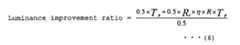
In the above equation, Tp, Rs, η and R are the polarizedlight p transmissivity, the polarized light s refractiveindex, the polarization s/p conversion factor of apolarization splitting means and the ratio of therefractive index of a light guiding plate reflectionsurface to that of a conventional one, respectively. A divisor 0.5 of the denominator means that, of light emittedfrom the conventional light guiding plate, only polarizedlight p, that is, the half of the light is used.
If the polarization splitting means is composedof only dielectric gratings, the Tp, Rs and R of thedielectric grating are 0.85, 0.55 and 1, respectively(Tp=0.85, Rs=0.55 and R=1).
If in the polarization splitting means, amulti-layer film is formed on a dielectric grating, theTp, Rs and R of the dielectric grating are 0.9, 0.9 and1, respectively (Tp=0.9, Rs=0.9 and R=1).
If in the polarization splitting means, a metallicgrating is formed on a dielectric grating, the Tp, Rsand R of the dielectric grating are 0.75, 0.6 and 1,respectively (Tp=0.75, Rs=0.6 and R=1).
In the case where double-refraction phasedifferences are 40°, 60°, 70° and 85°, polarization s/pconversion factors η are 0.44, 0.66, 0.77 and 0.94 inthe case where double-refraction phase differences are40°, 60°, 70° and 85°, respectively.
As clearly seen from Fig. 46, it is found that theluminance improvement ratio is enhanced. If adouble-refraction phase difference of nearly 90° can beprovided, the luminance improvement ratio sometimesbecomes 1.6, which means luminance can be improved by 60%.
So far the polarization splitting means 10,polarization converting means 20 and reflection means30, which all are the components of the light guidingplate 1 of the present invention have been described.By appropriately combining these components, theluminance improvement ratio of the light guiding plate1 can be enhanced.
Next, the further improvement of such a lightguiding plate 1 is described.
If the light guiding plate 1 is used as a lightingdevice, uniform color distribution of light emitted fromthe light guiding plate is required. Since thepolarization splitting means 10 is a grating structure,a rainbow may occur due to its spectral effect when whitelight is inputted. However, since a plurality of segmentsof light is inputted to one point of the polarizationsplitting means 10 from many directions, a plurality ofsegments of light emitted from the polarization splittingmeans 10 are mixed and no rainbow occurs.
However, color is somewhat different depending onthe position in the polarization splitting means 10. Sucha color difference can be unified by appropriatelyselecting the polarization splitting characteristic ofthe polarization splitting means 10, that is, both polarization p transmissivity and polarization srefractive index, specifically, appropriately selectingthe grating period, groove depth of grating, etc., ofthe polarization splitting means.
In particular, luminance in a position near thelight source 2 is different from that in a position faraway from it the light source 2. Therefore, in the lightguiding plate 1 used in a lighting device for liquidcrystal display, attention is paid to the uniform colordistribution in addition to the adoption of the structuredescribed above.
Next, this color distribution unifying technologyis described.
Firstly, in the light guiding plate 1 so fardescribed, the polarization splitting means 10 has beena periodic structure whose grating period, groove depthof grating, etc., are uniform. However, in order to unifythe color distribution, the grating period, groove depthof grating, etc., must be changed depending on both theposition and the polarization splitting characteristicof the polarization splitting means 10, specifically,the wavelength dependency of polarization ptransmissivity and that of polarization s refractiveindex must be changed depending on its position.
This point is described with reference to a drawing. Fig. 47 shows the polarization splitting means havinga different grating period depending on its position.
The optical density on the side near the light source2 of the polarization splitting means 10 shown in Fig.47 is high, and the density decreases as a position getsaway from the light source 2. Therefore, as to thepolarization splitting characteristic of thepolarization splitting means 10, the period and groovedepth of the dielectric grating of the polarizationsplitting means 10 is selected in such a way thatpolarization p transmissivity is set low to TP1 and highto TP2 on the near side (left side of Fig. 48) and farside (right side of Fig. 48) of the light source,respectively, and that polarization s refractive indexis set high to RS1 and low to RS2 on the near side (leftside of Fig. 48) and far side (right side of Fig. 48)of the light source, respectively.
Thus, if on the near side of the light source 2,two segments of light PP01 and PS01 attempt to transmitthe polarization splitting means 10, PP1, being polarizedlight p, whose optical density is low, is transmittedand PS1, being polarized light s, is reflected at highrate. On the far side of the light source 2, PP2 beingpolarized light p, whose optical density is higher thanthat of ordinary light is transmitted, and PS2 being polarized light s is reflected at low rate. Thus,differences in optical density between far and near areasare corrected, and optical density can be unified betweenfar and near sides. In other words, luminance distributioncan be unified. By changing the period of the dielectricgrating of the polarization splitting means 10 dependingon a position thus, luminance factor can be unified.
Sometimes luminance factors in the left and rightend areas are different depending on the type of a lightsource. This point is described below with reference toa drawing. Fig. 48 shows a polarization splitting meansin which the shape of a dielectric grating varies dependingon a position. For the dielectric grating (in the fourththrough eighth preferred embodiments)/metallic grating(in the ninth preferred embodiment) of the polarizedsplitting means 10 described above to realize apolarization splitting function, it is preferable toinput light orthogonally to the dielectric/metallicgrating. Therefore, usually it is preferable to use abar light source (linear light source) 2 as shown in Fig.48A. For example, the cold cathode tube light sourcedescribed above corresponds to such a linear light source2. However, as a monochrome light source, etc., a pointlight source 2, such as an LED, is sometimes used. Inthis case, light is not orthogonally inputted in the left and right end areas. Therefore, in this case, apolarization splitting function is not sometimesperformed completely and luminance distribution may notbe uniform.
In that case, the dielectric/metallic gratingis formed in a curved shape, as shown in Fig. 48B.Alternatively, the dielectric/metallic grating is formedin an approximate shape obtained by combining threestraight lines orthogonal to input light, as shown inFig. 48C. Since all segments of light and most segmentsof light enter orthogonally to the forming direction ofa grating structure in the curved grating structure shownin 46A and in the approximate-shaped grating structureshown in Fig. 48B, respectively, luminance distributioncan be unified between the left and right areas even ifeither bar or point light source 2 is adopted.
Next, the fact that devising the reflection means30 can also unify luminance factors is described withreference to a drawing. Fig. 49 shows the reflection meanswhose printed pattern varies depending on its position.As has been conventionally known, a diffusive/reflectivematerial shown in Fig. 49 (Fig. 45 is the squint viewof Fig. 49) is printed in such a way that its densitybecomes high on the near side of the light source 2 andlow on the far side. In this way, luminance distribution can also be unified.
Alternatively, adopting a diffusive hologram asa reflection means can unify luminance distribution.Figs. 50 and 51 show reflection means adopting a diffusivehologram whose reflection direction varies depending onits position. The diffusive hologram described abovebranches/polarizes input light in a plurality ofdirections with a different strength in each directionand at high efficiency. By adopting and designing thisdiffusive hologram in such a way that the refractive indexin the upward reflecting direction shown in Fig. 50 islow and high on the near and far side of the light source,respectively, optical density can be unified, andaccordingly luminance distribution can be unified.
By multiply branching input light, a reflectiontype diffusive hologram can realize a light diffusioneffect. A reflection type diffusive hologram can beconventionally obtained by plating. Alternatively, byadopting a light branching direction as the directionof a polarization splitting surface, the direction oflight emitted from the polarization splitting surfacecan be converged into a prescribed range.
The diffusive hologram can also be realized by thedesigning method of an optical branching filter knownas Dammann method besides the methods described above. Alternatively, the diffusive hologram can realize adiffusion function by forming a volume hologramrefractive index distribution. Alternatively, thediffusive hologram using speckle diffusion disclosed inJapanese Patent Laid-open Nos. 53-42726 "Finder of aCamera" or 53-51755 "Speckle Diffusion Plate GeneratingDevice", can be used.
In the light guiding plate used in a lighting device,such as a liquid crystal display device, a light emittingdirection must be included in a prescribed angle range.Fig. 52 shows the emitting angle range of a light guidingplate for a lighting device. As shown in Fig. 52, emittingangle ranges in the x-and y-directions are different.
Therefore, each emitting angle range must be setby the printed pattern method, preferably the method usinga diffusive hologram, the designing method of an opticalbranching filter known as Dammann method, the method forrealizing a diffusion function by forming a volumehologram refractive index distribution or the methodusing speckle diffusion disclosed in Japanese PatentLaid-open Mo. 53-42726 "Finder of a Camera" and 53-51755"Speckle Diffusion Plate Generating Device" which havebeen described earlier as a reflection means.
Next, a liquid crystal display device using thelight guiding plate 1 described above is described. Fig. 53 shows the rough structure of the liquid crystal displaydevice. Fig. 54 is its AB cross section showing therelationship between a grating structure and light tobe transmitted.
As shown in Fig. 53, a liquid crystal displaydevice 4 comprises a light source 2, a light guiding plate1 and a liquid crystal panel 5. A structure where thelight source 2 is disposed on the side of the light guidingplate 1 is called "edge light type". This light guidingplate 1 is almost wedge-shaped. The light source 2 andthe light guiding plate 1 constitute a lighting device6. As shown in Figs. 53 and 54, this lighting device 6supplies light (31c through 34c) to the nearly planarliquid crystal panel 5. The light guiding plate 1incorporates the polarization splitting means 10,polarization converting means 20, reflection means 30and light guiding means 40, which have been all describedso far.
The light guiding means 40, made of transparentresin, guides light 3a inputted from the light source2, to the liquid crystal panel 5. The light guiding means40 embeds the polarization converting means, which isnot shown in Fig. 53 for convenience sake. In this example,the polarization splitting means 10 is a metallic grating131 (see Fig. 35) that is made of metal and is formed on a surface that emits light for lighting (31c through34c). The reflection means 30 is made of metal.
Next, the function of this liquid crystal displaydevice is described. Light emitted from the light source2 is inputted to the light guiding means 40. In Figs.53 and 54, the light source 2 is, for example, a coldcathode tube light source. Light 3a emitted from thislight source 2 (although in Figs 53 and 54, only light3a emitted obliquely to the lower right is shown forconvenience sake, in reality a plurality of segments oflight is inputted to the light guiding means 40) isinputted to the light guidingmeans 40. The surface throughwhich the light 3a from the light source 2 is inputtedto the light guiding means 40 and surfaces except forthat on the liquid crystal side 5 are provided with areflection means 30 (30a and 30b), being a reflectionplate made of metallic film, and a reflection means 30(30c and 30d), being a reflection plate made of themetallic film shown in Fig. 54. Since light is fullyreflected on the inner surface of the liquid crystal panel5 of the light guiding means 40 if an incidence angleis large, the light 3a inputted to the light guiding means40 is repeatedly reflected in the light guiding means40 to cause multi-reflection. For example, by providinga structure for diffusing or orienting input light on the inside/outside of the light guiding means 40 and thesurface of the reflection means 30, as described earlier,light lighting the liquid crystal panel 5 can be uniformlydistributed on a plane.
Fig. 53 is described below with reference to Fig.54. Light 3b (32b, 33b and 34b) inputted to a specificsurface of the polarization splitting means 10 from theinside of the light guiding means 40 at an angle wherelight is not fully reflected, enters the grating 131.In the polarization splitting means 10, a gratingstructure is formed (in Fig. 54, it is formed expandingin the horizontal direction). Of light 3b (32b, 33b and34b) inputted to the polarization splitting means 10,polarized components (31c through 34c) perpendicular tothe forming direction (horizontal direction) of thegrating structure of the polarization splitting means10 transmit the polarization splitting means 10.Polarized components in parallel to the forming directionof the grating structure of the polarization splittingmeans 10 are reflected. If the grating structure is ametallic grating made of aluminum, and its period p andgroove depth of grating are approximately 200nm andbetween 100nm and 200nm, respectively, thetransmissivity of linear polarized light (31c through34c) in the transmitting direction is between 80 and 85% in the visible wavelength range.
Most of polarized components (32a, 33a and 34a)in the reflecting direction are reflected, and thereflected light (32a, 33a and 34a) repeatsmulti-reflection in the light guiding means 40 again.
Thus, while the light (32a, 33a and 34a) reflectedby the polarization splitting means 10 repeats reflectionin the light guiding means 40, the polarization convertingmeans 20 converts its polarization status (by doublerefraction) to generate a plurality of segments of lighthaving a variety of polarization statuses (32b, 33b and34b) . Then, the plurality of segments of light enter thepolarization splitting means 10 again, and as describedearlier, only polarized components (31c through 34c)orthogonal to the forming direction of the gratingstructure of the polarization splitting means 10 transmitthe polarization splitting means 10.
The process described above is repeated and thelight 3a inputted to the light guiding plate from thelight source 2 is emitted to the liquid crystal panel5 from the light guiding plate 1 as polarized light p(31c through 34c) . The direction of the linear polarizedlight of the light (31c through 34c) described above isthe same as that of polarized light that transmits apolarization plate 51. Therefore, the light (31c through 34c) can be inputted to a liquid crystal plate 52 withoutbeing absorbed.
While the light (32a through 34a), being a polarizedcomponent s reflected thus by the polarization splittingmeans 10, repeats reflection in the light guiding means40, the polarization converting means 20, having doublerefraction, converts its polarization status to generatea plurality of segments of light 3b (32b through 34b)having a variety of polarization statuses (that is, havingpolarized components p/s, including a variety ofpolarization angles). Then, the light enters thepolarization splitting means 10 again, and as describedearlier, polarized components (31c through 34c)orthogonal to the forming direction of the gratingstructure of the polarization splitting means 10 cantransmit the polarization splitting means 10.
As a result, since polarized components p (31cthrough 34c) can transmit the polarization splittingmeans 10 and can light the liquid crystal panel 5, thelight 3a inputted to the light guiding plate 1 from thelight source 2 can be efficiently used.
Alternatively, part of the reflection means (30athrough 30d) can be a diffusive hologram consisting ofminute convex/concave parts and can diffuse/reflectlight emitted toward the polarization splitting means 10.
Furthermore, alternatively, a reflection film madeof compound the same as or different from that of gratingstructure on the front surface can be provided for theback surface of the light guiding means 30.
The structure of such a liquid crystal displaydevice is compared with that of the conventional one.
The structure of the liquid crystal display deviceshown in Figs. 53 and 54 differs from that of theconventional liquid crystal display device shown in Fig.65 in that it adopts a light guiding plate 1 with apolarization splitting means 10 for functioning on theprinciple described above, provided on the liquid crystalpanel 5 side surface of a light guiding means 40 and thatit adopts a polarization converting means 20 forprovidingdouble-refraction phase difference that meets theprescribed conditions 1, 2 and 3. The structure of theliquid crystal panel 5 is the same as that shown in Fig.65. Therefore, polarized components p can be efficientlyextracted and many of polarized components p that a liquidcrystal panel requires are inputted. Accordingly, thefront surface of the liquid crystal display device 4 isvery bright.
This liquid crystal display device has an advantageof fewer components. Fig. 55 compares this liquid crystal display device with the conventional one. Theconventional liquid crystal display device shown in Fig.55A requires a variety of components (a reflection plate,a light guiding plate, adiffusionplate, two prism sheets,a protection film and a liquid crystal panel), while theliquid crystal display device of the present inventionhas fewer components, which is an advantage.
Since light (31c through 34c) can be efficientlyinputted to a liquid crystal plate 52 compared with theconventional lighting device 6, power consumption canbe reduced by reducing the luminance of the emitting deviceof a light source, such as a cold cathode tube, etc. Asa result, either the life of the light source 2 can beextended or the number of emitting devices can be reduced.
The light guiding plate 1 used in the liquid crystaldisplay device 4 can be structured as shown in Fig. 1.This liquid crystal display device is described belowwith reference to Fig. 56.
In this preferred embodiment, the comprehensivestructure of a liquid crystal display device is basicallythe same as the liquid crystal display device 4 shownin Fig. 53. Inparticular, a grating structure using simpledielectric gratings or those coated with a multi-layerfilm is adopted as a polarization splitting means 10,and a printed pattern or a diffusive hologram is adopted as a reflection means 30. Although the reflection means30 is not wedge-shaped, it can be set in such a way asto diffuse/reflect light in the prescribed direction,using the printed pattern or the diffusive hologram.Therefore, the same effect as that of a wedge-shaped lightguiding plate can be obtained. Since the other pointsare the same as those of the liquid crystal display device4 shown in Fig. 53, their descriptions are omitted.
Thus, polarized components of light orthogonal tothis dielectric grating (polarized components p)transmit through a grating structure disposed on theoutput side of the light guiding means 40 and light theliquid crystal panel 5. The polarized components of lightin parallel to the grating (polarized components s) arereflected by this grating structure, are returned toinside the light guiding means 40 and are multiplyreflected between the reflection plate of the lightguiding means 40 and the grating structure. Thepolarization status of the light reflected by the gratingstructure thus is converted while being reflected in thelight guiding means 40 and a plurality of segments oflight each with a different polarization status isobtained. The plurality of segments of light enters thegrating structure again, and as described above, thepolarized components orthogonal to the grating structure (polarized components p) can be transmitted.
As a result, polarized components orthogonal tothe grating structure (polarized components p) cantransmit through this grating structure and can lighta target to be lit, and accordingly, light inputted toa light guiding means from a light source can beefficiently used.
Figs. 57 through 60 show the rough structures ofother preferred embodiments of the present invention.These are sequentially described below. However, thepresent invention is also applicable to a variety of liquidcrystal display devices, etc., other than those shownin Figs. 57 through 60.
Firstly, Fig. 57 shows the case where the presentinvention is applied to a directly-under lighting typeliquid crystal display. Light emitted from the lightsource 2, such as a fluorescent tube, etc., passes througha light guiding means 450 (concept including all the lightguiding plates 1 in the preferred embodiments describedabove; this is also used in the following preferredembodiments) and reaches a grating portion (conceptincluding all the grating structures in the preferredembodiments described above; this is also used in the following preferred embodiments).
Polarized light is divided into two polarizedcomponents on a grating surface, and one polarizedcomponent transmits through the grating and lights theliquid crystal panel 5. The other polarized componentis reflected on the grating and passes through the lightguiding means 450. This polarized component is reflectedin a light source unit 200 and passes through the lightguiding means 450 again. In this case, its polarizationstatus is converted and the converted polarized componentlights the liquid crystal panel 5.
Fig. 58 shows the case where the present inventionis applied to a liquid display device that collects naturallight from a liquid crystal surface. Light inputtedthrough a light collection unit 250 reaches a gratingportion 600 through the light guiding means 450. Polarizedlight is divided into two polarized components on thegrating surface of the grating portion 600, and onepolarized component transmits the grating and lights theliquid crystal panel 5. The other polarized componentis reflected on the grating and passes through the lightguiding means 450. This polarized component is reflectedin a light source unit 200 and passes through the lightguiding means 450 again. In this case, its polarizationstatus is converted and the converted polarized component lights the liquid crystal panel 5.
Fig. 59 shows the case where the present inventionis applied to a front light type liquid crystal displaydevice. Light emitted from the light source 2 is inputtedto and reflected on the top surface of the light guidingmeans 450 and is inputted to the grating portion 600.Polarized light is divided into two polarized componentson the grating surface of the grating portion 600. Onepolarized component transmits through the grating andlights the liquid crystal panel 5. The other polarizedcomponent is reflected on the grating and is returnedto the light guiding means 450. This polarized componentis repeatedly reflected in the light guiding means 450.Then, its polarization status is converted. Theconverted polarized component enters the grating againand lights the liquid crystal panel 5. Light going upwardthrough the liquid crystal panel 5 transmits through thegrating, enters the light guiding means 450 at a smallincidence angle and passes through it. Reference number30e represents a reflection mirror.
Fig. 60 shows the case where a liquid crystal/colorfilter layer 5A is inserted between a liquid crystalsubstrate 55 made of glass or resin and the light guidingmeans 450. In this case, a thin liquid crystal displaydevice can be obtained.
The operation of each of the preferred embodimentsshown in Figs. 57 through 60 is basically the same asthose of the preferred embodiments described above.
For the light source 2, a monochrome or whitepoint-shape light source, such as an LED light source,can also be used, which is not particularly mentionedin each preferred embodiment of the present inventiondescribed above.
Next, examples of actual devices are describedbelow. Firstly, example 1 is described. Example 1 is anactually manufactured polarization splitting means 10.
Fig. 61 shows the cross section of its dielectricgrating (SEM picture). Polycarbonate is molded into alight guiding means, and a dielectric grating is copiedon its surface. The grating period and groove depth ofgrating are 0.6µm and 0.32µm, respectively. Fig. 62 showsthe polarization splitting characteristic of thedielectric grating. Dotted /solid lines indicatecomputer simulation, and Δ /× marks indicate their actualmeasurement values. For the light source, a singlewavelength LED light source emitting light with emissionwavelengths of 550nm/600nm/630nm is used. Thecross-section double refractive index distribution ofthe light guiding plate 1 meets condition 2. Thiscorresponds to example 1 shown in Fig. 46.
A luminance improvement ratio is measured usinga light guiding plate 1 with such a structure as a textdevice. Fig. 63 shows the configuration of the test devicefor measuring a luminance improvement ratio. As shownin Fig. 63, a polarization splitting means 10, a reflectionmeans 30 and a polarization converting means are formedon the front and back surfaces, and in the inside,respectively, of the light guiding plate 1. Light fromthe light source 2 (LED light source) is applied to bothside surfaces of the light guiding plate 1.
The luminance of the light emitted from this lightguiding plate 1 is improved 20% compared with that ofthe conventional PMMA resin light guiding plate in thesame shape without a polarization splitting surface, andthe evaluation indicates a practical use level (indicatedby double-circle marks).
Next, example 2, which is another example of anactual device is described. Example 2 is anotherpolarization splitting means.
Fig. 64 shows the cross section of a dielectricgrating having a three-layer film (SEM picture). Apolycarbonate dielectric grating whose period is 0.6µmis formed as a light guiding means, and a three-layerfilm made of TiO2, SiO2 and TiO2 is formed into a gratingstructure by evaporation using SiO2 as a binder. For the light source, a white light source is used. Thecross-section double-refractive index distributionmeets condition 3. This corresponds to example 2 shownin Fig. 46.
A luminance improvement ratio was measured usinga light guiding plate 1 with such a structure as a testdevice. The test device is shown in Fig. 63. Apolarizationsplitting means 10, a reflection means 30 and apolarization converting means are formed on the frontand back surfaces, and in the inside, respectively, ofthe light guiding plate 1. Light from the white lightsource 2 (LED light source) is applied to both sidesurfaces of the light guiding plate 1. The luminance ofthe light emitted from this light guiding plate 1 isimproved 60% compared with that of the conventional PMMAresin light guiding plate in the same shape, without apolarization splitting surface, and the evaluationindicates a practical use level (indicated bydouble-circle marks).
As described above, in the present invention, byreturning polarized components that are prevented fromtransmitting a polarization plate, such as a liquidcrystal panel, etc. (polarized component s) to insidea light guiding means by a polarization splitting means,being a grating structure formed on the surface of the light guiding means, and by inputting the polarizedcomponents to the polarization splitting means again bya reflection means, being a reflection plate, whileconverting its linear polarization direction by apolarization converting means, polarized components thatcan be inputted to a liquid crystal panel, can be extracted.Therefore, the polarized component of light (polarizedcomponents s) that conventionally cannot be effectivelyused can be converted into and used as the polarizedcomponent of light p. Thus, a light guiding plate in whichthe number of components, such as, emitting devices, etc.,is reduced and whose power consumption is reduced, anda liquid crystal display device with such a light guidingplate can be realized.


