EP1334519B1 - Ball limiting metallurgy for input/outputs and methods of fabrication - Google Patents
Ball limiting metallurgy for input/outputs and methods of fabricationDownload PDFInfo
- Publication number
- EP1334519B1 EP1334519B1EP01942135AEP01942135AEP1334519B1EP 1334519 B1EP1334519 B1EP 1334519B1EP 01942135 AEP01942135 AEP 01942135AEP 01942135 AEP01942135 AEP 01942135AEP 1334519 B1EP1334519 B1EP 1334519B1
- Authority
- EP
- European Patent Office
- Prior art keywords
- blm
- input
- nitrogen
- vanadium
- output
- Prior art date
- Legal status (The legal status is an assumption and is not a legal conclusion. Google has not performed a legal analysis and makes no representation as to the accuracy of the status listed.)
- Expired - Lifetime
Links
Images


Classifications
- H—ELECTRICITY
- H01—ELECTRIC ELEMENTS
- H01L—SEMICONDUCTOR DEVICES NOT COVERED BY CLASS H10
- H01L24/00—Arrangements for connecting or disconnecting semiconductor or solid-state bodies; Methods or apparatus related thereto
- H01L24/01—Means for bonding being attached to, or being formed on, the surface to be connected, e.g. chip-to-package, die-attach, "first-level" interconnects; Manufacturing methods related thereto
- H01L24/02—Bonding areas ; Manufacturing methods related thereto
- H01L24/03—Manufacturing methods
- H—ELECTRICITY
- H01—ELECTRIC ELEMENTS
- H01L—SEMICONDUCTOR DEVICES NOT COVERED BY CLASS H10
- H01L24/00—Arrangements for connecting or disconnecting semiconductor or solid-state bodies; Methods or apparatus related thereto
- H01L24/01—Means for bonding being attached to, or being formed on, the surface to be connected, e.g. chip-to-package, die-attach, "first-level" interconnects; Manufacturing methods related thereto
- H01L24/02—Bonding areas ; Manufacturing methods related thereto
- H01L24/04—Structure, shape, material or disposition of the bonding areas prior to the connecting process
- H01L24/05—Structure, shape, material or disposition of the bonding areas prior to the connecting process of an individual bonding area
- H—ELECTRICITY
- H01—ELECTRIC ELEMENTS
- H01L—SEMICONDUCTOR DEVICES NOT COVERED BY CLASS H10
- H01L2224/00—Indexing scheme for arrangements for connecting or disconnecting semiconductor or solid-state bodies and methods related thereto as covered by H01L24/00
- H01L2224/01—Means for bonding being attached to, or being formed on, the surface to be connected, e.g. chip-to-package, die-attach, "first-level" interconnects; Manufacturing methods related thereto
- H01L2224/02—Bonding areas; Manufacturing methods related thereto
- H01L2224/04—Structure, shape, material or disposition of the bonding areas prior to the connecting process
- H01L2224/05—Structure, shape, material or disposition of the bonding areas prior to the connecting process of an individual bonding area
- H01L2224/05001—Internal layers
- H01L2224/0502—Disposition
- H01L2224/05022—Disposition the internal layer being at least partially embedded in the surface
- H—ELECTRICITY
- H01—ELECTRIC ELEMENTS
- H01L—SEMICONDUCTOR DEVICES NOT COVERED BY CLASS H10
- H01L2224/00—Indexing scheme for arrangements for connecting or disconnecting semiconductor or solid-state bodies and methods related thereto as covered by H01L24/00
- H01L2224/01—Means for bonding being attached to, or being formed on, the surface to be connected, e.g. chip-to-package, die-attach, "first-level" interconnects; Manufacturing methods related thereto
- H01L2224/02—Bonding areas; Manufacturing methods related thereto
- H01L2224/04—Structure, shape, material or disposition of the bonding areas prior to the connecting process
- H01L2224/05—Structure, shape, material or disposition of the bonding areas prior to the connecting process of an individual bonding area
- H01L2224/05001—Internal layers
- H01L2224/0502—Disposition
- H01L2224/05026—Disposition the internal layer being disposed in a recess of the surface
- H01L2224/05027—Disposition the internal layer being disposed in a recess of the surface the internal layer extending out of an opening
- H—ELECTRICITY
- H01—ELECTRIC ELEMENTS
- H01L—SEMICONDUCTOR DEVICES NOT COVERED BY CLASS H10
- H01L2224/00—Indexing scheme for arrangements for connecting or disconnecting semiconductor or solid-state bodies and methods related thereto as covered by H01L24/00
- H01L2224/01—Means for bonding being attached to, or being formed on, the surface to be connected, e.g. chip-to-package, die-attach, "first-level" interconnects; Manufacturing methods related thereto
- H01L2224/02—Bonding areas; Manufacturing methods related thereto
- H01L2224/04—Structure, shape, material or disposition of the bonding areas prior to the connecting process
- H01L2224/05—Structure, shape, material or disposition of the bonding areas prior to the connecting process of an individual bonding area
- H01L2224/05001—Internal layers
- H01L2224/05099—Material
- H01L2224/051—Material with a principal constituent of the material being a metal or a metalloid, e.g. boron [B], silicon [Si], germanium [Ge], arsenic [As], antimony [Sb], tellurium [Te] and polonium [Po], and alloys thereof
- H01L2224/05163—Material with a principal constituent of the material being a metal or a metalloid, e.g. boron [B], silicon [Si], germanium [Ge], arsenic [As], antimony [Sb], tellurium [Te] and polonium [Po], and alloys thereof the principal constituent melting at a temperature of greater than 1550°C
- H01L2224/05172—Vanadium [V] as principal constituent
- H—ELECTRICITY
- H01—ELECTRIC ELEMENTS
- H01L—SEMICONDUCTOR DEVICES NOT COVERED BY CLASS H10
- H01L2224/00—Indexing scheme for arrangements for connecting or disconnecting semiconductor or solid-state bodies and methods related thereto as covered by H01L24/00
- H01L2224/01—Means for bonding being attached to, or being formed on, the surface to be connected, e.g. chip-to-package, die-attach, "first-level" interconnects; Manufacturing methods related thereto
- H01L2224/02—Bonding areas; Manufacturing methods related thereto
- H01L2224/04—Structure, shape, material or disposition of the bonding areas prior to the connecting process
- H01L2224/05—Structure, shape, material or disposition of the bonding areas prior to the connecting process of an individual bonding area
- H01L2224/0554—External layer
- H01L2224/0556—Disposition
- H01L2224/05571—Disposition the external layer being disposed in a recess of the surface
- H01L2224/05572—Disposition the external layer being disposed in a recess of the surface the external layer extending out of an opening
- H—ELECTRICITY
- H01—ELECTRIC ELEMENTS
- H01L—SEMICONDUCTOR DEVICES NOT COVERED BY CLASS H10
- H01L2224/00—Indexing scheme for arrangements for connecting or disconnecting semiconductor or solid-state bodies and methods related thereto as covered by H01L24/00
- H01L2224/01—Means for bonding being attached to, or being formed on, the surface to be connected, e.g. chip-to-package, die-attach, "first-level" interconnects; Manufacturing methods related thereto
- H01L2224/10—Bump connectors; Manufacturing methods related thereto
- H01L2224/11—Manufacturing methods
- H01L2224/1147—Manufacturing methods using a lift-off mask
- H—ELECTRICITY
- H01—ELECTRIC ELEMENTS
- H01L—SEMICONDUCTOR DEVICES NOT COVERED BY CLASS H10
- H01L2224/00—Indexing scheme for arrangements for connecting or disconnecting semiconductor or solid-state bodies and methods related thereto as covered by H01L24/00
- H01L2224/01—Means for bonding being attached to, or being formed on, the surface to be connected, e.g. chip-to-package, die-attach, "first-level" interconnects; Manufacturing methods related thereto
- H01L2224/10—Bump connectors; Manufacturing methods related thereto
- H01L2224/12—Structure, shape, material or disposition of the bump connectors prior to the connecting process
- H01L2224/13—Structure, shape, material or disposition of the bump connectors prior to the connecting process of an individual bump connector
- H01L2224/13001—Core members of the bump connector
- H01L2224/13099—Material
- H01L2224/131—Material with a principal constituent of the material being a metal or a metalloid, e.g. boron [B], silicon [Si], germanium [Ge], arsenic [As], antimony [Sb], tellurium [Te] and polonium [Po], and alloys thereof
- H01L2224/13101—Material with a principal constituent of the material being a metal or a metalloid, e.g. boron [B], silicon [Si], germanium [Ge], arsenic [As], antimony [Sb], tellurium [Te] and polonium [Po], and alloys thereof the principal constituent melting at a temperature of less than 400°C
- H01L2224/13109—Indium [In] as principal constituent
- H—ELECTRICITY
- H01—ELECTRIC ELEMENTS
- H01L—SEMICONDUCTOR DEVICES NOT COVERED BY CLASS H10
- H01L2224/00—Indexing scheme for arrangements for connecting or disconnecting semiconductor or solid-state bodies and methods related thereto as covered by H01L24/00
- H01L2224/01—Means for bonding being attached to, or being formed on, the surface to be connected, e.g. chip-to-package, die-attach, "first-level" interconnects; Manufacturing methods related thereto
- H01L2224/10—Bump connectors; Manufacturing methods related thereto
- H01L2224/12—Structure, shape, material or disposition of the bump connectors prior to the connecting process
- H01L2224/13—Structure, shape, material or disposition of the bump connectors prior to the connecting process of an individual bump connector
- H01L2224/13001—Core members of the bump connector
- H01L2224/13099—Material
- H01L2224/131—Material with a principal constituent of the material being a metal or a metalloid, e.g. boron [B], silicon [Si], germanium [Ge], arsenic [As], antimony [Sb], tellurium [Te] and polonium [Po], and alloys thereof
- H01L2224/13101—Material with a principal constituent of the material being a metal or a metalloid, e.g. boron [B], silicon [Si], germanium [Ge], arsenic [As], antimony [Sb], tellurium [Te] and polonium [Po], and alloys thereof the principal constituent melting at a temperature of less than 400°C
- H01L2224/13111—Tin [Sn] as principal constituent
- H—ELECTRICITY
- H01—ELECTRIC ELEMENTS
- H01L—SEMICONDUCTOR DEVICES NOT COVERED BY CLASS H10
- H01L24/00—Arrangements for connecting or disconnecting semiconductor or solid-state bodies; Methods or apparatus related thereto
- H01L24/01—Means for bonding being attached to, or being formed on, the surface to be connected, e.g. chip-to-package, die-attach, "first-level" interconnects; Manufacturing methods related thereto
- H01L24/10—Bump connectors ; Manufacturing methods related thereto
- H01L24/11—Manufacturing methods
- H—ELECTRICITY
- H01—ELECTRIC ELEMENTS
- H01L—SEMICONDUCTOR DEVICES NOT COVERED BY CLASS H10
- H01L24/00—Arrangements for connecting or disconnecting semiconductor or solid-state bodies; Methods or apparatus related thereto
- H01L24/01—Means for bonding being attached to, or being formed on, the surface to be connected, e.g. chip-to-package, die-attach, "first-level" interconnects; Manufacturing methods related thereto
- H01L24/10—Bump connectors ; Manufacturing methods related thereto
- H01L24/12—Structure, shape, material or disposition of the bump connectors prior to the connecting process
- H01L24/13—Structure, shape, material or disposition of the bump connectors prior to the connecting process of an individual bump connector
- H—ELECTRICITY
- H01—ELECTRIC ELEMENTS
- H01L—SEMICONDUCTOR DEVICES NOT COVERED BY CLASS H10
- H01L2924/00—Indexing scheme for arrangements or methods for connecting or disconnecting semiconductor or solid-state bodies as covered by H01L24/00
- H01L2924/0001—Technical content checked by a classifier
- H01L2924/00013—Fully indexed content
- H—ELECTRICITY
- H01—ELECTRIC ELEMENTS
- H01L—SEMICONDUCTOR DEVICES NOT COVERED BY CLASS H10
- H01L2924/00—Indexing scheme for arrangements or methods for connecting or disconnecting semiconductor or solid-state bodies as covered by H01L24/00
- H01L2924/01—Chemical elements
- H01L2924/01005—Boron [B]
- H—ELECTRICITY
- H01—ELECTRIC ELEMENTS
- H01L—SEMICONDUCTOR DEVICES NOT COVERED BY CLASS H10
- H01L2924/00—Indexing scheme for arrangements or methods for connecting or disconnecting semiconductor or solid-state bodies as covered by H01L24/00
- H01L2924/01—Chemical elements
- H01L2924/01006—Carbon [C]
- H—ELECTRICITY
- H01—ELECTRIC ELEMENTS
- H01L—SEMICONDUCTOR DEVICES NOT COVERED BY CLASS H10
- H01L2924/00—Indexing scheme for arrangements or methods for connecting or disconnecting semiconductor or solid-state bodies as covered by H01L24/00
- H01L2924/01—Chemical elements
- H01L2924/01013—Aluminum [Al]
- H—ELECTRICITY
- H01—ELECTRIC ELEMENTS
- H01L—SEMICONDUCTOR DEVICES NOT COVERED BY CLASS H10
- H01L2924/00—Indexing scheme for arrangements or methods for connecting or disconnecting semiconductor or solid-state bodies as covered by H01L24/00
- H01L2924/01—Chemical elements
- H01L2924/01015—Phosphorus [P]
- H—ELECTRICITY
- H01—ELECTRIC ELEMENTS
- H01L—SEMICONDUCTOR DEVICES NOT COVERED BY CLASS H10
- H01L2924/00—Indexing scheme for arrangements or methods for connecting or disconnecting semiconductor or solid-state bodies as covered by H01L24/00
- H01L2924/01—Chemical elements
- H01L2924/01018—Argon [Ar]
- H—ELECTRICITY
- H01—ELECTRIC ELEMENTS
- H01L—SEMICONDUCTOR DEVICES NOT COVERED BY CLASS H10
- H01L2924/00—Indexing scheme for arrangements or methods for connecting or disconnecting semiconductor or solid-state bodies as covered by H01L24/00
- H01L2924/01—Chemical elements
- H01L2924/0102—Calcium [Ca]
- H—ELECTRICITY
- H01—ELECTRIC ELEMENTS
- H01L—SEMICONDUCTOR DEVICES NOT COVERED BY CLASS H10
- H01L2924/00—Indexing scheme for arrangements or methods for connecting or disconnecting semiconductor or solid-state bodies as covered by H01L24/00
- H01L2924/01—Chemical elements
- H01L2924/01022—Titanium [Ti]
- H—ELECTRICITY
- H01—ELECTRIC ELEMENTS
- H01L—SEMICONDUCTOR DEVICES NOT COVERED BY CLASS H10
- H01L2924/00—Indexing scheme for arrangements or methods for connecting or disconnecting semiconductor or solid-state bodies as covered by H01L24/00
- H01L2924/01—Chemical elements
- H01L2924/01023—Vanadium [V]
- H—ELECTRICITY
- H01—ELECTRIC ELEMENTS
- H01L—SEMICONDUCTOR DEVICES NOT COVERED BY CLASS H10
- H01L2924/00—Indexing scheme for arrangements or methods for connecting or disconnecting semiconductor or solid-state bodies as covered by H01L24/00
- H01L2924/01—Chemical elements
- H01L2924/01024—Chromium [Cr]
- H—ELECTRICITY
- H01—ELECTRIC ELEMENTS
- H01L—SEMICONDUCTOR DEVICES NOT COVERED BY CLASS H10
- H01L2924/00—Indexing scheme for arrangements or methods for connecting or disconnecting semiconductor or solid-state bodies as covered by H01L24/00
- H01L2924/01—Chemical elements
- H01L2924/01029—Copper [Cu]
- H—ELECTRICITY
- H01—ELECTRIC ELEMENTS
- H01L—SEMICONDUCTOR DEVICES NOT COVERED BY CLASS H10
- H01L2924/00—Indexing scheme for arrangements or methods for connecting or disconnecting semiconductor or solid-state bodies as covered by H01L24/00
- H01L2924/01—Chemical elements
- H01L2924/01033—Arsenic [As]
- H—ELECTRICITY
- H01—ELECTRIC ELEMENTS
- H01L—SEMICONDUCTOR DEVICES NOT COVERED BY CLASS H10
- H01L2924/00—Indexing scheme for arrangements or methods for connecting or disconnecting semiconductor or solid-state bodies as covered by H01L24/00
- H01L2924/01—Chemical elements
- H01L2924/01041—Niobium [Nb]
- H—ELECTRICITY
- H01—ELECTRIC ELEMENTS
- H01L—SEMICONDUCTOR DEVICES NOT COVERED BY CLASS H10
- H01L2924/00—Indexing scheme for arrangements or methods for connecting or disconnecting semiconductor or solid-state bodies as covered by H01L24/00
- H01L2924/01—Chemical elements
- H01L2924/01049—Indium [In]
- H—ELECTRICITY
- H01—ELECTRIC ELEMENTS
- H01L—SEMICONDUCTOR DEVICES NOT COVERED BY CLASS H10
- H01L2924/00—Indexing scheme for arrangements or methods for connecting or disconnecting semiconductor or solid-state bodies as covered by H01L24/00
- H01L2924/01—Chemical elements
- H01L2924/01057—Lanthanum [La]
- H—ELECTRICITY
- H01—ELECTRIC ELEMENTS
- H01L—SEMICONDUCTOR DEVICES NOT COVERED BY CLASS H10
- H01L2924/00—Indexing scheme for arrangements or methods for connecting or disconnecting semiconductor or solid-state bodies as covered by H01L24/00
- H01L2924/01—Chemical elements
- H01L2924/01073—Tantalum [Ta]
- H—ELECTRICITY
- H01—ELECTRIC ELEMENTS
- H01L—SEMICONDUCTOR DEVICES NOT COVERED BY CLASS H10
- H01L2924/00—Indexing scheme for arrangements or methods for connecting or disconnecting semiconductor or solid-state bodies as covered by H01L24/00
- H01L2924/01—Chemical elements
- H01L2924/01074—Tungsten [W]
- H—ELECTRICITY
- H01—ELECTRIC ELEMENTS
- H01L—SEMICONDUCTOR DEVICES NOT COVERED BY CLASS H10
- H01L2924/00—Indexing scheme for arrangements or methods for connecting or disconnecting semiconductor or solid-state bodies as covered by H01L24/00
- H01L2924/01—Chemical elements
- H01L2924/01076—Osmium [Os]
- H—ELECTRICITY
- H01—ELECTRIC ELEMENTS
- H01L—SEMICONDUCTOR DEVICES NOT COVERED BY CLASS H10
- H01L2924/00—Indexing scheme for arrangements or methods for connecting or disconnecting semiconductor or solid-state bodies as covered by H01L24/00
- H01L2924/01—Chemical elements
- H01L2924/01078—Platinum [Pt]
- H—ELECTRICITY
- H01—ELECTRIC ELEMENTS
- H01L—SEMICONDUCTOR DEVICES NOT COVERED BY CLASS H10
- H01L2924/00—Indexing scheme for arrangements or methods for connecting or disconnecting semiconductor or solid-state bodies as covered by H01L24/00
- H01L2924/01—Chemical elements
- H01L2924/01079—Gold [Au]
- H—ELECTRICITY
- H01—ELECTRIC ELEMENTS
- H01L—SEMICONDUCTOR DEVICES NOT COVERED BY CLASS H10
- H01L2924/00—Indexing scheme for arrangements or methods for connecting or disconnecting semiconductor or solid-state bodies as covered by H01L24/00
- H01L2924/01—Chemical elements
- H01L2924/01082—Lead [Pb]
- H—ELECTRICITY
- H01—ELECTRIC ELEMENTS
- H01L—SEMICONDUCTOR DEVICES NOT COVERED BY CLASS H10
- H01L2924/00—Indexing scheme for arrangements or methods for connecting or disconnecting semiconductor or solid-state bodies as covered by H01L24/00
- H01L2924/013—Alloys
- H01L2924/0132—Binary Alloys
- H01L2924/01322—Eutectic Alloys, i.e. obtained by a liquid transforming into two solid phases
- H—ELECTRICITY
- H01—ELECTRIC ELEMENTS
- H01L—SEMICONDUCTOR DEVICES NOT COVERED BY CLASS H10
- H01L2924/00—Indexing scheme for arrangements or methods for connecting or disconnecting semiconductor or solid-state bodies as covered by H01L24/00
- H01L2924/013—Alloys
- H01L2924/0132—Binary Alloys
- H01L2924/01327—Intermediate phases, i.e. intermetallics compounds
- H—ELECTRICITY
- H01—ELECTRIC ELEMENTS
- H01L—SEMICONDUCTOR DEVICES NOT COVERED BY CLASS H10
- H01L2924/00—Indexing scheme for arrangements or methods for connecting or disconnecting semiconductor or solid-state bodies as covered by H01L24/00
- H01L2924/013—Alloys
- H01L2924/014—Solder alloys
- H—ELECTRICITY
- H01—ELECTRIC ELEMENTS
- H01L—SEMICONDUCTOR DEVICES NOT COVERED BY CLASS H10
- H01L2924/00—Indexing scheme for arrangements or methods for connecting or disconnecting semiconductor or solid-state bodies as covered by H01L24/00
- H01L2924/10—Details of semiconductor or other solid state devices to be connected
- H01L2924/11—Device type
- H01L2924/14—Integrated circuits
- H01L2924/143—Digital devices
- H01L2924/1433—Application-specific integrated circuit [ASIC]
- H—ELECTRICITY
- H01—ELECTRIC ELEMENTS
- H01L—SEMICONDUCTOR DEVICES NOT COVERED BY CLASS H10
- H01L2924/00—Indexing scheme for arrangements or methods for connecting or disconnecting semiconductor or solid-state bodies as covered by H01L24/00
- H01L2924/15—Details of package parts other than the semiconductor or other solid state devices to be connected
- H01L2924/151—Die mounting substrate
- H01L2924/156—Material
- H01L2924/15786—Material with a principal constituent of the material being a non metallic, non metalloid inorganic material
- H01L2924/15787—Ceramics, e.g. crystalline carbides, nitrides or oxides
- H—ELECTRICITY
- H01—ELECTRIC ELEMENTS
- H01L—SEMICONDUCTOR DEVICES NOT COVERED BY CLASS H10
- H01L2924/00—Indexing scheme for arrangements or methods for connecting or disconnecting semiconductor or solid-state bodies as covered by H01L24/00
- H01L2924/19—Details of hybrid assemblies other than the semiconductor or other solid state devices to be connected
- H01L2924/1901—Structure
- H01L2924/1904—Component type
- H01L2924/19041—Component type being a capacitor
- H—ELECTRICITY
- H01—ELECTRIC ELEMENTS
- H01L—SEMICONDUCTOR DEVICES NOT COVERED BY CLASS H10
- H01L2924/00—Indexing scheme for arrangements or methods for connecting or disconnecting semiconductor or solid-state bodies as covered by H01L24/00
- H01L2924/19—Details of hybrid assemblies other than the semiconductor or other solid state devices to be connected
- H01L2924/1901—Structure
- H01L2924/1904—Component type
- H01L2924/19043—Component type being a resistor
- H—ELECTRICITY
- H01—ELECTRIC ELEMENTS
- H01L—SEMICONDUCTOR DEVICES NOT COVERED BY CLASS H10
- H01L2924/00—Indexing scheme for arrangements or methods for connecting or disconnecting semiconductor or solid-state bodies as covered by H01L24/00
- H01L2924/30—Technical effects
- H01L2924/301—Electrical effects
- H01L2924/30107—Inductance
- Y—GENERAL TAGGING OF NEW TECHNOLOGICAL DEVELOPMENTS; GENERAL TAGGING OF CROSS-SECTIONAL TECHNOLOGIES SPANNING OVER SEVERAL SECTIONS OF THE IPC; TECHNICAL SUBJECTS COVERED BY FORMER USPC CROSS-REFERENCE ART COLLECTIONS [XRACs] AND DIGESTS
- Y10—TECHNICAL SUBJECTS COVERED BY FORMER USPC
- Y10T—TECHNICAL SUBJECTS COVERED BY FORMER US CLASSIFICATION
- Y10T428/00—Stock material or miscellaneous articles
- Y10T428/12—All metal or with adjacent metals
- Y10T428/12493—Composite; i.e., plural, adjacent, spatially distinct metal components [e.g., layers, joint, etc.]
- Y10T428/12535—Composite; i.e., plural, adjacent, spatially distinct metal components [e.g., layers, joint, etc.] with additional, spatially distinct nonmetal component
- Y10T428/12556—Organic component
Definitions
- the present inventionrelates to the field of semiconductor Integrated Circuits (IC), and more specifically, to a bump limiting metallurgy (BLM) for input/ output of a device.
- ICsemiconductor Integrated Circuits
- BBMbump limiting metallurgy
- Input/ outputsare used in a device to condition and distribute power, ground, and signals.
- the I/Oscan be wirebonded to a package or board with leads formed from Gold (Au) or Copper (Cu) wire.
- AuGold
- CuCopper
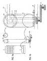
- FIG. 1 (a) and Figure 1 (b)show a solder bump 15 with a diameter 1 and a pitch 2.
- the solder bump 15is formed on Ball Limiting Metallurgy (BLM) 14.
- BLMis also known as Pad Limiting Metallurgy (PLM) or Under Bump Metallurgy (UBM).
- PLMPad Limiting Metallurgy
- UBMUnder Bump Metallurgy
- the BLM 14is connected through a via 12 in the passivation layer 13 to an underlying bond pad 11b.
- the passivation layer 13,comprises one or more layers of materials, such as silicon oxide, silicon nitride, or polyimide, which act as a barrier to moisture, ions, or contaminants.
- the bond pad 11bis a widened portion of a metal line 11a in the top metal layer of the device.
- the line 11ais connected to an underlying via 10 that is, in turn, connected to an underlying line 9.
- a devicetypically has 2 to 8 metal layers so a via and a line are alternated vertically until electrical contact is made to the desired part of the IC or the substrate below.
- Figure 1 (a) and Figure 1 (b)show an areal array 3 of bumps 15 across the entire active area of the chip.
- the array 3is substantially periodic and may be face-centered cubic or hexagonal to achieve a higher density of bumps 15.
- a bumped deviceis turned over and packaged as a Flip Chip (FC).
- FCFlip Chip
- a solder bump technology based on Controlled Collapse Chip Connection (C4)may be used for Direct Chip Attach (DCA) to conductive traces on a package or circuit board.
- the circuit boardmay be a ceramic substrate, Printed Wiring Board (PWB), flexible circuit, or a silicon substrate. Bumping a device also reduces the resistance and inductance in the I/Os thus significantly improving performance.
- a high performance devicesuch as a microprocessor, an Application Specific Integrated Circuit (ASIC), a Field Programmable Gate Array (FPGA), or a System-on-a-Chip (SOC), may have about 600 to 7000 I/Os so the I/Os need to be scaled down to limit die size.
- Wirebondingmay involve a pitch of less than 60 microns using wires with a diameter of less than 25 microns with ball bonds of less than 40 microns.
- Bumpingmay involve bumps with a diameter of about 45 to 90 microns and a pitch of about 125 to 300 microns.
- I/Osmay fail if junction temperature exceeds 100 to 125 degrees C or current density exceeds 150 to 425 milliamperes per I/O.
- Electromigration or thermomigrationcan increase resistance by over 2 orders of magnitude before finally resulting in an open circuit. Elevated temperatures can also cause inter-diffusion of metals. The resultant intermetallic alloys are brittle and may be susceptible to stress cracking. A mismatch in the Coefficient of Thermal Expansion (CTE) can result in large shear stresses on a wire lead or bump.
- CTECoefficient of Thermal Expansion
- solderhas a CTE of about 30 ppm/degree C compared with about 7 ppm/degree C for a ceramic substrate and about 5 ppm/degree C for a Silicon substrate.
- a wire lead or bumpmay fail from thermal shock if the thermal ramp rate exceeds about 15 to 20 degrees C/minute. Thermal cycling at lower thermal ramp rates may also cause a wire lead or bump to crack due to fatigue induced by elastic deformation or creep deformation.
- an input/output for a semiconductor integrated circuit device as claimed in claim 1 hereinthere is provided an input/output for a semiconductor integrated circuit device as claimed in claim 1 herein.
- the present inventionare novel ball limiting metallurgies (BLM) for input/outputs (I/Os) for devices and their methods of fabrication. From WO 99/344 23 ball limiting metallurgies (BLM) are known comprising a nickel-vanadium alloy film.
- BBMball limiting metallurgies
- the present inventionare a novel barrier layer metals or ball limiting metallurgy (BLM) for input/outputs to a device such as semiconductor devices.
- an input/output deviceincludes a bond pad having a ball limiting metallurgy (BLM) formed thereon and a bump on the BLM.
- the ball limiting metallurgy (BLM)comprises a first alloy film comprising nickel-vanadium-nitrogen.
- the ball limiting metallurgy (BLM)may comprise a nickel niobium alloy film.
- the input/output (I/O) of the present inventionis ideally suited for providing the inputting and outputting of electrical signals to a semiconductor device or integrated circuit such as a microprocessor, memory, application are known comprising a nickel-vanadium alloy film. specific integrated circuit (ASIC), field programmable gate arrays (FPGA) and especially where a large number of I/Os are required (e.g., 600-7000 I/Os).
- ASICapplication specific integrated circuit
- FPGAfield programmable gate arrays
- Device 200includes a semiconductor substrate such as a silicon substrate 202 having a plurality of active features 204 such as transistors and capacitors formed thereon.
- the active features 204are coupled together into functional circuits through multiple levels of interconnects 206 isolated from one another by interlayer dielectrics (ILD) 207.
- ILDinterlayer dielectrics
- Electrical contacts or vias 208electrically couple the different levels of interconnects through ILD 207.
- Metal interconnectsare typically formed of a low resistance metal such as aluminum, aluminum doped with copper and copper.
- Contacts and vias 206are typically formed with tungsten but can formed with other materials such as copper.
- the upper most level of metalizationincludes interconnects 206 and bond pads 212. Bond pads (or landing pads) 212 are widened portions of the upper most level of metalization to which electrical contact to external devices are made to semiconductor device 200.
- a typical passivation layer 214includes a lower hermetic silicon nitride layer 216 to provide hermetic sealing of device 200 and an upper polyimide layer 218 for providing scratch protection.
- an opening 220is formed through passivation layer 214 as shown in Figure 2b to expose a portion of bond pad 212.
- Opening 220can be formed utilizing a photoresist layer and well-know photolithography and etching techniques.
- opening 220can be formed in passivation layer 214 by utilizing a photo definable polyimide film 218.
- a ball limiting metallurgyis blanket deposited over passivation film 218 and into opening 220 and onto bond pad 212 as shown in Figure 2c .
- the ball limiting metallurgy (BLM) 222 layerincludes a lower adhesion layer 224 which provides good adhesion to bond pad 212 and passivation layer 214.
- the lowered adhesion layer 224maybe formed from titanium (Ti) with a thickness of about 200-1500 ⁇ .
- Other possible metals for adhesion layer 224include but are not limited to titanium tungsten (TiW), tantalum (Ta), or chromium (Cr). Any well-known techniques such as sputtering can be used to deposit adhesion layer 224.
- the ball limiting metallurgyincludes an upper layer 226 which is wettable by solder.
- the upper lay 226is a film consisting of nickel, vanadium, and nitrogen. Nitrogen is added to the film to lock the vanadium with nitrogen so that it cannot react with oxygen and degrade the reliability of the BLM.
- the upper layer 226includes a suitable amount of nitrogen to sufficiently prevent the oxidation of vanadium in the upper film 226.
- the upper filmincludes as much nitrogen as vanadium.
- the upper film 226includes about 8 atomic percent vanadium, about 8 atomic percent nitrogen, and the remainder nickel.
- the upper nickel-vanadium-nitrogen alloy film 226can have a thickness between 1000-4000 ⁇ .
- a suitable nickel-vanadium-nitrogen alloy film 226can be formed by reactive sputtered utilizing a nickel-vanadium target in an ambient containing nitrogen.
- the nickel-vanadium-nitrogen film 226is formed by magnetic sputtering with Argon (Ar) from a nickel-vanadium target in a magnetron sputter chamber, such as manufactured by Material Research Corporation (MRC) while nitrogen gas (N 2 ) is fed into the chamber. No oxygen is present in the chamber during sputtering. Nitrogen (N 2 ) gas is fed in at a rate sufficient to saturate the deposited film 226 with nitrogen.
- N 2is fed into a magnetron sputter chamber at a rate between 15- 30 sccms.
- the upper layer of 226 of BLM 222is a nickel-niobium (Ni-Nb) alloy.
- the upper layer 226is a nickel-niobium (Ni-Nb) alloy having approximately 10 atomic percent niobium (Nb) with the remainder nickel (Ni).
- Ni-Nbnickel-niobium
- a nickel-niobium (Ni-Nb) alloy having a thickness between 1000-4000 ⁇can be used.
- a suitable nickel-niobium (Ni-Nb) filmcan be formed by any well-known method such as by sputtering from a nickel-niobium (Ni-Nb) target.
- a nickel-niobium (Ni-Nb) upper film 226has shown good reliability.
- the BLM 222acts a diffusion barrier to metals. Depending upon the type of metallurgy selected for bumps and the BLM, additional layers may be inserted between the adhesion 224 and the upper layer 226.
- the intermediate layer usedmust have good adhesion to both the adhesion layer 224 and the upper layer 226.
- a bump 228is formed on BLM layer 222 over bond pad 212.
- a bump 228can be formed, by for example, forming a photoresist mask 230 having an opening to expose the BLM layer over a bond pad as shown in Figure 2d .
- Solderis then electroplated onto the BLM 222 as shown in Figure 2d .
- the solderforms a mushroom shape as shown in Figure 2d .
- the soldermay be from lead tin (Pb-Sn) or lead indium (Pb-In). Tin prevents oxidation and strengthens the bonding to the BLM 222.
- the use of nickel (Ni) in the upper 226 BLM layer 222enables the plating of lead.
- the substrateis heated in an oven or furnace to reflow the solder into a solder bump 228 as shown in Figure 2f .
- the melting temperature of the solder in bump 228depends upon the types of metal selected on their relative concentrations. For example, a high lead solder such as 95 Pb/5 Sn by weight reflows at about 300-360°C while in an eutectic solder such as 37 Pb/63 Sn reflows at about 180-240°C.
- the reflowed bump 228can be connected to a corresponding bump on a package or board.
- the bump on the package or boardis formed from Tin (Sn) or solder with a relatively low melting temperature such as 160°C so that bump 228 on the chip will not reflow during the chip attachment process.
- the novel input/outputs of the present invention and their methods of fabricationenables the fabrication of a large number (between 600-7000 I/Os) across the upper surface of device 200.
- the I/Os of the present inventioncan support current density of between 200-300 milli-amps per bump, and can withstand operating temperature between 110-120°C without reliability issues.
- the input/output of the present inventionenables the fabrication of semiconductor devices which require large numbers of I/Os.
Landscapes
- Engineering & Computer Science (AREA)
- Computer Hardware Design (AREA)
- Microelectronics & Electronic Packaging (AREA)
- Power Engineering (AREA)
- Manufacturing & Machinery (AREA)
- Wire Bonding (AREA)
- Internal Circuitry In Semiconductor Integrated Circuit Devices (AREA)
- Electric Connection Of Electric Components To Printed Circuits (AREA)
- Conductive Materials (AREA)
- Pens And Brushes (AREA)
- Adornments (AREA)
- Dental Preparations (AREA)
Abstract
Description
- The present invention relates to the field of semiconductor Integrated Circuits (IC), and more specifically, to a bump limiting metallurgy (BLM) for input/ output of a device.
- Input/ outputs are used in a device to condition and distribute power, ground, and signals. The I/Os can be wirebonded to a package or board with leads formed from Gold (Au) or Copper (Cu) wire. However, when the number of ' I/Os reaches about 400 to 1000, bumping often becomes more advantageous than wirebonding.
Figure 1 (a) and Figure 1 (b) show asolder bump 15 with a diameter 1 and apitch 2. Thesolder bump 15 is formed on Ball Limiting Metallurgy (BLM)14. BLM is also known as Pad Limiting Metallurgy (PLM) or Under Bump Metallurgy (UBM). The BLM14 is connected through avia 12 in thepassivation layer 13 to anunderlying bond pad 11b. Thepassivation layer 13, comprises one or more layers of materials, such as silicon oxide, silicon nitride, or polyimide, which act as a barrier to moisture, ions, or contaminants. Thebond pad 11b is a widened portion of a metal line11a in the top metal layer of the device. The line11a is connected to an underlying via10 that is, in turn, connected to an underlying line 9. A device typically has 2 to 8 metal layers so a via and a line are alternated vertically until electrical contact is made to the desired part of the IC or the substrate below.- Bumping can significantly improve access to the core area and maximize utilization of the silicon area.
Figure 1 (a) andFigure 1 (b) show anareal array 3 ofbumps 15 across the entire active area of the chip. Thearray 3 is substantially periodic and may be face-centered cubic or hexagonal to achieve a higher density ofbumps 15. A bumped device is turned over and packaged as a Flip Chip (FC). A solder bump technology based on Controlled Collapse Chip Connection (C4) may be used for Direct Chip Attach (DCA) to conductive traces on a package or circuit board. The circuit board may be a ceramic substrate, Printed Wiring Board (PWB), flexible circuit, or a silicon substrate. Bumping a device also reduces the resistance and inductance in the I/Os thus significantly improving performance. - A high performance device, such as a microprocessor, an Application Specific Integrated Circuit (ASIC), a Field Programmable Gate Array (FPGA), or a System-on-a-Chip (SOC), may have about 600 to 7000 I/Os so the I/Os need to be scaled down to limit die size. Wirebonding may involve a pitch of less than 60 microns using wires with a diameter of less than 25 microns with ball bonds of less than 40 microns. Bumping may involve bumps with a diameter of about 45 to 90 microns and a pitch of about 125 to 300 microns.
- Power management and thermal management become very critical when wire leads or bumps are scaled down. I/Os may fail if junction temperature exceeds 100 to 125 degrees C or current density exceeds 150 to 425 milliamperes per I/O. Electromigration or thermomigration can increase resistance by over 2 orders of magnitude before finally resulting in an open circuit. Elevated temperatures can also cause inter-diffusion of metals. The resultant intermetallic alloys are brittle and may be susceptible to stress cracking. A mismatch in the Coefficient of Thermal Expansion (CTE) can result in large shear stresses on a wire lead or bump. For example, solder has a CTE of about 30 ppm/degree C compared with about 7 ppm/degree C for a ceramic substrate and about 5 ppm/degree C for a Silicon substrate. A wire lead or bump may fail from thermal shock if the thermal ramp rate exceeds about 15 to 20 degrees C/minute. Thermal cycling at lower thermal ramp rates may also cause a wire lead or bump to crack due to fatigue induced by elastic deformation or creep deformation.
- Thus, the failure of I/Os, especially the power I/Os, due to high currents and high temperatures is a major concern.
- According to a first aspect of this invention there is provided an input/output for a semiconductor integrated circuit device as claimed in claim 1 herein.
- According to a second aspect of the invention there is provided a method as claimed in claim 8 herein.
- Preferred features of the invention are defined by the dependent claims.
Figure 1a is an illustration of a plain view of a prior art bump.Figure 1b is an illustration of a cross-sectional view of a prior bump.Figure 2a is an illustration of a cross-sectional view of a portion of semiconductor device.Figure 2b is an illustration of cross-sectional view showing the formation of an opening over a bond pad in the device ofFigure 2a .Figure 2c is an illustration of a cross-sectional view showing a formation of a ball limiting metallurgy (BLM) on a device ofFigure 2b .Figure 2d is an illustration of a cross-section view showing the formation of a bump on the device ofFigure 2c .Figure 2e is an illustration of a cross-sectional view showing the removal of exposed portions of the BLM layer from the device ofFigure 2d .Figure 2f is an illustration of a cross-sectional view showing the reflow of the bump on the device ofFigure 2e .- The present invention are novel ball limiting metallurgies (BLM) for input/outputs (I/Os) for devices and their methods of fabrication. From
WO 99/344 23 - The present invention are a novel barrier layer metals or ball limiting metallurgy (BLM) for input/outputs to a device such as semiconductor devices. According to an embodiment of the present invention an input/output device includes a bond pad having a ball limiting metallurgy (BLM) formed thereon and a bump on the BLM. According to the present invention the ball limiting metallurgy (BLM) comprises a first alloy film comprising nickel-vanadium-nitrogen. In a variant, the ball limiting metallurgy (BLM) may comprise a nickel niobium alloy film. By saturating a vanadium-titanium film with nitrogen or by utilizing a nickel-niobium film for the ball limiting metallurgy (BLM) the reliability lifetime of an input/output can be increased.
- The input/output (I/O) of the present invention is ideally suited for providing the inputting and outputting of electrical signals to a semiconductor device or integrated circuit such as a microprocessor, memory, application are known comprising a nickel-vanadium alloy film. specific integrated circuit (ASIC), field programmable gate arrays (FPGA) and especially where a large number of I/Os are required (e.g., 600-7000 I/Os).
- An example of a portion of typical semiconductor device or integrated
circuit 200 is shown inFigure 2a .Device 200 includes a semiconductor substrate such as asilicon substrate 202 having a plurality ofactive features 204 such as transistors and capacitors formed thereon. Theactive features 204 are coupled together into functional circuits through multiple levels ofinterconnects 206 isolated from one another by interlayer dielectrics (ILD) 207. Electrical contacts orvias 208 electrically couple the different levels of interconnects through ILD 207. Metal interconnects are typically formed of a low resistance metal such as aluminum, aluminum doped with copper and copper. Contacts and vias 206 are typically formed with tungsten but can formed with other materials such as copper. - The upper most level of metalization includes
interconnects 206 andbond pads 212. Bond pads (or landing pads) 212 are widened portions of the upper most level of metalization to which electrical contact to external devices are made tosemiconductor device 200. - The upper most level of metalization is blanket covered with a
passivation layer 214 which act as a barrier to moisture, ions, and/or contaminants. Atypical passivation layer 214 includes a lower hermeticsilicon nitride layer 216 to provide hermetic sealing ofdevice 200 and anupper polyimide layer 218 for providing scratch protection. - In a method of forming an input/output in accordance with the present invention an
opening 220 is formed throughpassivation layer 214 as shown inFigure 2b to expose a portion ofbond pad 212. Opening 220 can be formed utilizing a photoresist layer and well-know photolithography and etching techniques. Alternatively, opening 220 can be formed inpassivation layer 214 by utilizing a photodefinable polyimide film 218. - Next, a ball limiting metallurgy (BLM) is blanket deposited over
passivation film 218 and intoopening 220 and ontobond pad 212 as shown inFigure 2c . In an embodiment of the present invention the ball limiting metallurgy (BLM) 222 layer includes alower adhesion layer 224 which provides good adhesion tobond pad 212 andpassivation layer 214. The loweredadhesion layer 224 maybe formed from titanium (Ti) with a thickness of about 200-1500Å. Other possible metals foradhesion layer 224 include but are not limited to titanium tungsten (TiW), tantalum (Ta), or chromium (Cr). Any well-known techniques such as sputtering can be used to depositadhesion layer 224. - According to the present invention the ball limiting metallurgy (BLM) includes an
upper layer 226 which is wettable by solder. According to a first embodiment of the present invention theupper lay 226 is a film consisting of nickel, vanadium, and nitrogen. Nitrogen is added to the film to lock the vanadium with nitrogen so that it cannot react with oxygen and degrade the reliability of the BLM. Theupper layer 226 includes a suitable amount of nitrogen to sufficiently prevent the oxidation of vanadium in theupper film 226. In an embodiment of the present invention the upper film includes as much nitrogen as vanadium. In an embodiment of the present invention theupper film 226 includes about 8 atomic percent vanadium, about 8 atomic percent nitrogen, and the remainder nickel. The upper nickel-vanadium-nitrogen alloy film 226 can have a thickness between 1000-4000Å. - A suitable nickel-vanadium-
nitrogen alloy film 226 can be formed by reactive sputtered utilizing a nickel-vanadium target in an ambient containing nitrogen. In an embodiment of the present invention the nickel-vanadium-nitrogen film 226 is formed by magnetic sputtering with Argon (Ar) from a nickel-vanadium target in a magnetron sputter chamber, such as manufactured by Material Research Corporation (MRC) while nitrogen gas (N2) is fed into the chamber. No oxygen is present in the chamber during sputtering. Nitrogen (N2) gas is fed in at a rate sufficient to saturate the depositedfilm 226 with nitrogen. In an embodiment of the present invention N2 is fed into a magnetron sputter chamber at a rate between 15- 30 sccms. By nitridizing a nickel-vanadium alloy film it is thought that the nitrogen acts as a lock to prevent the vanadium from defusing to the surface and oxidizing which would increase the resistance of the BLM layer and create reliability issues. - In the second embodiment of the present invention the upper layer of 226 of
BLM 222 is a nickel-niobium (Ni-Nb) alloy. In an embodiment of the present invention theupper layer 226 is a nickel-niobium (Ni-Nb) alloy having approximately 10 atomic percent niobium (Nb) with the remainder nickel (Ni). A nickel-niobium (Ni-Nb) alloy having a thickness between 1000-4000Å can be used. A suitable nickel-niobium (Ni-Nb) film can be formed by any well-known method such as by sputtering from a nickel-niobium (Ni-Nb) target. A nickel-niobium (Ni-Nb)upper film 226 has shown good reliability. - The
BLM 222 acts a diffusion barrier to metals. Depending upon the type of metallurgy selected for bumps and the BLM, additional layers may be inserted between theadhesion 224 and theupper layer 226. The intermediate layer used must have good adhesion to both theadhesion layer 224 and theupper layer 226. - Next, a
bump 228 is formed onBLM layer 222 overbond pad 212. Abump 228 can be formed, by for example, forming aphotoresist mask 230 having an opening to expose the BLM layer over a bond pad as shown inFigure 2d . Solder is then electroplated onto theBLM 222 as shown inFigure 2d . The solder forms a mushroom shape as shown inFigure 2d . The solder may be from lead tin (Pb-Sn) or lead indium (Pb-In). Tin prevents oxidation and strengthens the bonding to theBLM 222. The use of nickel (Ni) in the upper 226BLM layer 222 enables the plating of lead. - Next, the
photoresist mask 230 is removed and excess portions ofBLM 222 which are not covered bysolder ball 228 are removed by etching as shown inFigure 2e . - Next, the substrate is heated in an oven or furnace to reflow the solder into a
solder bump 228 as shown inFigure 2f . The melting temperature of the solder inbump 228 depends upon the types of metal selected on their relative concentrations. For example, a high lead solder such as 95 Pb/5 Sn by weight reflows at about 300-360°C while in an eutectic solder such as 37 Pb/63 Sn reflows at about 180-240°C. The reflowedbump 228 can be connected to a corresponding bump on a package or board. The bump on the package or board is formed from Tin (Sn) or solder with a relatively low melting temperature such as 160°C so thatbump 228 on the chip will not reflow during the chip attachment process. - The novel input/outputs of the present invention and their methods of fabrication enables the fabrication of a large number (between 600-7000 I/Os) across the upper surface of
device 200. The I/Os of the present invention can support current density of between 200-300 milli-amps per bump, and can withstand operating temperature between 110-120°C without reliability issues. The input/output of the present invention enables the fabrication of semiconductor devices which require large numbers of I/Os.
Claims (12)
- An input/output for a semiconductor integrated circuit device(200) comprising:a bond pad (212);a ball limiting metallurgy (BLM) on said bond pad comprising a first alloy film (226) comprising nickel-vanadium-nitrogen ; anda bump (228) on said ball limiting metallurgy (BLM),wherein said first alloy film comprises a sufficient amount of nitrogen to prevent oxidation of said vanadium.
- The input/output of claim 1, wherein said first alloy film includes as much nitrogen by atomic percent as vanadium.
- The input/output of claim 1 wherein said first alloy film consists of approximately 8 atomic percent nitrogen.
- The input/output of claim 1, wherein said first alloy film is between 1000-4000Å thick.
- The input/output of claim 1, wherein said ball limiting metallurgy (BLM) further comprises a second film (224) wherein said second film comprises titanium and said second film is formed between said first film and said bond pad.
- The input/output of claim 1, wherein said bump is a solder bump.
- The input/output of claim 6, wherein said solder bump is Pb-Sn.
- A method of forming an input/output on a semiconductor integrated circuit device (200) comprising:forming an opening in a passivation layer (214) over a bond pad (212);forming a ball limiting metallurgy (BLM) on said bond pad (212) in said opening and on said passivation layer (214), wherein said ball limiting metallurgy (BLM) comprises a first alloy film (226) comprising nickel-vanadium-nitrogen ; andforming a bump on said ball limiting metallurgy (BLM),wherein said first alloy film comprises a sufficient amount of nitrogen to prevent oxidation of said vanadium.
- The method of claim 8, wherein said first alloy film is formed by magnetron sputtering with a nickel-vanadium target in a nitrogen (N2) ambient.
- The method of claim 9, wherein said first alloy film is formed in a magnetron sputtering chamber and wherein between 15-30 sccms of N2 is fed into said chamber while sputtering from said nickel-vanadium target.
- The method of claim 8, wherein said first alloy film comprises approximately 8 atomic percent nitrogen.
- The method of claim 8, wherein said first film comprises as much atomic percent nitrogen as vanadium.
Applications Claiming Priority (3)
| Application Number | Priority Date | Filing Date | Title |
|---|---|---|---|
| US608956 | 2000-06-30 | ||
| US09/608,956US6521996B1 (en) | 2000-06-30 | 2000-06-30 | Ball limiting metallurgy for input/outputs and methods of fabrication |
| PCT/US2001/018666WO2002003461A2 (en) | 2000-06-30 | 2001-06-08 | Ball limiting metallurgy for input/outputs and methods of fabrication |
Publications (2)
| Publication Number | Publication Date |
|---|---|
| EP1334519A2 EP1334519A2 (en) | 2003-08-13 |
| EP1334519B1true EP1334519B1 (en) | 2012-02-01 |
Family
ID=24438790
Family Applications (1)
| Application Number | Title | Priority Date | Filing Date |
|---|---|---|---|
| EP01942135AExpired - LifetimeEP1334519B1 (en) | 2000-06-30 | 2001-06-08 | Ball limiting metallurgy for input/outputs and methods of fabrication |
Country Status (7)
| Country | Link |
|---|---|
| US (2) | US6521996B1 (en) |
| EP (1) | EP1334519B1 (en) |
| CN (1) | CN1180464C (en) |
| AT (1) | ATE544179T1 (en) |
| AU (1) | AU2001275426A1 (en) |
| MY (1) | MY130966A (en) |
| WO (1) | WO2002003461A2 (en) |
Families Citing this family (88)
| Publication number | Priority date | Publication date | Assignee | Title |
|---|---|---|---|---|
| US6642136B1 (en) | 2001-09-17 | 2003-11-04 | Megic Corporation | Method of making a low fabrication cost, high performance, high reliability chip scale package |
| US6693033B2 (en)* | 2000-02-10 | 2004-02-17 | Motorola, Inc. | Method of removing an amorphous oxide from a monocrystalline surface |
| US6392257B1 (en) | 2000-02-10 | 2002-05-21 | Motorola Inc. | Semiconductor structure, semiconductor device, communicating device, integrated circuit, and process for fabricating the same |
| JP2004503920A (en) | 2000-05-31 | 2004-02-05 | モトローラ・インコーポレイテッド | Semiconductor device and method of manufacturing the semiconductor device |
| WO2002009187A2 (en) | 2000-07-24 | 2002-01-31 | Motorola, Inc. | Heterojunction tunneling diodes and process for fabricating same |
| US7271489B2 (en)* | 2003-10-15 | 2007-09-18 | Megica Corporation | Post passivation interconnection schemes on top of the IC chips |
| DE60108413T2 (en)* | 2000-11-10 | 2005-06-02 | Unitive Electronics, Inc. | METHOD FOR POSITIONING COMPONENTS WITH THE HELP OF LIQUID DRIVES AND STRUCTURES THEREFOR |
| US6863209B2 (en) | 2000-12-15 | 2005-03-08 | Unitivie International Limited | Low temperature methods of bonding components |
| US20020096683A1 (en)* | 2001-01-19 | 2002-07-25 | Motorola, Inc. | Structure and method for fabricating GaN devices utilizing the formation of a compliant substrate |
| WO2002082551A1 (en) | 2001-04-02 | 2002-10-17 | Motorola, Inc. | A semiconductor structure exhibiting reduced leakage current |
| US6709989B2 (en) | 2001-06-21 | 2004-03-23 | Motorola, Inc. | Method for fabricating a semiconductor structure including a metal oxide interface with silicon |
| US6992321B2 (en) | 2001-07-13 | 2006-01-31 | Motorola, Inc. | Structure and method for fabricating semiconductor structures and devices utilizing piezoelectric materials |
| US6693298B2 (en) | 2001-07-20 | 2004-02-17 | Motorola, Inc. | Structure and method for fabricating epitaxial semiconductor on insulator (SOI) structures and devices utilizing the formation of a compliant substrate for materials used to form same |
| US7019332B2 (en)* | 2001-07-20 | 2006-03-28 | Freescale Semiconductor, Inc. | Fabrication of a wavelength locker within a semiconductor structure |
| US6855992B2 (en) | 2001-07-24 | 2005-02-15 | Motorola Inc. | Structure and method for fabricating configurable transistor devices utilizing the formation of a compliant substrate for materials used to form the same |
| US6639249B2 (en)* | 2001-08-06 | 2003-10-28 | Motorola, Inc. | Structure and method for fabrication for a solid-state lighting device |
| US20030034491A1 (en) | 2001-08-14 | 2003-02-20 | Motorola, Inc. | Structure and method for fabricating semiconductor structures and devices for detecting an object |
| US6673667B2 (en)* | 2001-08-15 | 2004-01-06 | Motorola, Inc. | Method for manufacturing a substantially integral monolithic apparatus including a plurality of semiconductor materials |
| US7099293B2 (en) | 2002-05-01 | 2006-08-29 | Stmicroelectronics, Inc. | Buffer-less de-skewing for symbol combination in a CDMA demodulator |
| US6762122B2 (en)* | 2001-09-27 | 2004-07-13 | Unitivie International Limited | Methods of forming metallurgy structures for wire and solder bonding |
| US20030071327A1 (en) | 2001-10-17 | 2003-04-17 | Motorola, Inc. | Method and apparatus utilizing monocrystalline insulator |
| US6577002B1 (en)* | 2001-11-29 | 2003-06-10 | Sun Microsystems, Inc. | 180 degree bump placement layout for an integrated circuit power grid |
| TW544882B (en)* | 2001-12-31 | 2003-08-01 | Megic Corp | Chip package structure and process thereof |
| TW584950B (en) | 2001-12-31 | 2004-04-21 | Megic Corp | Chip packaging structure and process thereof |
| US6673698B1 (en) | 2002-01-19 | 2004-01-06 | Megic Corporation | Thin film semiconductor package utilizing a glass substrate with composite polymer/metal interconnect layers |
| TW503496B (en) | 2001-12-31 | 2002-09-21 | Megic Corp | Chip packaging structure and manufacturing process of the same |
| US6715663B2 (en)* | 2002-01-16 | 2004-04-06 | Intel Corporation | Wire-bond process flow for copper metal-six, structures achieved thereby, and testing method |
| US6622907B2 (en)* | 2002-02-19 | 2003-09-23 | International Business Machines Corporation | Sacrificial seed layer process for forming C4 solder bumps |
| US7547623B2 (en)* | 2002-06-25 | 2009-06-16 | Unitive International Limited | Methods of forming lead free solder bumps |
| US7531898B2 (en)* | 2002-06-25 | 2009-05-12 | Unitive International Limited | Non-Circular via holes for bumping pads and related structures |
| WO2004001837A2 (en)* | 2002-06-25 | 2003-12-31 | Unitive International Limited | Methods of forming electronic structures including conductive shunt layers and related structures |
| FR2842351A1 (en)* | 2002-07-12 | 2004-01-16 | St Microelectronics Sa | ADAPTATION OF AN INTEGRATED CIRCUIT TO SPECIFIC NEEDS |
| KR100476301B1 (en)* | 2002-07-27 | 2005-03-15 | 한국과학기술원 | Fabrication Method of multilayer UBM by Electroplating for Flip chip Interconnections |
| US7169619B2 (en)* | 2002-11-19 | 2007-01-30 | Freescale Semiconductor, Inc. | Method for fabricating semiconductor structures on vicinal substrates using a low temperature, low pressure, alkaline earth metal-rich process |
| US6885065B2 (en) | 2002-11-20 | 2005-04-26 | Freescale Semiconductor, Inc. | Ferromagnetic semiconductor structure and method for forming the same |
| US6806202B2 (en) | 2002-12-03 | 2004-10-19 | Motorola, Inc. | Method of removing silicon oxide from a surface of a substrate |
| US6969909B2 (en)* | 2002-12-20 | 2005-11-29 | Vlt, Inc. | Flip chip FET device |
| US6963090B2 (en) | 2003-01-09 | 2005-11-08 | Freescale Semiconductor, Inc. | Enhancement mode metal-oxide-semiconductor field effect transistor |
| JP4170103B2 (en)* | 2003-01-30 | 2008-10-22 | Necエレクトロニクス株式会社 | Semiconductor device and manufacturing method of semiconductor device |
| US6965128B2 (en) | 2003-02-03 | 2005-11-15 | Freescale Semiconductor, Inc. | Structure and method for fabricating semiconductor microresonator devices |
| TWI225899B (en)* | 2003-02-18 | 2005-01-01 | Unitive Semiconductor Taiwan C | Etching solution and method for manufacturing conductive bump using the etching solution to selectively remove barrier layer |
| CN1291069C (en)* | 2003-05-31 | 2006-12-20 | 香港科技大学 | Electroplating preparation method of fine-pitch flip-chip bumps |
| US7242097B2 (en)* | 2003-06-30 | 2007-07-10 | Intel Corporation | Electromigration barrier layers for solder joints |
| US7081372B2 (en)* | 2003-07-09 | 2006-07-25 | Chartered Semiconductor Manufacturing Ltd. | Aluminum cap with electroless nickel/immersion gold |
| US7169691B2 (en)* | 2004-01-29 | 2007-01-30 | Micron Technology, Inc. | Method of fabricating wafer-level packaging with sidewall passivation and related apparatus |
| JP3851320B2 (en)* | 2004-03-25 | 2006-11-29 | Tdk株式会社 | Circuit device and manufacturing method thereof |
| US7465654B2 (en)* | 2004-07-09 | 2008-12-16 | Megica Corporation | Structure of gold bumps and gold conductors on one IC die and methods of manufacturing the structures |
| US8022544B2 (en) | 2004-07-09 | 2011-09-20 | Megica Corporation | Chip structure |
| US7452803B2 (en) | 2004-08-12 | 2008-11-18 | Megica Corporation | Method for fabricating chip structure |
| US7325716B2 (en)* | 2004-08-24 | 2008-02-05 | Intel Corporation | Dense intermetallic compound layer |
| DE102004047730B4 (en)* | 2004-09-30 | 2017-06-22 | Advanced Micro Devices, Inc. | A method for thinning semiconductor substrates for the production of thin semiconductor wafers |
| US7547969B2 (en) | 2004-10-29 | 2009-06-16 | Megica Corporation | Semiconductor chip with passivation layer comprising metal interconnect and contact pads |
| US7208843B2 (en)* | 2005-02-01 | 2007-04-24 | Avago Technologies General Ip (Singapore) Pte. Ltd. | Routing design to minimize electromigration damage to solder bumps |
| US7253528B2 (en)* | 2005-02-01 | 2007-08-07 | Avago Technologies General Ip Pte. Ltd. | Trace design to minimize electromigration damage to solder bumps |
| US20060205170A1 (en)* | 2005-03-09 | 2006-09-14 | Rinne Glenn A | Methods of forming self-healing metal-insulator-metal (MIM) structures and related devices |
| JP4613708B2 (en)* | 2005-06-23 | 2011-01-19 | ブラザー工業株式会社 | Circuit board and inkjet head |
| US7578966B2 (en)* | 2005-06-30 | 2009-08-25 | Intel Corporation | Solders with intermetallic phases, solder bumps made thereof, packages containing same, and methods of assembling packages therewith |
| US7314819B2 (en)* | 2005-06-30 | 2008-01-01 | Intel Corporation | Ball-limiting metallurgies, solder bump compositions used therewith, packages assembled thereby, and methods of assembling same |
| CN1901162B (en) | 2005-07-22 | 2011-04-20 | 米辑电子股份有限公司 | Method for manufacturing circuit assembly by continuous electroplating and circuit assembly structure |
| US7397121B2 (en)* | 2005-10-28 | 2008-07-08 | Megica Corporation | Semiconductor chip with post-passivation scheme formed over passivation layer |
| US7323780B2 (en)* | 2005-11-10 | 2008-01-29 | International Business Machines Corporation | Electrical interconnection structure formation |
| US7674701B2 (en) | 2006-02-08 | 2010-03-09 | Amkor Technology, Inc. | Methods of forming metal layers using multi-layer lift-off patterns |
| US7932615B2 (en)* | 2006-02-08 | 2011-04-26 | Amkor Technology, Inc. | Electronic devices including solder bumps on compliant dielectric layers |
| EP1837910A1 (en)* | 2006-03-21 | 2007-09-26 | Stmicroelectronics Sa | Integrated-circuit chip with offset external contacts and method of manufacturing such a chip. |
| US7569422B2 (en)* | 2006-08-11 | 2009-08-04 | Megica Corporation | Chip package and method for fabricating the same |
| DE102006051491A1 (en)* | 2006-10-31 | 2008-05-15 | Advanced Micro Devices, Inc., Sunnyvale | Metallization layer stack with an aluminum termination metal layer |
| WO2008054680A2 (en)* | 2006-10-31 | 2008-05-08 | Advanced Micro Devices, Inc. | A metallization layer stack without a terminal aluminum metal layer |
| US8558353B2 (en)* | 2006-11-15 | 2013-10-15 | Texas Instruments Incorporated | Integrated circuit having an uppermost layer comprising landing pads that are distributed thoughout one side of the integrated circuit |
| US8440272B2 (en)* | 2006-12-04 | 2013-05-14 | Megica Corporation | Method for forming post passivation Au layer with clean surface |
| US7485564B2 (en)* | 2007-02-12 | 2009-02-03 | International Business Machines Corporation | Undercut-free BLM process for Pb-free and Pb-reduced C4 |
| US20090200675A1 (en) | 2008-02-11 | 2009-08-13 | Thomas Goebel | Passivated Copper Chip Pads |
| US8114767B2 (en)* | 2008-03-12 | 2012-02-14 | International Business Machines Corporation | Structure, semiconductor structure and method of manufacturing a semiconductor structure and packaging thereof |
| US7859122B2 (en)* | 2008-04-14 | 2010-12-28 | International Business Machines Corporation | Final via structures for bond pad-solder ball interconnections |
| US8212357B2 (en)* | 2008-08-08 | 2012-07-03 | International Business Machines Corporation | Combination via and pad structure for improved solder bump electromigration characteristics |
| US8395051B2 (en)* | 2008-12-23 | 2013-03-12 | Intel Corporation | Doping of lead-free solder alloys and structures formed thereby |
| US8916464B2 (en)* | 2008-12-29 | 2014-12-23 | International Business Machines Corporation | Structures and methods for improving solder bump connections in semiconductor devices |
| US8299632B2 (en)* | 2009-10-23 | 2012-10-30 | Ati Technologies Ulc | Routing layer for mitigating stress in a semiconductor die |
| US20110121438A1 (en) | 2009-11-23 | 2011-05-26 | Xilinx, Inc. | Extended under-bump metal layer for blocking alpha particles in a semiconductor device |
| US8872344B2 (en)* | 2010-06-09 | 2014-10-28 | Texas Instruments Incorporated | Conductive via structures for routing porosity and low via resistance, and processes of making |
| KR101225844B1 (en)* | 2010-07-13 | 2013-01-23 | 플란제 에스이 | Composition for Bonding Rotary Target for Sputtering and Method for Bonding Rotary Target Using the Same |
| US8237279B2 (en)* | 2010-09-10 | 2012-08-07 | International Business Machines Corporation | Collar structure around solder balls that connect semiconductor die to semiconductor chip package substrate |
| US8492892B2 (en) | 2010-12-08 | 2013-07-23 | International Business Machines Corporation | Solder bump connections |
| TWI441292B (en)* | 2011-03-02 | 2014-06-11 | 矽品精密工業股份有限公司 | Semiconductor structure and fabrication method thereof |
| US8659173B1 (en)* | 2013-01-04 | 2014-02-25 | International Business Machines Corporation | Isolated wire structures with reduced stress, methods of manufacturing and design structures |
| DE102015104570B4 (en) | 2015-03-26 | 2019-07-11 | Infineon Technologies Ag | POWER CHIP AND CHIP ASSEMBLY |
| DE102016117826B4 (en) | 2016-09-21 | 2023-10-19 | Infineon Technologies Ag | ELECTRONIC MODULE AND PRODUCTION METHOD THEREOF |
| US11189538B2 (en)* | 2018-09-28 | 2021-11-30 | Taiwan Semiconductor Manufacturing Co., Ltd. | Semiconductor structure with polyimide packaging and manufacturing method |
| US11062995B2 (en)* | 2019-10-09 | 2021-07-13 | Intel Corporation | Interconnect fabricated with flowable copper |
Family Cites Families (11)
| Publication number | Priority date | Publication date | Assignee | Title |
|---|---|---|---|---|
| US4737839A (en)* | 1984-03-19 | 1988-04-12 | Trilogy Computer Development Partners, Ltd. | Semiconductor chip mounting system |
| US5130779A (en)* | 1990-06-19 | 1992-07-14 | International Business Machines Corporation | Solder mass having conductive encapsulating arrangement |
| US5175609A (en)* | 1991-04-10 | 1992-12-29 | International Business Machines Corporation | Structure and method for corrosion and stress-resistant interconnecting metallurgy |
| US5536549A (en)* | 1993-08-02 | 1996-07-16 | Tulip Memory Systems, Inc. | Austenitic stainless steel substrate for magnetic-recording media |
| KR100245971B1 (en)* | 1995-11-30 | 2000-03-02 | 포만 제프리 엘 | Heat sink assembly using adhesion promoting layer for bonding polymeric adhesive to metal and the method of making the same |
| US5891756A (en) | 1997-06-27 | 1999-04-06 | Delco Electronics Corporation | Process for converting a wire bond pad to a flip chip solder bump pad and pad formed thereby |
| US6875681B1 (en) | 1997-12-31 | 2005-04-05 | Intel Corporation | Wafer passivation structure and method of fabrication |
| US6162652A (en) | 1997-12-31 | 2000-12-19 | Intel Corporation | Process for sort testing C4 bumped wafers |
| WO1999045590A1 (en)* | 1998-03-02 | 1999-09-10 | Motorola Inc. | Flipchip assembly having rigid inner core bumps |
| JP2000091369A (en) | 1998-09-11 | 2000-03-31 | Sony Corp | Semiconductor device and manufacture thereof |
| US6312830B1 (en)* | 1999-09-02 | 2001-11-06 | Intel Corporation | Method and an apparatus for forming an under bump metallization structure |
- 2000
- 2000-06-30USUS09/608,956patent/US6521996B1/ennot_activeExpired - Lifetime
- 2001
- 2001-05-31MYMYPI20012598patent/MY130966A/enunknown
- 2001-06-08ATAT01942135Tpatent/ATE544179T1/enactive
- 2001-06-08AUAU2001275426Apatent/AU2001275426A1/ennot_activeAbandoned
- 2001-06-08EPEP01942135Apatent/EP1334519B1/ennot_activeExpired - Lifetime
- 2001-06-08CNCNB018119883Apatent/CN1180464C/ennot_activeExpired - Fee Related
- 2001-06-08WOPCT/US2001/018666patent/WO2002003461A2/enactiveApplication Filing
- 2001-10-31USUS09/999,574patent/US6610595B2/ennot_activeExpired - Lifetime
Also Published As
| Publication number | Publication date |
|---|---|
| MY130966A (en) | 2007-07-31 |
| US6521996B1 (en) | 2003-02-18 |
| CN1446375A (en) | 2003-10-01 |
| US20020079576A1 (en) | 2002-06-27 |
| CN1180464C (en) | 2004-12-15 |
| WO2002003461A2 (en) | 2002-01-10 |
| WO2002003461A3 (en) | 2003-05-30 |
| AU2001275426A1 (en) | 2002-01-14 |
| US6610595B2 (en) | 2003-08-26 |
| ATE544179T1 (en) | 2012-02-15 |
| EP1334519A2 (en) | 2003-08-13 |
Similar Documents
| Publication | Publication Date | Title |
|---|---|---|
| EP1334519B1 (en) | Ball limiting metallurgy for input/outputs and methods of fabrication | |
| EP1297571B1 (en) | Layout and process for a device with segmented ball limited metallurgy for the inputs and outputs | |
| US7915741B2 (en) | Solder bump UBM structure | |
| US6750135B2 (en) | Method for forming chip scale package | |
| US6417089B1 (en) | Method of forming solder bumps with reduced undercutting of under bump metallurgy (UBM) | |
| US6878465B2 (en) | Under bump metallurgy for Lead-Tin bump over copper pad | |
| US20100219528A1 (en) | Electromigration-Resistant Flip-Chip Solder Joints | |
| US11121101B2 (en) | Flip chip packaging rework | |
| EP1750305A2 (en) | Integrated circuit with low-stress under-bump metallurgy | |
| KR100818902B1 (en) | Method and apparatus for manufacturing interconnect structure | |
| US6930389B2 (en) | Under bump metallization structure of a semiconductor wafer | |
| US6312830B1 (en) | Method and an apparatus for forming an under bump metallization structure | |
| US20070222073A1 (en) | Structure and method to improve current-carrying capabilities of c4 joints | |
| US8268716B2 (en) | Creation of lead-free solder joint with intermetallics | |
| US20040262760A1 (en) | Under bump metallization structure of a semiconductor wafer | |
| JPH079908B2 (en) | Semiconductor device | |
| HK1052081B (en) | Layout and process for a device with segmented ball limited metallurgy for the inputs and outputs | |
| US20040262759A1 (en) | Under bump metallization structure of a semiconductor wafer | |
| HK1060440A (en) | Layout and process for a device with segmented ball limited metallurgy for the inputs and outputs |
Legal Events
| Date | Code | Title | Description |
|---|---|---|---|
| PUAI | Public reference made under article 153(3) epc to a published international application that has entered the european phase | Free format text:ORIGINAL CODE: 0009012 | |
| 17P | Request for examination filed | Effective date:20030120 | |
| AK | Designated contracting states | Designated state(s):AT BE CH CY DE DK ES FI FR GB GR IE IT LI LU MC NL PT SE TR | |
| AX | Request for extension of the european patent | Extension state:AL LT LV MK RO SI | |
| REG | Reference to a national code | Ref country code:HK Ref legal event code:WD Ref document number:1055507 Country of ref document:HK | |
| GRAP | Despatch of communication of intention to grant a patent | Free format text:ORIGINAL CODE: EPIDOSNIGR1 | |
| GRAS | Grant fee paid | Free format text:ORIGINAL CODE: EPIDOSNIGR3 | |
| GRAA | (expected) grant | Free format text:ORIGINAL CODE: 0009210 | |
| AK | Designated contracting states | Kind code of ref document:B1 Designated state(s):AT BE CH CY DE DK ES FI FR GB GR IE IT LI LU MC NL PT SE TR | |
| REG | Reference to a national code | Ref country code:GB Ref legal event code:FG4D | |
| REG | Reference to a national code | Ref country code:AT Ref legal event code:REF Ref document number:544179 Country of ref document:AT Kind code of ref document:T Effective date:20120215 Ref country code:CH Ref legal event code:EP | |
| REG | Reference to a national code | Ref country code:NL Ref legal event code:T3 | |
| REG | Reference to a national code | Ref country code:DE Ref legal event code:R096 Ref document number:60146069 Country of ref document:DE Effective date:20120329 | |
| PG25 | Lapsed in a contracting state [announced via postgrant information from national office to epo] | Ref country code:PT Free format text:LAPSE BECAUSE OF FAILURE TO SUBMIT A TRANSLATION OF THE DESCRIPTION OR TO PAY THE FEE WITHIN THE PRESCRIBED TIME-LIMIT Effective date:20120601 Ref country code:GR Free format text:LAPSE BECAUSE OF FAILURE TO SUBMIT A TRANSLATION OF THE DESCRIPTION OR TO PAY THE FEE WITHIN THE PRESCRIBED TIME-LIMIT Effective date:20120502 Ref country code:BE Free format text:LAPSE BECAUSE OF FAILURE TO SUBMIT A TRANSLATION OF THE DESCRIPTION OR TO PAY THE FEE WITHIN THE PRESCRIBED TIME-LIMIT Effective date:20120201 Ref country code:FI Free format text:LAPSE BECAUSE OF FAILURE TO SUBMIT A TRANSLATION OF THE DESCRIPTION OR TO PAY THE FEE WITHIN THE PRESCRIBED TIME-LIMIT Effective date:20120201 | |
| REG | Reference to a national code | Ref country code:AT Ref legal event code:MK05 Ref document number:544179 Country of ref document:AT Kind code of ref document:T Effective date:20120201 | |
| PG25 | Lapsed in a contracting state [announced via postgrant information from national office to epo] | Ref country code:CY Free format text:LAPSE BECAUSE OF FAILURE TO SUBMIT A TRANSLATION OF THE DESCRIPTION OR TO PAY THE FEE WITHIN THE PRESCRIBED TIME-LIMIT Effective date:20120201 | |
| PG25 | Lapsed in a contracting state [announced via postgrant information from national office to epo] | Ref country code:DK Free format text:LAPSE BECAUSE OF FAILURE TO SUBMIT A TRANSLATION OF THE DESCRIPTION OR TO PAY THE FEE WITHIN THE PRESCRIBED TIME-LIMIT Effective date:20120201 Ref country code:SE Free format text:LAPSE BECAUSE OF FAILURE TO SUBMIT A TRANSLATION OF THE DESCRIPTION OR TO PAY THE FEE WITHIN THE PRESCRIBED TIME-LIMIT Effective date:20120201 | |
| PG25 | Lapsed in a contracting state [announced via postgrant information from national office to epo] | Ref country code:IT Free format text:LAPSE BECAUSE OF FAILURE TO SUBMIT A TRANSLATION OF THE DESCRIPTION OR TO PAY THE FEE WITHIN THE PRESCRIBED TIME-LIMIT Effective date:20120201 | |
| PLBE | No opposition filed within time limit | Free format text:ORIGINAL CODE: 0009261 | |
| STAA | Information on the status of an ep patent application or granted ep patent | Free format text:STATUS: NO OPPOSITION FILED WITHIN TIME LIMIT | |
| 26N | No opposition filed | Effective date:20121105 | |
| PG25 | Lapsed in a contracting state [announced via postgrant information from national office to epo] | Ref country code:MC Free format text:LAPSE BECAUSE OF NON-PAYMENT OF DUE FEES Effective date:20120630 Ref country code:AT Free format text:LAPSE BECAUSE OF FAILURE TO SUBMIT A TRANSLATION OF THE DESCRIPTION OR TO PAY THE FEE WITHIN THE PRESCRIBED TIME-LIMIT Effective date:20120201 | |
| REG | Reference to a national code | Ref country code:CH Ref legal event code:PL | |
| REG | Reference to a national code | Ref country code:CH Ref legal event code:PL | |
| REG | Reference to a national code | Ref country code:DE Ref legal event code:R097 Ref document number:60146069 Country of ref document:DE Effective date:20121105 | |
| REG | Reference to a national code | Ref country code:IE Ref legal event code:MM4A | |
| REG | Reference to a national code | Ref country code:FR Ref legal event code:ST Effective date:20130228 | |
| PG25 | Lapsed in a contracting state [announced via postgrant information from national office to epo] | Ref country code:LI Free format text:LAPSE BECAUSE OF NON-PAYMENT OF DUE FEES Effective date:20120630 Ref country code:ES Free format text:LAPSE BECAUSE OF FAILURE TO SUBMIT A TRANSLATION OF THE DESCRIPTION OR TO PAY THE FEE WITHIN THE PRESCRIBED TIME-LIMIT Effective date:20120512 Ref country code:FR Free format text:LAPSE BECAUSE OF NON-PAYMENT OF DUE FEES Effective date:20120702 Ref country code:IE Free format text:LAPSE BECAUSE OF NON-PAYMENT OF DUE FEES Effective date:20120608 Ref country code:CH Free format text:LAPSE BECAUSE OF NON-PAYMENT OF DUE FEES Effective date:20120630 | |
| PG25 | Lapsed in a contracting state [announced via postgrant information from national office to epo] | Ref country code:TR Free format text:LAPSE BECAUSE OF FAILURE TO SUBMIT A TRANSLATION OF THE DESCRIPTION OR TO PAY THE FEE WITHIN THE PRESCRIBED TIME-LIMIT Effective date:20120201 | |
| PG25 | Lapsed in a contracting state [announced via postgrant information from national office to epo] | Ref country code:LU Free format text:LAPSE BECAUSE OF NON-PAYMENT OF DUE FEES Effective date:20120608 | |
| PGFP | Annual fee paid to national office [announced via postgrant information from national office to epo] | Ref country code:DE Payment date:20160601 Year of fee payment:16 Ref country code:GB Payment date:20160608 Year of fee payment:16 | |
| PGFP | Annual fee paid to national office [announced via postgrant information from national office to epo] | Ref country code:NL Payment date:20160610 Year of fee payment:16 | |
| REG | Reference to a national code | Ref country code:DE Ref legal event code:R119 Ref document number:60146069 Country of ref document:DE | |
| REG | Reference to a national code | Ref country code:NL Ref legal event code:MM Effective date:20170701 | |
| GBPC | Gb: european patent ceased through non-payment of renewal fee | Effective date:20170608 | |
| PG25 | Lapsed in a contracting state [announced via postgrant information from national office to epo] | Ref country code:NL Free format text:LAPSE BECAUSE OF NON-PAYMENT OF DUE FEES Effective date:20170701 | |
| PG25 | Lapsed in a contracting state [announced via postgrant information from national office to epo] | Ref country code:GB Free format text:LAPSE BECAUSE OF NON-PAYMENT OF DUE FEES Effective date:20170608 Ref country code:DE Free format text:LAPSE BECAUSE OF NON-PAYMENT OF DUE FEES Effective date:20180103 |