EP1318547B1 - Power semiconductor module - Google Patents
Power semiconductor moduleDownload PDFInfo
- Publication number
- EP1318547B1 EP1318547B1EP01811188.0AEP01811188AEP1318547B1EP 1318547 B1EP1318547 B1EP 1318547B1EP 01811188 AEP01811188 AEP 01811188AEP 1318547 B1EP1318547 B1EP 1318547B1
- Authority
- EP
- European Patent Office
- Prior art keywords
- connection
- main
- submodule
- covering plate
- power semiconductor
- Prior art date
- Legal status (The legal status is an assumption and is not a legal conclusion. Google has not performed a legal analysis and makes no representation as to the accuracy of the status listed.)
- Expired - Lifetime
Links
Images


Classifications
- H—ELECTRICITY
- H01—ELECTRIC ELEMENTS
- H01L—SEMICONDUCTOR DEVICES NOT COVERED BY CLASS H10
- H01L24/00—Arrangements for connecting or disconnecting semiconductor or solid-state bodies; Methods or apparatus related thereto
- H01L24/71—Means for bonding not being attached to, or not being formed on, the surface to be connected
- H01L24/72—Detachable connecting means consisting of mechanical auxiliary parts connecting the device, e.g. pressure contacts using springs or clips
- H—ELECTRICITY
- H01—ELECTRIC ELEMENTS
- H01L—SEMICONDUCTOR DEVICES NOT COVERED BY CLASS H10
- H01L25/00—Assemblies consisting of a plurality of semiconductor or other solid state devices
- H01L25/03—Assemblies consisting of a plurality of semiconductor or other solid state devices all the devices being of a type provided for in a single subclass of subclasses H10B, H10D, H10F, H10H, H10K or H10N, e.g. assemblies of rectifier diodes
- H01L25/10—Assemblies consisting of a plurality of semiconductor or other solid state devices all the devices being of a type provided for in a single subclass of subclasses H10B, H10D, H10F, H10H, H10K or H10N, e.g. assemblies of rectifier diodes the devices having separate containers
- H01L25/11—Assemblies consisting of a plurality of semiconductor or other solid state devices all the devices being of a type provided for in a single subclass of subclasses H10B, H10D, H10F, H10H, H10K or H10N, e.g. assemblies of rectifier diodes the devices having separate containers the devices being of a type provided for in subclass H10D
- H01L25/115—Assemblies consisting of a plurality of semiconductor or other solid state devices all the devices being of a type provided for in a single subclass of subclasses H10B, H10D, H10F, H10H, H10K or H10N, e.g. assemblies of rectifier diodes the devices having separate containers the devices being of a type provided for in subclass H10D the devices being arranged next to each other
- H—ELECTRICITY
- H05—ELECTRIC TECHNIQUES NOT OTHERWISE PROVIDED FOR
- H05K—PRINTED CIRCUITS; CASINGS OR CONSTRUCTIONAL DETAILS OF ELECTRIC APPARATUS; MANUFACTURE OF ASSEMBLAGES OF ELECTRICAL COMPONENTS
- H05K7/00—Constructional details common to different types of electric apparatus
- H05K7/14—Mounting supporting structure in casing or on frame or rack
- H05K7/1422—Printed circuit boards receptacles, e.g. stacked structures, electronic circuit modules or box like frames
- H05K7/1427—Housings
- H05K7/1432—Housings specially adapted for power drive units or power converters
- H05K7/14339—Housings specially adapted for power drive units or power converters specially adapted for high voltage operation
- H—ELECTRICITY
- H01—ELECTRIC ELEMENTS
- H01L—SEMICONDUCTOR DEVICES NOT COVERED BY CLASS H10
- H01L2924/00—Indexing scheme for arrangements or methods for connecting or disconnecting semiconductor or solid-state bodies as covered by H01L24/00
- H01L2924/01—Chemical elements
- H01L2924/01004—Beryllium [Be]
- H—ELECTRICITY
- H01—ELECTRIC ELEMENTS
- H01L—SEMICONDUCTOR DEVICES NOT COVERED BY CLASS H10
- H01L2924/00—Indexing scheme for arrangements or methods for connecting or disconnecting semiconductor or solid-state bodies as covered by H01L24/00
- H01L2924/01—Chemical elements
- H01L2924/01006—Carbon [C]
- H—ELECTRICITY
- H01—ELECTRIC ELEMENTS
- H01L—SEMICONDUCTOR DEVICES NOT COVERED BY CLASS H10
- H01L2924/00—Indexing scheme for arrangements or methods for connecting or disconnecting semiconductor or solid-state bodies as covered by H01L24/00
- H01L2924/01—Chemical elements
- H01L2924/01013—Aluminum [Al]
- H—ELECTRICITY
- H01—ELECTRIC ELEMENTS
- H01L—SEMICONDUCTOR DEVICES NOT COVERED BY CLASS H10
- H01L2924/00—Indexing scheme for arrangements or methods for connecting or disconnecting semiconductor or solid-state bodies as covered by H01L24/00
- H01L2924/01—Chemical elements
- H01L2924/01029—Copper [Cu]
- H—ELECTRICITY
- H01—ELECTRIC ELEMENTS
- H01L—SEMICONDUCTOR DEVICES NOT COVERED BY CLASS H10
- H01L2924/00—Indexing scheme for arrangements or methods for connecting or disconnecting semiconductor or solid-state bodies as covered by H01L24/00
- H01L2924/01—Chemical elements
- H01L2924/01033—Arsenic [As]
- H—ELECTRICITY
- H01—ELECTRIC ELEMENTS
- H01L—SEMICONDUCTOR DEVICES NOT COVERED BY CLASS H10
- H01L2924/00—Indexing scheme for arrangements or methods for connecting or disconnecting semiconductor or solid-state bodies as covered by H01L24/00
- H01L2924/01—Chemical elements
- H01L2924/01068—Erbium [Er]
- H—ELECTRICITY
- H01—ELECTRIC ELEMENTS
- H01L—SEMICONDUCTOR DEVICES NOT COVERED BY CLASS H10
- H01L2924/00—Indexing scheme for arrangements or methods for connecting or disconnecting semiconductor or solid-state bodies as covered by H01L24/00
- H01L2924/01—Chemical elements
- H01L2924/01082—Lead [Pb]
- H—ELECTRICITY
- H01—ELECTRIC ELEMENTS
- H01L—SEMICONDUCTOR DEVICES NOT COVERED BY CLASS H10
- H01L2924/00—Indexing scheme for arrangements or methods for connecting or disconnecting semiconductor or solid-state bodies as covered by H01L24/00
- H01L2924/10—Details of semiconductor or other solid state devices to be connected
- H01L2924/11—Device type
- H01L2924/13—Discrete devices, e.g. 3 terminal devices
- H01L2924/1304—Transistor
- H01L2924/1305—Bipolar Junction Transistor [BJT]
- H01L2924/13055—Insulated gate bipolar transistor [IGBT]
- H—ELECTRICITY
- H01—ELECTRIC ELEMENTS
- H01L—SEMICONDUCTOR DEVICES NOT COVERED BY CLASS H10
- H01L2924/00—Indexing scheme for arrangements or methods for connecting or disconnecting semiconductor or solid-state bodies as covered by H01L24/00
- H01L2924/15—Details of package parts other than the semiconductor or other solid state devices to be connected
- H01L2924/151—Die mounting substrate
- H01L2924/156—Material
- H01L2924/15786—Material with a principal constituent of the material being a non metallic, non metalloid inorganic material
- H01L2924/15787—Ceramics, e.g. crystalline carbides, nitrides or oxides
- H—ELECTRICITY
- H01—ELECTRIC ELEMENTS
- H01L—SEMICONDUCTOR DEVICES NOT COVERED BY CLASS H10
- H01L2924/00—Indexing scheme for arrangements or methods for connecting or disconnecting semiconductor or solid-state bodies as covered by H01L24/00
- H01L2924/30—Technical effects
- H01L2924/301—Electrical effects
- H01L2924/3025—Electromagnetic shielding
Definitions
- the inventionrelates to the field of power electronics. It relates to a power semiconductor module according to the preamble of patent claim 1.
- press Pack ModuleIn the high-power range, power semiconductor modules are manufactured using pressure contact technology (Press Pack Module). These press pack modules are used as high-power switches in the high voltage range up to 1'000 kV for currents up to several kA. Since an insulated gate bipolar transistor (IGBT), as used in a press pack module today, can only block a voltage of about a few kV, several press pack modules are connected in series in at least one stack for a high voltage switch. The stack with up to several dozen Press Pack modules is compressed with a force of around 100 kN.
- IGBTinsulated gate bipolar transistor
- a conventional Press Pack modulesuch as in EP 762'496 is described generally comprises a plurality of juxtaposed semiconductor chips, which are applied with a first main electrode on a base plate. Second main electrodes of the semiconductor chips are contacted by a plurality of contact punches. The base plate is connected to a first main terminal and the contact pins are connected to a second main terminal. The main connections can be disc-shaped and held together by means of flanges.
- the contact stampincludes, for example, spring elements which press on the individual chips.
- the individual semiconductor chips of the press pack moduleare grouped in many groups and combined in prefabricatable units, so-called submodules.
- submodulesare the Semiconductor chips connected in parallel to each other, for example, an IGBT and a diode chip together in a submodule.
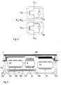
- Such a press pack moduleis described in the pending European patent application with the application number 01810539.5 described, and schematically in Fig. 1 shown. The figure is divided into two halves, on the left half of the module in the pre-assembled state and on the right half of the other half of the module in the assembled state in a stack of three modules is shown.
- the module with the three submodules 2 shownis pressed against an electrically and thermally well conductive base plate 12, which may be, for example, a traversed by a cooling liquid cooling plate.
- the second main terminals 4 of the submodulesare pressed into the interior of the module housing by a contact force exerted on the base and cover plates.
- the spring elementsare compressed, whereby an increased contact force acts on the electrodes of the semiconductor chips in the interior of the submodules.
- the insulating housingensures that the spring elements are not compressed too much, so that the contact force is not too large.
- a stack with press pack modulesreaches a length of several meters.
- complex precautionsare necessary. It is therefore desirable to increase the maximum blocking voltage per unit length in a stack in order to manage for a given voltage with fewer press pack modules.
- the power semiconductor module according to the inventioncomprises at least two submodules between two main electrical connections, which are arranged on mutually opposite, essentially parallel main surfaces of the module.
- the submoduleshave two main electrical connections, which are arranged on each one of two opposing, substantially parallel main surfaces of the submodules.
- the submoduleseach comprise at least one semiconductor chip which has two main electrodes, which are electrically conductively connected to the main terminals of the submodule.
- the submodulesare arranged side by side and pressed against the cover plate with one of the two main surfaces. At least two submodules are electrically connected in series.
- the reverse voltagecan be doubled or multiplied compared to conventional press pack modules.
- the overall height of the power semiconductor module according to the inventionincreases only slightly compared with conventional press-pack modules.
- the additional magnificationleads to an improved mechanical stability of the module, which is especially advantageous in long stacks.
- the first main connection of at least one first submoduleis electrically conductively connected to the cover plate.
- a first electrically insulating layeris arranged between the second main terminal of the at least one first submodule and the main surface of the module opposite the cover plate, and a second electrically insulating layer is arranged between the first main terminal of at least one second submodule and the cover plate.
- the second main connection of the at least one second submoduleis electrically conductively connected to the second main connection of the module.
- the second main connection of the at least one first submoduleis electrically conductively connected to the first main connection of the at least one second submodule via a connection.
- the submodulesare electrically connected in series, resulting in a double reverse voltage for the power semiconductor module with IGBT semiconductors.
- a first electrically insulating layeris arranged between the first main terminal of at least one first submodule and the main surface of the module opposite the cover plate.
- the first main connection of the at least one first submoduleis electrically conductively connected to the cover plate via a first connection.
- a second electrically insulating layeris arranged between the second main connection of the at least one first submodule and the cover plate and between the first main connection of at least one second submodule and the cover plate.
- the second main connection of the at least one second submoduleis electrically conductively connected to the second main connection of the module.
- the second main connection of the at least one first submoduleis electrically conductively connected to the first main connection of the at least one second submodule via the second connection.
- the submodulesare switched electrically antiserial with the same orientation in the module. This results in a turn-off four-quadrant power semiconductor module with IGBT semiconductors, which is used for example as an AC switch in matrix converter.
- the Fig. 2 and 3show two embodiments of the inventive power semiconductor module.
- the modulecomprises an electrically conductive cover plate 11, an electrically insulating housing 5, which is connected in a conclusive manner to the cover plate, and a plurality of submodules 21 and 22.
- the cover plate 11is made of an electrically and thermally highly conductive metal, such as copper or aluminum. It forms the first main electrical connection E 21 of the module, which is electrically connected, for example, in a stack to the main connection of an overlying module.
- the housing 5is made of an electrically insulating, mechanically and thermally loadable material, such as epoxy.
- the housingincludes side wall portions that carry the majority of the pressure applied to the module in a press pack stack, and a bottom portion.
- the cover plate and the bottom portion of the housingform two opposing, substantially parallel major surfaces of the module.
- openings 51are recessed into the housing, through which a second main electrical connection of the module C 22 is guided out of the housing.
- the submodulesusually include, as in Fig. 1 indicated, a plurality of semiconductor chips which are arranged with a first main electrode (anode, emitter) side by side on a base plate and electrically connected in parallel. Second main electrodes (cathode, collector) of the semiconductor chips are contacted by contact punches.
- the contact stampsare connected to a first main terminal 3 and the base plate is connected to a second main terminal 4.
- the main connectionscan be disc-shaped and held together by means of flanges.
- the contact stampincludes, for example, spring elements which press on the individual chips. Further connections (control / gate connections) of the semiconductor chips are led out of the submodule for contacting laterally or on one of the sides of the main connections 3 or 4.
- the two submodulesare pressed between the two main surfaces of the module, in particular between the cover plate 11 and a base plate, not shown, guided from below to the module base plate.
- the base platefor example, formed as a flowed through by a cooling liquid cooling plate, is electrically and thermally well conductive.
- control terminals G 21 and G 22are control terminals G 21 and G 22 as well as terminals E 21 and C 21 / E 22 which are connected to corresponding main terminals of the submodules.
- the first submodule 21with the first main terminal 3 directly to the cover plate 11 of the module and is connected to it electrically conductive.
- the first submodule 21lies on an insulating support plate 6 which consists essentially of a layer 61 of an electrically insulating and thermally highly conductive material.
- the insulating support plateadvantageously comprises a ceramic substrate, with a ceramic layer surrounded on both sides by copper layers. The copper layers provide good thermal contacts and contribute to the stability of the plate.
- the second submodule 22likewise rests against the cover plate 11 of the module with the first main connection 3, but is electrically insulated from it by a layer 62 of an electrically insulating and thermally highly conductive material.
- the second submodule 22is arranged in one of the openings 51 in the bottom region of the housing 5 that the second main terminal 4 when applying the module to the base, or cooling plate, the second main terminal of the module C 22 , or together with the insulating support plate 6 which forms the cover plate 11 opposite major surface of the module.
- the insulating support plate 6 and the second sub-module 22are movably arranged in the openings. If the module is placed on a base or cooling plate and subjected to a corresponding pressing force, insulating support plate 6 and the second sub-module 22 are pressed into the interior of the module housing and against the cover plate. The range of motion is limited by the insulating housing, in particular the wall areas. So that insulating support plate 6 and submodule 22 do not fall out of the module housing, if the module is not arranged on the base or cooling plate, securing means are provided in the region of the openings. For example, these may be stops attached to the housing, which limit the freedom of movement of the insulating support plate and the submodule accordingly.
- the two submodules of in Fig. 2 Dargestellen first embodiment of the inventive power semiconductor moduleare electrically connected to a series circuit.
- the submodulesare, for example, each equipped with one or more IGBTs and a parallel free-wheeling diode, so that the module in Fig. 4 shown circuit diagram results.
- the two main electrodes of the submoduleswhich are each separated by an insulating layer from the adjacent main surface of the module, the second main electrode 4 of the first submodule 21 and the first main electrode 3 of the second submodule 22, are electrically connected together.
- a first electrically conductive connecting layer 71is arranged on the insulating support plate 6, between the insulating layer 71 and the second main terminal 4 of the first submodule 21, a first electrically conductive connecting layer 71 is arranged.
- Theseare, for example, the above-mentioned copper layer of the ceramic substrate, or a further metal layer attached to this copper layer.
- the second main connection of the submodule 21is connected either to the connection layer 71 conclusively, for example by soldering or by an LTB (Low Temperature Bond) connection, or via a layer of thermal compound and corresponding contact pressure.
- a second electrically conductive connection layer 72is arranged between the insulating layer 62 and the main terminal 3 of the submodule.
- the two connecting layers 71 and 72are electrically conductively connected to one another via a connecting element 8.
- the connecting element 8is constructed, for example, analogously to the two submodules 21 and 22 and comprises a base plate and one or more contact punches with spring elements. In this way, the connecting element 8 as the submodules between the corresponding contact surfaces is compressible.
- the connecting element 8, which as a rule does not contain any electronic elements,can also be replaced by a conventional submodule with semiconductor chips or other electronic elements.
- the connecting element 8is arranged or fastened analogously to the first submodule on the insulating support plate.
- projections 63are provided of electrically insulating material. These act on the one hand with the stops on the housing parts 50 together, on the other hand, they prevent leakage currents or flashovers along the adjacent housing parts. In addition, together with positioning elements 64 arranged between the first submodule 8 and the connecting element 8, they ensure that the submodule 21 and the connecting element 8 are correctly positioned with respect to the insulating support plate 6 and the remaining module.
- Emitter pieceie in the region of the first main terminals 3, 21 and 22 are attached to the submodules control terminals. These are connected inside the submodules with corresponding control electrodes of the semiconductor chips. These control terminals G 21 and G 22 are led with connection lines from the housing of the module, where they together with the emitter terminal E 21 of the first submodule or the combined terminal C 21 / E 22 can be contacted to the collector terminal of the first submodule and the emitter terminal of the second submodule, which are also guided with connection lines from the housing.
- the currentflows in the on state from the second main terminal of the module, the collector terminal C 22 of the second submodule 22 through the second submodule via the emitter terminal E 22 of the second submodule, the second connection layer 72, the connecting element 8, the first connection layer 71 and the collector terminal C 21 of the first submodule 21 through the first submodule to the first main terminal of the module, the cover plate 11, and the emitter terminal C21 of the first submodule.
- the two submodulesare electrically connected to an anti-series circuit.
- the first submodule 21is connected to the cover plate or the first main connection of the module via the second main connection 4 and the first main connection 3 of the first submodule 3 is connected to the first main connection 3 of the second submodule 22.
- IGBT and parallel freewheeling diodethis results in the module in Fig. 5 illustrated circuit diagram.
- the first submodule 21is arranged the same in the second embodiment, but it is connected electrically reversed polarity.
- the first submodule 21also rests against the first main connection 3 on the cover plate 11 of the module, it is not electrically conductively connected to it.
- an insulating layer 62is arranged between the main terminal of the submodule and the cover plate. It is the extended insulating layer 62 which is arranged between the second sub-module 22 and the cover plate 11.
- the two first main terminals 3 of the two submodulesare electrically conductively connected to one another via the connection layer 72.
- the connecting layeris arranged between the main terminals and the insulating layer 62.
- the second main terminal 4 of the first submoduleis electrically connected to the cover plate 11 via the connecting layer 71 and the connecting element 8 arranged on the insulating support plate 6.
- the connecting element 8is guided through a central opening in the insulating and connecting layer 62 and 72 to the cover plate 11.
- the connecting layer 72has a greater thickness in the region of the first main terminal 3 of the second submodule 22 than the first main terminal of the first, by the thickness of the insulating support plate 6, including any connecting layer 71 arranged thereon Submodule 21.
- the collector-emitter currentthus flows in each case from the two main terminals of the module C 21 and C 22 either through the connecting element 8, via the connecting layer 71 and the second main terminal 4 of the first submodule 21 and through the first submodule 21 to the first main terminal 3 of the emitter Terminal E 21 of, or through the second submodule 22 to the corresponding emitter terminal E 22nd
- the emitter terminals E 21 and E 22, which are connected to one another in an electrically conductive manner by the connection layer 72,are led out of the module housing for external contacting together with the corresponding control terminals G 21 and G 22 via connection lines. Instead of both, only one of the emitter terminals can be guided out of the housing.
- the two led out of the housing connections of the two submodulesare each arranged on opposite sides of the module.
- all connectionsare arranged on one side of the module, whereby the external contacting of the module via these connections is simplified.
- the connection lines inside the module housingare guided on one side accordingly.
- connection lines together with the second connection layer 72 and the cover plate 11are encapsulated with an electrically insulating material to form a cover unit 10.
- the electrically insulating materialis advantageously thermally highly conductive, temperature-resistant up to 160 ° C, pressure-resistant up to 30 bar, creep-resistant, void-free pourable and has a copper adapted coefficient of expansion.
- a material which combines these propertiesis, for example, epoxy.
- the epoxyis either cast in a corresponding form around the electrically conductive parts, or applied by spraying.
- FIG Fig. 6How the individual elements of the power semiconductor module according to the invention are assembled during mounting is shown in FIG Fig. 6 seen.
- the insulating support plate 6is inserted in a first assembly step. By stops on the housing parts 50 in the region of the openings 51, the insulating support plate 6 is held. On the insulating plate 6, the insulating ends 63 are mounted in the edge region which, as can be seen from the figure, cooperate with the corresponding stops on the housing parts 50.
- the submodules 21 and 22 and the connecting element 8are guided into the housing.
- the first submodule 21 and the connecting element 8are fastened on the insulating support plate 8, while the second submodule 22 is inserted into the opening 51 provided for this purpose.
- the second submodule 22is prevented from falling out by corresponding stops on the housing parts 50.
- positioning elements 64are arranged on the insulating support plate 6.
- the Isolierab say 63also serve the positioning.
- the first sub-module 21 and connecting member 8are mounted on the insulating support plate 6 and possibly attached thereto before the insulating support plate is placed in the housing.
- the cover unit 10is placed on the housing. Thanks to the precise positioning of the submodules, the interconnection layers and connection lines integrated in the cover unit are combined with the corresponding contact connections of the submodules.
- the contact pressure on the housing coverprovides the necessary contact force for the pressure-contacted contact connections of the submodules. To improve the electrical and thermal transition, can be applied between the pressure-contacted contact surfaces corresponding thermal paste.
- the aforementioned series or antiseries circuit of semiconductor chipscan also be achieved by corresponding reversal (turning) of the submodules, or of the semiconductor chips arranged in the submodule.
- the anti-series circuit according to the circuit Fig. 5realize.
- series connectionalso includes the series connection of two components with opposite polarity (anti-series connection).
Landscapes
- Engineering & Computer Science (AREA)
- Microelectronics & Electronic Packaging (AREA)
- Power Engineering (AREA)
- Computer Hardware Design (AREA)
- Physics & Mathematics (AREA)
- Condensed Matter Physics & Semiconductors (AREA)
- General Physics & Mathematics (AREA)
- Inverter Devices (AREA)
- Cooling Or The Like Of Semiconductors Or Solid State Devices (AREA)
Description
Translated fromGermanDie Erfindung bezieht sich auf das Gebiet der Leistungselektronik. Sie betrifft ein Leistungshalbleiter-Modul nach dem Oberbegriff des Patentanspruchs 1.The invention relates to the field of power electronics. It relates to a power semiconductor module according to the preamble of
Im Hochleistungsbereich werden Leistungshalbleiter-Module in der Druckkontakttechnik (Press Pack Module) gefertigt. Diese Press Pack Module werden als Hochleistungsschalter im Hochspannungsbereich bis 1'000 kV für Ströme bis zu mehreren kA eingesetzt. Da ein Insulated Gate Bipolar Transistor (IGBT), wie er heute in einem Press Pack Modul verwendet wird, lediglich eine Spannung von rund einigen kV sperren kann, werden für einen Hochspannungsschalter mehrere Press Pack Module in mindestens einem Stapel (Stack) in Serie geschaltet. Der Stack mit bis mehreren Dutzend Press Pack Modulen wird mit einer Kraft von rund 100 kN zusammengepresst.In the high-power range, power semiconductor modules are manufactured using pressure contact technology (Press Pack Module). These press pack modules are used as high-power switches in the high voltage range up to 1'000 kV for currents up to several kA. Since an insulated gate bipolar transistor (IGBT), as used in a press pack module today, can only block a voltage of about a few kV, several press pack modules are connected in series in at least one stack for a high voltage switch. The stack with up to several dozen Press Pack modules is compressed with a force of around 100 kN.
Ein herkömmliches Press Pack Modul, wie es beispielsweise in
Die einzelnen Halbleiterchips des Press Pack Moduls werden vielfach gruppiert und in vorfabrizierbaren Einheiten, sogenannte Submodule, zusammengefasst. Dabei sind die Halbleiterchips zueinander parallel geschaltet, beispielsweise ein IGBT- und ein Dioden-Chip gemeinsam in einem Submodul.The individual semiconductor chips of the press pack module are grouped in many groups and combined in prefabricatable units, so-called submodules. Here are the Semiconductor chips connected in parallel to each other, for example, an IGBT and a diode chip together in a submodule.
Ein solches Press Pack Modul ist in der anhängigen europäischen Patentanmeldung mit der Anmeldenummer
Das Modul mit den drei dargestellten Submodulen 2 wird dabei gegen eine elektrisch und thermisch gut leitende Grundplatte 12 gepresst, die beispielsweise eine von einer Kühlflüssigkeit durchflossene Kühlplatte sein kann.The module with the three
Bereits im vormontierten Zustand sind die von oben in das Isoliergehäuse 5 eingebrachten Submodule 2 mit einer Federspannung beaufschlagt und werden gegen die fest mit dem Isoliergehäuse verbundene Deckelplatte 11 gepresst. Die Federspannung wird von Federelementen in den einzelnen Submodulen erzeugt und auf die ersten Hauptanschlüsse 3 übertragen. Die zweiten Hauptanschlüsse 4 ragen unten aus dem Isoliergehäuse 5 hervor um einen sicheren Kontakt zur Grundplatte 12 zu gewährleisten.Already in the preassembled state introduced from above into the insulating 5
Im montierten Zustand sind die zweiten Hauptanschlüsse 4 der Submodule durch eine auf die Grund- und die Deckelplatte ausgeübte Anpresskraft ins Innere des Modulgehäuses gedrückt. Dabei werden die Federelemente komprimiert, wodurch ein erhöhte Kontaktkraft auf die Elektroden der Halbleiterchips im Innern der Submodule wirkt. Das Isoliergehäuse sorgt dabei dafür, dass die Federelemente nicht zu stark komprimiert werden, damit die Kontaktkraft nicht zu gross wird.In the mounted state, the second
Ein Stack mit Press Pack Modulen erreicht eine Länge von mehreren Metern. Um den oben erwähnten Druck über eine solche Länge ausüben zu können, sind aufwendige Vorkehrungen notwendig. Es ist daher erstrebenswert, die maximale Sperrspannung pro Längeneinheit in einem Stack zu erhöhen, um für eine gegebene Spannung mit weniger Press Pack Modulen auszukommen.A stack with press pack modules reaches a length of several meters. In order to exercise the above-mentioned pressure over such a length, complex precautions are necessary. It is therefore desirable to increase the maximum blocking voltage per unit length in a stack in order to manage for a given voltage with fewer press pack modules.
Durch eine Erhöhung der Sperrspannung einzelner Press Pack Module könnten die Höhe des Stacks und die damit verbundenen Kosten reduziert werden. Leider ist die oben erwähnte maximale Sperrspannung der Leistungshalbleiterchips mit der heutigen Technologie kaum zu überbieten.By increasing the blocking voltage of individual Press Pack modules, the height of the stack and the associated costs could be reduced. Unfortunately, the above-mentioned maximum reverse voltage of power semiconductor chips with today's technology is hard to beat.
Es ist daher die Aufgabe der vorliegenden Erfindung, ein Leistungshalbleiter-Modul der eingangs genannten Art zu schaffen, welches eine höhere Sperrspannung pro Bauhöhe aufweist.It is therefore an object of the present invention to provide a power semiconductor module of the type mentioned, which has a higher reverse voltage per height.
Diese Aufgabe wird erfindungsgemäss mit einem Leistungshalbleiter-Modul mit den Merkmalen des Patentanspruchs 1 gelöst.This object is achieved according to the invention with a power semiconductor module having the features of
Das erfindungsgemässe Leistungshalbleiter-Modul umfasst zwischen zwei elektrischen Hauptanschlüssen, welche auf einander gegenüberliegenden, im wesentlichen parallelen Hauptoberflächen des Moduls angeordnet sind, mindestens zwei Submodule. Die Submodule weisen zwei elektrische Hauptanschlüsse auf, welche auf je einer von zwei einander gegenüberliegenden, im wesentlichen parallelen Hauptoberflächen der Submodule angeordnet sind. Die Submodule umfassen je mindestens einen Halbleiterchip, welcher zwei Hauptelektroden aufweist, welche mit den Hauptanschlüssen des Submoduls elektrisch leitend verbunden sind. Die Submodule sind nebeneinander angeordnet und mit einer der beiden Hauptoberflächen an die Deckelplatte angepresst. Mindestens zwei Submodule sind elektrisch in Serie geschaltet.The power semiconductor module according to the invention comprises at least two submodules between two main electrical connections, which are arranged on mutually opposite, essentially parallel main surfaces of the module. The submodules have two main electrical connections, which are arranged on each one of two opposing, substantially parallel main surfaces of the submodules. The submodules each comprise at least one semiconductor chip which has two main electrodes, which are electrically conductively connected to the main terminals of the submodule. The submodules are arranged side by side and pressed against the cover plate with one of the two main surfaces. At least two submodules are electrically connected in series.
Durch die Serienschaltung von zwei oder mehreren nebeneinander angeordneten Submodulen kann im Vergleich zu herkömmlichen Press Pack Modulen die Sperrspannung verdoppelt oder vervielfacht werden.By series connection of two or more juxtaposed submodules, the reverse voltage can be doubled or multiplied compared to conventional press pack modules.
Dadurch reduziert sich die Länge und die Kosten eines Stacks da für die gleichen Sperrspannungen weniger Komponenten, insbesondere weniger Kühlelemente, gebraucht werden,.This reduces the length and the cost of a stack as fewer components, in particular fewer cooling elements, are needed for the same blocking voltages.
Die Bauhöhe des erfindungsgemässen Leistungshalbleiter-Moduls vergrössert sich gegenüber herkömmlichen Press Pack Modulen nur geringfügig. Die zusätzliche Vergrösserung führt jedoch zu einer verbesserten mechanischen Stabilität des Moduls, was insbesondere in langen Stacks besonders vorteilhaft zum tragen kommt.The overall height of the power semiconductor module according to the invention increases only slightly compared with conventional press-pack modules. However, the additional magnification leads to an improved mechanical stability of the module, which is especially advantageous in long stacks.
Weiter ist es möglich, für gleichbleibende oder grössere Sperrspannungen im Vergleich zu herkömmlichen Press Pack Modulen günstigere Halbleiterchips mit geringerer Sperrspannung zu verwenden. Da solche Halbleiterchips mit der halben Sperrspannung zusammen weniger Verluste produzieren als ein einzelner Halbleiterchip mit der vollen Sperrspannung, können in herkömmlichen Stacks bei gleichbleibenden Abmessungen mit den erfindungsgemässen Leistungshalbleiter-Modulen auch die Verluste reduziert werden.Furthermore, it is possible to use cheaper semiconductor chips with a lower reverse voltage for constant or larger reverse voltages compared to conventional press-pack modules. Since such semiconductor chips together with half the blocking voltage produce less losses than a single semiconductor chip with the full reverse voltage, can in conventional stacks with constant dimensions With the power semiconductor modules according to the invention, the losses are also reduced.
In einer ersten Ausführungsform des Leistungshalbleiter-Moduls ist der erste Hauptanschluss mindestens eines ersten Submoduls mit der Deckelplatte elektrisch leitend verbunden. Zwischen dem zweiten Hauptanschluss des mindestens einen ersten Submoduls und der der Deckelplatte gegenüberliegenden Hauptoberfläche des Moduls ist eine erste elektrisch isolierende Schicht und zwischen dem ersten Hauptanschluss mindestens eines zweiten Submoduls und der Deckelplatte ist eine zweite elektrisch isolierende Schicht angeordnet. Der zweite Hauptanschluss des mindestens einen zweiten Submoduls ist mit dem zweiten Hauptanschluss des Moduls elektrisch leitend verbunden. Der zweite Hauptanschluss des mindestens einen ersten Submoduls ist mit dem ersten Hauptanschluss des mindestens einen zweiten Submoduls über eine Verbindung elektrisch leitend verbunden ist.In a first embodiment of the power semiconductor module, the first main connection of at least one first submodule is electrically conductively connected to the cover plate. A first electrically insulating layer is arranged between the second main terminal of the at least one first submodule and the main surface of the module opposite the cover plate, and a second electrically insulating layer is arranged between the first main terminal of at least one second submodule and the cover plate. The second main connection of the at least one second submodule is electrically conductively connected to the second main connection of the module. The second main connection of the at least one first submodule is electrically conductively connected to the first main connection of the at least one second submodule via a connection.
Die Submodule sind elektrisch in Serie geschaltet, wodurch sich für das Leistungshalbleiter-Modul mit IGBT-Halbleitern eine doppelte Sperrspannung ergibt.The submodules are electrically connected in series, resulting in a double reverse voltage for the power semiconductor module with IGBT semiconductors.
In einer zweiten Ausführungsform des Leistungshalbleiter-Moduls ist zwischen dem ersten Hauptanschluss mindestens eines ersten Submoduls und der der Deckelplatte gegenüberliegenden Hauptoberfläche des Moduls eine erste elektrisch isolierende Schicht angeordnet ist. Der erste Hauptanschluss des mindestens einen ersten Submoduls ist über eine erste Verbindung mit der Deckelplatte elektrisch leitend verbunden. Zwischen dem zweiten Hauptanschluss des mindestens einen ersten Submoduls und der Deckelplatte sowie zwischen dem ersten Hauptanschluss mindestens eines zweiten Submoduls und der Deckelplatte ist eine zweite elektrisch isolierende Schicht angeordnet. Der zweite Hauptanschluss des mindestens einen zweiten Submoduls ist mit dem zweiten Hauptanschluss des Moduls elektrisch leitend verbunden. Der zweite Hauptanschluss des mindestens einen ersten Submoduls ist mit dem ersten Hauptanschluss des mindestens einen zweiten Submoduls über zweite Verbindung elektrisch leitend verbunden.In a second embodiment of the power semiconductor module, a first electrically insulating layer is arranged between the first main terminal of at least one first submodule and the main surface of the module opposite the cover plate. The first main connection of the at least one first submodule is electrically conductively connected to the cover plate via a first connection. A second electrically insulating layer is arranged between the second main connection of the at least one first submodule and the cover plate and between the first main connection of at least one second submodule and the cover plate. The second main connection of the at least one second submodule is electrically conductively connected to the second main connection of the module. The second main connection of the at least one first submodule is electrically conductively connected to the first main connection of the at least one second submodule via the second connection.
Die Submodule sind bei gleicher Ausrichtung im Modul elektrisch antiseriel geschaltet. Dadurch ergibt sich mit IGBT-Halbleitern ein abschaltbares Vier-Quadranten-Leistungshalbleiter-Modul, welches beispielsweise als Wechselstrom-Schalter in Matrixstromrichter eingesetzt wird.The submodules are switched electrically antiserial with the same orientation in the module. This results in a turn-off four-quadrant power semiconductor module with IGBT semiconductors, which is used for example as an AC switch in matrix converter.
Weitere Ausführungsbeispiele und Vorteile ergeben sich aus den entsprechenden abhängigen Ansprüchen.Further embodiments and advantages emerge from the corresponding dependent claims.
Nachfolgend wird die Erfindung anhand von Ausführungsbeispielen im Zusammenhang mit den Zeichnungen näher erläutert. Es zeigen:
- Fig. 1
- ein Schnitt durch ein Leistungshalbleiter-Modul nach dem Stand der Technik, im vormontierten (linke Bildhälfte) und im montierten Zustand (rechte Bildhälfte),
- Fig. 2
- eine Schnitt durch eine erste Ausführungsform eines erfindungsgemässen Leistungshalbleiter-Moduls mit zwei seriell geschalteten Submodulen, und
- Fig. 3
- eine Schnitt durch das Leistungshalbleiter-Modul gemäss
Fig. 2 mit zwei anti-seriell geschalteten Submodulen, - Fig. 4
- ein Schema des Leistungshalbleiter-Muduls gemäss
Fig. 2 , - Fig. 5
- ein Schema des Leistungshalbleiter-Muduls gemäss
Fig. 3 , und - Fig. 6
- ein Schnitt durch das Leistungshalbleiter-Modul gemäss
Fig. 3 beim Montieren.
- Fig. 1
- a section through a power semiconductor module according to the prior art, in the pre-assembled (left half) and in the assembled state (right half),
- Fig. 2
- a section through a first embodiment of a power semiconductor module according to the invention with two series-connected submodules, and
- Fig. 3
- a section through the power semiconductor module according to
Fig. 2 with two anti-serial submodules, - Fig. 4
- a diagram of the power semiconductor Muduls according
Fig. 2 . - Fig. 5
- a diagram of the power semiconductor Muduls according
Fig. 3 , and - Fig. 6
- a section through the power semiconductor module according to
Fig. 3 when mounting.
Die in den Zeichnungen verwendeten Bezugszeichen und deren Bedeutung sind in der Bezeichnungsliste zusammengefasst aufgelistet. Grundsätzlich sind in den Figuren gleiche Teile mit gleichen Bezugszeichen versehen.The reference numbers used in the drawings and their meaning are listed in the list of names. Basically, the same parts are provided with the same reference numerals in the figures.
Die
Die Deckelplatte 11 ist aus einem elektrisch und thermisch gut leitenden Metall, beispielsweise Kupfer oder Aluminium, gefertigt. Sie bildet den ersten elektrischen Hauptanschluss E21 des Moduls, welcher beispielsweise in einem Stack mit dem Hauptanschluss eines darüberliegenden Moduls elektrisch verbunden ist.The
Das Gehäuse 5 ist aus einem elektrisch isolierenden, mechanisch und thermisch belastbaren Material, beispielsweise Epoxy, gefertigt. Das Gehäuse umfasst seitliche Wandbereiche, welche den Hauptanteil der in einem Press Pack Stack auf das Modul ausgeübten Anpresskraft tragen, sowie einen Bodenbereich. Die Deckelplatte und der Bodenbereich des Gehäuses bilden zwei gegenüberliegende, im wesentlichen parallele Hauptoberflächen des Moduls. Im Bodenbereich sind Öffnungen 51 in das Gehäuse eingelassen, durch die ein zweiter elektrischer Hauptanschluss des Moduls C22 aus dem Gehäuse geführt ist.The
Im Innern des Moduls sind zwei an sich bekannte Leistungshalbleiter-Submodule 21 und 22 nebeneinander angeordnet. Die Submodule umfassen in der Regel, wie in
Die beiden Submodule sind zwischen den beiden Hauptoberflächen des Moduls, insbesondere zwischen der Deckelplatte 11 und einer nicht dargestellten, von unten an das Modul geführten Grundplatte, eingepresst. Die Grundplatte, beispielsweise als eine von einer Kühlflüssigkeit durchströmte Kühlplatte ausgebildet, ist elektrisch und thermisch gut leitend.The two submodules are pressed between the two main surfaces of the module, in particular between the
Das Modul weist seitlich aus dem Modulgehäuse geführte Anschlüsse auf, je nach Art der Leistungshalbleiter sind dies Steueranschlüsse G21 und G22 sowie Anschlüsse E21 und C21/E22 welche mit entsprechenden Hauptanschlüssen der Submodule verbunden sind.Depending on the type of power semiconductor, these are control terminals G21 and G22 as well as terminals E21 and C21 / E22 which are connected to corresponding main terminals of the submodules.
In der ersten Ausführungsform des erfindungsgemässen Leistungshalbleiter-Moduls nach
Das zweite Submodul 22 liegt mit dem ersten Hauptanschluss 3 ebenfalls an der Deckelplatte 11 des Moduls an, ist von der jedoch durch eine Schicht 62 aus einem elektrisch isolierenden und thermisch gut leitenden Material elektrisch isoliert. Mit dem zweiten Hauptanschluss 4 ist das zweite Submoduls 22 derart in einer der Öffnungen 51 im Bodenbereich des Gehäuses 5 angeordnet, dass der zweite Hauptanschluss 4 beim Aufbringen des Moduls auf die Grund-, bzw. Kühlplatte den zweiten Hauptanschluss des Moduls C22, bzw. zusammen mit der Isolierträgerplatte 6 die der Deckelplatte 11 gegenüberliegende Hauptoberfläche des Moduls bildet.The
Die Isolierträgerplatte 6 und das zweite Submodul 22 sind in den Öffnungen bewegbar angeordnet. Wird das Modul auf eine Grund- bzw. Kühlplatte gebracht und entsprechend mit einer Anpresskraft beaufschlagt, werden Isolierträgerplatte 6 und das zweite Submodul 22 ins Innere des Modulgehäuses und gegen die Deckelplatte gedrückt. Der Bewegungsbereich wird durch das Isoliergehäuse, insbesondere die Wandbereiche, begrenzt. Damit Isolierträgerplatte 6 und Submodul 22 nicht aus dem Modulgehäuse fallen, wenn das Modul nicht auf der Grund- bzw. Kühlplatte angeordnet ist, sind im Bereich der Öffnungen Sicherungsmittel vorgesehen. Beispielsweise können dies an dem Gehäuse angebrachte Anschläge sein, welche die Bewegungsfreiheit der Isolierträgerplatte und des Submoduls entsprechend begrenzen.The insulating
Die beiden Submodule der in
Die beiden Hauptelektroden der Submodule, welche jeweils durch eine Isolierschicht von der angrenzenden Hauptoberfläche des Moduls getrennt sind, die zweite Hauptelektrode 4 des ersten Submoduls 21 sowie die erste Hauptelektrode 3 des zweiten Submoduls 22 also, sind elektrisch miteinander verbunden.The two main electrodes of the submodules, which are each separated by an insulating layer from the adjacent main surface of the module, the second
Auf der Isolierträgerplatte 6, zwischen der Isolierschicht 71 und dem zweiten Hauptanschluss 4 des ersten Submoduls 21 ist eine erste elektrisch leitende Verbindungsschicht 71 angeordnet. Dabei handelt es sich beispielsweise um die oben erwähnte Kupferschicht des Keramiksubstrats, oder eine auf dieser Kupferschicht angebrachte weitere Metallschicht. Der zweite Hauptanschluss des Submoduls 21 ist entweder mit der Verbindungsschicht 71 schlüssig, beispielsweise durch Auflöten oder durch eine LTB (Low Temperature Bond)-Verbindung, oder über eine Schicht Wärmeleitpaste und entsprechenden Anpressdruck verbunden.On the insulating
Auf der gegenüberliegenden Seite, im Bereich des ersten Hauptanschlusses 3 des zweiten Submoduls 22 ist zwischen der Isolierschicht 62 und dem Hauptanschluss 3 des Submoduls eine zweite elektrisch leitende Verbindungsschicht 72 angeordnet.On the opposite side, in the region of the first
Die beiden Verbindungsschichten 71 und 72 sind über ein Verbindungselement 8 miteinander elektrisch leitend verbunden. Das Verbindungselement 8 ist beispielsweise analog den beiden Submodulen 21 und 22 aufgebaut und umfasst eine Grundplatte sowie einen oder mehrere Kontaktstempel mit Federelementen. Auf diese Weise ist das Verbindungselement 8 wie die Submodule zwischen den entsprechenden Kontaktflächen komprimierbar. Das in der Regel keine elektronische Elemente enthaltende Verbindungselement 8 kann auch durch ein herkömmliches Submodul mit Halbleiterchips oder anderen elektronischen Elementen ersetzt werden. Das Verbindungselement 8 ist analog dem ersten Submodul auf der Isolierträgerplatte angeordnet bzw. befestigt.The two connecting
Im Randbereich der Isolierträgerplatte 6 sind Vorsprünge 63 aus elektrisch isolierendem Material vorgesehen. Diese wirken einerseits mit den Anschlägen an den Gehäuseteilen 50 zusammen, andererseits verhindern sie Kriechströme oder Überschläge entlang den angrenzenden Gehäuseteilen. Zudem sorgen sie zusammen mit zwischen dem erstem Submodul 8 und dem Verbindungselement 8 angeordneten Positionierungselementen 64 dafür, dass Submodul 21 und Verbindungselement 8 bezüglich der Isolierträgerplatte 6 sowie dem restlichen Modul richtig positioniert sind.In the edge region of the insulating
Emitterseitig, also im Bereich der ersten Hauptanschlüsse 3, sind an den Submodulen 21 und 22 Steueranschlüsse angebracht. Diese sind im Innern der Submodule mit entsprechenden Steuerelektroden der Halbleiterchips verbunden. Diese Steueranschlüsse G21 und G22 werden mit Anschlussleitungen aus dem Gehäuse des Moduls geführt, wo sie zusammen mit dem Emitteranschluss E21 des ersten Submoduls bzw. dem kombinierten Anschluss C21/ E22 auf den Kollektoranschluss des ersten Submoduls und den Emitteranschluss des zweiten Submoduls, welche ebenfalls mit Anschlussleitungen aus dem Gehäuse geführt sind, kontaktiert werden können.Emitterseitig, ie in the region of the first
Der Strom fliesst im eingeschalteten Zustand vom zweiten Hauptanschluss des Moduls, dem Kollektoranschluss C22 des zweiten Submoduls 22 durch das zweite Submodul über den Emitteranschluss E22 des zweiten Submoduls, die zweite Verbindungsschicht 72, das Verbindungselement 8, die erste Verbindungsschicht 71 und den Kollektoranschluss C21 des ersten Submoduls 21 durch das erste Submodul zum ersten Hauptanschluss des Moduls, der Deckelplatte 11, bzw. dem Emitteranschluss C21 des ersten Submoduls.The current flows in the on state from the second main terminal of the module, the collector terminal C22 of the
Im sperrenden Zustand fällt jeweils die halbe Sperrspannung über je einem der beiden Submodule an.In the blocking state, half the blocking voltage is applied to one of the two submodules.
In der zweiten Ausführungsform des erfindungsgemässen Leistungshalbleiter-Moduls nach
Während das zweite Submodul 22 unverändert gegenüber der ersten Ausführungsform angeordnet und elektrisch angeschlossen ist, ist das erste Submodul 21 in der zweiten Ausführugnsform zwar gleich angeordnet, jedoch ist es elektrisch umgekehrt gepolt angeschlossen.While the
Das erste Submodul 21 liegt zwar auch mit dem ersten Hauptanschluss 3 an der Deckelplatte 11 des Moduls an, ist jedoch nicht elektrisch leitend mit ihr verbunden. Zwischen dem Hauptanschluss des Submoduls und der Deckelplatte ist eine Isolierschicht 62 angeordnet. Es handelt sich dabei um die verlängerte Isolierschicht 62 welche zwischen dem zweiten Submodul 22 und der Deckelplatte 11 angeordnet ist. Die beiden ersten Hauptanschlüsse 3 der beiden Submodule sind über die Verbindungsschicht 72 elektrisch leitend miteinander verbunden. Die Verbindungsschicht ist dabei zwischen den Hauptanschlüssen und der Isolierschicht 62 angeordnet.Although the
Mit dem zweiten Hauptanschluss 4 liegt das erste Submodul 21 wiederum auf der isolierträgerplatte 6. Der zweite Hauptanschluss 4 des ersten Submoduls ist über die auf der Isolierträgerplatte 6 angeordnete Verbindungsschicht 71 und das Verbindungselement 8 elektrisch mit der Deckelplatte 11 verbunden. In der dargestellten, vorteilhaften Ausführungform ist das Verbindungselement 8 durch eine zentrale Öffnung in der Isolier- und Verbindungsschicht 62 und 72 zur Deckelplatte 11 geführt. The second
Da beide Submodule 21 und 22 gleiche Bauhöhe aufweisen, weist die Verbindungsschicht 72 im Bereich des ersten Hauptanschlusses 3 des zweiten Submoduls 22 eine um die Dicke der Isolierträgerplatte 6, inklusive allfällig darauf angeordneter Verbindungsschicht 71, grössere Dicke auf als im Bereich des ersten Hauptanschlusses des ersten Submoduls 21.Since both
Der Kollektor-Emitter-Strom fliesst somit jeweils von den beiden Hauptanschlüssen des Moduls C21 und C22 entweder durch das Verbindungselement 8, über die Verbindungsschicht 71 und den zweiten Hauptanschluss 4 des ersten Submoduls 21 und durch das erste Submodul 21 zum ersten Hauptanschluss 3der Emitter-Anschluss E21 des, oder durch das zweite Submodul 22 zum entsprechenden Emitter-Anschluss E22. Die durch die Verbindungsschicht 72 miteinander elektrisch leitend verbundenen Emitter-Anschlüsse E21 und E22 sind zum externen Kontaktieren zusammen mit den entsprechenden Steueranschlüssen G21 und G22 über Anschlussleitungen aus dem Modulgehäuse geführt. Anstelle von beiden, kann auch nur einer der Emitteranschlüsse aus dem Gehäuse geführt sein.The collector-emitter current thus flows in each case from the two main terminals of the module C21 and C22 either through the connecting
In den Darstellungen gemäss
In einer ganz besonders vorteilhaften Ausführungsform des erfindungsgemässen Leistungshalbleiter-Moduls sind die Anschlussleitungen zusammen mit der zweiten Verbindungsschicht 72 und der Deckelplatte 11 mit einem elektrisch isolierenden Material zu einer Deckeleinheit 10 vergossen. Das elektrisch isolierende Material ist vorteilhafterweise thermisch gut leitend, temperaturbeständig bis zu 160°C, druckbeständig bis zu 30 bar, kriechbeständig, lunkernfrei vergiessbar und weist einen an Kupfer angepassten Ausdehnungskoeffizienten aus. Ein Material welches diese Eigenschaften vereint ist beispielsweise Epoxy. Zur Herstellung der Deckeleinheit wird das Epoxy entweder in einer entsprechenden Form um die elektrisch leitenden Teile vergossen, oder durch Sprayen aufgebracht.In a particularly advantageous embodiment of the power semiconductor module according to the invention, the connection lines together with the
Wie die einzelnen Elemente des erfindungsgemässen Leistungshalbleiter-Moduls beim Montieren zusammengebaut werden, ist anhand der Darstellung in
In das mit den Öffnungen 51 versehene Gehäuse wird in einem ersten Montageschritt die Isolierträgerplatte 6 eingelegt. Durch Anschläge an den Gehäuseteilen 50 im Bereich der Öffnungen 51 wird die Isolierträgerplatte 6 gehalten. An der Isolierplatte 6 sind im Randbereich die Isolierabschlüsse 63 angebracht welche wie aus der Figur ersichtlich, mit den entsprechenden Anschlägen an den Gehäuseteilen 50 zusammenwirken.In the
In einem nächsten Montageschritt werden die Submodule 21 und 22 sowie das Verbindungselement 8 in das Gehäuse geführt. Das erste Submodul 21 und das Verbindungselement 8 werden auf der Isolierträgerplatte 8 befestigt, während das zweite Submodul 22 in die dafür vorgesehene Öffnung 51 eingelegt wird. Auch das zweite Submodul 22 wird durch entsprechende Anschläge an den Gehäuseteilen 50 am Herausfallen gehindert. Zur genauen Positionierung des ersten Submoduls 21 und des Verbindungselements 8 auf der Isolierträgerplatte 8 sind Positionierelemente 64 auf der Isolierträgerplatte 6 angeordnet. Die Isolierabschlüsse 63 dienen ebenfalls der Positionierung.In a next assembly step, the
Alternativ werden erstes Submodul 21 und Verbindungselement 8 auf der Isolierträgerplatte 6 angebracht und allenfalls daran befestigt, bevor die Isolierträgerplatte in das Gehäuse gelegt wird.Alternatively, the first sub-module 21 and connecting
In einem weiteren Montageschritt wird die Deckeleinheit 10 auf das Gehäuse aufgesetzt. Die in der Deckeleinheit integrierten Verbindungsschichten und Anschlussleitungen werden dank der genauen Positionierung der Submodule mit den entsprechenden Kontaktanschlüssen der Submodule zusammengeführt. Die Anpresskraft auf den Gehäusedeckel sorgt für die notwendige Kontaktkraft für die druckkontaktierten Kontaktanschlüsse der Submodule. Zum Verbessern des elektrischen und thermischen Übergangs, kann zwischen den druckkontatktierten Kontaktflächen entsprechende Wärmeleitpaste aufgetragen werden.In a further assembly step, the
Die erwähnte Serien- bzw. Antiserienschaltung von Halbleiterchips kann auch durch entsprechendes Umkehren (Wenden) der Submodule, bzw. der im Submodul angeordneten Halbleiterchips erreicht werden. Beispielsweise lässt sich durch ein gewendetes erstes Submodul (Flip-Submodul) in der oben erwähnten ersten Ausführungsform die Antiserienschaltung ensprechend der Schaltung nach
Im Sinne der Erfindung umfasst der allgemeine Begriff der Serienschaltung auch das Hintereinanderschalten zweier Komponenten mit entgegengesetzter Polarität (Anti-Serienschaltung).For the purposes of the invention, the general concept of series connection also includes the series connection of two components with opposite polarity (anti-series connection).
- 11
- Leistungshalbleiter-ModulPower semiconductor module
- 1010
- Deckeleinheitcover unit
- 1111
- Deckelplattecover plate
- 2, 21, 222, 21, 22
- Submodulsubmodule
- 3, 43, 4
- Hauptanschlüssemain lines
- 5, 505, 50
- Isoliergehäuseinsulating
- 51, 5251, 52
- Öffnungenopenings
- 66
- IsolierträgerplatteIsolierträgerplatte
- 61, 6261, 62
- Isolierschichteninsulating
- 6363
- IsolierabschlüsseIsolierabschlüsse
- 6464
- Positionierungselementpositioner
- 71, 7271, 72
- VerbindungsschichtenTie layers
- 88th
- Verbindungselementconnecting element
- C, C21, C22C, C21 , C22
- Kollektor-AnschlussCollector terminal
- E, E21, E22E, E21 , E22
- Emitter-AnschlussEmitter terminal
- G, G21, G22G, G21 , G22
- Gate-AnschlussGate terminal
Claims (15)
- Power semiconductor module having- two main electrical connections which are arranged on mutually opposite, essentially parallel, main surfaces of the module, with a first of the two main connections of the power semi conductor module being in the form of an electrically conductive covering plate (11),- an electrically insulating housing (5) which is connected to the covering plate (11) and is arranged between the two main connections, in which housing (5) at least one opening (51) is incorporated in the region of the main surface of the module which is opposite the covering plate (11), and- at least two submodules (2, 21, 22), with the submodules- having in each case two main electrical connections (3, 4) which are arranged on in each case one of two mutually opposite, essentially parallel, main surfaces of the submodules,- comprising in each case at least one semiconductor chip, which has two main electrodes which are electrically conductively connected to the main connections (3, 4) of the submodule, and- being arranged alongside one another,and- at least two submodules (21, 22) being electrically connected in series or back-to-back in series, and- the submodules (21, 22) being arranged to be movable in the openings (51) of the housing in such a way that the submodules (21, 22) can be pressed with in each case one of the two main surfaces against the covering plate (11) by a contact force that can be applied to them.
- Power semiconductor module according to Claim 1,characterized in that- the series-connected submodules (21, 22) are electrically conductively connected to one another via in each case one main connection (3, 4) and one connection (71, 72, 8), andin that- an electrically insulating layer (61, 62) is arranged between the main connections (3, 4), which are connected to one another, of the submodules (21, 22) and of the respective main surface of the module.
- Power semiconductor module according to Claim 2,characterized in that- a first main connection (3) of at least one first submodule (21) is electrically conductively connected to the covering plate (11),in that- a first electrically insulating layer (61) is arranged between a second main connection (4) of the at least one first submodule (21) and that main surface of the module which is opposite the covering plate (11),in that- a second electrically insulating layer (62) is arranged between a first main connection (3) of at least one second submodule (22) and the covering plate (11),in that- a second main connection (4) of the at least one second submodule (22) is electrically conductively connected to the second main connection of the module, andin that- the second main connection (4) of the at least one first submodule (21) is electrically conductively connected to the first main connection (3) of the at least one second submodule (22), via a connection (71, 72, 8).
- Power semiconductor module according to Claim 3,characterized in that- the connection comprises- a first electrically conductive connection layer (71), which is arranged between the second main connection (4) of the at least one first submodule (21) and the first insulating layer (61),- a second electrically conductive connection layer (72), which is arranged between the first main connection (3) of the at least one second submodule (22) and the second insulating layer (62), and- a connection element (8), which electrically conductively connects the first connection layer (71) to the second connection layer (72).
- Power semiconductor module according to Claim 2,characterized in that- a first electrically insulating layer (61) is arranged between a second main connection (4) of at least one first submodule (21) and that main surface of the module which is opposite the covering plate (11),in that- the second main connection (4) of the at least one first submodule (21) is electrically conductively connected to the covering plate (11) via a first connection (71, 8),in that- a second electrically insulating layer (62) is arranged between a first main connection (3) of the at least one first submodule (21) and the covering plate (11), as well as between a first main connection (3) of at least one second submodule (22) and the covering plate (11),in that- a second main connection (4) of the at least one second submodule (22) is electrically conductively connected to the second main connection of the module, andin that- the first main connection (3) of the at least one first submodule (21) is electrically conductively connected to the first main connection (3) of the at least one second submodule (22) via a second connection (72).
- Power semiconductor module according to Claim 5,characterized in that- the first connection comprises- a first electrically conductive connection layer (71), which is arranged between the second main connection (4) of the at least one first submodule (21) and the first insulating layer (61),- a connection element (8), which electrically conductively connects the first connection layer (71) to the covering plate (11)and- the second connection comprises- a second electrically conductive connection layer (72), which is arranged between the first main connection (3) of the at least one first submodule (21) and the second insulation layer (62), as well as between the first main connection (3) of the at least one second submodule (22) and the second insulating layer (62).
- Power semiconductor module according to Claim 6,characterized in that- an opening is incorporated in the second connection layer (72) and in the second insulating layer (62), andin that- the connection element (8) for connecting the first connection layer (71) to the covering plate (11) is passed through the opening.
- Power semiconductor module according to one of Claims 6 or 7,characterized in that- the second connection layer (72) has a greater thickness, in particular a thickness which is greater by the sum of the thickness of the first insulating layer (61) and the thickness of the first connection layer (71), in the region between the first main connection (3) of the at least one second submodule (22) and the second insulating layer (62) than in the region between the first main connection (3) of the at least one first submodule (21) and the second insulating layer (62).
- Power semiconductor module according to one of Claims 3 to 8,characterized in that- the first insulating layer (61) is part of an insulating mounting panel (6), andin that- the insulating mounting panel (6) is arranged in the opening (51) of the housing (5).
- Power semiconductor module according to Claim 9,characterized in that- the insulating mounting panel (6) can move at right angles to the covering plate (11).
- Power semiconductor module according to Claim 10,characterized in that- means for limiting the movement range of the insulating mounting panel (6) are arranged in the region of the opening (51), in particular stops which are arranged on the housing (5) and/or on the first insulating layer (61).
- Power semiconductor module according to one of Claims 1 to 11,characterized in that- the main connections (3, 4) and/or further connections (G21, G22) of the submodules are passed out of the module housing (5) in order to make contact with connecting leads.
- Power semiconductor module according to Claim 12,characterized in that- the covering plate (11), the connecting leads, insulating layers (62) which are arranged between the submodule and the covering plate, and connection layers (72) which are arranged between the submodule and the covering plate are in the form of a cover unit (10) which can be prefabricated.
- Power semiconductor module according to Claim 13,characterized in that- the covering plate (11), the connecting leads and the connection layers (72) which are arranged between the submodule and the covering plate are encapsulated with an electrically insulating material.
- Arrangement comprising a power semiconductor module according to one of Claims 1 to 14 and a base plate,characterized in that- the module is arranged on the base plate in the region of the main suface of the module which is opposite the covering plate (11), andin that- the submodules are pressed in between the covering plate (11) and the base plate by a contact force that is applied to them.
Priority Applications (5)
| Application Number | Priority Date | Filing Date | Title |
|---|---|---|---|
| EP01811188.0AEP1318547B1 (en) | 2001-12-06 | 2001-12-06 | Power semiconductor module |
| US10/302,824US6738258B2 (en) | 2001-12-06 | 2002-11-25 | Power semiconductor module |
| RU2002132829/28ARU2309482C2 (en) | 2001-12-06 | 2002-12-05 | Power semiconductor module |
| JP2002353268AJP4669650B2 (en) | 2001-12-06 | 2002-12-05 | Power semiconductor module |
| CNB021540438ACN100392856C (en) | 2001-12-06 | 2002-12-06 | power semiconductor module |
Applications Claiming Priority (1)
| Application Number | Priority Date | Filing Date | Title |
|---|---|---|---|
| EP01811188.0AEP1318547B1 (en) | 2001-12-06 | 2001-12-06 | Power semiconductor module |
Publications (2)
| Publication Number | Publication Date |
|---|---|
| EP1318547A1 EP1318547A1 (en) | 2003-06-11 |
| EP1318547B1true EP1318547B1 (en) | 2013-04-17 |
Family
ID=8184292
Family Applications (1)
| Application Number | Title | Priority Date | Filing Date |
|---|---|---|---|
| EP01811188.0AExpired - LifetimeEP1318547B1 (en) | 2001-12-06 | 2001-12-06 | Power semiconductor module |
Country Status (5)
| Country | Link |
|---|---|
| US (1) | US6738258B2 (en) |
| EP (1) | EP1318547B1 (en) |
| JP (1) | JP4669650B2 (en) |
| CN (1) | CN100392856C (en) |
| RU (1) | RU2309482C2 (en) |
Families Citing this family (28)
| Publication number | Priority date | Publication date | Assignee | Title |
|---|---|---|---|---|
| FR2855912B1 (en)* | 2003-06-04 | 2006-04-14 | Alstom | POWER SWITCHING CELL, AND METHOD OF MANUFACTURING THE CELL |
| CN1320651C (en)* | 2004-11-03 | 2007-06-06 | 北京中星微电子有限公司 | Chip with a plurality of internal functional blocks and method for power supply and noise reduction |
| US7190581B1 (en) | 2005-01-11 | 2007-03-13 | Midwest Research Institute | Low thermal resistance power module assembly |
| DE102006008632B4 (en)* | 2006-02-21 | 2007-11-15 | Infineon Technologies Ag | Power semiconductor device and method for its production |
| US8089150B2 (en)* | 2006-11-14 | 2012-01-03 | Rinehart Lawrence E | Structurally robust power switching assembly |
| JP2008166485A (en)* | 2006-12-28 | 2008-07-17 | Matsushita Electric Ind Co Ltd | module |
| US8289714B2 (en)* | 2008-01-04 | 2012-10-16 | APlus Mobile Inc. | Ruggedized computer and aspects thereof |
| RU2367125C1 (en)* | 2008-02-08 | 2009-09-10 | Владимир Степанович Никитин | Cooled substrate and self-optimising supercomputer |
| DE102008012570B4 (en)* | 2008-03-04 | 2014-02-13 | Infineon Technologies Ag | Power semiconductor module system, power semiconductor module assembly, and method of making a power semiconductor module assembly |
| EP2266137B1 (en) | 2008-03-20 | 2018-06-13 | ABB Schweiz AG | A voltage source converter |
| US20100038774A1 (en)* | 2008-08-18 | 2010-02-18 | General Electric Company | Advanced and integrated cooling for press-packages |
| US8120915B2 (en)* | 2008-08-18 | 2012-02-21 | General Electric Company | Integral heat sink with spiral manifolds |
| US7817422B2 (en)* | 2008-08-18 | 2010-10-19 | General Electric Company | Heat sink and cooling and packaging stack for press-packages |
| US8331071B2 (en)* | 2009-06-12 | 2012-12-11 | Northern Power Systems Utility Scale, Inc. | Interconnection switching system and method for connecting a distributed energy resource to an electrical power system |
| US8218320B2 (en) | 2010-06-29 | 2012-07-10 | General Electric Company | Heat sinks with C-shaped manifolds and millichannel cooling |
| RU2438209C1 (en)* | 2010-10-14 | 2011-12-27 | Открытое акционерное общество "Научно-производственный комплекс "ЭЛАРА" имени Г.А. Ильенко" (ОАО "ЭЛАРА") | Electronic module |
| DE102011075515B4 (en)* | 2011-05-09 | 2015-01-08 | Infineon Technologies Bipolar Gmbh & Co. Kg | Improved power semiconductor device module |
| US9095054B1 (en)* | 2012-10-12 | 2015-07-28 | Arkansas Power Electronics International, Inc. | High temperature equalized electrical parasitic power packaging method for many paralleled semiconductor power devices |
| CN104465632A (en)* | 2014-07-21 | 2015-03-25 | 孙巍巍 | Novel TVS wafer encapsulation method |
| US9504186B2 (en)* | 2014-11-14 | 2016-11-22 | Caterpillar Inc. | Heatpipe imbedded coldplate enhancing IGBT heat spreading |
| JP6301857B2 (en) | 2015-02-24 | 2018-03-28 | 株式会社東芝 | Semiconductor module |
| EP3131377A1 (en)* | 2015-08-14 | 2017-02-15 | Siemens Aktiengesellschaft | Phase module for a power converter |
| JP6765336B2 (en)* | 2017-04-06 | 2020-10-07 | 三菱電機株式会社 | Power semiconductor devices, their manufacturing methods, and power conversion devices |
| JP6797285B2 (en)* | 2017-04-06 | 2020-12-09 | 三菱電機株式会社 | Semiconductor devices, their manufacturing methods, and power converters |
| CN107317464B (en)* | 2017-08-25 | 2020-04-28 | 青岛中加特变频电机有限公司 | Power module and converter |
| CN114097078B (en)* | 2019-07-09 | 2023-05-05 | 日立能源瑞士股份公司 | Power semiconductor module with integrated surge arrester |
| EP4165763B1 (en)* | 2020-06-12 | 2024-04-17 | Hitachi Energy Ltd | A cell comprising a power link with a variable inductance |
| CN115662975A (en)* | 2022-10-27 | 2023-01-31 | 北京智慧能源研究院 | A power chip packaging structure |
Citations (1)
| Publication number | Priority date | Publication date | Assignee | Title |
|---|---|---|---|---|
| EP0762496A2 (en)* | 1995-08-17 | 1997-03-12 | Abb Research Ltd. | Semiconductor power module |
Family Cites Families (15)
| Publication number | Priority date | Publication date | Assignee | Title |
|---|---|---|---|---|
| US3183407A (en)* | 1963-10-04 | 1965-05-11 | Sony Corp | Combined electrical element |
| DE7512573U (en)* | 1975-04-19 | 1975-09-04 | Semikron Gesellschaft Fuer Gleichri | SEMI-CONDUCTOR RECTIFIER ARRANGEMENT |
| US4853762A (en)* | 1986-03-27 | 1989-08-01 | International Rectifier Corporation | Semi-conductor modules |
| US4965710A (en)* | 1989-11-16 | 1990-10-23 | International Rectifier Corporation | Insulated gate bipolar transistor power module |
| US5031069A (en)* | 1989-12-28 | 1991-07-09 | Sundstrand Corporation | Integration of ceramic capacitor |
| DE4418426B4 (en)* | 1993-09-08 | 2007-08-02 | Mitsubishi Denki K.K. | Semiconductor power module and method of manufacturing the semiconductor power module |
| JP3201187B2 (en)* | 1994-12-08 | 2001-08-20 | 富士電機株式会社 | Semiconductor device |
| JP3168901B2 (en)* | 1996-02-22 | 2001-05-21 | 株式会社日立製作所 | Power semiconductor module |
| JP3448159B2 (en)* | 1996-06-20 | 2003-09-16 | 株式会社東芝 | Power semiconductor device |
| WO1998012748A1 (en)* | 1996-09-18 | 1998-03-26 | Hitachi, Ltd. | Junction semiconductor module |
| DE19726534A1 (en)* | 1997-06-23 | 1998-12-24 | Asea Brown Boveri | Power semiconductor module with closed submodules |
| US6147869A (en)* | 1997-11-24 | 2000-11-14 | International Rectifier Corp. | Adaptable planar module |
| GB9725960D0 (en)* | 1997-12-08 | 1998-02-04 | Westinghouse Brake & Signal | Encapsulating semiconductor chips |
| JP2000049280A (en)* | 1998-07-31 | 2000-02-18 | Toshiba Corp | Semiconductor device and manufacturing method thereof |
| JP4192396B2 (en)* | 2000-04-19 | 2008-12-10 | 株式会社デンソー | Semiconductor switching module and semiconductor device using the same |
- 2001
- 2001-12-06EPEP01811188.0Apatent/EP1318547B1/ennot_activeExpired - Lifetime
- 2002
- 2002-11-25USUS10/302,824patent/US6738258B2/ennot_activeExpired - Lifetime
- 2002-12-05JPJP2002353268Apatent/JP4669650B2/ennot_activeExpired - Fee Related
- 2002-12-05RURU2002132829/28Apatent/RU2309482C2/ennot_activeIP Right Cessation
- 2002-12-06CNCNB021540438Apatent/CN100392856C/ennot_activeExpired - Fee Related
Patent Citations (1)
| Publication number | Priority date | Publication date | Assignee | Title |
|---|---|---|---|---|
| EP0762496A2 (en)* | 1995-08-17 | 1997-03-12 | Abb Research Ltd. | Semiconductor power module |
Also Published As
| Publication number | Publication date |
|---|---|
| CN1423330A (en) | 2003-06-11 |
| JP4669650B2 (en) | 2011-04-13 |
| RU2309482C2 (en) | 2007-10-27 |
| CN100392856C (en) | 2008-06-04 |
| JP2003197864A (en) | 2003-07-11 |
| US6738258B2 (en) | 2004-05-18 |
| EP1318547A1 (en) | 2003-06-11 |
| US20030107875A1 (en) | 2003-06-12 |
Similar Documents
| Publication | Publication Date | Title |
|---|---|---|
| EP1318547B1 (en) | Power semiconductor module | |
| DE10310809B4 (en) | Power semiconductor device | |
| EP0277546B1 (en) | Semiconductor device having at least one semiconductor body | |
| EP1389820B1 (en) | Low inductance circuit arrangement for power semiconductor modules | |
| EP0111659B1 (en) | Power transistor module | |
| DE102019112935B4 (en) | Semiconductor module | |
| EP1083599B1 (en) | Power semiconductor module | |
| EP1178595B1 (en) | Arrangement with a low inductance for circuit | |
| DE69216016T2 (en) | Semiconductor device | |
| EP0427143A2 (en) | Semiconductor power module | |
| DE4421319A1 (en) | Low-inductance power semiconductor module | |
| DE102020214045A1 (en) | Half bridge for an electric drive of an electric vehicle or a hybrid vehicle, power module for an inverter and inverter | |
| EP1318545A1 (en) | Power semiconductor submodule and power semiconductor module | |
| DE4227063A1 (en) | High-performance semiconductor component that can be switched off | |
| DE102021110251B4 (en) | Power semiconductor arrangement and inverter bridge with power semiconductor arrangement | |
| DE102020204358A1 (en) | Half-bridge module for an inverter of an electric drive of an electric vehicle or a hybrid vehicle and inverter for an electric drive of an electric vehicle or a hybrid vehicle | |
| DE102021200016A1 (en) | Semiconductor module and method for producing a semiconductor module | |
| DE112019007415T5 (en) | SEMICONDUCTOR MODULE AND CURRENT TRANSFORMER | |
| DE112021003299T5 (en) | POWER SEMICONDUCTOR MODULE AND POWER CONVERSION DEVICE | |
| DE102004027185B4 (en) | Low-inductance semiconductor device with half-bridge configuration | |
| EP3949103A1 (en) | Electronic circuit module | |
| WO2006063539A1 (en) | Semiconductor switching module | |
| EP0710983A2 (en) | Bridge module | |
| DE10303103B4 (en) | Semiconductor component, in particular power semiconductor component | |
| WO2000038306A1 (en) | Matrix converter |
Legal Events
| Date | Code | Title | Description |
|---|---|---|---|
| PUAI | Public reference made under article 153(3) epc to a published international application that has entered the european phase | Free format text:ORIGINAL CODE: 0009012 | |
| AK | Designated contracting states | Designated state(s):AT BE CH CY DE DK ES FI FR GB GR IE IT LI LU MC NL PT SE TR | |
| AX | Request for extension of the european patent | Extension state:AL LT LV MK RO SI | |
| 17P | Request for examination filed | Effective date:20031124 | |
| AKX | Designation fees paid | Designated state(s):DE FR GB | |
| 17Q | First examination report despatched | Effective date:20061201 | |
| GRAP | Despatch of communication of intention to grant a patent | Free format text:ORIGINAL CODE: EPIDOSNIGR1 | |
| GRAS | Grant fee paid | Free format text:ORIGINAL CODE: EPIDOSNIGR3 | |
| GRAA | (expected) grant | Free format text:ORIGINAL CODE: 0009210 | |
| AK | Designated contracting states | Kind code of ref document:B1 Designated state(s):DE FR GB | |
| REG | Reference to a national code | Ref country code:GB Ref legal event code:FG4D Free format text:NOT ENGLISH | |
| REG | Reference to a national code | Ref country code:DE Ref legal event code:R096 Ref document number:50116269 Country of ref document:DE Effective date:20130606 | |
| PLBE | No opposition filed within time limit | Free format text:ORIGINAL CODE: 0009261 | |
| STAA | Information on the status of an ep patent application or granted ep patent | Free format text:STATUS: NO OPPOSITION FILED WITHIN TIME LIMIT | |
| 26N | No opposition filed | Effective date:20140120 | |
| REG | Reference to a national code | Ref country code:DE Ref legal event code:R097 Ref document number:50116269 Country of ref document:DE Effective date:20140120 | |
| REG | Reference to a national code | Ref country code:FR Ref legal event code:ST Effective date:20140829 | |
| PG25 | Lapsed in a contracting state [announced via postgrant information from national office to epo] | Ref country code:FR Free format text:LAPSE BECAUSE OF NON-PAYMENT OF DUE FEES Effective date:20131231 | |
| PGFP | Annual fee paid to national office [announced via postgrant information from national office to epo] | Ref country code:DE Payment date:20171211 Year of fee payment:17 | |
| PGFP | Annual fee paid to national office [announced via postgrant information from national office to epo] | Ref country code:GB Payment date:20171221 Year of fee payment:17 | |
| REG | Reference to a national code | Ref country code:DE Ref legal event code:R119 Ref document number:50116269 Country of ref document:DE | |
| GBPC | Gb: european patent ceased through non-payment of renewal fee | Effective date:20181206 | |
| PG25 | Lapsed in a contracting state [announced via postgrant information from national office to epo] | Ref country code:DE Free format text:LAPSE BECAUSE OF NON-PAYMENT OF DUE FEES Effective date:20190702 | |
| PG25 | Lapsed in a contracting state [announced via postgrant information from national office to epo] | Ref country code:GB Free format text:LAPSE BECAUSE OF NON-PAYMENT OF DUE FEES Effective date:20181206 |