EP1313662B1 - Edge gripping end effector wafer handling apparatus - Google Patents
Edge gripping end effector wafer handling apparatusDownload PDFInfo
- Publication number
- EP1313662B1 EP1313662B1EP00926507.5AEP00926507AEP1313662B1EP 1313662 B1EP1313662 B1EP 1313662B1EP 00926507 AEP00926507 AEP 00926507AEP 1313662 B1EP1313662 B1EP 1313662B1
- Authority
- EP
- European Patent Office
- Prior art keywords
- wafer
- finger
- edge
- notch
- moving
- Prior art date
- Legal status (The legal status is an assumption and is not a legal conclusion. Google has not performed a legal analysis and makes no representation as to the accuracy of the status listed.)
- Expired - Lifetime
Links
- 239000012636effectorSubstances0.000titleclaimsdescription11
- 235000012431wafersNutrition0.000claimsdescription119
- 230000007246mechanismEffects0.000claimsdescription25
- 230000033001locomotionEffects0.000claimsdescription14
- 239000004696Poly ether ether ketoneSubstances0.000claimsdescription10
- 229920002530polyetherether ketonePolymers0.000claimsdescription10
- 239000012530fluidSubstances0.000claimsdescription9
- 238000006073displacement reactionMethods0.000claimsdescription8
- 239000000463materialSubstances0.000claimsdescription7
- 239000013618particulate matterSubstances0.000claimsdescription4
- 229920000642polymerPolymers0.000claimsdescription3
- 238000000034methodMethods0.000claimsdescription2
- JUPQTSLXMOCDHR-UHFFFAOYSA-Nbenzene-1,4-diol;bis(4-fluorophenyl)methanoneChemical compoundOC1=CC=C(O)C=C1.C1=CC(F)=CC=C1C(=O)C1=CC=C(F)C=C1JUPQTSLXMOCDHR-UHFFFAOYSA-N0.000claims2
- 230000003068static effectEffects0.000claims1
- XUIMIQQOPSSXEZ-UHFFFAOYSA-NSiliconChemical compound[Si]XUIMIQQOPSSXEZ-UHFFFAOYSA-N0.000description6
- 229910052710siliconInorganic materials0.000description6
- 239000010703siliconSubstances0.000description6
- 238000005516engineering processMethods0.000description4
- 238000004519manufacturing processMethods0.000description3
- 238000005452bendingMethods0.000description2
- 239000000356contaminantSubstances0.000description2
- XAGFODPZIPBFFR-UHFFFAOYSA-NaluminiumChemical compound[Al]XAGFODPZIPBFFR-UHFFFAOYSA-N0.000description1
- 229910052782aluminiumInorganic materials0.000description1
- 239000004411aluminiumSubstances0.000description1
- 238000005219brazingMethods0.000description1
- 230000015556catabolic processEffects0.000description1
- 238000011109contaminationMethods0.000description1
- 230000003247decreasing effectEffects0.000description1
- 230000001419dependent effectEffects0.000description1
- 239000007769metal materialSubstances0.000description1
- 239000012858resilient materialSubstances0.000description1
- 239000004065semiconductorSubstances0.000description1
- 230000007723transport mechanismEffects0.000description1
Images


Classifications
- H—ELECTRICITY
- H01—ELECTRIC ELEMENTS
- H01L—SEMICONDUCTOR DEVICES NOT COVERED BY CLASS H10
- H01L21/00—Processes or apparatus adapted for the manufacture or treatment of semiconductor or solid state devices or of parts thereof
- H01L21/67—Apparatus specially adapted for handling semiconductor or electric solid state devices during manufacture or treatment thereof; Apparatus specially adapted for handling wafers during manufacture or treatment of semiconductor or electric solid state devices or components ; Apparatus not specifically provided for elsewhere
- H01L21/683—Apparatus specially adapted for handling semiconductor or electric solid state devices during manufacture or treatment thereof; Apparatus specially adapted for handling wafers during manufacture or treatment of semiconductor or electric solid state devices or components ; Apparatus not specifically provided for elsewhere for supporting or gripping
- H01L21/687—Apparatus specially adapted for handling semiconductor or electric solid state devices during manufacture or treatment thereof; Apparatus specially adapted for handling wafers during manufacture or treatment of semiconductor or electric solid state devices or components ; Apparatus not specifically provided for elsewhere for supporting or gripping using mechanical means, e.g. chucks, clamps or pinches
- H01L21/68707—Apparatus specially adapted for handling semiconductor or electric solid state devices during manufacture or treatment thereof; Apparatus specially adapted for handling wafers during manufacture or treatment of semiconductor or electric solid state devices or components ; Apparatus not specifically provided for elsewhere for supporting or gripping using mechanical means, e.g. chucks, clamps or pinches the wafers being placed on a robot blade, or gripped by a gripper for conveyance
- Y—GENERAL TAGGING OF NEW TECHNOLOGICAL DEVELOPMENTS; GENERAL TAGGING OF CROSS-SECTIONAL TECHNOLOGIES SPANNING OVER SEVERAL SECTIONS OF THE IPC; TECHNICAL SUBJECTS COVERED BY FORMER USPC CROSS-REFERENCE ART COLLECTIONS [XRACs] AND DIGESTS
- Y10—TECHNICAL SUBJECTS COVERED BY FORMER USPC
- Y10S—TECHNICAL SUBJECTS COVERED BY FORMER USPC CROSS-REFERENCE ART COLLECTIONS [XRACs] AND DIGESTS
- Y10S294/00—Handling: hand and hoist-line implements
- Y10S294/902—Gripping element
- Y—GENERAL TAGGING OF NEW TECHNOLOGICAL DEVELOPMENTS; GENERAL TAGGING OF CROSS-SECTIONAL TECHNOLOGIES SPANNING OVER SEVERAL SECTIONS OF THE IPC; TECHNICAL SUBJECTS COVERED BY FORMER USPC CROSS-REFERENCE ART COLLECTIONS [XRACs] AND DIGESTS
- Y10—TECHNICAL SUBJECTS COVERED BY FORMER USPC
- Y10S—TECHNICAL SUBJECTS COVERED BY FORMER USPC CROSS-REFERENCE ART COLLECTIONS [XRACs] AND DIGESTS
- Y10S414/00—Material or article handling
- Y10S414/135—Associated with semiconductor wafer handling
- Y10S414/141—Associated with semiconductor wafer handling includes means for gripping wafer
Definitions
- Silicon wafers for semiconductor productionpass through many steps in transitioning from a slice of silicon to a collection of functional integrated circuits on a silicon wafer. Between many of these steps the wafers must be removed from a cassette, have their orientation changed, be placed in fixtures and be transported to the next step. All of these operations are performed in a clean room.
- One of the present technologies in wafer handlinguses backside contact by vacuum grippers. This technology requires that there be a front side of the wafer and a backside with the backside subject to being handled by the vacuum grippers.
- a second technology in wafer handlinggrips the wafers by the edges but is subject to sudden exertions of force and mechanism wear that causes contamination. Both of these technologies have suffered from wafer jams when inserting and removing the wafers from the cassette, the wafer protrusion problem-misalignment of the wafers in the cassette, and contaminants getting on the wafer from breakdown of the transport mechanism.
- US-A-4944650discloses an edge gripping wafer handling apparatus for selectively securing and transporting wafers comprising:
- the present inventionrelates to handling of silicon wafers and in particular to edge grip handling of silicon wafers.
- a stable edge grip on a wafercan be maintained if there are at least three points of contact between the gripper and the wafer.
- the force imparted by the three points of contactmust be sufficient to counterbalance the weight of the wafer, but must not be so large as to bend the wafer significantly.
- At least three edge gripping fingersare mounted on a paddle such that the entire paddle/finger assembly can fit between wafers in a cassette.
- At least two of the edge gripping fingersare fixed at one end of the paddle in a separated relationship and passively respond to pressure brought to bear on them by the wafer.
- a single finger actingis mounted on the other end of the paddle and exhibits linear motion. The arrangement of the fingers on opposite sides of the wafer leaves the edges along the axis of the paddle arm free.
- the movable fingeris brought into contact with the wafer by a flexure hinge driven by compressible fluid. Because there is no rubbing motion in the mechanism of the flexure hinge, the mechanism does not wear, does not have backlash or creep-like error motions, and no particulate contaminants are generated. In addition, the use of a compressible fluid mechanism assures that a smooth steady motion is imparted to the moving finger.
- the paddle/finger assemblyIn picking up a wafer, the paddle/finger assembly is slid beneath the target wafer until the two fixed fingers are just past the edge of the wafer. The assembly is then raised so that the wafer and gripping surface of all the fingers are approximately aligned. The moving finger then moves toward the wafer until it exerts sufficient force on the wafer to bring the far side of the wafer in contact with the fixed fingers. The moving finger is maintained in the contact position throughout the withdrawal from the cassette and during any transport.
- the release of the waferis accomplished by reversing the steps of pickup.
- the moving fingerbreaks contact with the wafer releasing the force on the wafer.
- a flexure tip on the fixed fingersnudges the wafer away from edge gripping surface of the fixed fingers. Then the paddle/finger assembly is lowered and withdrawn from the proximity of the wafer.
- edge gripping silicon waferscome about because gripping by the edge frees both surfaces for processing. The surfaces are not contaminated nor are they obscured by the gripping fingers. In addition, by gripping the edges of a wafer the wafer itself can be precisely placed in a fixture without the probability that it will shift.
- the general concept of the inventionis that fingers will be used to grip the edge of the wafers. Such fingers are to be spread around the periphery of the wafer. Only one finger will be actively driven by any mechanism. The mechanism is based on the bending of a structure that causes no rubbing or other friction. The fixed fingers utilized to grip the wafer will have a passive response rather than being inert.
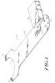
- An implementation of such an inventionis illustrated in Fig. 1 .
- the paddle arm-finger assembly 10is composed of a paddle arm 12 upon which are mounted a plurality of fixed fingers 16 and the mechanism 20 for moving a movable finger 18.
- the paddle 12has a throw sufficient to place the fingers on opposite sides of a wafer.
- the paddle arm/finger assembly 10 heightis compact enough to allow the paddle to be placed between wafers or beneath a wafer and engage the wafer from below.
- the implementation illustrated in figure 1utilizes two fixed fingers 16 at the distal end 150 of the paddle 12 in a spaced relationship so that the two fixed fingers 16 and the moving finger 18 form a triangle of contacts around the edge of any wafer.
- the moving finger 18is attached to a mechanism covered by a housing 20, the mechanism is permanently fixed to the proximate end 17. The moving finger 18 is moved such that the distance between the moving finger 18 and the fixed fingers 16 is decreased when the mechanism is actuated.
- the edge of the wafer 14is engaged by the fixed fingers 16 and the finger tip 40 mounted on the moving finger 18. Once the fingers 16 and 18 have gripped the wafer, the entire paddle arm/finger assembly 10 can move to transport the wafer as needed and as programmed into a robot which moves the paddle arm.
- the detail of the fixed finger 30 that is fixed at the distal end 150 of the paddle arm 12is shown in figure 3 .
- the fixed finger 30is composed of a body 35 and a flexible portion 37.
- the body 35is positioned on the paddle such that a first face 33 faces the wafer.
- the face 33is composed of two parts; a notch 35 in the top portion and inclined plane 32 in the lower portion.
- the body 35is secured to the paddle 12 by its bottom surface 31.
- the mounting means illustratedis a set of holes 36 for bolts to pass through securing the body 35 to the paddle 12.
- the flexible portion 37 of the fixed fingeris parallel to the back radial face 29 of the body 35.
- the flexible portion 37has a fixed end 28, fixed to the body 35 on the back radial face 29 and spacing the remainder of the flexible portion 37 from the body 35 by a distance.
- the flexible portion 37runs parallel to the back radial face 29 of the body 35 and a flexible finger 39 extends perpendicular to the flexible portion 37 and runs parallel to the side of the body 27.
- the flexible finger 39extends at least to the outer edge of notch 34 and is terminated in a flexure tip 37.
- the entire fixed fingeris made of a resilient material so that a force pushing against flexure tip 37 will displace the flexible portion.
- the fixed fingeris a molded piece of polymer, preferably Poly Ether Ether Ketone (PEEK). Alternately the fixed finger can be machined from PEEK. Using PEEK to manufacture the fixed finger is preferred because it does not deteriorate, which could create particulate matter to contaminate wafers, and because it exhibits a suitable springiness to implement the flexure tip.
- the body 35 of the fixed fingeris secured to the paddle using bolts passing through holes 36 to fasten the body 35 to the paddle 12.
- the inclined plane 32serves as a lead-in to guide the edge 14 of the wafer 15 toward the notch 34.
- the notch 34has a span greater than the thickness of the wafer 15 and a depth sufficient to grip the wafer 15 at two points on the notch 34.
- the flexible portion 37 of the fixed finger 30is fixed to the body 35 and spaced apart from it by a small bridge portion 28.
- the center of the bridge portion 28serves as a pivot point for the flexible portion 37.
- the flexible portion 37extends the width of the body 35 and when it has cleared the body, a flexible finger 39 extends perpendicular to the flexible portion 37. While a 90° angle may be used to join the flexible finger 39 to the flexible portion 37, more complex curves serving the same function may be used such as the one illustrated in Fig. 3 .
- Such complex curvesare designed to allow the springiness of the flexure tip 37 to be calibrated to respond to the force that will be applied by the opposing moving finger 19.
- the length of the flexible finger 37is selected to be approximately flush with the edges of the notch 34.
- the moving-finger tip 40is illustrated in figure 4 . It has a body 48, mounting holes 46, inclined plane 42 and an upper portion of its radial face 44.
- the moving-finger tipis a molded piece of polymer, preferably Poly Ether Ether Ketone (PEEK). Using PEEK to manufacture the moving-finger tip is preferred because it does not deteriorate, which could create particulate matter to contaminate wafers.
- the mounting holes 46secure the moving-finger tip 40 to the moving finger 18 that is connected to the mechanism that will move the finger tip 40.
- the inclined plane 42serves as a lead in, like the lead in on the fixed finger, and leads the wafer to the upper portion 48 of the body 44.
- the upper portion 48 of the body 44can be shaped as a notch identical to the notch of the fixed finger 30 or can be an alternate shape. In a preferred embodiment, the upper portion is shaped as a V-shaped notch.
- the moving-finger tip 40is mounted to an effector mechanism 50 as shown in figure 5 .
- the effector mechanism 50is composed of a flexure hinge 55 and bellows 52.
- the flexure hinge 55is composed of a set of stable ends 56 and 60 connected by a pair of flexible arms 58 forming a rectangle when no force is applied.
- Flexible arms 58are composed of a straight length 57 terminated at each end by a flexure notch 53.
- a bellows 52is mounted on one flexible arm 58 near the junction with a stable end.
- First stable end 56mounts the flexure hinge 55 and second stable end 60 has mounted to it the moving finger 18.
- the moving finger 18may incorporate a right angle 19 that causes the moving finger tip 40 to travel in the same direction as the second stable end 60.
- the flexure notches 53 in the flexible arms 58permit the flexible arms 58 to be deflected.
- Bellows 52has a sealed end 51 and has a compressible fluid input port 54 at the second end. Sealed end 51 is mounted to one flexure arm 58 at the junction with first stable end 56. If the bellows input port 54 is held fixed when a compressible fluid enters bellows 52 sealed end 51 exerts a force on flexible arm 58 deflecting it from perpendicular to first stable end 56.
- the deflection near the first stable end 56translates to a larger horizontal deflection at the second stable end 60.
- This deflectionis mirrored in the movement of the movable-finger tip 40.
- the only parts of the effector mechanism 50 that moveare the bellows 52 which expand slightly to exert force on the flexible arm 58 and the second stable end 60 which moves because the flexible arms 58 deflect. Therefore, this movement is free of any friction that could create particulate matter that could contaminate the wafer.
- the flexure arms and stable ends 56 and 60form a parallelogram that is a rectangle at rest. Because of the flexible notch 53, the flexure arm/fixed end junction can be flexed when the compressible fluid in the belows 52 applies pressure.
- Figure 6illustrates how the bellows 52 moves the flexure arm 58.
- the flexed end 56has corners 72 and 74. At rest the flexure arms are in position 82 and 84 attached to the movable stable end 60 having corners 76 and 78.
- points 72 and 74remain stationary while points 76 and 78 are moved to new position 76' and 78' displaced and slightly lower than the position 76, and 78.
- Finger 18is shown in its relaxed position 80 and its displaced position 80'. It can be seen that a small initial displacement of flexure arms 82 and 84 near the fixed end 72/74 causes a larger displacement 76 to 76' at the far end of the arm.
- FIG. 8An alternate embodiment of the effector mechanism is illustrated in Fig. 8 .
- the flexure hinge 50is no longer machined from a single piece of material, and the flexible arms 92 are made of thin flexible metallic material.
- the stable ends 56 and 60can be implemented essentially as implemented in the previous embodiment, while the flexible arms 92 are now attached to the stable ends 56 and 60 such as by brazing, or being bolted on.
- the bellowsare mounted to the movable stable end 60.
- the operation of this flexure hingeis similar to other implementations.
- the bellows 52expands, it places force on the movable stable end 60.
- the flexible arms 92are made of leaf spring material, the force of the bellows displaces the movable stable end.
- the flexible armsassure that the displacement is along the correct axis and that the movable end returns to the rest position when the force is removed.
- a mounting mechanism 20is provided for the effector mechanism 50 as illustrated in Fig. 7 .
- the fixed stable end 56is mounted to one wall 84 of the mounting mechanism 20.
- a slot 82 in the opposite wall 86 of the mounting mechanism 20allows the moving finger 18 to pass through the enclosure.
- the bellows 52is mounted between a flexure arm 58 and a sidewall 54 with the intake 54 passing through the sidewall 54. When compressible fluid is forced into bellows 52, the flexure arm 58 is deflected and the moving finger 18 holding the moving-finger tip 40 is deflected a larger amount engaging the wafer edge 14 and pushing the wafer 15 into the notches 34 in the fixed fingers 16.
- the force exerted by the moving-finger tip 40is sufficient to displace the flexure tip 39 holding it in tension until the movingfinger tip 40 releases the wafer edge 14.
- the paddle arm assemblyprovides a suitable platform for the mounting of sensors such as ones to detect a wafer, detect closed fingers or detect open fingers, as may be needed to assure correct operation of the apparatus.
Landscapes
- Engineering & Computer Science (AREA)
- Robotics (AREA)
- Physics & Mathematics (AREA)
- Condensed Matter Physics & Semiconductors (AREA)
- General Physics & Mathematics (AREA)
- Manufacturing & Machinery (AREA)
- Computer Hardware Design (AREA)
- Microelectronics & Electronic Packaging (AREA)
- Power Engineering (AREA)
- Container, Conveyance, Adherence, Positioning, Of Wafer (AREA)
- Manipulator (AREA)
Description
- Silicon wafers for semiconductor production pass through many steps in transitioning from a slice of silicon to a collection of functional integrated circuits on a silicon wafer. Between many of these steps the wafers must be removed from a cassette, have their orientation changed, be placed in fixtures and be transported to the next step. All of these operations are performed in a clean room. One of the present technologies in wafer handling uses backside contact by vacuum grippers. This technology requires that there be a front side of the wafer and a backside with the backside subject to being handled by the vacuum grippers. A second technology in wafer handling grips the wafers by the edges but is subject to sudden exertions of force and mechanism wear that causes contamination. Both of these technologies have suffered from wafer jams when inserting and removing the wafers from the cassette, the wafer protrusion problem-misalignment of the wafers in the cassette, and contaminants getting on the wafer from breakdown of the transport mechanism.
US-A-4944650 discloses an edge gripping wafer handling apparatus for selectively securing and transporting wafers comprising:- a paddle arm configured to be supported and moved by a wafer handling apparatus ;
- a plurality of fixed fingers attached to said paddle arm operative to engage an edge of a wafer;
- a moving finger operable to engage said edge of said wafer through movement towards said plurality of fixed fingers ;
- wherein only said edge extending around a circumference of said wafer is gripped by said moving finger and said plurality of fixed fingers and said engaging results from said movement of said moving finger towards said fixed fingers.
- The present invention relates to handling of silicon wafers and in particular to edge grip handling of silicon wafers.
- The invention is defined in claims 1 and 22. Various embodiments are defined in the dependent claims.
- A stable edge grip on a wafer can be maintained if there are at least three points of contact between the gripper and the wafer. The force imparted by the three points of contact must be sufficient to counterbalance the weight of the wafer, but must not be so large as to bend the wafer significantly. At least three edge gripping fingers are mounted on a paddle such that the entire paddle/finger assembly can fit between wafers in a cassette. At least two of the edge gripping fingers are fixed at one end of the paddle in a separated relationship and passively respond to pressure brought to bear on them by the wafer. A single finger acting is mounted on the other end of the paddle and exhibits linear motion. The arrangement of the fingers on opposite sides of the wafer leaves the edges along the axis of the paddle arm free. The movable finger is brought into contact with the wafer by a flexure hinge driven by compressible fluid. Because there is no rubbing motion in the mechanism of the flexure hinge, the mechanism does not wear, does not have backlash or creep-like error motions, and no particulate contaminants are generated. In addition, the use of a compressible fluid mechanism assures that a smooth steady motion is imparted to the moving finger.
- In picking up a wafer, the paddle/finger assembly is slid beneath the target wafer until the two fixed fingers are just past the edge of the wafer. The assembly is then raised so that the wafer and gripping surface of all the fingers are approximately aligned. The moving finger then moves toward the wafer until it exerts sufficient force on the wafer to bring the far side of the wafer in contact with the fixed fingers. The moving finger is maintained in the contact position throughout the withdrawal from the cassette and during any transport.
- The release of the wafer is accomplished by reversing the steps of pickup. The moving finger breaks contact with the wafer releasing the force on the wafer. A flexure tip on the fixed fingers nudges the wafer away from edge gripping surface of the fixed fingers. Then the paddle/finger assembly is lowered and withdrawn from the proximity of the wafer.
- An edge gripping wafer handling apparatus according to the invention and a method for gripping a wafer according to the invention are defined in the appended claims.
- The invention as disclosed herein will be more fully understood by reference to the following detailed description and drawings, of which:
Fig. 1 shows the paddle, fixed fingers and moving finger;Fig. 2 shows the paddle, fixed fingers and moving finger securing a wafer;Fig. 3 shows a fixed finger flexure fixture;Fig. 4 shows the moving finger tip;Fig. 5 shows a flexure hinge supporting the moving finger with a bellows attached;Fig. 6 illustrates the flexing of the flexure hinge when the bellows applies force;Fig. 7 shows the effector mechanism mounted in a housing with the moving finger led outside the housing; andFig. 8 shows an alternate embodiment of a flexure hinge.- The advantages of edge gripping silicon wafers come about because gripping by the edge frees both surfaces for processing. The surfaces are not contaminated nor are they obscured by the gripping fingers. In addition, by gripping the edges of a wafer the wafer itself can be precisely placed in a fixture without the probability that it will shift.
- The general concept of the invention is that fingers will be used to grip the edge of the wafers. Such fingers are to be spread around the periphery of the wafer. Only one finger will be actively driven by any mechanism. The mechanism is based on the bending of a structure that causes no rubbing or other friction. The fixed fingers utilized to grip the wafer will have a passive response rather than being inert. An implementation of such an invention is illustrated in
Fig. 1 . The paddle arm-finger assembly 10 is composed of apaddle arm 12 upon which are mounted a plurality offixed fingers 16 and themechanism 20 for moving amovable finger 18. Thepaddle 12 has a throw sufficient to place the fingers on opposite sides of a wafer. The paddle arm/finger assembly 10 height is compact enough to allow the paddle to be placed between wafers or beneath a wafer and engage the wafer from below. - The implementation illustrated in
figure 1 utilizes twofixed fingers 16 at thedistal end 150 of thepaddle 12 in a spaced relationship so that the twofixed fingers 16 and the movingfinger 18 form a triangle of contacts around the edge of any wafer. At the proximate end 17 of the paddle arm, the movingfinger 18 is attached to a mechanism covered by ahousing 20, the mechanism is permanently fixed to the proximate end 17. The movingfinger 18 is moved such that the distance between the movingfinger 18 and thefixed fingers 16 is decreased when the mechanism is actuated. - When a
wafer 15 is engaged by the paddle arm/finger assembly 10 as illustrated infigure 2 , the edge of thewafer 14 is engaged by thefixed fingers 16 and thefinger tip 40 mounted on the movingfinger 18. Once thefingers finger assembly 10 can move to transport the wafer as needed and as programmed into a robot which moves the paddle arm. - The detail of the fixed
finger 30 that is fixed at thedistal end 150 of thepaddle arm 12 is shown infigure 3 . The fixedfinger 30 is composed of abody 35 and aflexible portion 37. Thebody 35 is positioned on the paddle such that afirst face 33 faces the wafer. Theface 33 is composed of two parts; anotch 35 in the top portion andinclined plane 32 in the lower portion. Thebody 35 is secured to thepaddle 12 by itsbottom surface 31. Infigure 3 , the mounting means illustrated is a set ofholes 36 for bolts to pass through securing thebody 35 to thepaddle 12. Theflexible portion 37 of the fixed finger is parallel to the backradial face 29 of thebody 35. Theflexible portion 37 has a fixedend 28, fixed to thebody 35 on the backradial face 29 and spacing the remainder of theflexible portion 37 from thebody 35 by a distance. Theflexible portion 37 runs parallel to the backradial face 29 of thebody 35 and aflexible finger 39 extends perpendicular to theflexible portion 37 and runs parallel to the side of thebody 27. Theflexible finger 39 extends at least to the outer edge ofnotch 34 and is terminated in aflexure tip 37. - The entire fixed finger is made of a resilient material so that a force pushing against
flexure tip 37 will displace the flexible portion. In a preferred embodiment, the fixed finger is a molded piece of polymer, preferably Poly Ether Ether Ketone (PEEK). Alternately the fixed finger can be machined from PEEK. Using PEEK to manufacture the fixed finger is preferred because it does not deteriorate, which could create particulate matter to contaminate wafers, and because it exhibits a suitable springiness to implement the flexure tip. - The
body 35 of the fixed finger is secured to the paddle using bolts passing throughholes 36 to fasten thebody 35 to thepaddle 12. Theinclined plane 32 serves as a lead-in to guide theedge 14 of thewafer 15 toward thenotch 34. Thenotch 34 has a span greater than the thickness of thewafer 15 and a depth sufficient to grip thewafer 15 at two points on thenotch 34. - The
flexible portion 37 of the fixedfinger 30 is fixed to thebody 35 and spaced apart from it by asmall bridge portion 28. The center of thebridge portion 28 serves as a pivot point for theflexible portion 37. Theflexible portion 37 extends the width of thebody 35 and when it has cleared the body, aflexible finger 39 extends perpendicular to theflexible portion 37. While a 90° angle may be used to join theflexible finger 39 to theflexible portion 37, more complex curves serving the same function may be used such as the one illustrated inFig. 3 . Such complex curves are designed to allow the springiness of theflexure tip 37 to be calibrated to respond to the force that will be applied by the opposing movingfinger 19. The length of theflexible finger 37 is selected to be approximately flush with the edges of thenotch 34. When thepaddle 12 is brought in contact with awafer 15, theflexible tip 37 is in contact with theedge 14 of thewafer 15. - The moving-
finger tip 40 is illustrated infigure 4 . It has abody 48, mountingholes 46,inclined plane 42 and an upper portion of itsradial face 44. In a preferred embodiment, the moving-finger tip is a molded piece of polymer, preferably Poly Ether Ether Ketone (PEEK). Using PEEK to manufacture the moving-finger tip is preferred because it does not deteriorate, which could create particulate matter to contaminate wafers. The mounting holes 46 secure the moving-finger tip 40 to the movingfinger 18 that is connected to the mechanism that will move thefinger tip 40. Theinclined plane 42 serves as a lead in, like the lead in on the fixed finger, and leads the wafer to theupper portion 48 of thebody 44. Theupper portion 48 of thebody 44 can be shaped as a notch identical to the notch of the fixedfinger 30 or can be an alternate shape. In a preferred embodiment, the upper portion is shaped as a V-shaped notch. - The moving-
finger tip 40 is mounted to aneffector mechanism 50 as shown infigure 5 . Theeffector mechanism 50 is composed of aflexure hinge 55 and bellows 52. Theflexure hinge 55 is composed of a set of stable ends 56 and 60 connected by a pair offlexible arms 58 forming a rectangle when no force is applied.Flexible arms 58 are composed of astraight length 57 terminated at each end by aflexure notch 53. A bellows 52 is mounted on oneflexible arm 58 near the junction with a stable end. Firststable end 56 mounts theflexure hinge 55 and secondstable end 60 has mounted to it the movingfinger 18. Depending on the orientation of the mechanism to the moving finger, the movingfinger 18 may incorporate aright angle 19 that causes the movingfinger tip 40 to travel in the same direction as the secondstable end 60. Theflexure notches 53 in theflexible arms 58 permit theflexible arms 58 to be deflected.Bellows 52 has a sealedend 51 and has a compressiblefluid input port 54 at the second end.Sealed end 51 is mounted to oneflexure arm 58 at the junction with firststable end 56. If thebellows input port 54 is held fixed when a compressible fluid entersbellows 52 sealedend 51 exerts a force onflexible arm 58 deflecting it from perpendicular to firststable end 56. The deflection near the firststable end 56 translates to a larger horizontal deflection at the secondstable end 60. This deflection is mirrored in the movement of the movable-finger tip 40. The only parts of theeffector mechanism 50 that move are thebellows 52 which expand slightly to exert force on theflexible arm 58 and the secondstable end 60 which moves because theflexible arms 58 deflect. Therefore, this movement is free of any friction that could create particulate matter that could contaminate the wafer. The flexure arms and stable ends 56 and 60 form a parallelogram that is a rectangle at rest. Because of theflexible notch 53, the flexure arm/fixed end junction can be flexed when the compressible fluid in thebelows 52 applies pressure.Figure 6 illustrates how thebellows 52 moves theflexure arm 58. Theflexed end 56 hascorners position stable end 60 havingcorners points new position 76' and 78' displaced and slightly lower than theposition Finger 18 is shown in itsrelaxed position 80 and its displaced position 80'. It can be seen that a small initial displacement offlexure arms fixed end 72/74 causes alarger displacement 76 to 76' at the far end of the arm. Displacement of tip is given by :
where theta is the displacement angle at the fixed end, theta is defined by the material from which the effector mechanism is fabricated,
- E is the Young's modulus of the material and M is the bending moment of each of the notches expressed as

- The remaining variables are illustrated on
Fig 5 .
In one embodiment, using 70-79 T6 Aluminium and variables of
L=6.35 cm (L=2.5 in.), R=0.9525 cm (R=0.375in.), t=0.03175 cm (t=0.0125 in.), b=0.635 cm (b=0.25 in.),
L1=1.529 cm (L1=0.602 in) and F=2.27 kg (F=5 Ib.), the tip will move 1.7958 cm (0.707 in.).
the above equations apply when bellows 52 are mounted further away from the fixedend 56 than shown inFig. 5 . This may be desirable for a modified mounting arrangement and alternate compressible fluids. - An alternate embodiment of the effector mechanism is illustrated in
Fig. 8 . Here theflexure hinge 50 is no longer machined from a single piece of material, and theflexible arms 92 are made of thin flexible metallic material. The stable ends 56 and 60 can be implemented essentially as implemented in the previous embodiment, while theflexible arms 92 are now attached to the stable ends 56 and 60 such as by brazing, or being bolted on. In this embodiment, the bellows are mounted to the movablestable end 60. The operation of this flexure hinge is similar to other implementations. When the bellows 52 expands, it places force on the movablestable end 60.
When theflexible arms 92 are made of leaf spring material, the force of the bellows displaces the movable stable end. The flexible arms assure that the displacement is along the correct axis and that the movable end returns to the rest position when the force is removed. - A mounting
mechanism 20 is provided for theeffector mechanism 50 as illustrated inFig. 7 . The fixedstable end 56 is mounted to onewall 84 of the mountingmechanism 20. Aslot 82 in the opposite wall 86 of the mountingmechanism 20 allows the movingfinger 18 to pass through the enclosure. The bellows 52 is mounted between aflexure arm 58 and asidewall 54 with theintake 54 passing through thesidewall 54. When compressible fluid is forced intobellows 52, theflexure arm 58 is deflected and the movingfinger 18 holding the moving-finger tip 40 is deflected a larger amount engaging thewafer edge 14 and pushing thewafer 15 into thenotches 34 in the fixedfingers 16. The force exerted by the moving-finger tip 40 is sufficient to displace theflexure tip 39 holding it in tension until themovingfinger tip 40 releases thewafer edge 14. The paddle arm assembly provides a suitable platform for the mounting of sensors such as ones to detect a wafer, detect closed fingers or detect open fingers, as may be needed to assure correct operation of the apparatus. - It will now become apparent to those of ordinary skill in the art that other embodiments incorporating these concepts may be used. Accordingly, it is submitted that the invention should not be limited by the described embodiments but rather should only be limited by the scope of the appended claims.


Claims (22)
- An edge gripping wafer handling apparatus (10) for selectively securing and transporting wafers comprising:a paddle arm (12) configured to be supported and moved by a wafer handling apparatus (10);a plurality of fixed fingers (16) attached to said paddle arm (12) operative to engage an edge (14) of a wafer (15), wherein each fixed finger of said plurality of fixed fingers (16) has a face (33) comprising a finger wafer notch (34) in its top portion, operative to secure said wafer (15), a beveled finger edge (32) in its lower portion, to guide the edge of said wafer toward said finger wafer notch (34) and a flexible portion (37) extending toward said face and terminating beyond said finger wafer notch (34) and before said beveled finger edge (32), said flexible portion being adapted to be displaced by said wafer edge (14) when said wafer edge (14) is secured in said notch (34);a moving finger (18) operable to engage said edge (14) of said wafer (15) through movement towards said plurality of fixed fingers (16);wherein only said edge extending around the circumference of said wafer (15) is gripped by said moving finger (18) and said plurality of fixed fingers (16) and said engaging results from said movement of said moving finger (18) towards said fixed fingers (16).
- The apparatus of claim 1 wherein said paddle arm (12) has a length greater than the diameter of said wafer.
- The apparatus of claim 1 wherein a distal end portion of said paddle arm (12) is forked forming tines and said plurality of fixed fingers (16) are disposed with one of said plurality of fixed fingers (16) per tine of said forked distal end portion.
- The apparatus of claim 1 wherein said paddle arm (12) comprises a material of sufficient strength to remain rigid under operational conditions.
- The apparatus of claim 1 wherein said plurality of fixed fingers (16) and said moving finger (18) are disposed on said paddle arm (12) to be positioned on substantially opposed edges of said wafer (15).
- The apparatus of claim 1 wherein said plurality of fixed fingers (16) is two fixed fingers.
- The apparatus of claim 1 wherein said plurality of fixed fingers (16) are made non-conductive, non-static, non-particulate generating polymer.
- The apparatus of claim 1 wherein said plurality of fixed fingers (16) are made of Poly Ether Ether Ketone PEEK.
- The apparatus of claim 1 wherein said finger wafer notch (34) is V-shaped and the opening of said finger wafer notch is greater than the thickness of said wafer (15).
- The apparatus of claim 1 wherein said flexible portion (37) is configured to be displaced to said wafer edge (14) when said wafer edge (14) is secured in said finger wafer notch (34).
- The apparatus of claim 1 wherein said moving finger (18) is terminated by a moving finger tip (40) having a face comprising a finger wafer notch (48) in its top portion, adapted to secure said wafer and a beveled finger edge (42) in its lower portion, to guide the edge of said wafer toward said finger wafer notch (48).
- The apparatus of claim 11 wherein said moving finger tip (40) is made of PEEK.
- The apparatus of claim 11 wherein said beveled finger edge (42) is angled towards said finger wafer notch (48) and said finger wafer notch (48) extends across said face of said moving finger tip (40) such that said beveled finger edge (42) disposes said wafer (15) into contact with said finger wafer notch (48) as said beveled finger edge (42) is slideable engaged with said wafer.
- The apparatus of claim 1 wherein said moving finger (18) is disposed on an effector mechanism (50) attached at a proximate end portion of said paddle arm (12), said effector mechanism (50) comprising a flexure hinge (55) structured for resilient movement and a bellows (52) configured for expansionary displacement, said bellows (52) operable to move said flexure hinge (55) by said expansionary displacement and said flexure hinge (55) comprising a fixed end portion (56) and a movable end portion (60).
- The apparatus of claim 14 wherein said expansionary displacement is provided by a compressible fluid forced into said bellows (52).
- The apparatus of claim 15 wherein said compressible fluid is compressed air and said bellows (52) has a compressed air entry aperture (54) at an end distal from said flexure hinge (55).
- The apparatus of claim 14 wherein said flexure hinge (55) further comprises at least one flexure arm (58) of a leaf spring material disposed between said fixed end portion (56) and said movable end portion (60), said leaf spring material produced for temporary deflection.
- The apparatus of claim 17 wherein said temporary deflection provides said resilient movement of a flexure hinge (55).
- The apparatus of claim 18 wherein said resilient movement is smooth and creates no particulate matter.
- The apparatus of claim 14 wherein said effector mechanism (50) is cased in an enclosure (20), said enclosure mounted to said proximate end portion of said paddle arm (12), and said hinge fixed end portion (56) attached to said enclosure (20) and said movable end portion (60) attached to said moving finger (18), said moving finger (18) passing through a slot (82) in said enclosure (20).
- The apparatus of claim 1 wherein said flexible portion (37) has a flexible tip constructed to retract when a force is applied radially and return to a rest position when said force is removed.
- A method for gripping a wafer (15) having an edge (14) extending around its circumference, comprising:disposing a paddle arm/finger assembly (10) below said wafer (15) and aligned such that a face of each finger of a set of fingers (16, 18), comprising one moving finger (18) and a plurality of fixed fingers (16), of said finger assembly are proximate but external to said edge (14) of said wafer (15);wherein said face of each fixed finger of said plurality of fixed fingers (16) has a finger wafer notch (34) in the top portion of said face, operative to secure said wafer (15), a beveled finger edge (32) in the lower portion of said face, to guide the edge of said wafer toward said finger wafer notch (34) and a flexible portion (37) extending toward said face and terminating beyond said finger wafer notch (34) and before said beveled finger edge (32); said flexible portion (37) being adapted to be displaced by said wafer edge (14) when said wafer edge (14) is secured in said notch (34);raising said paddle arm/finger assembly until said beveled finger edge (32, 42) disposed in the lower portion of said face on each finger of said set of fingers is abutting a lower surface of said wafer (15);moving said moving finger (18) toward the center of said wafer (15) to engage said edge of said wafer (15) in a notch in said face of said moving finger (18) until said edge of said wafer (15) engages all faces of said plurality of fixed fingers (16), and continuing said movement of said moving finger (18) until said edge extending around said circumference of said wafer (15) is secured in said finger wafer notches and said flexible portion is displaced by said wafer edge (14).
Applications Claiming Priority (3)
| Application Number | Priority Date | Filing Date | Title |
|---|---|---|---|
| US13245599P | 1999-05-04 | 1999-05-04 | |
| US132455P | 1999-05-04 | ||
| PCT/US2000/012018WO2000066480A2 (en) | 1999-05-04 | 2000-05-03 | Edge gripping end effector wafer handling apparatus |
Publications (3)
| Publication Number | Publication Date |
|---|---|
| EP1313662A2 EP1313662A2 (en) | 2003-05-28 |
| EP1313662A4 EP1313662A4 (en) | 2009-05-06 |
| EP1313662B1true EP1313662B1 (en) | 2014-03-26 |
Family
ID=22454133
Family Applications (1)
| Application Number | Title | Priority Date | Filing Date |
|---|---|---|---|
| EP00926507.5AExpired - LifetimeEP1313662B1 (en) | 1999-05-04 | 2000-05-03 | Edge gripping end effector wafer handling apparatus |
Country Status (4)
| Country | Link |
|---|---|
| US (1) | US6491330B1 (en) |
| EP (1) | EP1313662B1 (en) |
| JP (1) | JP4097404B2 (en) |
| WO (1) | WO2000066480A2 (en) |
Families Citing this family (26)
| Publication number | Priority date | Publication date | Assignee | Title |
|---|---|---|---|---|
| US7175214B2 (en)* | 2000-03-16 | 2007-02-13 | Ade Corporation | Wafer gripping fingers to minimize distortion |
| US7334826B2 (en)* | 2001-07-13 | 2008-02-26 | Semitool, Inc. | End-effectors for handling microelectronic wafers |
| US7281741B2 (en)* | 2001-07-13 | 2007-10-16 | Semitool, Inc. | End-effectors for handling microelectronic workpieces |
| US20060043750A1 (en)* | 2004-07-09 | 2006-03-02 | Paul Wirth | End-effectors for handling microfeature workpieces |
| US20070014656A1 (en)* | 2002-07-11 | 2007-01-18 | Harris Randy A | End-effectors and associated control and guidance systems and methods |
| USD491427S1 (en) | 2002-08-30 | 2004-06-15 | David Weimer | Universal camshaft retainer |
| US7300082B2 (en)* | 2003-07-21 | 2007-11-27 | Asyst Technologies, Inc. | Active edge gripping and effector |
| US20050110287A1 (en)* | 2003-10-24 | 2005-05-26 | Ade Corporation | 200 MM notched/flatted wafer edge gripping end effector |
| US20070020080A1 (en)* | 2004-07-09 | 2007-01-25 | Paul Wirth | Transfer devices and methods for handling microfeature workpieces within an environment of a processing machine |
| US7344352B2 (en)* | 2005-09-02 | 2008-03-18 | Axcelis Technologies, Inc. | Workpiece transfer device |
| DE102006038243A1 (en)* | 2006-08-14 | 2008-02-28 | Qimonda Ag | Method and device for handling an article in the context of a semiconductor production |
| US7789443B2 (en)* | 2007-03-16 | 2010-09-07 | Axcelis Technologies, Inc. | Workpiece gripping device |
| US9437469B2 (en)* | 2007-04-27 | 2016-09-06 | Brooks Automation, Inc. | Inertial wafer centering end effector and transport apparatus |
| JP4871910B2 (en)* | 2007-05-16 | 2012-02-08 | 株式会社日立ハイテクノロジーズ | Disc chuck mechanism and disc handling robot |
| USD674366S1 (en)* | 2011-01-20 | 2013-01-15 | Tokyo Electron Limited | Wafer holding member |
| USD674761S1 (en)* | 2011-10-20 | 2013-01-22 | Tokyo Electron Limited | Wafer holding member |
| CN103192401B (en)* | 2012-01-05 | 2015-03-18 | 沈阳新松机器人自动化股份有限公司 | Manipulator end effector |
| US9536764B2 (en) | 2015-01-27 | 2017-01-03 | Lam Research Corporation | End effector for wafer transfer system and method of transferring wafers |
| EP3389954A1 (en) | 2015-12-16 | 2018-10-24 | Comau LLC | Adaptable end effector and method |
| US10133186B2 (en) | 2016-10-20 | 2018-11-20 | Mapper Lithography Ip B.V. | Method and apparatus for aligning substrates on a substrate support unit |
| JP6580544B2 (en)* | 2016-10-20 | 2019-09-25 | エーエスエムエル ネザーランズ ビー.ブイ. | Method and apparatus for aligning a substrate on a substrate support unit |
| US9919430B1 (en)* | 2016-12-06 | 2018-03-20 | Jabil Inc. | Apparatus, system and method for providing an end effector |
| US11020852B2 (en) | 2017-10-05 | 2021-06-01 | Brooks Automation, Inc. | Substrate transport apparatus with independent accessory feedthrough |
| US11565406B2 (en)* | 2020-11-23 | 2023-01-31 | Mitsubishi Electric Research Laboratories, Inc. | Multi-tentacular soft robotic grippers |
| US20230373100A1 (en)* | 2022-05-19 | 2023-11-23 | Taiwan Semiconductor Manufacturing Co., Ltd. | Transfer blade for robot |
| USD1077046S1 (en)* | 2022-12-01 | 2025-05-27 | Koninklijke Philips N.V. | Handle for nanoimprinting machine |
Family Cites Families (22)
| Publication number | Priority date | Publication date | Assignee | Title |
|---|---|---|---|---|
| US3967946A (en)* | 1972-12-15 | 1976-07-06 | Emhart Corporation | Mold holder arms for glassware forming machine and method of operating the same |
| US4030622A (en) | 1975-05-23 | 1977-06-21 | Pass-Port Systems, Inc. | Wafer transport system |
| US4410209A (en)* | 1982-03-11 | 1983-10-18 | Trapani Silvio P | Wafer-handling tool |
| CA1276710C (en)* | 1983-11-30 | 1990-11-20 | Kazuo Asakawa | Robot force controlling system |
| US4813732A (en)* | 1985-03-07 | 1989-03-21 | Epsilon Technology, Inc. | Apparatus and method for automated wafer handling |
| US4762353A (en) | 1987-03-09 | 1988-08-09 | Dexon, Inc. | Flexible carrier for semiconductor wafer cassettes |
| US4745812A (en) | 1987-03-25 | 1988-05-24 | The United States Of America As Represented By The Secretary Of The Army | Triaxial tactile sensor |
| JP2508540B2 (en)* | 1987-11-02 | 1996-06-19 | 三菱マテリアル株式会社 | Wafer position detector |
| KR900006017B1 (en)* | 1987-12-18 | 1990-08-20 | 한국전기통신공사 | Variable Diameter Wafer Transporter |
| US4854623A (en) | 1988-01-29 | 1989-08-08 | Dexton, Inc. | End effector |
| US4900214A (en)* | 1988-05-25 | 1990-02-13 | American Telephone And Telegraph Company | Method and apparatus for transporting semiconductor wafers |
| US5061144A (en)* | 1988-11-30 | 1991-10-29 | Tokyo Electron Limited | Resist process apparatus |
| US5046773A (en)* | 1990-01-02 | 1991-09-10 | Hewlett-Packard Company | Micro-gripper assembly |
| US5429251A (en) | 1993-09-22 | 1995-07-04 | Legacy Systems, Inc. | Semiconductor wafer end effector |
| JP3143770B2 (en)* | 1994-10-07 | 2001-03-07 | 東京エレクトロン株式会社 | Substrate transfer device |
| US5613821A (en) | 1995-07-06 | 1997-03-25 | Brooks Automation, Inc. | Cluster tool batchloader of substrate carrier |
| FR2746115B1 (en)* | 1996-03-15 | 1998-05-22 | SUBSTRATE SUPPORT FOR EVAPORATION INSTALLATION | |
| US5810549A (en) | 1996-04-17 | 1998-09-22 | Applied Materials, Inc. | Independent linear dual-blade robot and method for transferring wafers |
| US5765983A (en) | 1996-05-30 | 1998-06-16 | Brooks Automation, Inc. | Robot handling apparatus |
| US5778554A (en) | 1996-07-15 | 1998-07-14 | Oliver Design, Inc. | Wafer spin dryer and method of drying a wafer |
| US6155773A (en)* | 1997-09-22 | 2000-12-05 | Applied Materials, Inc. | Substrate clamping apparatus |
| US6322312B1 (en)* | 1999-03-18 | 2001-11-27 | Applied Materials, Inc. | Mechanical gripper for wafer handling robots |
- 2000
- 2000-05-03EPEP00926507.5Apatent/EP1313662B1/ennot_activeExpired - Lifetime
- 2000-05-03JPJP2000615323Apatent/JP4097404B2/ennot_activeExpired - Fee Related
- 2000-05-03WOPCT/US2000/012018patent/WO2000066480A2/enactiveApplication Filing
- 2000-05-03USUS09/565,035patent/US6491330B1/ennot_activeExpired - Lifetime
Also Published As
| Publication number | Publication date |
|---|---|
| EP1313662A4 (en) | 2009-05-06 |
| US6491330B1 (en) | 2002-12-10 |
| JP4097404B2 (en) | 2008-06-11 |
| WO2000066480A2 (en) | 2000-11-09 |
| EP1313662A2 (en) | 2003-05-28 |
| JP2003524881A (en) | 2003-08-19 |
| WO2000066480A3 (en) | 2003-03-13 |
Similar Documents
| Publication | Publication Date | Title |
|---|---|---|
| EP1313662B1 (en) | Edge gripping end effector wafer handling apparatus | |
| US6468022B1 (en) | Edge-gripping pre-aligner | |
| JP4287589B2 (en) | Apparatus, clamp mechanism, arm assembly and method | |
| KR100331157B1 (en) | Wafer holding hand | |
| JP5123851B2 (en) | Work piece container for storing the work piece | |
| KR101475790B1 (en) | Inertial wafer centering end effector and transfer device | |
| TWI226097B (en) | Method and apparatus for transferring a thin plate, and manufacturing method of substrate using the same | |
| EP0778611A2 (en) | End effector for semiconductor wafer transfer device and method of moving a wafer with an end effector | |
| US6623235B2 (en) | Robot arm edge gripping device for handling substrates using two four-bar linkages | |
| WO2007028074A2 (en) | Workpiece transfer device | |
| WO2000033359B1 (en) | Specimen holding robotic arm end effector | |
| US6948898B2 (en) | Alignment of semiconductor wafers and other articles | |
| JP2004535681A (en) | Centered bilateral edge grip end effector with integrated mapping sensor | |
| JPH1064976A (en) | Piezoelectric wafer gripper for robot blade | |
| US20190148210A1 (en) | Substrate transfer hand and robot | |
| CN1824592A (en) | Wafer transfer device | |
| US7712808B2 (en) | End effector with centering grip | |
| US20030133780A1 (en) | Robot arm edge gripping device for handling substrates | |
| KR102822337B1 (en) | Gripper Assembly and Method for operating the Gripper Assembly | |
| KR20050045828A (en) | Apparatus for mounting semiconductor chips | |
| EP3655352A1 (en) | Non-contact handler and method of handling workpieces using the same | |
| EP0585508A1 (en) | A device for gripping sheet-like workpieces | |
| CN117467979A (en) | Wafer position calibration device and chemical vapor deposition equipment using same | |
| JPH02246241A (en) | Manufacture of semiconductor device |
Legal Events
| Date | Code | Title | Description |
|---|---|---|---|
| PUAI | Public reference made under article 153(3) epc to a published international application that has entered the european phase | Free format text:ORIGINAL CODE: 0009012 | |
| 17P | Request for examination filed | Effective date:20010509 | |
| AK | Designated contracting states | Designated state(s):DE GB IT | |
| A4 | Supplementary search report drawn up and despatched | Effective date:20090408 | |
| RIC1 | Information provided on ipc code assigned before grant | Ipc:B66F 1/00 20060101AFI20001110BHEP Ipc:H01L 21/68 20060101ALI20090402BHEP | |
| 17Q | First examination report despatched | Effective date:20100629 | |
| GRAP | Despatch of communication of intention to grant a patent | Free format text:ORIGINAL CODE: EPIDOSNIGR1 | |
| INTG | Intention to grant announced | Effective date:20130823 | |
| INTG | Intention to grant announced | Effective date:20130827 | |
| GRAS | Grant fee paid | Free format text:ORIGINAL CODE: EPIDOSNIGR3 | |
| GRAA | (expected) grant | Free format text:ORIGINAL CODE: 0009210 | |
| AK | Designated contracting states | Kind code of ref document:B1 Designated state(s):DE GB IT | |
| REG | Reference to a national code | Ref country code:GB Ref legal event code:FG4D | |
| REG | Reference to a national code | Ref country code:DE Ref legal event code:R096 Ref document number:60048494 Country of ref document:DE Effective date:20140508 | |
| PGFP | Annual fee paid to national office [announced via postgrant information from national office to epo] | Ref country code:GB Payment date:20140527 Year of fee payment:15 | |
| PGFP | Annual fee paid to national office [announced via postgrant information from national office to epo] | Ref country code:DE Payment date:20140529 Year of fee payment:15 | |
| REG | Reference to a national code | Ref country code:DE Ref legal event code:R097 Ref document number:60048494 Country of ref document:DE | |
| PLBE | No opposition filed within time limit | Free format text:ORIGINAL CODE: 0009261 | |
| STAA | Information on the status of an ep patent application or granted ep patent | Free format text:STATUS: NO OPPOSITION FILED WITHIN TIME LIMIT | |
| 26N | No opposition filed | Effective date:20150106 | |
| PG25 | Lapsed in a contracting state [announced via postgrant information from national office to epo] | Ref country code:IT Free format text:LAPSE BECAUSE OF FAILURE TO SUBMIT A TRANSLATION OF THE DESCRIPTION OR TO PAY THE FEE WITHIN THE PRESCRIBED TIME-LIMIT Effective date:20140326 | |
| REG | Reference to a national code | Ref country code:DE Ref legal event code:R097 Ref document number:60048494 Country of ref document:DE Effective date:20150106 | |
| REG | Reference to a national code | Ref country code:DE Ref legal event code:R119 Ref document number:60048494 Country of ref document:DE | |
| GBPC | Gb: european patent ceased through non-payment of renewal fee | Effective date:20150503 | |
| PG25 | Lapsed in a contracting state [announced via postgrant information from national office to epo] | Ref country code:GB Free format text:LAPSE BECAUSE OF NON-PAYMENT OF DUE FEES Effective date:20150503 Ref country code:DE Free format text:LAPSE BECAUSE OF NON-PAYMENT OF DUE FEES Effective date:20151201 | |
| P01 | Opt-out of the competence of the unified patent court (upc) registered | Effective date:20230525 |