EP1303793B1 - Method and system of automatic fluid dispensing for imprint lithography processes - Google Patents
Method and system of automatic fluid dispensing for imprint lithography processesDownload PDFInfo
- Publication number
- EP1303793B1 EP1303793B1EP01955853.5AEP01955853AEP1303793B1EP 1303793 B1EP1303793 B1EP 1303793B1EP 01955853 AEP01955853 AEP 01955853AEP 1303793 B1EP1303793 B1EP 1303793B1
- Authority
- EP
- European Patent Office
- Prior art keywords
- substrate
- template
- liquid
- patterned template
- gap
- Prior art date
- Legal status (The legal status is an assumption and is not a legal conclusion. Google has not performed a legal analysis and makes no representation as to the accuracy of the status listed.)
- Expired - Lifetime
Links
- 238000000034methodMethods0.000titleclaimsdescription192
- 230000008569processEffects0.000titleclaimsdescription103
- 239000012530fluidSubstances0.000titleclaimsdescription89
- 238000001459lithographyMethods0.000titleclaimsdescription71
- 239000000758substrateSubstances0.000claimsdescription291
- 239000007788liquidSubstances0.000claimsdescription77
- 238000012546transferMethods0.000claimsdescription21
- 230000003213activating effectEffects0.000claimsdescription10
- 230000015572biosynthetic processEffects0.000claimsdescription7
- 238000006073displacement reactionMethods0.000claimsdescription6
- 238000005530etchingMethods0.000claimsdescription6
- 239000010410layerSubstances0.000description78
- 230000033001locomotionEffects0.000description56
- 239000000463materialSubstances0.000description31
- 238000005259measurementMethods0.000description29
- 239000000126substanceSubstances0.000description25
- 230000003287optical effectEffects0.000description23
- 239000010408filmSubstances0.000description22
- 238000004519manufacturing processMethods0.000description21
- 239000003795chemical substances by applicationSubstances0.000description19
- 238000012937correctionMethods0.000description19
- 239000004065semiconductorSubstances0.000description18
- 230000008901benefitEffects0.000description15
- 238000000576coating methodMethods0.000description15
- 238000013461designMethods0.000description14
- 238000012545processingMethods0.000description14
- VYPSYNLAJGMNEJ-UHFFFAOYSA-Nsilicon dioxideInorganic materialsO=[Si]=OVYPSYNLAJGMNEJ-UHFFFAOYSA-N0.000description14
- 238000013459approachMethods0.000description13
- 239000000203mixtureSubstances0.000description13
- 230000008093supporting effectEffects0.000description12
- 238000005305interferometryMethods0.000description11
- 238000013519translationMethods0.000description11
- 239000002245particleSubstances0.000description10
- 238000000206photolithographyMethods0.000description10
- 238000000926separation methodMethods0.000description10
- 235000012239silicon dioxideNutrition0.000description10
- 239000011248coating agentSubstances0.000description9
- 239000010453quartzSubstances0.000description9
- 238000002310reflectometryMethods0.000description9
- 238000006243chemical reactionMethods0.000description8
- 238000003384imaging methodMethods0.000description8
- 230000008859changeEffects0.000description7
- 238000005286illuminationMethods0.000description7
- 230000007246mechanismEffects0.000description7
- 238000000059patterningMethods0.000description7
- 229920002120photoresistant polymerPolymers0.000description7
- 238000010008shearingMethods0.000description7
- 230000001965increasing effectEffects0.000description6
- 230000010355oscillationEffects0.000description6
- 239000002243precursorSubstances0.000description6
- 239000011347resinSubstances0.000description6
- 229920005989resinPolymers0.000description6
- 238000004528spin coatingMethods0.000description6
- 239000011344liquid materialSubstances0.000description5
- 238000000691measurement methodMethods0.000description5
- 239000000523sampleSubstances0.000description5
- 239000010409thin filmSubstances0.000description5
- 238000011282treatmentMethods0.000description5
- XUIMIQQOPSSXEZ-UHFFFAOYSA-NSiliconChemical compound[Si]XUIMIQQOPSSXEZ-UHFFFAOYSA-N0.000description4
- 238000004458analytical methodMethods0.000description4
- 238000003491arrayMethods0.000description4
- 230000007423decreaseEffects0.000description4
- 238000000609electron-beam lithographyMethods0.000description4
- 238000012986modificationMethods0.000description4
- 230000004048modificationEffects0.000description4
- 230000000737periodic effectEffects0.000description4
- 230000002093peripheral effectEffects0.000description4
- 230000000704physical effectEffects0.000description4
- 239000010703siliconSubstances0.000description4
- 229910052814silicon oxideInorganic materials0.000description4
- 238000001494step-and-flash imprint lithographyMethods0.000description4
- 238000012876topographyMethods0.000description4
- XLYOFNOQVPJJNP-UHFFFAOYSA-NwaterSubstancesOXLYOFNOQVPJJNP-UHFFFAOYSA-N0.000description4
- 238000005516engineering processMethods0.000description3
- 230000001976improved effectEffects0.000description3
- 238000004556laser interferometryMethods0.000description3
- 239000007791liquid phaseSubstances0.000description3
- 230000010076replicationEffects0.000description3
- 229910052710siliconInorganic materials0.000description3
- 239000012808vapor phaseSubstances0.000description3
- VYZAMTAEIAYCRO-UHFFFAOYSA-NChromiumChemical compound[Cr]VYZAMTAEIAYCRO-UHFFFAOYSA-N0.000description2
- 235000002595Solanum tuberosumNutrition0.000description2
- 244000061456Solanum tuberosumSpecies0.000description2
- 238000001015X-ray lithographyMethods0.000description2
- 238000010521absorption reactionMethods0.000description2
- QVGXLLKOCUKJST-UHFFFAOYSA-Natomic oxygenChemical compound[O]QVGXLLKOCUKJST-UHFFFAOYSA-N0.000description2
- 229910052804chromiumInorganic materials0.000description2
- 239000011651chromiumSubstances0.000description2
- 230000008878couplingEffects0.000description2
- 238000010168coupling processMethods0.000description2
- 238000005859coupling reactionMethods0.000description2
- 230000006378damageEffects0.000description2
- 230000003247decreasing effectEffects0.000description2
- 238000010586diagramMethods0.000description2
- 230000000694effectsEffects0.000description2
- 238000010438heat treatmentMethods0.000description2
- 230000001939inductive effectEffects0.000description2
- 239000003999initiatorSubstances0.000description2
- 230000001788irregularEffects0.000description2
- 238000005304joiningMethods0.000description2
- 239000000178monomerSubstances0.000description2
- 229910052760oxygenInorganic materials0.000description2
- 239000001301oxygenSubstances0.000description2
- 230000010287polarizationEffects0.000description2
- 238000006116polymerization reactionMethods0.000description2
- 239000002094self assembled monolayerSubstances0.000description2
- 239000013545self-assembled monolayerSubstances0.000description2
- 239000002356single layerSubstances0.000description2
- 239000002904solventSubstances0.000description2
- 241000894007speciesSpecies0.000description2
- 238000003892spreadingMethods0.000description2
- 230000007480spreadingEffects0.000description2
- 239000002699waste materialSubstances0.000description2
- NIXOWILDQLNWCW-UHFFFAOYSA-MAcrylateChemical compound[O-]C(=O)C=CNIXOWILDQLNWCW-UHFFFAOYSA-M0.000description1
- 229910002601GaNInorganic materials0.000description1
- GYHNNYVSQQEPJS-UHFFFAOYSA-NGalliumChemical compound[Ga]GYHNNYVSQQEPJS-UHFFFAOYSA-N0.000description1
- JMASRVWKEDWRBT-UHFFFAOYSA-NGallium nitrideChemical compound[Ga]#NJMASRVWKEDWRBT-UHFFFAOYSA-N0.000description1
- 229910007157Si(OH)3Inorganic materials0.000description1
- BLRPTPMANUNPDV-UHFFFAOYSA-NSilaneChemical compound[SiH4]BLRPTPMANUNPDV-UHFFFAOYSA-N0.000description1
- 229910000577Silicon-germaniumInorganic materials0.000description1
- AXQKVSDUCKWEKE-UHFFFAOYSA-N[C].[Ge].[Si]Chemical compound[C].[Ge].[Si]AXQKVSDUCKWEKE-UHFFFAOYSA-N0.000description1
- LEVVHYCKPQWKOP-UHFFFAOYSA-N[Si].[Ge]Chemical compound[Si].[Ge]LEVVHYCKPQWKOP-UHFFFAOYSA-N0.000description1
- 230000001133accelerationEffects0.000description1
- 230000009471actionEffects0.000description1
- 239000000853adhesiveSubstances0.000description1
- 230000001070adhesive effectEffects0.000description1
- 230000002411adverseEffects0.000description1
- 150000001343alkyl silanesChemical class0.000description1
- 230000003321amplificationEffects0.000description1
- 230000000712assemblyEffects0.000description1
- 238000000429assemblyMethods0.000description1
- CQEYYJKEWSMYFG-UHFFFAOYSA-Nbutyl acrylateChemical compoundCCCCOC(=O)C=CCQEYYJKEWSMYFG-UHFFFAOYSA-N0.000description1
- 238000004364calculation methodMethods0.000description1
- 239000012159carrier gasSubstances0.000description1
- 230000000295complement effectEffects0.000description1
- 238000007906compressionMethods0.000description1
- 230000006835compressionEffects0.000description1
- 230000008602contractionEffects0.000description1
- 238000013500data storageMethods0.000description1
- 230000007547defectEffects0.000description1
- 238000000151depositionMethods0.000description1
- 230000008021depositionEffects0.000description1
- 238000001514detection methodMethods0.000description1
- 238000009826distributionMethods0.000description1
- 238000005553drillingMethods0.000description1
- 238000010894electron beam technologyMethods0.000description1
- 238000000572ellipsometryMethods0.000description1
- 230000001747exhibiting effectEffects0.000description1
- 238000002474experimental methodMethods0.000description1
- 238000001900extreme ultraviolet lithographyMethods0.000description1
- 239000000835fiberSubstances0.000description1
- 238000001914filtrationMethods0.000description1
- 239000005357flat glassSubstances0.000description1
- 238000009472formulationMethods0.000description1
- 229910052733galliumInorganic materials0.000description1
- -1gate oxideInorganic materials0.000description1
- 238000000227grindingMethods0.000description1
- 230000000977initiatory effectEffects0.000description1
- 238000002164ion-beam lithographyMethods0.000description1
- 238000010884ion-beam techniqueMethods0.000description1
- 150000002500ionsChemical class0.000description1
- 238000005461lubricationMethods0.000description1
- 238000012423maintenanceMethods0.000description1
- 230000013011matingEffects0.000description1
- 229910052751metalInorganic materials0.000description1
- 239000002184metalSubstances0.000description1
- 238000003801millingMethods0.000description1
- 238000000465mouldingMethods0.000description1
- 238000005329nanolithographyMethods0.000description1
- 238000003199nucleic acid amplification methodMethods0.000description1
- 238000012634optical imagingMethods0.000description1
- 230000005693optoelectronicsEffects0.000description1
- 230000035515penetrationEffects0.000description1
- 239000012071phaseSubstances0.000description1
- 238000001020plasma etchingMethods0.000description1
- 238000005498polishingMethods0.000description1
- 229910021420polycrystalline siliconInorganic materials0.000description1
- 229920000642polymerPolymers0.000description1
- 239000003505polymerization initiatorSubstances0.000description1
- 230000036316preloadEffects0.000description1
- 238000007639printingMethods0.000description1
- 230000005855radiationEffects0.000description1
- 230000004044responseEffects0.000description1
- 238000005096rolling processMethods0.000description1
- 229910052594sapphireInorganic materials0.000description1
- 239000010980sapphireSubstances0.000description1
- 238000000263scanning probe lithographyMethods0.000description1
- 230000035945sensitivityEffects0.000description1
- 229910000077silaneInorganic materials0.000description1
- 239000000377silicon dioxideSubstances0.000description1
- 239000007787solidSubstances0.000description1
- 125000006850spacer groupChemical group0.000description1
- 230000003595spectral effectEffects0.000description1
- 238000005507sprayingMethods0.000description1
- 238000000992sputter etchingMethods0.000description1
- 238000003860storageMethods0.000description1
- 238000010897surface acoustic wave methodMethods0.000description1
- 238000006557surface reactionMethods0.000description1
- 238000004381surface treatmentMethods0.000description1
- 238000003786synthesis reactionMethods0.000description1
- 238000000427thin-film depositionMethods0.000description1
- ZDHXKXAHOVTTAH-UHFFFAOYSA-NtrichlorosilaneChemical compoundCl[SiH](Cl)ClZDHXKXAHOVTTAH-UHFFFAOYSA-N0.000description1
- 239000005052trichlorosilaneSubstances0.000description1
Images


Classifications
- G—PHYSICS
- G03—PHOTOGRAPHY; CINEMATOGRAPHY; ANALOGOUS TECHNIQUES USING WAVES OTHER THAN OPTICAL WAVES; ELECTROGRAPHY; HOLOGRAPHY
- G03F—PHOTOMECHANICAL PRODUCTION OF TEXTURED OR PATTERNED SURFACES, e.g. FOR PRINTING, FOR PROCESSING OF SEMICONDUCTOR DEVICES; MATERIALS THEREFOR; ORIGINALS THEREFOR; APPARATUS SPECIALLY ADAPTED THEREFOR
- G03F7/00—Photomechanical, e.g. photolithographic, production of textured or patterned surfaces, e.g. printing surfaces; Materials therefor, e.g. comprising photoresists; Apparatus specially adapted therefor
- G03F7/0002—Lithographic processes using patterning methods other than those involving the exposure to radiation, e.g. by stamping
- B—PERFORMING OPERATIONS; TRANSPORTING
- B82—NANOTECHNOLOGY
- B82Y—SPECIFIC USES OR APPLICATIONS OF NANOSTRUCTURES; MEASUREMENT OR ANALYSIS OF NANOSTRUCTURES; MANUFACTURE OR TREATMENT OF NANOSTRUCTURES
- B82Y10/00—Nanotechnology for information processing, storage or transmission, e.g. quantum computing or single electron logic
- B—PERFORMING OPERATIONS; TRANSPORTING
- B82—NANOTECHNOLOGY
- B82Y—SPECIFIC USES OR APPLICATIONS OF NANOSTRUCTURES; MEASUREMENT OR ANALYSIS OF NANOSTRUCTURES; MANUFACTURE OR TREATMENT OF NANOSTRUCTURES
- B82Y40/00—Manufacture or treatment of nanostructures
- G—PHYSICS
- G03—PHOTOGRAPHY; CINEMATOGRAPHY; ANALOGOUS TECHNIQUES USING WAVES OTHER THAN OPTICAL WAVES; ELECTROGRAPHY; HOLOGRAPHY
- G03F—PHOTOMECHANICAL PRODUCTION OF TEXTURED OR PATTERNED SURFACES, e.g. FOR PRINTING, FOR PROCESSING OF SEMICONDUCTOR DEVICES; MATERIALS THEREFOR; ORIGINALS THEREFOR; APPARATUS SPECIALLY ADAPTED THEREFOR
- G03F7/00—Photomechanical, e.g. photolithographic, production of textured or patterned surfaces, e.g. printing surfaces; Materials therefor, e.g. comprising photoresists; Apparatus specially adapted therefor
- G03F7/16—Coating processes; Apparatus therefor
- G03F7/164—Coating processes; Apparatus therefor using electric, electrostatic or magnetic means; powder coating
- H—ELECTRICITY
- H01—ELECTRIC ELEMENTS
- H01L—SEMICONDUCTOR DEVICES NOT COVERED BY CLASS H10
- H01L2224/00—Indexing scheme for arrangements for connecting or disconnecting semiconductor or solid-state bodies and methods related thereto as covered by H01L24/00
- H01L2224/01—Means for bonding being attached to, or being formed on, the surface to be connected, e.g. chip-to-package, die-attach, "first-level" interconnects; Manufacturing methods related thereto
- H01L2224/26—Layer connectors, e.g. plate connectors, solder or adhesive layers; Manufacturing methods related thereto
- H01L2224/28—Structure, shape, material or disposition of the layer connectors prior to the connecting process
- H01L2224/29—Structure, shape, material or disposition of the layer connectors prior to the connecting process of an individual layer connector
- H01L2224/29001—Core members of the layer connector
- H01L2224/2901—Shape
- H01L2224/29012—Shape in top view
- H—ELECTRICITY
- H01—ELECTRIC ELEMENTS
- H01L—SEMICONDUCTOR DEVICES NOT COVERED BY CLASS H10
- H01L2224/00—Indexing scheme for arrangements for connecting or disconnecting semiconductor or solid-state bodies and methods related thereto as covered by H01L24/00
- H01L2224/01—Means for bonding being attached to, or being formed on, the surface to be connected, e.g. chip-to-package, die-attach, "first-level" interconnects; Manufacturing methods related thereto
- H01L2224/26—Layer connectors, e.g. plate connectors, solder or adhesive layers; Manufacturing methods related thereto
- H01L2224/28—Structure, shape, material or disposition of the layer connectors prior to the connecting process
- H01L2224/30—Structure, shape, material or disposition of the layer connectors prior to the connecting process of a plurality of layer connectors
- H01L2224/3001—Structure
- H01L2224/3003—Layer connectors having different sizes, e.g. different heights or widths
- H—ELECTRICITY
- H01—ELECTRIC ELEMENTS
- H01L—SEMICONDUCTOR DEVICES NOT COVERED BY CLASS H10
- H01L2224/00—Indexing scheme for arrangements for connecting or disconnecting semiconductor or solid-state bodies and methods related thereto as covered by H01L24/00
- H01L2224/01—Means for bonding being attached to, or being formed on, the surface to be connected, e.g. chip-to-package, die-attach, "first-level" interconnects; Manufacturing methods related thereto
- H01L2224/26—Layer connectors, e.g. plate connectors, solder or adhesive layers; Manufacturing methods related thereto
- H01L2224/28—Structure, shape, material or disposition of the layer connectors prior to the connecting process
- H01L2224/30—Structure, shape, material or disposition of the layer connectors prior to the connecting process of a plurality of layer connectors
- H01L2224/301—Disposition
- H01L2224/3012—Layout
- H01L2224/3016—Random layout, i.e. layout with no symmetry
- H—ELECTRICITY
- H01—ELECTRIC ELEMENTS
- H01L—SEMICONDUCTOR DEVICES NOT COVERED BY CLASS H10
- H01L2924/00—Indexing scheme for arrangements or methods for connecting or disconnecting semiconductor or solid-state bodies as covered by H01L24/00
- H01L2924/01—Chemical elements
- H01L2924/01067—Holmium [Ho]
- H—ELECTRICITY
- H01—ELECTRIC ELEMENTS
- H01L—SEMICONDUCTOR DEVICES NOT COVERED BY CLASS H10
- H01L2924/00—Indexing scheme for arrangements or methods for connecting or disconnecting semiconductor or solid-state bodies as covered by H01L24/00
- H01L2924/10—Details of semiconductor or other solid state devices to be connected
- H01L2924/146—Mixed devices
- H01L2924/1461—MEMS
Definitions
- the present inventiongenerally relates to fluid dispensing systems and methods of dispensing that are applicable to imprint lithography processes.
- Imprint lithographyis a technique that is capable of printing features that are smaller than 50 nm in size on a substrate. Imprint lithography may have the potential to replace photolithography as the choice for semiconductor manufacturing in the sub-100 nm regime.
- imprint lithography processeshave been introduced during 1990s. However, most of them have limitations that preclude them from use as a practical substitute for photolithography. The limitations of these prior techniques include, for example, high temperature variations, the need for high pressures and the usage of flexible templates.
- WO 01/33300Ashows processes and associated devices for high precision positioning of a template and a substrate during imprint lithography including a calibration system with a course calibration stage and a fine orientation stage capable of maintaining a uniform gap between the template and substrate.
- the fine orientation stageincludes a pair of flexure members having flexure joints for motion about a pivot point intersected by first and second orientation axes. Actuators lengthen or shorten to expand or contract the flexure members. Separation of the template is achieved using a peel-and-pull method that avoids destruction of imprinted features from the substrate.
- a templateis created on a standard mask blank by using the patterned chromium as an etch mask to produce high resolution relief images in the quartz.
- the etched template and a substrate that has been coated with an organic planarization layerare brought into close proximity.
- a low-viscosity, photopolymerizable formulation containing organosilicon precursorsis introduced into the gap between the two surfaces.
- the templateis the brought into contact with the substrate.
- the solution that is trapped in the relief structures of the templateis photopolymerized by exposure through the backside of the quartz template.
- the templateis separated from the substrate, leaving a UV-cures replica of the relief structure on the planarization layer.
- the resulting silicon polymer imagesare transferred through the planarization layer by anisotropic oxygen reactive ion etching.
- JP 02 192045 Ashows a method for producing an optical disk substrate in order to decrease surface ruggedness and to allow the use of the disk substrate in high-speed rotation by pressurizing a supporting plate by means of a pressurizing member on which a pressure is isotropically exerted.
- a supporting plateis pressurized by a pressurizing member on which the pressure is isotropically exerted to spread a photosetting resin between the supporting plate and a transfer mold. While the pressure is held, the photosetting resin is irradiated with light and is thereby cured to form a resin layer.
- the supporting plateSince the pressure is uniformly exerted on the supporting plate and the photosetting resin by the pressurizing member, the supporting plate is deformed along the surface of the transfer mold and even if the surface hardness of the supporting plate is poor, the unequal thickness of the resin occurring in the camber of the supporting plate and the hard flow of the resin is decreased and the disk substrate having excellent parallelism is obtained. If the disk substrate is parted from the transfer mold, the disk substrate cambers again, but there is no slight ruggedness and the smooth surface is obtained; therefore, the acceleration generated by the high speed rotation is decreased and the good follow-up characteristics to the optical head is obtained even in high-speed rotation.
- imprint lithography processesmay be used to transfer high resolution patterns from a quartz template onto substrate surfaces at room temperature and with the use of low pressures.
- Step and Flash Imprint Lithography (SFIL) processa rigid quartz template is brought into indirect contact with the substrate surface in the presence of tight curable liquid material. The liquid material is cured by the application of light and the pattern of the template is imprinted into the cured liquid.
- SFILStep and Flash Imprint Lithography
- Air bubbles and localized deformationmay cause major defects in the devices manufactured by imprint lithography.
- the high imprinting pressure used in some imprinting processesmay cause distortions that may make overlay alignment extremely difficult.
- the small areas and volumes of fluid used in imprint lithography at the sub 100 nm levelmay make the application of such volumes important for the success of the lithography.
- Prior art process for adding thin layers of fluids to a substrateinvolve the use of spin coating methods.
- Spin coating methodsrely on the application of a relatively high viscosity (e.g., greater than about 20 mPas (centipoise(cps))) liquid to a substrate.
- a relatively high viscosity liquide.g., greater than about 20 mPas (centipoise(cps))
- the use of high viscosity liquidallows the even distribution of fluid on a substrate when using a spin coating system without significant loss of fluid during the process.
- Low viscosity fluidse.g., viscosities less than about 20 mPas (cps)
- spin coating processmay be undesirable for the application of a low viscosity liquid to a substrate.
- the embodiments described hereininclude methods and systems that are applicable for applying fluids to a substrate in imprint lithography processes.
- a method of forming a pattern on a substratemay be accomplished by applying a light curable liquid to a substrate.
- the light curable liquidmay include any liquid curable by the application of light.
- Topically light curable compositionsare compositions that may undergo a chemical change in the presence of light
- Light that may induce a chemical changeincludes ultraviolet light (e.g., light having a wavelength between about 300 nm to about 400 nm), actinic light, visible light, infrared light and radiation sources such as electron beam and x-ray sources.
- Chemical changesmay be manifested in a number of forms.
- a chemical changemay include, but is not limited to, any chemical reaction that causes a polymerization to take place.
- the chemical changecauses the formation of an initiator species within the light curable forming composition, the initiator species being capable of initiating a chemical polymerization reaction.
- the light curable compositionis a photoresist composition.
- Photoresist compositionsinclude any composition that is curable by exposure to UV light. A characteristic of photoresist compositions is that only the portion of the composition that is exposed to light (e.g., ultraviolet light) may undergo a chemical reaction. Any of a variety of photoresist materials commonly used in the semiconductor industry may be used.
- the light curable compositionincludes an acrylate monomer.
- the light curable liquidmay have a viscosity below about 20 mPas (cps), preferably below about 10 mPas (cps), and more preferably below about 5 mPas (cps).
- the patterned templateis oriented above the portion of the substrate to which the light curable liquid was applied.
- a plurality of semiconductor devicesmay be formed on a single substrate.
- Each individual semiconductor devicemay be formed of a plurality of layers. These layer may be sequentially formed with each layer overlying the previously formed layer. Because of the small feature size of the individual components of semiconductor devices, the alignment of each layer with respect to the other layers is crucial to the proper functioning of the semiconductor device. Prior to curing, the template and the substrate are properly aligned to ensure that the newly formed layer matches the underlying layers.
- the processingis completed.
- Curing lightis applied to the light curable liquid.
- the curing lightcauses the liquid to at least partially cure.
- the templateis removed and the cured liquid includes structures that are complementary to the pattern etched onto the template.
- a fluid dispenseris coupled to a top frame of a imprint lithographic device.
- the fluid dispenseris configured to dispense a light curable liquid onto the substrate.
- the fluid dispenseris configured to apply droplets or a continuous stream of fluid to the substrate. Examples of fluid dispenser that may be used include, but are not limited to, displacement based fluid dispensers, micro-solenoid fluid dispensers, and piezoelectric actuated fluid dispensers.
- the fluidis applied to the substrate by the fluid dispenser in a predetermined pattern.
- the predetermined patternmay be a line, a plurality of lines or a pattern of droplets.
- the fluid dispenseris coupled to the frame of an imprint lithography device.
- An orientation stage that includes a templateis also coupled to the frame.
- the substrateis mounted on a substrate stage disposed below the orientation stage.
- the substrate stageis configured to controllably move the substrate in a plane substantially parallel to the template.
- the light curable liquidis applied to the substrate by moving the substrate with respect to the fluid dispenser and controlling the amount of fluid added to the substrate. In this manner the fluid is added to the substrate in a variety of patterns. Such patterns are predetermined to minimize or eliminate the formation of air bubbles or pockets between the template and the substrate.
- the liquidis dispersed to fill the gap between the template and the substrate.
- Air bubbles or pocketsappear as the liquid fills the gap. Air bubbles or pockets may form due to the pattern if the liquid forms a closed loop before the gap is filled. In some embodiments, the pattern is predetermined such that a closed loop condition is avoided. Patterns that are used to minimize air bubble and pocket formation include sinusoidal patterns, X patterns, and patterns that include a plurality of droplets of fluids.
- planarityis defined as the variance in curvature over the surface of the substrate. For example, a planarity of 1 ⁇ m indicates that the curvature of the surface varies by 1 ⁇ m above and/or below a center point which defines a planar surface.
- an unpatterned substantially planar templateis used to create a planar cured layer on a substrate.
- the planar templatehas a planarity of less than about 500 nm.
- a light curable liquidis disposed on the surface.
- An unpatterened substantially planar templateis brought into contact with the liquid. By directing curing light toward the light curable liquid, a planar cured liquid layer is formed on the substrate surface.
- the liquidapplies a deforming force to the template.
- the forcemay cause the template to deform in a manner that alters the features of the desired imprint
- This deformation forceis used, in some embodiments, to self correct the positioning of the template with the substrate.
- the device disclosed hereinmay be used to position the template in a substantially parallel arrangement with respect to the substrate.
- the devicemay include actuators and flexure members that allow accurate positioning of the template with respect to the surface.
- a device for positioning the template with respect to a substratemay include a predetermined flexibility that is designed into the device.
- the flexure membersmay be configured to move in response to pressures applied to the template. As the template is positioned near the substrate, the pressure of the liquid against the template causes the flexure members to move. By controlling the pattern of liquid and the amount of movement allowed by the flexure arms, the template "self-corrects" to a substantially parallel orientation. The force of the liquid against the template causes pivoting of the template about a pivot point defined by the movement of the flexure members.
- the techniques hereinmay be used for a number of devices.
- semiconductor devicesmay be produced.
- the semiconductor devicesmay include at least some features that have a lateral dimension of less than about 200 nm, preferably less than about 100 nm. Such features are formed by forming an imprinted photoresist layer upon a semiconductor substrate and patterning the semiconductor substrate using the imprinted photoresist layer as a mask.
- Other devices having feature size of less than about 250 nm, that may be formed from an imprint lithography processinclude optoelectronic devices, biological devices, MEMS devices, photonic devices, surface acoustic wave devices, microfluidic devices, and microoptic devices.
- Embodiments presented hereingenerally relate to systems, devices, and related processes of manufacturing small device manufacturing. More specifically, embodiments presented herein relate to systems, devices, and related processes of imprint lithography. For example, these embodiments may have application to imprinting very small features on a substrate, such as a semiconductor wafer. It should be understood that these embodiments may also have application to other tasks, for example, the manufacture of cost-effective Micro-Electro-Mechanical Systems (or MEMS). Embodiments may also have application to the manufacture of other kinds of devices including, but not limited to: patterned magnetic media for data storage, micro-optical devices, biological and chemical devices, X-ray optical devices, etc.
- MEMSMicro-Electro-Mechanical Systems
- a template 12predisposed with respect to a substrate 20 upon which desired features are to be imprinted using imprint lithography.
- the template 12includes a surface 14 that is fabricated to take on the shape of desired features which, in turn, are transferred to the substrate 20.
- a transfer layer 18is placed between the substrate 20 and the template 12. Transfer layer 18 receives the desired features from the template 12 via imprinted layer 16. As is well known in the art, transfer layer 18 allows one to obtain high aspect ratio structures (or features) from low aspect ratio imprinted features.
- an average gap of about 200nm or less with a variation of less than about 50nm across the imprinting area of the substrate 20may be required for the imprint lithography process to be successful.
- Embodiments presented hereinprovide a way of controlling the spacing between the template 12 and substrate 20 for successful imprint lithography given such tight and precise gap requirements.
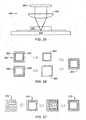
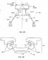
- Figures 1A and 1Billustrate two types of problems that may be encountered in imprint lithography.
- a wedge shaped imprinted layer 16results because that the template 12 is closer to the substrate 20 at one end of the imprinted layer 16.
- Figure 1Aillustrates the importance of maintaining template 12 and substrate 20 substantially parallel during pattern transfer.
- Figure 1Bshows the imprinted layer 16 being too thick. Both of these conditions are highly undesirable.
- Embodiments presented hereinprovide systems, processes and related devices which may eliminating the conditions illustrated in Figures 1A and 1B as well as other orientation problems associated with prior art lithography techniques.
- Figures 2A thru 2Eillustrate an embodiment of an imprint lithography process, denoted generally as 30.
- template 12is orientated in spaced relation to the substrate 20 so that a gap 31 is formed in the space separating template 12 and substrate 20.
- Surface 14 of template 12is treated with a thin layer 13 that lowers the template surface energy and assists in separation of template 12 from substrate 20.
- the manner of orientation and devices for controlling gap 31 between template 12 and substrate 20are discussed below.
- gap 31is filled with a substance 40 that conforms to the shape of treated surface 14.
- substance 40is dispensed upon substrate 20 prior to moving template 12 into a desired position relative to substrate 20.
- Substance 40forms an imprinted layer such as imprinted layer 16 shown in Figures 1A and 1B .
- substance 40may be a liquid so that it fills the space of gap 31 rather easily without the use of high temperatures and the gap can be closed without requiring high pressures. Further details regarding appropriate selections for substance 40 are discussed below.
- a curing agent 32is applied to the template 12 causing substance 40 to harden and assume the shape of the space defined by gap 31.
- desired features 44Figure 2D
- Transfer layer 18is provided directly on the upper surface of substrate 20. Transfer layer 18 facilitates the amplification of features transferred from the template 12 to generate high aspect ratio features.
- template 12is removed from substrate 20 leaving the desired features 44 thereon.
- the separation of template 12 from substrate 20must be done so that desired features 44 remain intact without shearing or tearing from the surface of the substrate 20.
- Embodiments presented hereinprovide a method and associated system for peeling and pulling (referred to herein as the "peel-and-pull" method) template 12 from substrate 20 following imprinting so that desired feature 44 remain intact.
- FIG. 2Efeatures 44 transferred from template 12 to substance 40 are amplified in vertical size by the action of the transfer layer 18 as is known in the use of bilayer resist processes.
- the resulting structureis further processed to complete the manufacturing process using well-known techniques.
- Figure 3summarizes an embodiment of an imprint lithography process, denoted generally as 50, in flow chart form.
- coarse orientation of a template and a substrateis performed so that a rough alignment of the template and substrate is achieved.
- An advantage of coarse orientation at step 52is that it may allow pre-calibration in a manufacturing environment, where numerous devices are to be manufactured, with efficiency and with high production yields.
- coarse alignmentis performed once on the first die and applied to all other dies during a single production run. In this way, production cycle times are reduced and yields are increased.
- a substanceis dispensed onto the substrate.
- the substancemay be a curable organosilicon solution or other organic liquid that becomes a solid when exposed to activating light.
- a liquidis used eliminates the need for high temperatures and high pressures associated with prior art lithography techniques.
- the spacing between the template and substrateis controlled so that a relatively uniform gap may be created between the two layers permitting the precise orientation required for successful imprinting.
- Embodiments presented hereinprovide a device and system for achieving the orientation (both course and fine) required at step 56.
- the gapis closed with fine orientation of the template about the substrate and the substance.
- the substanceis cured (step 59) resulting in a hardening of the substance into a form having the features of the template.
- the templateis separated from the substrate, step 60, resulting in features from the template being imprinted or transferred onto the substrate.
- the structureis etched, step 62, using a preliminary etch to remove residual material and a well-known oxygen etching technique to etch the transfer layer.
- a templateincorporates unpatterned regions i) in a plane with the template surface, ii) recessed in the template, iii) protrude from the template, or iv) a combination of the above.
- a templatemay be manufactured with protrusions, which may be rigid. Such protrusions provide a uniform spacer layer useful for particle tolerance and optical devices such as gratings, holograms, etc. Alternately, a template is manufactured with protrusions that are compressible.
- a templatemay have a rigid body supporting it via surface contact from: i) the sides, ii) the back, iii) the front or iv) a combination of the above.
- the template supporthas the advantage of limiting template deformation or distortion under applied pressure.
- a templateis coated in some regions with a reflective coating.
- the templateincorporates holes in the reflective coating such that light may pass into or through the template. Such coatings are useful in locating the template for overlay corrections using interferometry. Such coatings may also allow curing with a curing agent sources that illuminates through the sides of the template rather than the top.
- Exposure of the templatemay be performed: i) at normal incidences to the template, ii) at inclined angles to the template, or iii) through a side surface of the template.
- a template that is rigidis used in combination with a flexible substrate.
- the templatemay be manufactured using optical lithography, electron beamlithography, ion-beam lithography, x-ray lithography, extreme ultraviolet lithography, scanning probe lithography, focused ion beam milling, interferometric lithography, epitaxial growth, thin film deposition, chemical etch, plasma etch, ion milling, reactive ion etch or a combination of the above.
- the templateis formed on a substrate having a flat, topography.
- the templateis used with a substrate having a flat, topography.
- the substratemay contain a previously patterned topography and/or a film stack of multiple materials.
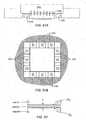
- a templatein an embodiment depicted in Figure 4 , includes a patterning region 401, an entrainment channel 402, and an edge 403.
- Template edge 403is utilized for holding the template within a template holder.
- Entrainment channel 402is configured to entrain excess fluid thereby preventing its spread to adjacent patterning areas, as discussed in more detail below.
- a patterned region of a templatemay be flat Such embodiments are useful for planarizing a substrate.
- the templatemay be manufactured with a multi-depth design. That is various features of the template are at different depths with relation to the surface of the template.
- entrainment channel 402may have a depth greater than patterning area 401.
- An advantage of such an embodimentis that accuracy in sensing the gap between the template and substrate is improved. Very small gaps (e.g., less than about 100nm) are difficult to sense; therefore, adding a step of a known depth to the template enables more accurate gap sensing.
- An advantage of a dual-depth designis that such enables using a standardized template holder to hold an imprint template of a given size which includes dies of various sizes.
- a third advantage of a dual-depth designenables using the peripheral region to hold the template.
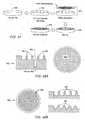
- a dual-depth imprint templatemay be fabricated using various methods.
- a single, thick substrate 601is formed with both a high-resolution, shallow-depth die pattern 602, and a low-resolution, large-depth peripheral pattern 603.
- a thin substrate 702e.g., quartz wafer
- Die pattern 701is then cut from substrate 702.
- Die pattern 701is then bonded to a thicker substrate 703, which has been sized to fit into an imprint template holder on an imprint machine. This bonding is preferably achieved using an adhesive 704 with an index of refraction of the curing agent (e.g., UV light) similar to that of the template material.
- the curing agente.g., UV light
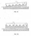
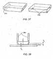
- FIG. 8A, 8B, and 8CAdditional imprint template designs are depicted in Figures 8A, 8B, and 8C and generally referenced by numerals 801, 802, and 803, respectively.
- Each of template designs 801, 802 and 803includes recessed regions which are used for gap measurement and or entrainment of excess fluid.
- a templateincludes a mechanism for controlling fluid spread that is based on the physical properties of the materials as well as geometry of the template.
- the amount of excess fluid which may be tolerated without causing loss of substrate areais limited by the surface energies of the various materials, the fluid density and template geometry.
- a relief structureis be used to entrain the excess fluid encompassing a region surrounding the desired molding or patterning area. This region is generally be referred to as the "kerf.”
- the relief structure in the kerfmay be recessed into the template surface using standard processing techniques used to construct the pattern or mold relief structure, as discussed above.
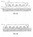
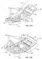
- Figure 9depicts an example of an imprint formed without accounting for material property changes 901, and an imprint formed accounting for changes in material properties 902.
- a templete with features having a substutially retangular profile 904are subject to deformations due to material shrinkage during curing.
- template featuresmay be provided with an angled profile 905.
- a durable templatemay be formed of a silicon or silicon dioxide substrate.
- suitable materialsmay include, but are not limited to: silicon germanium carbon, gallium nitride, silicon germanium, sapphire, gallium arsinide, epitaxial silicon, poly-silicon, gate oxide, quartz or combinations thereof.
- Templatesmay also include materials used to form detectable features, such as alignment markings.
- detectable featuresmay be formed of SiOx, where x is less than 2. In some embodiments x may be about 1.5. It is believed that this material may be opaque to visible light, but transparent to some activating light wavelengths.
- the durability of the templatemay be improved by treating the template to form a thin layer on the surface of the template.
- an alkylsilane, a fluoroalkylsilane, or a fluoroalkyltrichlorosilane layermay be formed on the surface, in particular tridecafluoro-1,1,2,2-tetrahydrooctyl trichlorosilane (C 6 F 13 C 2 H 4 SiCl 3 ) may be used.
- Such a treatmentforms a self-assembled monolayer (SAM) on the surface of the template.
- a surface treatment processmay be optimized to yield low surface energy coatings. Such a coating may be used in preparing imprint templates for imprint lithography.
- Treated templatesmay have desirable release characteristics relative to untreated templates. For example, newly-treated templates may posses surface free energies, ⁇ treated of about 1.4 ⁇ 10 -2 Nm (14 dynes/cm). Untreated template surfaces may posses surface free energies, ⁇ antreated about 6.5 ⁇ 10 -2 Nm (65 dynes/cm).
- a treatment procedure disclosed hereinmay yield films exhibiting a high level of durability. Durability may be highly desirable since it may lead to a template that may withstand numerous imprints in a manufacturing setting.
- a coating for the template surfacemay be formed using either a liquid-phase process or a vapor-phase process.
- a liquid-phase processthe substrate is immersed in a solution of precursor and solvent
- a precursoris delivered via an inert carrier gas. It may be difficult to obtain a purely anhydrous solvent for use in a liquid-phase treatments. Water in the bulk phase during treatment may result in clump deposition, which may adversely affect the final quality or coverage of the coating.
- the templatemay be brought to a desired reaction temperature via a temperature-controlled chuck.
- the precursormay then be fed into the reaction chamber for a prescribed time.
- Reaction parameterssuch as template temperature, precursor concentration, flow geometries, etc. may be tailored to the specific precursor and template substrate combination.
- substance 40may be a liquid so that it may fill the space of gap 31.
- substance 40may be a low viscosity liquid monomer solution.
- a suitable solutionhas a viscosity ranging from about 0.01 mPas (0.01cps) to about 100 mPas (100 cps) (measured at 25 degrees C).
- Low viscositiesare especially desirable for high-resolution (e.g., sub-100nm) structures.
- the viscosity of the solutionshould be at or below about 25 mPas (25 cps), or more preferably below about 5 mPas (5 cps) (measured at 25 degrees C).
- a suitable solutionincludes a mixture of 50% by weight n-butyl acrylate and 50% SIA 0210.0 (3-acryoloxypropyltristrimethylsiloxane)silane. To this solution is added a small percentage of a polymerization initiator (e.g., a photoinitiator). For example, a 3% by weight solution of a 1:1 Irg 819 and Irg 184 and 5% of SIB 1402.0 may be suitable. The viscosity of this mixture is about 1 mPas (1 cps).
- an imprint lithography systemincludes automatic fluid dispensing method and system for dispensing fluid on the surface of a substrate (e.g., a semiconductor wafer).
- the dispensing methoduses a modular automated fluid dispenser with one or more extended dispenser tips.
- the dispensing methoduses an X-Y stage to generate relative lateral motions between the dispenser tip and the substrate.
- the methodmay eliminate several problems with imprint lithography using low viscosity fluids. For example, the method may eliminate air bubble trapping and localized deformation of an imprinting area.
- Embodimentsmay also provide a way of achieving low imprinting pressures while spreading the fluid across the entire gap between the imprinting template and the substrate, without unnecessary wastage of excess fluid.
- a dispensed volumemay typically be less than about 130nl (nano-liter) for a 1 inch 2 imprint area.
- subsequent processesinvolves exposing the template and substrate assembly to a curing agent. Separation of the template from the substrate leaves a transferred image on top of the imprinted surface. The transferred image lies on a thin layer of remaining exposed material The remaining layer is referred to as a "base layer.”
- the base layershould be thin and uniform for a manufacturable imprint.
- Imprint processesmay involve high pressures and/or high temperatures applied at the template and substrate interface.
- high pressures and temperaturesshould be avoided.
- Embodiments disclosed hereinavoid the need for high temperature by using low viscosity photo-curable fluids.
- imprinting pressuresmay be minimized by reducing squeezing force required to spread the fluid across the entire imprinting area. Therefore, for the purpose of fluid based imprint lithography, a fluid dispense process should satisfy the following properties:
- relative motion between a displacement based fluid dispenser tip and a substrateare used to form a pattern with substantially continuous lines on an imprinting area. Size of the cross section of the line and the shape of the line are controlled by balancing rates of dispensing and relative motion.
- dispenser tipsare fixed near (e.g., on the order of tens of microns) the substrate.
- Two methods of forming a line patternare depicted in Figures 10A and 10B .
- the pattern depicted in Figures 10A and 10Bis a sinusoidal pattern; however, other patterns are possible. As depicted in Figures 10A and 10B continue line pattern may be drawn either using a single dispenser tip 1001 or multiple dispenser tips 1002.
- v da v a .
- the width of the initial line patternnormally depends on the tip size of a dispenser.
- the tip dispenseris fixed.
- a fluid dispensing controller 1111(as depicted in Figure 11 ) is used to control the volume of fluid dispensed (V d ) and the time taken to dispense the fluid (t d ). If V d and t d are fixed, increasing the length of the line leads to lower height of the cross section of the line patterned Increasing pattern length may be achieved by increasing the spatial frequency of the periodic patterns. Lower height of the pattern leads to a decrease in the amount of fluid to be displaced during imprint processes.
- a displacement based fluid delivery systemincludes: a fluid container 1101, an inlet tube 1102, an inlet valve 1103, an outlet valve 1104, a syringe 1105, a syringe actuator 1106, a dispenser tip 1107, an X stage actuator 1109, a Y stage actuator 1110, a dispenser controller 1111, an XY stage controller 1112, and a main control computer 1113.
- a suitable displacement based dispenseris available from the Hamilton Company
- Figure 12illustrates several undesirable fluid patterns or dispensing methods for low viscosity fluids. These dispensing patterns may lead to one or more problems, including: trapping air bubbles, localized deformations, and waste of fluid. For example, dispensing a single drop at the center of the imprinting area 1201, or dispensing irregular lines 1205 may lead to localized deformations of the template and/or substrate. Dispensing several drops 1202, or lines 1206 in a circumfrential pattern may lead to trapping of air bubbles. Other dispensing patterns with nearly closed circumfrencial patterns 1204 may similarly lead to air bubble trapping. Likewise, spraying or random placement of droplets 1203 may lead to trapping of air bubbles. Spin-coating a substrate with a low viscosity fluid may cause a "dewetting" problem due to the thin film instability. Dewetting may lead to formation of numerous small drops of fluid on the substrate, instead of a thin uniform layer of fluid.
- a fluid dispensing methodmultiple small drops of liquid that dispenses later are formed into a continuous body as they expand.
- Figures 13depicts the case of using five drops of liquid.
- five dropsare used only for the purpose of illustration.
- Other "open" patternssuch as a sinusoidal line, a 'W', or an 'X' may be implemented using this method.
- circular drops 1301become thinner and wider causing neighboring drops to merge together 1302. Therefore, even though the initial dispensing does not include a continuous form, the expanding liquid expels air from the gap between the template and substrate.
- a pattern effective for use in this methodshould be dispensed in such a way that as droplets expand, they do not trap any air between the template and substrate.
- micro-solenoid valveswith a pressure-supporting unit.
- Another type of the liquid dispensing actuatormay include a piezo-actuated dispenser.
- Advantages of a system with a micro-soleniod valves dispenser as compared to a displacement based fluid dispensermay include faster dispensing time and more accurate volume control. These advantages may be especially desirable for larger size imprints (e.g., several inches across).
- An embodiment which is only described for explanation as technical background of a system including micro-solenoid valvesis depicted in Figure 14 .
- the systemincludes: fluid container 1401, an inlet tube 1402, an inlet valve 1403, a pump 1404, an outlet valve 1405, a pump controller 1406, a micro-solenoid valve 1407, a micro-solenoid valve controller 1408, an X-Y stage 1409, an X-Y stage controller 1410, and a main computer 1412.
- a suitable micro-valve dispenser systemis available from the Lee Company
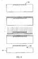
- FIG. 15AA dispensing pattern that is useful for large imprint areas (e.g., greater than several inch 2 ) is depicted in Figure 15A .
- parallel lines of fluid 1503are dispensed.
- Parallel lines of fluid 1503are expanded in such a way that air is expelled from the gap as template 1501 approach substrate 1502.
- template 1501closes the gap in an intentionally wedged configuration (as depicted in Figure 15B ). That is, the template/substrate gap is closed along lines 1503 (e.g., the wedge angle may be parallel to the lines 1503).
- the orientation error between the template and substrateis compensated for. This may be due to the hydraulic dynamics of the thin layer of fluid and compliance of the orientation stage.
- the lower portion of the templatecontacts the dispensed fluid earlier than other portions of the template.
- the imbalance of reaction forces between the lower and higher portions of the templateincreases. This imbalance of forces leads to a correcting motion for the template and substrate, bring them into a substantially parallel relationship.
- the systemmay include a high resolution X-Y translation stage.
- the systemmay provide a pre-calibration stage for performing a preliminary and course alignment operation between the template and substrate surface to bring the relative alignment to within the motion range of a fine movement orientation stage. This pre-calibration stage may be required only when a new template is installed into the apparatus (also sometimes known as a stepper).
- the pre-calibration stagemay consist of a base plate, a flexure component, and a plurality of micrometers or high resolution actuators coupling the base plate and the flexure component.
- Figure 16depicts an embodiment of an X-Y translation stage in an assembled configuration, and generally referenced by numeral 1600.
- the overall footprintmay be less than about 50 x 50cm (20 inches by 20 inches) and the height may be about 15 cm (5 inches) (including a wafer chuck).
- Such an embodimentprovides X and Y-axis translation ranges of motion of about 30 cm (12 inches).
- stage 1700may have a foot print of about 73 x 73 cm (29 inches by 29 inches) and a height of about 24 cm (9.5 inches) (including a wafer chuck). Stages 1600 and 1700 differ mainly in that additional linkages 1701 are oriented vertically, thereby providing additional load bearing support for the translation stage.
- Both X-Y stage 1600 and X-Y stage 1700are flexure based systems. Flexures are widely used in precision machines since they may offer frictionless, particle-free and low maintenance operation. Flexures may also provide extremely high resolution. However, most flexure based systems may possess limited ranges of motion (e.g., sub mm range of motion). Embodiments disclosed herein may have a range of motion of more than 30cm (12 inches). It is believed that such stages may be cost-effective for lithographic applications, particularly in vacuum. Further, for imprint lithography techniques, the presence of imprint forces may give embodiments presented herein significant advantages.
- an X-Y stagemay include two types of components: actuation components and load-carrying components.
- Lead screw assembly mechanismshave been widely used where the positioning accuracy is not a very significant factor.
- ball screw assemblieshave been used for both the actuating and load-carrying components. Both of these designs may be prone to problems of backlash and stiction. Further, the need for lubrication may make these designs undesirable for use in vacuum or in particle-sensitive applications (e.g., imprint lithography).
- Air bearingsmay substantially eliminate problems of stiction and backlash. However, air bearings may provide limited load bearing capacities. Additionally, air bearings may be unsuitable for use in vacuum environments.
- Figure 18shows a schematic of portion of a basic linkage 1800.
- Link 1 1804 and link 3 1805may be of the same length.
- all of the joints in linkage 1800rotate by the same absolute angle. It should be noted that the motion range may be independent of the length of link 2 1803. Due to kinematic constraints, link 21803 may remain parallel to a line between joint 1 1806 and joint 41807.
- the minimum link length for a 12 inch motion rangeis 6 inches.
- Figure 19depicts an embodiment which is only described for explanation as technological background of a basic linkage similar to linkage 1800, but with the addition of two cylindrical disks 1902.
- a kinematic studyshows that if joint 2 1904 and joint 3 1905 of Figure 19 rotate in opposite directions by the same angle, the stage may generate a pure translational motion along the X axis.
- the resulting rolling contactmay rotate link 1 1908 and link 2 1906 in opposite directions.
- no additional joints or bearingsmay be required since cylindrical discs 1902 may be coupled to links 1908 and 1906.
- an appropriate pre-loadmay be applied between the two disks.
- disks 1902are not depicted in relation to X-Y stages 1600, and 1700, disks 1902 may be present in some embodiments.
- Links 1602 and 1601 in Fig. 16may correspond to links 1908 and 1906 of Fig. 19 .
- disks 1902may be present at location 1603 (as well as other locations not visible in the Figure 16 ).
- disks 1902may be present at location 1702 (as well as other locations not visible in Figure 17 )
- two linear servo motorsmay be suitable.
- One linear servo motormay serve each translation axis.
- Suitable linear servo motorsis available from the Trilogy Systems Corporation.
- An advantage of such linear servo motorsis the absence of frictional contact.
- Another advantage of such linear servo motorsis the fact that they readily produce actuation forces greater than about 100 pounds.
- load-bearingare provided by additional linkages 1701. Therefore, actuation components provide only translational motion control in the X and Y directions.
- laser interferometersmay provide a feedback signal to control X and Y positioning of the X-Y stage. It is believed that laser interferometry may provide nm level positioning control.
- Placement errorscan be compensated using laser interferometers and high resolution X-Y stages (such as X-Y stage 1700, depicted in Fig. 17 ). If the orientation alignments between the template and substrate are independent from X-Y motions the placement error may need to be compensated only once for an entire substrate wafer (i.e., "global overlay"). If orientation alignments between the template and substrate are coupled with X-Y motions and/or excessive local orientation variations on substrate exist, then X-Y position changes of the template relative to the substrate may need to be compensated for (i.e., field-to-field overlay). Overlay alignment issues are further discussed with regard the overlay alignment section. Figures 21 and 22 provide global and field-to-field overlay error compensation algorithms, respectively.
- orientation of template and substrateis achieved by a pre-calibration stage (automatically, using actuators or manual, using micrometers) and a fine orientation stage, which may be active or passive. Either or both of these stages includes other mechanisms, but flexure-based mechanisms may be preferred in order to avoid particles.
- the calibration stagemay be mounted to a frame, and the fine orientation stage may be mounted to the pre-calibration stage. Such an embodiment may thereby form a serial mechanical arrangement.
- a fine orientation stagemay include one or more passive compliant members.
- a "passive compliant member”may generally refer to a member that gets its motion from compliance. That is, motion may be activated by direct or indirect contact with the liquid. If the fine orientation stage is passive, then it may be designed to have the most dominant compliance about two orientation axes. The two orientation axes may be orthogonal and may lie on the template lower surface (as described with referenced to Figure 43 ). The two orthogonal torsional compliance values may typically be the same for a square template.
- the fine orientation stagemay be designed such that when the template is non-parallel with respect to the substrate, as it makes contact with the liquid, the resulting uneven liquid pressure may rapidly correct the orientation error. In an embodiment, the correction may be affected with minimal, or no overshoot. Further, a fine orientation stage as described above may hold the substantially parallel orientation between the templates and substrate for a sufficiently long period to allow curing of the liquid.
- a fine orientation stagemay include one or more actuators.
- piezo actuatorsas described with reference to Figure 46
- the effective passive compliance of the fine orientation stage coupled with the pre-calibration stageshould still be substantially tosional about the two orientation axes.
- the geometric and material parameters of all the structural and active elements togethermay contribute to this effective passive stiffness.
- piezo actuatorsmay also be compliant in tension and compression.
- the geometric and material parametersmay be synthesized to obtain the desired torsional compliance about the two orthogonal orientation axes.
- a simple approach to this synthesismay be to make the compliance of the actuators along their actuation direction in the fine orientation stage higher than the structural compliances in the rest of the stage system. This may provide passive self-correction capability when a non-parallel template comes into contact with the liquid on the substrate. Further, this compliance should be chosen to allow for rapid correct orientation errors, with mininimal or no overshoot.
- the fine orientation stagemay hold the substantially parallel orientation between the template and substrate for sufficiently long period to allow curing of the liquid.
- Overlay alignment schemesmay include measurement of alignment errors followed by compensation of these errors to achieve accurate alignment of an imprint template, and a desired imprint location on a substrate.
- the measurement techniques used in proximity lithography, x-ray lithography, and photolithographye.g., laser interferometry, capacitance sensing, automated image processing of overlay marks on the mask and substrate, etc
- photolithographymay be adapted for the imprint lithography process with appropriate modifications.
- Types of overlay errors for lithography processesmay include placement error, theta error, magnification error, and mask distortion error.
- An advantage of embodiments disclosed hereinis that mask distortion errors are not present because the disclosed processes may operate at relatively low temperatures (e.g., room temperature) and low pressures. Therefore, these embodiments do not induce significant distortion.
- these embodimentsuse templates that are made of a relatively thick substrate. This lead to much smaller mask (or template) distortion errors as compared to other lithography processes where masks are made of relatively thin substrates.
- the entire area of the templates for imprint lithography processesmay be transparent to the curing agent (e.g., UV light), which minimizes heating due to absorption of energy from the curing agent. The reduced heating minimizes the occurrence of heat-induced distortions compared to photolithography processes where a significant portion of the bottom surface of a mask may be opaque due to the presence of a metallic coating.
- Placement errormay generally refer to X-Y positioning errors between a template and substrate (that is, translation along the X and/or Y-axis).
- Theta errormay generally refer to the relative orientation error about Z-axis. (that is, rotation about the Z-axis).
- Magnification errormay generally refer to thermal or material induced shrinkage or expansion of the imprinted area as compared to the original patterned area on the template.
- orientation alignment for gap control purposes between a template and substrate corresponding to the angles ⁇ and ⁇ in Figure 23may need to be performed frequently if excessive field-to-field surface variations exist on the substrate. In generally, it is desirable for the variation across an imprinting area to be smaller than about one-half of the imprinted feature height. If orientation alignments are coupled with the X-Y positioning of the template and substrate, field-to-field placement error compensations may be necessary. However, embodiments of orientation stages that may perform orientation alignment without inducing placement errors are presented herein.
- Photolithography processes that use a focusing lens systemmay position the mask and substrate such that it may be possible to locate the images of two alignment marks (one on the mask and the other on the substrate) onto the same focal plane. Alignment errors may be induced by looking at the relative positioning of these alignment marks.
- the template and substratemaintain a relatively small gap (of the order of micro meters or less) during the overlay error measurement. Therefore, overlay error measurement tools may need to focus two overlay marks from different planes onto the same focal plane.
- Such a requirementmay not be critical for devices with features that are relatively large (e.g., about 0.5 ⁇ m).
- the images of the two overlay marksshould to be captured on the same focal plane in order to achieve high resolution overlay error measurements.
- overlay error measurement and error compensation methods for imprint lithography processesshould to satisfy the following requirements:
- the first requirement presented abovecan be satisfied by i) moving an optical imaging tool up and down (as in US Patent 5,204,739 ) or ii) using illumination sources with two different wavelengths.
- knowledge of the gap measurement between the template and the substrateis useful, especially for the second method.
- the gap between the template and substratemay be measured using one of existing non-contact film thickness measurement tools including broad-band interferometry, laser interferometry and capacitance sensors.
- Figure 24illustrates the positions of template 2400, substrate 2401, fluid 2403, gap 2405 and overlay error measurement tools 2402.
- the height of a measuring toolis adjusted 2406 according to the gap information to acquire two overlay marks on the same imaging plane.
- an image storing 2403 deviceis required.
- the positioning devices of the template and waferis vibrationally isolated from the up and down motions of the measuring device 2402. Further, when scanning motions in X-Y directions between the template and substrate are needed for high resolution overlay alignment, this approach may not produce continuous images of the overlay marks. Therefore, this approach is adapted for relatively low-resolution overlay alignment schemes for the imprint lithography process.
- Figure 25illustrates as technological background an apparatus for focusing two alignment marks from different planes onto a single focal plane.
- Apparatus 2500uses the change of focal length resulting from light with distinct wavelengths being used as the illumination sources.
- Apparatus 2500may include an image storage device 2503, and illumination source (not shown), and a focusing device 2505
- Light with distinct wavelengthsmay be generated either by using individual light sources or by using a single broad band light source and inserting optical band-pass filters between the imaging plane and the alignment marks.
- a different set of two wavelengthsmay be selected to adjust the focal lengths.
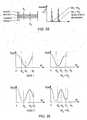
- each overlay markmay produce two images on the imaging plane as depicted in Figure 26 .
- a first image 2601may be a clearly focused image.
- a second image 2602may be an out-of-focus image. In order to eliminate each out-of-focus image, several methods may be used.
- a first methodunder illumination with a first wavelength of light, two images are received by an imaging array (e.g., a CCD array). Images which are received are depicted in Figure 26 and generally referenced by numeral 2604. Image 2602 correponds to an overlay alignment mark on the substrate. Image 2601 corresponds to an overlay alignment mark on the template. When image 2602 is focused, image 2601 may be out of focus, and visa-versa. In an embodiment, an image processing technique is used to erase geometric data corresponding to pixels associated with image 2602. Thus, the out of focus image of the substrate mark is eliminated, leaving image 2603. Using the same procedure and a second wavelength of light, image 2605 and 2606 are formed on the imaging array. The procedure eliminates out of focus image 2606. Thus image 2605 remains. The two remaining focused images 2601 and 2605 are then combined onto a single imaging plane 2603 for making overlay error measurements.
- an imaging arraye.g., a CCD array
- a second methodutilizes two coplanar polarizing arrays, as depicted in Figure 27 , and polarized illumination sources.
- Figure 27illustrates overlay marks 2701 and orthogonally polarized arrays 2702.
- Polarizing arrays 2702may be made on the template surface or may be placed above it Under two polarized illumination sources, only focused images 2703 (each corresponding to a distinct wavelength and polarization) appear on the imaging plane. Thus, out of focus images are filtered out by polarizing arrays 2702.
- An advantage of this methodis that it does not require an image processing technique to eliminate out-focused images.
- Moire pattern based overlay measurementhas been used for optical lithography processes.
- For imprint lithography processeswhere two layers of Moire patterns are not on the same plane but still overlapped in the imaging array, acquiring two individual focused images may be difficult to achieve.
- carefully controlling the gap between the template and substrate within the depth of focus of the optical measurement tool and without direct contact between the template and substratemay allow two layers of Moire patterns to be simultaneously acquired with minimal focusing problems. It is believed that other standard overlay schemes based on the Moire patterns may be directly implemented to imprint lithography process.
- Placement errorsmay be compensated for using capacitance sensors or laser interferometers, and high resolution X-Y stages.
- placement errormay need to be compensated for only once for an entire substrate (e.g., a semiconductor wafer).
- Such a methodmay be referred to as a "global overlay.”
- X-Y position change of the templatemay be compensated for using capacitance sensors and/or laser interferometers.
- Such a methodmay be referred to as a "field-to-field overlay.”
- Figures 28 and 29depict suitable sensor implementations.
- Figure 28depicts an embodiment of a capacitance sencing system which is described for explanation as technological background, only.
- a capacitance sensing systemincludes capacitance sensors 2801, a conductive coating 2802, on a template 2803. Thus, by sensing differences in capacitance, the location of template 2803 is determined.
- Figure 29depicts an embodiment of a laser interferometer system including reflective coating 2901, laser signal 2902, received 2903. Laser signals received by receiver 2903 is used to determine the location of template 2904.
- magnification errorif any exists, is compensated for by carefully controlling the temperature of the substrate and the template. Using the difference of the thermal expansion properties of the substrate and template, the size of pre-existing patterned areas on the substrate are adjusted to that of a new template. However, it is believed that the magnification error is much smaller in magnitude than placement error or theta error when an imprint lithography process is conducted at room temperature and low pressures.
- the theta errormay be compensated for using a theta stage that has been widely used for photolithography processes.
- Theta errormay be compensated for by using two separate alignment marks that are seperated by a sufficiently large distance to provide a high resolution theta error estimate.
- the theta errormay be compensated for when the template is positioned a few microns apart from the substrate. Therefore, no shearing of existing patterns occurs.
- the template overlay marksmay typically not include opaque lines. Rather, the template overlay marks may be topographical features of the template surface. In some embodiment, the marks may be made of the same material as the template.
- UV curable liquidsmay tend to have refractive indices that are similar to those of the template materials (e.g., quartz). Therefore, when the UV curable liquid fills the gap between the template and the substrate, template overlay marks may become very difficult to recognize. If the template overlay marks are made with an opaque material (e.g., chromium), the UV curable liquid below the overlay marks may not be properly exposed to the UV light, which is highly undesirable.
- a first methoduses an accurate liquid dispensing system along with high-resolution gap controlling stages. Suitable liquid dispensing systems and the gap controlling stages are disclosed herein.
- three steps of an overlay alignmentare depicted in Figure 30 .
- the locations of the overlay marks and the patterns of the fluid depicted in Figure 30are only for the purpose of illustration and should not be construed in a limiting sense.
- Various other overlay marks, overlay mark locations, and/or liquid dispense patternsare also possible.
- a liquid 3003may be dispensed onto substrate 3002.
- step 3004using the high-resolution orientation stage, the gap between template 3005 and substrate 3002 is carefully controlled so that the dispensed fluid 3003 does not fill the gap between the template and substrate completely. It is believed that at step 3004, the gap may be only slightly larger than the final imprinting gap. Since most of the gap is filled with the fluid, overlay correction can be performed as if the gap were completely filled with the fluid. Upon the completion of the overlay correction, the gap is closed to a final imprinting gap (step 3006). This may enable spreading of the liquid into the remaining imprint area. Since the gap change between steps 3004 and 3006 may be very small (e.g., about 10nm), the gap closing motion is unlikely to cause any significant overlay error.
- the gap change between steps 3004 and 3006may be very small (e.g., about 10nm), the gap closing motion is unlikely to cause any significant overlay error.
- a second methodmay be to make special overlay marks on the template that may be seen by the overlay measurement tool but may not be opaque to the curing agent (e.g., UV light).
- An embodiment of this approachis illustrated in Figure 31 .
- overlay marks 3102 on the templatemay be formed of fine polarizing lines 3101.
- suitable fine polarizing linesmay have a width about 1 ⁇ 2 to 1 ⁇ 4 of the wavelength of activating light used as the curing agent.
- the line width of polarizing lines 3101should be small enough so that activating light passing between two lines is diffracted sufficiently to cause curing of all the liquid below the lines.
- the activating lightmay be polarized according to the polarization of overlay marks 3102.
- Polarizing the activating lightmay provide a relatively uniform exposure to all the template regions including regions having overlay marks 3102.
- Light used to locate overlay marks 3102 on the templatemay be broadband light or a specific wavelength that may not cure the liquid material. This light need not be polarized.
- Polarized lines 3101may be substantially opaque to the measuring light, thus making the overlay marks visible using established overlay error measuring tools. Fine polarized overlay marks may be fabricated on the template using existing techniques, such as electron beam lithography.
- overlay marksmay be formed of a different material than the template.
- a material selected to form the template overlay marksmay be substantially opaque to visible light, but transparent to activating light used as the curing agent (e.g., UV light).
- the curing agente.g., UV light
- SiOx where X is less than 2may form such a material.
- structures formed of SiOx where X is about 1.5may be substantially opaque to visible light, but transparent to UV light.
- Figure 32depicts an assembly of a system, denoted generally as 100, for calibrating and orienting a template, such as template 12, about a substrate to be imprinted, such as substrate 20.
- System 100may be utilized in a machine, such as a stepper, for mass fabrication of devices in a production environment using imprint lithography processes as described herein. As shown, system 100 may be mounted to a top frame 110 which may provide support for a housing 120. Housing 120 may contain the pre calibration stage for course alignment of a template 150 about a substrate (not shown in Figure 32 ).
- Housing 120is coupled to a middle frame 114 with guide shafts 112a, 112b attached to middle frame 114 opposite housing 120.
- guide shafts 112a, 112battached to middle frame 114 opposite housing 120.
- three (3) guide shaftsare used (the back guide shaft is not visible in Figure 32 ) to provide a support for housing 120 as it slides up and down during vertical translation of template 150.
- Sliders 116a and 116b attached to corresponding guide shafts 112a, 112b about middle frame 114facilitate this up and down motion of housing 120.
- System 100includes a disk-shaped base plate 122 attached to the bottom portion of housing 120.
- Base plate 122is coupled to a disk-shaped flexure ring 124.
- Flexure ring 124supports the lower placed orientation stage included of first flexure member 126 and second flexure member 128.
- the operation and configuration of the flexure members 126, 128are discussed in detail below.
- the second flexure member 128includes a template support 130, which holds template 150 in place during the imprinting process.
- template 150may include a piece of quartz with desired features imprinted on it Template 150 may also include other substances according to well-known methods.
- actuators 134a, 134b, 134care fixed within housing 120 and operable coupled to base plate 122 and flexure ring 124. In operation, actuators 134a, 134b, 134c are controlled such that motion of the flexure ring 124 is achieved. Motion of the actuators allows for coarse pre-calibration.
- actuators 134a,134b, 134cinclude high resolution actuators. In such embodiments, the acuators are be equally spaced aroung housing 120. Such an embodiment permits very precise translation of the ring 124 in the vertical direction to control the gap accurately.
- the system 100is be capable of achieving coarse orientation alignment and precise gap control of template 150 with respect to a substrate to be imprinted.
- System 100includes a mechanism that enables precise control of template 150 so that precise orientation alignment may be achieved and a uniform gap may be maintained by the template with respect to a substrate surface. Additionally, system 100 provides a way of separating template 150 from the surface of the substrate following imprinting without shearing of features from the substrate surface. Precise alignment and gap control are facilitated by the configuration of the first and second flexure members, 126 and 128, respectively.
- template 5102is held in place using a separated, fixed supporting plate 5101 that is transparent to the curing agent as depicted in Figure 51 . While supporting plate 5101 behind template 5102 supports the imprinting force, applying vacuum between fixed supporting plate 5101 and template 5102 may supports the separation force.
- piezo actuators 5103is used. The lateral supporting forces are carefully controlled by using piezo actuators 5103. This design also provide the magnification and distortion correction capability for layer-to-layer alignment in imprint lithography processes. Distortion correction is very important to overcome stitching and placement errors present in the template structures made by electron beam lithography, and to compensate for distortion in the previous structures present on the substrate.
- Magnification correctiononly required one piezo actuator on each side of the template (i.e. total of 4 piezo actuators for a four sided template).
- the actuatorsis connected to the template surface in such a way that a uniform force may be applied on the entire surface.
- Distortion correctionrequires several independent piezo actuators that apply independently controlled forces on each side of the template. Depending on the level of distortion control required, the number of independent piezo actuators is specified. More piezo actuators provide better control of distortion.
- the magnification and distortion error correctionshould be completed prior to the use of vacuum to constrain the top surface of the template. This is because magnification and distortion correction may be properly controlled only if both the top and bottom surfaces of the template are unconstrained.
- the template holder system of Figure 51has a mechanical design that causes obstruction of the curing agent to a portion of the area under template 5102. This may be undesirable because a portion of the liquid below template 5102 may not cure. This liquid may stick to the template causing problems with further use of the template.
- This problem with the template holdermay be avoided by incorporating a set of mirrors into the template holder to divert the obstructed curing agent in such a way that curing agent directed to the region below one edge of template 5102 may be bent to cure an obstructed portion below the other edge of template 5102.
- high resolution gap sensingmay be achieved by designing the template such that the minimum gap between the substrate and template falls within a sensing technique's usable range.
- the gap being measuredmay be manipulated independently of the actual patterned surface. This allows gap control to be performed within the useful range of the sensing technique. For example, if a spectral reflectivity analysis technique with a useful sensing range of about 150nm to 20 microns is to be used to analyze the gap, then the template may have feature patterned into the template with a depth of about 150 nm or greater. This ensures that the minimum gap that to be sensed is greater than 150mm.
- the fluidmay be expelled from the gap between the substrate and the template.
- the gap between the substrate and the templatemay approach a lower practical limit when the viscous forces approach equilibrium conditions with the applied compressive force. This may occur when the surface of the template is in close proximity to the substrate.
- this regimemay be at a gap height of about 100nm for a 1 mPas (1 cP) fluid when 14kPa is applied for 1 sec to a template with a radius of 1cm.
- the gapmay be self-limiting provided a uniform and parallel gap is maintained.
- a fairly predictable amount of fluidmay be expelled (or entrained).
- the volume of fluid entrainedmay be predictable based on careful fluid dynamic and surface phenomena calculations.
- a template manufactured with reticle fabrication techniquesmay be used in combination with gap sensing technology such as i) single wavelength interferometry, ii) multi-wavelength interferometry, iii) ellipsometry, iv) capacitance sensors, or v) pressure sensors.
- a method of detecting gap between template and substrateis used in computing thickness of films on the substrate.
- a description of a technique based on Fast Fourier Transform (FFT) of reflective data obtained from a broad-band spectrometeris disclosed herein.
- FFTFast Fourier Transform
- This techniquemay be used for measuring the gap between the template and the substrate, as well as for measing film thickness.
- the techniquemay provide an average thickness of each thin film and its thickness variations.
- the average gap and orientation information between two surfaces in close proximity, such as the template-substrate for imprint lithography processesmay be acquired by measuring gaps at a minimum of three distinct points through one of the surfaces.
- a gap measurement processmay be based the combination of the broad-band interferometry and Fast Fourier Transform (FFT).
- FFTFast Fourier Transform
- FIG 34depicts an embodiment of a process flow of film thickness or gap, measurement via a FFT process of a reflectivity signal.
- locations of peaks in FFT processmay correspond to linear combinations of each film thickness.
- a two-layer filmmay lead to two distinct peak locations in a FFT analysis.
- Figure 35depicts a method of determining the thickness of two films based on two peak locations.
- Embodiments presented hereinmay enable measuring a gap or film thickness even when the oscillation of the reflectivity data includes less than one full period within the measuring wavenumber range. In such a case, FFT may result in an inaccurate peak location.
- the wavenumber range ( ⁇ w) of typical spectrometersmay be larger than w,.
- the film thicknesscan be computed as follows:
- a practical configuration of the measurement toolmay include a broad-band light source, a spectrometer with fiber optics, a data aquisistion board, and a processing computer.
- Several existing signal processing techniquesmay improve the sensitivity of the FFT data. For example, techniques including but not limited to: filtering, magnification, increased number of data points, different range of wavelengths, etc., may be utilized with gap or film thickness measurement methods disclosed herein.
- Embodiments disclosed hereininclude a high precision gap and orientation measurement method between two flats (e.g., a template and a substrate). Gap and orientation measurement methods presented here include use of broad-band interferometry and fringe based interferometry.
- a method disclosed herein which uses broad-band interferometrymay overcome a disadvantage of broad-band interferometer, namely its inability to accurately measure gaps smaller than about 1/4 of the mean wavelength of the broad-band signal.
- Interference fringe based interferometrymay be used for sensing errors in the orientation of the template soon after it is installed.
- Imprint lithography processesmay be implemented to manufacture single and multi layer devices.
- Single layer devicessuch as micron size optical mirrors, high resolution light filters, light guides may be manufactured by forming a thin layer of material in certain geometric shapes on substrates.
- the imprinted layer thickness of some of these devicesmay be less than 1/4 of the mean wavelength of a broad-band signal, and may be uniform across an active area.
- a disadvantage of broad-band interferometermay be that it may be unable to accurately measure gaps smaller than about 1/4 of the mean wavelength of the broad-band signal (e.g., about 180nm).
- micrometer size stepswhich may be measured accurately, may be etched into the surface of the template.
- stepsmay be etched down in the forms of continuous lines 3701 or multiple isolated dots 3702 where measurements may be made.
- Isolated dots 3702may be preferable from the point of view of maximizing the useful active area on the template.
- a broad-band interferometermay measure the gap accurately without suffering from minimum gap measurement problems.
- Figure 38depicts a schematic of the gap measurement described here. Probes 3801 may also be used in an inclined configuration, such as depicted in Figure 39 . If more than three probes are used, the gap measurement accuracy may be improved by using the redundant information. For simplicity's sake, the ensuing description assumes the use of three probes.
- the step size, h s AC2is magnified for the purpose of illustration.
- the relative orientation of the template with respect to the substratemay be expressed as an unit vector (n) that is normal to the template surface with respect to a frame whose x-y axes lie on the top surface of the substrate.
- Measured gaps and orientationsmay be used as feedback information to imprinting actuators.
- the size of the measuring broad-band interferometric beammay be as small as about 75 ⁇ m.
- Figure 40depicts a schematic of multi-layer materials on substrates.
- substrate 4001has layers 4002, and 4003, and fluid 4005 between substrate 4001 and template 4004. These material layers may be used to transfer multiple patterns, one by one vertically, onto the substrate surface. Each thickness may be uniform at the clear area where a gap measurement may be made using light beams 4006. It has been shown that using broad-band interferometry, the thickness of a top layer may be measured accurately in the presence of multi-layer films. When the optical properties and thicknesses of lower layer films are known accurately, the gap and orientation information between the template and substrate surface (or metal deposited surfaces for multi-layer devices) may be obtained by measuring the top layer thickness. The thickness of each layer may be measured using the same sensing measurement probes.
- the orientation error between the template 4102 and substrate 4103may be measured via an interference fringe pattern at the template and substrate interface as depicted in Figure 41 .
- the interference fringe patternmay appear as parallel dark and light bands 4101.
- Orientation calibrationmay be performed using a pre-calibration stage as disclosed herein. Differential micrometers may be used to adjust the relative orientation of the template with respect to the substrate surface. Using this approach, if no interference fringe band is present, the orientation error may be corrected to be less than 1 ⁇ 4 of the wavelength of light source used.
- the first flexure member 126includes a plurality of flexure joints 160 coupled to corresponding rigid bodies 164, 166. Flexure joints 160 and rigid bodies 164, and 166 may form part of arms 172, 174 extending from a frame 170. Flexure frame 170 may have an opening 182, which may permit the penetration of a curing agent (e.g., UV light) to reach the template 150 when held in support 130.
- a curing agente.g., UV light
- four (4) flexure joints 160provide motion of the flexure member 126 about a first orientation axis 180.
- Frame 170 of first flexure member 126may provide a coupling mechanism for joining with second flexure member 128 as illustrated in Figure 43 .
- second flexure member 128includes a pair of arms 202, 204 extending from a frame 206.
- Arms 202 and 204may include flexure joints 162 and corresponding rigid bodies 208, 210.
- Rigid bodies 208 and 210may be adapted to cause motion of flexure member 128 about a second orientation axis 200.
- a template support 130may be integrated with frame 206 of the second flexure member 128.
- frame 206may have an opening 212 permitting a curing agent to reach template 150 which may be held by support 130.
- first flexure member 126 and second flexure member 128are joined as shown in Figure 43 to form orientation stage 250.
- Braces 220, 222are provided in order to facilitate joining of the two pieces such that the first orientation axis 180 and second orientation axis 200 are substantially orthogonal to each other.
- first orientation axis 180 and second orientationintersect at a pivot point 252 at approximately the template substrate interface 254.
- the fact that first orientation axis 180 and second orientation axis 200 are orthogonal and lie on interface 254provides fine alignment and gap control. Specifically, with this arrangement, a decoupling of orientation alignment from layer-to-layer overlay alignment is achieved.
- first orientation axis 180 and second orientation axis 200provides an orientation stage 250 that may be used to separate the template 150 from a substrate without shearing of desired features. Thus, features transferred from the template 150 may remain intact on the substrate.
- flexure joints 160 and 162are notched shaped to provide motion of rigid bodies 164, 166,208, 210 about pivot axes that are located along the thinnest cross section of the notches.
- This configurationprovides two (2) flexure-based sub-systems for a fine decoupled orientation stage 250 having decoupled compliant motion axes 180, 200.
- Flexure members 126, 128are assembled via mating of surfaces such that motion of template 150 may occur about pivot point 252 substantially eliminating "swinging" and other motions that could shear imprinted features from the substrate.
- orientation stage 250precisely moves the template 150 about a pivot point 252; thereby, eliminates shearing of desired features from a substrate following imprint lithography.
- a Z-translation stagecontrols the distance between template 150 and the substrate without providing orientation alignment.
- a pre-calibration stage 260performs a preliminary alignment operation between template 150 and the substrate surfaces to bring the relative alignment to within the motion range limits of orientation stage 250. In certain embodiments, pre-calibration is required only when a new template is installed into the machine.
- Flexure model 300may include four (4) parallel joints : joints 1, 2, 3 and 4, that provide a four-bar-linkage system in its nominal and rotated configurations.
- Line 310passes though joints 1 and 2.
- Line 312passes through joints 3 and 4.
- Angles ⁇ 1 and ⁇ 2may be selected so that the compliant alignment (or orientation axis) axis lies substantially on the template-wafer interface 254.
- rigid body 314 between Joints 2 and 3may rotate about an axis depicted by Point C.
- Rigid body 314is representative of rigid bodies 170 and 206 of flexure members 126 and 128.
- Mounting a second flexure component orthogonally onto the first oneprovides a device with two decoupled orientation axes that are orthogonal to each other and lie on the template-substrate interface 254.
- the flexure componentsmay be adapted to have openings to allow a curing agent (e.g., UV light) to pass through the template 150.
- the orientation stage 250may be capable of fine alignment and precise motion of template 150 with respect to a substrate. Ideally, the orientation adjustment may lead to negligible lateral motion at the interface and negligible twisting motion about the normal to the interface surface due to selectively constrained high structural stiffness.
- Another advantage of flexure members 126, 128 with flexure joints 160, 162is that they do not generate particles as frictional joints may. This is an important factor in the success of an imprint lithography process as particles may be particularly harmful to such processes.
- a gap sensing methodcapable of measuring small gaps of the order of 500nm or less between the template and substrate.
- Such a gap sensing methodmay require a resolution of about 50 nanometers, or less.
- such gap sensingmay be provided in real-time. Providing gap sensing in real-time may allow the gap sensing to be used to generate a feedback signal to actively control the actuators.
- Figure 46depicts a flexure member, denoted generally as 400, including piezo actuators.
- Flexure member 400may be combined with a second flexure member to form an active orientation stage.
- Flexure member 400generates pure tilting motions with no lateral motions at the template-substrate interface.
- a single overlay alignment stepallows the imprinting of a layer on an entire semiconductor wafer. This is in contrast to overlay alignment with coupled motions between the orientation and lateral motions.
- Such overlay alignment stepslead to disturbances in X-Y alignment, and therefore require a complicated field-to-field overlay control loop to ensure proper alignment
- flexure member 250may possess high stiffness in the directions where side motions or rotations are undesirable and lower stiffness in directions where necessary orientation motions are desirable. Such an embodiment provides a selectively compliant device. That is, flexure member 250 supports relatively high loads while achieving proper orientation kinematics between the template and the substrate.
- Template 150may be made from optical flat glass using electron beam lithography to ensure that it is substantially flat on the bottom.
- the substratee.g., a semiconductor wafer
- Vacuum chuck 478(as shown in Figure 47 ), may eliminate variations across a surface of the substrate that may occur during imprinting.
- Vacuum chuck 478serves two primary purposes. First, vacuum chuck 478 is utilized to hold the substrate in place during imprinting and to ensure that the substrate stays flat during the imprinting process. Additionally, vacuum chuck 478 engages that no particles are present on the back of the substrate during processing. This may be especially important to imprint lithography, as particles may create problems that ruin the device and decrease production yields.
- Figure 48A and 48Billustrate variations of a vacuum chuck suitable for these purposes according to two embodiments.
- a pin-type vacuum chuck 450is shown as having a large number of pins 452. It is believed that vacuum chuck 450 eliminates "potato chip" effects as well as other deflections on the substrate during processing.
- a vacuum channel 454is provided as a means of applying vacuum to the substrate to keep it in place. The spacing between the pins 452 is maintained such that the substrate will not bow substantially from the force applied through vacuum channel 454. At the same time, the tips of pins 452 are small enough to reduce the chance of particles settling on top of them.
- Figure 48Bdepicts a groove-type vacuum chuck 460 with a plurality of grooves 462 across its surface.
- Grooves 462may perform a similar function to pins 454 of the pin-type vacuum chuck 450.
- grooves 462take on either a wall shape 464 or a smooth curved cross section 466.
- the cross section of grooves 462 for groove-type vacuum chuck 462is adjusted through an etching process.
- the space and size of each groovemay be as small as hundreds of microns.
- Vacuum flow to each of grooves 462may be provided through fine vacuum channels across multiple grooves that run in parallel with respect to the chuck surface. The fine vacuum channels may be formed along with grooves through an etching process.
- Figure 47illustrates the manufacturing process for both of pin-type vacuum chuck 450 and groove-type vacuum chuck 460.
- optical flat 470no additional grinding and/or polishing steps are needed for this process. Drilling at determined locations on the optical flat 470 produce vacuum flow holes 472.
- Optical flat 470is then masked and patterned 474 before etching 476 to produce the desired features (e.g., pins or grooves) on the upper surface of the optical flat
- the surface of optical flat 470is then treated 479 using well-known methods.
- separation of template 150 from the imprinted layermay be a critical, final step in the imprint lithography process. Since the template 150 and substrate are almost perfectly parallel, the assembly of the template, imprinted layer, and substrate leads to a substantially uniform contact between near optical flats. Such a system usually requires a large separation force. In the case of a flexible template or substrate, the separation may be merely a "peeling process.” However, a flexible template or substrate may be undesirable from the point of view of high-resolution overlay alignment In case of quartz template and silicon substrate, the peeling process may not be implemented easily. However, separation of the template from an imprinted layer may be performed successfully by a "peel and pull" process.
- a first peel and pull processis illustrated in Figures 49A, 49B, and 49C .
- a second peel and pull processis illustrated in Figures 50A, 50B, and 50C .
- a process to separate the template from the imprinted layermay include a combination of the first and second peel and pull processes.
- reference numerals 12, 18, 20, and 40are used in referring to the template, transfer layer, substrate, and curable substance, respectively, in accordance with Figures 1A and 1B .
- either the template 12 or substrate 20may be tilted to intentionally induce an angle 500 between the template 12 and substrate 20.
- Orientation stage 250may be used for this purpose.
- Substrate 20is held in place by vacuum chuck 478.
- the relative lateral motion between the template 12 and substrate 20may be insignificant during the tilting motion if the tilting axis is located close to the template-substrate interface.
- angle 500 between template 12 and substrate 20is large enough, template 12 is separated from the substrate 20 using only Z-axis motion (i.e. vertical motion). This peel and pull method results in desired features 44 being left intact on the transfer layer 18 and substrate 20 without undesirable shearing.
- a second peel and pull methodis illustrated in Figures 50A, 50B, 50C .
- one or more piezo actuators 502are installed adjacent to the template.
- the one or more piezo actuators 502are used to induce a relative tilt between template 12 and substrate 20 ( Figure 50A ).
- An end of piezo actuator 502is in contact with substrate 20.
- actuator 502is enlarged ( Figure 50B )
- template 12is pushed away from substrate 20; thus inducing an angle between them.
- a Z-axis motion between the template 12 and substrate 20( Figure 50C ), is then used to separate template 12 and substrate 20.
- An end of actuator 502may be surface treated similar to the treatment of the lower surface of template 12 in order to prevent the imprinted layer from sticking to the surface of the actuator.
- embodiments presented hereindisclose systems, processes and related devices for successful imprint lithography without requiring the use of high temperatures or high pressures. With certain embodiments, precise control of the gap between a template and a substrate on which desired features from the template are to be transferred may be achieved. Moreover, separation of the template from the substrate (and the imprinted layer) may be possible without destruction or shearing of desired features.
- Embodiments hereinalso disclose a way, in the form of suitable vacuum chucks, of holding a substrate in place during imprint lithography. Further embodiments include, a high precision X-Y translation stage suitable for use in an imprint lithography system. Additionally, methods of forming and treating a suitable imprint lithography template are provided.
Landscapes
- Engineering & Computer Science (AREA)
- Nanotechnology (AREA)
- Chemical & Material Sciences (AREA)
- Physics & Mathematics (AREA)
- General Physics & Mathematics (AREA)
- Crystallography & Structural Chemistry (AREA)
- Condensed Matter Physics & Semiconductors (AREA)
- Manufacturing & Machinery (AREA)
- Mathematical Physics (AREA)
- Theoretical Computer Science (AREA)
- Exposure Of Semiconductors, Excluding Electron Or Ion Beam Exposure (AREA)
- Shaping Of Tube Ends By Bending Or Straightening (AREA)
- Application Of Or Painting With Fluid Materials (AREA)
Description
- The present invention generally relates to fluid dispensing systems and methods of dispensing that are applicable to imprint lithography processes.
- Imprint lithography is a technique that is capable of printing features that are smaller than 50 nm in size on a substrate. Imprint lithography may have the potential to replace photolithography as the choice for semiconductor manufacturing in the sub-100 nm regime. Several imprint lithography processes have been introduced during 1990s. However, most of them have limitations that preclude them from use as a practical substitute for photolithography. The limitations of these prior techniques include, for example, high temperature variations, the need for high pressures and the usage of flexible templates.
WO 01/33300A - In their article"MOLD-ASSISTED NANOLITHOGRAPHY: A PROCESS FOR RELIABLE PATTERN REPLICATION" published in the JOURNAL OF VACUUM SCIENCE AND TECHNOLOGY: PART B, AMERICAN INSTITUTE OF PHYSICS. NEW YORK, US, vol. 14, no. 6, 1 November 1996 (1996-11 -01), pages 4124-4128, XP000721137 ISSN: 0734-211X Haisma J. et. Al. show a replication process comprising a rather simple process for the production of devices with structures having dimensions well below 100 nm, as will be shown in some basic and elementary experiments. The image transfer system of our process consists of only a UV light source, which is very simple and cheap compared with the sources (light or particles) and lenses of the processes mentioned above. This replication process is essentially compatible with semiconductor processing.
- In"STEP AND FLASH IMPRINT LITHOGRAPHY: A NEW APPROACH TO HIGH-RESOLUTION PATTERNING" published in EMERGING LITHOGRAPHIC TECHNOLOGIES III, SANTA CLARA, CA, USA, 15-17 MARCH 1999, vol. 3676, pt.1-2, pages 379-389, XP002126733 Proceedings of the SPIE - The International Society for Optical Engineering, 1999, SPIE-Int. Soc. Opt. Eng, USA ISSN: 0277-786X Colburn M. et. al. show an alternative approach to lithography. In this process a template is created on a standard mask blank by using the patterned chromium as an etch mask to produce high resolution relief images in the quartz. The etched template and a substrate that has been coated with an organic planarization layer are brought into close proximity. A low-viscosity, photopolymerizable formulation containing organosilicon precursors is introduced into the gap between the two surfaces. The template is the brought into contact with the substrate. The solution that is trapped in the relief structures of the template is photopolymerized by exposure through the backside of the quartz template. The template is separated from the substrate, leaving a UV-cures replica of the relief structure on the planarization layer. Features smaller than 60 nm in size have been reliably produced using this imprinting process. The resulting silicon polymer images are transferred through the planarization layer by anisotropic oxygen reactive ion etching.
JP 02 192045 A - Recently, imprint lithography processes may be used to transfer high resolution patterns from a quartz template onto substrate surfaces at room temperature and with the use of low pressures. In the Step and Flash Imprint Lithography (SFIL) process, a rigid quartz template is brought into indirect contact with the substrate surface in the presence of tight curable liquid material. The liquid material is cured by the application of light and the pattern of the template is imprinted into the cured liquid.
- Using a rigid and transparent template makes it possible to implement high resolution overlay as part of the SFIL process. Also the use of a low viscosity liquid material that can be processed by light curing at low pressures and room temperatures lead to minimal undesirable layer distortions. Such distortions can make overlay alignment very difficult to implement
- Air bubbles and localized deformation may cause major defects in the devices manufactured by imprint lithography. The high imprinting pressure used in some imprinting processes may cause distortions that may make overlay alignment extremely difficult. The small areas and volumes of fluid used in imprint lithography at the
sub 100 nm level may make the application of such volumes important for the success of the lithography. - Prior art process for adding thin layers of fluids to a substrate involve the use of spin coating methods. Spin coating methods rely on the application of a relatively high viscosity (e.g., greater than about 20 mPas (centipoise(cps))) liquid to a substrate. The use of high viscosity liquid allows the even distribution of fluid on a substrate when using a spin coating system without significant loss of fluid during the process. Low viscosity fluids (e.g., viscosities less than about 20 mPas (cps)), when used in a spin coating system tend to disperse to quickly and may give uneven coatings, coatings that are too thin, or coatings that evaporate quickly. Thus, spin coating process may be undesirable for the application of a low viscosity liquid to a substrate.
- The embodiments described herein include methods and systems that are applicable for applying fluids to a substrate in imprint lithography processes.
- In general, a method of forming a pattern on a substrate may be accomplished by applying a light curable liquid to a substrate. The light curable liquid may include any liquid curable by the application of light. Topically light curable compositions are compositions that may undergo a chemical change in the presence of light Light that may induce a chemical change includes ultraviolet light (e.g., light having a wavelength between about 300 nm to about 400 nm), actinic light, visible light, infrared light and radiation sources such as electron beam and x-ray sources. Chemical changes may be manifested in a number of forms. A chemical change may include, but is not limited to, any chemical reaction that causes a polymerization to take place. In some embodiments the chemical change causes the formation of an initiator species within the light curable forming composition, the initiator species being capable of initiating a chemical polymerization reaction.
- In an embodiment, the light curable composition is a photoresist composition. Photoresist compositions include any composition that is curable by exposure to UV light. A characteristic of photoresist compositions is that only the portion of the composition that is exposed to light (e.g., ultraviolet light) may undergo a chemical reaction. Any of a variety of photoresist materials commonly used in the semiconductor industry may be used. In one embodiment, the light curable composition includes an acrylate monomer.
- In most photolithographic processes, photoresist materials typically have a high viscosity (greater than about 20 mPas (centipoise(cps)). In imprint lithography, the use of high viscosity liquids may make it more difficult to produce sub 100 nm structures. It has been found that low viscosity liquids produce much more accurate reproduction of
sub 100 nm structures. In one embodiment, the light curable liquid may have a viscosity below about 20 mPas (cps), preferably below about 10 mPas (cps), and more preferably below about 5 mPas (cps). - After the light curable liquid is applied to the substrate, the patterned template is oriented above the portion of the substrate to which the light curable liquid was applied. In the semiconductor processing, a plurality of semiconductor devices may be formed on a single substrate. Each individual semiconductor device may be formed of a plurality of layers. These layer may be sequentially formed with each layer overlying the previously formed layer. Because of the small feature size of the individual components of semiconductor devices, the alignment of each layer with respect to the other layers is crucial to the proper functioning of the semiconductor device. Prior to curing, the template and the substrate are properly aligned to ensure that the newly formed layer matches the underlying layers.
- After alignment of the template and the substrate, the processing is completed. Curing light is applied to the light curable liquid. The curing light causes the liquid to at least partially cure. After the liquid is at least partially cured, the template is removed and the cured liquid includes structures that are complementary to the pattern etched onto the template.
- The application of the light curable liquid to the substrate is accomplished by a variety of methods. In one embodiment, a fluid dispenser is coupled to a top frame of a imprint lithographic device. The fluid dispenser is configured to dispense a light curable liquid onto the substrate. The fluid dispenser is configured to apply droplets or a continuous stream of fluid to the substrate. Examples of fluid dispenser that may be used include, but are not limited to, displacement based fluid dispensers, micro-solenoid fluid dispensers, and piezoelectric actuated fluid dispensers. The fluid is applied to the substrate by the fluid dispenser in a predetermined pattern. The predetermined pattern may be a line, a plurality of lines or a pattern of droplets.
- In one embodiment, the fluid dispenser is coupled to the frame of an imprint lithography device. An orientation stage that includes a template is also coupled to the frame. The substrate is mounted on a substrate stage disposed below the orientation stage. The substrate stage is configured to controllably move the substrate in a plane substantially parallel to the template. The light curable liquid is applied to the substrate by moving the substrate with respect to the fluid dispenser and controlling the amount of fluid added to the substrate. In this manner the fluid is added to the substrate in a variety of patterns. Such patterns are predetermined to minimize or eliminate the formation of air bubbles or pockets between the template and the substrate. During use, when a template is positioned proximate to a substrate, the liquid is dispersed to fill the gap between the template and the substrate. As the gap is filled, air bubbles or pockets appear as the liquid fills the gap. Air bubbles or pockets may form due to the pattern if the liquid forms a closed loop before the gap is filled. In some embodiments, the pattern is predetermined such that a closed loop condition is avoided. Patterns that are used to minimize air bubble and pocket formation include sinusoidal patterns, X patterns, and patterns that include a plurality of droplets of fluids.
- The process of imprint lithography may also be used to create a planar surface on a substrate. As used herein planarity is defined as the variance in curvature over the surface of the substrate. For example, a planarity of 1 µm indicates that the curvature of the surface varies by 1 µm above and/or below a center point which defines a planar surface. In an embodiment, an unpatterned substantially planar template is used to create a planar cured layer on a substrate. The planar template has a planarity of less than about 500 nm. To planarize a surface, a light curable liquid is disposed on the surface. An unpatterened substantially planar template is brought into contact with the liquid. By directing curing light toward the light curable liquid, a planar cured liquid layer is formed on the substrate surface.
- When either a patterned or unpatterned template contacts a fluid disposed on the surface of a substrate, the liquid applies a deforming force to the template. The force may cause the template to deform in a manner that alters the features of the desired imprint This deformation force is used, in some embodiments, to self correct the positioning of the template with the substrate. In most embodiments, it is desirable that the template be parallel to the substrate. Because both the substrate and the template may include a plurality of irregular features on their surface, a "parallel orientation" as used herein is taken to mean that the centerlines (i.e., the virtual lines drawn through a center of the template or substrate) are parallel to each other. In some embodiments, the device disclosed herein may be used to position the template in a substantially parallel arrangement with respect to the substrate. The device may include actuators and flexure members that allow accurate positioning of the template with respect to the surface.
- In an alternate embodiment, a device for positioning the template with respect to a substrate may include a predetermined flexibility that is designed into the device. For example, the flexure members may be configured to move in response to pressures applied to the template. As the template is positioned near the substrate, the pressure of the liquid against the template causes the flexure members to move. By controlling the pattern of liquid and the amount of movement allowed by the flexure arms, the template "self-corrects" to a substantially parallel orientation. The force of the liquid against the template causes pivoting of the template about a pivot point defined by the movement of the flexure members.
- The techniques herein may be used for a number of devices. For example, semiconductor devices may be produced. The semiconductor devices may include at least some features that have a lateral dimension of less than about 200 nm, preferably less than about 100 nm. Such features are formed by forming an imprinted photoresist layer upon a semiconductor substrate and patterning the semiconductor substrate using the imprinted photoresist layer as a mask. Other devices having feature size of less than about 250 nm, that may be formed from an imprint lithography process include optoelectronic devices, biological devices, MEMS devices, photonic devices, surface acoustic wave devices, microfluidic devices, and microoptic devices.
- Other objects and advantages of the invention will become apparent upon reading the following detailed description and upon reference to the accompanying drawings in which:
Figures 1A and 1B depict a cross-sectional view of the gap between a template and a substrate;Figures 2A - 2E depict cross-sectional views of an imprint lithography process;Figure 3 depicts a process flow chart showing the sequence of steps of the imprint lithography process;Figure 4 depicts a bottom view of a patterned template;Figure 5 depicts a cross-sectional view of a template positioned over a substrate;Figure 6 depicts a cross sectional view of an imprint lithography process using a transfer layer;Figure 7 depicts a cross-sectional view of a process for forming an imprint lithography template;Figure 8 depicts a cross-sectional views of patterned templates;Figure 9 depicts a cross sectional view of alternate patterned template designs;Figure 10 depicts a top view of a process for applying a curable fluid to a substrate;Figure 11 depicts a schematic of an apparatus for dispensing a fluid during an imprint lithographic process;Figure 12 depicts fluid dispensing patterns used in an imprint lithographic process;Figure 13 depicts a fluid pattern that includes a plurality of drops on a substrate;Figure 14 depicts a schematic of an alternate apparatus for dispensing a fluid during an imprint lithographic process;Figure 15 depicts a fluid pattern that includes a plurality of substantially parallel lines;Figure 16 depicts a projection view of a substrate support system;Figure 17 depicts a projection view of an alternate substrate support system;Figure 18 is a schematic diagram of a 4-bar linkage illustrating motion of the flexure joints;Figure 19 is a schematic diagram of a 4-bar linkage illustrating alternate motion of the flexure joints;Figure 20 is a projection view of a magnetic linear servo motor;Figure 21 is a process flow chart of global processing of multiple imprints;Figure 22 is a process flow chart of local processing of multiple imprintsFigure 23 is a projection view of the axis of rotation of a template with respect to a substrate;Figure 24 depicts a measuring device positioned over a patterned template;Figure 25 depicts a schematic of an optical alignment measuring device;Figure 26 depicts a scheme for determining the alignment of a template with respect to a substrate using alignment marks;Figure 27 depicts a scheme for determining the alignment of a template with respect to a substrate using alignment marks using polarized filters;Figure 28 depicts a schematic view of a capacitive template alignment measuring device;Figure 29 depicts a schematic view of a laser interferometer alignment measuring device;Figure 30 depicts a scheme for determining alignment with a gap between the template and substrate when the gap is partially filled with fluid;Figure 31 depicts an alignment mark that includes a plurality of etched lines;Figure 32 depicts a projection view of an orientation stage;Figure 33 depicts an exploded view of the orientation stage;Figure 34 depicts a process flow a gap measurement technique;Figure 35 depicts a cross sectional view of a technique for determining the gap between two materialsFigure 36 depicts a graphical representation for determining local minimum and maximum of a gap;Figure 37 depicts a template with gap measuring recesses;Figure 38 depicts a schematic for using an interferometer to measure a gap between a template and interferometer;Figure 39 depicts a schematic for probing the gap between a template and a substrate using a probe-prism combination;Figure 40 depicts a cross-sectional view of an imprint lithographic process;Figure 41 depicts a schematic of a process for illuminating a template;Figure 42 depicts a projection view of a flexure member;Figure 43 depicts a first and second flexure member assembled for use;Figure 44 depicts a projection view of the bottom of an orientation stage;Figure 45 depicts a schematic view of a flexure arm;Figure 46 depicts a cross-sectional view of a pair of flexure arms;Figure 47 depicts a scheme for planarization of a substrate;Figure 48 depicts various views of a vacuum chuck for holding a substrate;Figure 49 depicts a scheme for removing a template from a substrate after curing;Figure 50 depicts a cross-sectional view of a method for removing a template from a substrate after curing;Figure 51 depicts a schematic view of a template support system; andFigure 52 depicts a side view of a gap between a template and a substrate;- While the invention is susceptible to various modifications and alternative forms, specific embodiments thereof are shown by way of example in the drawing and will herein be described in detail. It should be understood, however, that the drawings and detailed description thereto are not intended to limit the invention to the particular form disclosed, but on the contrary, the intention is to cover all modifications, equivalents, and alternatives falling within the spirit and scope of the present invention as defined by the appended claims.
- Embodiments presented herein generally relate to systems, devices, and related processes of manufacturing small device manufacturing. More specifically, embodiments presented herein relate to systems, devices, and related processes of imprint lithography. For example, these embodiments may have application to imprinting very small features on a substrate, such as a semiconductor wafer. It should be understood that these embodiments may also have application to other tasks, for example, the manufacture of cost-effective Micro-Electro-Mechanical Systems (or MEMS). Embodiments may also have application to the manufacture of other kinds of devices including, but not limited to: patterned magnetic media for data storage, micro-optical devices, biological and chemical devices, X-ray optical devices, etc.
- With reference now to the figures, and specifically to
Figures 1A and 1B , therein are shown arrangements of atemplate 12 predisposed with respect to asubstrate 20 upon which desired features are to be imprinted using imprint lithography. Specifically, thetemplate 12 includes asurface 14 that is fabricated to take on the shape of desired features which, in turn, are transferred to thesubstrate 20. In some embodiments, atransfer layer 18 is placed between thesubstrate 20 and thetemplate 12.Transfer layer 18 receives the desired features from thetemplate 12 via imprintedlayer 16. As is well known in the art,transfer layer 18 allows one to obtain high aspect ratio structures (or features) from low aspect ratio imprinted features. - For the purpose of imprint lithography, it is important to maintain the
template 12 andsubstrate 20 as close to each other as possible and nearly parallel. For example, for features that are about 100nm wide and about 100nm deep, an average gap of about 200nm or less with a variation of less than about 50nm across the imprinting area of thesubstrate 20 may be required for the imprint lithography process to be successful. Embodiments presented herein provide a way of controlling the spacing between thetemplate 12 andsubstrate 20 for successful imprint lithography given such tight and precise gap requirements. Figures 1A and 1B illustrate two types of problems that may be encountered in imprint lithography. InFigure 1A , a wedge shaped imprintedlayer 16 results because that thetemplate 12 is closer to thesubstrate 20 at one end of the imprintedlayer 16.Figure 1A illustrates the importance of maintainingtemplate 12 andsubstrate 20 substantially parallel during pattern transfer.Figure 1B shows the imprintedlayer 16 being too thick. Both of these conditions are highly undesirable. Embodiments presented herein provide systems, processes and related devices which may eliminating the conditions illustrated inFigures 1A and 1B as well as other orientation problems associated with prior art lithography techniques.Figures 2A thru 2E illustrate an embodiment of an imprint lithography process, denoted generally as 30. InFigure 2A ,template 12 is orientated in spaced relation to thesubstrate 20 so that agap 31 is formed in thespace separating template 12 andsubstrate 20.Surface 14 oftemplate 12 is treated with athin layer 13 that lowers the template surface energy and assists in separation oftemplate 12 fromsubstrate 20. The manner of orientation and devices for controllinggap 31 betweentemplate 12 andsubstrate 20 are discussed below. Next,gap 31 is filled with asubstance 40 that conforms to the shape of treatedsurface 14. Alternately, in an embodiment,substance 40 is dispensed uponsubstrate 20 prior to movingtemplate 12 into a desired position relative tosubstrate 20.Substance 40 forms an imprinted layer such as imprintedlayer 16 shown inFigures 1A and 1B . Preferably,substance 40 may be a liquid so that it fills the space ofgap 31 rather easily without the use of high temperatures and the gap can be closed without requiring high pressures. Further details regarding appropriate selections forsubstance 40 are discussed below.- A curing
agent 32 is applied to thetemplate 12 causingsubstance 40 to harden and assume the shape of the space defined bygap 31. In this way, desired features 44 (Figure 2D ) from thetemplate 12 are transferred to the upper surface of thesubstrate 20.Transfer layer 18 is provided directly on the upper surface ofsubstrate 20.Transfer layer 18 facilitates the amplification of features transferred from thetemplate 12 to generate high aspect ratio features. - As depicted in
Figure 2D ,template 12 is removed fromsubstrate 20 leaving the desired features 44 thereon. The separation oftemplate 12 fromsubstrate 20 must be done so that desired features 44 remain intact without shearing or tearing from the surface of thesubstrate 20. Embodiments presented herein provide a method and associated system for peeling and pulling (referred to herein as the "peel-and-pull" method)template 12 fromsubstrate 20 following imprinting so that desiredfeature 44 remain intact. - Finally, in
Figure 2E , features 44 transferred fromtemplate 12 tosubstance 40 are amplified in vertical size by the action of thetransfer layer 18 as is known in the use of bilayer resist processes. The resulting structure is further processed to complete the manufacturing process using well-known techniques.Figure 3 summarizes an embodiment of an imprint lithography process, denoted generally as 50, in flow chart form. Initially, atstep 52, coarse orientation of a template and a substrate is performed so that a rough alignment of the template and substrate is achieved. An advantage of coarse orientation atstep 52 is that it may allow pre-calibration in a manufacturing environment, where numerous devices are to be manufactured, with efficiency and with high production yields. For example, where the substrate includes one of many die on a semiconductor wafer, coarse alignment (step 52) is performed once on the first die and applied to all other dies during a single production run. In this way, production cycle times are reduced and yields are increased. - At
step 54, a substance is dispensed onto the substrate. The substance may be a curable organosilicon solution or other organic liquid that becomes a solid when exposed to activating light. The fact that a liquid is used eliminates the need for high temperatures and high pressures associated with prior art lithography techniques. Next, atstep 56, the spacing between the template and substrate is controlled so that a relatively uniform gap may be created between the two layers permitting the precise orientation required for successful imprinting. Embodiments presented herein provide a device and system for achieving the orientation (both course and fine) required atstep 56. - At
step 58, the gap is closed with fine orientation of the template about the substrate and the substance. The substance is cured (step 59) resulting in a hardening of the substance into a form having the features of the template. Next, the template is separated from the substrate,step 60, resulting in features from the template being imprinted or transferred onto the substrate. Finally, the structure is etched,step 62, using a preliminary etch to remove residual material and a well-known oxygen etching technique to etch the transfer layer. - In various embodiments, a template incorporates unpatterned regions i) in a plane with the template surface, ii) recessed in the template, iii) protrude from the template, or iv) a combination of the above. A template may be manufactured with protrusions, which may be rigid. Such protrusions provide a uniform spacer layer useful for particle tolerance and optical devices such as gratings, holograms, etc. Alternately, a template is manufactured with protrusions that are compressible.
- In general, a template may have a rigid body supporting it via surface contact from: i) the sides, ii) the back, iii) the front or iv) a combination of the above. The template support has the advantage of limiting template deformation or distortion under applied pressure. In some embodiments, a template is coated in some regions with a reflective coating. In some such embodiments, the template incorporates holes in the reflective coating such that light may pass into or through the template. Such coatings are useful in locating the template for overlay corrections using interferometry. Such coatings may also allow curing with a curing agent sources that illuminates through the sides of the template rather than the top. This allows flexibility in the design of a template holder, of gap sensing techniques, and of overlay mark detection systems, among other things. Exposure of the template may be performed: i) at normal incidences to the template, ii) at inclined angles to the template, or iii) through a side surface of the template. In some embodiments, a template that is rigid is used in combination with a flexible substrate.
- The template may be manufactured using optical lithography, electron beamlithography, ion-beam lithography, x-ray lithography, extreme ultraviolet lithography, scanning probe lithography, focused ion beam milling, interferometric lithography, epitaxial growth, thin film deposition, chemical etch, plasma etch, ion milling, reactive ion etch or a combination of the above. The template is formed on a substrate having a flat, topography. The template is used with a substrate having a flat, topography. The substrate may contain a previously patterned topography and/or a film stack of multiple materials.
- In an embodiment depicted in
Figure 4 , a template includes apatterning region 401, anentrainment channel 402, and anedge 403.Template edge 403 is utilized for holding the template within a template holder.Entrainment channel 402 is configured to entrain excess fluid thereby preventing its spread to adjacent patterning areas, as discussed in more detail below. In some embodiments, a patterned region of a template may be flat Such embodiments are useful for planarizing a substrate. - In some embodiments, the template may be manufactured with a multi-depth design. That is various features of the template are at different depths with relation to the surface of the template. For example,
entrainment channel 402 may have a depth greater than patterningarea 401. An advantage of such an embodiment is that accuracy in sensing the gap between the template and substrate is improved. Very small gaps (e.g., less than about 100nm) are difficult to sense; therefore, adding a step of a known depth to the template enables more accurate gap sensing. An advantage of a dual-depth design is that such a design enables using a standardized template holder to hold an imprint template of a given size which includes dies of various sizes. A third advantage of a dual-depth design enables using the peripheral region to hold the template. In such a system, all portions of the template and substrate interface having functional structures are exposed to the curing agent As depicted inFig. 5 , atemplate 500 with the depth of theperipheral region 501 properly designed abutsadjacent imprints peripheral region 501 ofimprint template 500 remains a safe vertical distance away fromimprints 503. - A dual-depth imprint template, as described above, may be fabricated using various methods. In an embodiment depicted in
Fig. 6 , a single,thick substrate 601 is formed with both a high-resolution, shallow-depth die pattern 602, and a low-resolution, large-depthperipheral pattern 603. In an embodiment, as depicted inFig. 7 , a thin substrate 702 (e.g., quartz wafer) is formed having a high-resolution, shallow-depth die pattern 701. Diepattern 701 is then cut fromsubstrate 702. Diepattern 701 is then bonded to athicker substrate 703, which has been sized to fit into an imprint template holder on an imprint machine. This bonding is preferably achieved using an adhesive 704 with an index of refraction of the curing agent (e.g., UV light) similar to that of the template material. - Additional imprint template designs are depicted in
Figures 8A, 8B, and 8C and generally referenced bynumerals - In an embodiment, a template includes a mechanism for controlling fluid spread that is based on the physical properties of the materials as well as geometry of the template. The amount of excess fluid which may be tolerated without causing loss of substrate area is limited by the surface energies of the various materials, the fluid density and template geometry. Accordingly, a relief structure is be used to entrain the excess fluid encompassing a region surrounding the desired molding or patterning area. This region is generally be referred to as the "kerf." The relief structure in the kerf may be recessed into the template surface using standard processing techniques used to construct the pattern or mold relief structure, as discussed above.
- In conventional photolithography, the use of optical proximity corrections in the photomasks design is becoming the standard to produce accurate patterns of the designed dimensions. Similar concepts may be applied to micro- and nanomolding or imprint lithography. A substantial difference in imprint lithography processes is that errors may not be due to diffraction or optical interference but rather due to physical property changes that may occur during processing. These changes may determine the nature or the need for engineered relief corrections in the geometry of the template. A template in which a pattern relief structure is designed to accommodate material changes (such as shrinkage or expansion) during imprinting, similar in concept to optical proximity correction used in optical lithography, may eliminate errors due to these changes in physical properties. By accounting for changes in physical properties, such as volumetric expansion or contraction, relief structure may be adjusted to generate the exact desired replicated feature. For example,
Figure 9 depicts an example of an imprint formed without accounting for material property changes 901, and an imprint formed accounting for changes inmaterial properties 902. In certain embodiments, a templete with features having a substutially retangularprofile 904, are subject to deformations due to material shrinkage during curing. To compensate for such material shrinkage, template features may be provided with anangled profile 905. - With respect to imprint lithography processes, the durability of the template and its release characteristics are of concern. A durable template may be formed of a silicon or silicon dioxide substrate. Other suitable materials may include, but are not limited to: silicon germanium carbon, gallium nitride, silicon germanium, sapphire, gallium arsinide, epitaxial silicon, poly-silicon, gate oxide, quartz or combinations thereof. Templates may also include materials used to form detectable features, such as alignment markings. For example, detectable features may be formed of SiOx, where x is less than 2. In some embodiments x may be about 1.5. It is believed that this material may be opaque to visible light, but transparent to some activating light wavelengths.
- It has been found through experimentation that the durability of the template may be improved by treating the template to form a thin layer on the surface of the template. For example, an alkylsilane, a fluoroalkylsilane, or a fluoroalkyltrichlorosilane layer may be formed on the surface, in particular tridecafluoro-1,1,2,2-tetrahydrooctyl trichlorosilane (C6F13C2H4SiCl3) may be used. Such a treatment forms a self-assembled monolayer (SAM) on the surface of the template.
- A surface treatment process may be optimized to yield low surface energy coatings. Such a coating may be used in preparing imprint templates for imprint lithography. Treated templates may have desirable release characteristics relative to untreated templates. For example, newly-treated templates may posses surface free energies, λtreated of about 1.4·10-2 Nm (14 dynes/cm). Untreated template surfaces may posses surface free energies, λantreated about 6.5·10-2 Nm (65 dynes/cm). A treatment procedure disclosed herein may yield films exhibiting a high level of durability. Durability may be highly desirable since it may lead to a template that may withstand numerous imprints in a manufacturing setting.
- A coating for the template surface may be formed using either a liquid-phase process or a vapor-phase process. In a liquid-phase process, the substrate is immersed in a solution of precursor and solvent In a vapor-phase process, a precursor is delivered via an inert carrier gas. It may be difficult to obtain a purely anhydrous solvent for use in a liquid-phase treatments. Water in the bulk phase during treatment may result in clump deposition, which may adversely affect the final quality or coverage of the coating. In an embodiment of a vapor-phase process, the template is placed in a vacuum chamber, after which the chamber is cycle-purged to remove excess water. Some adsorbed water remains on the surface of the template. A small amount of water is needed to complete a surface reaction which forms the coating. It is believed that the reaction is described by the formula:
R-SiCl3 + 3H2O => R-Si(OH)3 + 3HCl - To facilitate the reaction, the template may be brought to a desired reaction temperature via a temperature-controlled chuck. The precursor may then be fed into the reaction chamber for a prescribed time. Reaction parameters such as template temperature, precursor concentration, flow geometries, etc. may be tailored to the specific precursor and template substrate combination.
- As previously mentioned,
substance 40 may be a liquid so that it may fill the space ofgap 31. For example,substance 40 may be a low viscosity liquid monomer solution. A suitable solution has a viscosity ranging from about 0.01 mPas (0.01cps) to about 100 mPas (100 cps) (measured at 25 degrees C). Low viscosities are especially desirable for high-resolution (e.g., sub-100nm) structures. In particular, in the sub-50nm regime, the viscosity of the solution should be at or below about 25 mPas (25 cps), or more preferably below about 5 mPas (5 cps) (measured at 25 degrees C). In an embodiment, a suitable solution includes a mixture of 50% by weight n-butyl acrylate and 50% SIA 0210.0 (3-acryoloxypropyltristrimethylsiloxane)silane. To this solution is added a small percentage of a polymerization initiator (e.g., a photoinitiator). For example, a 3% by weight solution of a 1:1 Irg 819 andIrg 184 and 5% of SIB 1402.0 may be suitable. The viscosity of this mixture is about 1 mPas (1 cps). - In an embodiment which is only described for explanation as technical background, an imprint lithography system includes automatic fluid dispensing method and system for dispensing fluid on the surface of a substrate (e.g., a semiconductor wafer). The dispensing method uses a modular automated fluid dispenser with one or more extended dispenser tips. The dispensing method uses an X-Y stage to generate relative lateral motions between the dispenser tip and the substrate. The method may eliminate several problems with imprint lithography using low viscosity fluids. For example, the method may eliminate air bubble trapping and localized deformation of an imprinting area. Embodiments may also provide a way of achieving low imprinting pressures while spreading the fluid across the entire gap between the imprinting template and the substrate, without unnecessary wastage of excess fluid.
- In an embodiment which is only described for explanation as technical background, a dispensed volume may typically be less than about 130nl (nano-liter) for a 1 inch2 imprint area. After dispensing, subsequent processes involves exposing the template and substrate assembly to a curing agent. Separation of the template from the substrate leaves a transferred image on top of the imprinted surface. The transferred image lies on a thin layer of remaining exposed material The remaining layer is referred to as a "base layer." The base layer should be thin and uniform for a manufacturable imprint.
- Imprint processes may involve high pressures and/or high temperatures applied at the template and substrate interface. However, for the purpose of a manufacturable imprint lithography process including high resolution overlay alignment, high pressures and temperatures should be avoided. Embodiments disclosed herein avoid the need for high temperature by using low viscosity photo-curable fluids. Further, imprinting pressures may be minimized by reducing squeezing force required to spread the fluid across the entire imprinting area. Therefore, for the purpose of fluid based imprint lithography, a fluid dispense process should satisfy the following properties:
- 1. No air bubble should be trapped between template and substrate;
- 2. Direct contact between the dispenser tip and substrate should be avoided to minimize particle generation;
- 3. Pressure required to fill the gap between template and substrate should be minimized;
- 4. Non-uniform fluid buildup and/or pressure gradients should be minimized to reduce non-uniform localized deformation of template-substrate interface; and
- 5. Waste of the dispensed fluid should be minimized
- In some embodiments, relative motion between a displacement based fluid dispenser tip and a substrate are used to form a pattern with substantially continuous lines on an imprinting area. Size of the cross section of the line and the shape of the line are controlled by balancing rates of dispensing and relative motion. During the dispensing process, dispenser tips are fixed near (e.g., on the order of tens of microns) the substrate. Two methods of forming a line pattern are depicted in
Figures 10A and 10B . The pattern depicted inFigures 10A and 10B is a sinusoidal pattern; however, other patterns are possible. As depicted inFigures 10A and 10B continue line pattern may be drawn either using asingle dispenser tip 1001 ormultiple dispenser tips 1002. - Dispensing rate, vd, and relative lateral velocity of a substrate, vg, are related as follows:


- Therefore,

The width of the initial line pattern normally depends on the tip size of a dispenser. The tip dispenser is fixed. In an embodiment, a fluid dispensing controller 1111 (as depicted inFigure 11 ) is used to control the volume of fluid dispensed (Vd) and the time taken to dispense the fluid (td). If Vd and td are fixed, increasing the length of the line leads to lower height of the cross section of the line patterned Increasing pattern length may be achieved by increasing the spatial frequency of the periodic patterns. Lower height of the pattern leads to a decrease in the amount of fluid to be displaced during imprint processes. By using multiple tips connected to the same dispensing line, line patterns with long lengths are formed faster as compared to the case of a single dispenser tip. In an embodiment, a displacement based fluid delivery system includes: afluid container 1101, aninlet tube 1102, aninlet valve 1103, anoutlet valve 1104, asyringe 1105, asyringe actuator 1106, a dispenser tip 1107, anX stage actuator 1109, aY stage actuator 1110, adispenser controller 1111, anXY stage controller 1112, and amain control computer 1113. A suitable displacement based dispenser is available from the Hamilton Company Figure 12 illustrates several undesirable fluid patterns or dispensing methods for low viscosity fluids. These dispensing patterns may lead to one or more problems, including: trapping air bubbles, localized deformations, and waste of fluid. For example, dispensing a single drop at the center of theimprinting area 1201, or dispensingirregular lines 1205 may lead to localized deformations of the template and/or substrate. Dispensingseveral drops 1202, orlines 1206 in a circumfrential pattern may lead to trapping of air bubbles. Other dispensing patterns with nearly closedcircumfrencial patterns 1204 may similarly lead to air bubble trapping. Likewise, spraying or random placement ofdroplets 1203 may lead to trapping of air bubbles. Spin-coating a substrate with a low viscosity fluid may cause a "dewetting" problem due to the thin film instability. Dewetting may lead to formation of numerous small drops of fluid on the substrate, instead of a thin uniform layer of fluid.- In an embodiment, a fluid dispensing method multiple small drops of liquid that dispenses later are formed into a continuous body as they expand.
Figures 13 depicts the case of using five drops of liquid. Here, five drops are used only for the purpose of illustration. Other "open" patterns, such as a sinusoidal line, a 'W', or an 'X' may be implemented using this method. As the template-substrate gap decreases, circular drops 1301 become thinner and wider causing neighboring drops to merge together 1302. Therefore, even though the initial dispensing does not include a continuous form, the expanding liquid expels air from the gap between the template and substrate. A pattern effective for use in this method should be dispensed in such a way that as droplets expand, they do not trap any air between the template and substrate. - Small drops of liquid whose volume may be accurately specified may be dispensed using micro-solenoid valves with a pressure-supporting unit. Another type of the liquid dispensing actuator may include a piezo-actuated dispenser. Advantages of a system with a micro-soleniod valves dispenser as compared to a displacement based fluid dispenser may include faster dispensing time and more accurate volume control. These advantages may be especially desirable for larger size imprints (e.g., several inches across). An embodiment which is only described for explanation as technical background of a system including micro-solenoid valves is depicted in
Figure 14 . The system includes:fluid container 1401, aninlet tube 1402, aninlet valve 1403, apump 1404, anoutlet valve 1405, apump controller 1406, amicro-solenoid valve 1407, amicro-solenoid valve controller 1408, anX-Y stage 1409, anX-Y stage controller 1410, and amain computer 1412. Asubstrate 1411 placed onX-Y stage 1409. A suitable micro-valve dispenser system is available from the Lee Company - A dispensing pattern that is useful for large imprint areas (e.g., greater than several inch2) is depicted in
Figure 15A . In such an embodiment, parallel lines of fluid 1503 are dispensed. Parallel lines of fluid 1503 are expanded in such a way that air is expelled from the gap astemplate 1501approach substrate 1502. To facilitate expandinglines 1503 in the desired manner,template 1501 closes the gap in an intentionally wedged configuration (as depicted inFigure 15B ). That is, the template/substrate gap is closed along lines 1503 (e.g., the wedge angle may be parallel to the lines 1503). - As an advantage of providing a well-distributed initial fluid layer, the orientation error between the template and substrate is compensated for. This may be due to the hydraulic dynamics of the thin layer of fluid and compliance of the orientation stage. The lower portion of the template contacts the dispensed fluid earlier than other portions of the template. As the gap between the template and substrate gets smaller, the imbalance of reaction forces between the lower and higher portions of the template increases. This imbalance of forces leads to a correcting motion for the template and substrate, bring them into a substantially parallel relationship.
- Successful imprint lithography requires precise alignment and orientation of the template with respect to the substrate to control the gap in between the template and substrate. Embodiments presented herein provide a system capable of achieving precise alignment and gap control in a production fabrication process. In an embodiment which is only described for explanation as technological background, the system may include a high resolution X-Y translation stage. In an embodiment which is only described for explanation as technological background, the system may provide a pre-calibration stage for performing a preliminary and course alignment operation between the template and substrate surface to bring the relative alignment to within the motion range of a fine movement orientation stage. This pre-calibration stage may be required only when a new template is installed into the apparatus (also sometimes known as a stepper). The pre-calibration stage may consist of a base plate, a flexure component, and a plurality of micrometers or high resolution actuators coupling the base plate and the flexure component.
Figure 16 depicts an embodiment of an X-Y translation stage in an assembled configuration, and generally referenced by numeral 1600. The overall footprint may be less than about 50 x 50cm (20 inches by 20 inches) and the height may be about 15 cm (5 inches) (including a wafer chuck). Such an embodiment provides X and Y-axis translation ranges of motion of about 30 cm (12 inches).- A second embodiment of an X-Y translation stage is depicted in
Fig. 17 , and generally referenced by numeral 1700. To provide a similar range of motion to that ofX-Y stage 1600,stage 1700 may have a foot print of about 73 x 73 cm (29 inches by 29 inches) and a height of about 24 cm (9.5 inches) (including a wafer chuck).Stages additional linkages 1701 are oriented vertically, thereby providing additional load bearing support for the translation stage. - Both
X-Y stage 1600 andX-Y stage 1700 are flexure based systems. Flexures are widely used in precision machines since they may offer frictionless, particle-free and low maintenance operation. Flexures may also provide extremely high resolution. However, most flexure based systems may possess limited ranges of motion (e.g., submm range of motion). Embodiments disclosed herein may have a range of motion of more than 30cm (12 inches). It is believed that such stages may be cost-effective for lithographic applications, particularly in vacuum. Further, for imprint lithography techniques, the presence of imprint forces may give embodiments presented herein significant advantages. - In general, an X-Y stage may include two types of components: actuation components and load-carrying components. Lead screw assembly mechanisms have been widely used where the positioning accuracy is not a very significant factor. For high accuracy applications, ball screw assemblies have been used for both the actuating and load-carrying components. Both of these designs may be prone to problems of backlash and stiction. Further, the need for lubrication may make these designs undesirable for use in vacuum or in particle-sensitive applications (e.g., imprint lithography).
- Additionally, some designs may utilize air bearings. Air bearings may substantially eliminate problems of stiction and backlash. However, air bearings may provide limited load bearing capacities. Additionally, air bearings may be unsuitable for use in vacuum environments.
Figure 18 shows a schematic of portion of abasic linkage 1800.Link 1 1804 andlink 3 1805 may be of the same length. When a movingbody 1801 moves along the X axis, all of the joints inlinkage 1800 rotate by the same absolute angle. It should be noted that the motion range may be independent of the length oflink 2 1803. Due to kinematic constraints, link 21803 may remain parallel to a line between joint 1 1806 and joint 41807. Inlinkage 1800, the range of motion,lm, may be given as:
where, θ0 is the angle of joint 1 1806 when all flexure joints are in their equilibrium conditions, αmax is the maximum rotation range of the flexure pivots, andd1 is the length oflinks 
- Therefore, using an αmax of 60°, the minimum link length for a 12 inch motion range, is 6 inches.
Figure 19 depicts an embodiment which is only described for explanation as technological background of a basic linkage similar tolinkage 1800, but with the addition of twocylindrical disks 1902. A kinematic study shows that if joint 2 1904 and joint 3 1905 ofFigure 19 rotate in opposite directions by the same angle, the stage may generate a pure translational motion along the X axis. By addingcylindrical disks 1902 atflexure joints 2 1904 and 3 1905, the resulting rolling contact may rotatelink 1 1908 andlink 2 1906 in opposite directions. In an embodiment, no additional joints or bearings may be required sincecylindrical discs 1902 may be coupled tolinks discs 1902 from slipping, an appropriate pre-load may be applied between the two disks. Compared to conventional stages where direct driven mechanisms or bearings may be used, the contact surface here may be relatively small, and relatively easy to maintain. Note that althoughdisks 1902 are not depicted in relation toX-Y stages disks 1902 may be present in some embodiments.Links Fig. 16 may correspond tolinks Fig. 19 . Thusdisks 1902 may be present at location 1603 (as well as other locations not visible in theFigure 16 ). Refering toFigure 17 ,disks 1902 may be present at location 1702 (as well as other locations not visible inFigure 17 )- As the actuation system for either of
stages Fig. 20 and referenced by numeral 2000) may be suitable. One linear servo motor may serve each translation axis. Suitable linear servo motors is available from the Trilogy Systems Corporation. An advantage of such linear servo motors is the absence of frictional contact. Another advantage of such linear servo motors is the fact that they readily produce actuation forces greater than about 100 pounds. In X-Y stage EE0, load-bearing are provided byadditional linkages 1701. Therefore, actuation components provide only translational motion control in the X and Y directions. It should be noted that in some embodiments, the actuator of the lower stage might need to be more powerful than the actuator of the upper stage. In some embodiments, laser interferometers may provide a feedback signal to control X and Y positioning of the X-Y stage. It is believed that laser interferometry may providenm level positioning control. - Placement errors can be compensated using laser interferometers and high resolution X-Y stages (such as
X-Y stage 1700, depicted inFig. 17 ). If the orientation alignments between the template and substrate are independent from X-Y motions the placement error may need to be compensated only once for an entire substrate wafer (i.e., "global overlay"). If orientation alignments between the template and substrate are coupled with X-Y motions and/or excessive local orientation variations on substrate exist, then X-Y position changes of the template relative to the substrate may need to be compensated for (i.e., field-to-field overlay). Overlay alignment issues are further discussed with regard the overlay alignment section.Figures 21 and22 provide global and field-to-field overlay error compensation algorithms, respectively. - In an embodiment, which is described for explanation as technological background, only orientation of template and substrate is achieved by a pre-calibration stage (automatically, using actuators or manual, using micrometers) and a fine orientation stage, which may be active or passive. Either or both of these stages includes other mechanisms, but flexure-based mechanisms may be preferred in order to avoid particles. The calibration stage may be mounted to a frame, and the fine orientation stage may be mounted to the pre-calibration stage. Such an embodiment may thereby form a serial mechanical arrangement.
- A fine orientation stage may include one or more passive compliant members. A "passive compliant member" may generally refer to a member that gets its motion from compliance. That is, motion may be activated by direct or indirect contact with the liquid. If the fine orientation stage is passive, then it may be designed to have the most dominant compliance about two orientation axes. The two orientation axes may be orthogonal and may lie on the template lower surface (as described with referenced to
Figure 43 ). The two orthogonal torsional compliance values may typically be the same for a square template. The fine orientation stage may be designed such that when the template is non-parallel with respect to the substrate, as it makes contact with the liquid, the resulting uneven liquid pressure may rapidly correct the orientation error. In an embodiment, the correction may be affected with minimal, or no overshoot. Further, a fine orientation stage as described above may hold the substantially parallel orientation between the templates and substrate for a sufficiently long period to allow curing of the liquid. - In an embodiment, which is described for explanation as technological background, only a fine orientation stage may include one or more actuators. For example, piezo actuators (as described with reference to
Figure 46 ) may be suitable. In such an embodiment, the effective passive compliance of the fine orientation stage coupled with the pre-calibration stage should still be substantially tosional about the two orientation axes. The geometric and material parameters of all the structural and active elements together may contribute to this effective passive stiffness. For instance, piezo actuators may also be compliant in tension and compression. The geometric and material parameters may be synthesized to obtain the desired torsional compliance about the two orthogonal orientation axes. A simple approach to this synthesis may be to make the compliance of the actuators along their actuation direction in the fine orientation stage higher than the structural compliances in the rest of the stage system. This may provide passive self-correction capability when a non-parallel template comes into contact with the liquid on the substrate. Further, this compliance should be chosen to allow for rapid correct orientation errors, with mininimal or no overshoot. The fine orientation stage may hold the substantially parallel orientation between the template and substrate for sufficiently long period to allow curing of the liquid. - Overlay alignment schemes may include measurement of alignment errors followed by compensation of these errors to achieve accurate alignment of an imprint template, and a desired imprint location on a substrate. The measurement techniques used in proximity lithography, x-ray lithography, and photolithography (e.g., laser interferometry, capacitance sensing, automated image processing of overlay marks on the mask and substrate, etc) may be adapted for the imprint lithography process with appropriate modifications.
- Types of overlay errors for lithography processes may include placement error, theta error, magnification error, and mask distortion error. An advantage of embodiments disclosed herein is that mask distortion errors are not present because the disclosed processes may operate at relatively low temperatures (e.g., room temperature) and low pressures. Therefore, these embodiments do not induce significant distortion. Further, these embodiments use templates that are made of a relatively thick substrate. This lead to much smaller mask (or template) distortion errors as compared to other lithography processes where masks are made of relatively thin substrates. Further, the entire area of the templates for imprint lithography processes may be transparent to the curing agent (e.g., UV light), which minimizes heating due to absorption of energy from the curing agent. The reduced heating minimizes the occurrence of heat-induced distortions compared to photolithography processes where a significant portion of the bottom surface of a mask may be opaque due to the presence of a metallic coating.
- Placement error may generally refer to X-Y positioning errors between a template and substrate (that is, translation along the X and/or Y-axis). Theta error may generally refer to the relative orientation error about Z-axis. (that is, rotation about the Z-axis). Magnification error may generally refer to thermal or material induced shrinkage or expansion of the imprinted area as compared to the original patterned area on the template.
- In imprint lithography processes, orientation alignment for gap control purposes between a template and substrate corresponding to the angles α and β in
Figure 23 may need to be performed frequently if excessive field-to-field surface variations exist on the substrate. In generally, it is desirable for the variation across an imprinting area to be smaller than about one-half of the imprinted feature height. If orientation alignments are coupled with the X-Y positioning of the template and substrate, field-to-field placement error compensations may be necessary. However, embodiments of orientation stages that may perform orientation alignment without inducing placement errors are presented herein. - Photolithography processes that use a focusing lens system may position the mask and substrate such that it may be possible to locate the images of two alignment marks (one on the mask and the other on the substrate) onto the same focal plane. Alignment errors may be induced by looking at the relative positioning of these alignment marks. In imprint lithography processes, the template and substrate maintain a relatively small gap (of the order of micro meters or less) during the overlay error measurement. Therefore, overlay error measurement tools may need to focus two overlay marks from different planes onto the same focal plane. Such a requirement may not be critical for devices with features that are relatively large (e.g., about 0.5µm). However, for critical features in the sub-100nm region, the images of the two overlay marks should to be captured on the same focal plane in order to achieve high resolution overlay error measurements.
- Accordingly, overlay error measurement and error compensation methods for imprint lithography processes should to satisfy the following requirements:
- 1. Overlay error measurement tools should be able to focus on two overlay marks that are not on the same plane;
- 2. Overlay error correction tools should be able to move the template and substrate relatively in X and Y in the presence of a thin layer of fluid between the template and substrate;
- 3. Overlay error correction tools should be able to compensate for theta error in the presence of a thin layer of fluid between the template and substrate; and
- 4. Overlay error correction tools should be able to compensate for magnification error.
- The first requirement presented above can be satisfied by i) moving an optical imaging tool up and down (as in
US Patent 5,204,739 ) or ii) using illumination sources with two different wavelengths. For both these approaches, knowledge of the gap measurement between the template and the substrate is useful, especially for the second method. The gap between the template and substrate may be measured using one of existing non-contact film thickness measurement tools including broad-band interferometry, laser interferometry and capacitance sensors. Figure 24 illustrates the positions oftemplate 2400,substrate 2401,fluid 2403,gap 2405 and overlayerror measurement tools 2402. The height of a measuring tool is adjusted 2406 according to the gap information to acquire two overlay marks on the same imaging plane. In order to fulfill this approach an image storing 2403 device is required. Additionally, the positioning devices of the template and wafer is vibrationally isolated from the up and down motions of themeasuring device 2402. Further, when scanning motions in X-Y directions between the template and substrate are needed for high resolution overlay alignment, this approach may not produce continuous images of the overlay marks. Therefore, this approach is adapted for relatively low-resolution overlay alignment schemes for the imprint lithography process.Figure 25 illustrates as technological background an apparatus for focusing two alignment marks from different planes onto a single focal plane.Apparatus 2500 uses the change of focal length resulting from light with distinct wavelengths being used as the illumination sources.Apparatus 2500 may include animage storage device 2503, and illumination source (not shown), and a focusingdevice 2505 Light with distinct wavelengths may be generated either by using individual light sources or by using a single broad band light source and inserting optical band-pass filters between the imaging plane and the alignment marks. Depending on the gap between thetemplate 2501 andsubstrate 2502, a different set of two wavelengths may be selected to adjust the focal lengths. Under each illumination, each overlay mark may produce two images on the imaging plane as depicted inFigure 26 . Afirst image 2601 may be a clearly focused image. Asecond image 2602 may be an out-of-focus image. In order to eliminate each out-of-focus image, several methods may be used.- In a first method, under illumination with a first wavelength of light, two images are received by an imaging array (e.g., a CCD array). Images which are received are depicted in
Figure 26 and generally referenced by numeral 2604.Image 2602 correponds to an overlay alignment mark on the substrate.Image 2601 corresponds to an overlay alignment mark on the template. Whenimage 2602 is focused,image 2601 may be out of focus, and visa-versa. In an embodiment, an image processing technique is used to erase geometric data corresponding to pixels associated withimage 2602. Thus, the out of focus image of the substrate mark is eliminated, leavingimage 2603. Using the same procedure and a second wavelength of light,image focus image 2606. Thusimage 2605 remains. The two remainingfocused images single imaging plane 2603 for making overlay error measurements. - A second method utilizes two coplanar polarizing arrays, as depicted in
Figure 27 , and polarized illumination sources.Figure 27 illustrates overlay marks 2701 and orthogonally polarizedarrays 2702. Polarizingarrays 2702 may be made on the template surface or may be placed above it Under two polarized illumination sources, only focused images 2703 (each corresponding to a distinct wavelength and polarization) appear on the imaging plane. Thus, out of focus images are filtered out by polarizingarrays 2702. An advantage of this method is that it does not require an image processing technique to eliminate out-focused images. - It should be noted that, if the gap between the template and substrate is too small during overlay measurement, error correction may become difficult due to stiction or increased shear forces of the thin fluid layer. Additionally, overlay errors may be caused by the non-ideal vertical motion between the template and substrate if the gap is too large. Therefore, an optimal gap between the template and substrate should to be determined, where the overlay error measurements and corrections are performed.
- Moire pattern based overlay measurement has been used for optical lithography processes. For imprint lithography processes, where two layers of Moire patterns are not on the same plane but still overlapped in the imaging array, acquiring two individual focused images may be difficult to achieve. However, carefully controlling the gap between the template and substrate within the depth of focus of the optical measurement tool and without direct contact between the template and substrate may allow two layers of Moire patterns to be simultaneously acquired with minimal focusing problems. It is believed that other standard overlay schemes based on the Moire patterns may be directly implemented to imprint lithography process.
- , Placement errors may be compensated for using capacitance sensors or laser interferometers, and high resolution X-Y stages. In an embodiment where orientation alignments between the template and substrate are independent from X-Y motions, placement error may need to be compensated for only once for an entire substrate (e.g., a semiconductor wafer). Such a method may be referred to as a "global overlay." If orientation alignments between the template and substrate are coupled with X-Y motions and excessive local orientation variations exist on the substrate, X-Y position change of the template may be compensated for using capacitance sensors and/or laser interferometers. Such a method may be referred to as a "field-to-field overlay."
Figures 28 and 29 depict suitable sensor implementations.Figure 28 depicts an embodiment of a capacitance sencing system which is described for explanation as technological background, only. A capacitance sensing system includescapacitance sensors 2801, aconductive coating 2802, on atemplate 2803. Thus, by sensing differences in capacitance, the location oftemplate 2803 is determined. Similarly,Figure 29 depicts an embodiment of a laser interferometer system includingreflective coating 2901,laser signal 2902, received 2903. Laser signals received byreceiver 2903 is used to determine the location oftemplate 2904. - The magnification error, if any exists, is compensated for by carefully controlling the temperature of the substrate and the template. Using the difference of the thermal expansion properties of the substrate and template, the size of pre-existing patterned areas on the substrate are adjusted to that of a new template. However, it is believed that the magnification error is much smaller in magnitude than placement error or theta error when an imprint lithography process is conducted at room temperature and low pressures.
- The theta error may be compensated for using a theta stage that has been widely used for photolithography processes. Theta error may be compensated for by using two separate alignment marks that are seperated by a sufficiently large distance to provide a high resolution theta error estimate. The theta error may be compensated for when the template is positioned a few microns apart from the substrate. Therefore, no shearing of existing patterns occurs.
- Another concern with overlay alignment for imprint lithography processes that use UV curable liquid materials may be the visibility of the alignment marks. For the overlay error measurement, two overlay marks, one on the template and the other on substrate may be used. However, since it may be desirable for the template to be transparent to a curing agent, the template overlay marks may typically not include opaque lines. Rather, the template overlay marks may be topographical features of the template surface. In some embodiment, the marks may be made of the same material as the template. In addition, UV curable liquids may tend to have refractive indices that are similar to those of the template materials (e.g., quartz). Therefore, when the UV curable liquid fills the gap between the template and the substrate, template overlay marks may become very difficult to recognize. If the template overlay marks are made with an opaque material (e.g., chromium), the UV curable liquid below the overlay marks may not be properly exposed to the UV light, which is highly undesirable.
- For explanation, two methods are disclosed to overcome the problem of recognizing template overlay mark in the presence of the liquids A first method uses an accurate liquid dispensing system along with high-resolution gap controlling stages. Suitable liquid dispensing systems and the gap controlling stages are disclosed herein. For the purpose of illustration, three steps of an overlay alignment are depicted in
Figure 30 . The locations of the overlay marks and the patterns of the fluid depicted inFigure 30 are only for the purpose of illustration and should not be construed in a limiting sense. Various other overlay marks, overlay mark locations, and/or liquid dispense patterns are also possible. First, instep 3001, a liquid 3003 may be dispensed ontosubstrate 3002. Then, instep 3004, using the high-resolution orientation stage, the gap betweentemplate 3005 andsubstrate 3002 is carefully controlled so that the dispensedfluid 3003 does not fill the gap between the template and substrate completely. It is believed that atstep 3004, the gap may be only slightly larger than the final imprinting gap. Since most of the gap is filled with the fluid, overlay correction can be performed as if the gap were completely filled with the fluid. Upon the completion of the overlay correction, the gap is closed to a final imprinting gap (step 3006). This may enable spreading of the liquid into the remaining imprint area. Since the gap change betweensteps - A second method may be to make special overlay marks on the template that may be seen by the overlay measurement tool but may not be opaque to the curing agent (e.g., UV light). An embodiment of this approach is illustrated in
Figure 31 . InFigure 31 , instead of completely opaque lines, overlay marks 3102 on the template may be formed of finepolarizing lines 3101. For example, suitable fine polarizing lines may have a width about ½ to ¼ of the wavelength of activating light used as the curing agent. The line width ofpolarizing lines 3101 should be small enough so that activating light passing between two lines is diffracted sufficiently to cause curing of all the liquid below the lines. In such an embodiment, the activating light may be polarized according to the polarization of overlay marks 3102. Polarizing the activating light may provide a relatively uniform exposure to all the template regions including regions having overlay marks 3102. Light used to locateoverlay marks 3102 on the template may be broadband light or a specific wavelength that may not cure the liquid material. This light need not be polarized.Polarized lines 3101 may be substantially opaque to the measuring light, thus making the overlay marks visible using established overlay error measuring tools. Fine polarized overlay marks may be fabricated on the template using existing techniques, such as electron beam lithography. - In a third embodiment, overlay marks may be formed of a different material than the template. For example, a material selected to form the template overlay marks may be substantially opaque to visible light, but transparent to activating light used as the curing agent (e.g., UV light). For example, SiOx where X is less than 2 may form such a material. In particular, it is believed that structures formed of SiOx where X is about 1.5 may be substantially opaque to visible light, but transparent to UV light.
Figure 32 , depicts an assembly of a system, denoted generally as 100, for calibrating and orienting a template, such astemplate 12, about a substrate to be imprinted, such assubstrate 20.System 100 may be utilized in a machine, such as a stepper, for mass fabrication of devices in a production environment using imprint lithography processes as described herein. As shown,system 100 may be mounted to atop frame 110 which may provide support for ahousing 120.Housing 120 may contain the pre calibration stage for course alignment of atemplate 150 about a substrate (not shown inFigure 32 ).Housing 120 is coupled to amiddle frame 114 withguide shafts middle frame 114opposite housing 120. In one embodiment, three (3) guide shafts are used (the back guide shaft is not visible inFigure 32 ) to provide a support forhousing 120 as it slides up and down during vertical translation oftemplate 150. Sliders 116a and 116b attached tocorresponding guide shafts middle frame 114 facilitate this up and down motion ofhousing 120.System 100 includes a disk-shapedbase plate 122 attached to the bottom portion ofhousing 120.Base plate 122 is coupled to a disk-shapedflexure ring 124.Flexure ring 124 supports the lower placed orientation stage included offirst flexure member 126 andsecond flexure member 128. The operation and configuration of theflexure members Figure 33 , thesecond flexure member 128 includes atemplate support 130, which holdstemplate 150 in place during the imprinting process. Typically,template 150 may include a piece of quartz with desired features imprinted on itTemplate 150 may also include other substances according to well-known methods.- As shown in
Figure 33 ,actuators housing 120 and operable coupled tobase plate 122 andflexure ring 124. In operation, actuators 134a, 134b, 134c are controlled such that motion of theflexure ring 124 is achieved. Motion of the actuators allows for coarse pre-calibration. In some embodiments, actuators 134a,134b, 134c include high resolution actuators. In such embodiments, the acuators are be equally spacedaroung housing 120. Such an embodiment permits very precise translation of thering 124 in the vertical direction to control the gap accurately. Thus, thesystem 100 is be capable of achieving coarse orientation alignment and precise gap control oftemplate 150 with respect to a substrate to be imprinted. System 100 includes a mechanism that enables precise control oftemplate 150 so that precise orientation alignment may be achieved and a uniform gap may be maintained by the template with respect to a substrate surface. Additionally,system 100 provides a way of separatingtemplate 150 from the surface of the substrate following imprinting without shearing of features from the substrate surface. Precise alignment and gap control are facilitated by the configuration of the first and second flexure members, 126 and 128, respectively.- In an embodiment which is described for explanation as technological background, only,
template 5102 is held in place using a separated, fixed supportingplate 5101 that is transparent to the curing agent as depicted inFigure 51 . While supportingplate 5101 behindtemplate 5102 supports the imprinting force, applying vacuum between fixed supportingplate 5101 andtemplate 5102 may supports the separation force. In order to supporttemplate 5102 for lateral forces,piezo actuators 5103 is used. The lateral supporting forces are carefully controlled by usingpiezo actuators 5103. This design also provide the magnification and distortion correction capability for layer-to-layer alignment in imprint lithography processes. Distortion correction is very important to overcome stitching and placement errors present in the template structures made by electron beam lithography, and to compensate for distortion in the previous structures present on the substrate. Magnification correction only required one piezo actuator on each side of the template (i.e. total of 4 piezo actuators for a four sided template). The actuators is connected to the template surface in such a way that a uniform force may be applied on the entire surface. Distortion correction, on the other hand, requires several independent piezo actuators that apply independently controlled forces on each side of the template. Depending on the level of distortion control required, the number of independent piezo actuators is specified. More piezo actuators provide better control of distortion. The magnification and distortion error correction should be completed prior to the use of vacuum to constrain the top surface of the template. This is because magnification and distortion correction may be properly controlled only if both the top and bottom surfaces of the template are unconstrained. In some embodiments, the template holder system ofFigure 51 has a mechanical design that causes obstruction of the curing agent to a portion of the area undertemplate 5102. This may be undesirable because a portion of the liquid belowtemplate 5102 may not cure. This liquid may stick to the template causing problems with further use of the template. This problem with the template holder may be avoided by incorporating a set of mirrors into the template holder to divert the obstructed curing agent in such a way that curing agent directed to the region below one edge oftemplate 5102 may be bent to cure an obstructed portion below the other edge oftemplate 5102. - In an embodiment, described for explanation as technological background high resolution gap sensing may be achieved by designing the template such that the minimum gap between the substrate and template falls within a sensing technique's usable range. The gap being measured may be manipulated independently of the actual patterned surface. This allows gap control to be performed within the useful range of the sensing technique. For example, if a spectral reflectivity analysis technique with a useful sensing range of about 150nm to 20 microns is to be used to analyze the gap, then the template may have feature patterned into the template with a depth of about 150 nm or greater. This ensures that the minimum gap that to be sensed is greater than 150mm.
- As the template is lowered toward the substrate, the fluid may be expelled from the gap between the substrate and the template. The gap between the substrate and the template may approach a lower practical limit when the viscous forces approach equilibrium conditions with the applied compressive force. This may occur when the surface of the template is in close proximity to the substrate. For example, this regime may be at a gap height of about 100nm for a 1 mPas (1 cP) fluid when 14kPa is applied for 1 sec to a template with a radius of 1cm. As a result, the gap may be self-limiting provided a uniform and parallel gap is maintained. Also, a fairly predictable amount of fluid may be expelled (or entrained). The volume of fluid entrained may be predictable based on careful fluid dynamic and surface phenomena calculations.
- For production-scale imprint patterning, it may be desired to control the inclination and gap of the template with respect to a substrate. In order to accomplish the orientation and gap control, a template manufactured with reticle fabrication techniques may be used in combination with gap sensing technology such as i) single wavelength interferometry, ii) multi-wavelength interferometry, iii) ellipsometry, iv) capacitance sensors, or v) pressure sensors.
- In an embodiment, described for explanation as technological background a method of detecting gap between template and substrate is used in computing thickness of films on the substrate. A description of a technique based on Fast Fourier Transform (FFT) of reflective data obtained from a broad-band spectrometer is disclosed herein. This technique may be used for measuring the gap between the template and the substrate, as well as for measing film thickness. For multi-layer films, the technique may provide an average thickness of each thin film and its thickness variations. Also, the average gap and orientation information between two surfaces in close proximity, such as the template-substrate for imprint lithography processes may be acquired by measuring gaps at a minimum of three distinct points through one of the surfaces.
- In an embodiment, described for explanation as technological background a gap measurement process may be based the combination of the broad-band interferometry and Fast Fourier Transform (FFT). Several applications in current industry utilized various curve fitting techniques for the broad-band interferometry to measure a single layer film thickness. However, it is expected that such techniques may not provide real time gap measurements, especially in the case of multi-layer films, for imprint lithography processes. In order to overcome such problems, first the reflective indexes may be digitized in wavenumber domain, between 1/λhigh and 1/λlow. Then, the digitized data may be processed using a FFT algorithm. This novel approach may yield a clear peak of the FFT signal that accurately corresponds to the measured gap. For the case of two layers, the FFT signal may yield to two clear peaks that are linearly related to the thickness of each layer.
- For optical thin films, the oscillations in the reflectivity are periodic in wavenumber (w) not wavelength (λ), such as shown in the reflectivity of a single optical thin film by the following equation,

where ρi,i+1 are the reflectivity coefficients at the interface of the i-1 and i interface,n is the index of refraction,d is the thickness to measure of the film (material 2 ofFigure 52 ), and a is the absorption coefficient of the film (material 2 ofFigure 52 ). Here, w = 1/λ. - Due to this characteristic, Fourier analysis may be a useful technique to determine the period of the functionR represented in terms of w. It is noted that, for a single thin film, a clearly defined single peak (p1) may result when a Fourier transform of R(w) is obtained. The film thickness (d) may be a function of the location of this peak such as,

where Δw = wf-ws; Wf = 1/λmin and ws = 1/λmax. - FFT is an established technique in which the frequency of a discrete signal may be calculated in a computationally efficient way. Thus, this technique may be useful for insitu analysis and real-time applications.
Figure 34 depicts an embodiment of a process flow of film thickness or gap, measurement via a FFT process of a reflectivity signal. For multi-layer films with distinct reflective indexes, locations of peaks in FFT process may correspond to linear combinations of each film thickness. For example, a two-layer film may lead to two distinct peak locations in a FFT analysis.Figure 35 depicts a method of determining the thickness of two films based on two peak locations. - Embodiments presented herein may enable measuring a gap or film thickness even when the oscillation of the reflectivity data includes less than one full period within the measuring wavenumber range. In such a case, FFT may result in an inaccurate peak location. In order to overcome such a problem and to extend the lower limit of the measurable film thickness, a novel method is disclosed herein. Instead of using a FFT algorithm to compute the period of the oscillation, an algorithm to find a local minimum (w1) or maximum point (w2) of the reflectivity between w, and wf may be used to compute the period information: dR/dw = 0 at w1 and w2. The reflectivity R(w) of Equation 7 has its maximum at w = 0. Further, the wavenumber range (Δw) of typical spectrometers may be larger than w,. For a spectrometer with 200nm - 800nm wavelength range, Δw = 3/800 whereas w, = 1/800. Therefore, the oscillation length of the reflectivity data between 0 - w, may be smaller than that of Δw. As depicted in
Figure 36 , there may be two cases of the locations of minimum and maximum in the Δw range, given that w = 0 is a maximum point of R(w). Therefore, the film thickness can be computed as follows: Case 1 WW0: a local minimum exists at w1. Therefore, w1 = one half of the periodic oscillation, and henced = 0.5 /(w1×2n).Case 2 WW1: a local maximum exists at w2. Therefore, w2 = one period of the periodic oscillation, and henced =1/(w2×2n).- A practical configuration of the measurement tool may include a broad-band light source, a spectrometer with fiber optics, a data aquisistion board, and a processing computer. Several existing signal processing techniques may improve the sensitivity of the FFT data. For example, techniques including but not limited to: filtering, magnification, increased number of data points, different range of wavelengths, etc., may be utilized with gap or film thickness measurement methods disclosed herein.
- Embodiments disclosed herein include a high precision gap and orientation measurement method between two flats (e.g., a template and a substrate). Gap and orientation measurement methods presented here include use of broad-band interferometry and fringe based interferometry. In an embodiment, a method disclosed herein which uses broad-band interferometry may overcome a disadvantage of broad-band interferometer, namely its inability to accurately measure gaps smaller than about 1/4 of the mean wavelength of the broad-band signal. Interference fringe based interferometry may be used for sensing errors in the orientation of the template soon after it is installed.
- Imprint lithography processes may be implemented to manufacture single and multi layer devices. Single layer devices, such as micron size optical mirrors, high resolution light filters, light guides may be manufactured by forming a thin layer of material in certain geometric shapes on substrates. The imprinted layer thickness of some of these devices may be less than 1/4 of the mean wavelength of a broad-band signal, and may be uniform across an active area. A disadvantage of broad-band interferometer may be that it may be unable to accurately measure gaps smaller than about 1/4 of the mean wavelength of the broad-band signal (e.g., about 180nm). In an embodiment, micrometer size steps, which may be measured accurately, may be etched into the surface of the template. As depicted in
Figure 37 , steps may be etched down in the forms ofcontinuous lines 3701 or multipleisolated dots 3702 where measurements may be made.Isolated dots 3702 may be preferable from the point of view of maximizing the useful active area on the template. When the patterned template surface is only a few nanometers from the substrate, a broad-band interferometer may measure the gap accurately without suffering from minimum gap measurement problems. Figure 38 depicts a schematic of the gap measurement described here.Probes 3801 may also be used in an inclined configuration, such as depicted inFigure 39 . If more than three probes are used, the gap measurement accuracy may be improved by using the redundant information. For simplicity's sake, the ensuing description assumes the use of three probes. The step size,hs AC2, is magnified for the purpose of illustration. The average gap at the patterned area,hp, may be given as:
When the positions of the probes are known ((xi, yi), where x and y axes are on the substrate surface), the relative orientation of the template with respect to the substrate may be expressed as an unit vector (n) that is normal to the template surface with respect to a frame whose x-y axes lie on the top surface of the substrate.
where, r = [(x3, y3, h3) - (x1, y1, h1)] × [(a2, y2, h2) - (x1, y1, h1)]. Perfect orientation alignment between two flats may be achieved when n = (001)T, orh1 =h2 =h3.- Measured gaps and orientations may be used as feedback information to imprinting actuators. The size of the measuring broad-band interferometric beam may be as small as about 75µm. For a practical imprint lithography process, it may be desirable to minimize the clear area used only to measure the gap since no pattern can be etched into at the clear area. Further, blockage of the curing agent due to the presense of measurement tool should to be minimized.
Figure 40 depicts a schematic of multi-layer materials on substrates. For exmple,substrate 4001 haslayers substrate 4001 andtemplate 4004. These material layers may be used to transfer multiple patterns, one by one vertically, onto the substrate surface. Each thickness may be uniform at the clear area where a gap measurement may be made usinglight beams 4006. It has been shown that using broad-band interferometry, the thickness of a top layer may be measured accurately in the presence of multi-layer films. When the optical properties and thicknesses of lower layer films are known accurately, the gap and orientation information between the template and substrate surface (or metal deposited surfaces for multi-layer devices) may be obtained by measuring the top layer thickness. The thickness of each layer may be measured using the same sensing measurement probes.- It may be necessary to perform orientation measurement and corresponding calibration when a new template is installed or a machine component is reconfigured. The orientation error between the
template 4102 andsubstrate 4103 may be measured via an interference fringe pattern at the template and substrate interface as depicted inFigure 41 . For two optical flats, the interference fringe pattern may appear as parallel dark andlight bands 4101. Orientation calibration may be performed using a pre-calibration stage as disclosed herein. Differential micrometers may be used to adjust the relative orientation of the template with respect to the substrate surface. Using this approach, if no interference fringe band is present, the orientation error may be corrected to be less than ¼ of the wavelength of light source used. - With reference to
Figures 42A and 42B , therein are depicted embodiments for explanation as technological background of the first and second flexure members, 126 and 128, respectively, in more detail. Specifically, thefirst flexure member 126 includes a plurality offlexure joints 160 coupled to correspondingrigid bodies rigid bodies arms frame 170.Flexure frame 170 may have anopening 182, which may permit the penetration of a curing agent (e.g., UV light) to reach thetemplate 150 when held insupport 130. In some embodiments, four (4)flexure joints 160 provide motion of theflexure member 126 about afirst orientation axis 180.Frame 170 offirst flexure member 126 may provide a coupling mechanism for joining withsecond flexure member 128 as illustrated inFigure 43 . - Likewise,
second flexure member 128 includes a pair ofarms frame 206.Arms flexure joints 162 and correspondingrigid bodies Rigid bodies flexure member 128 about a second orientation axis 200. Atemplate support 130 may be integrated withframe 206 of thesecond flexure member 128. Likeframe 182,frame 206 may have anopening 212 permitting a curing agent to reachtemplate 150 which may be held bysupport 130. - In operation,
first flexure member 126 andsecond flexure member 128 are joined as shown inFigure 43 to formorientation stage 250.Braces first orientation axis 180 and second orientation axis 200 are substantially orthogonal to each other. In such a configuration,first orientation axis 180 and second orientation intersect at apivot point 252 at approximately thetemplate substrate interface 254. The fact thatfirst orientation axis 180 and second orientation axis 200 are orthogonal and lie oninterface 254 provides fine alignment and gap control. Specifically, with this arrangement, a decoupling of orientation alignment from layer-to-layer overlay alignment is achieved. Furthermore, as explained below, the relative position offirst orientation axis 180 and second orientation axis 200 provides anorientation stage 250 that may be used to separate thetemplate 150 from a substrate without shearing of desired features. Thus, features transferred from thetemplate 150 may remain intact on the substrate. - Referring to
Figures 42A, 42B and43 , flexure joints 160 and 162 are notched shaped to provide motion ofrigid bodies 164, 166,208, 210 about pivot axes that are located along the thinnest cross section of the notches. This configuration provides two (2) flexure-based sub-systems for a fine decoupledorientation stage 250 having decoupled compliant motion axes 180, 200. Flexuremembers template 150 may occur aboutpivot point 252 substantially eliminating "swinging" and other motions that could shear imprinted features from the substrate. Thus,orientation stage 250 precisely moves thetemplate 150 about apivot point 252; thereby, eliminates shearing of desired features from a substrate following imprint lithography. - Referring to
Figure 44 , during operation ofsystem 100, a Z-translation stage (not shown) controls the distance betweentemplate 150 and the substrate without providing orientation alignment. Apre-calibration stage 260 performs a preliminary alignment operation betweentemplate 150 and the substrate surfaces to bring the relative alignment to within the motion range limits oforientation stage 250. In certain embodiments, pre-calibration is required only when a new template is installed into the machine. - With reference to
Figure 45 , therein is depicted a flexure model, denoted generally as 300, useful in understanding the principles of operation of a fine decoupled orientation stage, such asorientation stage 250.Flexure model 300 may include four (4) parallel joints :joints joints Line 312 passes throughjoints wafer interface 254. For fine orientation changes,rigid body 314 betweenJoints Rigid body 314 is representative ofrigid bodies flexure members - Mounting a second flexure component orthogonally onto the first one (as depicted in
Figure 43 ) provides a device with two decoupled orientation axes that are orthogonal to each other and lie on the template-substrate interface 254. The flexure components may be adapted to have openings to allow a curing agent (e.g., UV light) to pass through thetemplate 150. - The
orientation stage 250 may be capable of fine alignment and precise motion oftemplate 150 with respect to a substrate. Ideally, the orientation adjustment may lead to negligible lateral motion at the interface and negligible twisting motion about the normal to the interface surface due to selectively constrained high structural stiffness. Another advantage offlexure members flexure joints - Due to the need for fine gap control, embodiments presented herein require the availability of a gap sensing method capable of measuring small gaps of the order of 500nm or less between the template and substrate. Such a gap sensing method may require a resolution of about 50 nanometers, or less. Ideally, such gap sensing may be provided in real-time. Providing gap sensing in real-time may allow the gap sensing to be used to generate a feedback signal to actively control the actuators.
- In an embodiment, which is described for explanation as technological background, only, an flexure member having active compliance is provided. For example,
Figure 46 depicts a flexure member, denoted generally as 400, including piezo actuators.Flexure member 400 may be combined with a second flexure member to form an active orientation stage.Flexure member 400 generates pure tilting motions with no lateral motions at the template-substrate interface. Using such a flexure member, a single overlay alignment step allows the imprinting of a layer on an entire semiconductor wafer. This is in contrast to overlay alignment with coupled motions between the orientation and lateral motions. Such overlay alignment steps lead to disturbances in X-Y alignment, and therefore require a complicated field-to-field overlay control loop to ensure proper alignment - In an embodiment, described for explanation as technological
background flexure member 250 may possess high stiffness in the directions where side motions or rotations are undesirable and lower stiffness in directions where necessary orientation motions are desirable. Such an embodiment provides a selectively compliant device. That is,flexure member 250 supports relatively high loads while achieving proper orientation kinematics between the template and the substrate. - With imprint lithography, it may be desirable to maintain a uniform gap between two nearly flat surfaces (i.e., the template and the substrate).
Template 150 may be made from optical flat glass using electron beam lithography to ensure that it is substantially flat on the bottom. The substrate (e.g., a semiconductor wafer), however, may exhibit a "potato chip" effect resulting in micron-scale variations on its topography. Vacuum chuck 478 (as shown inFigure 47 ), may eliminate variations across a surface of the substrate that may occur during imprinting. Vacuum chuck 478 serves two primary purposes. First,vacuum chuck 478 is utilized to hold the substrate in place during imprinting and to ensure that the substrate stays flat during the imprinting process. Additionally,vacuum chuck 478 engages that no particles are present on the back of the substrate during processing. This may be especially important to imprint lithography, as particles may create problems that ruin the device and decrease production yields.Figure 48A and 48B illustrate variations of a vacuum chuck suitable for these purposes according to two embodiments.- In
Figure 48A , a pin-type vacuum chuck 450 is shown as having a large number ofpins 452. It is believed thatvacuum chuck 450 eliminates "potato chip" effects as well as other deflections on the substrate during processing. Avacuum channel 454 is provided as a means of applying vacuum to the substrate to keep it in place. The spacing between thepins 452 is maintained such that the substrate will not bow substantially from the force applied throughvacuum channel 454. At the same time, the tips ofpins 452 are small enough to reduce the chance of particles settling on top of them. Figure 48B depicts a groove-type vacuum chuck 460 with a plurality ofgrooves 462 across its surface.Grooves 462 may perform a similar function topins 454 of the pin-type vacuum chuck 450. As shown,grooves 462 take on either a wall shape 464 or a smooth curved cross section 466. The cross section ofgrooves 462 for groove-type vacuum chuck 462 is adjusted through an etching process. Also, the space and size of each groove may be as small as hundreds of microns. Vacuum flow to each ofgrooves 462 may be provided through fine vacuum channels across multiple grooves that run in parallel with respect to the chuck surface. The fine vacuum channels may be formed along with grooves through an etching process.Figure 47 illustrates the manufacturing process for both of pin-type vacuum chuck 450 and groove-type vacuum chuck 460. Using optical flat 470, no additional grinding and/or polishing steps are needed for this process. Drilling at determined locations on the optical flat 470 produce vacuum flow holes 472. Optical flat 470 is then masked and patterned 474 before etching 476 to produce the desired features (e.g., pins or grooves) on the upper surface of the optical flat The surface of optical flat 470 is then treated 479 using well-known methods.- As discussed above, separation of
template 150 from the imprinted layer may be a critical, final step in the imprint lithography process. Since thetemplate 150 and substrate are almost perfectly parallel, the assembly of the template, imprinted layer, and substrate leads to a substantially uniform contact between near optical flats. Such a system usually requires a large separation force. In the case of a flexible template or substrate, the separation may be merely a "peeling process." However, a flexible template or substrate may be undesirable from the point of view of high-resolution overlay alignment In case of quartz template and silicon substrate, the peeling process may not be implemented easily. However, separation of the template from an imprinted layer may be performed successfully by a "peel and pull" process. A first peel and pull process is illustrated inFigures 49A, 49B, and 49C . A second peel and pull process is illustrated inFigures 50A, 50B, and 50C . A process to separate the template from the imprinted layer may include a combination of the first and second peel and pull processes. - For clarity,
reference numerals Figures 1A and 1B . After curing of thesubstance 40, either thetemplate 12 orsubstrate 20 may be tilted to intentionally induce anangle 500 between thetemplate 12 andsubstrate 20.Orientation stage 250 may be used for this purpose.Substrate 20 is held in place byvacuum chuck 478. The relative lateral motion between thetemplate 12 andsubstrate 20 may be insignificant during the tilting motion if the tilting axis is located close to the template-substrate interface. Onceangle 500 betweentemplate 12 andsubstrate 20 is large enough,template 12 is separated from thesubstrate 20 using only Z-axis motion (i.e. vertical motion). This peel and pull method results in desiredfeatures 44 being left intact on thetransfer layer 18 andsubstrate 20 without undesirable shearing. - A second peel and pull method is illustrated in
Figures 50A, 50B, 50C . In the second peel and pull method, one or morepiezo actuators 502 are installed adjacent to the template. The one or morepiezo actuators 502 are used to induce a relative tilt betweentemplate 12 and substrate 20 (Figure 50A ). An end ofpiezo actuator 502 is in contact withsubstrate 20. Thus, ifactuator 502 is enlarged (Figure 50B ),template 12 is pushed away fromsubstrate 20; thus inducing an angle between them. A Z-axis motion between thetemplate 12 and substrate 20 (Figure 50C ), is then used toseparate template 12 andsubstrate 20. An end ofactuator 502 may be surface treated similar to the treatment of the lower surface oftemplate 12 in order to prevent the imprinted layer from sticking to the surface of the actuator. - In summary, embodiments presented herein disclose systems, processes and related devices for successful imprint lithography without requiring the use of high temperatures or high pressures. With certain embodiments, precise control of the gap between a template and a substrate on which desired features from the template are to be transferred may be achieved. Moreover, separation of the template from the substrate (and the imprinted layer) may be possible without destruction or shearing of desired features. Embodiments herein also disclose a way, in the form of suitable vacuum chucks, of holding a substrate in place during imprint lithography. Further embodiments include, a high precision X-Y translation stage suitable for use in an imprint lithography system. Additionally, methods of forming and treating a suitable imprint lithography template are provided.
- While this invention has been described with references to various illustrative embodiments, the description is not intended to be construed in a limiting sense. Various modifications and combinations of the illustrative embodiments as well as other embodiments of the invention, will be apparent to persons skilled in the art upon reference to the description. The invention is defined by the appended claims.


Claims (12)
- A method of forming a pattern on a substrate (20) using a patterned template (12) in an imprint lithography process, the method comprising:applying an activating light curable liquid (40) to a portion of the substrate (20), wherein the surface area of the liquid (40) on the substrate (20) is less than a surface area of the patterned template (12);positioning the patterned template (12) and the substrate (20) in a spaced relationship to each other so that a gap (31) is created between the patterned template (12) and the substrate (20), wherein the applied liquid (40) substantially fills the gap (31) when the patterned template (12) is placed in the spaced relationship to the substrate (20);applying activating light to the liquid (40), wherein the application of activating light substantially cures the liquid (40), and wherein a pattern of the patterned template (12) is formed in the cured liquid; andseparating the patterned template (12) from the cured liquid,
characterized in that the curable liquid (40) is applied in a predetermined pattern to the substrate (20), andin that the step of positioning the patterned template (12) and the substrate (20) in a spaced relationship to each other comprises:positioning the patterned template (12) over the substrate (20), wherein the patterned template (12) is substantially non parallel to the substrate (20);moving the patterned template (12) toward the substrate (20), wherein the patterned template (12) remains in a substantially non-parallel orientation with respect to the substrate (20) as the template (12) is moved toward the substrate (20); andpositioning the patterned template (12) in a substantially parallel orientation to the substrate (20), wherein the patterned template (12) is in the spaced relationship to the substrate (20). - The method of claim 1, wherein applying the liquid (40) to the substrate (20) comprises dispensing the liquid (40) with a fluid dispenser.
- The method of claim 2, wherein the dispenser comprises a displacement based fluid dispenser or a microsolenoid fluid dispenser or a piezoelectric actuated dispenser.
- The method of claim 2, further comprising moving the substrate (20) with respect to the fluid dispenser while the liquid (40) is being dispensed to create the predetermined pattern, or moving the fluid dispenser with respect to the substrate (20) while the liquid (40) is being dispensed to create the predetermined pattern.
- The method of claim 1, wherein the predetermined pattern is a pattern that is configured to inhibit the formation of air bubbles in the liquid (40) when the patterned template (12) contacts the liquid (40) as the patterned template (12) and substrate (20) are oriented in a spaced relation.
- The method of claim 5, wherein the predetermined pattern is a sinusoidal pattern or an X-shaped pattern.
- The method of claim 1, wherein the predetermined pattern is selected such that the liquid (40) fills the gap (31) in an area substantially equal to the surface area of the patterned template (12).
- The method of claim 5, wherein the predetermined pattern comprises a plurality of discrete drops of the liquid (40).
- The method of claim 8, wherein one of the discrete drops of the liquid (40) is placed in the center of the portion of the substrate (20) over which the patterned template (12) is oriented.
- The method of claim 8 or 9, wherein the drops comprise a predetermined volume and are spaced at a predetermined distance such that the formation of air bubbles is inhibited.
- The method of claim 1, wherein separating the patterned template (12) from the cured liquid comprises:moving the template (12) to a substantially non-parallel orientation; andmoving the patterned template (12) away from the substrate (20).
- The method of claim 1, further comprising:forming a transfer layer on the substrate (20) prior to applying the liquid (40) to the substrate (20); andetching the transfer layer after separating the patterned template (12) from the substrate (20), wherein etching the transfer layer imparts the pattern to the transfer layer.
Priority Applications (2)
| Application Number | Priority Date | Filing Date | Title |
|---|---|---|---|
| EP10183021.4AEP2270592B1 (en) | 2000-07-17 | 2001-07-17 | Method of forming a pattern on a substrate |
| DE20122179UDE20122179U1 (en) | 2000-07-17 | 2001-07-17 | Patterning method used in semiconductor device manufacture involves forming light curable liquid between template and substrate, curing the liquid and forming a pattern of template in the liquid, and separating template from liquid |
Applications Claiming Priority (3)
| Application Number | Priority Date | Filing Date | Title |
|---|---|---|---|
| US21875400P | 2000-07-17 | 2000-07-17 | |
| US218754P | 2000-07-17 | ||
| PCT/US2001/022536WO2002006902A2 (en) | 2000-07-17 | 2001-07-17 | Method and system of automatic fluid dispensing for imprint lithography processes |
Related Child Applications (2)
| Application Number | Title | Priority Date | Filing Date |
|---|---|---|---|
| EP10183021.4ADivision-IntoEP2270592B1 (en) | 2000-07-17 | 2001-07-17 | Method of forming a pattern on a substrate |
| EP10183021.4ADivisionEP2270592B1 (en) | 2000-07-17 | 2001-07-17 | Method of forming a pattern on a substrate |
Publications (2)
| Publication Number | Publication Date |
|---|---|
| EP1303793A2 EP1303793A2 (en) | 2003-04-23 |
| EP1303793B1true EP1303793B1 (en) | 2015-01-28 |
Family
ID=22816382
Family Applications (2)
| Application Number | Title | Priority Date | Filing Date |
|---|---|---|---|
| EP01955853.5AExpired - LifetimeEP1303793B1 (en) | 2000-07-17 | 2001-07-17 | Method and system of automatic fluid dispensing for imprint lithography processes |
| EP10183021.4AExpired - LifetimeEP2270592B1 (en) | 2000-07-17 | 2001-07-17 | Method of forming a pattern on a substrate |
Family Applications After (1)
| Application Number | Title | Priority Date | Filing Date |
|---|---|---|---|
| EP10183021.4AExpired - LifetimeEP2270592B1 (en) | 2000-07-17 | 2001-07-17 | Method of forming a pattern on a substrate |
Country Status (7)
| Country | Link |
|---|---|
| US (2) | US20020094496A1 (en) |
| EP (2) | EP1303793B1 (en) |
| JP (2) | JP4740518B2 (en) |
| KR (1) | KR100827741B1 (en) |
| CN (1) | CN1262883C (en) |
| AU (1) | AU2001277907A1 (en) |
| WO (1) | WO2002006902A2 (en) |
Families Citing this family (169)
| Publication number | Priority date | Publication date | Assignee | Title |
|---|---|---|---|---|
| US6873087B1 (en)* | 1999-10-29 | 2005-03-29 | Board Of Regents, The University Of Texas System | High precision orientation alignment and gap control stages for imprint lithography processes |
| US7162035B1 (en) | 2000-05-24 | 2007-01-09 | Tracer Detection Technology Corp. | Authentication method and system |
| AU2001273491A1 (en) | 2000-07-16 | 2002-02-05 | Board Of Regents, The University Of Texas System | High-resolution overlay alignment methods and systems for imprint lithography |
| US20050160011A1 (en)* | 2004-01-20 | 2005-07-21 | Molecular Imprints, Inc. | Method for concurrently employing differing materials to form a layer on a substrate |
| CN1262883C (en) | 2000-07-17 | 2006-07-05 | 得克萨斯州大学系统董事会 | Method and system of automatic fluid dispensing for imprint lithography processes |
| US7635262B2 (en)* | 2000-07-18 | 2009-12-22 | Princeton University | Lithographic apparatus for fluid pressure imprint lithography |
| JP2004505273A (en) | 2000-08-01 | 2004-02-19 | ボード・オブ・リージエンツ,ザ・ユニバーシテイ・オブ・テキサス・システム | Method for highly accurate sensing of gap and orientation between transparent template and substrate for transfer lithography |
| US6632536B2 (en)* | 2000-12-28 | 2003-10-14 | International Business Machines Corporation | Self-assembled monolayer etch barrier for indium-tin-oxide useful in manufacturing thin film transistor-liquid crystal displays |
| US6517977B2 (en)* | 2001-03-28 | 2003-02-11 | Motorola, Inc. | Lithographic template and method of formation and use |
| JP2003218658A (en)* | 2002-01-17 | 2003-07-31 | Nec Corp | Method for manufacturing surface acoustic wave element and semiconductor device |
| US6743368B2 (en)* | 2002-01-31 | 2004-06-01 | Hewlett-Packard Development Company, L.P. | Nano-size imprinting stamp using spacer technique |
| JP4411575B2 (en) | 2002-04-25 | 2010-02-10 | セイコーエプソン株式会社 | Electronic device manufacturing equipment |
| GB0213722D0 (en) | 2002-06-14 | 2002-07-24 | Suisse Electronique Microtech | Micro electrical mechanical systems |
| US6926929B2 (en) | 2002-07-09 | 2005-08-09 | Molecular Imprints, Inc. | System and method for dispensing liquids |
| US7019819B2 (en)* | 2002-11-13 | 2006-03-28 | Molecular Imprints, Inc. | Chucking system for modulating shapes of substrates |
| US6932934B2 (en) | 2002-07-11 | 2005-08-23 | Molecular Imprints, Inc. | Formation of discontinuous films during an imprint lithography process |
| US7077992B2 (en) | 2002-07-11 | 2006-07-18 | Molecular Imprints, Inc. | Step and repeat imprint lithography processes |
| US7442336B2 (en)* | 2003-08-21 | 2008-10-28 | Molecular Imprints, Inc. | Capillary imprinting technique |
| MY164487A (en)* | 2002-07-11 | 2017-12-29 | Molecular Imprints Inc | Step and repeat imprint lithography processes |
| US20040065252A1 (en)* | 2002-10-04 | 2004-04-08 | Sreenivasan Sidlgata V. | Method of forming a layer on a substrate to facilitate fabrication of metrology standards |
| US8349241B2 (en) | 2002-10-04 | 2013-01-08 | Molecular Imprints, Inc. | Method to arrange features on a substrate to replicate features having minimal dimensional variability |
| US7641840B2 (en)* | 2002-11-13 | 2010-01-05 | Molecular Imprints, Inc. | Method for expelling gas positioned between a substrate and a mold |
| US6980282B2 (en) | 2002-12-11 | 2005-12-27 | Molecular Imprints, Inc. | Method for modulating shapes of substrates |
| US6929762B2 (en) | 2002-11-13 | 2005-08-16 | Molecular Imprints, Inc. | Method of reducing pattern distortions during imprint lithography processes |
| GB0227902D0 (en)* | 2002-11-29 | 2003-01-08 | Ingenia Holdings Ltd | Template |
| US6871558B2 (en) | 2002-12-12 | 2005-03-29 | Molecular Imprints, Inc. | Method for determining characteristics of substrate employing fluid geometries |
| MY136129A (en) | 2002-12-13 | 2008-08-29 | Molecular Imprints Inc | Magnification correction employing out-of-plane distortion of a substrate |
| US7452574B2 (en) | 2003-02-27 | 2008-11-18 | Molecular Imprints, Inc. | Method to reduce adhesion between a polymerizable layer and a substrate employing a fluorine-containing layer |
| JP4340086B2 (en)* | 2003-03-20 | 2009-10-07 | 株式会社日立製作所 | Nanoprinting stamper and fine structure transfer method |
| US7122079B2 (en) | 2004-02-27 | 2006-10-17 | Molecular Imprints, Inc. | Composition for an etching mask comprising a silicon-containing material |
| US6943117B2 (en)* | 2003-03-27 | 2005-09-13 | Korea Institute Of Machinery & Materials | UV nanoimprint lithography process using elementwise embossed stamp and selectively additive pressurization |
| US6805054B1 (en)* | 2003-05-14 | 2004-10-19 | Molecular Imprints, Inc. | Method, system and holder for transferring templates during imprint lithography processes |
| US7157036B2 (en) | 2003-06-17 | 2007-01-02 | Molecular Imprints, Inc | Method to reduce adhesion between a conformable region and a pattern of a mold |
| US20050257709A1 (en)* | 2003-08-28 | 2005-11-24 | Tony Mule | Systems and methods for three-dimensional lithography and nano-indentation |
| JP2005101201A (en)* | 2003-09-24 | 2005-04-14 | Canon Inc | Nanoimprint equipment |
| US7136150B2 (en) | 2003-09-25 | 2006-11-14 | Molecular Imprints, Inc. | Imprint lithography template having opaque alignment marks |
| US8211214B2 (en) | 2003-10-02 | 2012-07-03 | Molecular Imprints, Inc. | Single phase fluid imprint lithography method |
| US7090716B2 (en)* | 2003-10-02 | 2006-08-15 | Molecular Imprints, Inc. | Single phase fluid imprint lithography method |
| US7122482B2 (en) | 2003-10-27 | 2006-10-17 | Molecular Imprints, Inc. | Methods for fabricating patterned features utilizing imprint lithography |
| DE502005000868D1 (en)* | 2004-02-13 | 2007-07-26 | Shell Solar Gmbh | DEVICE FOR APPLYING A LIQUID DOTING SOLUTION TO A WAFER |
| KR100585951B1 (en)* | 2004-02-18 | 2006-06-01 | 한국기계연구원 | Imprinting device with multiple modules that can be combined / separate independent drive |
| US8076386B2 (en) | 2004-02-23 | 2011-12-13 | Molecular Imprints, Inc. | Materials for imprint lithography |
| US20050189676A1 (en)* | 2004-02-27 | 2005-09-01 | Molecular Imprints, Inc. | Full-wafer or large area imprinting with multiple separated sub-fields for high throughput lithography |
| US7906180B2 (en) | 2004-02-27 | 2011-03-15 | Molecular Imprints, Inc. | Composition for an etching mask comprising a silicon-containing material |
| US7730834B2 (en)* | 2004-03-04 | 2010-06-08 | Asml Netherlands B.V. | Printing apparatus and device manufacturing method |
| JP4481698B2 (en) | 2004-03-29 | 2010-06-16 | キヤノン株式会社 | Processing equipment |
| JP4393244B2 (en) | 2004-03-29 | 2010-01-06 | キヤノン株式会社 | Imprint device |
| US20050275311A1 (en)* | 2004-06-01 | 2005-12-15 | Molecular Imprints, Inc. | Compliant device for nano-scale manufacturing |
| KR101193918B1 (en) | 2004-06-03 | 2012-10-29 | 몰레큘러 임프린츠 인코퍼레이티드 | Fluid dispensing and drop-on-demand dispensing for nano-scale menufacturing |
| US20070228593A1 (en) | 2006-04-03 | 2007-10-04 | Molecular Imprints, Inc. | Residual Layer Thickness Measurement and Correction |
| KR101031693B1 (en)* | 2004-06-18 | 2011-04-29 | 엘지디스플레이 주식회사 | Pattern forming resist and pattern forming method using the same |
| US20060017876A1 (en)* | 2004-07-23 | 2006-01-26 | Molecular Imprints, Inc. | Displays and method for fabricating displays |
| US20060027036A1 (en)* | 2004-08-05 | 2006-02-09 | Biggs Todd L | Methods and apparatuses for imprinting substrates |
| US7105452B2 (en)* | 2004-08-13 | 2006-09-12 | Molecular Imprints, Inc. | Method of planarizing a semiconductor substrate with an etching chemistry |
| US20060062922A1 (en) | 2004-09-23 | 2006-03-23 | Molecular Imprints, Inc. | Polymerization technique to attenuate oxygen inhibition of solidification of liquids and composition therefor |
| US7244386B2 (en)* | 2004-09-27 | 2007-07-17 | Molecular Imprints, Inc. | Method of compensating for a volumetric shrinkage of a material disposed upon a substrate to form a substantially planar structure therefrom |
| WO2006060757A2 (en)* | 2004-12-01 | 2006-06-08 | Molecular Imprints, Inc. | Eliminating printability of sub-resolution defects in imprint lithography |
| US7281919B2 (en)* | 2004-12-07 | 2007-10-16 | Molecular Imprints, Inc. | System for controlling a volume of material on a mold |
| US7676088B2 (en)* | 2004-12-23 | 2010-03-09 | Asml Netherlands B.V. | Imprint lithography |
| US7490547B2 (en)* | 2004-12-30 | 2009-02-17 | Asml Netherlands B.V. | Imprint lithography |
| US20060144274A1 (en)* | 2004-12-30 | 2006-07-06 | Asml Netherlands B.V. | Imprint lithography |
| US20060144814A1 (en)* | 2004-12-30 | 2006-07-06 | Asml Netherlands B.V. | Imprint lithography |
| US7686970B2 (en) | 2004-12-30 | 2010-03-30 | Asml Netherlands B.V. | Imprint lithography |
| US7354698B2 (en)* | 2005-01-07 | 2008-04-08 | Asml Netherlands B.V. | Imprint lithography |
| US7922474B2 (en)* | 2005-02-17 | 2011-04-12 | Asml Netherlands B.V. | Imprint lithography |
| JP4617917B2 (en)* | 2005-02-21 | 2011-01-26 | セイコーエプソン株式会社 | Film pattern forming method and surface acoustic wave device manufacturing method |
| US7523701B2 (en)* | 2005-03-07 | 2009-04-28 | Asml Netherlands B.V. | Imprint lithography method and apparatus |
| US7611348B2 (en)* | 2005-04-19 | 2009-11-03 | Asml Netherlands B.V. | Imprint lithography |
| US7762186B2 (en)* | 2005-04-19 | 2010-07-27 | Asml Netherlands B.V. | Imprint lithography |
| US7442029B2 (en)* | 2005-05-16 | 2008-10-28 | Asml Netherlands B.V. | Imprint lithography |
| US7692771B2 (en)* | 2005-05-27 | 2010-04-06 | Asml Netherlands B.V. | Imprint lithography |
| US7708924B2 (en)* | 2005-07-21 | 2010-05-04 | Asml Netherlands B.V. | Imprint lithography |
| US20060267231A1 (en)* | 2005-05-27 | 2006-11-30 | Asml Netherlands B.V. | Imprint lithography |
| US7418902B2 (en)* | 2005-05-31 | 2008-09-02 | Asml Netherlands B.V. | Imprint lithography including alignment |
| US7377764B2 (en)* | 2005-06-13 | 2008-05-27 | Asml Netherlands B.V. | Imprint lithography |
| US20080202360A1 (en)* | 2005-06-13 | 2008-08-28 | Korea Institute Of Machinery & Materials | Imprinting Apparatus For Forming Pattern at Uniform Contact by Additional Constant Pressure |
| US8808808B2 (en)* | 2005-07-22 | 2014-08-19 | Molecular Imprints, Inc. | Method for imprint lithography utilizing an adhesion primer layer |
| US8557351B2 (en)* | 2005-07-22 | 2013-10-15 | Molecular Imprints, Inc. | Method for adhering materials together |
| US8846195B2 (en) | 2005-07-22 | 2014-09-30 | Canon Nanotechnologies, Inc. | Ultra-thin polymeric adhesion layer |
| US7759407B2 (en) | 2005-07-22 | 2010-07-20 | Molecular Imprints, Inc. | Composition for adhering materials together |
| US20070023976A1 (en)* | 2005-07-26 | 2007-02-01 | Asml Netherlands B.V. | Imprint lithography |
| US7878791B2 (en)* | 2005-11-04 | 2011-02-01 | Asml Netherlands B.V. | Imprint lithography |
| US8011915B2 (en)* | 2005-11-04 | 2011-09-06 | Asml Netherlands B.V. | Imprint lithography |
| US7803308B2 (en) | 2005-12-01 | 2010-09-28 | Molecular Imprints, Inc. | Technique for separating a mold from solidified imprinting material |
| US7906058B2 (en)* | 2005-12-01 | 2011-03-15 | Molecular Imprints, Inc. | Bifurcated contact printing technique |
| MY144847A (en) | 2005-12-08 | 2011-11-30 | Molecular Imprints Inc | Method and system for double-sided patterning of substrates |
| US7670530B2 (en) | 2006-01-20 | 2010-03-02 | Molecular Imprints, Inc. | Patterning substrates employing multiple chucks |
| JP4827513B2 (en)* | 2005-12-09 | 2011-11-30 | キヤノン株式会社 | Processing method |
| US7517211B2 (en) | 2005-12-21 | 2009-04-14 | Asml Netherlands B.V. | Imprint lithography |
| US20070138699A1 (en)* | 2005-12-21 | 2007-06-21 | Asml Netherlands B.V. | Imprint lithography |
| KR100808969B1 (en) | 2005-12-29 | 2008-03-04 | 서울시립대학교 산학협력단 | Manufacturing Method of Surface Acoustic Wave Filter |
| KR101197061B1 (en)* | 2006-03-27 | 2012-11-06 | 삼성디스플레이 주식회사 | Mold for manufacturing display device and manufacturing method of display device using the same |
| US7802978B2 (en) | 2006-04-03 | 2010-09-28 | Molecular Imprints, Inc. | Imprinting of partial fields at the edge of the wafer |
| US8142850B2 (en) | 2006-04-03 | 2012-03-27 | Molecular Imprints, Inc. | Patterning a plurality of fields on a substrate to compensate for differing evaporation times |
| TW200801794A (en)* | 2006-04-03 | 2008-01-01 | Molecular Imprints Inc | Method of concurrently patterning a substrate having a plurality of fields and a plurality of alignment marks |
| US7547398B2 (en) | 2006-04-18 | 2009-06-16 | Molecular Imprints, Inc. | Self-aligned process for fabricating imprint templates containing variously etched features |
| JP4795300B2 (en)* | 2006-04-18 | 2011-10-19 | キヤノン株式会社 | Alignment method, imprint method, alignment apparatus, imprint apparatus, and position measurement method |
| US8012395B2 (en) | 2006-04-18 | 2011-09-06 | Molecular Imprints, Inc. | Template having alignment marks formed of contrast material |
| US7931460B2 (en)* | 2006-05-03 | 2011-04-26 | 3D Systems, Inc. | Material delivery system for use in solid imaging |
| US8215946B2 (en) | 2006-05-18 | 2012-07-10 | Molecular Imprints, Inc. | Imprint lithography system and method |
| JP4819577B2 (en)* | 2006-05-31 | 2011-11-24 | キヤノン株式会社 | Pattern transfer method and pattern transfer apparatus |
| US8318253B2 (en)* | 2006-06-30 | 2012-11-27 | Asml Netherlands B.V. | Imprint lithography |
| US8015939B2 (en)* | 2006-06-30 | 2011-09-13 | Asml Netherlands B.V. | Imprintable medium dispenser |
| US20080102380A1 (en)* | 2006-10-30 | 2008-05-01 | Mangat Pawitter S | High density lithographic process |
| TW200842934A (en)* | 2006-12-29 | 2008-11-01 | Molecular Imprints Inc | Imprint fluid control |
| KR100814264B1 (en)* | 2007-05-18 | 2008-03-18 | 주식회사 아바코 | How to separate stamp and imprinted substrate in imprint lithography process |
| US20090014917A1 (en)* | 2007-07-10 | 2009-01-15 | Molecular Imprints, Inc. | Drop Pattern Generation for Imprint Lithography |
| US20090038636A1 (en)* | 2007-08-09 | 2009-02-12 | Asml Netherlands B.V. | Cleaning method |
| US7854877B2 (en) | 2007-08-14 | 2010-12-21 | Asml Netherlands B.V. | Lithography meandering order |
| US8144309B2 (en) | 2007-09-05 | 2012-03-27 | Asml Netherlands B.V. | Imprint lithography |
| US8119052B2 (en)* | 2007-11-02 | 2012-02-21 | Molecular Imprints, Inc. | Drop pattern generation for imprint lithography |
| US8945444B2 (en)* | 2007-12-04 | 2015-02-03 | Canon Nanotechnologies, Inc. | High throughput imprint based on contact line motion tracking control |
| US9323143B2 (en)* | 2008-02-05 | 2016-04-26 | Canon Nanotechnologies, Inc. | Controlling template surface composition in nano-imprint lithography |
| US8361371B2 (en)* | 2008-02-08 | 2013-01-29 | Molecular Imprints, Inc. | Extrusion reduction in imprint lithography |
| US8187515B2 (en)* | 2008-04-01 | 2012-05-29 | Molecular Imprints, Inc. | Large area roll-to-roll imprint lithography |
| US7995196B1 (en) | 2008-04-23 | 2011-08-09 | Tracer Detection Technology Corp. | Authentication method and system |
| JP2010080630A (en)* | 2008-09-25 | 2010-04-08 | Canon Inc | Stamping device and method of manufacturing article |
| US20100096764A1 (en)* | 2008-10-20 | 2010-04-22 | Molecular Imprints, Inc. | Gas Environment for Imprint Lithography |
| US8512797B2 (en)* | 2008-10-21 | 2013-08-20 | Molecular Imprints, Inc. | Drop pattern generation with edge weighting |
| US8075299B2 (en)* | 2008-10-21 | 2011-12-13 | Molecular Imprints, Inc. | Reduction of stress during template separation |
| US8586126B2 (en) | 2008-10-21 | 2013-11-19 | Molecular Imprints, Inc. | Robust optimization to generate drop patterns in imprint lithography which are tolerant of variations in drop volume and drop placement |
| US8361546B2 (en)* | 2008-10-30 | 2013-01-29 | Molecular Imprints, Inc. | Facilitating adhesion between substrate and patterned layer |
| US20100112220A1 (en)* | 2008-11-03 | 2010-05-06 | Molecular Imprints, Inc. | Dispense system set-up and characterization |
| JP2011066238A (en)* | 2009-09-17 | 2011-03-31 | Toshiba Corp | Method of preparing pattern-forming template |
| WO2011064020A1 (en)* | 2009-11-24 | 2011-06-03 | Asml Netherlands B.V. | Alignment and imprint lithography |
| WO2011066450A2 (en)* | 2009-11-24 | 2011-06-03 | Molecular Imprints, Inc. | Adhesion layers in nanoimprint lithography |
| SG172492A1 (en)* | 2009-12-16 | 2011-07-28 | Choong Whye Kwok | Method and apparatus for making polymeric resin-based optical components via ultra-violet radiation |
| JP5033867B2 (en)* | 2009-12-28 | 2012-09-26 | 株式会社日立ハイテクノロジーズ | Fine structure, method for producing fine structure, and polymerizable resin composition for producing fine structure |
| NL2006004A (en)* | 2010-03-25 | 2011-09-27 | Asml Netherlands Bv | Imprint lithography. |
| JP2012169537A (en)* | 2011-02-16 | 2012-09-06 | Toshiba Corp | Imprint apparatus, imprint method, and process condition selection method |
| JP5932286B2 (en)* | 2011-10-14 | 2016-06-08 | キヤノン株式会社 | Imprint apparatus and article manufacturing method using the same |
| JP5930699B2 (en)* | 2011-12-20 | 2016-06-08 | キヤノン株式会社 | Imprint apparatus, imprint method, and device manufacturing method |
| JP5942551B2 (en)* | 2012-04-03 | 2016-06-29 | 大日本印刷株式会社 | Manufacturing method of master template and replica template for nanoimprint |
| JP5907788B2 (en)* | 2012-04-11 | 2016-04-26 | 株式会社図研 | Information processing apparatus, information processing method, program, and board manufacturing system |
| JP6120678B2 (en)* | 2013-05-27 | 2017-04-26 | キヤノン株式会社 | Imprint method, imprint apparatus and device manufacturing method |
| JP6141500B2 (en)* | 2015-09-08 | 2017-06-07 | キヤノン株式会社 | Substrate pretreatment to reduce filling time in nanoimprint lithography |
| US10488753B2 (en)* | 2015-09-08 | 2019-11-26 | Canon Kabushiki Kaisha | Substrate pretreatment and etch uniformity in nanoimprint lithography |
| US20170066208A1 (en)* | 2015-09-08 | 2017-03-09 | Canon Kabushiki Kaisha | Substrate pretreatment for reducing fill time in nanoimprint lithography |
| US10095106B2 (en) | 2016-03-31 | 2018-10-09 | Canon Kabushiki Kaisha | Removing substrate pretreatment compositions in nanoimprint lithography |
| US10134588B2 (en) | 2016-03-31 | 2018-11-20 | Canon Kabushiki Kaisha | Imprint resist and substrate pretreatment for reducing fill time in nanoimprint lithography |
| US10620539B2 (en) | 2016-03-31 | 2020-04-14 | Canon Kabushiki Kaisha | Curing substrate pretreatment compositions in nanoimprint lithography |
| JP6281592B2 (en)* | 2016-04-06 | 2018-02-21 | 大日本印刷株式会社 | Manufacturing method of replica template |
| US11285712B2 (en)* | 2016-04-06 | 2022-03-29 | The Procter & Gamble Company | Method of making a patterned flexographic printing plate |
| US11131922B2 (en)* | 2016-06-06 | 2021-09-28 | Canon Kabushiki Kaisha | Imprint lithography template, system, and method of imprinting |
| US10509313B2 (en) | 2016-06-28 | 2019-12-17 | Canon Kabushiki Kaisha | Imprint resist with fluorinated photoinitiator and substrate pretreatment for reducing fill time in nanoimprint lithography |
| KR20180023102A (en) | 2016-08-23 | 2018-03-07 | 삼성디스플레이 주식회사 | Wire grid pattern and method for fabricating the same |
| KR102326522B1 (en) | 2016-10-18 | 2021-11-12 | 몰레큘러 임프린츠 인코퍼레이티드 | Microlithographic fabrication of structures |
| US10258741B2 (en) | 2016-12-28 | 2019-04-16 | Cequr Sa | Microfluidic flow restrictor and system |
| US10317793B2 (en) | 2017-03-03 | 2019-06-11 | Canon Kabushiki Kaisha | Substrate pretreatment compositions for nanoimprint lithography |
| WO2018163995A1 (en) | 2017-03-08 | 2018-09-13 | キヤノン株式会社 | Pattern formation method, method for manufacturing processing substrate, optical component, and quartz mold replica, imprint pretreatment coating material, and set of said coating material and imprint resist |
| WO2018164017A1 (en) | 2017-03-08 | 2018-09-13 | キヤノン株式会社 | Production method for cured product pattern, production method for optical component, circuit board and quartz mold replica, and imprint pretreatment coating material and cured product thereof |
| CA3054965A1 (en)* | 2017-03-16 | 2018-09-20 | Molecular Imprints, Inc. | Optical polymer films and methods for casting the same |
| JP6875233B2 (en)* | 2017-09-12 | 2021-05-19 | キオクシア株式会社 | Template substrate, template substrate manufacturing method, and semiconductor device manufacturing method |
| AU2018352982A1 (en) | 2017-10-17 | 2020-05-07 | Magic Leap, Inc. | Methods and apparatuses for casting polymer products |
| WO2019160058A1 (en)* | 2018-02-19 | 2019-08-22 | Scivax株式会社 | Mold formation method and mold |
| US11927883B2 (en) | 2018-03-30 | 2024-03-12 | Canon Kabushiki Kaisha | Method and apparatus to reduce variation of physical attribute of droplets using performance characteristic of dispensers |
| US10677588B2 (en)* | 2018-04-09 | 2020-06-09 | Kla-Tencor Corporation | Localized telecentricity and focus optimization for overlay metrology |
| JP7190563B2 (en) | 2018-10-16 | 2022-12-15 | マジック リープ, インコーポレイテッド | Method and apparatus for casting polymer products |
| CN111825311A (en)* | 2019-04-17 | 2020-10-27 | 中国兵器工业第五九研究所 | Optical glass array lens micro-nano thermoforming process |
| JP7441037B2 (en)* | 2019-12-13 | 2024-02-29 | キヤノン株式会社 | Imprint device, information processing device, imprint method, and article manufacturing method |
| IL318240A (en)* | 2019-12-25 | 2025-03-01 | Scivax Corp | Embedding device and embedding method |
| US11656546B2 (en) | 2020-02-27 | 2023-05-23 | Canon Kabushiki Kaisha | Exposure apparatus for uniform light intensity and methods of using the same |
| US11443940B2 (en)* | 2020-06-24 | 2022-09-13 | Canon Kabushiki Kaisha | Apparatus for uniform light intensity and methods of using the same |
| JP7532234B2 (en)* | 2020-12-10 | 2024-08-13 | キヤノン株式会社 | Planarization apparatus, planarization method, and article manufacturing method |
| US11719533B2 (en)* | 2021-03-28 | 2023-08-08 | Kla Corporation | Modulation of scanning velocity during overlay metrology |
| US12300522B2 (en)* | 2021-12-21 | 2025-05-13 | Canon Kabushiki Kaisha | Apparatus including a substrate chuck, a dispenser, and a planarization head and methods of using the same |
| KR102474000B1 (en) | 2022-03-07 | 2022-12-05 | 주식회사피에스디이 | Dispenser for nano-impriting and manufacturing method thereof |
| KR102454787B1 (en) | 2022-05-06 | 2022-10-14 | 주식회사피에스디이 | Automatic mold replacement type nano-impriniting lithography apparatus and method therefor |
| CN115513072B (en)* | 2022-11-08 | 2023-03-24 | 四川遂宁市利普芯微电子有限公司 | Microelectronic device packaging method based on fluid dispensing |
Family Cites Families (493)
| Publication number | Priority date | Publication date | Assignee | Title |
|---|---|---|---|---|
| US1236304A (en) | 1917-02-03 | 1917-08-07 | Riley L Howell | Cushioned hand-stamp. |
| GB494877A (en) | 1938-03-01 | 1938-11-02 | Johnson Bros Hanley Ltd | Improvements in or relating to pottery ware and the manufacture thereof |
| US3574485A (en) | 1958-11-28 | 1971-04-13 | Broido Louis | Method and apparatus for movement of liquids by electromagnetic means |
| GB1139808A (en) | 1965-05-11 | 1969-01-15 | Hayes Engineers Leeds Ltd | Improvements in or relating to tracer valve control units |
| GB1146618A (en) | 1965-10-11 | 1969-03-26 | Harry Frank Gipe | Method for preparing photo-lithographic plates |
| US3527062A (en) | 1968-09-25 | 1970-09-08 | Singer General Precision | Universal joint flexure hinge |
| US3577593A (en) | 1968-10-29 | 1971-05-04 | Bird & Son | Apparatus for heat and vacuum-pressure machine molding |
| US3783520A (en)* | 1970-09-28 | 1974-01-08 | Bell Telephone Labor Inc | High accuracy alignment procedure utilizing moire patterns |
| JPS4826845B1 (en) | 1970-11-25 | 1973-08-16 | ||
| US3807027A (en)* | 1972-03-31 | 1974-04-30 | Johns Manville | Method of forming the bell end of a bell and spigot joint |
| US3811665A (en)* | 1972-09-05 | 1974-05-21 | Bendix Corp | Flexural pivot with diaphragm means |
| US3807029A (en)* | 1972-09-05 | 1974-04-30 | Bendix Corp | Method of making a flexural pivot |
| FR2325018A1 (en)* | 1975-06-23 | 1977-04-15 | Ibm | INTERVAL MEASURING DEVICE FOR DEFINING THE DISTANCE BETWEEN TWO OR MORE FACES |
| JPS5226171A (en)* | 1975-08-22 | 1977-02-26 | Nippon Telegr & Teleph Corp <Ntt> | Mask creation method |
| IT1068535B (en) | 1975-11-03 | 1985-03-21 | Ibm | APPARATUS AND GRAPHIC ELECTROLYTE PROCESS |
| US4062600A (en) | 1976-04-05 | 1977-12-13 | Litton Systems, Inc. | Dual-gimbal gyroscope flexure suspension |
| US4098001A (en) | 1976-10-13 | 1978-07-04 | The Charles Stark Draper Laboratory, Inc. | Remote center compliance system |
| DE2800476A1 (en) | 1977-01-07 | 1978-07-13 | Instruments Sa | Mass prodn. method for grids, graticules etc. - using revolving drum, belt carrying resin and UV light source for polymerisation process |
| GB1578259A (en) | 1977-05-11 | 1980-11-05 | Philips Electronic Associated | Methods of manufacturing solid-state devices apparatus for use therein and devices manufactured thereby |
| JPS577931Y2 (en) | 1977-06-03 | 1982-02-16 | ||
| NL7710555A (en) | 1977-09-28 | 1979-03-30 | Philips Nv | METHOD AND DEVICE FOR MANUFACTURING INFORMATION CONTAINING PLATES. |
| US4155169A (en)* | 1978-03-16 | 1979-05-22 | The Charles Stark Draper Laboratory, Inc. | Compliant assembly system device |
| US4201800A (en)* | 1978-04-28 | 1980-05-06 | International Business Machines Corp. | Hardened photoresist master image mask process |
| SE412303B (en)* | 1978-06-09 | 1980-02-25 | Ericsson Telefon Ab L M | TELEPHONE DEVICE WITH STORAGE BAGS |
| JPS6053675B2 (en)* | 1978-09-20 | 1985-11-27 | 富士写真フイルム株式会社 | Spin coating method |
| US4202107A (en)* | 1978-10-23 | 1980-05-13 | Watson Paul C | Remote axis admittance system |
| JPS605935Y2 (en) | 1978-12-05 | 1985-02-25 | アイダエンジニアリング株式会社 | feeder moving device |
| US4326805A (en) | 1980-04-11 | 1982-04-27 | Bell Telephone Laboratories, Incorporated | Method and apparatus for aligning mask and wafer members |
| US4337579A (en) | 1980-04-16 | 1982-07-06 | The Charles Stark Draper Laboratory, Inc. | Deformable remote center compliance device |
| US4355469A (en) | 1980-11-28 | 1982-10-26 | The Charles Stark Draper Laboratory, Inc. | Folded remote center compliance device |
| JPS5820046U (en) | 1981-07-31 | 1983-02-07 | 東陶機器株式会社 | Mounting device between ceiling wall and side wall in sanitary equipment room |
| US4414750A (en) | 1981-10-19 | 1983-11-15 | The Charles Stark Draper Laboratory, Inc. | Single stage remote center compliance device |
| JPS5882726A (en)* | 1981-11-12 | 1983-05-18 | Toppan Printing Co Ltd | Manufacture of high-density information carrier |
| DE3208081A1 (en) | 1982-03-06 | 1983-09-08 | Braun Ag, 6000 Frankfurt | METHOD FOR PRODUCING A SHEET-LIKE SHEAR FILM FOR AN ELECTRICALLY OPERATED DRY SHAVER WITH Raises On Its Face Facing The Skin |
| US4617238A (en) | 1982-04-01 | 1986-10-14 | General Electric Company | Vinyloxy-functional organopolysiloxane compositions |
| US4426247A (en)* | 1982-04-12 | 1984-01-17 | Nippon Telegraph & Telephone Public Corporation | Method for forming micropattern |
| US4614300A (en) | 1982-04-19 | 1986-09-30 | E. I. Du Pont De Nemours And Company | Computerized spray machine |
| US4440804A (en)* | 1982-08-02 | 1984-04-03 | Fairchild Camera & Instrument Corporation | Lift-off process for fabricating self-aligned contacts |
| US4544572A (en) | 1982-09-07 | 1985-10-01 | Minnesota Mining And Manufacturing Company | Coated ophthalmic lenses and method for coating the same |
| JPS5972727A (en) | 1982-10-19 | 1984-04-24 | Matsushita Electric Ind Co Ltd | Positioning table |
| US4451507A (en)* | 1982-10-29 | 1984-05-29 | Rca Corporation | Automatic liquid dispensing apparatus for spinning surface of uniform thickness |
| US4512386A (en)* | 1982-11-12 | 1985-04-23 | Swiss Aluminium Ltd. | Adjustable mold for electromagnetic casting |
| FR2538923A1 (en) | 1982-12-30 | 1984-07-06 | Thomson Csf | METHOD AND DEVICE FOR OPTICALLY ALIGNING PATTERNS IN TWO PLANS RECONCILED IN AN EXPOSURE APPARATUS COMPRISING A DIVERGENT RADIATION SOURCE |
| US4551192A (en) | 1983-06-30 | 1985-11-05 | International Business Machines Corporation | Electrostatic or vacuum pinchuck formed with microcircuit lithography |
| JPS6011905U (en) | 1983-07-01 | 1985-01-26 | ダイハツ興産株式会社 | Joint structure between two walls |
| US4507331A (en)* | 1983-12-12 | 1985-03-26 | International Business Machines Corporation | Dry process for forming positive tone micro patterns |
| US4512848A (en)* | 1984-02-06 | 1985-04-23 | Exxon Research And Engineering Co. | Procedure for fabrication of microstructures over large areas using physical replication |
| US4559717A (en) | 1984-02-21 | 1985-12-24 | The United States Of America As Represented By The Secretary Of Commerce | Flexure hinge |
| US4552833A (en) | 1984-05-14 | 1985-11-12 | International Business Machines Corporation | Radiation sensitive and oxygen plasma developable resist |
| US4694703A (en) | 1984-06-28 | 1987-09-22 | Lear Siegler, Inc. | Circumferentially oriented flexure suspension |
| US5554336A (en) | 1984-08-08 | 1996-09-10 | 3D Systems, Inc. | Method and apparatus for production of three-dimensional objects by stereolithography |
| JPS61116358A (en) | 1984-11-09 | 1986-06-03 | Mitsubishi Electric Corp | Photomask material |
| JPH0740378B2 (en)* | 1984-12-07 | 1995-05-01 | 株式会社日立製作所 | Method and device for duplicating information record carrier |
| US4908298A (en)* | 1985-03-19 | 1990-03-13 | International Business Machines Corporation | Method of creating patterned multilayer films for use in production of semiconductor circuits and systems |
| EP0245461A1 (en)* | 1985-11-18 | 1987-11-19 | EASTMAN KODAK COMPANY (a New Jersey corporation) | Process for making optical recording media |
| EP0228671A1 (en) | 1985-12-23 | 1987-07-15 | General Electric Company | Method for the production of a coated substrate with controlled surface characteristics |
| US4657845A (en)* | 1986-01-14 | 1987-04-14 | International Business Machines Corporation | Positive tone oxygen plasma developable photoresist |
| US4692205A (en) | 1986-01-31 | 1987-09-08 | International Business Machines Corporation | Silicon-containing polyimides as oxygen etch stop and dual dielectric coatings |
| NL8600809A (en) | 1986-03-28 | 1987-10-16 | Philips Nv | METHOD OF FILLING A DIE WITH A LOOSE LAYER. |
| US4724222A (en) | 1986-04-28 | 1988-02-09 | American Telephone And Telegraph Company, At&T Bell Laboratories | Wafer chuck comprising a curved reference surface |
| JPS62183582U (en)* | 1986-05-09 | 1987-11-21 | ||
| US4737425A (en)* | 1986-06-10 | 1988-04-12 | International Business Machines Corporation | Patterned resist and process |
| KR900004269B1 (en) | 1986-06-11 | 1990-06-18 | 가부시기가이샤 도시바 | Method and device for positioing 1st body and 2nd body |
| US4929083A (en)* | 1986-06-19 | 1990-05-29 | Xerox Corporation | Focus and overlay characterization and optimization for photolithographic exposure |
| DE3622540A1 (en) | 1986-07-04 | 1988-01-07 | Bayer Ag | METHOD FOR PRODUCING LOW-STRESS MOLDED PARTS |
| EP0255303B1 (en)* | 1986-07-25 | 1989-10-11 | Oki Electric Industry Company, Limited | Negative resist material, method for its manufacture and method for using it |
| JPS6334108A (en) | 1986-07-30 | 1988-02-13 | Hitachi Ltd | Manufacturing method and device for optical disk substrate |
| JPS6376330A (en) | 1986-09-18 | 1988-04-06 | Oki Electric Ind Co Ltd | Manufacture of semiconductor device |
| FR2604553A1 (en) | 1986-09-29 | 1988-04-01 | Rhone Poulenc Chimie | RIGID POLYMER SUBSTRATE FOR OPTICAL DISC AND OPTICAL DISCS OBTAINED FROM THE SUBSTRATE |
| US4707218A (en) | 1986-10-28 | 1987-11-17 | International Business Machines Corporation | Lithographic image size reduction |
| JPH06104375B2 (en) | 1986-11-10 | 1994-12-21 | 松下電器産業株式会社 | Printing method |
| JPS63162132A (en) | 1986-12-26 | 1988-07-05 | Nippon Thompson Co Ltd | Xy table |
| US4931351A (en) | 1987-01-12 | 1990-06-05 | Eastman Kodak Company | Bilayer lithographic process |
| US6391798B1 (en)* | 1987-02-27 | 2002-05-21 | Agere Systems Guardian Corp. | Process for planarization a semiconductor substrate |
| US5736424A (en)* | 1987-02-27 | 1998-04-07 | Lucent Technologies Inc. | Device fabrication involving planarization |
| JPS63138730U (en) | 1987-03-03 | 1988-09-13 | ||
| US4731155A (en)* | 1987-04-15 | 1988-03-15 | General Electric Company | Process for forming a lithographic mask |
| US4808511A (en)* | 1987-05-19 | 1989-02-28 | International Business Machines Corporation | Vapor phase photoresist silylation process |
| JPS63194956U (en) | 1987-05-29 | 1988-12-15 | ||
| JPS6414752A (en)* | 1987-07-09 | 1989-01-18 | Seiko Epson Corp | Production of optical recording medium |
| US5132069A (en) | 1987-07-10 | 1992-07-21 | Newton John R | Method of injection molding composite articles |
| US5028361A (en) | 1987-11-09 | 1991-07-02 | Takeo Fujimoto | Method for molding a photosensitive composition |
| US5028366A (en) | 1988-01-12 | 1991-07-02 | Air Products And Chemicals, Inc. | Water based mold release compositions for making molded polyurethane foam |
| JPH01196749A (en) | 1988-01-30 | 1989-08-08 | Hoya Corp | Manufacture of substrate for optical information recording medium |
| JPH01206007A (en)* | 1988-02-12 | 1989-08-18 | Canon Inc | Manufacture of board for information recording medium |
| US4848179A (en) | 1988-02-16 | 1989-07-18 | Trw Inc. | Flexidigit robotic manipulator |
| DE3805631A1 (en) | 1988-02-24 | 1989-09-07 | Teldix Gmbh | TURNING VIBRATION DRIVE |
| US4883561A (en) | 1988-03-29 | 1989-11-28 | Bell Communications Research, Inc. | Lift-off and subsequent bonding of epitaxial films |
| US4846931A (en) | 1988-03-29 | 1989-07-11 | Bell Communications Research, Inc. | Method for lifting-off epitaxial films |
| US4891303A (en)* | 1988-05-26 | 1990-01-02 | Texas Instruments Incorporated | Trilayer microlithographic process using a silicon-based resist as the middle layer |
| JPH0269936A (en) | 1988-07-28 | 1990-03-08 | Siemens Ag | Method for forming resin structures on semiconductor materials |
| US5108875A (en)* | 1988-07-29 | 1992-04-28 | Shipley Company Inc. | Photoresist pattern fabrication employing chemically amplified metalized material |
| US4921778A (en)* | 1988-07-29 | 1990-05-01 | Shipley Company Inc. | Photoresist pattern fabrication employing chemically amplified metalized material |
| EP0355496A3 (en) | 1988-08-15 | 1990-10-10 | Sumitomo Heavy Industries Co., Ltd. | Position detector employing a sector fresnel zone plate |
| JPH0822526B2 (en) | 1988-08-31 | 1996-03-06 | 三菱電機株式会社 | Method for manufacturing hollow ceramic shell |
| JP2546350B2 (en) | 1988-09-09 | 1996-10-23 | キヤノン株式会社 | Alignment device |
| US5876550A (en) | 1988-10-05 | 1999-03-02 | Helisys, Inc. | Laminated object manufacturing apparatus and method |
| US4982796A (en)* | 1988-10-18 | 1991-01-08 | Arch Development Corp. | Electromagnetic confinement for vertical casting or containing molten metal |
| US5171490A (en) | 1988-11-29 | 1992-12-15 | Fudim Efrem V | Method and apparatus for production of three-dimensional objects by irradiation of photopolymers |
| US4964945A (en) | 1988-12-09 | 1990-10-23 | Minnesota Mining And Manufacturing Company | Lift off patterning process on a flexible substrate |
| US5439766A (en) | 1988-12-30 | 1995-08-08 | International Business Machines Corporation | Composition for photo imaging |
| JPH0292603U (en) | 1989-01-09 | 1990-07-23 | ||
| JPH02192045A (en)* | 1989-01-20 | 1990-07-27 | Fujitsu Ltd | Production of optical disk substrate |
| JPH02289311A (en)* | 1989-01-25 | 1990-11-29 | Hoya Corp | Manufacture of stamper and board for information recording medium for which stamper is used |
| CA2010169A1 (en) | 1989-02-21 | 1990-08-21 | Masakazu Uekita | Multi-layer resist |
| US4999280A (en)* | 1989-03-17 | 1991-03-12 | International Business Machines Corporation | Spray silylation of photoresist images |
| JPH0781024B2 (en) | 1989-03-22 | 1995-08-30 | 旭硝子株式会社 | Water repellency. Antifouling transparent base material and structure equipped with the same |
| US5169494A (en) | 1989-03-27 | 1992-12-08 | Matsushita Electric Industrial Co., Ltd. | Fine pattern forming method |
| DE59010728D1 (en) | 1989-04-24 | 1997-07-31 | Siemens Ag | Process for producing etch-resistant structures |
| JP3001607B2 (en) | 1989-04-24 | 2000-01-24 | シーメンス、アクチエンゲゼルシヤフト | Dimensionally stable structure transfer method in two-layer method |
| US5110514A (en)* | 1989-05-01 | 1992-05-05 | Soane Technologies, Inc. | Controlled casting of a shrinkable material |
| US5053318A (en) | 1989-05-18 | 1991-10-01 | Shipley Company Inc. | Plasma processing with metal mask integration |
| CA2011927C (en) | 1989-06-02 | 1996-12-24 | Alan Lee Sidman | Microlithographic method for producing thick, vertically-walled photoresist patterns |
| US4919748A (en)* | 1989-06-30 | 1990-04-24 | At&T Bell Laboratories | Method for tapered etching |
| JP2704001B2 (en) | 1989-07-18 | 1998-01-26 | キヤノン株式会社 | Position detection device |
| JP2906472B2 (en) | 1989-09-01 | 1999-06-21 | 旭硝子株式会社 | Transparent molded body |
| DE4031637C2 (en) | 1989-10-06 | 1997-04-10 | Toshiba Kawasaki Kk | Arrangement for measuring a displacement between two objects |
| US5139925A (en) | 1989-10-18 | 1992-08-18 | Massachusetts Institute Of Technology | Surface barrier silylation of novolak film without photoactive additive patterned with 193 nm excimer laser |
| US5362606A (en) | 1989-10-18 | 1994-11-08 | Massachusetts Institute Of Technology | Positive resist pattern formation through focused ion beam exposure and surface barrier silylation |
| JP2811337B2 (en)* | 1989-12-07 | 1998-10-15 | 日化エンジニアリング株式会社 | Disc manufacturing method |
| US5505349A (en) | 1990-02-09 | 1996-04-09 | Berg Company, A Division Of Dec International, Inc. | Electronic dispensing heads |
| JP3197010B2 (en)* | 1990-03-05 | 2001-08-13 | 株式会社東芝 | Interval setting method and interval setting device |
| JPH03283435A (en)* | 1990-03-30 | 1991-12-13 | Toshiba Corp | Resin discharge device |
| US5073230A (en) | 1990-04-17 | 1991-12-17 | Arizona Board Of Regents Acting On Behalf Of Arizona State University | Means and methods of lifting and relocating an epitaxial device layer |
| US5328810A (en) | 1990-05-07 | 1994-07-12 | Micron Technology, Inc. | Method for reducing, by a factor or 2-N, the minimum masking pitch of a photolithographic process |
| JP3039788B2 (en)* | 1990-05-18 | 2000-05-08 | ティーディーケイ株式会社 | Method of manufacturing optical disk substrate and optical disk |
| JP2586692B2 (en) | 1990-05-24 | 1997-03-05 | 松下電器産業株式会社 | Pattern forming material and pattern forming method |
| US5016691A (en) | 1990-06-19 | 1991-05-21 | Lucien Bernier | Apparatus for centering template guide on router |
| JP2524436B2 (en) | 1990-09-18 | 1996-08-14 | インターナショナル・ビジネス・マシーンズ・コーポレイション | Surface treatment method |
| DE4029912A1 (en) | 1990-09-21 | 1992-03-26 | Philips Patentverwaltung | METHOD FOR FORMING AT LEAST ONE TRENCH IN A SUBSTRATE LAYER |
| US5331371A (en) | 1990-09-26 | 1994-07-19 | Canon Kabushiki Kaisha | Alignment and exposure method |
| US5314772A (en)* | 1990-10-09 | 1994-05-24 | Arizona Board Of Regents | High resolution, multi-layer resist for microlithography and method therefor |
| US5126006A (en) | 1990-10-30 | 1992-06-30 | International Business Machines Corp. | Plural level chip masking |
| US5072126A (en) | 1990-10-31 | 1991-12-10 | International Business Machines Corporation | Promixity alignment using polarized illumination and double conjugate projection lens |
| US5362940A (en) | 1990-11-09 | 1994-11-08 | Litel Instruments | Use of Fresnel zone plates for material processing |
| JPH04252040A (en)* | 1991-01-11 | 1992-09-08 | Kawasaki Steel Corp | Adhesive coating apparatus and die bonding method |
| JP2796899B2 (en) | 1991-02-16 | 1998-09-10 | 住友重機械工業株式会社 | Illumination method for band light and multicolor light in a chromatic aberration double focus device |
| SE9100904L (en) | 1991-03-26 | 1992-08-24 | Lennart Olsson | SET AND DEVICE FOR CHANGING THE ANGLE SPEED OF A DRIVED ROTATING MEDIA BODY |
| US5240878A (en) | 1991-04-26 | 1993-08-31 | International Business Machines Corporation | Method for forming patterned films on a substrate |
| JPH04327939A (en)* | 1991-04-26 | 1992-11-17 | Matsushita Electric Ind Co Ltd | Resin intaglio and its manufacturing method |
| US5212147A (en)* | 1991-05-15 | 1993-05-18 | Hewlett-Packard Company | Method of forming a patterned in-situ high Tc superconductive film |
| US5206983A (en) | 1991-06-24 | 1993-05-04 | Wisconsin Alumni Research Foundation | Method of manufacturing micromechanical devices |
| US5421981A (en) | 1991-06-26 | 1995-06-06 | Ppg Industries, Inc. | Electrochemical sensor storage device |
| JPH0521584A (en) | 1991-07-16 | 1993-01-29 | Nikon Corp | Holding device |
| EP0524759A1 (en) | 1991-07-23 | 1993-01-27 | AT&T Corp. | Device fabrication process |
| US5242711A (en) | 1991-08-16 | 1993-09-07 | Rockwell International Corp. | Nucleation control of diamond films by microlithographic patterning |
| JPH0547051A (en)* | 1991-08-19 | 1993-02-26 | Sony Corp | Production of optical disk |
| JPH0553289A (en) | 1991-08-22 | 1993-03-05 | Nec Corp | Production of phase shift reticle |
| US5563702A (en) | 1991-08-22 | 1996-10-08 | Kla Instruments Corporation | Automated photomask inspection apparatus and method |
| JPH0555654A (en) | 1991-08-26 | 1993-03-05 | Nec Corp | Piezoelectric element displacement magnification mechanism |
| US5357122A (en) | 1991-09-05 | 1994-10-18 | Sony Corporation | Three-dimensional optical-electronic integrated circuit device with raised sections |
| US5317386A (en)* | 1991-09-06 | 1994-05-31 | Eastman Kodak Company | Optical monitor for measuring a gap between two rollers |
| JPH0580530A (en)* | 1991-09-24 | 1993-04-02 | Hitachi Ltd | Production of thin film pattern |
| US5277749A (en) | 1991-10-17 | 1994-01-11 | International Business Machines Corporation | Methods and apparatus for relieving stress and resisting stencil delamination when performing lift-off processes that utilize high stress metals and/or multiple evaporation steps |
| US5331020A (en) | 1991-11-14 | 1994-07-19 | Dow Corning Limited | Organosilicon compounds and compositions containing them |
| US5263073A (en) | 1991-12-20 | 1993-11-16 | Board Of Supervisors Of Louisiana State University And Agricultural And Mechanical College | Scanning systems for high resolution E-beam and X-ray lithography |
| JP3074579B2 (en) | 1992-01-31 | 2000-08-07 | キヤノン株式会社 | Position shift correction method |
| US5204739A (en) | 1992-02-07 | 1993-04-20 | Karl Suss America, Inc. | Proximity mask alignment using a stored video image |
| US5244818A (en) | 1992-04-08 | 1993-09-14 | Georgia Tech Research Corporation | Processes for lift-off of thin film materials and for the fabrication of three dimensional integrated circuits |
| US5545367A (en) | 1992-04-15 | 1996-08-13 | Soane Technologies, Inc. | Rapid prototype three dimensional stereolithography |
| EP0568478A1 (en) | 1992-04-29 | 1993-11-03 | International Business Machines Corporation | Darkfield alignment system using a confocal spatial filter |
| US5731981A (en) | 1992-06-08 | 1998-03-24 | Azbar, Inc. | Beverage dispensing system for bar |
| US5371822A (en) | 1992-06-09 | 1994-12-06 | Digital Equipment Corporation | Method of packaging and assembling opto-electronic integrated circuits |
| US5376810A (en) | 1992-06-26 | 1994-12-27 | California Institute Of Technology | Growth of delta-doped layers on silicon CCD/S for enhanced ultraviolet response |
| US5601641A (en)* | 1992-07-21 | 1997-02-11 | Tse Industries, Inc. | Mold release composition with polybutadiene and method of coating a mold core |
| JPH06244269A (en) | 1992-09-07 | 1994-09-02 | Mitsubishi Electric Corp | Semiconductor manufacturing apparatus, wafer vacuum chuck device thereof, and gas cleaning and nitride film formation therefor |
| US5431777A (en) | 1992-09-17 | 1995-07-11 | International Business Machines Corporation | Methods and compositions for the selective etching of silicon |
| US5543228A (en)* | 1992-11-10 | 1996-08-06 | Dai Nippon Printing Co., Ltd. | Molded relief hologram |
| TW227628B (en) | 1992-12-10 | 1994-08-01 | Samsung Electronics Co Ltd | |
| JPH06183561A (en) | 1992-12-18 | 1994-07-05 | Canon Inc | Moving stage device |
| JP2821073B2 (en) | 1992-12-18 | 1998-11-05 | 松下電器産業株式会社 | Gap control device and gap control method |
| US6153886A (en) | 1993-02-19 | 2000-11-28 | Nikon Corporation | Alignment apparatus in projection exposure apparatus |
| DE69405451T2 (en) | 1993-03-16 | 1998-03-12 | Koninkl Philips Electronics Nv | Method and device for producing a structured relief image from cross-linked photoresist on a flat substrate surface |
| US5348616A (en) | 1993-05-03 | 1994-09-20 | Motorola, Inc. | Method for patterning a mold |
| US5884292A (en) | 1993-05-06 | 1999-03-16 | Pitney Bowes Inc. | System for smart card funds refill |
| US5594042A (en) | 1993-05-18 | 1997-01-14 | Dow Corning Corporation | Radiation curable compositions containing vinyl ether functional polyorganosiloxanes |
| US5861467A (en) | 1993-05-18 | 1999-01-19 | Dow Corning Corporation | Radiation curable siloxane compositions containing vinyl ether functionality and methods for their preparation |
| US5380474A (en)* | 1993-05-20 | 1995-01-10 | Sandia Corporation | Methods for patterned deposition on a substrate |
| US5414514A (en) | 1993-06-01 | 1995-05-09 | Massachusetts Institute Of Technology | On-axis interferometric alignment of plates using the spatial phase of interference patterns |
| US5324683A (en) | 1993-06-02 | 1994-06-28 | Motorola, Inc. | Method of forming a semiconductor structure having an air region |
| JP2837063B2 (en)* | 1993-06-04 | 1998-12-14 | シャープ株式会社 | Method of forming resist pattern |
| US6279474B1 (en) | 1993-08-13 | 2001-08-28 | Heidelberger Druckmaschinen Ag | Method and device for transferring ink in a printing unit of an offset printing press |
| US5776748A (en) | 1993-10-04 | 1998-07-07 | President And Fellows Of Harvard College | Method of formation of microstamped patterns on plates for adhesion of cells and other biological materials, devices and uses therefor |
| US5512131A (en)* | 1993-10-04 | 1996-04-30 | President And Fellows Of Harvard College | Formation of microstamped patterns on surfaces and derivative articles |
| US5900160A (en)* | 1993-10-04 | 1999-05-04 | President And Fellows Of Harvard College | Methods of etching articles via microcontact printing |
| US6776094B1 (en) | 1993-10-04 | 2004-08-17 | President & Fellows Of Harvard College | Kit For Microcontact Printing |
| US6180239B1 (en)* | 1993-10-04 | 2001-01-30 | President And Fellows Of Harvard College | Microcontact printing on surfaces and derivative articles |
| NL9401260A (en)* | 1993-11-12 | 1995-06-01 | Cornelis Johannes Maria Van Ri | Membrane for microfiltration, ultrafiltration, gas separation and catalysis, method for manufacturing such a membrane, mold for manufacturing such a membrane, as well as various separation systems comprising such a membrane. |
| KR970009858B1 (en) | 1994-01-12 | 1997-06-18 | 엘지반도체 주식회사 | Multi-layer photoresist patterning method |
| JPH07221006A (en)* | 1994-01-28 | 1995-08-18 | Sony Corp | Method and equipment for forming flattened film |
| US5534101A (en)* | 1994-03-02 | 1996-07-09 | Telecommunication Research Laboratories | Method and apparatus for making optical components by direct dispensing of curable liquid |
| KR0157279B1 (en) | 1994-03-15 | 1999-05-01 | 모리시타 요이찌 | Exposure apparatus for transferring a mask pattern onto a substrate |
| US5417802A (en)* | 1994-03-18 | 1995-05-23 | At&T Corp. | Integrated circuit manufacturing |
| US5528118A (en) | 1994-04-01 | 1996-06-18 | Nikon Precision, Inc. | Guideless stage with isolated reaction stage |
| US5453157A (en) | 1994-05-16 | 1995-09-26 | Texas Instruments Incorporated | Low temperature anisotropic ashing of resist for semiconductor fabrication |
| US5670415A (en)* | 1994-05-24 | 1997-09-23 | Depositech, Inc. | Method and apparatus for vacuum deposition of highly ionized media in an electromagnetic controlled environment |
| JPH07335532A (en)* | 1994-06-13 | 1995-12-22 | Fujitsu Ltd | Resin spin coating method |
| US5425964A (en) | 1994-07-22 | 1995-06-20 | Rockwell International Corporation | Deposition of multiple layer thin films using a broadband spectral monitor |
| US5515167A (en)* | 1994-09-13 | 1996-05-07 | Hughes Aircraft Company | Transparent optical chuck incorporating optical monitoring |
| US5477058A (en) | 1994-11-09 | 1995-12-19 | Kabushiki Kaisha Toshiba | Attenuated phase-shifting mask with opaque reticle alignment marks |
| US5563684A (en) | 1994-11-30 | 1996-10-08 | Sgs-Thomson Microelectronics, Inc. | Adaptive wafer modulator for placing a selected pattern on a semiconductor wafer |
| US5458520A (en) | 1994-12-13 | 1995-10-17 | International Business Machines Corporation | Method for producing planar field emission structure |
| JPH08171744A (en)* | 1994-12-16 | 1996-07-02 | Canon Inc | Method for manufacturing stamper master for optical recording medium |
| US6034378A (en) | 1995-02-01 | 2000-03-07 | Nikon Corporation | Method of detecting position of mark on substrate, position detection apparatus using this method, and exposure apparatus using this position detection apparatus |
| JPH08241899A (en)* | 1995-03-06 | 1996-09-17 | Matsushita Electric Ind Co Ltd | Chip bonding method |
| DE19509452A1 (en) | 1995-03-22 | 1996-09-26 | Inst Mikrotechnik Mainz Gmbh | Tool with demolding device for molding micro-structured components |
| US5849209A (en) | 1995-03-31 | 1998-12-15 | Johnson & Johnson Vision Products, Inc. | Mold material made with additives |
| US6342389B1 (en) | 1995-04-10 | 2002-01-29 | Roger S. Cubicciotti | Modified phycobilisomes and uses therefore |
| US5743998A (en)* | 1995-04-19 | 1998-04-28 | Park Scientific Instruments | Process for transferring microminiature patterns using spin-on glass resist media |
| GB9509487D0 (en) | 1995-05-10 | 1995-07-05 | Ici Plc | Micro relief element & preparation thereof |
| US5820769A (en) | 1995-05-24 | 1998-10-13 | Regents Of The University Of Minnesota | Method for making magnetic storage having discrete elements with quantized magnetic moments |
| US5948570A (en) | 1995-05-26 | 1999-09-07 | Lucent Technologies Inc. | Process for dry lithographic etching |
| US5808742A (en) | 1995-05-31 | 1998-09-15 | Massachusetts Institute Of Technology | Optical alignment apparatus having multiple parallel alignment marks |
| US5625193A (en) | 1995-07-10 | 1997-04-29 | Qc Optics, Inc. | Optical inspection system and method for detecting flaws on a diffractive surface |
| JP3624476B2 (en)* | 1995-07-17 | 2005-03-02 | セイコーエプソン株式会社 | Manufacturing method of semiconductor laser device |
| US5804017A (en) | 1995-07-27 | 1998-09-08 | Imation Corp. | Method and apparatus for making an optical information record |
| US5654238A (en) | 1995-08-03 | 1997-08-05 | International Business Machines Corporation | Method for etching vertical contact holes without substrate damage caused by directional etching |
| JP3372258B2 (en)* | 1995-08-04 | 2003-01-27 | インターナシヨナル・ビジネス・マシーンズ・コーポレーシヨン | Stamps for lithography processes |
| AU6774996A (en) | 1995-08-18 | 1997-03-12 | President And Fellows Of Harvard College | Self-assembled monolayer directed patterning of surfaces |
| JPH0963134A (en)* | 1995-08-24 | 1997-03-07 | Sony Corp | Production of optical recording medium |
| JPH09128820A (en)* | 1995-08-25 | 1997-05-16 | Sony Corp | Production of optical recording medium and apparatus for production therefor |
| US5566584A (en) | 1995-08-31 | 1996-10-22 | Beta Squared, Inc. | Flexure support for a fixture positioning device |
| JPH0991771A (en)* | 1995-09-27 | 1997-04-04 | Sony Corp | Production of optical recording medium |
| US5545570A (en)* | 1995-09-29 | 1996-08-13 | Taiwan Semiconductor Manufacturing Company | Method of inspecting first layer overlay shift in global alignment process |
| US5849222A (en) | 1995-09-29 | 1998-12-15 | Johnson & Johnson Vision Products, Inc. | Method for reducing lens hole defects in production of contact lens blanks |
| SE508373C2 (en) | 1995-10-30 | 1998-09-28 | Obducat Ab | Krypto system for optical storage media |
| US5772905A (en)* | 1995-11-15 | 1998-06-30 | Regents Of The University Of Minnesota | Nanoimprint lithography |
| US6309580B1 (en) | 1995-11-15 | 2001-10-30 | Regents Of The University Of Minnesota | Release surfaces, particularly for use in nanoimprint lithography |
| US20040137734A1 (en) | 1995-11-15 | 2004-07-15 | Princeton University | Compositions and processes for nanoimprinting |
| US20030080471A1 (en)* | 2001-10-29 | 2003-05-01 | Chou Stephen Y. | Lithographic method for molding pattern with nanoscale features |
| US7758794B2 (en) | 2001-10-29 | 2010-07-20 | Princeton University | Method of making an article comprising nanoscale patterns with reduced edge roughness |
| US20040036201A1 (en)* | 2000-07-18 | 2004-02-26 | Princeton University | Methods and apparatus of field-induced pressure imprint lithography |
| US6482742B1 (en) | 2000-07-18 | 2002-11-19 | Stephen Y. Chou | Fluid pressure imprint lithography |
| US6518189B1 (en)* | 1995-11-15 | 2003-02-11 | Regents Of The University Of Minnesota | Method and apparatus for high density nanostructures |
| US5747102A (en)* | 1995-11-16 | 1998-05-05 | Nordson Corporation | Method and apparatus for dispensing small amounts of liquid material |
| US5923408A (en) | 1996-01-31 | 1999-07-13 | Canon Kabushiki Kaisha | Substrate holding system and exposure apparatus using the same |
| JP2842362B2 (en)* | 1996-02-29 | 1999-01-06 | 日本電気株式会社 | Superposition measurement method |
| US5669303A (en) | 1996-03-04 | 1997-09-23 | Motorola | Apparatus and method for stamping a surface |
| US5725788A (en) | 1996-03-04 | 1998-03-10 | Motorola | Apparatus and method for patterning a surface |
| US6355198B1 (en) | 1996-03-15 | 2002-03-12 | President And Fellows Of Harvard College | Method of forming articles including waveguides via capillary micromolding and microtransfer molding |
| US20030179354A1 (en) | 1996-03-22 | 2003-09-25 | Nikon Corporation | Mask-holding apparatus for a light exposure apparatus and related scanning-exposure method |
| US5817376A (en) | 1996-03-26 | 1998-10-06 | Minnesota Mining And Manufacturing Company | Free-radically polymerizable compositions capable of being coated by electrostatic assistance |
| JP3832891B2 (en) | 1996-03-28 | 2006-10-11 | 日本トムソン株式会社 | XY table using linear electromagnetic actuator |
| JPH09283621A (en) | 1996-04-10 | 1997-10-31 | Murata Mfg Co Ltd | Method for forming T-shaped gate electrode of semiconductor device and structure thereof |
| JPH09278490A (en) | 1996-04-11 | 1997-10-28 | Matsushita Electric Ind Co Ltd | Water repellent glass coat and method for producing the same |
| US5942443A (en)* | 1996-06-28 | 1999-08-24 | Caliper Technologies Corporation | High throughput screening assay systems in microscale fluidic devices |
| US5853446A (en) | 1996-04-16 | 1998-12-29 | Corning Incorporated | Method for forming glass rib structures |
| US5802914A (en) | 1996-05-30 | 1998-09-08 | Eastman Kodak Company | Alignment mechanism using flexures |
| US5888650A (en)* | 1996-06-03 | 1999-03-30 | Minnesota Mining And Manufacturing Company | Temperature-responsive adhesive article |
| US5779799A (en) | 1996-06-21 | 1998-07-14 | Micron Technology, Inc. | Substrate coating apparatus |
| US6753131B1 (en) | 1996-07-22 | 2004-06-22 | President And Fellows Of Harvard College | Transparent elastomeric, contact-mode photolithography mask, sensor, and wavefront engineering element |
| US5717518A (en) | 1996-07-22 | 1998-02-10 | Kla Instruments Corporation | Broad spectrum ultraviolet catadioptric imaging system |
| US6074827A (en) | 1996-07-30 | 2000-06-13 | Aclara Biosciences, Inc. | Microfluidic method for nucleic acid purification and processing |
| US6039897A (en)* | 1996-08-28 | 2000-03-21 | University Of Washington | Multiple patterned structures on a single substrate fabricated by elastomeric micro-molding techniques |
| EP0938597B1 (en) | 1996-09-06 | 2003-08-20 | Obducat Aktiebolag | Method for anisotropic etching of structures in conducting materials |
| US5858580A (en) | 1997-09-17 | 1999-01-12 | Numerical Technologies, Inc. | Phase shifting circuit manufacture method and apparatus |
| US6036055A (en) | 1996-11-12 | 2000-03-14 | Barmate Corporation | Wireless liquid portion and inventory control system |
| DE19648844C1 (en) | 1996-11-26 | 1997-09-18 | Jenoptik Jena Gmbh | Forming microstructured components for embossing tool and formable material between chamber walls |
| FR2756400B1 (en) | 1996-11-28 | 1999-12-03 | Bornes De Distribution Sofabod | MEMORY CARD AUTHORIZATION AND CONTROL METHOD AND DEVICE FOR THE DISTRIBUTION AND COUNTING OF CONSUMPTION OF AT LEAST ONE FLUID OR ENERGY |
| JPH10172897A (en) | 1996-12-05 | 1998-06-26 | Nikon Corp | Substrate adapter, substrate holding device and substrate holding method |
| US5885514A (en) | 1996-12-09 | 1999-03-23 | Dana Corporation | Ambient UVL-curable elastomer mold apparatus |
| US6048623A (en) | 1996-12-18 | 2000-04-11 | Kimberly-Clark Worldwide, Inc. | Method of contact printing on gold coated films |
| US5895263A (en)* | 1996-12-19 | 1999-04-20 | International Business Machines Corporation | Process for manufacture of integrated circuit device |
| US6143412A (en) | 1997-02-10 | 2000-11-07 | President And Fellows Of Harvard College | Fabrication of carbon microstructures |
| US6049373A (en) | 1997-02-28 | 2000-04-11 | Sumitomo Heavy Industries, Ltd. | Position detection technique applied to proximity exposure |
| DE19710420C2 (en)* | 1997-03-13 | 2001-07-12 | Helmut Fischer Gmbh & Co | Method and device for measuring the thicknesses of thin layers by means of X-ray fluorescence |
| US6051179A (en) | 1997-03-19 | 2000-04-18 | Replicator Systems, Inc. | Apparatus and method for production of three-dimensional models by spatial light modulator |
| JP3296239B2 (en) | 1997-03-27 | 2002-06-24 | ウシオ電機株式会社 | Proximity exposure apparatus with gap setting mechanism |
| US5948470A (en) | 1997-04-28 | 1999-09-07 | Harrison; Christopher | Method of nanoscale patterning and products made thereby |
| US5812629A (en) | 1997-04-30 | 1998-09-22 | Clauser; John F. | Ultrahigh resolution interferometric x-ray imaging |
| US5996415A (en) | 1997-04-30 | 1999-12-07 | Sensys Instruments Corporation | Apparatus and method for characterizing semiconductor wafers during processing |
| US5948219A (en) | 1997-05-07 | 1999-09-07 | Advanced Micro Devices, Inc. | Apparatus for selectively exposing a semiconductor topography to an electric field |
| US5926690A (en) | 1997-05-28 | 1999-07-20 | Advanced Micro Devices, Inc. | Run-to-run control process for controlling critical dimensions |
| US6033977A (en)* | 1997-06-30 | 2000-03-07 | Siemens Aktiengesellschaft | Dual damascene structure |
| AU3818997A (en) | 1997-07-25 | 1999-02-16 | Regents Of The University Of Minnesota | Single-electron floating-gate mos memory |
| US5988859A (en) | 1997-07-30 | 1999-11-23 | Kirk; Lester C. | Apparatus for dispensing valuable bulk commodities and method therefor |
| IT1294942B1 (en) | 1997-08-01 | 1999-04-23 | Sacmi | PROCESS OF PRESSING CERAMIC POWDERS AND EQUIPMENT FOR IMPLEMENTING THE SAME. |
| US5912049A (en) | 1997-08-12 | 1999-06-15 | Micron Technology, Inc. | Process liquid dispense method and apparatus |
| US5974150A (en) | 1997-09-30 | 1999-10-26 | Tracer Detection Technology Corp. | System and method for authentication of goods |
| US5877861A (en)* | 1997-11-14 | 1999-03-02 | International Business Machines Corporation | Method for overlay control system |
| US5937758A (en)* | 1997-11-26 | 1999-08-17 | Motorola, Inc. | Micro-contact printing stamp |
| US5991022A (en) | 1997-12-09 | 1999-11-23 | N&K Technology, Inc. | Reflectance spectrophotometric apparatus with toroidal mirrors |
| US6019166A (en) | 1997-12-30 | 2000-02-01 | Intel Corporation | Pickup chuck with an integral heatsink |
| US6539286B1 (en) | 1998-01-26 | 2003-03-25 | Micron Technology, Inc. | Fluid level sensor |
| US6117708A (en) | 1998-02-05 | 2000-09-12 | Micron Technology, Inc. | Use of residual organic compounds to facilitate gate break on a carrier substrate for a semiconductor device |
| SE511682C2 (en) | 1998-03-05 | 1999-11-08 | Etchtech Sweden Ab | Resistance in electrical conductors on or in circuit boards, substrates and semiconductor trays |
| US6150680A (en) | 1998-03-05 | 2000-11-21 | Welch Allyn, Inc. | Field effect semiconductor device having dipole barrier |
| EP1060299A1 (en) | 1998-03-05 | 2000-12-20 | Obducat AB | Method of etching |
| JPH11251337A (en)* | 1998-03-06 | 1999-09-17 | Hitachi Chem Co Ltd | Semiconductor device and manufacture thereof |
| TW352421B (en)* | 1998-04-27 | 1999-02-11 | United Microelectronics Corp | Method and process of phase shifting mask |
| JP2000039702A (en)* | 1998-04-30 | 2000-02-08 | Ebara Corp | Transfer and processing method of fine pattern |
| JP3780700B2 (en) | 1998-05-26 | 2006-05-31 | セイコーエプソン株式会社 | Pattern forming method, pattern forming apparatus, pattern forming plate, pattern forming plate manufacturing method, color filter manufacturing method, conductive film manufacturing method, and liquid crystal panel manufacturing method |
| US6239590B1 (en) | 1998-05-26 | 2001-05-29 | Micron Technology, Inc. | Calibration target for calibrating semiconductor wafer test systems |
| US6150231A (en) | 1998-06-15 | 2000-11-21 | Siemens Aktiengesellschaft | Overlay measurement technique using moire patterns |
| US6027595A (en) | 1998-07-02 | 2000-02-22 | Samsung Electronics Co., Ltd. | Method of making optical replicas by stamping in photoresist and replicas formed thereby |
| DE19832414C2 (en) | 1998-07-18 | 2000-07-20 | Rob Borgmann | Screen printing method for printing flat objects, in particular glass panes, with a decor and device for carrying out the method |
| US5907782A (en)* | 1998-08-15 | 1999-05-25 | Acer Semiconductor Manufacturing Inc. | Method of forming a multiple fin-pillar capacitor for a high density dram cell |
| US6096655A (en) | 1998-09-02 | 2000-08-01 | International Business Machines, Corporation | Method for forming vias and trenches in an insulation layer for a dual-damascene multilevel interconnection structure |
| US6523803B1 (en) | 1998-09-03 | 2003-02-25 | Micron Technology, Inc. | Mold apparatus used during semiconductor device fabrication |
| WO2000021689A1 (en) | 1998-10-09 | 2000-04-20 | The Trustees Of Princeton University | Microscale patterning and articles formed thereby |
| US6713238B1 (en)* | 1998-10-09 | 2004-03-30 | Stephen Y. Chou | Microscale patterning and articles formed thereby |
| US6726195B1 (en) | 1998-10-13 | 2004-04-27 | Dek International Gmbh | Method for ensuring planarity when using a flexible, self conforming, workpiece support system |
| US6261469B1 (en) | 1998-10-13 | 2001-07-17 | Honeywell International Inc. | Three dimensionally periodic structural assemblies on nanometer and longer scales |
| US6218316B1 (en)* | 1998-10-22 | 2001-04-17 | Micron Technology, Inc. | Planarization of non-planar surfaces in device fabrication |
| US6437891B1 (en) | 1998-10-27 | 2002-08-20 | Agere Systems Guardian Corp. | Integrated dual-wavelength transceiver |
| US6248486B1 (en) | 1998-11-23 | 2001-06-19 | U.S. Philips Corporation | Method of detecting aberrations of an optical imaging system |
| US6388755B1 (en) | 1998-12-03 | 2002-05-14 | Advanced Optical Technologies, Inc. | Wireless position and orientation detecting system |
| US6204922B1 (en)* | 1998-12-11 | 2001-03-20 | Filmetrics, Inc. | Rapid and accurate thin film measurement of individual layers in a multi-layered or patterned sample |
| JP2000194142A (en)* | 1998-12-25 | 2000-07-14 | Fujitsu Ltd | Pattern forming method and semiconductor device manufacturing method |
| US6251207B1 (en) | 1998-12-31 | 2001-06-26 | Kimberly-Clark Worldwide, Inc. | Embossing and laminating irregular bonding patterns |
| US20020122873A1 (en) | 2000-01-05 | 2002-09-05 | Mirkin Chad A. | Nanolithography methods and products therefor and produced thereby |
| US6168845B1 (en)* | 1999-01-19 | 2001-01-02 | International Business Machines Corporation | Patterned magnetic media and method of making the same using selective oxidation |
| US6274294B1 (en) | 1999-02-03 | 2001-08-14 | Electroformed Stents, Inc. | Cylindrical photolithography exposure process and apparatus |
| US6565928B2 (en)* | 1999-03-08 | 2003-05-20 | Tokyo Electron Limited | Film forming method and film forming apparatus |
| US6334960B1 (en)* | 1999-03-11 | 2002-01-01 | Board Of Regents, The University Of Texas System | Step and flash imprint lithography |
| US6160430A (en) | 1999-03-22 | 2000-12-12 | Ati International Srl | Powerup sequence artificial voltage supply circuit |
| DE19913076A1 (en) | 1999-03-23 | 2000-10-19 | Hahn Schickard Ges | Device and method for applying microdroplets to a substrate |
| US6569481B1 (en)* | 1999-03-29 | 2003-05-27 | The Quaker Oats Company | Method for making a puffed food starch product |
| US6305677B1 (en) | 1999-03-30 | 2001-10-23 | Lam Research Corporation | Perimeter wafer lifting |
| JP4286374B2 (en) | 1999-03-30 | 2009-06-24 | 新日鐵化学株式会社 | Silicone resin and photosensitive resin composition containing the same |
| JP4151151B2 (en) | 1999-04-06 | 2008-09-17 | 松下電器産業株式会社 | Paste coating apparatus and paste coating method for die bonding |
| JP2000298352A (en)* | 1999-04-14 | 2000-10-24 | Jsr Corp | Materials for electronic components and methods of using the same |
| KR100335070B1 (en)* | 1999-04-21 | 2002-05-03 | 백승준 | Method for forming micro pattern on substrate by using compression patterning technique |
| US6387783B1 (en)* | 1999-04-26 | 2002-05-14 | International Business Machines Corporation | Methods of T-gate fabrication using a hybrid resist |
| JP2000323461A (en)* | 1999-05-11 | 2000-11-24 | Nec Corp | Fine pattern forming device, its manufacture, and method of forming the same |
| JP3939048B2 (en) | 1999-05-17 | 2007-06-27 | セイコーインスツル株式会社 | Piezoelectric actuator |
| AU773080B2 (en) | 1999-05-20 | 2004-05-13 | Lancer Partnership, Ltd. | A beverage dispenser including an improved electronic control system |
| US6522411B1 (en) | 1999-05-25 | 2003-02-18 | Massachusetts Institute Of Technology | Optical gap measuring apparatus and method having two-dimensional grating mark with chirp in one direction |
| US6306467B1 (en) | 1999-06-14 | 2001-10-23 | Ford Global Technologies, Inc. | Method of solid free form fabrication of objects |
| US6188150B1 (en) | 1999-06-16 | 2001-02-13 | Euv, Llc | Light weight high-stiffness stage platen |
| US6255022B1 (en)* | 1999-06-17 | 2001-07-03 | Taiwan Semiconductor Manufacturing Company | Dry development process for a bi-layer resist system utilized to reduce microloading |
| US6467761B1 (en) | 1999-06-21 | 2002-10-22 | The United States Of America As Represented By The Secretary Of Commerce | Positioning stage |
| KR100702741B1 (en)* | 1999-06-29 | 2007-04-03 | 어플라이드 머티어리얼스, 인코포레이티드 | Integrated Critical Control for Semiconductor Device Manufacturing |
| US6220561B1 (en) | 1999-06-30 | 2001-04-24 | Sandia Corporation | Compound floating pivot micromechanisms |
| US6190929B1 (en) | 1999-07-23 | 2001-02-20 | Micron Technology, Inc. | Methods of forming semiconductor devices and methods of forming field emission displays |
| EP1072954A3 (en)* | 1999-07-28 | 2002-05-22 | Lucent Technologies Inc. | Lithographic process for device fabrication |
| US6780001B2 (en) | 1999-07-30 | 2004-08-24 | Formfactor, Inc. | Forming tool for forming a contoured microelectronic spring mold |
| EP1077393A2 (en) | 1999-08-19 | 2001-02-21 | Canon Kabushiki Kaisha | Substrate attracting and holding system for use in exposure apparatus |
| US6383928B1 (en)* | 1999-09-02 | 2002-05-07 | Texas Instruments Incorporated | Post copper CMP clean |
| US6512401B2 (en) | 1999-09-10 | 2003-01-28 | Intel Corporation | Output buffer for high and low voltage bus |
| US6517995B1 (en)* | 1999-09-14 | 2003-02-11 | Massachusetts Institute Of Technology | Fabrication of finely featured devices by liquid embossing |
| US6329256B1 (en) | 1999-09-24 | 2001-12-11 | Advanced Micro Devices, Inc. | Self-aligned damascene gate formation with low gate resistance |
| US6377868B1 (en) | 1999-10-28 | 2002-04-23 | Ecolab Inc. | Data processing system for managing chemical product usage |
| US6873087B1 (en)* | 1999-10-29 | 2005-03-29 | Board Of Regents, The University Of Texas System | High precision orientation alignment and gap control stages for imprint lithography processes |
| US6355994B1 (en) | 1999-11-05 | 2002-03-12 | Multibeam Systems, Inc. | Precision stage |
| DE19958966A1 (en)* | 1999-12-07 | 2001-06-13 | Infineon Technologies Ag | Generation of resist structures |
| US6091485A (en) | 1999-12-15 | 2000-07-18 | N & K Technology, Inc. | Method and apparatus for optically determining physical parameters of underlayers |
| ATE294648T1 (en)* | 1999-12-23 | 2005-05-15 | Univ Massachusetts | METHOD FOR PRODUCING SUBMICRON PATTERNS ON FILM |
| US6165911A (en) | 1999-12-29 | 2000-12-26 | Calveley; Peter Braden | Method of patterning a metal layer |
| US6498640B1 (en) | 1999-12-30 | 2002-12-24 | Koninklijke Philips Electronics N.V. | Method to measure alignment using latent image grating structures |
| ATE332517T1 (en) | 2000-01-21 | 2006-07-15 | Obducat Ab | MOLD FOR NANOPRINTING |
| SE515785C2 (en) | 2000-02-23 | 2001-10-08 | Obducat Ab | Apparatus for homogeneous heating of an object and use of the apparatus |
| US6234379B1 (en)* | 2000-02-28 | 2001-05-22 | Nordson Corporation | No-flow flux and underfill dispensing methods |
| US6337262B1 (en) | 2000-03-06 | 2002-01-08 | Chartered Semiconductor Manufacturing Ltd. | Self aligned T-top gate process integration |
| SE515962C2 (en) | 2000-03-15 | 2001-11-05 | Obducat Ab | Device for transferring patterns to objects |
| JP2001277594A (en) | 2000-03-31 | 2001-10-09 | Nec Corp | Apparatus and method for forming image |
| US6313567B1 (en) | 2000-04-10 | 2001-11-06 | Motorola, Inc. | Lithography chuck having piezoelectric elements, and method |
| SE0001367L (en) | 2000-04-13 | 2001-10-14 | Obducat Ab | Apparatus and method for electrochemical processing of substrates |
| SE0001369L (en) | 2000-04-13 | 2001-10-14 | Obducat Ab | Method and apparatus for processing substrates |
| SE0001368L (en) | 2000-04-13 | 2001-10-14 | Obducat Ab | Apparatus and method for electrochemical processing of substrates |
| SE516194C2 (en) | 2000-04-18 | 2001-12-03 | Obducat Ab | Substrate for and process of fabrication of structures |
| US6245581B1 (en) | 2000-04-19 | 2001-06-12 | Advanced Micro Devices, Inc. | Method and apparatus for control of critical dimension using feedback etch control |
| US7859519B2 (en) | 2000-05-01 | 2010-12-28 | Tulbert David J | Human-machine interface |
| SE516414C2 (en) | 2000-05-24 | 2002-01-15 | Obducat Ab | Method of producing a template, as well as the template made from it |
| JP2001358056A (en) | 2000-06-15 | 2001-12-26 | Canon Inc | Exposure equipment |
| US6262464B1 (en) | 2000-06-19 | 2001-07-17 | International Business Machines Corporation | Encapsulated MEMS brand-pass filter for integrated circuits |
| DE50104178D1 (en) | 2000-06-22 | 2004-11-25 | Unaxis Balzers Ag | Coating system for disc-shaped workpieces |
| US20020159918A1 (en) | 2000-06-25 | 2002-10-31 | Fan-Gang Tseng | Micro-fabricated stamp array for depositing biologic diagnostic testing samples on bio-bindable surface |
| AU2001273491A1 (en) | 2000-07-16 | 2002-02-05 | Board Of Regents, The University Of Texas System | High-resolution overlay alignment methods and systems for imprint lithography |
| CN1262883C (en) | 2000-07-17 | 2006-07-05 | 得克萨斯州大学系统董事会 | Method and system of automatic fluid dispensing for imprint lithography processes |
| US20050160011A1 (en) | 2004-01-20 | 2005-07-21 | Molecular Imprints, Inc. | Method for concurrently employing differing materials to form a layer on a substrate |
| US7635262B2 (en) | 2000-07-18 | 2009-12-22 | Princeton University | Lithographic apparatus for fluid pressure imprint lithography |
| US20050037143A1 (en)* | 2000-07-18 | 2005-02-17 | Chou Stephen Y. | Imprint lithography with improved monitoring and control and apparatus therefor |
| US7322287B2 (en) | 2000-07-18 | 2008-01-29 | Nanonex Corporation | Apparatus for fluid pressure imprint lithography |
| US7211214B2 (en)* | 2000-07-18 | 2007-05-01 | Princeton University | Laser assisted direct imprint lithography |
| JP2004505273A (en) | 2000-08-01 | 2004-02-19 | ボード・オブ・リージエンツ,ザ・ユニバーシテイ・オブ・テキサス・システム | Method for highly accurate sensing of gap and orientation between transparent template and substrate for transfer lithography |
| US6326627B1 (en) | 2000-08-02 | 2001-12-04 | Archimedes Technology Group, Inc. | Mass filtering sputtered ion source |
| US6443571B1 (en) | 2000-08-03 | 2002-09-03 | Creo Srl | Self-registering fluid droplet transfer method |
| US6777170B1 (en) | 2000-08-04 | 2004-08-17 | Massachusetts Institute Of Technology | Stereolithographic patterning by variable dose light delivery |
| US6730256B1 (en) | 2000-08-04 | 2004-05-04 | Massachusetts Institute Of Technology | Stereolithographic patterning with interlayer surface modifications |
| AU2001286573A1 (en) | 2000-08-21 | 2002-03-04 | Board Of Regents, The University Of Texas System | Flexure based macro motion translation stage |
| US6455411B1 (en) | 2000-09-11 | 2002-09-24 | Texas Instruments Incorporated | Defect and etch rate control in trench etch for dual damascene patterning of low-k dielectrics |
| WO2002022916A1 (en) | 2000-09-18 | 2002-03-21 | Obducat Aktiebolag | Method of etching, as well as frame element, mask and prefabricated substrate element for use in such etching |
| US6718630B2 (en) | 2000-09-18 | 2004-04-13 | Matsushita Electric Industrial Co., Ltd. | Apparatus and method for mounting components on substrate |
| CN1243849C (en) | 2000-09-20 | 2006-03-01 | 奥博杜卡特股份公司 | wet etching method |
| EP1352295B1 (en) | 2000-10-12 | 2015-12-23 | Board of Regents, The University of Texas System | Template for room temperature, low pressure micro- and nano-imprint lithography |
| WO2002047139A2 (en) | 2000-12-04 | 2002-06-13 | Ebara Corporation | Methode of forming a copper film on a substrate |
| US6632742B2 (en) | 2001-04-18 | 2003-10-14 | Promos Technologies Inc. | Method for avoiding defects produced in the CMP process |
| US6783719B2 (en) | 2001-01-19 | 2004-08-31 | Korry Electronics, Co. | Mold with metal oxide surface compatible with ionic release agents |
| US6489068B1 (en) | 2001-02-21 | 2002-12-03 | Advanced Micro Devices, Inc. | Process for observing overlay errors on lithographic masks |
| US6387787B1 (en) | 2001-03-02 | 2002-05-14 | Motorola, Inc. | Lithographic template and method of formation and use |
| JP2002299226A (en) | 2001-04-03 | 2002-10-11 | Nikon Corp | Stencil mask for electron beam exposure and method of manufacturing the same |
| US6664026B2 (en) | 2001-03-22 | 2003-12-16 | International Business Machines Corporation | Method of manufacturing high aspect ratio photolithographic features |
| US6955767B2 (en) | 2001-03-22 | 2005-10-18 | Hewlett-Packard Development Company, Lp. | Scanning probe based lithographic alignment |
| US6517977B2 (en)* | 2001-03-28 | 2003-02-11 | Motorola, Inc. | Lithographic template and method of formation and use |
| US6791669B2 (en) | 2001-04-12 | 2004-09-14 | Nikon Corporation | Positioning device and exposure apparatus including the same |
| US6534418B1 (en)* | 2001-04-30 | 2003-03-18 | Advanced Micro Devices, Inc. | Use of silicon containing imaging layer to define sub-resolution gate structures |
| US6541360B1 (en)* | 2001-04-30 | 2003-04-01 | Advanced Micro Devices, Inc. | Bi-layer trim etch process to form integrated circuit gate structures |
| US6943036B2 (en) | 2001-04-30 | 2005-09-13 | Agilent Technologies, Inc. | Error detection in chemical array fabrication |
| US6964793B2 (en) | 2002-05-16 | 2005-11-15 | Board Of Regents, The University Of Texas System | Method for fabricating nanoscale patterns in light curable compositions using an electric field |
| JP2002353102A (en) | 2001-05-23 | 2002-12-06 | Hitachi Ltd | Method for manufacturing semiconductor device |
| US6847433B2 (en)* | 2001-06-01 | 2005-01-25 | Agere Systems, Inc. | Holder, system, and process for improving overlay in lithography |
| TW488080B (en) | 2001-06-08 | 2002-05-21 | Au Optronics Corp | Method for producing thin film transistor |
| US7049049B2 (en) | 2001-06-27 | 2006-05-23 | University Of South Florida | Maskless photolithography for using photoreactive agents |
| US6561706B2 (en)* | 2001-06-28 | 2003-05-13 | Advanced Micro Devices, Inc. | Critical dimension monitoring from latent image |
| JP2003084123A (en) | 2001-06-29 | 2003-03-19 | Seiko Epson Corp | Color filter substrate, method for manufacturing color filter substrate, liquid crystal display device, electro-optical device, method for manufacturing electro-optical device, and electronic apparatus |
| US20050064344A1 (en) | 2003-09-18 | 2005-03-24 | University Of Texas System Board Of Regents | Imprint lithography templates having alignment marks |
| SG169225A1 (en) | 2001-07-25 | 2011-03-30 | Univ Princeton | Nanochannel arrays and their preparation and use for high throughput macromolecular analysis |
| US6678038B2 (en) | 2001-08-03 | 2004-01-13 | Nikon Corporation | Apparatus and methods for detecting tool-induced shift in microlithography apparatus |
| CN100347608C (en) | 2001-09-25 | 2007-11-07 | 米卢塔技术株式会社 | Method for forming a micro-pattern on a substrate by using capillary force |
| US6716767B2 (en) | 2001-10-31 | 2004-04-06 | Brewer Science, Inc. | Contact planarization materials that generate no volatile byproducts or residue during curing |
| US6771372B1 (en) | 2001-11-01 | 2004-08-03 | Therma-Wave, Inc. | Rotational stage with vertical axis adjustment |
| US6890688B2 (en) | 2001-12-18 | 2005-05-10 | Freescale Semiconductor, Inc. | Lithographic template and method of formation and use |
| US6621960B2 (en) | 2002-01-24 | 2003-09-16 | Oplink Communications, Inc. | Method of fabricating multiple superimposed fiber Bragg gratings |
| US6743368B2 (en) | 2002-01-31 | 2004-06-01 | Hewlett-Packard Development Company, L.P. | Nano-size imprinting stamp using spacer technique |
| US6605849B1 (en) | 2002-02-14 | 2003-08-12 | Symmetricom, Inc. | MEMS analog frequency divider |
| EP1484645A4 (en) | 2002-02-19 | 2008-12-17 | Nissan Chemical Ind Ltd | Composition for forming anti-reflection coating |
| DE10307518B4 (en) | 2002-02-22 | 2011-04-14 | Hoya Corp. | Halftone phase shift mask blank, halftone phase shift mask and method of making the same |
| US6737202B2 (en) | 2002-02-22 | 2004-05-18 | Motorola, Inc. | Method of fabricating a tiered structure using a multi-layered resist stack and use |
| US7455955B2 (en) | 2002-02-27 | 2008-11-25 | Brewer Science Inc. | Planarization method for multi-layer lithography processing |
| TW594431B (en) | 2002-03-01 | 2004-06-21 | Asml Netherlands Bv | Calibration methods, calibration substrates, lithographic apparatus and device manufacturing methods |
| US6716754B2 (en) | 2002-03-12 | 2004-04-06 | Micron Technology, Inc. | Methods of forming patterns and molds for semiconductor constructions |
| US7117583B2 (en) | 2002-03-18 | 2006-10-10 | International Business Machines Corporation | Method and apparatus using a pre-patterned seed layer for providing an aligned coil for an inductive head structure |
| US6881366B2 (en) | 2002-04-22 | 2005-04-19 | International Business Machines Corporation | Process of fabricating a precision microcontact printing stamp |
| US7037639B2 (en) | 2002-05-01 | 2006-05-02 | Molecular Imprints, Inc. | Methods of manufacturing a lithography template |
| US6743713B2 (en) | 2002-05-15 | 2004-06-01 | Institute Of Microelectronics | Method of forming dual damascene pattern using dual bottom anti-reflective coatings (BARC) |
| US6849558B2 (en) | 2002-05-22 | 2005-02-01 | The Board Of Trustees Of The Leland Stanford Junior University | Replication and transfer of microstructures and nanostructures |
| US6852454B2 (en) | 2002-06-18 | 2005-02-08 | Freescale Semiconductor, Inc. | Multi-tiered lithographic template and method of formation and use |
| US7179079B2 (en) | 2002-07-08 | 2007-02-20 | Molecular Imprints, Inc. | Conforming template for patterning liquids disposed on substrates |
| US6926929B2 (en) | 2002-07-09 | 2005-08-09 | Molecular Imprints, Inc. | System and method for dispensing liquids |
| US6908861B2 (en) | 2002-07-11 | 2005-06-21 | Molecular Imprints, Inc. | Method for imprint lithography using an electric field |
| US6900881B2 (en) | 2002-07-11 | 2005-05-31 | Molecular Imprints, Inc. | Step and repeat imprint lithography systems |
| US7442336B2 (en)* | 2003-08-21 | 2008-10-28 | Molecular Imprints, Inc. | Capillary imprinting technique |
| US6932934B2 (en)* | 2002-07-11 | 2005-08-23 | Molecular Imprints, Inc. | Formation of discontinuous films during an imprint lithography process |
| US7077992B2 (en) | 2002-07-11 | 2006-07-18 | Molecular Imprints, Inc. | Step and repeat imprint lithography processes |
| GB2391385A (en) | 2002-07-26 | 2004-02-04 | Seiko Epson Corp | Patterning method by forming indent region to control spreading of liquid material deposited onto substrate |
| US6916584B2 (en)* | 2002-08-01 | 2005-07-12 | Molecular Imprints, Inc. | Alignment methods for imprint lithography |
| US7027156B2 (en)* | 2002-08-01 | 2006-04-11 | Molecular Imprints, Inc. | Scatterometry alignment for imprint lithography |
| US7070405B2 (en)* | 2002-08-01 | 2006-07-04 | Molecular Imprints, Inc. | Alignment systems for imprint lithography |
| US6936194B2 (en) | 2002-09-05 | 2005-08-30 | Molecular Imprints, Inc. | Functional patterning material for imprint lithography processes |
| US7029529B2 (en) | 2002-09-19 | 2006-04-18 | Applied Materials, Inc. | Method and apparatus for metallization of large area substrates |
| US8349241B2 (en) | 2002-10-04 | 2013-01-08 | Molecular Imprints, Inc. | Method to arrange features on a substrate to replicate features having minimal dimensional variability |
| US6980282B2 (en) | 2002-12-11 | 2005-12-27 | Molecular Imprints, Inc. | Method for modulating shapes of substrates |
| US7750059B2 (en) | 2002-12-04 | 2010-07-06 | Hewlett-Packard Development Company, L.P. | Polymer solution for nanoimprint lithography to reduce imprint temperature and pressure |
| US20040112862A1 (en) | 2002-12-12 | 2004-06-17 | Molecular Imprints, Inc. | Planarization composition and method of patterning a substrate using the same |
| US7365103B2 (en) | 2002-12-12 | 2008-04-29 | Board Of Regents, The University Of Texas System | Compositions for dark-field polymerization and method of using the same for imprint lithography processes |
| MY136129A (en) | 2002-12-13 | 2008-08-29 | Molecular Imprints Inc | Magnification correction employing out-of-plane distortion of a substrate |
| US6770852B1 (en) | 2003-02-27 | 2004-08-03 | Lam Research Corporation | Critical dimension variation compensation across a wafer by means of local wafer temperature control |
| EP1460738A3 (en) | 2003-03-21 | 2004-09-29 | Avalon Photonics AG | Wafer-scale replication-technique for opto-mechanical structures on opto-electronic devices |
| US6943117B2 (en) | 2003-03-27 | 2005-09-13 | Korea Institute Of Machinery & Materials | UV nanoimprint lithography process using elementwise embossed stamp and selectively additive pressurization |
| US20040202865A1 (en) | 2003-04-08 | 2004-10-14 | Andrew Homola | Release coating for stamper |
| US7070406B2 (en) | 2003-04-29 | 2006-07-04 | Hewlett-Packard Development Company, L.P. | Apparatus for embossing a flexible substrate with a pattern carried by an optically transparent compliant media |
| US6808646B1 (en) | 2003-04-29 | 2004-10-26 | Hewlett-Packard Development Company, L.P. | Method of replicating a high resolution three-dimensional imprint pattern on a compliant media of arbitrary size |
| US6860956B2 (en) | 2003-05-23 | 2005-03-01 | Agency For Science, Technology & Research | Methods of creating patterns on substrates and articles of manufacture resulting therefrom |
| TWI228638B (en) | 2003-06-10 | 2005-03-01 | Ind Tech Res Inst | Method for and apparatus for bonding patterned imprint to a substrate by adhering means |
| US7157036B2 (en) | 2003-06-17 | 2007-01-02 | Molecular Imprints, Inc | Method to reduce adhesion between a conformable region and a pattern of a mold |
| US20050160934A1 (en) | 2004-01-23 | 2005-07-28 | Molecular Imprints, Inc. | Materials and methods for imprint lithography |
| US9725805B2 (en) | 2003-06-27 | 2017-08-08 | Spts Technologies Limited | Apparatus and method for controlled application of reactive vapors to produce thin films and coatings |
| US20040261703A1 (en) | 2003-06-27 | 2004-12-30 | Jeffrey D. Chinn | Apparatus and method for controlled application of reactive vapors to produce thin films and coatings |
| US6879191B2 (en) | 2003-08-26 | 2005-04-12 | Intel Corporation | Voltage mismatch tolerant input/output buffer |
| US6852358B1 (en) | 2003-08-28 | 2005-02-08 | Chang Chun Plastics Co., Ltd. | Process for preparing an optical waveguide component from acrylate/titanium alkoxide composite material and the prepared optical waveguide component |
| US7136150B2 (en) | 2003-09-25 | 2006-11-14 | Molecular Imprints, Inc. | Imprint lithography template having opaque alignment marks |
| US7261830B2 (en)* | 2003-10-16 | 2007-08-28 | Molecular Imprints, Inc. | Applying imprinting material to substrates employing electromagnetic fields |
| US20050084804A1 (en) | 2003-10-16 | 2005-04-21 | Molecular Imprints, Inc. | Low surface energy templates |
| US7122482B2 (en) | 2003-10-27 | 2006-10-17 | Molecular Imprints, Inc. | Methods for fabricating patterned features utilizing imprint lithography |
| US20050106321A1 (en) | 2003-11-14 | 2005-05-19 | Molecular Imprints, Inc. | Dispense geometery to achieve high-speed filling and throughput |
| US20050098534A1 (en) | 2003-11-12 | 2005-05-12 | Molecular Imprints, Inc. | Formation of conductive templates employing indium tin oxide |
| US20050170670A1 (en) | 2003-11-17 | 2005-08-04 | King William P. | Patterning of sacrificial materials |
| US20050253137A1 (en) | 2003-11-20 | 2005-11-17 | President And Fellows Of Harvard College | Nanoscale arrays, robust nanostructures, and related devices |
| US7023238B1 (en) | 2004-01-07 | 2006-04-04 | Altera Corporation | Input buffer with selectable threshold and hysteresis option |
| US20050151283A1 (en) | 2004-01-08 | 2005-07-14 | Bajorek Christopher H. | Method and apparatus for making a stamper for patterning CDs and DVDs |
| KR100566700B1 (en) | 2004-01-15 | 2006-04-03 | 삼성전자주식회사 | Method of forming photoresist pattern in semiconductor process, Template for forming photoresist pattern, and method of manufacturing same. |
| US20050156353A1 (en) | 2004-01-15 | 2005-07-21 | Watts Michael P. | Method to improve the flow rate of imprinting material |
| KR100558754B1 (en) | 2004-02-24 | 2006-03-10 | 한국기계연구원 | UV nanoimprint lithography process and apparatus performing the process |
| US20050189676A1 (en) | 2004-02-27 | 2005-09-01 | Molecular Imprints, Inc. | Full-wafer or large area imprinting with multiple separated sub-fields for high throughput lithography |
| JP2005267738A (en) | 2004-03-18 | 2005-09-29 | Meiki Co Ltd | Metal mold device for forming optical disk substrate |
| US20050230882A1 (en) | 2004-04-19 | 2005-10-20 | Molecular Imprints, Inc. | Method of forming a deep-featured template employed in imprint lithography |
| US7140861B2 (en) | 2004-04-27 | 2006-11-28 | Molecular Imprints, Inc. | Compliant hard template for UV imprinting |
| US20050253307A1 (en) | 2004-05-11 | 2005-11-17 | Molecualr Imprints, Inc. | Method of patterning a conductive layer on a substrate |
| WO2005118914A2 (en) | 2004-05-28 | 2005-12-15 | Board Of Regents, The University Of Texas System | Substrate support system and method |
| WO2005119802A2 (en) | 2004-05-28 | 2005-12-15 | Board Of Regents, The University Of Texas System | Adaptive shape substrate support system and method |
| US20050276919A1 (en) | 2004-06-01 | 2005-12-15 | Molecular Imprints, Inc. | Method for dispensing a fluid on a substrate |
| KR101193918B1 (en) | 2004-06-03 | 2012-10-29 | 몰레큘러 임프린츠 인코퍼레이티드 | Fluid dispensing and drop-on-demand dispensing for nano-scale menufacturing |
| US7785526B2 (en) | 2004-07-20 | 2010-08-31 | Molecular Imprints, Inc. | Imprint alignment method, system, and template |
| US7309225B2 (en) | 2004-08-13 | 2007-12-18 | Molecular Imprints, Inc. | Moat system for an imprint lithography template |
| US7939131B2 (en) | 2004-08-16 | 2011-05-10 | Molecular Imprints, Inc. | Method to provide a layer with uniform etch characteristics |
| US7281919B2 (en) | 2004-12-07 | 2007-10-16 | Molecular Imprints, Inc. | System for controlling a volume of material on a mold |
| US7636999B2 (en) | 2005-01-31 | 2009-12-29 | Molecular Imprints, Inc. | Method of retaining a substrate to a wafer chuck |
| US20060177532A1 (en) | 2005-02-04 | 2006-08-10 | Molecular Imprints, Inc. | Imprint lithography method to control extrusion of a liquid from a desired region on a substrate |
| US20060177535A1 (en) | 2005-02-04 | 2006-08-10 | Molecular Imprints, Inc. | Imprint lithography template to facilitate control of liquid movement |
| US7798801B2 (en) | 2005-01-31 | 2010-09-21 | Molecular Imprints, Inc. | Chucking system for nano-manufacturing |
| JP2006315207A (en) | 2005-05-10 | 2006-11-24 | Pital Internatl Machinery Co Ltd | Common extrusion manufacturing method of hollow profile plate having internal filling foam and product thereof |
| US20060266916A1 (en) | 2005-05-25 | 2006-11-30 | Molecular Imprints, Inc. | Imprint lithography template having a coating to reflect and/or absorb actinic energy |
- 2001
- 2001-07-17CNCNB01815560XApatent/CN1262883C/ennot_activeExpired - Fee Related
- 2001-07-17AUAU2001277907Apatent/AU2001277907A1/ennot_activeAbandoned
- 2001-07-17KRKR1020037000634Apatent/KR100827741B1/ennot_activeExpired - Lifetime
- 2001-07-17WOPCT/US2001/022536patent/WO2002006902A2/enactiveApplication Filing
- 2001-07-17JPJP2002512749Apatent/JP4740518B2/ennot_activeExpired - Lifetime
- 2001-07-17EPEP01955853.5Apatent/EP1303793B1/ennot_activeExpired - Lifetime
- 2001-07-17EPEP10183021.4Apatent/EP2270592B1/ennot_activeExpired - Lifetime
- 2002
- 2002-02-12USUS09/908,455patent/US20020094496A1/ennot_activeAbandoned
- 2007
- 2007-07-09USUS11/774,710patent/US9223202B2/ennot_activeExpired - Lifetime
- 2011
- 2011-03-09JPJP2011051870Apatent/JP5325914B2/ennot_activeExpired - Fee Related
Also Published As
| Publication number | Publication date |
|---|---|
| KR100827741B1 (en) | 2008-05-07 |
| JP4740518B2 (en) | 2011-08-03 |
| AU2001277907A1 (en) | 2002-01-30 |
| KR20030079910A (en) | 2003-10-10 |
| EP2270592A3 (en) | 2011-11-30 |
| WO2002006902A2 (en) | 2002-01-24 |
| JP5325914B2 (en) | 2013-10-23 |
| US9223202B2 (en) | 2015-12-29 |
| US20080199816A1 (en) | 2008-08-21 |
| US20020094496A1 (en) | 2002-07-18 |
| JP2004504714A (en) | 2004-02-12 |
| CN1262883C (en) | 2006-07-05 |
| CN1455888A (en) | 2003-11-12 |
| EP1303793A2 (en) | 2003-04-23 |
| WO2002006902A3 (en) | 2002-10-03 |
| JP2011176321A (en) | 2011-09-08 |
| EP2270592A2 (en) | 2011-01-05 |
| EP2270592B1 (en) | 2015-09-02 |
Similar Documents
| Publication | Publication Date | Title |
|---|---|---|
| EP1303793B1 (en) | Method and system of automatic fluid dispensing for imprint lithography processes | |
| EP1352295B1 (en) | Template for room temperature, low pressure micro- and nano-imprint lithography | |
| EP1303792B1 (en) | High-resolution overlay alignement methods and systems for imprint lithography | |
| US6954275B2 (en) | Methods for high-precision gap and orientation sensing between a transparent template and substrate for imprint lithography | |
| US8016277B2 (en) | Flexure based macro motion translation stage |
Legal Events
| Date | Code | Title | Description |
|---|---|---|---|
| PUAI | Public reference made under article 153(3) epc to a published international application that has entered the european phase | Free format text:ORIGINAL CODE: 0009012 | |
| 17P | Request for examination filed | Effective date:20030214 | |
| AK | Designated contracting states | Designated state(s):AT BE CH CY DE DK ES FI FR GB GR IE IT LI LU MC NL PT SE TR | |
| AX | Request for extension of the european patent | Extension state:AL LT LV MK RO SI | |
| RIN1 | Information on inventor provided before grant (corrected) | Inventor name:WILLSON, C., GRANT Inventor name:CHOI, BYUNG, JIN Inventor name:COLBURN, MATTHEW Inventor name:BAILEY, TODD Inventor name:ECKERDT, JOHN Inventor name:SREENIVASAN, S., V. | |
| RIN1 | Information on inventor provided before grant (corrected) | Inventor name:ECKERDT, JOHN Inventor name:COLBURN, MATTHEW Inventor name:SREENIVASAN, S., V. Inventor name:BAILEY, TODD Inventor name:WILLSON, C., GRANT Inventor name:CHOI, BYUNG, JIN | |
| GRAP | Despatch of communication of intention to grant a patent | Free format text:ORIGINAL CODE: EPIDOSNIGR1 | |
| INTG | Intention to grant announced | Effective date:20140820 | |
| RAP1 | Party data changed (applicant data changed or rights of an application transferred) | Owner name:BOARD OF REGENTS, THE UNIVERSITY OF TEXAS SYSTEM | |
| GRAS | Grant fee paid | Free format text:ORIGINAL CODE: EPIDOSNIGR3 | |
| GRAA | (expected) grant | Free format text:ORIGINAL CODE: 0009210 | |
| AK | Designated contracting states | Kind code of ref document:B1 Designated state(s):AT BE CH CY DE DK ES FI FR GB GR IE IT LI LU MC NL PT SE TR | |
| REG | Reference to a national code | Ref country code:GB Ref legal event code:FG4D | |
| REG | Reference to a national code | Ref country code:CH Ref legal event code:EP | |
| REG | Reference to a national code | Ref country code:IE Ref legal event code:FG4D | |
| REG | Reference to a national code | Ref country code:DE Ref legal event code:R096 Ref document number:60149222 Country of ref document:DE Effective date:20150312 | |
| REG | Reference to a national code | Ref country code:AT Ref legal event code:REF Ref document number:708482 Country of ref document:AT Kind code of ref document:T Effective date:20150315 | |
| REG | Reference to a national code | Ref country code:FR Ref legal event code:PLFP Year of fee payment:15 | |
| PG25 | Lapsed in a contracting state [announced via postgrant information from national office to epo] | Ref country code:FI Free format text:LAPSE BECAUSE OF FAILURE TO SUBMIT A TRANSLATION OF THE DESCRIPTION OR TO PAY THE FEE WITHIN THE PRESCRIBED TIME-LIMIT Effective date:20150128 Ref country code:SE Free format text:LAPSE BECAUSE OF FAILURE TO SUBMIT A TRANSLATION OF THE DESCRIPTION OR TO PAY THE FEE WITHIN THE PRESCRIBED TIME-LIMIT Effective date:20150128 Ref country code:ES Free format text:LAPSE BECAUSE OF FAILURE TO SUBMIT A TRANSLATION OF THE DESCRIPTION OR TO PAY THE FEE WITHIN THE PRESCRIBED TIME-LIMIT Effective date:20150128 | |
| PG25 | Lapsed in a contracting state [announced via postgrant information from national office to epo] | Ref country code:GR Free format text:LAPSE BECAUSE OF FAILURE TO SUBMIT A TRANSLATION OF THE DESCRIPTION OR TO PAY THE FEE WITHIN THE PRESCRIBED TIME-LIMIT Effective date:20150429 | |
| REG | Reference to a national code | Ref country code:DE Ref legal event code:R097 Ref document number:60149222 Country of ref document:DE | |
| PG25 | Lapsed in a contracting state [announced via postgrant information from national office to epo] | Ref country code:DK Free format text:LAPSE BECAUSE OF FAILURE TO SUBMIT A TRANSLATION OF THE DESCRIPTION OR TO PAY THE FEE WITHIN THE PRESCRIBED TIME-LIMIT Effective date:20150128 | |
| PLBE | No opposition filed within time limit | Free format text:ORIGINAL CODE: 0009261 | |
| STAA | Information on the status of an ep patent application or granted ep patent | Free format text:STATUS: NO OPPOSITION FILED WITHIN TIME LIMIT | |
| PG25 | Lapsed in a contracting state [announced via postgrant information from national office to epo] | Ref country code:IT Free format text:LAPSE BECAUSE OF FAILURE TO SUBMIT A TRANSLATION OF THE DESCRIPTION OR TO PAY THE FEE WITHIN THE PRESCRIBED TIME-LIMIT Effective date:20150128 | |
| 26N | No opposition filed | Effective date:20151029 | |
| PG25 | Lapsed in a contracting state [announced via postgrant information from national office to epo] | Ref country code:MC Free format text:LAPSE BECAUSE OF FAILURE TO SUBMIT A TRANSLATION OF THE DESCRIPTION OR TO PAY THE FEE WITHIN THE PRESCRIBED TIME-LIMIT Effective date:20150128 | |
| REG | Reference to a national code | Ref country code:CH Ref legal event code:PL | |
| GBPC | Gb: european patent ceased through non-payment of renewal fee | Effective date:20150717 | |
| PG25 | Lapsed in a contracting state [announced via postgrant information from national office to epo] | Ref country code:LU Free format text:LAPSE BECAUSE OF FAILURE TO SUBMIT A TRANSLATION OF THE DESCRIPTION OR TO PAY THE FEE WITHIN THE PRESCRIBED TIME-LIMIT Effective date:20150717 | |
| REG | Reference to a national code | Ref country code:IE Ref legal event code:MM4A | |
| PG25 | Lapsed in a contracting state [announced via postgrant information from national office to epo] | Ref country code:LI Free format text:LAPSE BECAUSE OF NON-PAYMENT OF DUE FEES Effective date:20150731 Ref country code:GB Free format text:LAPSE BECAUSE OF NON-PAYMENT OF DUE FEES Effective date:20150717 Ref country code:CH Free format text:LAPSE BECAUSE OF NON-PAYMENT OF DUE FEES Effective date:20150731 | |
| PG25 | Lapsed in a contracting state [announced via postgrant information from national office to epo] | Ref country code:BE Free format text:LAPSE BECAUSE OF FAILURE TO SUBMIT A TRANSLATION OF THE DESCRIPTION OR TO PAY THE FEE WITHIN THE PRESCRIBED TIME-LIMIT Effective date:20150128 | |
| REG | Reference to a national code | Ref country code:FR Ref legal event code:PLFP Year of fee payment:16 | |
| PG25 | Lapsed in a contracting state [announced via postgrant information from national office to epo] | Ref country code:IE Free format text:LAPSE BECAUSE OF NON-PAYMENT OF DUE FEES Effective date:20150717 | |
| REG | Reference to a national code | Ref country code:AT Ref legal event code:UEP Ref document number:708482 Country of ref document:AT Kind code of ref document:T Effective date:20150128 | |
| PGFP | Annual fee paid to national office [announced via postgrant information from national office to epo] | Ref country code:FR Payment date:20160726 Year of fee payment:16 | |
| PG25 | Lapsed in a contracting state [announced via postgrant information from national office to epo] | Ref country code:CY Free format text:LAPSE BECAUSE OF FAILURE TO SUBMIT A TRANSLATION OF THE DESCRIPTION OR TO PAY THE FEE WITHIN THE PRESCRIBED TIME-LIMIT Effective date:20150128 | |
| PG25 | Lapsed in a contracting state [announced via postgrant information from national office to epo] | Ref country code:TR Free format text:LAPSE BECAUSE OF FAILURE TO SUBMIT A TRANSLATION OF THE DESCRIPTION OR TO PAY THE FEE WITHIN THE PRESCRIBED TIME-LIMIT Effective date:20150128 | |
| PGFP | Annual fee paid to national office [announced via postgrant information from national office to epo] | Ref country code:NL Payment date:20170726 Year of fee payment:17 | |
| PGFP | Annual fee paid to national office [announced via postgrant information from national office to epo] | Ref country code:DE Payment date:20170727 Year of fee payment:17 | |
| PGFP | Annual fee paid to national office [announced via postgrant information from national office to epo] | Ref country code:AT Payment date:20170705 Year of fee payment:17 | |
| REG | Reference to a national code | Ref country code:FR Ref legal event code:ST Effective date:20180330 | |
| PG25 | Lapsed in a contracting state [announced via postgrant information from national office to epo] | Ref country code:FR Free format text:LAPSE BECAUSE OF NON-PAYMENT OF DUE FEES Effective date:20170731 | |
| PG25 | Lapsed in a contracting state [announced via postgrant information from national office to epo] | Ref country code:PT Free format text:LAPSE BECAUSE OF FAILURE TO SUBMIT A TRANSLATION OF THE DESCRIPTION OR TO PAY THE FEE WITHIN THE PRESCRIBED TIME-LIMIT Effective date:20150128 | |
| REG | Reference to a national code | Ref country code:DE Ref legal event code:R119 Ref document number:60149222 Country of ref document:DE | |
| REG | Reference to a national code | Ref country code:NL Ref legal event code:MM Effective date:20180801 | |
| REG | Reference to a national code | Ref country code:AT Ref legal event code:MM01 Ref document number:708482 Country of ref document:AT Kind code of ref document:T Effective date:20180717 | |
| PG25 | Lapsed in a contracting state [announced via postgrant information from national office to epo] | Ref country code:DE Free format text:LAPSE BECAUSE OF NON-PAYMENT OF DUE FEES Effective date:20190201 Ref country code:AT Free format text:LAPSE BECAUSE OF NON-PAYMENT OF DUE FEES Effective date:20180717 | |
| PG25 | Lapsed in a contracting state [announced via postgrant information from national office to epo] | Ref country code:NL Free format text:LAPSE BECAUSE OF NON-PAYMENT OF DUE FEES Effective date:20180801 |