EP1286179A2 - Method of interrogating a radio frequency identification device - Google Patents
Method of interrogating a radio frequency identification deviceDownload PDFInfo
- Publication number
- EP1286179A2 EP1286179A2EP02025195AEP02025195AEP1286179A2EP 1286179 A2EP1286179 A2EP 1286179A2EP 02025195 AEP02025195 AEP 02025195AEP 02025195 AEP02025195 AEP 02025195AEP 1286179 A2EP1286179 A2EP 1286179A2
- Authority
- EP
- European Patent Office
- Prior art keywords
- signal
- frequency
- antenna
- transceiver
- reply
- Prior art date
- Legal status (The legal status is an assumption and is not a legal conclusion. Google has not performed a legal analysis and makes no representation as to the accuracy of the status listed.)
- Granted
Links
Images


Classifications
- H—ELECTRICITY
- H01—ELECTRIC ELEMENTS
- H01Q—ANTENNAS, i.e. RADIO AERIALS
- H01Q1/00—Details of, or arrangements associated with, antennas
- H01Q1/12—Supports; Mounting means
- H01Q1/22—Supports; Mounting means by structural association with other equipment or articles
- H01Q1/2208—Supports; Mounting means by structural association with other equipment or articles associated with components used in interrogation type services, i.e. in systems for information exchange between an interrogator/reader and a tag/transponder, e.g. in Radio Frequency Identification [RFID] systems
- H01Q1/2225—Supports; Mounting means by structural association with other equipment or articles associated with components used in interrogation type services, i.e. in systems for information exchange between an interrogator/reader and a tag/transponder, e.g. in Radio Frequency Identification [RFID] systems used in active tags, i.e. provided with its own power source or in passive tags, i.e. deriving power from RF signal
- G—PHYSICS
- G01—MEASURING; TESTING
- G01S—RADIO DIRECTION-FINDING; RADIO NAVIGATION; DETERMINING DISTANCE OR VELOCITY BY USE OF RADIO WAVES; LOCATING OR PRESENCE-DETECTING BY USE OF THE REFLECTION OR RERADIATION OF RADIO WAVES; ANALOGOUS ARRANGEMENTS USING OTHER WAVES
- G01S13/00—Systems using the reflection or reradiation of radio waves, e.g. radar systems; Analogous systems using reflection or reradiation of waves whose nature or wavelength is irrelevant or unspecified
- G01S13/74—Systems using reradiation of radio waves, e.g. secondary radar systems; Analogous systems
- G01S13/75—Systems using reradiation of radio waves, e.g. secondary radar systems; Analogous systems using transponders powered from received waves, e.g. using passive transponders, or using passive reflectors
- G01S13/751—Systems using reradiation of radio waves, e.g. secondary radar systems; Analogous systems using transponders powered from received waves, e.g. using passive transponders, or using passive reflectors wherein the responder or reflector radiates a coded signal
- G01S13/753—Systems using reradiation of radio waves, e.g. secondary radar systems; Analogous systems using transponders powered from received waves, e.g. using passive transponders, or using passive reflectors wherein the responder or reflector radiates a coded signal using frequency selective elements, e.g. resonator
- G—PHYSICS
- G01—MEASURING; TESTING
- G01S—RADIO DIRECTION-FINDING; RADIO NAVIGATION; DETERMINING DISTANCE OR VELOCITY BY USE OF RADIO WAVES; LOCATING OR PRESENCE-DETECTING BY USE OF THE REFLECTION OR RERADIATION OF RADIO WAVES; ANALOGOUS ARRANGEMENTS USING OTHER WAVES
- G01S13/00—Systems using the reflection or reradiation of radio waves, e.g. radar systems; Analogous systems using reflection or reradiation of waves whose nature or wavelength is irrelevant or unspecified
- G01S13/74—Systems using reradiation of radio waves, e.g. secondary radar systems; Analogous systems
- G01S13/75—Systems using reradiation of radio waves, e.g. secondary radar systems; Analogous systems using transponders powered from received waves, e.g. using passive transponders, or using passive reflectors
- G01S13/751—Systems using reradiation of radio waves, e.g. secondary radar systems; Analogous systems using transponders powered from received waves, e.g. using passive transponders, or using passive reflectors wherein the responder or reflector radiates a coded signal
- G01S13/756—Systems using reradiation of radio waves, e.g. secondary radar systems; Analogous systems using transponders powered from received waves, e.g. using passive transponders, or using passive reflectors wherein the responder or reflector radiates a coded signal using a signal generator for modifying the reflectivity of the reflector
- G—PHYSICS
- G01—MEASURING; TESTING
- G01S—RADIO DIRECTION-FINDING; RADIO NAVIGATION; DETERMINING DISTANCE OR VELOCITY BY USE OF RADIO WAVES; LOCATING OR PRESENCE-DETECTING BY USE OF THE REFLECTION OR RERADIATION OF RADIO WAVES; ANALOGOUS ARRANGEMENTS USING OTHER WAVES
- G01S13/00—Systems using the reflection or reradiation of radio waves, e.g. radar systems; Analogous systems using reflection or reradiation of waves whose nature or wavelength is irrelevant or unspecified
- G01S13/74—Systems using reradiation of radio waves, e.g. secondary radar systems; Analogous systems
- G01S13/75—Systems using reradiation of radio waves, e.g. secondary radar systems; Analogous systems using transponders powered from received waves, e.g. using passive transponders, or using passive reflectors
- G01S13/751—Systems using reradiation of radio waves, e.g. secondary radar systems; Analogous systems using transponders powered from received waves, e.g. using passive transponders, or using passive reflectors wherein the responder or reflector radiates a coded signal
- G01S13/758—Systems using reradiation of radio waves, e.g. secondary radar systems; Analogous systems using transponders powered from received waves, e.g. using passive transponders, or using passive reflectors wherein the responder or reflector radiates a coded signal using a signal generator powered by the interrogation signal
- G—PHYSICS
- G06—COMPUTING OR CALCULATING; COUNTING
- G06K—GRAPHICAL DATA READING; PRESENTATION OF DATA; RECORD CARRIERS; HANDLING RECORD CARRIERS
- G06K19/00—Record carriers for use with machines and with at least a part designed to carry digital markings
- G06K19/06—Record carriers for use with machines and with at least a part designed to carry digital markings characterised by the kind of the digital marking, e.g. shape, nature, code
- G06K19/067—Record carriers with conductive marks, printed circuits or semiconductor circuit elements, e.g. credit or identity cards also with resonating or responding marks without active components
- G06K19/07—Record carriers with conductive marks, printed circuits or semiconductor circuit elements, e.g. credit or identity cards also with resonating or responding marks without active components with integrated circuit chips
- G06K19/0701—Record carriers with conductive marks, printed circuits or semiconductor circuit elements, e.g. credit or identity cards also with resonating or responding marks without active components with integrated circuit chips at least one of the integrated circuit chips comprising an arrangement for power management
- G—PHYSICS
- G06—COMPUTING OR CALCULATING; COUNTING
- G06K—GRAPHICAL DATA READING; PRESENTATION OF DATA; RECORD CARRIERS; HANDLING RECORD CARRIERS
- G06K19/00—Record carriers for use with machines and with at least a part designed to carry digital markings
- G06K19/06—Record carriers for use with machines and with at least a part designed to carry digital markings characterised by the kind of the digital marking, e.g. shape, nature, code
- G06K19/067—Record carriers with conductive marks, printed circuits or semiconductor circuit elements, e.g. credit or identity cards also with resonating or responding marks without active components
- G06K19/07—Record carriers with conductive marks, printed circuits or semiconductor circuit elements, e.g. credit or identity cards also with resonating or responding marks without active components with integrated circuit chips
- G06K19/0723—Record carriers with conductive marks, printed circuits or semiconductor circuit elements, e.g. credit or identity cards also with resonating or responding marks without active components with integrated circuit chips the record carrier comprising an arrangement for non-contact communication, e.g. wireless communication circuits on transponder cards, non-contact smart cards or RFIDs
- G06K19/0724—Record carriers with conductive marks, printed circuits or semiconductor circuit elements, e.g. credit or identity cards also with resonating or responding marks without active components with integrated circuit chips the record carrier comprising an arrangement for non-contact communication, e.g. wireless communication circuits on transponder cards, non-contact smart cards or RFIDs the arrangement being a circuit for communicating at a plurality of frequencies, e.g. for managing time multiplexed communication over at least two antennas of different types
- G—PHYSICS
- G06—COMPUTING OR CALCULATING; COUNTING
- G06K—GRAPHICAL DATA READING; PRESENTATION OF DATA; RECORD CARRIERS; HANDLING RECORD CARRIERS
- G06K19/00—Record carriers for use with machines and with at least a part designed to carry digital markings
- G06K19/06—Record carriers for use with machines and with at least a part designed to carry digital markings characterised by the kind of the digital marking, e.g. shape, nature, code
- G06K19/067—Record carriers with conductive marks, printed circuits or semiconductor circuit elements, e.g. credit or identity cards also with resonating or responding marks without active components
- G06K19/07—Record carriers with conductive marks, printed circuits or semiconductor circuit elements, e.g. credit or identity cards also with resonating or responding marks without active components with integrated circuit chips
- G06K19/077—Constructional details, e.g. mounting of circuits in the carrier
- G06K19/07749—Constructional details, e.g. mounting of circuits in the carrier the record carrier being capable of non-contact communication, e.g. constructional details of the antenna of a non-contact smart card
- G06K19/07773—Antenna details
- G06K19/07777—Antenna details the antenna being of the inductive type
- G06K19/07779—Antenna details the antenna being of the inductive type the inductive antenna being a coil
- G06K19/07783—Antenna details the antenna being of the inductive type the inductive antenna being a coil the coil being planar
- G—PHYSICS
- G06—COMPUTING OR CALCULATING; COUNTING
- G06K—GRAPHICAL DATA READING; PRESENTATION OF DATA; RECORD CARRIERS; HANDLING RECORD CARRIERS
- G06K7/00—Methods or arrangements for sensing record carriers, e.g. for reading patterns
- G06K7/0008—General problems related to the reading of electronic memory record carriers, independent of its reading method, e.g. power transfer
- G—PHYSICS
- G06—COMPUTING OR CALCULATING; COUNTING
- G06K—GRAPHICAL DATA READING; PRESENTATION OF DATA; RECORD CARRIERS; HANDLING RECORD CARRIERS
- G06K7/00—Methods or arrangements for sensing record carriers, e.g. for reading patterns
- G06K7/10—Methods or arrangements for sensing record carriers, e.g. for reading patterns by electromagnetic radiation, e.g. optical sensing; by corpuscular radiation
- G06K7/10009—Methods or arrangements for sensing record carriers, e.g. for reading patterns by electromagnetic radiation, e.g. optical sensing; by corpuscular radiation sensing by radiation using wavelengths larger than 0.1 mm, e.g. radio-waves or microwaves
- G06K7/10019—Methods or arrangements for sensing record carriers, e.g. for reading patterns by electromagnetic radiation, e.g. optical sensing; by corpuscular radiation sensing by radiation using wavelengths larger than 0.1 mm, e.g. radio-waves or microwaves resolving collision on the communication channels between simultaneously or concurrently interrogated record carriers.
- G06K7/10029—Methods or arrangements for sensing record carriers, e.g. for reading patterns by electromagnetic radiation, e.g. optical sensing; by corpuscular radiation sensing by radiation using wavelengths larger than 0.1 mm, e.g. radio-waves or microwaves resolving collision on the communication channels between simultaneously or concurrently interrogated record carriers. the collision being resolved in the time domain, e.g. using binary tree search or RFID responses allocated to a random time slot
- G06K7/10039—Methods or arrangements for sensing record carriers, e.g. for reading patterns by electromagnetic radiation, e.g. optical sensing; by corpuscular radiation sensing by radiation using wavelengths larger than 0.1 mm, e.g. radio-waves or microwaves resolving collision on the communication channels between simultaneously or concurrently interrogated record carriers. the collision being resolved in the time domain, e.g. using binary tree search or RFID responses allocated to a random time slot interrogator driven, i.e. synchronous
- G—PHYSICS
- G06—COMPUTING OR CALCULATING; COUNTING
- G06K—GRAPHICAL DATA READING; PRESENTATION OF DATA; RECORD CARRIERS; HANDLING RECORD CARRIERS
- G06K7/00—Methods or arrangements for sensing record carriers, e.g. for reading patterns
- G06K7/10—Methods or arrangements for sensing record carriers, e.g. for reading patterns by electromagnetic radiation, e.g. optical sensing; by corpuscular radiation
- G06K7/10009—Methods or arrangements for sensing record carriers, e.g. for reading patterns by electromagnetic radiation, e.g. optical sensing; by corpuscular radiation sensing by radiation using wavelengths larger than 0.1 mm, e.g. radio-waves or microwaves
- G06K7/10316—Methods or arrangements for sensing record carriers, e.g. for reading patterns by electromagnetic radiation, e.g. optical sensing; by corpuscular radiation sensing by radiation using wavelengths larger than 0.1 mm, e.g. radio-waves or microwaves using at least one antenna particularly designed for interrogating the wireless record carriers
- G06K7/10336—Methods or arrangements for sensing record carriers, e.g. for reading patterns by electromagnetic radiation, e.g. optical sensing; by corpuscular radiation sensing by radiation using wavelengths larger than 0.1 mm, e.g. radio-waves or microwaves using at least one antenna particularly designed for interrogating the wireless record carriers the antenna being of the near field type, inductive coil
- G—PHYSICS
- G06—COMPUTING OR CALCULATING; COUNTING
- G06K—GRAPHICAL DATA READING; PRESENTATION OF DATA; RECORD CARRIERS; HANDLING RECORD CARRIERS
- G06K7/00—Methods or arrangements for sensing record carriers, e.g. for reading patterns
- G06K7/10—Methods or arrangements for sensing record carriers, e.g. for reading patterns by electromagnetic radiation, e.g. optical sensing; by corpuscular radiation
- G06K7/10009—Methods or arrangements for sensing record carriers, e.g. for reading patterns by electromagnetic radiation, e.g. optical sensing; by corpuscular radiation sensing by radiation using wavelengths larger than 0.1 mm, e.g. radio-waves or microwaves
- G06K7/10316—Methods or arrangements for sensing record carriers, e.g. for reading patterns by electromagnetic radiation, e.g. optical sensing; by corpuscular radiation sensing by radiation using wavelengths larger than 0.1 mm, e.g. radio-waves or microwaves using at least one antenna particularly designed for interrogating the wireless record carriers
- G06K7/10346—Methods or arrangements for sensing record carriers, e.g. for reading patterns by electromagnetic radiation, e.g. optical sensing; by corpuscular radiation sensing by radiation using wavelengths larger than 0.1 mm, e.g. radio-waves or microwaves using at least one antenna particularly designed for interrogating the wireless record carriers the antenna being of the far field type, e.g. HF types or dipoles
- G—PHYSICS
- G08—SIGNALLING
- G08B—SIGNALLING OR CALLING SYSTEMS; ORDER TELEGRAPHS; ALARM SYSTEMS
- G08B13/00—Burglar, theft or intruder alarms
- G08B13/22—Electrical actuation
- G08B13/24—Electrical actuation by interference with electromagnetic field distribution
- G08B13/2402—Electronic Article Surveillance [EAS], i.e. systems using tags for detecting removal of a tagged item from a secure area, e.g. tags for detecting shoplifting
- G08B13/2405—Electronic Article Surveillance [EAS], i.e. systems using tags for detecting removal of a tagged item from a secure area, e.g. tags for detecting shoplifting characterised by the tag technology used
- G08B13/2414—Electronic Article Surveillance [EAS], i.e. systems using tags for detecting removal of a tagged item from a secure area, e.g. tags for detecting shoplifting characterised by the tag technology used using inductive tags
- G08B13/2417—Electronic Article Surveillance [EAS], i.e. systems using tags for detecting removal of a tagged item from a secure area, e.g. tags for detecting shoplifting characterised by the tag technology used using inductive tags having a radio frequency identification chip
- H—ELECTRICITY
- H01—ELECTRIC ELEMENTS
- H01Q—ANTENNAS, i.e. RADIO AERIALS
- H01Q1/00—Details of, or arrangements associated with, antennas
- H01Q1/36—Structural form of radiating elements, e.g. cone, spiral, umbrella; Particular materials used therewith
- H01Q1/38—Structural form of radiating elements, e.g. cone, spiral, umbrella; Particular materials used therewith formed by a conductive layer on an insulating support
- H—ELECTRICITY
- H01—ELECTRIC ELEMENTS
- H01Q—ANTENNAS, i.e. RADIO AERIALS
- H01Q21/00—Antenna arrays or systems
- H01Q21/28—Combinations of substantially independent non-interacting antenna units or systems
- H—ELECTRICITY
- H01—ELECTRIC ELEMENTS
- H01Q—ANTENNAS, i.e. RADIO AERIALS
- H01Q23/00—Antennas with active circuits or circuit elements integrated within them or attached to them
- H—ELECTRICITY
- H01—ELECTRIC ELEMENTS
- H01Q—ANTENNAS, i.e. RADIO AERIALS
- H01Q5/00—Arrangements for simultaneous operation of antennas on two or more different wavebands, e.g. dual-band or multi-band arrangements
- H01Q5/30—Arrangements for providing operation on different wavebands
- H01Q5/307—Individual or coupled radiating elements, each element being fed in an unspecified way
- H01Q5/342—Individual or coupled radiating elements, each element being fed in an unspecified way for different propagation modes
- H01Q5/35—Individual or coupled radiating elements, each element being fed in an unspecified way for different propagation modes using two or more simultaneously fed points
- H—ELECTRICITY
- H01—ELECTRIC ELEMENTS
- H01Q—ANTENNAS, i.e. RADIO AERIALS
- H01Q5/00—Arrangements for simultaneous operation of antennas on two or more different wavebands, e.g. dual-band or multi-band arrangements
- H01Q5/40—Imbricated or interleaved structures; Combined or electromagnetically coupled arrangements, e.g. comprising two or more non-connected fed radiating elements
- H—ELECTRICITY
- H01—ELECTRIC ELEMENTS
- H01Q—ANTENNAS, i.e. RADIO AERIALS
- H01Q7/00—Loop antennas with a substantially uniform current distribution around the loop and having a directional radiation pattern in a plane perpendicular to the plane of the loop
- H—ELECTRICITY
- H01—ELECTRIC ELEMENTS
- H01Q—ANTENNAS, i.e. RADIO AERIALS
- H01Q9/00—Electrically-short antennas having dimensions not more than twice the operating wavelength and consisting of conductive active radiating elements
- H01Q9/04—Resonant antennas
- H01Q9/06—Details
- H01Q9/14—Length of element or elements adjustable
Definitions
- Embodiments of the present inventionrelate to communication systems of the type having multiple transmitting and receiving devices that share a common communication medium; and, to methods for establishing communication in the presence of large numbers of such devices.
- RFIDradio frequency identification
- a systemmay include an interrogator and several thousand transceivers, each transceiver being packaged as a disposable label or tag and placed on an object, animal, or person to be tracked.
- Each transceiveris manufactured using integrated circuit technology, programmed with a unique identifier, and assembled with a printed circuit antenna to form a flat assembly for incorporation into the label or tag.
- the interrogatorhas a fixed location, while transceivers are moved from time to time in and out of the communication field of the interrogator. It is highly desirable to accurately and quickly identify transceivers from a population of transceivers which may number in the billions. At the same time, it is highly desirable to reduce the cost of each transceiver to an absolute minimum.
- transceivershave a limited amount of power available to operate when required to respond with a radio transmission;
- the orientation of the transceiver antennamay be unsuitable for absorbing sufficient power from the signal transmitted by the interrogator;
- the orientation of the antenna of the transceivermay be unsuitable for providing a transmitted signal sufficient for accurate reception by the interrogator;
- cooperation of a transceiver with the interrogatormay require sophisticated logic in the transceiver to accurately perform the transceiver's portion of a communication protocol used to obtain an open communication channel between the interrogator and a single transceiver; and
- transceivers transmitting simultaneouslymay cause a so-called collision.
- a system in one implementation according to various aspects of the present inventionincludes a monitor and a plurality of transceivers that communicate over a common medium.
- the monitorincludes a first transmitter, a first receiver, and a processor.
- Each transceiverincludes a resonant circuit, a transmitter, a receiver, and an antenna coupled to the resonant circuit.
- the processorperforms a method for performing transceiver communication that includes the steps of: (a) transmitting from the first transmitter a first frequency for a first duration; (b) after lapse of the first duration, receiving via the first receiver a response signal from at least one of the resonant circuits; (c) determining a second frequency from the received response signal; and (d) performing transceiver communication using the second frequency.
- Transceivers of the type having a resonant circuit coupled to an antennawhen operating in close proximity to each other, may interfere with the response from a single transceiver by absorbing the energy intended to be received by the transceiver, absorbing the energy transmitted by the transceiver, or altering the resonant frequency of the resonant circuit.
- the monitormay establish communication with the single transceiver at a frequency better suited for transferring operative power to the transceiver, for conducting an interrogation protocol for identifying the transceiver, or for data transfer. Communication is maintained in spite of variation in the resonant frequency of the resonant circuit which may arise from coupling as discussed above or from variation in manufacturing and operating environment (e.g., temperature, humidity, relative movement, or component aging).
- the monitormay further include a first antenna coupled to the first transmitter and a squelch circuit for dissipating energy on the antenna after lapse of the first duration and before receiving from the first receiver the response signal from the resonant circuit.
- a squelch circuitfor dissipating energy on the antenna after lapse of the first duration and before receiving from the first receiver the response signal from the resonant circuit.
- the response signalmay be more quickly and accurately received by the second receiver and consequently the second frequency may be more quickly and accurately determined, increasing system sensitivity and reliability.
- Obtaining quicker receiving from the second receiverextends the operating range of the monitor or permits operation with weaker signals.
- Weaker signalsmay originate from transceivers located further from the monitor or in an orientation that is detrimental to reception by the first receiver. Such detrimental orientation of the antenna in the transceiver may be with respect to the first antenna of the monitor or with respect to other transceivers proximate to the transceiver antenna.
- the monitormay further include the second receiver providing phase detection, or a signal analyzer providing phase detection. Phase detection providing phase information regarding the received response signal.
- the processormay further determine the second frequency in accordance with the phase information. Phase information varies over a wider range of values near a resonant frequency. By determining the second frequency in accordance with phase information, the second frequency may be more accurately determined. Communication with a more accurate second frequency improves the efficiency of transferring operative power to a transceiver, permits faster or more accurate identification of transceivers, extends the operating range of the monitor, overcomes problems of detrimental orientation discussed above, or permits faster or more accurate data transfer between the monitor and a single transceiver.
- a method of determining an identification number of a transceiver of a plurality of such transceivers in one embodimentincludes the steps of: (a) transmitting a start signal; (b) receiving a reply at a time after the start signal; (c) determining a number in accordance with the time determined in step (b); (d) transmitting a start signal and the number determined in step (c); (d) repeating steps (b) through (d) until a count of performances of the step of transmitting is not less than the common total; and (f) determining the identification number in accordance with each reply.
- the replymay convey no more information than the fact that a reply has been made, thereby eliminating the need for a longer duration of reply.
- a short reply durationis associated with several advantages. More replies may be received in a given time period, increasing the likelihood of identifying transceivers that are only briefly in range of the monitor; redundant replies may be used to increase system reliability; and the amount of power needed in each transceiver to transmit a reply may be reduced.
- transceivers with lighter weightsmaller size may be practical at lower cost
- the communication rangemay be extended by expanding the power budget used for receiving or transmitting or both.
- Extending the communication rangehas additional advantages, including: increasing the time permitted for communication for transceivers that are only briefly in range: decreasing the adverse affects of detrimental orientation as discussed above: permitting closer proximity between transceivers; permitting larger numbers of transceivers in close proximity to each other; reducing the size of antennas; and decreasing the number of monitors or antennas that may otherwise be needed to provide communication in a large area.
- the method of determining an identification numbermay include a step following step (b) for rejecting an invalid reply. Further, time domain or frequency domain techniques which may be employed in the process of determining a second frequency in the method for performing transceiver communication may be used in the process of determining an identification number in the step of rejecting an invalid reply.
- a transceiver in one implementationincludes a resonant circuit (having a resonant frequency), a receiver, a memory, a comparator, a counter, and a transmitter.
- the resonant circuitincludes an antenna used for receiving and transmitting.
- the receivercoupled to the resonant circuit detects a start signal followed by indicia of a first code.
- the comparatorprovides a result of comparison responsive to the first code and a second code provided by the memory.
- the counteris loaded with a count provided by the memory and provides a completion signal after a duration in accordance with the count.
- the transmittertransmits a reply in response to the result of comparison and the completion signal.
- the second codemaps to a transceiver identification number
- a transceiver identification numbermay be determined without the transceiver transmitting the second code.
- the duration of transmitting the replyis, therefore, brief with advantages as discussed above.
- the first receiver of the monitormay selectively receive in a reduced frequency band expected to include the reply. Improved receiver sensitivity with concomitant improved range of reception results.
- a transceivermay further include a phase locked loop that locks to the frequency being received, maintains the locked frequency in the absence of received signal, and drives the transmitter to transmit at the maintained frequency instead of the resonant frequency.
- Improved range of transmitting by the transceivermay be obtained.
- Improved communicationmay be obtained as a consequence of being able to provide operative power, determine identification, and provide data transfer at a frequency different from the resonant frequency particularly when the resonant frequency is being affected by detrimental orientation as discussed above.
- a numeric valuemay be communicated from the transceiver to the monitor with a numeric resolution in accordance with the duration from the start signal. For example, multi-bit digital values may be communicated with a 1-bit reply.
- a monitor in one implementationincludes a processor for communication with a plurality of transceivers, an event detector, a plurality of receivers, a plurality of transmitters, and an antenna network controller for coupling the monitor to a provided antenna network.
- the processormay include a first and a second processor coupled for data transfer by a computer network.
- the processormay determine the location of a transceiver in a zone monitored by an event detector in response to a signal provided by the event detector in cooperation with transceiver communication as discussed above.
- Multiple receiversprovide simultaneous narrow band detection for receiving a signal in accordance with a predetermined phase.
- Multiple transmittersprovide each of multiple simultaneous or sequential transmissions, each on a respective antenna (or group of antennas) and at a respective amplitude, frequency, and phase which may vary from other respective transmissions.
- An antenna network in one implementationincludes a plurality of antenna nodes coupled to an antenna bus.
- Each antenna nodeincludes a plurality of transceiver channels and a coupler for coupling each transceiver channel to a provided plurality of antennas.
- Each transceiver channelincludes a squelch circuit. When the squelch circuit is located proximate to a point in each of several antennas, out of band energy related to squelching is reduced.
- the squelch circuitincludes a plurality of current sources for each of leg of an antenna to be squelched.
- An antenna network node in another implementation according to various aspects of the present inventionincludes a cross-channel coupler and a transceiver channel that includes a difference amplifier for signal processing proximate to provided antennas.
- An antenna network in another implementationincludes an antenna bus, and a plurality of network nodes each comprising a processor, a tuner, and a coupler for coupling provided antennas to the tuner.
- the busconveys a signal having indicia of a command with settings.
- the processordirects operation of the tuner in accordance with the settings.
- a conductor of the busconveys at a first time indicia of the command and at a second time indicia of a signal to be transmitted.
- a passage in one implementation according to various aspects of the present inventionincludes planar antennas each arranged at a respective angle to provide in combination a minimum received signal greater than a predetermined amount for all possible orientations of a transceiver in the passage.
- each antennaincludes a Q modifying circuit that facilitates wider-band reception than transmission.
- a carrier in one implementation according to various aspects of the present inventionincludes an antenna and a series capacitor for tuning the antenna.
- Enhanced transceiver communicationresults when transceivers are placed in the carrier.
- a carrierincludes a first and a second antenna each with a respective tuning capacitor. The first and the second antenna are coupled to cooperate. Energy received in a first pattern is re-radiated in second pattern for further enhanced transceiver communication.
- a broad arrowsymbolically represents a group of signals that together signify a binary code.
- the output of a binary counteris represented by a broad arrow because a binary count is signified by the signals on several conductors taken together at an instant in time.
- a group of signals having no binary coded relationshipmay be shown as a single line with an arrow.
- a single line between functional blocksconveys one or more signals. Signals that appear on several figures and have the same mnemonic are coupled together by direct connection or by additional devices.
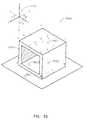
- An object identification systemprovides communication between a monitor and an object, while the monitor and object are within communicating range.
- Each objectincludes a resonant circuit coupled to an antenna used for communication.
- Communicationmay be used to accomplish one or more purposes including: (a) to detect presence of a resonant circuit (e.g., to locate an object as in a zone), (b) to provide operative power to a transceiver, (c) to determine the resonant frequency of such a resonant circuit, (d) to determine a transceiver identification, (e) to receive data from a transceiver, or (f) to send data to one or more transceivers.
- Transmitted power levelsmay vary according to the range suitable for the communication. For example, objects may be detected at a higher transmitted power level and a warning issued that some objects may be out of range for interrogation. Communication may be accomplished using the same or different media or frequencies for different purposes (e.g., magnetic induction, radio, infrared light, or acoustics). Different media or frequencies may be used simultaneously or at different times for the same purpose. When such objects are proximate to each other, the antennas couple the resonant circuits to provide a corporate resonant frequency, typically lower than the resonant frequency of each resonant circuit in isolation.
- media or frequenciese.g., magnetic induction, radio, infrared light, or acoustics
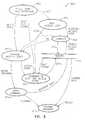
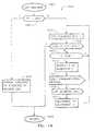
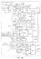
- object identification system 100includes host computer 122, network 128, monitors 124 and 126, antenna systems 120 and 122, sensors 160 and 162, and controls 164 and 166.
- System 100is capable of establishing reliable communication in spite of interference from transmitting sources not part of system 100.
- interference source 190(representative of any number of sources and locations) broadcasts signal 193 (representing one or more frequency components, or noise) within the reception range of antenna systems 120 and 121.
- Host computer 122may include any computer system having computing capacity and interfaces for supporting data communication on network 128 among one or more monitors 124, 126.
- a conventional office computer systemmay be used.
- Host computer 122may operate to receive notice of objects detected or identified by monitors 124, 126 and to conduct any otherwise conventional business process in response to such notice.
- host computermay provide inventory accounting, point of sale services, materials handling, automatic data collection, electronic article surveillance, or electronic access control in response to object detection or identification where objects may include personnel badges, identification tags, transportation tags, inventory labels, electronic keys, authorization devices, or price tags.
- Network 128may include any network for data transfer (e.g., an internet, a wide area network. a local area network using cable, telephony, or wireless technology) between a monitor and a host computer. In addition, network 128 may support data transfer between one or more monitors 124, 126.
- network 128may include any network for data transfer (e.g., an internet, a wide area network. a local area network using cable, telephony, or wireless technology) between a monitor and a host computer.
- network 128may support data transfer between one or more monitors 124, 126.
- Host computer 122may perform a significant proportion of the data analysis, communication (e.g., formation and analysis of messages to and from objects according to one or more protocols for determining identification), and control functions discussed herein with respect to a monitor, when, for example, a monitor 124, 126 is of limited processing capability.
- monitor 124receives commands from host computer 122 and provides reports to host computer 122 via network 128. Commands may include requests by host computer 122 for the current state of controls 164, the current readings from sensors 160, the status of any antenna node 140, 142, and the status of the configuration of monitor 124 or antenna system 120.
- Host computer 122may command monitor 124 to transmit on one or more desired frequencies, may direct monitor 124 to receive on one or more bands (wide or narrow) and/or perform analog and digital analysis of signals received from antenna system 120, and may direct reconfiguration of monitor 124, sensors 160, controls 164, and/or antenna system 120. Further, host computer 122 may, by suitable commands, request notice of objects detected or a list of object identifications currently within communication range of monitor 124, and/or request raw data from which host computer 122 may detect objects or determine such a list. Finally, host computer 122, using suitable commands to monitors 124 and 126, may direct cooperation of monitors 124 and 126 for performing any of the functions discussed above.
- a monitorincludes any system that communicates with one or more objects and provides results of such communication. Results may be provided to an operator at the monitor (e.g., when host computer 122 is omitted) or to a host computer for processing as discussed above.
- System 100may include one or more monitors, several monitors being used for redundancy or when the capacity of a single monitor is exceeded by physical distribution of objects or the desired extent of communication with an expected population of objects in perhaps a limited time.
- monitors 124 and 126may be functionally equivalent and arranged in two geographic zones or territories. When redundant communication with objects by each monitor is not desired, the location of an object as within a particular zone may be ascertained by communication with one of the two monitors 124 or 126. Movement of an object from one zone to another may be determined by host computer 122 from suitable reports by monitors 124 and 126.
- An antenna systemincludes any system for coupling one or more antennas to a monitor for communication between a monitor and one or more objects. When communication from one or more of several monitors is limited to providing operative power, receiving antenna functions of those monitors and antenna systems may be omitted.
- antenna system 120includes antenna bus 132 coupling antenna node 140 and antenna node 142 to monitor 124.
- Antenna node 140supports antennas 150.
- Antenna node 142supports antennas 152.
- antenna system 121includes antenna bus 136 for coupling antenna node 144 and antenna node 146 to monitor 126.
- Antenna node 144supports antennas 154.
- Antenna node 146supports antennas 156.
- an antennarepresents any transducer of energy used in communication including, for example, a lens for infrared light energy or a horn or structure for acoustic energy.
- An alternate antenna systemincludes one or more replaceable modules for reconfiguring operation from any communication medium or frequency band to another medium or frequency band.
- An antenna busincludes any network for conveying signals for coupling one or more transmitters to one or more antennas, for conveying signals for coupling one or more antennas to one or more receivers, and for coupling one or more processors for data communication.
- antenna bus 132couples antennas 150, 152 to transmitters and receivers of monitor 124.
- antenna bus 132couples processors in antenna nodes 140 and 142 with a processor of monitor 124.
- Monitor 124may direct antenna node functions and receive status information by issuing commands to one or more antenna nodes via antenna bus 132.
- more than one monitormay use the same antenna bus.
- monitors 124 and 126may be coupled for communication via antenna bus 132 in place of (or in addition to) communication between monitors via bus 128.
- Communication between a monitor and an objectmay involve one or more antennas.
- communication between monitor 124 and object 103is illustrated with signals 170 from antennas 152 to object 103; and, signal 172 from object 103 to antennas 152. It is not necessary for the same antenna node to operate for sending and receiving communication to a particular object.
- antennas 152provide signal 174 to object 102; and, object 102 provides signal 176 for reception by antennas 150.
- the orientation of an object antennaincludes the orientation of the object antenna with respect to an antenna used by a monitor for communication with objects and includes the orientation of the object antenna with respect to other object antennas.
- coupling of antennas for power transfer from a monitor to an objectmay be primarily by magnetic fields. Such coupling may decrease as the object antenna orientation differs from coplanar (or parallel planes) with respect to the monitor antenna.
- planar object antennasare coplanar (or in parallel planes) with respect to each other, an object may receive power from other objects and the coupling of multiple resonant circuits may effect the behavior of one or more of such resonant circuits.
- a group of objectswhen each object has a resonant circuit with a resonant frequency when operated in isolation, a group of objects may have a peak of energy absorption at a different (e.g., lower) frequency, herein called a stack resonant frequency.
- Some objects in a stackmay not be coupled to the same extent as other (e.g., a majority) objects and so may absorb energy more efficiently at a frequency between the resonant frequency in isolation and the stack resonant frequency of the majority.
- a nonuniform stack of objectsmay exhibit several stack resonant frequencies.
- resonant circuits in such a system of coupled object antennasmay have a detrimental effect on communication.
- Detrimental effectsmay include insufficient operative power being received by a particular transceiver in an object so that other purposes of communication cannot be met; insufficient or discontinuous power to support digital and analog functions (e.g., counting, sensing, converting) so that data communication may be inaccurate; limited range of a signal transmitted by an individual object; and a different than expected power spectral density of a signal transmitted by an individual object.
- Sensors 160, 162measure various aspects of the environment near the respective monitor, while controls 164, 166 effect changes in that environment.
- Sensors 160, 162may include any conventional electronic transducers including, for example, temperature sensors, pressure sensors, proximity sensors, electromagnetic sensors, optical sensors, and mechanical sensors such as used conventionally for detecting environmental physical conditions, movement of objects in a surveillance area, opening and closing of doors, and passage of vehicles, animals, personnel, and/or items not equipped with transceivers.
- sensors 160, 162may include a bar code reader, a video camera, and other conventional product tracking sensors.
- Controls 164, 166may include any conventional facility controls when monitors 124, 126 are stationary; or, may include vehicular controls, as appropriate, for monitors 124, 126 in a mobile configuration. Controls 164, 166 may include controls for changing the orientation of one or more antennas of antenna systems 120, 121. Each monitor 124, 126 integrates and reports information related to events as detected by sensors 160, 162 and related to communication with one or more objects 102 through 112. Such reports may be provided by alarms, speech enunciators, printouts, or displays (not shown). Each monitor 124, 126 may respond to one or more detected events by changing the state of controls 164, 166 and/or reporting one or more events across network 128 to host computer 122 and/or another monitor.
- Sensors and controls as discussed abovemay be supported in an alternate implementation of system 100 from one or more antenna nodes in addition or in place of sensors 160 and 164 supported from monitor 124 directly.
- sensors and controlsWhen supported by an antenna node, sensors and controls may be placed in locations distant from monitor 124 or more suitable for signal routing, system installation, test, or maintenance.
- a node of such an implementationmay support any combination of antennas, sensors, and controls, including configurations of exclusively antennas (as shown), sensors, or controls.
- System 100may be constructed and assembled using conventional electrical and electronic components and techniques including firmware and software developed using conventional software development techniques.
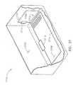
- Objects for use with system 100may be constructed and assembled using conventional electrical, electronic, and mechanical techniques including packaging as integrated circuits, hybrids, smart cards, labels, tags, badges, packing materials, packaging, receptacles, or signage as desired for any of the applications discussed above.
- packagingas integrated circuits, hybrids, smart cards, labels, tags, badges, packing materials, packaging, receptacles, or signage as desired for any of the applications discussed above.
- FIG. 1the functional block diagram of FIG. 1 is not intended to convey other physical aspects of system 100.
- Any of various physical packages and distributions of the functions of system 100may be employed using conventional packaging and data communication technology for desired system operation.
- the functions of host computer, monitor, and antenna systemmay be integrated in one package or partitioned into numerous cooperating or redundant packages.
- System 100may be expanded to include any number of host computers (one shown for simplicity), any number of monitors (two shown for simplicity), and any number of antenna nodes per antenna system (two shown for simplicity).
- Antenna system 120may be integral to a single location, distributed within one or more zones, or mobile.
- objects 102-112may have relatively fixed locations (e.g., embedded in roadways, moving belts, etc.) when monitors are mobile or portable.
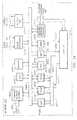
- Objects 104 and 105form stack 114, wherein respective object antennas are coupled to some extent (e.g., more or less aligned in parallel planes or coplanar and/or positioned in more or less close proximity to each other).
- objects 107 through 112form stack 116.
- coupling sufficient to observe a stack resonant frequency different from the resonant frequency of an isolated objectmay occur at distances between parallel aligned object antennas less than 8 inches (e.g., about 1 inch).
- Stack 114 of objects 104 and 105cooperate as described below with reference to FIG. 2.
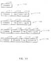
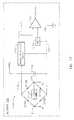
- Each object 104, 105includes an identical transceiver 201, 231.
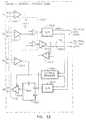
- Transceiver 201includes antenna 202, tank circuit 204, rectifier 206, receiver 208, transmitter 210, and state machine 212.
- Tank circuit 204is a conventional resonant circuit (e.g., a series, parallel, or series/parallel resonant circuit).
- the inductance of antenna 202may cooperate with tank circuit 204 as an additional inductance or as the primary inductance of tank circuit 204.
- Antenna 202when located proximate to antenna 232, may be joined by lines of flux indicated generally as 290. Lines of flux 290 represent magnetic coupling between antennas 202 and 232.
- the effects of magnetic coupling on tank circuit 204include (a) change to the resonant frequency of tank circuit 204, (b) change to the Q of tank circuit 204, (c) loading of transmitter 210 when transmitting, and (d) attenuation of any signal (e.g., power or message) received by receiver 208.
- magnetic couplingmay decrease the energy received for conversion to power by rectifier 206.
- Tank circuits 204 and 234cooperate when coupled (e.g., ring currents in phase, one resonant frequency herein called the stack resonant frequency, and energy sharing) Particular advantages are obtained in system 100 as a consequence of enhancing some of these effects and accounting for these effects in the functions performed by monitor 124 and/or host computer 122.
- tank 204may have a Q in the range 90-130 in isolation, 40-70 when coupled to transceiver circuitry, and as low as 20 when proximate to other transceivers.
- a stack of from 3 to 100 transceivers in coplanar orientationmay have a Q of about 35.
- Each monitor 124, 126may at any suitable time perform a method for selecting one or more frequencies (or bands of frequencies) for communication between the monitor and one or more objects. Upon selecting a frequency (or band) for communication, monitor 124 may proceed further to detect. empower, interrogate or transfer data with one or more transceivers by transmitting and/or receiving messages using the selected frequency (or band).
- method 500 of FIG. 5may be performed by monitor 124, or by the cooperation of host computer 122 and monitor 124 as discussed above.
- a monitormay provide power to transceivers at any time with respect to other communication (e.g., prior to interrogation, interleaved during interrogation, simultaneously on another frequency, or not at all for battery powered transceivers).
- a sequence of frequencies in a desired scan rangeis determined and stored in an array of monitor transmit frequencies for scanning, MTFS [1..A].
- Such a sequence of frequenciesmay include any integer number of frequencies (e.g., as indicated by the variable A) and may be selected from (or stored in) array MTFS in any suitable order.
- a sequence of frequenciesis selected so as to avoid transmitting more than a predetermined average power in any particular band of frequencies.
- a frequency rangemay be divided into any number of bands. Such bands may be of any bandwidth, may overlap, and may omit one or more portions of the range.
- the sequence of frequenciesmay provide for one or more transmissions in a first band followed by one or more transmissions in any other band.
- transmission on a frequency in a first bandmay be followed by transmission of any frequency in a second band (e.g., F324 in band F320 to F328) to limit average power transmitted in the first band.
- a frequency offset from the beginning of a bandmay be used as an offset in another band; although, differing respective offsets in each band may be used.
- any order of frequency transmission described in related patent application S/N 09/088,924, cited abovemay be used.
- Scanningmay be defined for a range about a center frequency divided into an integer number of contiguous bands of identical bandwidth.
- scanningmay be accomplished in a number of subscans.
- Each subscanmay include one transmission in each band at an offset from the lower boundary of the band.
- the subscanmay proceed from band to band in sequential order of increasing frequency.
- the offset used in a first subscanmay be increased by an incremental amount for use in a subscquent subscan.
- N, T, n, s, and tmay all be integers to facilitate computation (e.g., loop counters and limits). Values for s and t may be consecutively selected as integers from the serics of integers indicated by the bounds in the above formulae.
- any seriesmay be used in place of the series of integers, for example, a series of real numbers may be used. Any function may be used to determine a next value of the series, including, for example, a pseudo random number generator.
- any algorithme.g., a look up table, or set of rules
- a suitable offset to be used in each subscan for each bandmay be determined by any suitable algorithm. For example, a pseaudo random number generator may be used to determine a next band and a next offset for a next transmission in that band.
- the amplitute and/or duration of each transmissionmay vary, for example, as a function of frequency, when average power is to be limited into a reactive or resonant load (e.g., a load that is not purely resistive).
- a next frequency that is determined according to a series or algorithm as discussed above,may be omitted from a subscan as a consequence of forecasting the average power that would be transmitted in the band and determinng whether a maximum average power would be exceeded if the transmission were not omitted. Such a determination may include an accounting for prior transmissions over a suitable time period.
- frequencies for scanningmay be chosen in any sequence for determining any combination of operating frequencies of one or more objects.
- scanningmay include frequencies in a range from about 2.5 MHz (e.g., F304) to about 6.0 MHz (e.g., F328) to account for manufacturing tolerances and object orientation (e.g., stacks) as discussed above.
- Array MTFSmay include, for each frequency, values that specify the configuration to be used for transmitting and receiving. Such values may specify configuration parameters for each transmitter (e.g., power level, synchronization, duration, one or more antennas, tuning, and driving phases) and for each receiver (e.g., selection of detector, selection of clocking signals, filter parameters, synchronization, one or more antennas, tuning, squelch timing, and signal processing parameters as discussed below). For efficiency, default values or references to sets of predefined values may be used. Filter parameters and/or signal processing parameters may effect selective attenuation of interference (in time domain or frequency domain) as determined in any prior execution of a step of method 500.
- valuesmay specify configuration parameters for each transmitter (e.g., power level, synchronization, duration, one or more antennas, tuning, and driving phases) and for each receiver (e.g., selection of detector, selection of clocking signals, filter parameters, synchronization, one or more antennas, tuning, squelch timing, and signal processing parameters as discussed below).
- alternate scanning techniquesmay be used including: (a) transmit a narrow band signal and receive with a wide band detector; (b) transmit a wide band signal and receive with a narrow band detector; (c) transmit two or more narrow band signals (consecutively or simultaneously) and receive with a wide band detector; or (d) maintain transmitting of a wide band signal while receiving at consecutive times with different narrow band detector settings.
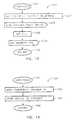
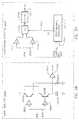
- a scan subroutineis performed in accordance with the contents of array MTFS. Any suitable method of scanning may be used for determining one or more signal properties of candidate frequencies to facilitate selecting one or more frequencies for interrogation. Particular advantages are obtained in system 100 by use of a scan method of FIG. 6. Control may be transferred from step 504 to step 601 of FIG. 6.
- the first monitor transmit frequency for scanningis selected from array MTFS using a loop variable S that is assigned the first index value 1.
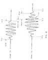
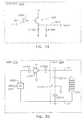
- unmodulated carrier at the frequency indicated by the value MTFS[S]is transmitted from antenna system 120 (e.g., one or more default antennas, or one or more antennas determined in step 502 discussed above) for duration D430 illustrated as signal 170 in FIG. 4.
- Carrier transmissionbegins at time T410 and continues until time T414.
- the rise and fall time of the unmodulated carriermay be substantial as shown in FIG. 4 or (preferably) may be negligible.
- the duration D430is preferably short in comparison to a START signal discussed below.
- Full operation of transceivers 201, 231is not required during scanning. In a preferred scanning method, carrier transmission is insufficient to provide operative power in any transceiver.
- one or more antennasmay be squelched for duration D434 to stop radiation which may interfere with receiving on the same or different antennas.
- the antenna squelch functionis effective on or near a zero crossing of signal 170, as shown at time T414, to avoid transmitting out-of-band noise.
- the squelch operationis complete at time T416.
- the duration D434is preferably less than one period of the frequency being transmitted at step 604 (e.g., from about three periods of the transmitted carrier to less than 1 microsecond, preferably from 1 to 3 ⁇ sec).
- Antennas not in useare squelched or left open to avoid detection of an antenna resonant frequency at step 608.
- Signal 170e.g., a magnetic field
- transceivers 201, 231When received by one or more transceivers 201, 231, will consequently develop an oscillating (i.e., ringing) current in tank circuits 204, 234 and antennas 202, 232.
- Each oscillating currentwill persist after time T414 as a consequence of the Q of the tank circuit.
- a ring signalis transmitted from antenna 202 from time T416 to time T422.
- Signal 172 of FIG. 4illustrates in an approximate fashion the extent of the ring signal.
- signal 172may include the superposition of signals from one or more separate objects and/or one or more stacks, as described above.
- Signal 172is typically several orders or magnitude lower in amplitude than signal 170.
- Signal 172may also differ in frequency and phase from carrier signal 170. These differences in frequency and phase, as well as changes in amplitude of signal 172 between times T416 and T422 convey information about tank circuit 204, about the orientation of transceiver antenna 202 with respect to antenna system 120 and other transceivers, the number of simultaneously ringing tank circuits, and possibly the location and relative movement (e.g. within a zone) of tank circuits with respect to antenna system 120.
- signal 172is received by antenna system 120 (e.g., one or more default antennas, or one or more antennas determined in step 502 discussed above) and sampled for duration D436 between times T416 and T418. Although a shorter duration may be used, the duration T416 to T418 and the sensitivity of the receiver (at signal levels expected to be received in a particular application) are selected to provide about 8 periods of the ring signal for sampling. A number of samples 417 are recorded in monitor received scan array MRS[1..D]. Each sample may indicate an amplitude of signal 172 (e.g., a measured analog voltage converted to a digital representation). In addition, samples may be taken at time T418 through time T422 for further analysis.
- antenna system 120e.g., one or more default antennas, or one or more antennas determined in step 502 discussed above
- duration D436between times T416 and T418.
- duration T416 to T418 and the sensitivity of the receiverare selected to provide about 8 periods of the ring
- various signal propertiesare determined in accordance with the contents of array MRS and similar arrays corresponding to prior performances of step 610.
- Any conventional signal propertymay be determined.
- a particular signal propertymay be determined at a first time (A) and again at a second time (B) (during the expected decay time of a ring signal) and the relationship between signal property magnitudes at A and B may be used to determine a third signal property.
- the analysis of signal propertiesmay proceed in the time domain (e.g., amplitude, phase) or in the frequency domain. Analysis in the frequency domain may proceed from the result of a conventional fast Fourier transform (FFT) of a series of samples (e.g.
- FFTfast Fourier transform
- a sampling window of 5 to 50 ⁇ sectaken beginning at time A (e.g., time T416 for 5 ⁇ sec) and/or beginning at time B (eg., time T418 for 5 ⁇ sec). Examples of suitable signal properties are described in Table 1.
- a signal amplitude at time Ais expected to be greater than a signal amplitude taken at time B. If not, the signal being analyzed may be interference, for example signal 193. The amount of the difference in amplitude should fall within an acceptable range. The range is based on the Q of tank circuit 204 and/or other coupled tank circuits, and the effect of simultaneous ring signals from several coupled or uncoupled transceivers.
- A/BThe ratio of an amplitude taken at time A to an amplitude taken at time B provides an alternate indication of the Q of the ringing tank or tanks, as discussed above. The ratio is expected to fall within a range of Q values for tank circuits and stacks to be encountered by system 100.
- the A/B techniquemay provide more reliable results than the A-B technique at low noise conditions.
- a (at freq 2 )The signal amplitude at each of two or more frequencies (when normalized) provides information that is expected to be consistent with the Q of the ringing tank, or tanks. as discussed above. The difference between the normalized amplitude at any frequency when compared to an expected amplitude (based on a range of Q), if not within or acceptable range may indicate that one or more signal amplitudes correspond to noise or interference.
- Phase at time BThe phase of the signal at time B is expected to correspond to the phase of a decaying sinusoid of phase known at time A.
- the phasemay be determined in any manner including, for example, comparing signals from multiple receivers each having a phase sensitive detector, locking a phase-locked loop at time A for use at time B, or using digital signal analysis.
- the phase at time Bdiffers from the predicted phase by more than a predetermined amount, the signal may be interference.
- FFT(B)Frequency components of the result of an FFT analysis may indicate one or more significant component frequencies.
- the magnitude of frequency components of an FFT taken at time Ashould not differ more than a predetermined amount from the magnitude of corresponding frequency components of an FFT taken at time B.
- FFT(A at freq 2 )An FFT resulting from transmission at a first frequency is expected to have frequency components that correspond to frequency components of an FFT resulting from transmission at a second different frequency.
- the non-different componentmay be a component of an interference signal, for example, signal 193.
- Phase(A at freq 2 )A tuned circuit ring signal is expected to exhibit a strong phase to frequency variation at frequencies near the resonant frequency. If the phase does not vary by more than a predetermined amount as measured at a first and a second frequency, the signal may be interference.
- a a1-a2A(using antenna 1) - A(using antenna 2)
- An amplitude signal(e.g., at time A or B above) may be modified by subtracting the signal as received from more than one antenna. Common mode rejection results.
- the modified signal techniquemay be used in place of any non-modified signals in any of the properties discussed above (e.g., A a1-a2 - B a1-a2 ; A a1-a2 / B a1-a2 ; FFT(A a1-a2 ); etc.)
- a d1-d2A(using wide-band detector 1) vs.
- each signal property determined in step 610is stored in an array at an index position corresponding to the transmitted frequency at step 604.
- several arrays for monitor reply signal propertiesmay be indexed using the loop variable S, as MRSP1[S], MRSP2[S], etc.
- step 614the loop variable S is incremented and a subsequent monitor transmit frequency is selected until all monitor transmit frequencies have been transmitted.
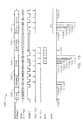
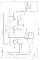
- arrays MRSP1, MRSP2, etc.are analyzed individually and/or by comparison and/or correlation to determine which frequency or frequencies correspond to maximum values of a figure of merit based on one or more signal properties. Correlation may be time coherent or spectral coherent. For example, if a figure of merit is based solely on a single signal property as illustrated in FIG. 3, a conventional array analysis may be used to determine that frequency F324 corresponds to a maximum signal property S384.
- the graph of values shown in FIG. 3may be represented in memory as a list (or array) of frequency-property pairs including, for example, (F304,S360), (F308,S380), and numerous pairs in between.
- Peak values of the signal propertymay be noted in the analysis, including frequencies F308, F312, F316, and F320. Further analysis may determine one or more candidate frequencies in accordance with conventional profile recognition logic and profiles of expected signal properties based on theoretical models, measurements, and analysis. For example, if frequency F324 corresponds to the tank frequency expected for a transceiver operating individually, then frequency F324 would be a candidate. By profile recognition, frequency F320 may be determined to correspond to stack 114 and frequencies F308, F312, and F316 may correspond to stack 116. Using the signal property value S384 for normalization, it may be determined that signal property value S380 corresponding to frequency F308 is also a candidate because its relative amplitude meets or exceeds a threshold value.
- signal amplitude S378 and S374 corresponding respectively to frequency F312 and F316may be of little interest based on the possibility that these minor peaks in signal property value may correspond to object 107 and 112 (or similarly situated objects) having weaker coupling to all other objects 108 through 111 of stack 116 due to being positioned at the respective ends of stack 116.
- frequencies F308, F312, and F316may correspond to a single stack 116 which may be interrogated at a single frequency, for example frequency F308.
- Communicationmay be conducted at frequencies F312 and F316 intentionally for one or more purposes (e.g., transmitting operative power), for example, when it is expected that each frequency respectively corresponds to a different one or more transceivers (e.g., a transceiver detuned for any reason including proximity to another transceiver or to a surface that interfaces with communication as discussed above).
- frequencies F312 and F316intentionally for one or more purposes (e.g., transmitting operative power), for example, when it is expected that each frequency respectively corresponds to a different one or more transceivers (e.g., a transceiver detuned for any reason including proximity to another transceiver or to a surface that interfaces with communication as discussed above).
- further analysismay account for the Q (e.g., quality factor or standard deviation) of the signal property at each peak frequency.
- Qe.g., quality factor or standard deviation
- signal property at frequency F324exhibits a high Q
- signal property at frequency F308exhibits a somewhat lower Q
- signal property at frequency F320exhibits a relatively low Q.
- Some frequencies initially considered candidatesmay be eliminated when the value of the signal property (or figure of merit) does not correspond to a Q greater than a minimum expected Q, or the relative magnitude of the signal property value does not exceed a minimum expected magnitude.
- stack 116which may exhibit a signal property having multiple peak values as illustrated at frequency F308, F312, and F316, further analysis may be employed to determine which of the three possible candidate frequencies is most suitable for interrogation.
- signal propertiesmay indicate the number of objects present, improper orientation of one or more objects, or improper spacing between objects.
- one or more candidate frequenciesmay be subject to further analysis in conjunction with a subscan procedure.
- a suitable range of frequencies proximate to the candidate frequencyis specified for a subscan.
- Any subscan proceduremay be used. Particular advantages are obtained in system 100 by performing the subscan procedure in a manner similar to the scan procedure discussed above with reference to step 504. For example, control may transfer from step 508 to step 701 of FIG. 7.
- Frequency values specified for a subscan in array MTFSmay be accompanied by any of the configuration values (e.g., revised for this subscan) discussed above with reference to Step 502.
- a sequence of frequencies within each desired subscan rangeis determined.
- Values in an array of monitor transmit frequencies for scanningare determined, for example MTFS[1..C].
- a typical subscanmay span a frequency range of ⁇ 200 KHz around a frequency of interest.
- a scan procedureis performed in accordance with the contents of array MTFS. Control may transfer to step 601 and returns from step 616 as described above.
- step 706revised signal property arrays MRSP1, MRSP2, etc. are used to revise one or more figures of merit as discussed above with reference to step 506. Control returns at step 708 to the calling routine, for example, step 510 of FIG. 5.
- each frequency associated with a figure of merit having an appropriate magnitudeis identified in an array of monitor transmit frequencies for interrogation. For example, MTFI[1..B].
- each interrogation frequencyis used in the conduct of an interrogation scenario.
- Any interrogation protocol and modulation methodmay be used. Suitable interrogation protocols are described in TABLE 2.
- An interrogation protocol for use in system 100includes any conventional protocol for the transfer of an individual identification from a transceiver to a monitor, as well as any protocol from which a monitor may determine an individual identification. Subsequent communication employing the individual identification may then proceed without collision, interference, or ambiguity in system operation.
- Any message format and modulation methodmay be used, preferably a narrow-band modulation, for example, any pulse width modulation (PWM) technique.
- PWMpulse width modulation
- Transceiver identificationmay include the frequency (or frequency band) in which communication can be reliably established, a code or sequence of codes recognized by the transceiver for enabling one or more replies, a code indicated in (or by) a reply, or a combination of these features.
- Protocol Description 1Time for beginning transmission of reply message may be determined by the object's transceiver according to a random number to decrease probability of collision. Long reply messages may be used.
- Object or monitor (or both)may include a mechanism for collision detection to initiate retry. Content of reply message may convey identification. 2 All objects may have an assigned reply slot number. Object identification may be communicated in N parts in the corresponding reply slot in reply to N requests. Content of reply slot may convey identification.
- Objectsmay reply redundantly in more than one reply slot in reply to a single request. Collision detection may be used by the monitor to determine whether data in a particular reply slot is valid. Content of one clear reply slot may convey identification. 4 A particular address or a group address may be sent with the interrogation message. Objects may reply when addressed in particular or as members of the requested group. Failure to be addressed may impose an initial state (e.g., reset), preventing further replies. Context of a particular address may be implied from immediately preceding group address(es). When addressed, a reply in a particular reply slot may indicate a next address in a predetermined sequence. Being addressed may silence replies after a predetermined minimum number of replies (e.g., one).
- Content of reply slotmay serve for reliable detection or for additional identification.
- a relatively long identification numbermay be broken up into several shorter access codes, each access code associated with a level.
- Objectsmay be addressed in any sequence of access codes. When sufficient access codes have been received, a reply in a particular reply slot may indicate an access code for another level in a predetermined sequence, a final portion of the identification number, or data provided to the monitor. Groups of objects may be programmed with identical access codes at predetermined levels for obtaining replies in a particular reply slot indicating an access code at a predetermined level.
- Content of reply slotmay be for reliable detection, additional identification, or providing data to the monitor. 6
- Presence of individual and coupled groups of object transceiversmay be determined. Identification may be determined in part by a frequency of a response signal.
- a group of transceiversmay be enabled (turned on) in accordance with one frequency of response.
- Each reply time slotmay be assigned or directed to be self-assigned (e.g., randomly). Reception of replies may be restricted to a narrow band (e.g., notch) to ignore objects not in the desired group.
- Time slotsmay be read in one or more messages addressed to subgroups. Identification may be determined from slot number of reply and/or content of reply. A subgroup may be turned off or automatically disabled. Interrogation may continue for another subgroup or frequency until all portions of identification have been determined. 7 Any combination of techniques illustrated by the above protocols may be used in full or in part.
- Controlmay transfer from step 512 to step 1201 with reference to FIG. 12.
- the selected frequencies at step 510may be used for interrogation, or, alternately, these frequencies may be used for transferring power from monitor 124 to one or more objects 102 through 112.
- interrogationmay proceed in any conventional manner on any suitable frequency.
- an object of the present invention having a tank circuit that cooperates with the tank circuit of proximate transceiversmay receive energy from a broadcast at a frequency that is near the resonant frequency of the tank circuit. Further, such a transceiver may respond and participate in an interrogation scenario at another frequency (eg, 250MHz to 350 MHz) using conventional RFID.
- the interrogation protocol and transmission modulation techniques used in conventional RFIDinclude, for example, frequencies selected for suitable propagation characteristics, infrared and other optical frequencies, and ultrasonic and other audio frequencies.
- Magnetic coupling between proximate transceivers as described above with reference to FIG. 2may be obtained at any frequency suitable for the dimensions of antennas and distances between antennas for the desired communication purpose. Magnetic coupling is preferred for providing a power signal so as to limit the range of the power signal to meet regulatory guidelines.
- Modulation techniquesinclude, for example, spread spectrum, amplitude modulation, frequency modulation, single side band modulation, and off/on keying (OOK) modulation.
- OOKis preferred for its narrow frequency spectrum, permitting communication in the presence and orientation of other objects that absorb portions of wider-band modulation to an unpredictable extent.
- the complexity of circuits and firmware for performing the functions of a transceivermay be reduced by employing one or more of the following techniques in combination: (a) receiving operative power for the transceiver via the antenna and tank as described above; (b) employing transceiver detection (e.g., detecting a ring signal) at the same frequency that is used to power the transceiver; (c) employing OOK modulation for interrogation; (d) conducting interrogation at the same frequency as used for powering the transceiver; (e) limiting the reply from a transceiver during interrogation (e.g., one or two bits); (f) employing multiple predetermined reply slots for multiple transceivers to reply to a single command; (g) using predetermined durations of unmodulated carrier for one or more transceiver reset operations; (h) employing a transceiver identification number of sufficient resolution to practically reduce the possibility of collision in an expected operating environment to a negligible amount (e.
- transceiver detection
- monitor 124 and transceiver 201will be described below in an implementation that includes all of the techniques listed above.
- firmwaree.g., state machine microcode
- softwaree.g., microprocessor instruction code
- an exemplary implementationsupports interrogation and further supports read/write data communication.
- the process 800 of FIG. 8may be performed by a transceiver 201, in order to support such a protocol.
- Process 800includes processes for the detection of START and SEPARATOR signals 802; awaiting an access code 804; changing an access state 810; comparing an access code to an access code from memory 806; transmitting a reply in a reply slot in accordance with an access state 812: awaiting a command 814; and transmitting a message 816.
- Processesmay be supported in any combination of software, firmware, or logic circuits. Execution of these processes may proceed in an interrupt driven, polled, single threaded, or multitasking parallel execution manner. As discussed below, a process notifies another process in any conventional manner, for example using a common variable, giving a command, producing a signal, etc.
- Process 802continuously analyzes received carrier for indications of a START signal and a SEPARATOR signal. Uninterrupted, unmodulated carrier for more than a first predetermined duration may indicate a START signal. When a START signal is received, process 804 may be notified. When a START signal is detected, the state of the transceiver should be reset to a known initial condition. Process 802 provides such notice to process 810 to reset the access state. Uninterrupted, unmodulated carrier for a second predetermined duration (preferably less than the first predetermined duration), may be used to indicate a SEPARATOR signal. A SEPARATOR signal, as used herein, may indicate an interruption in a message and thereby indicate the onset of a subsequent message.
- process 802Upon detection of a SEPARATOR signal, process 802 provides notice to process 812 to terminate any transmission which may be in progress or scheduled to be transmitted. Process 802 to process 812 provides notice to reset the slot count accordingly. Failure to receive a proper START signal may leave transceiver 201 in a power-off, reset, condition. Failure to receive a proper SEPARATOR signal may leave the transceiver expecting the completion of the current message format.
- Process 804examines incoming demodulated carrier beginning from a notice of a START signal until a predetermined time when an access code is expected according to the message format.
- a protocol supported by process 800divides the individual transceiver identification into one or more access codes. Each access code is associated with a so-called level code to be discussed below.
- Process 804passes the received level code and access code to process 806 on receipt.
- Process 806operates on a valid received level code and access code when provided by process 804.
- Process 806uses the level code as an address or index into an array stored in memory 808 to retrieve a stored access code. Further, process 806 compares the stored access code with the received access code and provides results of that comparison to process 810 in various protocols supported by process 800. Note that it may not be necessary for access codes to be received in any particular sequence in as much as each access code is received with an associated level code facilitating an appropriate access code to be retrieved from memory in accordance with the level code. Alternatively, any suitable sequence may dictate a desired access state change, as discussed below.
- Process 810changes the access state of transceiver 201.
- process 810resets all access state bits.
- process 810may set one or more access state bits.
- process 810sets an access state bit in accordance with the level provided by process 804 when a suitable result of comparison indicates that the received access code exactly matched the stored access code.
- Process 810provides the current access state to process 812 and, upon obtaining a predetermined access state, may command process 814 to begin a command/reply session.
- Process 812is enabled to transmit when the access state provided by process 810 meets or exceeds a predetermined enabling access state (i.e., the transceiver has been addressed to any extent defined by the protocol).
- Process 812retrieves a slot count from memory 808 in accordance with the level code provided by process 804.
- slotsdesignated with predetermined counts
- Transmit process 812after lapse of the predetermined delay, counts predetermined slot time durations (or slot boundary signals) until the slot count is achieved.
- Process 812then transmits a reply signal in the slot corresponding to the slot count retrieved from memory.
- process 812By transmitting a reply signal in a predetermined reply slot, process 812 as executed in multiple identical transceivers, provides a reply that, on receipt by monitor 124, indicates that one or more transceivers have been enabled to transmit as a consequence of having received one or more suitable access codes.
- Each access codemay represent a group (or subgroup) identification number.
- the individual transceiver identificationmay consist of a (GID) number, a subgroup identification number (SGID), a sub-subgroup identification number (S 2 GID), etc. to any number of levels.
- GIDgroup identification number
- S 2 GIDsub-subgroup identification number
- an individual transceiver identification numberconsists of a 40-bit binary number. This identification number is sufficient to identify uniquely more than one billion transceivers in each of more than 1,000 independent operating environments.
- Each operating environmentis identified by a 10-bit group identification number (e.g., a top level access code) with 30 bits remaining for identification of individual transceivers.
- Process 814upon notice of a begin session command, from process 810, performs any suitable command/reply protocol which may differ in structure and function from the interrogation protocol described above with reference to processes 802 through 812.
- the command/reply protocolmay include commands to send data to a transceiver and to obtain reply data from a transceiver beyond the 1 bit transmit capability discussed above with reference to process 812.
- Process 814may store received data in memory 808 and provide a command to process 816.
- Process 814may continue for multiple command/reply exchanges until: (a) operative power is no longer provided (or commanded to be removed) by monitor 124; (b) a command addresses and changes one or more enabling access state bits in one or more transceivers; or (c) the completion of a command by a transceiver is accompanied by an automatic change of one or more enabling access state bits.
- Process 816receives a command from process 814 and may recall data stored in memory 808 and/or obtain measurement data from a conventional sensor (not shown). Data from memory and/or one or more sensors may be transmitted by process 816 in any suitable manner in accordance with the protocol discussed above with reference to interrogation, the protocol discussed above with respect to a command/reply session, or any conventional protocol.
- a protocol supported by process 800may include a variety of commands as discussed below with reference to FIG. 9.
- commands 904 and 912may represent a minimum configuration.
- Commands 902, 904, and 906affect the access state of a transceiver.
- Command 902resets an access state bit.
- Command 902may be omitted in a simplified variation, where resetting all access state bits is accomplished by ceasing to supply operative power to a transceiver. Because power is supplied from monitor 124 by broadcasting carrier, the need remains in some implementations of system 100 to reset one or more particular access state bits in a group of transceivers or in one transceiver without affecting the access state of unaddressed transceivers.
- Command 902 in combination with one or more access codeswill provide the facility for resetting one or more access state bits as defined in a conventional manner by suitable additional codes accompanying (or integral with) the command.
- Command 904is used to set an access state bit in one or a group of transceivers. As discussed above, command 904 may be used to accumulate a sufficient number of prerequisite set access state bits in order to enable process 812. In a variation of the interrogation protocol discussed above, command 904 may be used to set any arbitrary pattern of access state bits, perhaps in a predetermined sequence, to facilitate any purpose of communication as discussed herein.
- Command 906is used to clear the slot counter in all transceivers. By clearing the slot counter, this command assures that no further replies will be attempted by transceivers without the occurrence of a subsequent command, possibly including further access codes sufficient to obtain the access state required for operation of process 812. Command 906 may be omitted in a system implementation wherein no message is terminated before such message is allowed to proceed to completion. In a system using command 906, efficiencies may be obtained by clearing the slot counters when all expected (or significant) replies have been received.
- Commands 908 and 910accomplish sending data to transceivers from monitor 124.
- Command 908may be used to transfer data from monitor 124 for storage in memory 808 in one or an addressed group of transceivers.
- Command 908may require a prerequisite access state for group identification, security, or reliability purposes.
- Command 910may be used to configure one or more sensor configuration registers so as to control any conventional aspect of sensor operation (e.g., the time a measurement is begun, the duration during which a measurement is taken, the resolution or accuracy of the measurement, designation of any measurement analysis, etc.).
- Commands 912 through 920may be used to obtain data from a transceiver.
- Command 912may be used in the interrogation protocol as discussed above to indicate the existence of an addressed transceiver.
- a transceivermay reply with a 1-bit acknowledgement in a reply slot corresponding to that transceiver's respective membership. For example, if a group of transceivers is addressed, each transceiver may reply with an acknowledgement in a respective reply slot corresponding to that transceiver's membership in a particular subgroup of that group.
- the transceiver receiving command 912may reply with an acknowledgement in a respective reply slot corresponding to its identification number (e.g., the least significant portion of the identification number, i.e., a member identification number).
- command 912may be combined with command 904 to the effect that when a reply is made to command 912 an access state bit is also set.
- Particular advantagesare obtained in system 100 by providing command 912 in a form with the setting of an access state bit (as in command 904) and in another form wherein no access state bit is affected.
- Commands 914 and 916may require that the command be directed to a transceiver that has been fully addressed so as to assure that only one transceiver will attempt to respond to the command. For example, assuming data from memory and sensor data exceeds one bit in length, one transceiver can reply with data from its memory in response to command 914 (or one transceiver can reply with sensor data in response to command 916) without collision, only when monitor 124 has identified one transceiver to send the data and has fully addressed only that transceiver. The length of data to be supplied in one or more replies to commands 914 and 916 may vary.
- Commands 918 and 920demand a reply from one or a group of transceivers.
- the reply to command 918may consist of one dibit, two redundant bits, or a short sequence of bits (e.g., preferably one bit) in each reply slot corresponding to data from memory.
- 1,000 transceiversmay respond with one bit each until all bits of data from memory have been provided.
- the reply to command 920may provide data from up to 1,000 sensors with one bit per sensor in each reply slot.
- commands 918 and 920are directed to a fully addressed transceiver. Such a transceiver provides a reply from which a 10-bit memory value or sensor value may be determined.
- a 1-bit replyBy replying in a reply slot corresponding to the appropriate value (e.g., 1 to 1,000), a 1-bit reply specifies a decimal number to one part in 1,000. When 1024 reply slots are used, a 1-bit reply conveys a 10-bit binary value.
- a command/reply sessionmay be used to accomplish one or more of the functions described in Table 3.
- Purpose Command/Reply Session Tracking An identification of the monitormay be written into transceiver memory by a suitable command and may include monitor location (if not implicit), monitor operator identification (if any), and time-date or process codes (e.g., materials handling or manufacturing step). Replies may indicate time-date when last addressed, monitor identification when last addressed, or listed history of time-date and monitor identifications when addressed.
- Repliesmay be restricted in scope to one or more commands of interest (history of changes to sensor configuration, changes to identification, etc.).
- Security One or more access codes(at one or more levels) may be revised with a suitable command sequence including confirmation of the new code (e.g., repeat what was commanded or send partial or complete identification) prior to enabling use of the new code, and directing use of the new code.
- a programmed set of alternate access codesmay be enabled. These techniques may be used to implement code hopping. Any of the identification features discussed above may be confirmed, rewritten, or subject to selection among predetermined alternatives by one or more suitable commands to accomplish re-identification of one or more transceivers. For example, transceiver VCO center frequencies may be reassigned and/or tank properties may be modified (e.g. by introduction of switched elements, digital control, or other tuning techniques).
- command formats 1004 through 1007 of FIG. 10may be sufficient to provide interrogation and identification of up to 1 billion transceivers in 1,000 applications as discussed above.
- Particular advantages obtained in system 100 according to various aspects of the present inventionby expanding the set of commands to include commands 1000 through 1003 of FIG. 10.
- the expanded set of commandsmay be used during interrogation, assembly, or test to determine, for example, a 40-bit transceiver identification number without proceeding through a hierarchical interrogation sequence.
- each command 1000 through 1003provides an argument identifying a group identification number. No prerequisite access state bits must be set.
- the reply from each transceiveris similar to the reply described with reference to command 912, except that transceivers will respond with a sub-group identification number to command 1000; will respond with a sub-sub-group identification number to command 1001; will respond with a sub-sub-sub-group identification number in reply to command 1002; and will respond with a sub-sub-sub-sub-group identification number in reply to command 1003.
- Commands 1000 through 1003may be used to (a) determine or confirm the complete identification of a physically isolated transceiver; (b) determine or confirm all or part of an identification number of one transceiver when all other transceivers have been disabled; (c) quickly estimate the number of transceivers within communication range; (d) quickly detect the possibility that transceivers may have moved into or out of communication range; or (e) confirm that a particular subgroup of transceivers is not within communication range.
- commands 1004 through 1007each set an appropriate access state bit.
- commands 1005 through 1007may reset the transceiver access state logic if the prerequisite state bit is not already set.
- command 1004is first provided with a level 1 group identification number in order to obtain information as to level 2 sub-group memberships of all addressed transceivers.
- the reply slotsindicate the level 2 sub-group identification number of those transceivers addressed by the group identification number.
- state bit B0 of access state logicis set.
- the level 1 group identification numberis preferably a 10-bit access code.
- the level 2 sub-group identification identified by a reply slotindicates a 10-bit access code.
- command 1005provides the level 2 sub-group identification number as its argument, and elicits the level 3 sub-sub-group identification number from addressed transceivers that are members of the group identification and sub-group identification as indicated by prerequisite state bit B0 and successful comparison of the provided sub-group identification number and the level 2 access code retrieved from memory.
- transceivers that are members of the group and sub-groupwill set state bit B1 corresponding to level 2.
- command 1006is provided with level 3 sub-sub-group identification number as an argument. Transceivers having successfully passed commands 1004 and 1005 will have set the prerequisite state bits B0 and B1.
- a reply to command 1006provides the level 4 sub-sub-sub-group identification number indicated by the corresponding numbered reply slot.
- access state bit B2is set corresponding to level 3.
- command 1007provides the level 4 sub-sub-sub-group identification number as the argument and elicits in the respective reply slot the member identification number of those transceivers that have successfully passed comparison of the group identification number, sub-group identification number, and sub-sub-group identification number as indicated by prerequisite state bits B0, B1, and B2 being set, and, further, successful comparison of the sub-sub-sub-group identification number provided with command 1007 and the level 4 access code retrieved from memory. That transceiver that has successfully replied to command 1007 will also set access state bit B3.
- a system manager of a system 100may arrange transceiver identification numbers so as to assure that the identification number provided by commands 1004 through 1007 will always address exactly one transceiver.
- command 1008may be used with an appropriate argument to read or write data into memory or a configuration registration of a sensor or read data from a sensor or from memory as discussed above.
- a reply to command 1008(e.g., in a particular reply slot) may provide a write acknowledgment or provide a 10-bit data value from a sensor or memory location as discussed above with reference to command 918 and 920. Further setting of access state bits may be unnecessary for command 1008. In a variation, further access state bits may be defined and set by various commands of the type described above with reference to command 1008 to accomplish more sophisticated transceiver functions.
- the commands and arguments discussed with reference to FIG. 10may be arranged in message formats in any conventional manner. Particular advantages are obtained in system 100 according to various aspects of the present invention, using the message formats of FIG. 11.
- message format 1100consisting of a binary code identifying a command 1101 may be used to accomplish commands 902 and 904. These commands require no argument when the command identifying code implicitly identifies one or more access state bits.
- Message format 1110may be used for commands 914 and 916.
- Message format 1110includes command identifying code 1111, pad 1113, and reply bits 1114.
- Pad 1113when used, conveniently separates command code 1111 from reply bits 1114 and assures reliable recognition in the transceiver of the first reply bit of reply bits 1114.
- Reply bits 1114may include any number of bits in serial format.
- Message format 1120may be used for commands 912, 918, and 920 discussed above.
- Message format 1120includes command code 1121, pad 1123, and reply slots 1125.
- Reply slots 1125identify numbered periods of time. Each slot being used for a reply.
- a replymay consist of one or more bits. however, 1-bit reply slots are preferred. In an alternate reply slot configuration, a 1-bit reply may be presented as a dibit consisting of the reply bit in both true and compliment form.
- Message format 1130includes command code 1131, argument 1132, pad 1133, and reply slots 1135.
- Argument 1132may be any binary code.
- argument 1132may convey a level code and an access code as discussed above.
- Message format 1140may include command code 1141, argument 1142, pad 1143, and separator 1146.
- Separator 1146may include uninterrupted, unmodulated carrier as discussed above.
- pad 1143may include a period of time during which no carrier is transmitted.
- command codes 1101, 1111, 1121, 1131, and 1141are of identical structure.
- pads 1113, 1123, 1133, and 1143are of identical structure and may provide delay for processing a received command and argument.
- Reply slots 1125, and 1135are of identical structure and function.
- Arguments 1132, and 1142may be of identical structure or may vary as desired and indicated by corresponding command codes.
- step 512An example of a method to conduct an interrogation at monitor transmit frequencies of interrogation according to step 512 is presented below within the context of process 800 executing in each transceiver. Control may transfer from step 512 to step 1201 of FIG. 12 for performance of the interrogation method of FIGs. 12 through 14.
- variable Cis set to 0 to indicate a command of the form 1000 of FIG. 10. is to be issued.
- Variable RSis set to 1 to indicate a first reply stack is to be used to store replies.
- Variable Gis set to a group identification number of interest. Variable G may be a suitable structure for numerous values as discussed below. When a group identification number is used to distinguish one of 1000 installations of system 100, the group identification number may correspond to a customer number, a geographic area, a political territory, and/or any arbitrary indication that uniquely specifies this installation for the purpose of eliminating confusion with transceiver identification numbers that are properly members of a different system installation. Commands 1000 through 1007 are identified by values 0 through 7 of variable C, respectively.
- step 1204a subroutine is called to send the command and store the replies on an appropriate stack. Control transfers to step 1301 of FIG. 13.
- a message in format 1130is broadcast from monitor 124 with command code 1131 set to the value of the variable C (initially 0) and argument 1132 set to the value of the variable G (initially the group of interest).
- a value indicating a reply was detectedmay be stored on a stack identified from an array of stacks indexed by the variable RS.
- interrogationproceeds according to a tree search algorithm wherein at each node up to 1000 replies are cataloged. Each stack therefore corresponds to one of the nodes traversed in a modified depth-first tree search.
- information associated with each replymay also be stored on the appropriate stack.
- Such informationmay include: (a) the reply slot number; (b) signal amplitude samples 417; (c) frequency domain results of one or more fast Fourier transforms of samples 417; (d) one or more signal properties; and (e) a figure of merit as discussed above with reference to FIGS. 3 and 4. For efficiency, pointers to such information may be stacked instead.
- controlreturns from the send/stack subroutine back to step 1206 of FIG. 12.
- variable Cis set to 3 as an initial condition for the subroutine called in step 1208.
- a subroutineis called to list member identification numbers.
- This subroutineis a recursive subroutine which accomplishes the modified depth-first tree search as discussed above beginning from the current value of variable RS initially set to 1. Control transfers from step 1208 to step 1401 of FIG. 14.
- variable RSindicates a level code as described with reference to FIG. 8.
- Command 1004having already been accomplished at step 1204, RS will proceed from the value 1 to a maximum value of 4 corresponding to commands 1004 through 1007 discussed with reference to FIG. 10. Having received control from step 1208, the test at step 1402 will fail and control will pass to step 1406.
- variable Gis assigned the value (or values) popped from the top of STACK [RS].
- the access code to be used for the value Gis obtained from a table look-up operation (e.g., code conversion mapping). For example, the number of a reply slot is used as an index into an array and the value from the array is assigned to G for use as an access code.
- a level codemay be used as part of the index and the array value may identify a suitable level code in addition to the access code.
- step 1408it is determined whether process 1208 has proceeding to the end of STACK [RS]. If so control passes to step 1402 for a return from this particular call of the list members recursive subroutine. If not, control passes to step 1410.
- step 1410the validity of the value (or values) of variable G is determined.
- This validity testmay proceed in a manner similar to determining whether a particular reply represents a candidate frequency as described at step 506 and 510 above.
- This analysismay include analysis of time domain results, frequency domain results, signal properties, and figures of merit. provided that sufficient information has been stored on STACK [RS].
- Time domain analysismay compare the signal received or properties (e.g., rise time, decay time, envelope shape, or relative time of peak amplitude) with expected values or properties in accordance with the Q of tank 204 and power limiting characteristics discussed below with reference to signal REPLY of FIG. 16. If it is determined that variable G does not represent a valid transceiver, control passes back to step 1406 for obtaining another value from STACK [RS]. Otherwise, control passes from step 1410 to step 1412.
- variables C and RSare each incremented. By incrementing the value of variable RS, results will be stored on a new (empty) stack. By incrementing the value of variable C, preparations are made to transmit a command at the next level.
- send command and stack replies subroutine 1204is called from the context of the current level and current command set at step 1412.
- message format 1120or preferably 1130 may be used.
- message format 1130alone or preferably prefixed by any suitable number of message formats 1140 may be used.
- Prefix message formats 1140when used, assure proper access state bit prerequisites are met by contents of respective arguments 1142. Prerequisites may have been reset by loss of operative power or by reset as discussed below.
- step 1416a recursive call is made to the list members subroutine within the context of the current value of variable RS. Control transfers to step 1401 and upon completion returns from step 1420.
- variables C and RSare decremented to restore the context of the current execution of recursive subroutine list members 1208. Processing in the loop consisting of steps 1406 through 1417 continues until all replies have been considered from STACK [RS]. When all replies have been considered, control passes from step 1408 to step 1420 and a return to a prior call of list members subroutine 1208 is effected. During execution of list members subroutine 1208 at the deepest level (i.e., the highest value of variable RS), control is transferred from step 1402 to step 1418.
- step 1418the respective reply slot numbers of the replies received in response to the command sent at step 1302 are appended to an array herein called the member list.
- the member listAs a result of the tree search algorithm, values from STACK [RS] are appended from time to time until the list members subroutine has reached the end of the stack at the initial level of the tree (i.e., level equals 1 and RS equals 1).
- the return from step 1420passes control to step 1210 of FIG. 12.
- interrogate subroutine 512 of FIG. 12returns control to method 500 at step 512. Processing continues at step 512 to select another monitor transmit frequency for interrogation from array MTFI as indexed by loop variable N until loop variable N exceeds the value B. For each frequency, interrogate subroutine 512 beginning at step 1201 is called for an appropriate tree search. At step 1418, redundant identification numbers may be appended to the member list. Consequently, step 1418 may include a test to forego appending a transceiver identification number to the member list unless it is not already on the member list. Upon completion of interrogation at each monitor transmit frequency for interrogation, control transfers to step 514.
- the contents of the member list arraymay be reported to host computer 122.
- This reporting functionmay be accomplished (or accompanied) by a printout, display, alarm, etc., at monitor 124 as discussed above. Further, the function of reporting identified transceiver identification numbers may be accomplished by suitable file storage or conventional communication between programs operative on host computer 122 and/or monitors 124, 126.
- host computer 122 and/or monitor 124may initiate any command sequence including, for example, command 1008 for commands 914 through 920 as discussed above. Following completion of all individual command/reply sessions (if any), control passes to step 518 where method 500 may repeat beginning at step 502 for continuous monitoring.
- interrogationmay proceed immediately upon detection of a response believed to be transmitted by a transceiver. Further, a command/reply session may be performed immediately upon determining a transceiver.
- the internal iteration loops in each of steps 502 through 516 in such an alternate methodare replaced with appropriate controls on the major iteration loop of step 518.
- steps 502 through 508may be omitted when no additional transceivers are expected to have recently entered communication range.
- Selected interrogation frequencies of array MTFImay be omitted when use provided no identification not already known by use of other interrogation frequencies.
- Step 512may then be performed with a minimum of redundancy to decrease time spent interrogating.
- steps 510 through 514may be omitted and step 516 executed repeatedly for a list of specific transceiver identifications.
- step 512may be repeated with specific (non-redundant) frequencies to receive acknowledgement from each transceiver by fully addressing the transceiver via its known complete identification.
- Monitoring presence of a known populationgenerally is accomplished in less time than interrogation of an unknown population.
- the time spent performing an interrogationmay be reduced by addressing and communicating with members of such known groups (or subgroups to any level).
- interrogationmay be fashioned to ignore replies or avoid facilitating replies from transceivers of such a group (or sub-group).
- Step 512may be omitted for object identification systems where mere presence of one or more objects is all that is desired to be monitored, for example, setting an alarm on detection of any object carried through a passage. Monitoring of objects in the presence of other objects may be accomplished in an alternative implementation. For example, an alarm may be set on detection of any object through a passage, except when accompanied by detection of another predetermined object (e.g., a transceiver in a badge of an authorized person).
- another predetermined objecte.g., a transceiver in a badge of an authorized person.
- Step 508may be omitted when step 506 provides sufficient resolution of one or more frequencies.
- a method for improving reception of a reply signal during interrogation or data communicationincludes the steps of: (a) transmitting a carrier signal at a first frequency; (b) sampling a reply signal, (c) identifying one or more frequency components not expected to be part of a proper reply signal; and (d) programming a filter to attenuate such frequency component(s).
- the transmitted carriermay be at a tank resonant frequency, a stack resonant frequency, or a frequency suitable for use with a tank circuit loosely coupled to a stack. Sampling and identifying frequency components may be accomplished in any manner including further time domain signal processing and/or frequency domain signal processing, as discussed above.
- the filtermay include a digital filter, programmable element network, or a programmable active filter.
- the filter characteristicmay include a low-pass, band-pass, notch, comb, or hi-pass transfer function. Transmitting and sampling may occur during a reply slot.
- a method for improving the accuracy of an interrogation scenarioincludes the steps of: (a) determining a first series of amplitude samples of a reply signal; (b) comparing the first series to a second series of amplitude values expected for a resonant circuit response; and (c) proceeding in the protocol of the interrogation scenario in accordance with whether the extent of comparison exceeded a threshold value.
- a transceiverincludes any circuit for performing the process discussed above with reference to FIG. 8.
- a transceiver 201 capable of performing the command set of FIG. 10 using the message formats of FIG. 11may receive and send data using a combination of off-on keying (OOK) and duty cycle modulation.
- OOKoff-on keying
- rectifier 206may be better understood from a timing description of signals used in transceiver 201.
- An interrogation scenarioseveral messages may be received by a transceiver. Each message to which a reply is expected from any transceiver constitutes a query.
- An interrogation scenariomay include several queries.
- FIG. 15presents signal TANK as it would appear across lines 217 and 219 (i.e., the difference of signals N1 and N2). Portions of signal TANK correspond to portions of an interrogation format 1500 which includes start portion 1593, preamble portion 1594, message type portion 1595, message portion 1596, and reply slots portion 1597.
- Signal TANKis rectified by rectifier 206 to provide DC voltage V+ which is used to power all circuitry of transceiver 201.
- Signal TANKis demodulated by receiver 208 to provide signal DEMOD on line 214.
- signal TANKincludes by superposition the output of transmitter 210 in response to modulation signal MOD on line 216.
- transceiver 201receives unmodulated carrier on signal TANK.
- the period of time from time T1502 to time T1504represents a START signal 1593 as discussed above with reference to process 802.
- the duration of the START signalshould be sufficient to energize rectifier circuit 206 for the provision of continuous power to transceiver 201 for the duration of operation required by the interrogation protocol.
- signal TANKexhibits a series of periods of 50% duty cycle modulation sufficient for establishing proper timing signals for use within transceiver circuitry 201.
- signal CELL CLKis derived from signal DEMOD on line 214 and signal RX CLK is derived to have active edges in the midpoint between the active edges of signal CELL CLK.
- Signal CELL CLKrepresents a cell clock which marks by its active edges the trailing edge of each cell used for communication of one data bit. From time T1504 to time T1506 no carrier is being received. From time T1506 to time T1510 carrier is being received. This pattern of off/on keying is repeated for the entire preamble portion 1594 until time T1516. The length of preamble portion 1594 should be sufficient for generating all timing signals for use in transceiver circuitry 201.
- Received clock signal RX CLKhas an active edge in the middle of each data communication cell for discriminating between cells conveying a logic "0" and cells containing a logic "1".
- Cell content clocked by signal RX CLKis illustrated as signal RXD conveying a "010" pattern for message type portion 1595.
- the logic "0" of signal RXDis derived from a cell containing modulation in only the latter portion of the cell duration. For example, no carrier is received from time T1516 to time T1520; however, carrier is received from time T1520 to time T1522.
- the duration from time T1520 to time T1522 divided by the cell durationrepresents a duty cycle of from 10% to 45%, preferably 40%.
- the active edge of signal RX CLKoccurs while signal DEMOD is low at time T1518 from which signal RXD is determined as a logic "0".
- next cell beginning at time T1522 and extending to time T1530includes a portion from time T1522 to time T1524 where no carrier is being received and a portion from time T1524 to time T1530 during which carrier is being received.
- the duration from time T1524 to time T1530 divided by the cell duration (from time T1522 to time T1530)represents a duty cycle (different from the duty cycle of the cell from T1516 to T1522) of from 55% to 90%, preferably 60%.
- the active edge of signal RX CLKoccurs while signal DEMOND is high at time T1526 from which signal RXD is determined as a logic "1".
- the following cellextends to time T1534 and exhibits another logic "0".
- Message type portion 1595 of interrogation format 1500extends from time T1516 to time T1534. Following message type portion 1595, message portion 1596 extends from time T1534 to time T1550.
- signal TANK and signal DEMODconvey data using off/on keyed modulation, preferably with 40% and 60% duty cycle modulation.
- each bit of message type portion 1595is sent as two complementary bits in sequence (e.g., a dibit) to facilitate a form of redundancy for message validity testing.
- command and/or argument portions of any message format 1100, 1110, 1120, 1130, or 1140may be sent as dibits.
- Reply slots 1597include a reply slot for each reply.
- the duration of a reply slotis equivalent to one period of signal CELL CLK. For example, from time T1550 to time T1554 no carrier is received; however, from time T1554 to time T1558 carrier is received.
- the signal received from time T1554 to time T1558serves several functions including: to maintain power supplied by rectifier circuit, to mark a boundary between adjacent reply slots, to define a duration (e.g., a cell clock period) for synchronizing other clock signals (e.g., a signal 8 times the cell clock frequency), to identify the beginning of an offset into the reply slot for signal detection (e.g., placement of the active edge of signal RCV CLK), and to identify the beginning of an offset into the reply slot for transmitting a reply signal.
- a duratione.g., a cell clock period
- other clock signalse.g., a signal 8 times the cell clock frequency
- signal CELL CLKBy marking the boundary of a reply slot with carrier for a predetermined portion of signal CELL CLK (e.g., 10% to 90% preferably 40% to 60%, most preferably about 50%), signal CELL CLK can remain synchronized to boundaries of all reply slots. In an alternate implementation where transfer of power during reply slots is not required, signal CELL CLK may be synchronized with preamble portion 1594 and monitor 124 may transmit nothing during reply slots 1597.
- a predetermined portion of signal CELL CLKe.g. 10% to 90% preferably 40% to 60%, most preferably about 50%
- the reply slot from time T1550 to time T1558no reply is indicated.
- the reply slot from time T1558 to time T1566includes a reply during the portion of the slot where signal MOD indicates transmitter 210 is providing modulation.
- Signal MODenables transmitting from time T1560 to time T1562, that is, during a time when no carrier is being provided by monitor 124. As will be explained in greater detail with reference to FIG. 16, the duration of signal of MOD overlaps a portion of the carrier transmitted by monitor 124.
- reply slotsmay be used.
- signalsmay have the durations as described in Table 4.
- the signals in Table 4correspond to a message format 1140 followed immediately by a message format 1130.
- the reply slot used for replying to this series of message formatsis the reply slot associated with the command and argument portions immediately preceding the reply slots portion, regardless of the number of preceding message formats.
- argument 1142may be the same as argument 1132.
- the timing diagram of FIG. 16illustrates the use of additional clock signals for deriving signal RX CLK and signal MOD.
- Signal TANKis shown in one cell consisting of a first portion from time T1602 to time T1610 where no carrier is being received and a second portion from time T1610 to time T1616 where continuous carrier is being received.
- Signal DEMODis illustrated with a transition corresponding to 50% duty cycle modulation.
- Signal RX CLKprovides an active edge (in the center of the cell) corresponding to the rising edge of signal DEMOD as illustrated.
- Signal DEMOD when conveying a logic "1"would have a rising edge at time T1608 providing sufficient set-up time prior to the active of signal RX CLK.
- signal DEMODis conveying a logic "0". the rising edge of signal DEMOD is delayed until time T1614 providing sufficient hold time following the active edge of signal RX CLK.
- Signal MODmay be formed by signal Q2 from time T1606 to time T1610. It is preferred to extend the duration of signal MOD beyond time T1610 so that modulation provided by transmitter 210 overlaps transmission of carrier by monitor 124. By overlapping the transmission of signals by monitor 124 and transmitter 210, transmitter 240 in an adjacent transceiver in unlikely to confuse a lack of modulation between the falling edge of signal MOD for example, at time T1610, with the boundary of the cell which occurs at time T1616. In this way, each transceiver may accurately recognize a cell boundary by the falling edge of signal DEMOD and maintain synchronism of clock signals including signal CELL CLK.
- Signal REPLY of FIG. 16illustrates that portion of signal TANK that would be superimposed on signal TANK when transceiver 201 is transmitting a reply in response to signal MOD.
- the amplitude of signal REPLYdepends on the Q of tank circuit 204 and available power for transmitting.
- amplitudedepends largely on Q.
- amplitudedecreases as power available for transmitting decreases (though sufficient power may remain for logic functions).
- Transceiver 201may be constructed on a substrate as an integrated circuit.
- the cost of integrated circuit fabrication for a circuit of limited complexitye.g., transceiver 201 is adversely affected by the area of the substrate dedicated to pads for connection of the integrated circuit to external devices.
- a preferred set of pads for integrated circuit interface signalsis described in Table 5.
- padsmay be used for multiple signals and other pads omitted.
- pad 2may also be used for signal FUSE PROG; pad 6 may also be used for signal FUSE DATA; and pad 7 may also be used for signal FUSE CLK.
- Pad Signal Name Function Reference 1VSS Ground 1721 2 FRC Used to connect on external energy storage capacitor to ground 1718 3 V+ Used to connect a filter capacitor to ground 1717 4 N1 Antenna coil connection 217 5 N2 Antenna coil connection 219 6 VXC Used to connect a filter capacitor to ground 1817 7 VJ Used to connect a filter capacitor to ground 2103 8 FUSE DATA Serial data for programming memory 2214 2310 9 FUSE CLK Serial clock for programming memory 2214 2312 10 FUSE PROG Enables serial data to blow fuses 2315
- Rectifier circuit 206may include any conventional circuitry for developing a direct current voltage from a received carrier signal.
- rectifier 206 of FIG. 17includes bridge rectifier 1700 across lines 217 and 219, energy storage capacitor C1710, series regulator circuit 1712, and circuit 1716 for determining when the developed voltage is of sufficient magnitude for transceiver operation.
- Rectifier circuit 1700includes diodes D1702, D1704, D1706, and D1708 in a conventional full wave bridge arrangement.
- Tank circuit 204(including antenna 202 and capacitor 1703) is connected across the center of bridge 1700.
- Full-wave rectified capacitance signal FRC on line 1718may be carried to an external connection for additional capacitance to ground.
- Regulator circuit 1712receives signal FRC on line 1718 and presents in a conventional manner signal V+ having a suitable voltage magnitude on line 1717.
- Comparator 1716compares signal V+ on line 1717 with the output of a conventional voltage reference circuit 1714 (e.g., a band gap reference circuit, zener diode, etc.). Comparator 1716 provides signal VOK when the voltage on line 1717 exceeds the output of voltage reference 1714. Signal VOK enables transceiver operation.
- Rectifier circuit 206may receive sufficient power for transceiver operation when monitor 124 transmits at the resonant frequency of tank 206, the stack resonant frequency as discussed above, or any frequency and power level that accommodates the transfer function of tank 206 (including antenna 202).
- Receiver 208may include any conventional receiver circuitry. Particular advantages are obtained in system 100 by receiver circuitry 208 of FIG. 18 which includes detector 1808, flip-flop 1812, phase locked loop 1814, and gate logic 1824. Receiver 208 may be operated at the resonant frequency of tank 206, the stack resonant frequency as discussed above, or any frequency and power level that accommodates the transfer function of tank 206 (including antenna 202).
- Detector 1801includes a full wave rectifier, a filter, and, a Schmidt trigger inverter.
- Signal N1 on line 217passes through diode D1802 to line 1809 and is shunted to ground by filter capacitor C1806 and filter resistor R1808.
- signal N2 on line 219passes through diode D1804 and connects to line 1809.
- Line 1809provides a signal across the shunt filter to Schmidt trigger inverter 1810.
- Inverter 1810provides signal DEMOD on line 1823.
- Signal DEMODclocks T flip-flop 1812 to provide a 50% duty cycle signal on line 1811.
- Phase locked loop 1814includes phase frequency detector 1816, voltage controlled oscillator (VCO) 1818, and counter 1820.
- VCO 1818operates at 160 KHz to provide oscillating signal VCQ on line 1819.
- Signal VCQis divided by counter 1820 to provide 80 KHz, 40 KHz, 20 KHz, and 10 KHz.
- the 50% duty cycle signal on line 1811is compared with 10 KHz signal CELL CLK on line 1821 by phase frequency detector 1816 to provide voltage control signal VXC on line 1817.
- Gate logic 1824provides signals RX CLK on line 1827 and signal TX GATE on line 1829 in a conventional manner in accordance with the timing diagram of FIG. 16.
- Receiver 208may include detector 1902 of FIG 19 in place of detector 1801.
- Detector 1902includes inverter 1904, switch transistor 1905, and a filter having capacitor C1906 and resistor R1908.
- Inverter 1904receives signal FRC on line 1718 from rectifier 206.
- Switch transistor 1905cooperates with capacitor C1906 in a manner similar to a charge pump (e.g., an integrator) to provide signal DEMOD on line 1823.
- a charge pumpe.g., an integrator
- Transmitter 210may be any conventional transmitter circuit. Particulai advantages are obtained in system 100 using a transmitter circuit of FIG. 20 which includes analog switch 2002, amplifier 2006, and tank circuit 204. Tank circuit 204 forms the only resonant circuit in transmitter 210. Tank circuit 204, therefore, governs the frequency of transmitter 210. Any magnetic coupling in antenna 202 may affect the resonant frequency of tank 204 and thereby affect the transmitted frequency provided by transmitter 210. Transmitter 210 may include either a Colpitts or Hartley oscillator design. For example, transmitter 210 of FIG. 20 includes capacitor C2004, amplifier 2006, capacitor C2008, and bridge capacitors C2010 and C2012. Bridge capacitors together correspond to capacitance C1703 described above.
- Capacitors C2004 and C2008provide AC coupling and DC blocking in a conventional manner.
- Analog switch 2002receives signal MOD on line 216. When signal MOD is asserted, a feedback signal on line 219 is coupled to amplifier 2006 to complete the closed loop oscillator.
- transmitter 210 of FIG. 21includes phase locked loop 2100 and isolation circuit 2112.
- Phase locked loop 2110includes phase frequency detector 2102, sample hold circuit 2106, and voltage controlled oscillator 2110.
- VCO 2110operates at 5 MHz to provide signal OSC on line 2111 to phase frequency detector 2102.
- Signal N1 on line 217is also coupled to phase frequency detector 2102.
- Phase frequency detector 2102responds to a phase difference between signal N1 and signal OSC to provide signal VJ on line 2103.
- Sample hold circuit 2106responds to signal DEMOD on line 1823 to hold the value of signal VJ when signal N1 is not being received.
- Sample hold circuit 2106provides signal VK on line 2107 to control the oscillator frequency of VCO 2110.
- Phase Locked LoopAs driven by carrier from monitor 124 (e.g., at an isolated tank resonant frequency, a stack resonant frequency, or any other desirable frequency.
- the carrier frequencymay be selected for any one or more of the following reasons: (a) to avoid the carrier being masked by interfering frequency components (e.g., of antenna system 121, or of signal 193); (b) to avoid the reply being masked by interfering frequency components (e.g., of antenna system 121 or of signal 193); (c) to assure adequate power transfer to enable one or more transceivers; and (d) to prevent adequate power transfer or adequate received signal quality from enabling one or more transceivers not currently of interest.
- interfering frequency componentse.g., of antenna system 121, or of signal 193
- the monitormay transmit at a predetermined offset (e.g., less 500 KHz) from 4.3 MHz to interrogate a transceiver loosely coupled to the stack (e.g., at an end of a linear stack) whether or not a response (e.g., a ring signal) was detected at that offset.
- a predetermined offsete.g., less 500 KHz
- transmitter 210 of FIG. 21provides a transmitted signal at a frequency better suited to communication with monitor 124.
- Transmitter 210may have a transmit frequency as specified by monitor 124 as opposed to a frequency as determined by tank 204. Operation of transmitter 210 as discussed above is particularly advantageous for objects 107 and 112 each located at an end of stack 116.
- the resonant frequency of coupled tanks of objects 108 thorough 111may be detected by monitor 124 for the purpose of providing sufficient power and accurate data communication at a particular selected carrier frequency, the same carrier frequency may not couple sufficient power into objects 107 and 112 or provide reliable communication due to the weaker coupling between the tank circuits of objects 107 and 108, for example, in as much as the tank circuit of object 107 is not between two other similar objects.
- State machine 212may include any conventional state machine circuitry for performing the functions described above.
- state machine 212may include circuitry as described in FIG. 22 which includes sync logic 2202, shift register 2204, latch 2206. comparator 2208, access state logic 2210, memory 2214, and counter 2224. These devices cooperate to provide interrogation commands 1004 through 1007 as described above. Additional logic may be added to access state logic 2210 to support commands 1000 through 1003 using conventional techniques.
- State machine 2102may be expanded to perform command 1008 corresponding to commands 914 through 920 as discussed above. In such an expanded configuration state machine further includes multiplexer 2212, sensor 2216, analog to digital converter 2218, multiplexer 2220, multiplexer 2222, shift register 2240, and multiplexer 2228.
- Shift register 2202receives signal DEMOD on line 1823 as clocked by signal RX CLK on line 1827.
- the content of shift register 2202is considered a valid message when the message type portion 1595 of the parallel data output of shift register 2202 corresponds to a predetermined message type code.
- type "010”may be used as illustrated in FIG. 15 for signal RXD beginning at time T1518.
- Type "010”is used herein for all commands described above with reference to FIG. 10.
- Other message type codesmay be used; or, additional message type codes may be used in an expanded set of commands as described above with reference to FIG. 9.
- Shift register 2202provides in parallel data format on bus 2203 the message type code, an access code, and a corresponding level code.
- the message type codeis provided to sync logic 2204.
- the access codee.g., argument 1132 of message format 1130
- the level codee.g., command 1131 of message format 1130
- Shift register 2202may include a holding register to hold the output codes for processing until a subsequently received message has arrived in full. A subsequent message is deemed to have arrived in full when a valid message type code follows a START signal 1593 and preamble 1594 as illustrated in FIG. 15.
- a signal discriminatorincludes any circuit that derives mode control signals (e.g., message type, load, preset, etc.) and timing signals (e.g., resets, and clocks) from a composite signal.
- receiver 208cooperates with sync logic 2204 to provide a discriminator that derives signals from received messages.
- receiver 208derives signal CELL CLK on line 1821 and sync logic 2204 receives a message type code on bus 2203 from shift register 2202 and receives signal CELL CLK on line 1821 and provides various reset signals.
- Sync logic 2204may, in addition, receive and generate further clock signals of higher frequency than signal CELL CLK on line 1821.
- Sync logic 2204establishes, inter alia, the initial conditions for latch 2206, access state logic 2210, and counter 2224.
- Sync logic 2204detects a power-on condition and establishes initial conditions in response thereto.
- Sync logic 2204clears latch 2206 and clears all access state bits B0-B3 in access state logic 2210 using signal SRST on line 2223.
- Sync logic 2204provides signal CRST on line 2201 to clear counter 2224 as an initial condition.
- Sync logic 2204also provides signal CEN to comparator 2208 to enable comparison at a time determined, for example, from time T1516 corresponding to the beginning of message type portion 1595 of an interrogation format illustrated in FIG. 15. Time T1516 can be determined from a predetermined number of active edges on signal CELL CLK according to a suitable protocol.
- Latch 2206includes an addressable access state flip-flop for each access state bit B0-B3.
- Signal LEVELis used as an address to select a flip-flop to be set.
- a selected flip-flopis set by the cooperation of signal CEN on line 2231 and signal D on line 2235.
- the leading edge of signal CENprovides a clock and signal D establishes the state of the addressed flip-flop.
- Signal Dis provided on line 2235 from access state logic 2210 in accordance with: (a) the access state provided on line 2207 by latch 2206, and (b) signal LEVEL on line 2203.
- the addressed flip-flop in latch 2206may be set as discussed above with reference to commands 1004 through 1007 or may be left unaffected as for commands 1000 through 1003, as discussed above.
- Latch 2206provides the output of each flip-flop as signal ACCESS STATE on line 2207 to address state logic 2210.
- Access state logic 2210receives signal ACCESS STATE on line 2207 from latch 2206 and receives signal LEVEL on line 2203 from shift register 2202. Based on these inputs, access state logic 2210 may provide a substitute memory address signal on line 2209 with suitable control signals 2211 to effect selection by multiplexer 2212 of an appropriate address on line 2217 to be used for recalling an access code from memory 2214. In an alternate implementation where signal LEVEL is used directly as a memory address to memory 2214, multiplexer 2212 may be omitted with appropriate simplifications to access state logic 2210. In such an implementation, address input 2217 of memory 2214 is supplied by shift register 2202 on bus 2203 to provide signal LEVEL as the address. Access state logic 2210 provides read-write control to memory 2214 on line 2213 as signal R/W. Access state logic 2210 also provides control signals 2211 to multiplexer 2222 for the selection of data to be provided on bus 2225 as signal MDATA.
- Multiplexer 2222provides bus 2225 to comparator 2208, counter 2224, and shift register 2240.
- Signal MDATAconveys a stored access code to compactor 2208, or memory contents or sensor data to counter 2222 and shift register 2240.
- access state logic 2210responds to an A ⁇ B signal by driving signal SRST on line 2233, thereby resetting latch 2206 to its initial condition, and notifying sync logic 2204 to provide any further reset or initial conditions as may be suitable.
- state machine 212reverts to its initial condition and awaits a subsequent START signal. Consequently, an addressed transceiver will enter a reset state (and may enter a power-off state) to avoid transmitting when not properly addressed at a subsequent level.
- Control signals 2211 provided by access state logic 2210control all aspects of the operation of state machine 212 in a conventional manner.
- One such control signal, signal OS on line 2215,directs multiplexer 2228 to provide signal MOD in accordance with output selection signal OS, as discussed below.
- Memory 2214may include any conventional data storage technology, or multiple such technologies, in any combination. Memory 2214 may be organized to provide memory contents on line 2223 in parallel format, as shown, or in serial format in an alternate architecture. In such an alternate architecture, state machine 212 may include a serial comparator in place of the parallel comparator 2208. Memory 2214 provides on line 2223 a 10-bit access code in parallel with a 10-bit reply slot number. The reply slot number may be transferred through multiplexer 2222 and loaded into counter 2224. Memory 2214 provides storage for any number of (access code, reply slot) pairs. In a preferred implementation, 4 such pairs provide a unique transceiver identification and 4 additional pairs provide an alternate identification or support for alternate interrogation protocols.
- commands 1000 through 1003may have different respective argument values, one for each command.
- the GID used in command 1004may be identical to the GID used in command 1000.
- These four GID "standard” valuesmay be stored in many (e.g., all) transceivers for use in a particular installation of system 100. Knowledge of one or more of these four "standard” GID values by monitor 124 (or host 122) facilities interrogation in any sequence of commands 1004-1007 when prerequisites are not used or are modified accordingly.
- Counter 2224when clocked by signal CELL CLK on line 1821, provides signal ZM on line 2227 when the reply slot number is decremented to zero.
- Multiplexer 2228provides signal MOD on line 216 in response to the AND combination of signal TX GATE on line 1829 and signal ZM on line 2227 to enable transmission of a reply acknowledgment in the reply slot associated with the access code provided simultaneously on memory output line 2223.
- state machine 212may load any or all contents of memory 2214 into shift register 2240 by appropriate operation of multiplexer 2222 by access state logic 2210 via control signals 2211.
- shift register 2240responds to signal CELL CLK on line 1821 as enabled by counter 2224 output on line 2231 to provide signal QM on line 2229.
- Access state logic 2210may provide signal OS on line 2215 to multiplexer 2228 to provide three reply message formats.
- signal OSselects multiplexer input A on line 2227
- the proper timing for a reply in a prescribed reply slot(e.g., reply slots 1125 or 1135) is provided by signal MOD on line 216.
- signal QM on line 2229 in AND combination with signal TX GATE on line 1829determines the state of modulation signal MOD on line 216.
- Signal MOD on line 216consequently conveys the contents of shift register 2240 ad seriatim.
- Counter 2224may be operated in conjunction with shift register 2240 using conventional logic for one of two functions: (a) providing a fixed number of bits from shift register 2240 ad seriatim on line 216 as signal MOD in a second reply message format (e.g., reply bits 1114); or (b) providing one bit from shift register 2240 in each occurrence of reply slots portion 1597 until the entire contents of shift register 2240 has been provided in a manner corresponding to conventional time domain multiplexing in a third reply message format (e.g.. reply slots 1125 or 1135).
- a second reply message formate.g., reply bits 1114
- Sensor 2216represents any electronic transducer including sensors of the type described above with reference to sensors 160 and 162.
- Sensor 2216provides an analog signal to analog to digital converter (ADC) 2218.
- ADC 2218provides sensor data signal SDATA on lines 2219 to multiplexer 2220.
- Multiplexer 2220operated by control signals 2211, permits the selection of either received data signal RDATA on bus 2203 from shift register 2202 or sensor data signal SDATA on line 2219 to be either: (a) stored in memory 2214 via bus 2221; or (b) provided through multiplexer 2222 to either counter 2224 or shift register 2240.
- sensor datafor example a 10-bit value, may operate as a reply slot number as described above for the provision of a reply signal in one reply slot.
- selected datamay be used to provide signal MOD on line 216 in any of the reply message formats described above.
- Received data signal RDATAwhen used to form modulation signal MOD on line 216, provides the capability for a transceiver to echo data as received for accomplishing testing a single transceiver.
- Testsmay include (a) testing data communication reliability in a laboratory environment; and (b) testing transceiver reliability in the presence of external factors including, for example, variation in facility environment, variation in the strength and frequency of interfering sources, and variation in the number and proximity of similar transceivers in a laboratory or installation environment.
- access state logic 2210may invoke a write operation by asserting signal R/W on line 2213 to memory 2214.
- Data to be written into memorymay be provided by shift register 2202 as signal RDATA on bus 2203 through multiplexer 2220, or may be provided by sensor 2216 through multiplexer 2220.
- Data written into memorymay include original (or revised) access code and slot number for one or more values of signal LEVEL. Write memory operations may be used to facilitate code hopping as discussed above.
- Portions of state machine 212may be omitted to reduce power consumption, to reduce the cost of manufacture of transceiver 201, or when one or more functions are not desired for an installation of system 100.
- sensor 2216, ADC 2218, and multiplexer 2220may be omitted when transceivers are not used for sensing the environment surrounding a transceiver.
- multiplexer 2222may be omitted when test functions described above are not desired.
- Shift register 2240 and multiplexer 2228may be omitted when message format 1130 or 1120 is sufficient for a reply and message format 1110 is not desired.
- Memory 2214may be read only in which case signal R/W on line 2213 may be omitted with concomitant simplifications to access stage logic 2210.
- Memory 2214may include read-write memory organized as conventional random access memory (RAM) or as shift register memory. Further, the read-only portions of memory 2214 may include any combination of ROM, PROM, EPROM, E 2 PROM, and fuse programmable memory. Particular advantages are obtained in transceiver 201 by use of a circuit for fuse programmable memory.
- circuit 2300 of FIG. 23includes shift register 2302, decoder 2304, and an array of programmable fuses exemplified by programmable fuse circuit 2314 and tri-state driver 2316 for each memory bit. Circuit 2300 accepts on line 2310 serial signal FUSE DATA conveying binary data to be stored in memory.
- Shift register 2302is clocked by signal FUSE CLK on 2312 until all data to be stored in memory has been received. Upon assertion of signal FUSE PROG on line 2315, each fuse element in respective fuse circuit 2314 is simultaneously programmed in accordance with the parallel output of shift register 2302.
- the fuse element in fuse circuit 2314may be any conventional fuse element including a diode, a zener diode, a polysilicon fuse, or a metal element.
- any group of programmed fuses 2322may be asserted on bus 2223 when signal ADDR on line 2217 drives decoder 2304 to provide a suitable tri-state buffer enable signal for example, as on line 2327.
- the enable signal on line 2327enables tri-state buffers 2324 to provide memory output data on bus 2223 as signal Q.
- Fuse circuits 2314may be grouped in any suitable manner to form any number of data output bytes or words in response to corresponding addresses defined for signal ADDR.
- power sufficient for transmitting in one reply slotis obtained primarily from the carrier received during a START portion of the message format.
- the REPLY signalmay decay during transmitting. Rapid decay assures transmitting will not continue into a succeeding reply slot; facilitates application of maximum power during transmitting prior to the onset of decay; and permits exhaustion of power during transmitting to inevitably result in a full reset of the access state (e.g., when signal VOK is no longer asserted).
- the beneficial operating features discussed in the preceding paragraphmay be obtained by transferring (for a limited duration) power from the battery to a capacitor which provides limited power as discussed above.
- Monitor 124may include any computer controlled transmitter/receiver for conducting a suitable interrogation protocol and communication as discussed above.
- a monitor of the present inventionmay cooperate with various sensors 160, provide various controls 164, and cooperate with various antennas organized as an antenna system 120.
- monitor 124 as shown in the functional block diagram of Fig. 24includes central processing unit (CPU) 2402, memory 2404, and conventional data communication bus 2406.
- Data bus 2406couples CPU 2402 and memory 2404 for the conventional execution of stored programs in memory 2404 by CPU 2402.
- Bus 2406provides data communication between CPU 2402 and functional blocks including: computer network control 2408, event detectors 2410, output register 2411, antenna network control 2412, receivers 2416 and 2418, digital signal processor (DSP) 2420, transmitters 2424 and 2426, and programmable frequency source (PFS) 2422.
- Transmitters 2424 and 2426provide transmitted signals to coupler 2414; and, coupler 2414 provides received radio frequency signals to receivers 2416 and 2418.
- PFS 2422provides signal Programmable Frequency Source Output (PFSO) on line 2423 to each transmitter 2424 and 2426.
- Signal PFSOmay be provided to each transmitter on separate lines at different frequencies.
- Receivers 2416 and 2418each receiving respectively signal RF on line 2417 and signal RFN on line 2419, may provide samples of received signals in digital format on bus 2421 to DSP 2420.
- CPU 2402may control DSP 2420 to prescribe: (a) operation with one or both receivers 2416 and 2418; (b) a time to begin processing samples from bus 2421; (c) a duration for sampling; (d) configuration parameters for selecting a method for digital signal processing; (e) a method and format in which DSP 2420 provides results; and (f) the destination for the results, i.e., whether to CPU 2402, to memory 2404 for further processing by CPU 2402, or to computer network control 2408 for transfer to host computer 122.
- DSP 2420may perform digital signal processing including amplitude averaging, calculation of power, digital filtering, peak detection, time domain edge enhancement, phase analysis, frequency analysis, transformation (e.g., fast Fourier transformation), correlation, superposition, curve-fitting, and power spectral density calculation.
- digital signal processingincluding amplitude averaging, calculation of power, digital filtering, peak detection, time domain edge enhancement, phase analysis, frequency analysis, transformation (e.g., fast Fourier transformation), correlation, superposition, curve-fitting, and power spectral density calculation.
- Memory 2404provides storage for programs and data used primarily by CPU 2402 and DSP 2420.
- Memory 2404may include data structures, arrays, stacks, and combinations thereof for storage of signal properties as discussed above.
- Memory 2404(or host 122) may also include indicia of group identification and sub-group identification (to any level) for use in interrogation scenarios. These indicia may exclude (or not include) access codes reserved for use in other independent implementations of system 100. For example access code ranges may be specified algorithmically or as one or more lists wherein not all access code values or combinations of values are made available for use during interrogation.
- Computer network control 2408may include any conventional interface for coupling data bus 2406 to host computer 122.
- computer network control 2408may include a conventional ethernet interface.
- Bus 128 provided by computer network control 2408may conform to any computer network standards, for example, any conventional telecommunications network standard or a standard used in communication via the Internet and the World Wide Web.
- Computer network control 2408may include one or more additional processors for maintaining, for example, a TCP/IP stack, or performing any suitable protocol.
- Computer network control 2408(and/or CPU 2402) may communicate with host computer 122 using a command language as described in Table 7. Each command includes an ASCII character to identify the command followed by argument values. Operating frequencies may be identified in various command/answer sessions by integers called bins.
- Command/Answer Description N ⁇ Antenna Node> ⁇ Antenna Address> ⁇ Antenna Mode> ⁇ Gain> ⁇ Frequency>Direct the set up and selection of antennas for a monitor to use in a specified mode (e.g., transmit, receive, test).
- Set antenna node RF channel operating parametersSpecify a frequency for antenna node tuner to use to tune the selected antenna(s). No response. An acknowledge answer may be used.
- Squelch delayfacilitates beginning squelch at a zero crossing of energy on Signal Source> ⁇ Ch.
- Squelch widthcorresponds to duration D434.
- Receive delaymay direct beginning receiving on or after the T416 (e.g., at times A or B as discussed above).
- DSP sample countconveys the number of samples to be taken (e.g. 32 ⁇ sec window for FFT calculation).
- DSP modemay be as defined by an integrated circuit DSP (e.g., T1320 marketed by Texas Instruments).
- Ch. A/B modemay direct transmit, receive, or both (loop back)
- A/B Signal Sourcemay select same source for two receive channels.
- Ch. A/B clock sourcemay direct frequency and phase (e.g., 0°, +90°) for signal SC.
- Ch. A/B outputmay direct which of several detectors is/are used. No answer. An Acknowledge answer may be used.
- B antenna arguments ⁇ ⁇ Start frequency> ⁇ End frequency> ⁇ Frequency stepping>Directs the set up and selection of antennas for each (e.g., A and B) receiver in the Monitor with arguments similar to N command.
- Requests amplitude resultse.g., received amplitude or received power
- each receiver in a specified range of frequenciesi.e., bins
- the bin number range to be reportede.g., from bin 123 to bin 885. May specify an increment between bins (e.g., report every fifth bin).
- Resultdepends on G and N command values for antenna, receiver, and DSP operating modes.
- the integermay represent any of the following: (a) whether amplitude (or power) exceeded a threshold value; (b) a magnitude of a detected amplitude (or power); (c) a magnitude of a frequency component (e.g., as provided by an FFT calculation).
- the answermay include a list of integers for each integer in (b) for time domain sampling and (c) for frequency domain results.
- Receivers 2416 and 2418may be any conventional receivers. Particular advantages are obtained in system 100 by use of receiver circuitry 2416 of Fig. 25 which includes preamplifier 2502, diode detector 2504, synchronous detector 2506, analog switch 2508, filters 2510, ADC 2512, first-in-first-out (FIFO) register 2514, and control registers 2526.
- Preamplifier 2502receives signal RF on line 2417 and provides amplification and automatic gain control (AGC).
- AGCautomatic gain control
- the gain and frequency response characteristics of preamplifier 2502are prescribed in a conventional manner by signals 2509 from control registers 2526 as specified by CPU 2402.
- Preamplifier 2502provides signal RFW on line 2503 to one or more detectors.
- Diode detector 2504receives signal RFW on line 2503 and provides demodulated signal DX on line 2505. Any conventional diode detector may be used. Diode detector 2504 represents a wide-band detector preferred for detecting transceivers in a stack, especially transceivers having a transmitter of the type described with reference to Fig. 20. Particular advantages in system 100 are obtained by using diode detector 2504 of Fig. 26.
- Synchronous detector 2506receives signal RFW on line 2503 and provides demodulated signal SX on line 2507. Any synchronous detector circuitry may be used to provide the demodulation function including, for example, a conventional tracking filter circuit. Synchronous detector 2506 represents a narrow-band detector.
- Analog switch 2508under direction of control registers 2526 selects one or more detector output signals, for example, signal DX on line 2505 and/or signal SX on line 2507 and provides a demodulated signal (e.g., a superposition) to filters 2510.
- a demodulated signale.g., a superposition
- Filters 2510may implement any filtering transfer functions (e.g., low-pass, band-pass, high-pass. and notch) as directed by signals on line 2511 from control registers 2526 as directed by CPU 2402.
- the output of filters 2510is converted to digital samples by ADC 2512.
- Such samplesare stored in FIFO 2514 and provided to CPU 2402 and/or DSP 2420.
- ADC 2512may include any conventional analog to digital converter circuit.
- samples 417may be acquired at 40 MHz to provide sufficient resolution for signal analysis, as discussed above.
- signal RFWis coupled to ADC 2512 and detection and filtering arc accomplished by CPU 2402, DSP 2420, or by host computer 122 using, for example, conventional digital technologies.
- Diode detector 2504 of Fig. 26includes inverting amplifier 2602, non-inverting amplifier 2604, transistors Q2606 and Q2608, capacitor C2610, resistor R2612, and output buffer 2614.
- Amplifiers 2602 and 2604receive signal RFW on line 2503 and provide base drive signals to transistors Q2606 and Q2608.
- Transistors Q2606 and Q2608rectify the radio frequency content of signal RFW.
- Capacitor C2610 and resistor R2612cooperate as a filter to receive rectified signals from transistors Q2606 and Q2608 and provide the filtered wave form to output buffer 2614.
- Output buffer 2614provides signal DX on line 2505 in a conventional manner.
- Synchronous detector 2506 of Fig. 27includes inverting amplifier 2702, non-inverting amplifier 2704, analog switch 2706, filter 2708, and programmable oscillator 2710. Amplifiers 2702 and 2704 receive signal RFW on line 2503 and provide buffered signals to analog switch 2706.
- Analog switch 2706selects the output of amplifier 2702 for the output of amplifier 2704 under the direction of signal SC on line 2705 from programmable oscillator 2710.
- Programmable oscillator 2710operates at a frequency, phase, and duty cycle prescribed by CPU 2402 through control registers 2526 received on line 2501 by programmable oscillator 2710. Phase may be relative to zero crossings detected in a conventional manner from signal RFW.
- Programmable oscillator 2710may include a conventional synchronizer circuit for receiving signal RFW and providing signal SC in a phase relationship to signal RFW as directed by signals of control registers 2526.
- the output of analog switch 2706may include harmonics of the switching frequency of signal SC.
- Filter 2708receives the output of analog switch 2706 and attenuates unwanted frequency components. Filter 2708 may include any conventional filter circuit, for example, a low-pass, notch, band-pass, comb, etc. Filter 2708 provides signal SX on line 2507.
- Receivers 2416 and 2418may be operated, each with a synchronous (narrow-band) detector.
- the received signalsmay be received on one or more suitable antennas or delayed to provide a 90° phase difference between otherwise identical signals prior to detection.
- one synchronous detectoris operated at the same frequency as the other yet with a 90° phase shift in clocking signal SC, the detected amplitudes correspond to conventional I and Q signals for phase detection and signal analysis based on phase, as discussed above.
- Transmitters 2424 and 2426may include any conventional transmitter circuitry. Particular advantages are obtained in system 100 by using transmitter circuitry 2424 of Fig. 28 which includes shift register 2802, counter 2804, multiplexer 2806, duty cycle modulator 2808, control logic 2812, and output gate 2810.
- Data bus 2406 from CPU 2402provides transmitter 2424 with information to be transmitted as well as configuration parameters for control logic 2812. Information to be transmitted is loaded into shift register 2802 in accordance with suitable control signals 2830 provided by control logic 2812.
- the contents of shift register 2802may conform to message formats described above with reference to Fig. 11 and Fig. 15. In both cases the reply slots portion of message formats 1120 and 1130 may be provided by operation of counter 2804, loaded by suitable control signals 2830.
- counter 2804may be loaded with the value 1,000 to provide 1,000 reply slots.
- Multiplexer 2806receives serial data shifted out of shift register 2802 on line 2803 and receives counter output Q0 on line 2805.
- Control logic 2812provides a selection signal via control signals 2830 to control multiplexer 2806 so as to provide the content of shift register 2802 followed by the number of reply slots directed by the initial count of counter 2804. Operation of multiplexer 2806, therefore, provides on line 2807 a signal in a message format to be transmitted.
- Duty cycle modular 2808may respond to control codes of control signals 2830 from control logic 2812 and the signal on line 2807 to provide modulated signal TXG on line 2809. Off/on keying and duty cycle modulation are provided in a manner consistent with the contents of Table 8.
- Control Code Resulting Modulation00 No carrier. 01 40% modulation for transmitting a "0" data bit. 10 60% modulation for transmitting a "1" data bit. 11 Uninterrupted, unmodulated carrier.
- Transmitted signal XD on line 2425is provided by the AND combination of signal TXG on line 2809 (defining a transmit gate) and signal PFSO on line 2423.
- Signal PFSOdefines an unmodulated carrier frequency as programmed by CPU 2402 on line 2423.
- Antenna system 120may be controlled in accordance with a physical distribution of antennas so as to support multiple antennas at each of one or more nodes connected by an antenna bus. Each antenna node may provide for coupling one or more antennas to the transmitter and/or receiver portions of monitor 124 in any convenient manner. Antennas may be coupled for balanced or unbalanced use in receiving or transmitting. When multiple antennas are used for transmitting, antennas may be driven in different phases. When multiple antennas are used for receiving, received signals may be delayed for synchronization or provided in a desired phase relationship.
- Antenna system 120provides a reconfigurable multi-antenna system with a tuning capability for each antenna. In addition to tuning each antenna, antenna system 120 has the ability to squelch any antenna used for transmitting and couple the squelched antenna to a receiver for immediate reuse as a receiving antenna. Antenna system 120 provides multiple transceive channels in each antenna node with the capability of routing signals from one channel into another for signal processing.
- Antenna node 140 as described in FIG. 129includes CPU 2902 and memory 2904 coupled together by data bus 2906 for program execution.
- Antenna node 140further includes antenna network interface 2908, input register 2909, output register 2910, coupler 2912, coupler 2914, a plurality of antennas 150 (including antenna 2916), and a plurality of transceiver channels 2918.
- CPU 2902receives commands and information and provides status using data communication on antenna bus 132, coupled by antenna network control 2412 to CPU 2402.
- CPU 2402 of monitor 124provides commands interpreted by CPU 2902 for functions described in Table 9.
- input register(s)e.g., manual switches
- status of output register(s)e.g., current matrix switch settings, squelch settings, tuner settings, RF channel settings, feedback settings, any memory address (e.g., antenna node software version, tuner calibration date, number of installed antennas, etc.).
- B⁇ Antenna Node Address> ⁇ Settings Data Length> ⁇ Settings Data> ⁇ Checksum> Set output register(s) contents to specify antenna configuration, antenna(s) coupling to transceiver channel(s), squelch settings for each channel, tuner settings for each channel, feedback settings for each channel. No answer. An Acknowledge answer may be used..
- Configuration DataLength> ⁇ Configuration Data> ⁇ Checksum> Set configuration data in memory including antenna node address, antenna addresses, function(s) to be executed on manual switch closure, table of tuning settings (e.g., relay closures vs. frequency), table of antenna settings (e.g., relay closures vs. frequency or configuration identifier), any memory address (e.g., tuner calibration date, number of installed antennas, etc.). No answer. Several different commands may be used to specify configuration in part. An Acknowledge answer may be used.
- Memory 2904provides storage for programs executed by CPU 2902, storage for configuration information for other functional blocks of antennas node 140, and tuning parameters used in transceive channels 2918. This information may be organized in memory 2904 in any conventional data storage format.
- Antenna network interface 2908provides data transfer and control among antenna bus 132 data bus 2906, and coupler 2914.
- Antenna network interface 2908may provide serial to parallel and/or parallel to serial data format conversion for transferring signals between serial antenna bus 132 and parallel data bus 2906.
- Antenna network interface 2908may buffer received signals from transceive channels 2918 to receivers 2416 and 2418 of monitor 124. Further, antenna network interface may receive modulated carrier signals from transmitters 2424 and 2426 in monitor 124 and provide buffered signals for transceive channels 2918. Received signals and modulated carrier signals pass between antenna network interface 2908 and coupler 2914 on line 2905.
- Input register 2909monitors the state of switch 2907 and communicates a switch closure event via data bus 2906 to CPU 2902.
- Switch 2907may provide any manual data entry function.
- Switch 2907is representative of any number of switches, for example, toggle switches or a data entry keyboard.
- switch 2907when closed, directs CPU 2902 to provide one or more test and/or measurement functions.
- Such functionsinclude identifying a test mode to CPU 2402 of monitor 124 via an appropriate data communication message via antenna network interface 2908. Because antenna node 140 may be packaged and located at a location remote from host computer 122 and/or monitor 124, the convenient location of a manual switch 2907 for test and/or measurement functions simplifies installation and maintenance of system 100 including the installation and maintenance of antenna system 120.
- Output register 2910receives data from data bus 2906, stores such data, and maintains output signals in accordance with stored data. Signals provided by output register 2910 direct operation of coupler 2912 and transceive channels 2918. Output register signals on line 2913 control coupler 2012 9 (e.g., configuration and matrix switch operations). Squelch command signals on line 2921 direct antenna squelching functions of squelch circuit 2920. Tuning signals on line 2923 direct tuning functions of tuner 2922. Finally, digital signals on line 2927 control operation of transceiver channels 2924 (e.g., specifying preamplifier gain, automatic gain control, and filter transfer functions). Output register signals on lines 2913, 2921, 2923, and 2927 are binary digital signals and may be used in common across multiple transceive channels 2918, or additional digital signals may be provided by output register 2910 for each transceive channel.
- Coupler 2912may include any conventional circuit for coupling an antenna to an RF channel.
- coupler 2912provides a matrix switch for the coupling of any antenna of antennas 150 (for example, antenna 2916) to one or more transceive channels 2918.
- any transceive channelfor example 2924, may be coupled to one or more antennas 150 through coupler 2912.
- Coupler 2912provides a bi-directional coupling for both received and transmitted signals and supports multiple received and transmitted signals simultaneously. Coupler 2912 may also provide appropriate switching to select antenna elements of an individual antenna 2916 of antennas 150.
- one or more of lines 2911 and 2915may be coupled to one or more lines 2925 and 2935 to implement: (a) phased array transmission or reception; (b) use of antennas (or elements) in sequence; (c) scanning while interrogating or transferring data; or (d) providing operative power on antenna(s) different from the antenna(s) used for interrogation or data transfer.
- Coupler 2912couples antenna elements (e.g., of antenna 2916) for use with one or more transceive channels 2918 in accordance with signals on line 2913 received from output register 2910. Antenna element selection as discussed above may be performed for any one or more antennas of antennas 150.
- Coupler 2914may include any conventional RF switching circuitry for coupling and buffering modulated carrier signals and received signals between antenna network interface 2908 and one or more transceive channels 2918. For example, when antenna bus 132 provides one modulated carrier signal for transmission, antenna network interface 2908 may provide the modulated carrier on signal line 2905 to coupler 2914. Coupler 2914 may couple the modulated carrier signal via one or more signals TRI1 2951 through TRIN 2955 to one or more transceive channels 2918.
- coupler 2914may buffer any received signal (e.g., TRI1 through TRIN) to provide any one or more feedback signals TRC1 2953 through TRCN 2957 signals TRC1 through TRCN from coupler 2914 permit a first transceive channel 2924 to provide its output signal TRI1, for example, in accordance with: (a) antenna signals 2925 received from coupler 2912, and (b) signals received through any one or more other transceive channels 2918, for example, RF front channel 2934. Coupler 2914, therefore, provides for the combination of received signals from one or more RF channels to be provided on signal line 2905 to antenna network interface 2908.
- any received signale.g., TRI1 through TRIN
- Coupler 2914enables a single RF channel (e.g., 2924) to combine a channel signal (e.g., 2925) with a signal from one or more other RF channels (e.g., TRC1..TRCN) and provide the resulting received signal (e.g., TRI1) on line 2905 to antenna network interface 2908.
- a channel signale.g., 2925
- a signal from one or more other RF channelse.g., TRC1..TRCN
- Transceive channels 2918include one or more parallel circuits for performing, inter alia, antenna tuning and squelch functions. Each transceive channel is a functional equivalent of other transceive channels to provide similar (yet configurable) functions on each of several channels. Each transceive channel includes an RF channel circuit, a tuner, and a squelch circuit.
- RF channel circuit 2924may provide transmit signal buffering and received signal filtering and amplification in any conventional manner. Particular advantages in system 100 are obtained using RF channel circuit 2924 of FIG. 30.
- RF channel 2924 of FIG. 30includes amplifier 3002, analog switch 3004, filters 3006, programmable preamplifier 3008, differential amplifier 3010, and analog switch 3012.
- RF channel circuit 2924receives signal TRI on line 2929, provides buffering and amplification via amplifier 3002, and passes the buffered signal through analog switch 3004 as signal TRA on line 2925 to coupler 2912.
- signal TRA on line 2925passes through analog switch 3004 to filters 3006.
- Filters 3006provide any conventional filtering function (e.g., low-pass, band-pass, notch, and high-pass analog or digital filtering).
- filters 3006may include time domain signal processing functions, for example, Schmidt triggering and/or edge enhancement functions.
- Programmable preamplifier 3008responds to control signals 2927 from output register 2910 to provide a transfer function with programmable gain at various frequencies, (e.g., automatic gain control).
- Differential amplifier 3010receives the output signal from preamplifier 3008 and may receive a signal TRC1 on line 2953 via analog switch 3012. Analog switch 3012 is controlled from output register 2910 via signals 2927. When analog switch 3012 allows passage of signal TRC1 to differential amplifier 3010, differential amplifier 3010 may perform an analog subtraction to provide a difference signal TRI1 on line 2951. The analog subtraction may provide additional common mode rejection; or, may provide an enhanced signal for receiving a reply from a transceiver 201 when, for example, more than one antenna 150 is used for the reception of the reply signal.
- Differential amplifier 3010may include programmable phase shift circuits for enhancing the common mode rejection or signal enhancement capability under the direction of signals from output register 2910. Phase correction may be desirable when antennas of different configurations or different orientations supply signals to differential amplifier 3010.
- Tuner 2922matches the impedance of an antenna (e.g., antenna 2916) to an RF channel circuit 2924. The effects of coupler 2912 and antenna element selection performed by coupler 2912 are accounted for by operation of tuner 2922.
- Tuner 2922may include any conventional tuning circuit.
- Tuner 2922preferably includes impedance matching elements that are selectively introduced between an RF channel circuit and an antenna in responsive to signals from output register 2910.
- Memory 2904may include data and methods for determining suitable control signals for tuner 2922.
- Memory 2904(or memory 2404, or memory in host computer 122) includes an array of values for output register 2910, each value including a bit to control closure of each of several switches in tuner 2922.
- the arrayis indexed by an integer corresponding to a desired operating frequency (e.g., a bin number as discussed above). Values for such an array may be determined according to an antenna test method.
- An antenna test methodincludes the steps of: (a) direct a transceiver channel (e.g., including tuner 2922) to be used for both transmitting (e.g., from transmitter 2424) a test signal and for receiving (e.g., using receiver 2416), the test signal having a suitable amplitude and test frequency throughout the test method; (b) direct use of a narrow band detector (e.g., synchronous detector 2506 of FIG.
- results of several testsmay be stored in an integrated array that includes for each frequency a recommended antenna (or combination of antennas) and a recommended tuner switch closure combination.
- the integrated arraymay be stored in volatile or nonvolatile memory in host computer 122, memory 2404, or memory 2904.
- Tuner circuit 2922 of FIG. 31includes one or more shunt circuits 3100 spanning signal lines 2925 that pass through tuner 2922 between RF channel circuit 2924 and coupler 2912.
- Each shunt circuitincludes, respectively, an analog switch and a capacitor.
- analog switch 3101is controlled by an output signal from output register 2910. When closed, analog switch 3101 connects capacitor C3102 across lines 2925 to increase the capacitive load.
- analog switch 3103may connect capacitor C3104; and, analog switch 3129 may connect capacitor C3130.
- Capacitors C3102, C3104, and C3130may have values in a binary sequence, for example, as conventionally used in a digital to analog converter circuit.
- Memory 2904may include a method for operation of squelch circuit 2920 to perform a suitable squelch function as discussed above.
- Antenna network interface 2908may provide a mechanism for analyzing the phase of a signal to be transmitted and provide such phase information on data bus 2906 to CPU 2902. Phase information may be indicated by a suitable interrupt corresponding to a zero crossing.
- Squelch command signals on lines 2921 provided by output register 2910may be clocked through output register 2910 in accordance with phase information as discussed above, when signal processing latency of CPU 2902 (e.g., interrupt latency) does not provide a squelch command signal in reliable close proximity to a zero crossing of a modulated carrier signal to be transmitted.
- CPU 2902may provide a command signal to output register 2910 that accounts for variations in RF channels 2918 and variations in modulated carrier signals so as to operate squelch circuit 2920 in an efficient manner.
- the squelch functionis considered efficient when energy on antenna elements is quickly dissipated in close proximity to a zero crossing of the phase of a signal to be transmitted.
- the squelch functionshould account for energy stored in all related circuitry including distributed capacitances of, for example, coupler 2912, tuner 2922, and RF channel 2924.
- Squelch circuit 2920may include any conventional squelch circuitry. Particular advantages are obtained in system 100 by using squelch circuit 2920 of FIG. 32 which includes inverter 3201, gated source positive (GSP) 3202, filtered rectifier positive (FRP) 3204, gated source negative (GSN) 3206, filtered rectifier negative (FRN) 3208, FRP 3244, GSP 3244, FRN 3248, and GSN 3246.
- GSPgated source positive
- FRPgated rectifier positive
- GSNgated source negative
- FRPgated rectifier negative
- GSP 3202includes switch transistor Q3210 having a base connected to analog switch 3212 and to analog switch 3214.
- the collector of transistor Q3210is coupled to FRP 3204.
- signal SQ*drives analog switch 3214 to couple a -9 volt supply through resistor R3216 to sink current from the base of transistor Q3210 turning transistor Q3210 on, and providing current from a +5V source at the emitter of transistor Q3210 through the collector to FRP 3204.
- signal SQdrives analog switch 3212 to couple a +9V supply to the base of transistor Q3210, quickly turning transistor Q3210 off.
- GSN 3206is of analogous structure for operation with an opposite polarity for transistor Q3211.
- FRP 3204includes a series filter consisting of resistor R3230 and the parallel combination of resistor R3232 and capacitor C3234.
- the output of the series filterfeeds a node between a pair of diodes D3236 and D3238, Diode D3238 is forward biased by the current provided through resistor R3230 and resistor R3232.
- Diode 3236clamps leg 3282 of signals 2925 to a voltage that is one diode drop above ground; the diode drop being provided by diode D3238.
- FRN 3208is of identical structure as FRP 3204 except that diodes D3237 and D3239 are in reverse polarity orientation. In operation squelch circuit 2920 of FIG.
- an antennamay be squelched using circuit 2920 of FIG. 32 in a manner sufficient for use with a receiver in less than one-half cycle of a transmitted carrier signal (e.g., in about 35 ⁇ sec).
- Antenna bus 132may be any serial or parallel bus for the control of antenna system 120 by monitor 124.
- Antenna system 120may be organized as a bus, a daisy-chain, a star, or a hierarchical combination of subnetworks. Particular advantages are obtained in system 100 by using an antenna bus 132 comprising four differential signals physically arranged as a network controlled by monitor 124.
- antenna network interface 2908 of FIG. 33includes interface buffers 3302, 3304, 3314 and 3316, signal selector 3306, shift register 3308, transmit buffer 3310, receive buffer 3312, shift register 3320, output multiplexer 3322, and control register 3324.
- Antenna bus 132includes any suitable number of the signals described in Table 10. Signal Name Signal Description TC Transmit control.
- Signal TCcontrols signal selector 3306 that couples signal TD to either shift register 3308 (as a command to CPU 2902) or to transmit buffer 3310 (for providing signal TRI on line 2905 to coupler 2914).
- TD Transmit dataSignal TD provides a serial command which may include an ASCII command character followed by one or more bytes of argument values to be used with the command; or, a modulated signal to be routed by coupler 2914 for transmission.
- RC Receive controlSignal RC controls output multiplexer 3322 for the selection of either signal TRI from coupler 2914 through receive buffer; or, data from CPU 2902 converted from parallel to serial format by shift register 3320. The signal resulting from selection drives interface buffer 3316 to provide signal RD. RD Receive Data.
- Signal RDis provided only when CPU 2902 determines a proper address from a received command (e.g., matching a predetermined address). Signal RD may provide a serial response (via shift register 3320) from CPU 2902 to a command (received via shift register 3308). Signal RD may, alternatively, respond to transceive channel output from coupler 2914 (via receive buffer 3312) to provide a received signal to monitor 124.
- signals TC and RCWhen signals TC and RC are asserted, data communication in serial on lines TD and RD provide information flow between CPU 2902 and CPU 2402 of monitor 124. When signals TC and RC are not asserted, signals TD and RD provide transmit and receive signals, respectively, from one or more transceive channels to one or more transmitters or receivers in monitor 124.
- Antenna bus 132uses differential line drivers for all signals so that antenna nodes may be physically distributed a considerable distance apart for the convenience of locating antennas 150 and 152.
- Monitor 124(via antenna network control 2412) supplies signals TC, TD, and RC to all antenna node interfaces 2908 of respective antenna nodes 140, 142 simultaneously.
- Data communication via signals TC, TD, and RCmay include any conventional protocol to coordinate nonconflicting use of each shared signal line (e.g., lines for signals RD).
- signal TDmay include a command followed by an address.
- Each CPU 2902may compare the received address from shift register 3308 with a predetermined address so as to enable line driver 3316 via control register 3324 at a time dictated by the protocol and the result of address comparison so as to obtain data communication to monitor 124 without interference from other antenna network interfaces in other antenna nodes.
- Control of antenna node 140 by monitor 124may be obtained using any conventional command set and command syntax, for example, the commands discussed above with reference to Table 9.
- Antennas 150may include one or more antennas having various geometries for the detection of reply signals from one or more transceivers of system 100.
- Planar antennasin a variety of configurations may be used. For example, antennas defined in FIGs. 34 and 35 provide particular advantages in system 100. These planar antennas may be supported by one or more antenna nodes 140, 142 in any convenient combination as desired.
- Passage 3500includes walls 3506 and 3507, top 3504, and base 3505 arranged over ground plane 3501. Although not drawn to scale. passage 3500 preferably has a square aspect ratio for the opening through which objects may pass.
- Passage 3500has been found to provide suitable performance when constructed as a passageway for personnel (including portions of a building, e.g., floor, wall, or ceiling of a hallway) and when constructed as a passageway for carriers of objects (having an opening approximately three feet square, i.e., about one meter square). Smaller passages may be used for tabletop instrumentation.
- a reference coordinate system having an origin 3510serves to define the plane of each planar antenna.
- Angle alpha ( ⁇ )is measured in the XY plane from the X axis.
- Angle beta ( ⁇ )is measured in the XZ plane from the X axis.
- Angle gamma ( ⁇ )is measured in the YZ plane from the Y axis.
- an antenna having more than one turnmay not exist in one plane.
- the planar antennas described in FIG. 34may be manufactured to approximate the antenna pattern that would be produced by a theoretical planar antenna.
- antennas at similar planar anglesmay be formed (or loops arranged) along an axis perpendicular to the plane (e.g., helical).
- Antenna 3401is constructed in the plane defined by points A, B, C, D, i.e., in a plane parallel to the XZ plane at the opening of the passage furthest on the Y axis from origin 3510.
- Antenna 3402is parallel to antenna 3401 yet closer to origin 3510. Movement of a transceiver along an axis through the passage parallel to the y axis may be determined by examination of the time when the peak reply signal strength is received from each of antennas 3401 and 3402.
- Antenna 3403is again parallel to the XZ plane and in addition exists at the mid-point of the passage (e.g., each point J, K, L, exists at the mid-point of a segment NB, OC, PD parallel to the Y axis).
- antenna 3405may be perpendicular to antenna 3404 when passage 3500 is essentially cubic.
- Antenna 3407has an orientation complimentary to antenna 3406.
- Antenna 3408lies in a plane parallel to the ground plane 3501.
- Antenna 3409 and antenna 3410are parallel to the YZ plane and may be constructed in sides 3506 and 3507, respectively.
- Transceive channel circuitryparticularly squelch circuit 2920 should be located as specified in the Table for optimum performance (minimal generation of out-of-band noise).
- Points T.U. and Vbisect segments LK, HG, and DC respectively.
- Point 5bisects segment PK.
- a passage including antennas 3402, 3403, 3406, 3407, 3408, and 3409is preferred for an object identification system wherein objects 102 through 112 pass through the passage for identification and data transfer.
- Other combinations of the antenna orientations discussed abovemay be used for economy, reliability, or to enhance particular system performance.
- antennas 150may be constructed of multiple loops as a planar antenna. Particular advantages are obtained in system 100 by using an antenna of the type described in FIG. 36.
- Antenna 3600includes three loops and terminals 3601, 3602, 3603 referenced to a common terminal 3611. Loops may be formed of any conductor including a shielded conductor for limiting E-field radiation while sending or receiving magnetic field radiation.
- antenna 2916includes Q modifying circuit 3604.
- Q modifying circuit 3604includes diode D3612, diode D3614, and resistor R3616, all connected in parallel terminal 3610 to terminal 3611.
- a transmit signalfor example, signal TRA on line 2925 through coupler 2912, may be imposed across two terminal: a first selected from the set consisting of terminals 3601, 3602, and 3603; and a second selected from the set consisting of 3610 and 3611.
- a transmit signal of suitable magnitudemay forward bias diodes D3612 and D3614 to shunt resistor R3616.
- a relatively high Q antenna circuitresults.
- a signal received by antenna 2916 having a signal magnitude insufficient to forward bias diodes D3612 and D3614will pass through resistor R3616.
- a relatively low Q antenna circuitresults.
- a lower Q antennais typically characterized by a wider band sensitivity than a higher Q antenna. When transmitting energy intended to power one or more transceivers, a higher Q antenna is preferred.
- a transportation carrierincludes one or more resonant antenna circuits for focusing transmitted and received energy.
- Carrier 3700 of FIG. 37is exemplary of any structure in which objects of the type described above may be located for convenient interrogation and data communication.
- a carrier having any geometrymay be used for extending or shaping the antenna sensitivity pattern of the antenna of an object, for example, antenna 202 of object 104 or FIG. 2.
- transportation carrier 3700includes side walls 3702 and 3704, and base 3706.
- carrier 3700includes antenna circuit 3708 comprising a loop conductor and series capacitor C3710.
- Antenna circuit 3708by virtue of the value of capacitor C3710, has a resonant frequency selected to enhance energy transferred to an object and/or communication between monitor 124 and an object.
- antenna circuit 3708is arranged with a relatively low Q and at a resonant frequency substantially different from frequencies which may be used for interrogation and data communication.
- monitor 124provides a scan signal or subscan signal of the type discussed with reference to FIG. 4, the ring signal associated with antenna circuit 3708 may be easily identified as discussed above so that interrogation at the resonant frequency of antenna 3708 may be avoided.
- Carrier 3700may include a second antenna circuit 3716 constructed in a manner similar to antenna circuit 3708 with a series capacitance C3714.
- Antenna circuits 3708 and 3716may be coupled in any convenient manner (e.g., interdigitated loops, overlapping portions) arranging a portion of each loop in close proximity for magnetic field or electric field coupling.
- Memorymay include any apparatus for data storage (e.g., semiconductor circuits, circuits of discrete components, and magnetic and/or optical media.
Landscapes
- Engineering & Computer Science (AREA)
- Physics & Mathematics (AREA)
- General Physics & Mathematics (AREA)
- Computer Networks & Wireless Communication (AREA)
- Remote Sensing (AREA)
- Radar, Positioning & Navigation (AREA)
- Theoretical Computer Science (AREA)
- Computer Hardware Design (AREA)
- Health & Medical Sciences (AREA)
- Toxicology (AREA)
- Microelectronics & Electronic Packaging (AREA)
- Electromagnetism (AREA)
- Computer Vision & Pattern Recognition (AREA)
- Artificial Intelligence (AREA)
- General Health & Medical Sciences (AREA)
- Automation & Control Theory (AREA)
- Computer Security & Cryptography (AREA)
- Near-Field Transmission Systems (AREA)
- Radar Systems Or Details Thereof (AREA)
- Transceivers (AREA)
Abstract
Description

| Signal Property | Description |
| A-B | A signal amplitude at time A is expected to be greater than a signal amplitude taken at time B. If not, the signal being analyzed may be interference, for |
| A/B | The ratio of an amplitude taken at time A to an amplitude taken at time B provides an alternate indication of the Q of the ringing tank or tanks, as discussed above. The ratio is expected to fall within a range of Q values for tank circuits and stacks to be encountered by |
| The A/B technique may provide more reliable results than the A-B technique at low noise conditions. | |
| A (at freq1) vs. A (at freq2) | The signal amplitude at each of two or more frequencies (when normalized) provides information that is expected to be consistent with the Q of the ringing tank, or tanks. as discussed above. The difference between the normalized amplitude at any frequency when compared to an expected amplitude (based on a range of Q), if not within or acceptable range may indicate that one or more signal amplitudes correspond to noise or interference. |
| Phase at time B | The phase of the signal at time B is expected to correspond to the phase of a decaying sinusoid of phase known at time A. The phase may be determined in any manner including, for example, comparing signals from multiple receivers each having a phase sensitive detector, locking a phase-locked loop at time A for use at time B, or using digital signal analysis. When the phase at time B differs from the predicted phase by more than a predetermined amount, the signal may be interference. |
| FFT(A) vs. FFT(B) | Frequency components of the result of an FFT analysis may indicate one or more significant component frequencies. The magnitude of frequency components of an FFT taken at time A should not differ more than a predetermined amount from the magnitude of corresponding frequency components of an FFT taken at time B. |
| FFT(A at freq1) vs. FFT(A at freq2) | An FFT resulting from transmission at a first frequency is expected to have frequency components that correspond to frequency components of an FFT resulting from transmission at a second different frequency. When the respective amplitudes of corresponding components do not differ more than a predetermined amount, the non-different component may be a component of an interference signal, for example, signal 193. |
| Phase(A at freq1) vs. Phase(A at freq2) | A tuned circuit ring signal is expected to exhibit a strong phase to frequency variation at frequencies near the resonant frequency. If the phase does not vary by more than a predetermined amount as measured at a first and a second frequency, the signal may be interference. |
| Aa1-a2 = A(using antenna 1) - A(using antenna 2) | An amplitude signal (e.g., at time A or B above) may be modified by subtracting the signal as received from more than one antenna. |
| Common mode rejection results. The modified signal technique may be used in place of any non-modified signals in any of the properties discussed above (e.g., Aa1-a2 - Ba1-a2; Aa1-a2 / Ba1-a2 ; FFT(Aa1-a2); etc.) | |
| Ad1-d2 = A(using wide-band detector 1) vs. A(using narrow-band detector 2) | Because a ring signal is a narrow band signal, a wide band detector and a narrow band detector are expected to provide signals of similar amplitude in a low-noise environment. If the environment is known to be low-noise and the wide band detector produces a signal amplitude that exceeds by more than a predetermined amount the signal amplitude produced by a narrow band detector, the signal being received by both detectors may be interference. |
| Description | ||
| 1 | Time for beginning transmission of reply message may be determined by the object's transceiver according to a random number to decrease probability of collision. Long reply messages may be used. Object or monitor (or both) may include a mechanism for collision detection to initiate retry. Content of reply message may convey identification. | |
| 2 | All objects may have an assigned reply slot number. Object identification may be communicated in N parts in the corresponding reply slot in reply to N requests. Content of reply slot may convey identification. | |
| 3 | Objects may reply redundantly in more than one reply slot in reply to a single request. Collision detection may be used by the monitor to determine whether data in a particular reply slot is valid. Content of one clear reply slot may convey identification. | |
| 4 | A particular address or a group address may be sent with the interrogation message. | |
| Objects may reply when addressed in particular or as members of the requested group. Failure to be addressed may impose an initial state (e.g., reset), preventing further replies. Context of a particular address may be implied from immediately preceding group address(es). When addressed, a reply in a particular reply slot may indicate a next address in a predetermined sequence. Being addressed may silence replies after a predetermined minimum number of replies (e.g., one). Content of reply slot may serve for reliable detection or for additional identification. | ||
| 5 | A relatively long identification number may be broken up into several shorter access codes, each access code associated with a level. Objects may be addressed in any sequence of access codes. When sufficient access codes have been received, a reply in a particular reply slot may indicate an access code for another level in a predetermined sequence, a final portion of the identification number, or data provided to the monitor. Groups of objects may be programmed with identical access codes at predetermined levels for obtaining replies in a particular reply slot indicating an access code at a predetermined level. Content of reply slot may be for reliable detection, additional identification, or providing data to the monitor. | |
| 6 | Presence of individual and coupled groups of object transceivers may be determined. Identification may be determined in part by a frequency of a response signal. A group of transceivers may be enabled (turned on) in accordance with one frequency of response. Each reply time slot may be assigned or directed to be self-assigned (e.g., randomly). Reception of replies may be restricted to a narrow band (e.g., notch) to ignore objects not in the desired group. Time slots may be read in one or more messages addressed to subgroups. Identification may be determined from slot number of reply and/or content of reply. A subgroup may be turned off or automatically disabled. Interrogation may continue for another subgroup or frequency until all portions of identification have been determined. | |
| 7 | Any combination of techniques illustrated by the above protocols may be used in full or in part. |
| Purpose | Command/Reply Session |
| Tracking | An identification of the monitor may be written into transceiver memory by a suitable command and may include monitor location (if not implicit), monitor operator identification (if any), and time-date or process codes (e.g., materials handling or manufacturing step). Replies may indicate time-date when last addressed, monitor identification when last addressed, or listed history of time-date and monitor identifications when addressed. Replies may be restricted in scope to one or more commands of interest (history of changes to sensor configuration, changes to identification, etc.). |
| Security | One or more access codes (at one or more levels) may be revised with a suitable command sequence including confirmation of the new code (e.g., repeat what was commanded or send partial or complete identification) prior to enabling use of the new code, and directing use of the new code. Alternately, a programmed set of alternate access codes may be enabled. These techniques may be used to implement code hopping. Any of the identification features discussed above may be confirmed, rewritten, or subject to selection among predetermined alternatives by one or more suitable commands to accomplish re-identification of one or more transceivers. For example, transceiver VCO center frequencies may be reassigned and/or tank |
| properties may be modified (e.g. by introduction of switched elements, digital control, or other tuning techniques). |
| Message Format Portion | Approximate Duration | Periods of Cell Clock | Reference |
| START | 3,200 µsec Continuous Carrier | 32 or more | T1502- |
| PREAMBLE | |||
| 800 µsec 50% OOK | 8 | T1504- | |
| TYPE | |||
| 300 µsec 40%/60 | 3 | T1516- | |
| COMMAND | |||
| 300 µsec 40%/60 | 3 | 1141 | |
| ARGUMENT | 1,000 µsec 40%/60% OOK | 10 | 1142 |
| PAD | 200 µsec No | 2 | 1143 |
| 800 µsec 50% OOK | 8 | 1146 | |
| PREAMBLE AND TYPE | 1,100 | 11 | -- |
| COMMAND, ARGUMENT, and PAD | 1,500 µsec 40%/60% OOK | 15 | 1131, 1132, 1133 |
| REPLY SLOTS | 100,000 µsec | 1,000 | 1135, T1550-T1580 |
| TOTAL: | 109.2 msec | 1,092 |
| Pad | Signal | Function | Reference | |
| 1 | Ground | 1721 | ||
| 2 | FRC | Used to connect on external energy storage capacitor to | 1718 | |
| 3 | V+ | Used to connect a filter capacitor to | 1717 | |
| 4 | N1 | 217 | ||
| 5 | N2 | 219 | ||
| 6 | VXC | Used to connect a filter capacitor to | 1817 | |
| 7 | VJ | Used to connect a filter capacitor to | 2103 | |
| 8 | FUSE DATA | Serial data for | 2310 | |
| 9 | FUSE CLK | Serial clock for | 2312 | |
| 10 | FUSE PROG | Enables serial data to blow | 2315 |
| Transmitter Type | Reply Frequency |
| Colpitts Oscillator | Tank resonant frequency when transceiver operates in isolation; any stack resonant frequency when within a stack; between tank resonant frequency and stack resonant frequency when loosely coupled to a stack (e.g., on an end or in non-coplanar orientation). |
| Phase Locked Loop | As driven by carrier from monitor 124 (e.g., at an isolated tank resonant frequency, a stack resonant frequency, or any other desirable frequency. The carrier frequency may be selected for any one or more of the following reasons: (a) to avoid the carrier being masked by interfering frequency components (e.g., of |
| Command/Answer | Description |
| N <Antenna Node> <Antenna Address> <Antenna Mode> <Gain> <Frequency> | Direct the set up and selection of antennas for a monitor to use in a specified mode (e.g., transmit, receive, test). Set antenna node RF channel operating parameters. Specify a frequency for antenna node tuner to use to tune the selected antenna(s). |
| No response. | An acknowledge answer may be used. |
| G <Squelch delay> <Squelch width> <Receive delay> <DSP Start-up Delay> <DSP Sample Count> <DSP Mode> <Ch. A Mode> <Ch. A | Specify Monitor receiver operating parameters and analog switch settings. Squelch delay facilitates beginning squelch at a zero crossing of energy on |
| Signal Source> <Ch. A Gain> <Ch. A Filtering> <Ch. A Clock> <Ch. A Output> {etc. for Ch. B} | the antenna(s) to be squelched. Squelch width corresponds to duration D434. Receive delay may direct beginning receiving on or after the T416 (e.g., at times A or B as discussed above). DSP sample count conveys the number of samples to be taken (e.g. 32 µsec window for FFT calculation). DSP mode may be as defined by an integrated circuit DSP (e.g., T1320 marketed by Texas Instruments). Ch. A/B mode may direct transmit, receive, or both (loop back) Ch. A/B Signal Source may select same source for two receive channels. Ch. A/B clock source may direct frequency and phase (e.g., 0°, +90°) for signal SC. Ch. A/B output may direct which of several detectors is/are used. |
| No answer. | An Acknowledge answer may be used. |
| C {Ch. A antenna arguments} {Ch. B antenna arguments} <Start frequency> <End frequency> <Frequency stepping> | Directs the set up and selection of antennas for each (e.g., A and B) receiver in the Monitor with arguments similar to N command. Requests amplitude results (e.g., received amplitude or received power) from each receiver in a specified range of frequencies (i.e., bins) by specifying the bin number range to be reported (e.g., from bin 123 to bin 885). May specify an increment between bins (e.g., report every fifth bin). |
| {<Ch. A Detector Output at Bin p>} ... {<Ch. B Detector Output at Bin q>} ... | Reports up to 1024 amplitude values for each channel (e.g., p = 0 to 1023; and q = 0 to 1023). May substitute DSP output when FFT results are desired. |
| O {<Header> <Level> <Access Code>} ... | Interrogate a group, subgroup, or particular transceiver. The list Header may define a sequence and number of arguments (e.g., level and access |
| code) in the O command. One or more N command arguments may precede the list. | |
| {<Ch. A at Reply Slot p>} ... {<Ch. B at Reply Slot q>} ... | An integer for each of two receive channels (e.g., A and B) is provided for each of 1024 reply slots (e.g., p = 0 to 1023; q = 0 to 1023). Result depends on G and N command values for antenna, receiver, and DSP operating modes. The integer may represent any of the following: (a) whether amplitude (or power) exceeded a threshold value; (b) a magnitude of a detected amplitude (or power); (c) a magnitude of a frequency component (e.g., as provided by an FFT calculation). In an expanded version, the answer may include a list of integers for each integer in (b) for time domain sampling and (c) for frequency domain results. |
| Control Code | Resulting Modulation |
| 00 | No carrier. |
| 01 | 40% modulation for transmitting a "0" data bit. |
| 10 | 60% modulation for transmitting a "1" data bit. |
| 11 | Uninterrupted, unmodulated carrier. |
| Command/Answer | Description |
| A <Antenna Node Address> | Read status of input register(s) (e.g., manual switches), status of output register(s) (e.g., current matrix switch settings, squelch settings, tuner settings, RF channel settings, feedback settings, any memory address (e.g., antenna node software version, tuner calibration date, number of installed antennas, etc.). |
| <Antenna Node Address> <Answer Data Length> <Answer Data> <Checksum> | Several different commands may be used to obtain status in part. |
| B <Antenna Node Address> <Settings Data Length> <Settings Data> <Checksum> | Set output register(s) contents to specify antenna configuration, antenna(s) coupling to transceiver channel(s), squelch settings for each channel, tuner settings for each channel, feedback settings for each channel. |
| No answer. | An Acknowledge answer may be used.. |
| C <Antenna Node Address> <Configuration Data Length> <Configuration Data> <Checksum> | Set configuration data in memory including antenna node address, antenna addresses, function(s) to be executed on manual switch closure, table of tuning settings (e.g., relay closures vs. frequency), table of antenna settings (e.g., relay closures vs. frequency or configuration identifier), any memory address (e.g., tuner calibration date, number of installed antennas, etc.). |
| No answer. | Several different commands may be used to specify configuration in part. An Acknowledge answer may be used. |
| Signal Name | Signal Description |
| TC | Transmit control. Signal TC controls |
| TD | Transmit data. Signal TD provides a serial command which may include an ASCII command character followed by one or more bytes of argument values to be used with the command; or, a modulated signal to be routed by |
| RC | Receive control. Signal RC controls |
| RD | Receive Data. Signal RD is provided only when |
Claims (11)
- A method of determining the identification of at least one radiofrequency identification device of a plurality located within communicationrange of an antenna, the method comprising:determining a frequency for interrogating, wherein determiningcomprises:transmitting via the antenna;operating for a duration a squelch circuit that is coupled to theantenna;receiving via the antenna after lapse of the duration to provide a receivedsignal;determining a property of the received signal; anddetermining the frequency for interrogation in accordance withthe property;interrogating to attempt to determine an identity of a device of theplurality; andrepeating the steps of determining and interrogating until eachdevice of the plurality has been given at least one opportunity to be identified.
- The method of Claim 1 wherein the step of determining thefrequency further comprises:comparing the property to a limit; andif the comparison is unfavourable, ignoring receipt of thereceived signal.
- The method of Claim 1 or 2 wherein transmitting is begun beforelapse of an expected duration of receiving the received signal.
- The method of Claim 1 or 2 wherein transmitting comprisesselecting a frequency band for transmission from a range of frequenciescomprising a first subrange and a second subrange so that successive selectionsare accomplished to maintain a difference below a predetermined amount, thedifference being between an average transmitted power in the first subrangeand an average transmitted power in the second subrange.
- The method of Claim 4 wherein selecting is accomplishedaccording to a method comprising:a. for an initial selection;dividing the range of frequencies into a series of bands, the serieshaving a number of members, each band identified by an integer band number;selecting a starting band number and selecting the substitutefrequency as a frequency of the band corresponding to the starting bandnumber; andb. otherwise;determining a current band number by adding a first constant tothe band number associated with the immediately preceding selection, andselecting the substitute frequency as a frequency of the band corresponding tothe current band number; and if the current band number plus the first constantexceeds the number of members of the series, thenrevising the starting band number by adding a second constant tothe starting band number;revising the current band number to the starting band number asrevised; andselecting a respective frequency of the band corresponding to thecurrent band number.
- The method of Claim 1 or 2 wherein:a. transmitting is performed in a relatively narrow bandmanner compared to receiving; andb. receiving is performed in a relatively wide band mannercompared to transmitting.
- The method of Claim 6 wherein:a. the antenna comprises a circuit that provides a firstconfiguration wherein the antenna is provided with a first Q and a secondconfiguration wherein the antenna is provided with a second Q;b. transmitting is performed at least in part with the firstconfiguration; andc. receiving is performed at least in part with the secondconfiguration.
- The method of Claim 1 or 2 wherein:a. transmitting is repeated with at least one of the first signaland a respective substitute signal for the first signal, the respective substitutesignal comprising energy in a respective selected frequency band selected froma sequence of frequency bands;b. the step of receiving is repeated for each transmission toprovide a respective received signal;c. the step of property determination is repeated for eachreception to provide a respective property for each respective received signal;andd. the step of frequency determination is performed inaccordance with all respective properties.
- The method of Claim 8 wherein each respective property isdetermined with respect to each respective response in accordance with at leastone of an amplitude, a phase, and a result of a fast fourier transform of aplurality of amplitudes.
- The method of Claim 8 wherein each respective property isdetermined in accordance with a comparison of a value of the respectiveresponse to a normalized value, the normalized value being based on a pluralityof respective responses.
- The method of Claim 10 wherein the plurality of respectiveresponses used as a basis for normalization includes respective responsescorresponding to at least one of transmissions at different times, transmissionsat different selected frequency bands, transmissions from different antennas,reception from different antennas, reception using different detectorbandwidths, and reception using synchronous detectors at different phases.
Applications Claiming Priority (5)
| Application Number | Priority Date | Filing Date | Title |
|---|---|---|---|
| US09/233,755US6351215B2 (en) | 1998-06-02 | 1999-01-20 | Monitoring antenna system |
| US233755 | 1999-01-20 | ||
| US09/372,274US6362737B1 (en) | 1998-06-02 | 1999-08-11 | Object Identification system with adaptive transceivers and methods of operation |
| US372274 | 1999-08-11 | ||
| EP99968865AEP1153317B1 (en) | 1999-01-20 | 1999-12-01 | Method of interrogating a radio frequency identification device |
Related Parent Applications (1)
| Application Number | Title | Priority Date | Filing Date |
|---|---|---|---|
| EP99968865ADivisionEP1153317B1 (en) | 1999-01-20 | 1999-12-01 | Method of interrogating a radio frequency identification device |
Publications (3)
| Publication Number | Publication Date |
|---|---|
| EP1286179A2true EP1286179A2 (en) | 2003-02-26 |
| EP1286179A3 EP1286179A3 (en) | 2003-05-21 |
| EP1286179B1 EP1286179B1 (en) | 2005-11-02 |
Family
ID=26927207
Family Applications (9)
| Application Number | Title | Priority Date | Filing Date |
|---|---|---|---|
| EP99968865AExpired - LifetimeEP1153317B1 (en) | 1999-01-20 | 1999-12-01 | Method of interrogating a radio frequency identification device |
| EP04008789AWithdrawnEP1462821A1 (en) | 1999-01-20 | 1999-12-01 | Radio frequency identification device |
| EP99968866AExpired - LifetimeEP1149305B1 (en) | 1999-01-20 | 1999-12-01 | Radio frequency identification device |
| EP04004739AWithdrawnEP1465336A1 (en) | 1999-01-20 | 1999-12-01 | Antenna system for radio frequency identification |
| EP99965968AWithdrawnEP1145371A1 (en) | 1999-01-20 | 1999-12-01 | Carrier with antenna for radio frequency identification |
| EP99960648AExpired - LifetimeEP1147603B1 (en) | 1999-01-20 | 1999-12-01 | Antenna system for radio frequency identification |
| EP99967177ACeasedEP1153316A2 (en) | 1999-01-20 | 1999-12-01 | Method of detecting a radio frequency identification device |
| EP02025195AExpired - LifetimeEP1286179B1 (en) | 1999-01-20 | 1999-12-01 | Method of interrogating a radio frequency identification device |
| EP99965966ACeasedEP1153315A2 (en) | 1999-01-20 | 1999-12-01 | System for radio frequency identification |
Family Applications Before (7)
| Application Number | Title | Priority Date | Filing Date |
|---|---|---|---|
| EP99968865AExpired - LifetimeEP1153317B1 (en) | 1999-01-20 | 1999-12-01 | Method of interrogating a radio frequency identification device |
| EP04008789AWithdrawnEP1462821A1 (en) | 1999-01-20 | 1999-12-01 | Radio frequency identification device |
| EP99968866AExpired - LifetimeEP1149305B1 (en) | 1999-01-20 | 1999-12-01 | Radio frequency identification device |
| EP04004739AWithdrawnEP1465336A1 (en) | 1999-01-20 | 1999-12-01 | Antenna system for radio frequency identification |
| EP99965968AWithdrawnEP1145371A1 (en) | 1999-01-20 | 1999-12-01 | Carrier with antenna for radio frequency identification |
| EP99960648AExpired - LifetimeEP1147603B1 (en) | 1999-01-20 | 1999-12-01 | Antenna system for radio frequency identification |
| EP99967177ACeasedEP1153316A2 (en) | 1999-01-20 | 1999-12-01 | Method of detecting a radio frequency identification device |
Family Applications After (1)
| Application Number | Title | Priority Date | Filing Date |
|---|---|---|---|
| EP99965966ACeasedEP1153315A2 (en) | 1999-01-20 | 1999-12-01 | System for radio frequency identification |
Country Status (6)
| Country | Link |
|---|---|
| US (6) | US6362737B1 (en) |
| EP (9) | EP1153317B1 (en) |
| AU (6) | AU2707400A (en) |
| CA (2) | CA2494896C (en) |
| DE (4) | DE69917491T2 (en) |
| WO (6) | WO2000043805A2 (en) |
Cited By (9)
| Publication number | Priority date | Publication date | Assignee | Title |
|---|---|---|---|---|
| CN101604993A (en)* | 2008-06-11 | 2009-12-16 | 联想(北京)有限公司 | The method of a kind of multiaerial system and radiated radio frequency (RF) signal |
| US10022277B2 (en) | 2013-03-13 | 2018-07-17 | Hill-Rom Services, Inc. | Methods and apparatus for the detection of moisture and multifunctional sensor systems |
| US10115291B2 (en) | 2016-04-26 | 2018-10-30 | Hill-Rom Services, Inc. | Location-based incontinence detection |
| US10350116B2 (en) | 2015-11-16 | 2019-07-16 | Hill-Rom Services, Inc. | Incontinence detection apparatus electrical architecture |
| US10653567B2 (en) | 2015-11-16 | 2020-05-19 | Hill-Rom Services, Inc. | Incontinence detection pad validation apparatus and method |
| US10716715B2 (en) | 2017-08-29 | 2020-07-21 | Hill-Rom Services, Inc. | RFID tag inlay for incontinence detection pad |
| US11707387B2 (en) | 2015-11-16 | 2023-07-25 | Hill-Rom Services, Inc. | Incontinence detection method |
| US11712186B2 (en) | 2019-09-30 | 2023-08-01 | Hill-Rom Services, Inc. | Incontinence detection with real time location information |
| US12048613B2 (en) | 2019-09-30 | 2024-07-30 | Hill-Rom Services, Inc. | Incontinence detection system |
Families Citing this family (401)
| Publication number | Priority date | Publication date | Assignee | Title |
|---|---|---|---|---|
| US6362737B1 (en)* | 1998-06-02 | 2002-03-26 | Rf Code, Inc. | Object Identification system with adaptive transceivers and methods of operation |
| US6621410B1 (en)* | 1996-08-26 | 2003-09-16 | Rf Code, Inc. | System for item and orientation identification |
| US6057779A (en)* | 1997-08-14 | 2000-05-02 | Micron Technology, Inc. | Method of controlling access to a movable container and to a compartment of a vehicle, and a secure cargo transportation system |
| US6356535B1 (en)* | 1998-02-04 | 2002-03-12 | Micron Technology, Inc. | Communication systems and methods of communicating |
| US6072801A (en)* | 1998-02-19 | 2000-06-06 | Micron Technology, Inc. | Method of addressing messages, method of establishing wireless communications, and communications system |
| US20020057208A1 (en)* | 1998-09-25 | 2002-05-16 | Fong-Jei Lin | Inventory control system using r.f. object identification |
| US6872883B2 (en)* | 1998-10-19 | 2005-03-29 | Thomas A. Ginsburg | Mast lighting system |
| US10973397B2 (en) | 1999-03-01 | 2021-04-13 | West View Research, Llc | Computerized information collection and processing apparatus |
| US8636648B2 (en) | 1999-03-01 | 2014-01-28 | West View Research, Llc | Endoscopic smart probe |
| US8065155B1 (en) | 1999-06-10 | 2011-11-22 | Gazdzinski Robert F | Adaptive advertising apparatus and methods |
| US7710273B2 (en)* | 1999-09-02 | 2010-05-04 | Round Rock Research, Llc | Remote communication devices, radio frequency identification devices, wireless communication systems, wireless communication methods, radio frequency identification device communication methods, and methods of forming a remote communication device |
| JP3807477B2 (en)* | 1999-10-04 | 2006-08-09 | 富士写真フイルム株式会社 | Information recording apparatus and communication method therefor, electronic camera, and communication system |
| JP2001287809A (en)* | 2000-04-04 | 2001-10-16 | Leading Information Technology Institute | Inventory management system |
| US7334734B2 (en)* | 2000-01-27 | 2008-02-26 | Hitachi Maxwell, Ltd. | Non-contact IC module |
| US6859485B2 (en)* | 2000-03-07 | 2005-02-22 | Wherenet Corporation | Geolocation system with controllable tags enabled by wireless communications to the tags |
| US6724191B1 (en) | 2000-05-09 | 2004-04-20 | Admiralty Corporation | Systems and methods useful for detecting presence and/or location of various materials |
| FR2808946A1 (en)* | 2000-05-12 | 2001-11-16 | St Microelectronics Sa | VALIDATION OF THE PRESENCE OF AN ELECTROMAGNETIC TRANSPONDER IN THE FIELD OF A READER |
| AU2001274896A1 (en) | 2000-05-22 | 2001-12-03 | Avery Dennison Corporation | Trackable files and systems for using the same |
| FR2809515B1 (en)* | 2000-05-25 | 2002-08-30 | Gemplus Card Int | METHOD FOR DETECTING SIMULTANEOUS TRANSMISSION OF ELECTRONIC LABELS |
| US6859801B1 (en)* | 2000-06-09 | 2005-02-22 | Massachusetts Institute Of Technology | Efficient memoryless protocol for tag identification |
| US6853294B1 (en)* | 2000-07-26 | 2005-02-08 | Intermec Ip Corp. | Networking applications for automated data collection |
| AU8476801A (en)* | 2000-08-11 | 2002-02-25 | Escort Memory Systems | Rfid passive repeater system and apparatus |
| US7049933B1 (en)* | 2000-08-25 | 2006-05-23 | Rf Code, Inc. | Identification device detection using multiple signal combination |
| JP3843718B2 (en)* | 2000-09-08 | 2006-11-08 | 株式会社デンソー | Electronic control device |
| USRE47599E1 (en) | 2000-10-20 | 2019-09-10 | Promega Corporation | RF point of sale and delivery method and system using communication with remote computer and having features to read a large number of RF tags |
| WO2002035432A1 (en)* | 2000-10-20 | 2002-05-02 | Promega Corporation | Radio frequency identification method and system of distributing products |
| US20020183882A1 (en)* | 2000-10-20 | 2002-12-05 | Michael Dearing | RF point of sale and delivery method and system using communication with remote computer and having features to read a large number of RF tags |
| US6556139B2 (en)* | 2000-11-14 | 2003-04-29 | Advanced Coding Systems Ltd. | System for authentication of products and a magnetic tag utilized therein |
| US7262685B2 (en) | 2000-12-11 | 2007-08-28 | Asap Automation, Llc | Inventory system with barcode display |
| US7084738B2 (en) | 2000-12-11 | 2006-08-01 | Asap Automation, Llc | Inventory system with image display |
| EP1388100A4 (en) | 2001-02-28 | 2007-08-08 | Digonex Technologies Inc | Digital online exchange |
| US6788199B2 (en)* | 2001-03-12 | 2004-09-07 | Eureka Technology Partners, Llc | Article locator system |
| JP3927378B2 (en)* | 2001-05-22 | 2007-06-06 | 株式会社日立製作所 | Article management system using interrogator |
| US20020180588A1 (en) | 2001-06-05 | 2002-12-05 | Erickson David P. | Radio frequency identification in document management |
| US7588185B2 (en) | 2001-06-07 | 2009-09-15 | 3M Innovative Properties Company | RFID data collection and use |
| US6696951B2 (en)* | 2001-06-13 | 2004-02-24 | 3M Innovative Properties Company | Field creation in a magnetic electronic article surveillance system |
| KR100947930B1 (en)* | 2001-09-13 | 2010-03-15 | 티 앤드 디 코포레이션 | Data collection method |
| FR2830085B1 (en)* | 2001-09-26 | 2003-12-19 | Univ Claude Bernard Lyon | UNIVERSAL CONNECTION / RECEPTION DEVICE FOR A NUCLEAR MAGNETIC RESONANCE IMAGER |
| US6693557B2 (en)* | 2001-09-27 | 2004-02-17 | Wavetronix Llc | Vehicular traffic sensor |
| US7142987B2 (en)* | 2001-11-07 | 2006-11-28 | Genvault Corporation | Apparatus, system, and method of archival and retrieval of samples |
| FR2832241B1 (en) | 2001-11-09 | 2004-04-09 | Allibert Equipement | DEVICE TRACEABLE BY AN ELECTRONIC IDENTIFIER |
| US6834251B1 (en)* | 2001-12-06 | 2004-12-21 | Richard Fletcher | Methods and devices for identifying, sensing and tracking objects over a surface |
| KR20040096522A (en) | 2002-01-09 | 2004-11-16 | 미드웨스트바코 코포레이션 | Intelligent station using multiple rf antennae and inventory control system and method incorporating same |
| EP1793326A3 (en)* | 2002-01-09 | 2008-06-11 | Vue Technology, Inc. | Intelligent station using multiple RF antennae and inventory control system and method incorporating same |
| US20030171391A1 (en)* | 2002-01-25 | 2003-09-11 | Boehringer Ingelheim Pharma Gmbh & Co. Kg | Ambroxol for the treatment of chronic pain |
| US9471818B2 (en)* | 2002-03-13 | 2016-10-18 | Nxp B.V. | Communication station for communication with transponders and further communication stations with the aid of different protocols |
| US7009496B2 (en)* | 2002-04-01 | 2006-03-07 | Symbol Technologies, Inc. | Method and system for optimizing an interrogation of a tag population |
| US7145457B2 (en)* | 2002-04-18 | 2006-12-05 | Computer Associates Think, Inc. | Integrated visualization of security information for an individual |
| US7458061B2 (en)* | 2002-06-14 | 2008-11-25 | Sun Microsystems, Inc. | Protecting object identity in a language with built-in synchronization objects |
| US6933849B2 (en) | 2002-07-09 | 2005-08-23 | Fred Sawyer | Method and apparatus for tracking objects and people |
| DE10233243B4 (en)* | 2002-07-18 | 2005-10-13 | Infineon Technologies Ag | Circuit arrangement for the regeneration of clock signals |
| US7002472B2 (en)* | 2002-09-04 | 2006-02-21 | Northrop Grumman Corporation | Smart and secure container |
| US6726099B2 (en) | 2002-09-05 | 2004-04-27 | Honeywell International Inc. | RFID tag having multiple transceivers |
| US20040046642A1 (en)* | 2002-09-05 | 2004-03-11 | Honeywell International Inc. | Protocol for addressing groups of RFID tags |
| US7239229B2 (en)* | 2002-09-05 | 2007-07-03 | Honeywell International Inc. | Efficient protocol for reading RFID tags |
| US7573370B2 (en)* | 2002-09-05 | 2009-08-11 | Honeywell International Inc. | Method and device for storing and distributing information in an RFID tag |
| US7044387B2 (en)* | 2002-09-05 | 2006-05-16 | Honeywell International Inc. | RFID tag and communication protocol for long range tag communications and power efficiency |
| EP1573941A1 (en)* | 2002-12-11 | 2005-09-14 | Koninklijke Philips Electronics N.V. | Integrated circuit comprising a transmission channel with an integrated independent tester. |
| US9248003B2 (en) | 2002-12-30 | 2016-02-02 | Varian Medical Systems, Inc. | Receiver used in marker localization sensing system and tunable to marker frequency |
| US7091859B2 (en)* | 2003-01-13 | 2006-08-15 | Symbol Technologies, Inc. | Package-integrated RF relay |
| US7224985B2 (en) | 2003-01-16 | 2007-05-29 | Lockheed Martin, Corp. | Antenna segment system |
| US20040140907A1 (en)* | 2003-01-22 | 2004-07-22 | Morin Alfred John | User programmable universal industrial wireless control system |
| WO2004079462A1 (en)* | 2003-02-14 | 2004-09-16 | Kansai Technology Licensing Organization Co., Ltd. | Control system having virtual power monitor for realizing function to evaluate/analyze stability of control object |
| US7911325B2 (en)* | 2003-03-06 | 2011-03-22 | Brother Kogyo Kabushiki Kaisha | Communication system, and endpoint device and interrogator |
| US7142116B2 (en)* | 2003-03-19 | 2006-11-28 | Honda Motor Co., Ltd. | Article management system |
| US20040201539A1 (en)* | 2003-04-09 | 2004-10-14 | Yewen Robert G. | Radio frequency identification system and antenna system |
| SE526370C2 (en)* | 2003-04-14 | 2005-08-30 | Delaval Holding Ab | Digital transponder reader |
| US7532104B2 (en)* | 2003-05-06 | 2009-05-12 | Rsa Security, Inc. | Low-complexity cryptographic techniques for use with radio frequency identification devices |
| US6882307B1 (en)* | 2003-05-09 | 2005-04-19 | Concentrax, Inc. | Interactive system for monitoring and inventory of emergency vehicles and equipment and associated methods |
| US20040238623A1 (en)* | 2003-05-09 | 2004-12-02 | Wayne Asp | Component handling device having a film insert molded RFID tag |
| JP2004348496A (en)* | 2003-05-23 | 2004-12-09 | Hitachi Ltd | Communication system |
| US6903656B1 (en) | 2003-05-27 | 2005-06-07 | Applied Wireless Identifications Group, Inc. | RFID reader with multiple antenna selection and automated antenna matching |
| DE10329846B4 (en) | 2003-07-02 | 2009-01-15 | Disetronic Licensing Ag | System and method for communication monitoring |
| WO2005008437A2 (en)* | 2003-07-11 | 2005-01-27 | Rf Code, Inc. | System, method and computer program product for monitoring inventory |
| US20070050271A1 (en)* | 2003-07-11 | 2007-03-01 | Rf Code, Inc. | Presence, pattern and weight sensor surface |
| US7126323B1 (en) | 2003-07-25 | 2006-10-24 | Admiralty Corporation | Systems and methods for synchronous detection of signals |
| JP3839001B2 (en)* | 2003-07-28 | 2006-11-01 | 埼玉日本電気株式会社 | Portable radio |
| GB0318054D0 (en)* | 2003-08-01 | 2003-09-03 | Euronet Security Ltd | Remote alarm apparatus |
| JP4196992B2 (en)* | 2003-08-11 | 2008-12-17 | 株式会社日立製作所 | Readout method, responder and interrogator |
| US7672872B2 (en)* | 2003-08-22 | 2010-03-02 | Smurfit-Stone Container Enterprises, Inc. | Point-of-purchase display with RFID inventory control |
| US7277889B2 (en)* | 2003-10-07 | 2007-10-02 | Louis Salvatore Addonisio | Asset management and status system |
| US20060108421A1 (en)* | 2003-12-03 | 2006-05-25 | Becker Robert C | RFID tag having multiple transceivers |
| EP1538557B1 (en)* | 2003-12-05 | 2013-02-13 | STMicroelectronics S.A. | Resistive and capacitive modulation in an electromagnetic transponder |
| US7427024B1 (en) | 2003-12-17 | 2008-09-23 | Gazdzinski Mark J | Chattel management apparatus and methods |
| US20050154280A1 (en)* | 2003-12-31 | 2005-07-14 | Wright J. N. | Receiver used in marker localization sensing system |
| US7250917B1 (en) | 2004-01-14 | 2007-07-31 | Thompson Louis H | Directional wire antennas for radio frequency identification tag system |
| US7285958B2 (en)* | 2004-01-15 | 2007-10-23 | Metrotech Corporation, Inc. | Method and apparatus for digital detection of electronic markers using frequency adaptation |
| US7423527B2 (en)* | 2004-02-13 | 2008-09-09 | Blue Vector Systems | Radio frequency identification (RFID) network system and method |
| US20050280508A1 (en)* | 2004-02-24 | 2005-12-22 | Jim Mravca | System and method for controlling range of successful interrogation by RFID interrogation device |
| JP4550447B2 (en) | 2004-02-25 | 2010-09-22 | 独立行政法人科学技術振興機構 | Silyl linker for nucleic acid solid phase synthesis |
| US7088248B2 (en)* | 2004-03-24 | 2006-08-08 | Avery Dennison Corporation | System and method for selectively reading RFID devices |
| US7528728B2 (en)* | 2004-03-29 | 2009-05-05 | Impinj Inc. | Circuits for RFID tags with multiple non-independently driven RF ports |
| USD587691S1 (en) | 2004-03-29 | 2009-03-03 | Impinj, Inc. | Radio frequency identification tag antenna assembly |
| USD578114S1 (en) | 2004-03-29 | 2008-10-07 | Impinj, Inc. | Radio frequency indentification tag antenna assembly |
| JPWO2005094046A1 (en)* | 2004-03-29 | 2008-02-14 | パイオニア株式会社 | Wireless communication system, fixed information device, portable terminal device |
| US7667589B2 (en)* | 2004-03-29 | 2010-02-23 | Impinj, Inc. | RFID tag uncoupling one of its antenna ports and methods |
| US7423539B2 (en) | 2004-03-31 | 2008-09-09 | Impinj, Inc. | RFID tags combining signals received from multiple RF ports |
| US7501953B2 (en)* | 2004-04-13 | 2009-03-10 | Impinj Inc | RFID readers transmitting preambles denoting communication parameters and RFID tags interpreting the same and methods |
| US7917088B2 (en) | 2004-04-13 | 2011-03-29 | Impinj, Inc. | Adaptable detection threshold for RFID tags and chips |
| US7183926B2 (en)* | 2004-04-13 | 2007-02-27 | Impinj, Inc. | Adaptable bandwidth RFID tags |
| US7973643B2 (en)* | 2004-04-13 | 2011-07-05 | Impinj, Inc. | RFID readers transmitting preambles denoting data rate and methods |
| DE102004020816A1 (en)* | 2004-04-22 | 2005-11-17 | Atmel Germany Gmbh | Method and circuit for load modulation in a connection of a transmitting oscillating circuit and a receiving resonant circuit |
| US7151455B2 (en)* | 2004-04-30 | 2006-12-19 | Kimberly-Clark Worldwide, Inc. | Activating a data tag by load or orientation or user control |
| US7098794B2 (en)* | 2004-04-30 | 2006-08-29 | Kimberly-Clark Worldwide, Inc. | Deactivating a data tag for user privacy or tamper-evident packaging |
| US7336183B2 (en)* | 2004-04-30 | 2008-02-26 | Kimberly-Clark Worldwide, Inc. | Decommissioning an electronic data tag |
| US7948381B2 (en) | 2004-04-30 | 2011-05-24 | Binforma Group Limited Liability Company | Reversibly deactivating a radio frequency identification data tag |
| GB0411156D0 (en)* | 2004-05-19 | 2004-06-23 | Powtier Controls Ltd | Wireless sensors |
| DE602005016402D1 (en)* | 2004-05-24 | 2009-10-15 | Genvault Corp | STABLE STORAGE OF PROTEIN AND STABLE STORAGE OF NUCLEIC ACID IN RECYCLABLE FORM |
| WO2005116919A1 (en)* | 2004-05-25 | 2005-12-08 | Matsushita Electric Industrial Co. Ltd. | Wireless ic communication device and response method for the same |
| US7510117B2 (en)* | 2004-06-04 | 2009-03-31 | Impinj Inc | Decoding with memory in RFID system |
| US7410096B2 (en)* | 2004-06-07 | 2008-08-12 | Rf Code, Inc. | Middleware appliance for scalable and reliable automated identification |
| US7549591B2 (en)* | 2004-06-28 | 2009-06-23 | International Barcode Corporation | Combined multi-frequency electromagnetic and optical communication system |
| US7284704B2 (en)* | 2004-06-28 | 2007-10-23 | International Barcode Corporation | Combined electromagnetic and optical communication system |
| AU2005259981B2 (en)* | 2004-06-29 | 2012-01-12 | Dako Denmark A/S | Method of pre-treatment and staining of and support device for a biological sample |
| JP2006023963A (en)* | 2004-07-07 | 2006-01-26 | Fujitsu Ltd | Wireless IC tag reader / writer, wireless IC tag system, and wireless IC tag data writing method |
| US7418528B2 (en)* | 2004-07-22 | 2008-08-26 | Texas Instruments Incorporated | Multimode, multiline data transfer system and method of operating the same |
| JP4550059B2 (en)* | 2004-07-29 | 2010-09-22 | 三菱電機株式会社 | Wireless tag reading system, wireless tag reader, and wireless tag |
| US7667572B2 (en)* | 2004-07-30 | 2010-02-23 | Reva Systems Corporation | RFID tag data acquisition system |
| US7089099B2 (en) | 2004-07-30 | 2006-08-08 | Automotive Technologies International, Inc. | Sensor assemblies |
| US10008083B2 (en) | 2004-10-19 | 2018-06-26 | Solybyung Coveley | Passive tamper-resistant seal and applications therefor |
| CA2523832C (en)* | 2004-10-19 | 2015-07-07 | Michael E. Coveley | Container including a tamper-resistant seal and to a radio frequency identification seal |
| US20060103532A1 (en)* | 2004-11-12 | 2006-05-18 | International Paper Company | Electromagnetic pathways to eliminate RFID limitations |
| AU2005307747B2 (en)* | 2004-11-17 | 2012-04-05 | Gt Acquisition Sub, Inc. | Radio frequency animal tracking system |
| US20070103314A1 (en)* | 2004-11-17 | 2007-05-10 | Geissler Randolph K | Radio frequency animal tracking system |
| RU2400818C2 (en)* | 2004-11-18 | 2010-09-27 | Сенсормэтик Электроникс, Ллк | Eas reader detecting eas function in rfid device |
| CA2587912A1 (en)* | 2004-11-19 | 2006-05-26 | Sensormatic Electronics Corporation | Technique and hardware for communicating with backscatter radio frequency identification readers |
| US7295120B2 (en) | 2004-12-10 | 2007-11-13 | 3M Innovative Properties Company | Device for verifying a location of a radio-frequency identification (RFID) tag on an item |
| US7536156B2 (en) | 2004-12-15 | 2009-05-19 | At&T Intellectual Property I, Lp | Disposable, proximity-based communications systems, devices and methods |
| CA2591291C (en)* | 2004-12-27 | 2014-11-04 | Radianse, Inc. | Antennas for object identifiers in location systems |
| USD586336S1 (en) | 2004-12-30 | 2009-02-10 | Impinj, Inc. | Radio frequency identification tag antenna assembly |
| US8160497B2 (en)* | 2005-01-20 | 2012-04-17 | Bae Systems Information And Electronic Systems Integration Inc. | Method of determining conditions on the ground using microradios |
| US7545272B2 (en) | 2005-02-08 | 2009-06-09 | Therasense, Inc. | RF tag on test strips, test strip vials and boxes |
| US7420468B2 (en)* | 2005-02-10 | 2008-09-02 | Fabian Carl E | Surgical implement detector |
| US7689195B2 (en)* | 2005-02-22 | 2010-03-30 | Broadcom Corporation | Multi-protocol radio frequency identification transponder tranceiver |
| GB2423674A (en)* | 2005-02-25 | 2006-08-30 | Hewlett Packard Development Co | Writing to transponder devices |
| CN102946625A (en) | 2005-03-03 | 2013-02-27 | 传感电子有限责任公司 | Apparatus for and method of using an intelligent network and RFID signal router |
| US7382257B2 (en)* | 2005-03-04 | 2008-06-03 | Impinj, Inc. | Single RF oscillator single-side band modulation for RFID readers with frequency translation and filtering |
| US7786863B2 (en)* | 2005-03-16 | 2010-08-31 | Semiconductor Energy Laboratory Co., Ltd. | Information processing and wireless communication device wherein the resonant frequency of an antenna circuit is regularly corrected regardless of temperature |
| US7483727B2 (en)* | 2005-04-04 | 2009-01-27 | Research In Motion Limited | Mobile wireless communications device having improved antenna impedance match and antenna gain from RF energy |
| US7760104B2 (en)* | 2005-04-08 | 2010-07-20 | Entegris, Inc. | Identification tag for fluid containment drum |
| DE602006020999D1 (en)* | 2005-04-26 | 2011-05-12 | Rf Code Inc | RFID SYSTEMS AND METHOD WITH INFRARED LOCALIZATION |
| US7471203B2 (en)* | 2005-04-26 | 2008-12-30 | Rf Code, Inc. | Tamper monitoring system and method |
| US7463155B2 (en)* | 2005-06-03 | 2008-12-09 | Sensormatic Electronics Corporation | Techniques for radio frequency identification and electronic article surveillance receivers |
| US7321290B2 (en)* | 2005-10-02 | 2008-01-22 | Visible Assets, Inc. | Radio tag and system |
| CA2550812A1 (en)* | 2005-06-22 | 2006-12-22 | Axigon Healthcare Technologies Incorporated | Two-way wireless monitoring system and method |
| JP2008543513A (en) | 2005-06-27 | 2008-12-04 | センス エー/エス | Blood pressure determination method and apparatus |
| US7898391B2 (en)* | 2005-07-01 | 2011-03-01 | Trimble Navigation Limited | Multi-reader coordination in RFID system |
| WO2007012893A1 (en)* | 2005-07-25 | 2007-02-01 | Siemens Aktiengesellschaft | Transceiver apparatus |
| US7821401B2 (en) | 2005-07-28 | 2010-10-26 | Tagsys Sas | RFID tag containing two tuned circuits |
| US7561053B2 (en)* | 2005-08-10 | 2009-07-14 | Cias, Inc. | Sequenced antenna array for determining where gaming chips with embedded RFID tags are located on a blackjack, poker or other gaming table and for myriad other RFID applications |
| FR2890772B1 (en)* | 2005-09-09 | 2012-03-16 | Thales Sa | METHOD AND SYSTEM FOR LOCATING INDIVIDUALS IN A BUILDING |
| JP4524231B2 (en)* | 2005-09-13 | 2010-08-11 | 富士通フロンテック株式会社 | Communication system and communication apparatus |
| US8112054B2 (en)* | 2005-09-26 | 2012-02-07 | Cypress Semiconductor Corporation | Tri-stating a phase locked loop to conserve power |
| JP2007094773A (en)* | 2005-09-29 | 2007-04-12 | Nec Electronics Corp | Ic tag, ic tag system, and data communication method |
| US7562272B2 (en)* | 2005-10-06 | 2009-07-14 | International Business Machines Corporation | Apparatus and method for using eFuses to store PLL configuration data |
| US20070080804A1 (en)* | 2005-10-07 | 2007-04-12 | Edwin Hirahara | Systems and methods for enhanced RFID tag performance |
| US20070115930A1 (en)* | 2005-11-18 | 2007-05-24 | Sbc Knowledge Ventures, L.P. | Method and system for advanced voice over internet protocol (VoIP) emergency notification |
| WO2007058619A1 (en)* | 2005-11-19 | 2007-05-24 | Agency For Science, Technology And Research | Antenna for radio frequency identification system |
| US8753097B2 (en)* | 2005-11-21 | 2014-06-17 | Entegris, Inc. | Method and system for high viscosity pump |
| EP1958172B1 (en)* | 2005-12-09 | 2014-11-12 | Tego Inc. | Multiple radio frequency network node rfid tag |
| US8242911B2 (en)* | 2006-12-11 | 2012-08-14 | Tego Inc. | Composite multiple RFID tag facility |
| US8269630B2 (en)* | 2005-12-09 | 2012-09-18 | Tego Inc. | Methods and systems of a multiple radio frequency network node RFID tag |
| US9430732B2 (en) | 2014-05-08 | 2016-08-30 | Tego, Inc. | Three-dimension RFID tag with opening through structure |
| US9542577B2 (en) | 2005-12-09 | 2017-01-10 | Tego, Inc. | Information RFID tagging facilities |
| US9361568B2 (en) | 2005-12-09 | 2016-06-07 | Tego, Inc. | Radio frequency identification tag with hardened memory system |
| US8390456B2 (en)* | 2008-12-03 | 2013-03-05 | Tego Inc. | RFID tag facility with access to external devices |
| US20080186138A1 (en)* | 2005-12-09 | 2008-08-07 | Butler Timothy P | Methods and systems of a multiple radio frequency network node rfid tag |
| US9418263B2 (en) | 2005-12-09 | 2016-08-16 | Tego, Inc. | Operating systems for an RFID tag |
| US8242908B2 (en)* | 2005-12-09 | 2012-08-14 | Tego Inc. | Methods and systems of a multiple radio frequency network node RFID tag |
| US8947233B2 (en) | 2005-12-09 | 2015-02-03 | Tego Inc. | Methods and systems of a multiple radio frequency network node RFID tag |
| US20080186180A1 (en)* | 2005-12-09 | 2008-08-07 | Butler Timothy P | Methods and systems of a multiple radio frequency network node rfid tag |
| US8988223B2 (en) | 2005-12-09 | 2015-03-24 | Tego Inc. | RFID drive management facility |
| US9117128B2 (en) | 2005-12-09 | 2015-08-25 | Tego, Inc. | External access to memory on an RFID tag |
| US8279065B2 (en)* | 2005-12-09 | 2012-10-02 | Tego Inc. | Methods and systems of a multiple radio frequency network node RFID tag |
| US7869830B2 (en)* | 2005-12-12 | 2011-01-11 | Flextronics Ap, Llc | Wideband antenna system |
| US7579951B2 (en)* | 2005-12-28 | 2009-08-25 | Organicid, Inc | Tracking radio frequency identification tags |
| US20070176754A1 (en)* | 2006-01-16 | 2007-08-02 | Atmel Germany Gmbh | Method for operating a transponder, and a transponder device |
| US9130602B2 (en) | 2006-01-18 | 2015-09-08 | Qualcomm Incorporated | Method and apparatus for delivering energy to an electrical or electronic device via a wireless link |
| US7605685B2 (en)* | 2006-01-27 | 2009-10-20 | Orbiter, Llc | Portable lap counter and system |
| KR100746747B1 (en)* | 2006-02-06 | 2007-08-06 | 삼성전자주식회사 | Rfid reader |
| JP4992245B2 (en)* | 2006-02-15 | 2012-08-08 | ミツミ電機株式会社 | Wireless communication device system and communication device |
| JP4961766B2 (en)* | 2006-02-15 | 2012-06-27 | ミツミ電機株式会社 | Electronic shelf label system and electronic shelf label |
| US20070188327A1 (en)* | 2006-02-16 | 2007-08-16 | Ncr Corporation | Radio frequency device |
| USD546819S1 (en) | 2006-02-17 | 2007-07-17 | Impinj, Inc. | Radio frequency identification tag antenna assembly |
| USD546822S1 (en) | 2006-02-17 | 2007-07-17 | Impinj, Inc. | Radio frequency identification tag antenna assembly |
| USD546821S1 (en) | 2006-02-17 | 2007-07-17 | Impinj, Inc. | Radio frequency identification tag antenna assembly |
| USD547754S1 (en) | 2006-02-17 | 2007-07-31 | Impinj, Inc. | Radio frequency identification tag antenna assembly |
| USD546820S1 (en) | 2006-02-17 | 2007-07-17 | Impinj, Inc. | Radio frequency identification tag antenna assembly |
| USD548225S1 (en) | 2006-02-17 | 2007-08-07 | Impinj, Inc. | Radio frequency identification tag antenna assembly |
| EP2461491A1 (en) | 2006-02-28 | 2012-06-06 | Rotani Inc. | Methods and apparatus for overlapping MIMO antenna physical sectors |
| US7446660B2 (en)* | 2006-03-22 | 2008-11-04 | Intel Corporation | Passive environmental RFID transceiver |
| US8063746B2 (en)* | 2006-03-31 | 2011-11-22 | Assa Abloy Ab | Transponder detector for an RFID system generating a progression of detection signals |
| US7782209B2 (en)* | 2006-03-31 | 2010-08-24 | Assa Abloy Ab | Detection signal generator circuit for an RFID reader |
| US20070279188A1 (en)* | 2006-05-18 | 2007-12-06 | Michelin Recherche Et Technique S.A. | System and method for interrogating a saw via direct physical connection |
| US7515049B2 (en)* | 2006-06-08 | 2009-04-07 | Asyst Technologies, Inc. | Extended read range RFID system |
| US20070290881A1 (en)* | 2006-06-13 | 2007-12-20 | Intermec Ip Corp. | Wireless remote control, system and method |
| JP4982260B2 (en)* | 2006-06-20 | 2012-07-25 | パナソニック株式会社 | Pulse modulation circuit |
| US9342777B2 (en)* | 2006-07-06 | 2016-05-17 | Ricoh Company, Ltd. | Programmatic control of RFID tags |
| US8115650B2 (en)* | 2006-07-11 | 2012-02-14 | PSST Mobile Equipment Ltd. - Richard Shervey | Radio frequency identification based personnel safety system |
| US20080012689A1 (en)* | 2006-07-12 | 2008-01-17 | Yfy Rfid Technologies Company Limited | Radio frequency identification system and method thereof |
| US8103047B1 (en)* | 2006-07-19 | 2012-01-24 | Stanley Security Solutions, Inc. | Signaling device |
| US7880639B2 (en)* | 2006-09-06 | 2011-02-01 | Lutron Electronics Co., Inc. | Method of establishing communication with wireless control devices |
| US7768422B2 (en)* | 2006-09-06 | 2010-08-03 | Carmen Jr Lawrence R | Method of restoring a remote wireless control device to a known state |
| US7755505B2 (en)* | 2006-09-06 | 2010-07-13 | Lutron Electronics Co., Inc. | Procedure for addressing remotely-located radio frequency components of a control system |
| US20080055073A1 (en)* | 2006-09-06 | 2008-03-06 | Lutron Electronics Co., Inc. | Method of discovering a remotely-located wireless control device |
| JP4345851B2 (en) | 2006-09-11 | 2009-10-14 | ソニー株式会社 | Communication system and communication apparatus |
| US20080079542A1 (en)* | 2006-09-26 | 2008-04-03 | Broadcom Corporation, A California Corporation | Radio frequency identification (RFID) carrier and system |
| US7911323B2 (en)* | 2006-09-29 | 2011-03-22 | Intel Corporation | Radio frequency identification (RFID) tag response modulation |
| US8207826B2 (en)* | 2006-10-03 | 2012-06-26 | Ncr Corporation | Methods and apparatus for analyzing signal conditions affecting operation of an RFID communication device |
| EP2097276B1 (en)* | 2006-12-04 | 2013-09-11 | MICHELIN Recherche et Technique S.A. | Back-door data synchronization for a multiple remote measurement system |
| US8873585B2 (en) | 2006-12-19 | 2014-10-28 | Corning Optical Communications Wireless Ltd | Distributed antenna system for MIMO technologies |
| DE602007008291D1 (en)* | 2007-01-04 | 2010-09-16 | Sense As | SYSTEM FOR MEASURING BLOOD PRESSURE IN AN ARTERY |
| AU2008206058B2 (en)* | 2007-01-21 | 2013-07-04 | Allflex USA LLC | Animal management system including radio animal tag and additional transceiver(s) |
| US7825804B2 (en)* | 2007-01-31 | 2010-11-02 | Symbol Technologies, Inc. | Methods and apparatus for opportunistic locationing of RF tags using location triggers |
| DE202007002838U1 (en)* | 2007-02-27 | 2008-07-03 | Robert Bosch Gmbh | Workpiece identification system |
| ITMI20070386A1 (en) | 2007-02-28 | 2008-09-01 | St Microelectronics Srl | INTERFERENCE SUPPRESSION IN TEST WITHOUT WIRES OF SEMICONDUCTOR DEVICES |
| WO2008106552A1 (en)* | 2007-02-28 | 2008-09-04 | Rf Surgical Systems, Inc. | Method, apparatus and article for detection of transponder tagged objects, for example during surgery |
| US9774086B2 (en)* | 2007-03-02 | 2017-09-26 | Qualcomm Incorporated | Wireless power apparatus and methods |
| KR100853198B1 (en)* | 2007-03-14 | 2008-08-20 | 한국전자통신연구원 | Wakeup Burst Detection Apparatus and Method for Active RDF Tags |
| US7710275B2 (en) | 2007-03-16 | 2010-05-04 | Promega Corporation | RFID reader enclosure and man-o-war RFID reader system |
| DE102007018097A1 (en)* | 2007-04-17 | 2008-11-13 | Infineon Technologies Austria Ag | Transponder circuitry and method of operating a demodulator |
| WO2008143859A1 (en) | 2007-05-14 | 2008-11-27 | Environment One Corporation | Wattmeter circuit for operating a grinder pump assembly to inhibit operating under run dry or blocked conditions |
| US8074911B2 (en)* | 2007-05-14 | 2011-12-13 | Environment One Corporation | Wireless liquid level sensing assemblies and grinder pump assemblies employing the same |
| USD594491S1 (en) | 2007-05-14 | 2009-06-16 | Environment One Corporation | Grinder pump assembly |
| US7973645B1 (en)* | 2007-05-25 | 2011-07-05 | Impinj, Inc. | RFID reader devices and methods thereof |
| US9124120B2 (en)* | 2007-06-11 | 2015-09-01 | Qualcomm Incorporated | Wireless power system and proximity effects |
| USD591012S1 (en) | 2007-06-25 | 2009-04-21 | Destron Fearing Corporation | Animal ear tag |
| US20090015407A1 (en)* | 2007-07-13 | 2009-01-15 | Micron Technology, Inc. | Rifid tags and methods of designing rfid tags |
| US20100054746A1 (en) | 2007-07-24 | 2010-03-04 | Eric Raymond Logan | Multi-port accumulator for radio-over-fiber (RoF) wireless picocellular systems |
| US7777630B2 (en)* | 2007-07-26 | 2010-08-17 | Round Rock Research, Llc | Methods and systems of RFID tags using RFID circuits and antennas having unmatched frequency ranges |
| US20090027170A1 (en)* | 2007-07-27 | 2009-01-29 | Israel Amir | Two directional information flow in real time location sensing RFID networks |
| US8633806B2 (en)* | 2007-07-27 | 2014-01-21 | Centrak | Two directional information flow in real time location sensing RFID networks |
| US8183982B2 (en) | 2007-08-14 | 2012-05-22 | Infineon Technologies Ag | System including reply signal that at least partially overlaps request |
| US8228236B2 (en) | 2007-08-29 | 2012-07-24 | Intelleflex Corporation | Inverted F antenna with coplanar feed and RFID device having same |
| US9317798B2 (en) | 2007-08-29 | 2016-04-19 | Intelleflex Corporation | Inverted F antenna system and RFID device having same |
| JP4983505B2 (en)* | 2007-09-25 | 2012-07-25 | ブラザー工業株式会社 | Wireless tag communication device |
| KR100876284B1 (en)* | 2007-09-28 | 2008-12-26 | 한국전자통신연구원 | Tag Signal Receiving Method in Rfid Reader and Tag Signal Receiving System in Rfid Reader |
| US8175459B2 (en) | 2007-10-12 | 2012-05-08 | Corning Cable Systems Llc | Hybrid wireless/wired RoF transponder and hybrid RoF communication system using same |
| US7978079B2 (en)* | 2007-10-12 | 2011-07-12 | Destron Fearing Corporation | Electronic tag |
| US10237358B2 (en) | 2007-10-23 | 2019-03-19 | La Crosse Technology Ltd. | Location monitoring via a gateway |
| US9528861B1 (en) | 2007-10-23 | 2016-12-27 | La Crosse Technology | Remote location monitoring |
| US8154398B2 (en) | 2007-10-23 | 2012-04-10 | La Crosse Technology | Remote location monitoring |
| US10120105B2 (en) | 2007-10-23 | 2018-11-06 | La Crosse Technology Ltd. | Location monitoring via a gateway |
| US10599303B2 (en) | 2007-10-23 | 2020-03-24 | La Crosse Technology Ltd. | Remote location monitoring |
| US8149108B2 (en)* | 2007-11-14 | 2012-04-03 | Stryker Corporation | System and method for automatically powering on and synchronizing a wireless remote console to a central control unit so as to allow remote control of a medical device |
| KR100936607B1 (en)* | 2007-12-17 | 2010-01-13 | 한국전자통신연구원 | How to generate an activation code for the RFID tag |
| US8644844B2 (en) | 2007-12-20 | 2014-02-04 | Corning Mobileaccess Ltd. | Extending outdoor location based services and applications into enclosed areas |
| CA2652731A1 (en)* | 2008-02-07 | 2009-08-07 | Mark Iv Industries Corp. | Real-time location systems and methods |
| US8068031B2 (en)* | 2008-02-08 | 2011-11-29 | Avery Dennison Corporation | RFID devices and methods for overlapped objects |
| US20090231136A1 (en)* | 2008-03-12 | 2009-09-17 | Binay Sugla | Tags and tag-based systems and methods for locating and tracking objects |
| US8203429B2 (en)* | 2008-04-01 | 2012-06-19 | Assa Abloy Ab | Switched capacitance method for the detection of, and subsequent communication with a wireless transponder device using a single antenna |
| TW201001958A (en) | 2008-04-29 | 2010-01-01 | Odin Technologies Inc | Method and apparatus for a deployable radio-frequency identification portal system |
| US8179232B2 (en) | 2008-05-05 | 2012-05-15 | Round Rock Research, Llc | RFID interrogator with adjustable signal characteristics |
| US20090273242A1 (en)* | 2008-05-05 | 2009-11-05 | Nigelpower, Llc | Wireless Delivery of power to a Fixed-Geometry power part |
| US7852221B2 (en)* | 2008-05-08 | 2010-12-14 | Round Rock Research, Llc | RFID devices using RFID circuits and antennas having unmatched frequency ranges |
| US8712334B2 (en) | 2008-05-20 | 2014-04-29 | Micron Technology, Inc. | RFID device using single antenna for multiple resonant frequency ranges |
| WO2009151946A2 (en)* | 2008-05-27 | 2009-12-17 | Rf Surgical Systems, Inc. | Multi-modal transponder and method and apparatus to detect same |
| DE112009001503T5 (en) | 2008-06-20 | 2011-04-28 | Mattel, Inc., El Segundo | Capacitive touchpad and toy containing it |
| US20100209957A1 (en)* | 2008-06-20 | 2010-08-19 | Genvault Corporation | Biosample storage devices and methods of use thereof |
| US8598990B2 (en)* | 2008-06-30 | 2013-12-03 | Symbol Technologies, Inc. | Delimited read command for efficient data access from radio frequency identification (RFID) tags |
| WO2010012035A1 (en)* | 2008-07-31 | 2010-02-04 | Newcastle Innovation Limited | A harmonics-based wireless transmission device and associated method |
| US8283165B2 (en)* | 2008-09-12 | 2012-10-09 | Genvault Corporation | Matrices and media for storage and stabilization of biomolecules |
| US8726911B2 (en) | 2008-10-28 | 2014-05-20 | Rf Surgical Systems, Inc. | Wirelessly detectable objects for use in medical procedures and methods of making same |
| US8264342B2 (en)* | 2008-10-28 | 2012-09-11 | RF Surgical Systems, Inc | Method and apparatus to detect transponder tagged objects, for example during medical procedures |
| JP5478874B2 (en)* | 2008-12-02 | 2014-04-23 | 株式会社フィルテック | Substrate, substrate holding device, analysis device, program, detection system, semiconductor device, display device, and semiconductor manufacturing device |
| US20100190444A1 (en)* | 2009-01-27 | 2010-07-29 | Parviz Parhami | Rapid wireless pairing method |
| CN102369678B (en) | 2009-02-03 | 2015-08-19 | 康宁光缆系统有限责任公司 | Optical fiber based distributed antenna systems, assemblies and related methods for calibrating optical fiber based distributed antenna systems, assemblies |
| CN102396171B (en) | 2009-02-03 | 2015-09-30 | 康宁光缆系统有限责任公司 | Based on the distributing antenna system of optical fiber, assembly and the correlation technique for monitoring and configure distributing antenna system based on optical fiber, assembly |
| US9673904B2 (en) | 2009-02-03 | 2017-06-06 | Corning Optical Communications LLC | Optical fiber-based distributed antenna systems, components, and related methods for calibration thereof |
| US8457560B2 (en)* | 2009-04-06 | 2013-06-04 | Samsung Electronics Co., Ltd. | Apparatus and method for interference minimization in body area networks using low duty cycle and preamble design |
| US8450997B2 (en)* | 2009-04-28 | 2013-05-28 | Brown University | Electromagnetic position and orientation sensing system |
| US8581695B2 (en) | 2009-05-27 | 2013-11-12 | Grant B. Carlson | Channel-switching remote controlled barrier opening system |
| JP5398362B2 (en)* | 2009-06-01 | 2014-01-29 | 株式会社東芝 | Ultrasonic diagnostic equipment |
| US8295788B2 (en)* | 2009-06-09 | 2012-10-23 | Broadcom Corporation | Method and system for an N-phase transmitter utilizing a leaky wave antenna |
| US9590733B2 (en) | 2009-07-24 | 2017-03-07 | Corning Optical Communications LLC | Location tracking using fiber optic array cables and related systems and methods |
| US8490883B2 (en)* | 2009-08-02 | 2013-07-23 | Cameron International Corporation | Manual RFID antenna tuning system and method |
| US20120016505A1 (en)* | 2009-09-14 | 2012-01-19 | David Gough | Electronic audio device |
| US8280259B2 (en) | 2009-11-13 | 2012-10-02 | Corning Cable Systems Llc | Radio-over-fiber (RoF) system for protocol-independent wired and/or wireless communication |
| US9226686B2 (en)* | 2009-11-23 | 2016-01-05 | Rf Surgical Systems, Inc. | Method and apparatus to account for transponder tagged objects used during medical procedures |
| US9007181B2 (en)* | 2010-01-08 | 2015-04-14 | Tyco Fire & Security Gmbh | Method and system for discovery and transparent status reporting for sensor networks |
| US9495568B2 (en) | 2010-01-11 | 2016-11-15 | Innovative Timing Systems, Llc | Integrated timing system and method having a highly portable RFID tag reader with GPS location determination |
| WO2012100237A2 (en) | 2011-01-20 | 2012-07-26 | Innovative Timing Systems, Llc | Rfid timing system and method with integrated event participant location tracking |
| US9375627B2 (en) | 2011-01-20 | 2016-06-28 | Innovative Timing Systems, Llc | Laser detection enhanced RFID tag reading event timing system and method |
| US9076278B2 (en) | 2010-07-29 | 2015-07-07 | Innovative Timing Systems, Llc | Automated timing systems and methods having multiple time event recorders and an integrated user time entry interface |
| US9002979B2 (en) | 2010-01-11 | 2015-04-07 | Innovative Timing Systems, Llc | Sports timing system (STS) event and participant announcement communication system (EPACS) and method |
| US8576051B2 (en) | 2010-01-29 | 2013-11-05 | Innovative Timing Systems, LLC. | Spaced apart extended range RFID tag assemblies and methods of operation |
| US8360331B2 (en)* | 2010-01-29 | 2013-01-29 | Innovative Timing Systems, Llc | Harsh operating environment RFID tag assemblies and methods of manufacturing thereof |
| US8576050B2 (en) | 2010-01-29 | 2013-11-05 | Innovative Timing Systems, LLC. | Extended range RFID tag assemblies and methods of operation |
| US8275265B2 (en) | 2010-02-15 | 2012-09-25 | Corning Cable Systems Llc | Dynamic cell bonding (DCB) for radio-over-fiber (RoF)-based networks and communication systems and related methods |
| US8684705B2 (en) | 2010-02-26 | 2014-04-01 | Entegris, Inc. | Method and system for controlling operation of a pump based on filter information in a filter information tag |
| US8727744B2 (en)* | 2010-02-26 | 2014-05-20 | Entegris, Inc. | Method and system for optimizing operation of a pump |
| EP2543002A4 (en) | 2010-03-01 | 2016-12-28 | Innovative Timing Systems Llc | Variably spaced multi-point rfid tag reader systems and methods |
| US9883332B2 (en) | 2010-03-01 | 2018-01-30 | Innovative Timing Systems, Llc | System and method of an event timing system having integrated geodetic timing points |
| CN102859561A (en)* | 2010-03-05 | 2013-01-02 | 传感电子有限责任公司 | System for testing reusable electronic article surveillance tags and method therefor |
| US8584961B2 (en)* | 2010-03-18 | 2013-11-19 | Triune Ip Llc | Marking verification system |
| WO2011123336A1 (en) | 2010-03-31 | 2011-10-06 | Corning Cable Systems Llc | Localization services in optical fiber-based distributed communications components and systems, and related methods |
| FR2958417B1 (en)* | 2010-04-06 | 2012-03-23 | Senseor | RAPID QUERY METHOD FOR ELASTIC WAVE SENSORS |
| FI20105541A0 (en)* | 2010-05-18 | 2010-05-18 | Vibsolas Oy | Control module, system and method |
| JP2013540982A (en)* | 2010-06-01 | 2013-11-07 | アデプテンス,エルエルシー | Indoor positioning system and method |
| US8570914B2 (en) | 2010-08-09 | 2013-10-29 | Corning Cable Systems Llc | Apparatuses, systems, and methods for determining location of a mobile device(s) in a distributed antenna system(s) |
| WO2014134157A1 (en) | 2013-02-26 | 2014-09-04 | Quake Global, Inc. | Methods and apparatus for automatic identification wristband |
| WO2012031303A2 (en) | 2010-09-03 | 2012-03-08 | Innovative Timing Systems, Llc | Integrated detection point passive rfid tag reader and event timing system and method |
| JP2012075854A (en)* | 2010-09-10 | 2012-04-19 | Nippon Koden Corp | Medical telemetry system and medical telemeter |
| US9160449B2 (en) | 2010-10-13 | 2015-10-13 | Ccs Technology, Inc. | Local power management for remote antenna units in distributed antenna systems |
| US9252874B2 (en) | 2010-10-13 | 2016-02-02 | Ccs Technology, Inc | Power management for remote antenna units in distributed antenna systems |
| US8816857B2 (en) | 2010-10-20 | 2014-08-26 | Panduit Corp. | RFID system |
| US9418256B2 (en) | 2010-10-20 | 2016-08-16 | Panduit Corp. | RFID system |
| TWI563351B (en) | 2010-10-20 | 2016-12-21 | Entegris Inc | Method and system for pump priming |
| US8472560B2 (en)* | 2010-11-02 | 2013-06-25 | Securekey Technologies Inc. | Apparatus and method for detecting RFID signals |
| EP2643947B1 (en) | 2010-11-24 | 2018-09-19 | Corning Optical Communications LLC | Power distribution module(s) capable of hot connection and/or disconnection for distributed antenna systems, and related power units, components, and methods |
| US11296504B2 (en) | 2010-11-24 | 2022-04-05 | Corning Optical Communications LLC | Power distribution module(s) capable of hot connection and/or disconnection for wireless communication systems, and related power units, components, and methods |
| US9508036B2 (en) | 2011-01-20 | 2016-11-29 | Innovative Timing Systems, Llc | Helmet mountable timed event RFID tag assembly and method of use |
| CN103119786B (en) | 2011-02-28 | 2015-07-22 | 株式会社村田制作所 | Wireless communication device |
| WO2012148938A1 (en) | 2011-04-29 | 2012-11-01 | Corning Cable Systems Llc | Determining propagation delay of communications in distributed antenna systems, and related components, systems and methods |
| WO2012148940A1 (en) | 2011-04-29 | 2012-11-01 | Corning Cable Systems Llc | Systems, methods, and devices for increasing radio frequency (rf) power in distributed antenna systems |
| US10192157B2 (en) | 2011-05-10 | 2019-01-29 | Omni-Id Cayman Limited | Visual RFID tags and interactive visual RFID networks |
| US8826473B2 (en) | 2011-07-19 | 2014-09-09 | Hill-Rom Services, Inc. | Moisture detection system |
| FR2981755B1 (en) | 2011-10-21 | 2013-11-15 | Univ Nancy 1 Henri Poincare | METHOD FOR QUICKLY QUERYING A PASSIVE SENSOR, ESPECIALLY SURFACE ACOUSTIC WAVE TYPE, AND SYSTEM FOR MEASURING THE CLEAN FREQUENCY OF SUCH A SENSOR |
| USD676790S1 (en) | 2012-01-20 | 2013-02-26 | Innovative Timing Systems, LLC. | RFID tag mount assembly for a bicycle |
| US9942455B2 (en) | 2012-01-25 | 2018-04-10 | Innovative Timing Systems, Llc | Timing system and method with integrated participant event image capture management services |
| US9337904B2 (en)* | 2012-03-06 | 2016-05-10 | Panasonic Intellectual Property Management Co., Ltd. | Communication apparatus |
| EP2832012A1 (en) | 2012-03-30 | 2015-02-04 | Corning Optical Communications LLC | Reducing location-dependent interference in distributed antenna systems operating in multiple-input, multiple-output (mimo) configuration, and related components, systems, and methods |
| US9781553B2 (en) | 2012-04-24 | 2017-10-03 | Corning Optical Communications LLC | Location based services in a distributed communication system, and related components and methods |
| WO2013162988A1 (en) | 2012-04-25 | 2013-10-31 | Corning Cable Systems Llc | Distributed antenna system architectures |
| US9641266B2 (en) | 2012-07-17 | 2017-05-02 | Qualcomm Incorporated | Sensor with concurrent data streaming using various parameters |
| US9462632B2 (en)* | 2012-07-17 | 2016-10-04 | Qualcomm Incorporated | Concurrent data streaming using various parameters from the same sensor |
| FR2993730B1 (en)* | 2012-07-23 | 2014-08-22 | St Microelectronics Rousset | METHOD FOR CONTROLLING THE ADAPTATION OF AN ANTENNA CONNECTED TO AN NFC COMPONENT AND CORRESPONDING NFC COMPONENT |
| US9154222B2 (en) | 2012-07-31 | 2015-10-06 | Corning Optical Communications LLC | Cooling system control in distributed antenna systems |
| US9187154B2 (en) | 2012-08-01 | 2015-11-17 | Innovative Timing Systems, Llc | RFID tag reading systems and methods for aquatic timed events |
| WO2014024192A1 (en) | 2012-08-07 | 2014-02-13 | Corning Mobile Access Ltd. | Distribution of time-division multiplexed (tdm) management services in a distributed antenna system, and related components, systems, and methods |
| US9455784B2 (en) | 2012-10-31 | 2016-09-27 | Corning Optical Communications Wireless Ltd | Deployable wireless infrastructures and methods of deploying wireless infrastructures |
| US10257056B2 (en) | 2012-11-28 | 2019-04-09 | Corning Optical Communications LLC | Power management for distributed communication systems, and related components, systems, and methods |
| CN105308876B (en) | 2012-11-29 | 2018-06-22 | 康宁光电通信有限责任公司 | Remote unit antennas in distributing antenna system combines |
| US9647758B2 (en) | 2012-11-30 | 2017-05-09 | Corning Optical Communications Wireless Ltd | Cabling connectivity monitoring and verification |
| CA2932441C (en)* | 2012-12-21 | 2021-07-20 | Smart Pipe Company, Inc. | In line inspection method and apparatus for performing in line inspections |
| US9158864B2 (en) | 2012-12-21 | 2015-10-13 | Corning Optical Communications Wireless Ltd | Systems, methods, and devices for documenting a location of installed equipment |
| KR102028112B1 (en)* | 2013-01-14 | 2019-10-04 | 삼성전자주식회사 | Apparatus for power and data transmission and data reception using mutual resonance, apparatus for power and data reception and data transmission using mutual resonance, method thereof |
| US9497706B2 (en) | 2013-02-20 | 2016-11-15 | Corning Optical Communications Wireless Ltd | Power management in distributed antenna systems (DASs), and related components, systems, and methods |
| US9841492B2 (en) | 2013-02-25 | 2017-12-12 | Quake Global, Inc. | Ceiling-mounted RFID-enabled tracking |
| US9264084B2 (en)* | 2013-05-30 | 2016-02-16 | Silicon Laboratories Inc. | Radio receiver having enhanced automatic gain control circuitry |
| CN105452951B (en) | 2013-06-12 | 2018-10-19 | 康宁光电通信无线公司 | Voltage type optical directional coupler |
| WO2014199380A1 (en) | 2013-06-12 | 2014-12-18 | Corning Optical Communications Wireless, Ltd. | Time-division duplexing (tdd) in distributed communications systems, including distributed antenna systems (dass) |
| CN105555826B (en)* | 2013-07-22 | 2020-02-28 | 巴斯夫欧洲公司 | Coating system |
| US9247543B2 (en) | 2013-07-23 | 2016-01-26 | Corning Optical Communications Wireless Ltd | Monitoring non-supported wireless spectrum within coverage areas of distributed antenna systems (DASs) |
| US9661781B2 (en) | 2013-07-31 | 2017-05-23 | Corning Optical Communications Wireless Ltd | Remote units for distributed communication systems and related installation methods and apparatuses |
| EP3039814B1 (en) | 2013-08-28 | 2018-02-21 | Corning Optical Communications Wireless Ltd. | Power management for distributed communication systems, and related components, systems, and methods |
| US9413431B2 (en)* | 2013-09-03 | 2016-08-09 | Favepc Inc. | Transceiver |
| US9385810B2 (en) | 2013-09-30 | 2016-07-05 | Corning Optical Communications Wireless Ltd | Connection mapping in distributed communication systems |
| WO2015079435A1 (en) | 2013-11-26 | 2015-06-04 | Corning Optical Communications Wireless Ltd. | Selective activation of communications services on power-up of a remote unit(s) in a distributed antenna system (das) based on power consumption |
| CA2929434C (en)* | 2013-12-20 | 2021-03-16 | Schneider Electric USA, Inc. | Ultrasonic based load center current measurement system |
| US9178635B2 (en) | 2014-01-03 | 2015-11-03 | Corning Optical Communications Wireless Ltd | Separation of communication signal sub-bands in distributed antenna systems (DASs) to reduce interference |
| US9775123B2 (en) | 2014-03-28 | 2017-09-26 | Corning Optical Communications Wireless Ltd. | Individualized gain control of uplink paths in remote units in a distributed antenna system (DAS) based on individual remote unit contribution to combined uplink power |
| AU2014389461B2 (en) | 2014-03-31 | 2019-04-18 | Covidien Lp | Hand-held spherical antenna system to detect transponder tagged objects, for example during surgery |
| US9514341B2 (en) | 2014-03-31 | 2016-12-06 | Covidien Lp | Method, apparatus and article for detection of transponder tagged objects, for example during surgery |
| US9742459B2 (en) | 2014-05-20 | 2017-08-22 | Apple Inc. | Electronic device having sensors and antenna monitor for controlling wireless operation |
| US9357551B2 (en) | 2014-05-30 | 2016-05-31 | Corning Optical Communications Wireless Ltd | Systems and methods for simultaneous sampling of serial digital data streams from multiple analog-to-digital converters (ADCS), including in distributed antenna systems |
| US9509133B2 (en) | 2014-06-27 | 2016-11-29 | Corning Optical Communications Wireless Ltd | Protection of distributed antenna systems |
| US9525472B2 (en) | 2014-07-30 | 2016-12-20 | Corning Incorporated | Reducing location-dependent destructive interference in distributed antenna systems (DASS) operating in multiple-input, multiple-output (MIMO) configuration, and related components, systems, and methods |
| US9730228B2 (en) | 2014-08-29 | 2017-08-08 | Corning Optical Communications Wireless Ltd | Individualized gain control of remote uplink band paths in a remote unit in a distributed antenna system (DAS), based on combined uplink power level in the remote unit |
| US9653861B2 (en) | 2014-09-17 | 2017-05-16 | Corning Optical Communications Wireless Ltd | Interconnection of hardware components |
| US9602210B2 (en) | 2014-09-24 | 2017-03-21 | Corning Optical Communications Wireless Ltd | Flexible head-end chassis supporting automatic identification and interconnection of radio interface modules and optical interface modules in an optical fiber-based distributed antenna system (DAS) |
| US9420542B2 (en) | 2014-09-25 | 2016-08-16 | Corning Optical Communications Wireless Ltd | System-wide uplink band gain control in a distributed antenna system (DAS), based on per band gain control of remote uplink paths in remote units |
| US9953193B2 (en) | 2014-09-30 | 2018-04-24 | Tego, Inc. | Operating systems for an RFID tag |
| US9729267B2 (en) | 2014-12-11 | 2017-08-08 | Corning Optical Communications Wireless Ltd | Multiplexing two separate optical links with the same wavelength using asymmetric combining and splitting |
| AU2016200113B2 (en) | 2015-01-21 | 2019-10-31 | Covidien Lp | Wirelessly detectable objects for use in medical procedures and methods of making same |
| WO2016118755A1 (en) | 2015-01-21 | 2016-07-28 | Covidien Lp | Sterilizable wirelessly detectable objects for use in medical procedures and methods of making same |
| CN107205793B (en) | 2015-01-21 | 2021-09-14 | 柯惠Lp公司 | Detectable sponge for use in medical procedures and methods of making, packaging and accounting thereof |
| US20160249365A1 (en) | 2015-02-19 | 2016-08-25 | Corning Optical Communications Wireless Ltd. | Offsetting unwanted downlink interference signals in an uplink path in a distributed antenna system (das) |
| US9690963B2 (en) | 2015-03-02 | 2017-06-27 | Covidien Lp | Hand-held dual spherical antenna system |
| USD775331S1 (en) | 2015-03-02 | 2016-12-27 | Covidien Lp | Hand-held antenna system |
| US9785175B2 (en) | 2015-03-27 | 2017-10-10 | Corning Optical Communications Wireless, Ltd. | Combining power from electrically isolated power paths for powering remote units in a distributed antenna system(s) (DASs) |
| US10193209B2 (en) | 2015-04-06 | 2019-01-29 | Covidien Lp | Mat based antenna and heater system, for use during medical procedures |
| US9681313B2 (en) | 2015-04-15 | 2017-06-13 | Corning Optical Communications Wireless Ltd | Optimizing remote antenna unit performance using an alternative data channel |
| US9948349B2 (en) | 2015-07-17 | 2018-04-17 | Corning Optical Communications Wireless Ltd | IOT automation and data collection system |
| DE102015216220B4 (en)* | 2015-08-25 | 2018-05-03 | Continental Automotive Gmbh | Driver for communication with a transponder, in particular driver for installation in a motor vehicle and for quasi-resonant communication with a mobile transponder for a vehicle access and / or start system of a motor vehicle |
| US10560214B2 (en) | 2015-09-28 | 2020-02-11 | Corning Optical Communications LLC | Downlink and uplink communication path switching in a time-division duplex (TDD) distributed antenna system (DAS) |
| US9648580B1 (en) | 2016-03-23 | 2017-05-09 | Corning Optical Communications Wireless Ltd | Identifying remote units in a wireless distribution system (WDS) based on assigned unique temporal delay patterns |
| US11529194B2 (en)* | 2016-03-31 | 2022-12-20 | Koninklijke Philips N.V. | Wireless position determination |
| US10236924B2 (en) | 2016-03-31 | 2019-03-19 | Corning Optical Communications Wireless Ltd | Reducing out-of-channel noise in a wireless distribution system (WDS) |
| DE102016207713A1 (en)* | 2016-05-04 | 2017-11-09 | Würth Elektronik Ics Gmbh & Co. Kg | Warehouse logistics procedure |
| CN106330423A (en)* | 2016-08-31 | 2017-01-11 | 北海市蕴芯电子科技有限公司 | RFID clock extraction circuit with low power consumption |
| US10430783B2 (en) | 2016-10-03 | 2019-10-01 | Square, Inc. | Transmit phase detection circuit |
| USD812130S1 (en) | 2016-10-28 | 2018-03-06 | Square, Inc. | Electronic device |
| US20180146906A1 (en) | 2016-11-29 | 2018-05-31 | Hill-Rom Services, Inc. | System and method for determining incontinence device replacement interval |
| KR102390921B1 (en)* | 2017-11-28 | 2022-04-26 | 삼성전자주식회사 | Electronic device and method for correcting phase in the electronic device |
| US10349881B1 (en) | 2018-02-21 | 2019-07-16 | Hill-Rom Services, Inc. | Incontinence detection system |
| US10945892B2 (en) | 2018-05-31 | 2021-03-16 | Hill-Rom Services, Inc. | Incontinence detection system and detectors |
| US10636360B2 (en) | 2018-07-10 | 2020-04-28 | A.U. Vista, Inc. | Wireless display panel with multi-channel data transmission and display device using the same |
| WO2020129050A1 (en)* | 2018-12-16 | 2020-06-25 | Magnisity Ltd | Magnetic localization using a dc magnetometer |
| EP3935409A1 (en) | 2019-03-05 | 2022-01-12 | The Procter & Gamble Company | Wireless measurement of human product interaction |
| CN114844532B (en) | 2019-04-11 | 2024-06-07 | 奈克赛特公司 | Capacitor architecture for wireless communication tags |
| US11551537B2 (en) | 2019-04-11 | 2023-01-10 | Nexite Ltd. | Wireless dual-mode identification tag |
| US11950987B2 (en) | 2019-05-21 | 2024-04-09 | Hill-Rom Services, Inc. | Manufacturing method for incontinence detection pads having wireless communication capability |
| US11423275B2 (en)* | 2019-12-06 | 2022-08-23 | Qatar Foundation For Education, Science And Community Development | Passive RFID tag with embedded sensor interface |
| US11839803B2 (en) | 2020-08-04 | 2023-12-12 | Orbiter, Inc. | System and process for RFID tag and reader detection in a racing environment |
| ES3034294T3 (en) | 2021-01-11 | 2025-08-14 | Nexite Ltd | Contactless and automatic operations of a retail store |
| JP2024528491A (en) | 2021-06-29 | 2024-07-30 | ユーリンク ラブス,インコーポレイテッド | SYSTEM, DEVICE AND METHOD FOR ESTABLISHING WIRELESS LINKS ACROSS HETEROGENEOUS MEDIA - Patent application |
| CA3182192A1 (en) | 2021-11-24 | 2023-05-24 | Gmi Holdings, Inc. | Multi-channel signaling for a barrier operator system |
| EP4449301A1 (en) | 2021-12-13 | 2024-10-23 | Nexite Ltd. | Systems, methods, and devices for contactless and automatic operation of retail stores |
| US20230327743A1 (en)* | 2022-03-25 | 2023-10-12 | Mediatek Inc. | Adaptive antenna diversity |
| CN114415580B (en)* | 2022-03-31 | 2022-06-14 | 南京全宁电器有限公司 | A control method for arcless breaking of AC circuit |
Family Cites Families (178)
| Publication number | Priority date | Publication date | Assignee | Title |
|---|---|---|---|---|
| SE346866B (en) | 1968-04-29 | 1972-07-17 | G Tollet | |
| US3705385A (en)* | 1969-12-10 | 1972-12-05 | Northern Illinois Gas Co | Remote meter reading system |
| US3810147A (en) | 1971-12-30 | 1974-05-07 | G Lichtblau | Electronic security system |
| US3818472A (en)* | 1972-05-26 | 1974-06-18 | K Mauk | R.f. system for detecting unauthorized travel of articles through a selected zone |
| US4168484A (en) | 1972-10-16 | 1979-09-18 | Bolt Beranek And Newman Inc. | Method of and apparatus for radiant energy measurement of impedance transitions in media, for identification and related purposes |
| US4185241A (en) | 1973-06-06 | 1980-01-22 | Westinghouse Electric Corp. | Communications system using time position modulation and correlation slope demodulation |
| US4019142A (en) | 1974-08-16 | 1977-04-19 | Wycoff Keith H | Selectively callable receiver operated in accordance with tone characteristics |
| US3990065A (en) | 1975-02-20 | 1976-11-02 | The Magnavox Company | Theft detection system |
| US4326198A (en) | 1976-08-18 | 1982-04-20 | Knogo Corporation | Method and apparatus for the promotion of selected harmonic response signals in an article detection system |
| US4317229A (en)* | 1977-05-02 | 1982-02-23 | Motorola, Inc. | Sectored antenna receiving system |
| US4129855A (en) | 1977-07-15 | 1978-12-12 | Rodrian J | Animal identification system |
| US4201960A (en) | 1978-05-24 | 1980-05-06 | Motorola, Inc. | Method for automatically matching a radio frequency transmitter to an antenna |
| NL7903284A (en) | 1979-04-26 | 1980-10-28 | Philips Nv | METHOD FOR FRAME SYNCHRONIZATION OF A DIGITAL TDM COMMUNICATION SYSTEM AND APPARATUS FOR CARRYING OUT THE METHOD |
| JPS56115005A (en) | 1980-02-15 | 1981-09-10 | Sony Corp | Antenna device |
| US4369557A (en) | 1980-08-06 | 1983-01-25 | Jan Vandebult | Process for fabricating resonant tag circuit constructions |
| US4380767A (en) | 1980-10-27 | 1983-04-19 | Texas Instruments Incorporated | Controlled antenna tuner |
| US4384281A (en) | 1980-10-31 | 1983-05-17 | Knogo Corporation | Theft detection apparatus using saturable magnetic targets |
| US4486722A (en) | 1982-02-18 | 1984-12-04 | Rockwell International Corporation | Pin diode switched impedance matching network having diode driver circuits transparent to RF potential |
| US4446462A (en) | 1982-03-01 | 1984-05-01 | General Electric Company | Method and apparatus for multiple frequency transmission of information in a digital communication system |
| US4471345A (en)* | 1982-03-05 | 1984-09-11 | Sensormatic Electronics Corporation | Randomized tag to portal communication system |
| DE3221500A1 (en) | 1982-06-07 | 1983-12-08 | Max-E. Dipl.-Ing. 7320 Göppingen Reeb | IDENTIFICATION ARRANGEMENT IN THE FORM OF AN OBJECT TO BE ATTACHED TO AN OBJECT, AND METHOD FOR THE PRODUCTION THEREOF |
| US4636950A (en)* | 1982-09-30 | 1987-01-13 | Caswell Robert L | Inventory management system using transponders associated with specific products |
| US4827395A (en)* | 1983-04-21 | 1989-05-02 | Intelli-Tech Corporation | Manufacturing monitoring and control systems |
| US4511888A (en)* | 1983-06-29 | 1985-04-16 | U.S. Currency Protection Corp. | Dual signal electromagnetic article theft detector |
| US4673932A (en) | 1983-12-29 | 1987-06-16 | Revlon, Inc. | Rapid inventory data acquistion system |
| US5168510A (en) | 1984-03-06 | 1992-12-01 | Comsource Systems | Spread spectrum-time diversity communications systems and transceivers for multidrop area networks |
| GB8408538D0 (en)* | 1984-04-03 | 1984-05-16 | Senelco Ltd | Transmitter-responder systems |
| US4646093A (en) | 1984-08-22 | 1987-02-24 | Raytheon Company | Digital monopulse for tracking radar |
| SE450057B (en) | 1984-11-20 | 1987-06-01 | Saab Automation Ab | IDENTITY ISSUES FOR IDENTIFICATION OF FORMAL |
| JPS61144131A (en)* | 1984-12-18 | 1986-07-01 | Toshiba Corp | burst wireless communication device |
| GB2180123B (en) | 1984-12-21 | 1989-01-18 | Senezco Limited | Transponder systems |
| US4839642A (en)* | 1985-01-22 | 1989-06-13 | Northern Illinois Gas Company | Data transmission system with data verification |
| GB2178616B (en) | 1985-07-26 | 1989-04-26 | Marconi Co Ltd | Impedance matching arrangement |
| JPS62144131A (en) | 1985-12-18 | 1987-06-27 | Hitachi Ltd | Light condensing unit |
| JPS62144131U (en) | 1986-03-07 | 1987-09-11 | ||
| US4786903A (en)* | 1986-04-15 | 1988-11-22 | E. F. Johnson Company | Remotely interrogated transponder |
| US4910499A (en) | 1986-09-29 | 1990-03-20 | Monarch Marking Systems, Inc. | Tag and method of making same |
| JPS63136852A (en) | 1986-11-28 | 1988-06-09 | Sony Corp | Signal transmission system |
| US4737789A (en)* | 1986-12-02 | 1988-04-12 | X Cyte, Inc. | Inductive antenna coupling for a surface acoustic wave transponder |
| CA1290020C (en) | 1987-02-09 | 1991-10-01 | Steven Messenger | Wireless local area network |
| NL8700861A (en) | 1987-04-13 | 1988-11-01 | Nedap Nv | READING, WRITING SYSTEM WITH MINIATURE INFORMATION CARRIER. |
| US4965607A (en) | 1987-04-30 | 1990-10-23 | Br Communications, Inc. | Antenna coupler |
| AU610290B2 (en)* | 1987-10-27 | 1991-05-16 | Cedcom Network Systems Pty Limited | Passive universal communicator |
| US5701121A (en) | 1988-04-11 | 1997-12-23 | Uniscan Ltd. | Transducer and interrogator device |
| US4963880A (en)* | 1988-05-03 | 1990-10-16 | Identitech | Coplanar single-coil dual function transmit and receive antenna for proximate surveillance system |
| JPH02150090A (en) | 1988-11-30 | 1990-06-08 | Cmk Corp | Manufacturing method of printed wiring board |
| US5025486A (en) | 1988-12-09 | 1991-06-18 | Dallas Semiconductor Corporation | Wireless communication system with parallel polling |
| JPH0780386B2 (en) | 1989-01-25 | 1995-08-30 | 東海金属株式会社 | Resonant tag and manufacturing method thereof |
| JPH02257991A (en)* | 1989-03-31 | 1990-10-18 | Janome Sewing Mach Co Ltd | Multifunction type controller |
| US5084699A (en)* | 1989-05-26 | 1992-01-28 | Trovan Limited | Impedance matching coil assembly for an inductively coupled transponder |
| US4929918A (en) | 1989-06-07 | 1990-05-29 | International Business Machines Corporation | Setting and dynamically adjusting VCO free-running frequency at system level |
| NL8901659A (en) | 1989-06-30 | 1991-01-16 | Nedap Nv | MULTIPASS SYSTEM. |
| EP0406469B1 (en) | 1989-07-06 | 1995-09-27 | Deutsche ITT Industries GmbH | Digital control circuit for tuning systems |
| EP0409016A3 (en) | 1989-07-10 | 1992-07-01 | Csir | System and method for locating labelled objects |
| US5150310A (en) | 1989-08-30 | 1992-09-22 | Consolve, Inc. | Method and apparatus for position detection |
| US5198826A (en)* | 1989-09-22 | 1993-03-30 | Nippon Sheet Glass Co., Ltd. | Wide-band loop antenna with outer and inner loop conductors |
| US5124697A (en) | 1989-10-16 | 1992-06-23 | Motorola, Inc. | Acknowledge-back pager |
| JPH03144281A (en) | 1989-10-28 | 1991-06-19 | Hitachi Nakaseiki Ltd | Freezing drier |
| GB2238147B (en) | 1989-11-16 | 1993-04-21 | Gen Electric Co Plc | Radio telemetry systems |
| US5367290A (en) | 1989-12-20 | 1994-11-22 | Actron Entwicklungs Ag | Deactivatable resonance label |
| JPH0772907B2 (en)* | 1989-12-21 | 1995-08-02 | 三菱電機株式会社 | Microcomputer and non-contact IC card using the same |
| US5027106A (en) | 1989-12-27 | 1991-06-25 | Checkpoint Systems, Inc. | Method and apparatus for electronic article surveillance |
| US5292548A (en) | 1990-04-03 | 1994-03-08 | Vistatech Corporation | Substrates used in multilayered integrated circuits and multichips |
| GB9009739D0 (en) | 1990-05-01 | 1990-06-20 | Disys Inc | Transponder system |
| US5640151A (en)* | 1990-06-15 | 1997-06-17 | Texas Instruments Incorporated | Communication system for communicating with tags |
| NL9100026A (en) | 1991-01-09 | 1992-08-03 | Texas Instruments Holland | INTERESTING STATION FOR IDENTIFYING OBJECTS PROCESSED OVER A TRANSPORTATION TRACK. |
| FR2671894A1 (en) | 1991-01-18 | 1992-07-24 | Gemplus Card Int | COMMUNICATION SYSTEM BETWEEN TERMINAL AND MOBILE. |
| US5201960A (en)* | 1991-02-04 | 1993-04-13 | Applied Photonics Research, Inc. | Method for removing photoresist and other adherent materials from substrates |
| WO1992017866A1 (en) | 1991-04-03 | 1992-10-15 | Integrated Silicon Design Pty. Ltd. | Article sorting system |
| US5340968A (en) | 1991-05-07 | 1994-08-23 | Nippondenso Company, Ltd. | Information storage medium with electronic and visual areas |
| US5266926A (en) | 1991-05-31 | 1993-11-30 | Avid Marketing, Inc. | Signal transmission and tag power consumption measurement circuit for an inductive reader |
| US5166545A (en) | 1991-07-10 | 1992-11-24 | Dallas Semiconductor Corporation | Power-on-reset circuit including integration capacitor |
| US5191313A (en) | 1991-09-12 | 1993-03-02 | Honeywell Inc. | Method of continuous monitoring of process variables of varying grades of a product within a process control system |
| US5204681A (en) | 1991-09-24 | 1993-04-20 | Gordian Holding Corporation | Radio frequency automatic identification system |
| US5353793A (en) | 1991-11-25 | 1994-10-11 | Oishi-Kogyo Company | Sensor apparatus |
| US5272730A (en) | 1991-12-20 | 1993-12-21 | Vlsi Technology, Inc. | Digital phase-locked loop filter |
| US5377232A (en) | 1992-01-09 | 1994-12-27 | Cellnet Data Systems, Inc. | Frequency synchronized bidirectional radio system |
| SE9203258L (en) | 1992-01-20 | 1993-07-21 | Rso Corp | SETTING AND DEVICE IN LOCATION AND ANGLE Saturation |
| SE469673B (en) | 1992-01-20 | 1993-08-16 | Rso Corp | SETTING AND DEVICE ON CONTACT-FREE SALE OF OBJECTS |
| US5363419A (en) | 1992-04-24 | 1994-11-08 | Advanced Micro Devices, Inc. | Dual phase-locked-loop having forced mid range fine control zero at handover |
| US5365551A (en) | 1992-12-15 | 1994-11-15 | Micron Technology, Inc. | Data communication transceiver using identification protocol |
| US5872519A (en)* | 1992-05-22 | 1999-02-16 | Directed Electronics, Inc. | Advanced embedded code hopping system |
| US5776278A (en)* | 1992-06-17 | 1998-07-07 | Micron Communications, Inc. | Method of manufacturing an enclosed transceiver |
| US5349332A (en) | 1992-10-13 | 1994-09-20 | Sensormatic Electronics Corportion | EAS system with requency hopping |
| US5381137A (en) | 1992-10-26 | 1995-01-10 | Motorola, Inc. | RF tagging system and RF tags and method |
| NZ314270A (en) | 1992-11-18 | 1998-06-26 | British Tech Group | Transponder identification system: interrogator transmits inhibiting signal to disable transponders |
| US5410315A (en) | 1992-12-08 | 1995-04-25 | Texas Instruments Incorporated | Group-addressable transponder arrangement |
| US5473330A (en) | 1993-02-01 | 1995-12-05 | Motorola, Inc. | Tagging system having resonant frequency shift compensation |
| JPH06252820A (en)* | 1993-02-26 | 1994-09-09 | Sony Corp | Power supply circuit and radio communications equipment using thereof |
| US5604485A (en) | 1993-04-21 | 1997-02-18 | Motorola Inc. | RF identification tag configurations and assemblies |
| WO1994025944A1 (en) | 1993-04-30 | 1994-11-10 | A & H International Products | Proximity monitoring apparatus employing encoded, sequentially generated, mutually orthogonally polarized magnetic fields |
| DE4327642C2 (en) | 1993-05-17 | 1998-09-24 | Anatoli Stobbe | Reader for a detection plate |
| JPH077464A (en)* | 1993-06-16 | 1995-01-10 | Saakit Design:Kk | Diversity receiver |
| US5453747A (en) | 1993-06-28 | 1995-09-26 | Texas Instruments Deutschland Gmbh | Transponder systems for automatic identification purposes |
| US5430447A (en)* | 1993-08-23 | 1995-07-04 | Texas Instruments Deutschland Gmbh | Protection against manipulation of batteryless read/write transponders |
| EP0650074A1 (en)* | 1993-10-22 | 1995-04-26 | Texas Instruments Holland B.V. | Highly accurate RF-ID positioning system |
| US5495250A (en) | 1993-11-01 | 1996-02-27 | Motorola, Inc. | Battery-powered RF tags and apparatus for manufacturing the same |
| US5446447A (en) | 1994-02-16 | 1995-08-29 | Motorola, Inc. | RF tagging system including RF tags with variable frequency resonant circuits |
| US5661470A (en) | 1994-03-04 | 1997-08-26 | Karr; Gerald S. | Object recognition system |
| US5539394A (en)* | 1994-03-16 | 1996-07-23 | International Business Machines Corporation | Time division multiplexed batch mode item identification system |
| US5471212A (en)* | 1994-04-26 | 1995-11-28 | Texas Instruments Incorporated | Multi-stage transponder wake-up, method and structure |
| US5530702A (en)* | 1994-05-31 | 1996-06-25 | Ludwig Kipp | System for storage and communication of information |
| US5434572A (en) | 1994-06-07 | 1995-07-18 | Ramtron International Corporation | System and method for initiating communications between a controller and a selected subset of multiple transponders in a common RF field |
| US6472975B1 (en) | 1994-06-20 | 2002-10-29 | Avid Marketing, Inc. | Electronic identification system with improved sensitivity |
| US5568512A (en) | 1994-07-27 | 1996-10-22 | Micron Communications, Inc. | Communication system having transmitter frequency control |
| US5682142A (en)* | 1994-07-29 | 1997-10-28 | Id Systems Inc. | Electronic control system/network |
| US5634203A (en)* | 1994-09-02 | 1997-05-27 | Motorola Inc. | Adaptive multi-receiver shared antenna matching system and method |
| US5630216A (en)* | 1994-09-06 | 1997-05-13 | The Regents Of The University Of California | Micropower RF transponder with superregenerative receiver and RF receiver with sampling mixer |
| US6172596B1 (en)* | 1994-09-09 | 2001-01-09 | Intermec Ip Corp. | System method and apparatus for identifying and communicating with a plurality of types of radio frequency communication devices |
| US5942987A (en) | 1994-09-09 | 1999-08-24 | Intermec Ip Corp. | Radio frequency identification system with write broadcast capability |
| US5828318A (en) | 1996-05-08 | 1998-10-27 | International Business Machines Corporation | System and method for selecting a subset of autonomous and independent slave entities |
| US5682143A (en)* | 1994-09-09 | 1997-10-28 | International Business Machines Corporation | Radio frequency identification tag |
| US5673037A (en) | 1994-09-09 | 1997-09-30 | International Business Machines Corporation | System and method for radio frequency tag group select |
| US5550547A (en) | 1994-09-12 | 1996-08-27 | International Business Machines Corporation | Multiple item radio frequency tag identification protocol |
| US5565858A (en)* | 1994-09-14 | 1996-10-15 | Northrop Grumman Corporation | Electronic inventory system for stacked containers |
| US5841364A (en) | 1994-10-07 | 1998-11-24 | Texas Instruments Incorporated | Method and apparatus for transfering information from a transponder |
| US5525992A (en)* | 1994-11-14 | 1996-06-11 | Texas Instruments Deutschland Gmbh | Method and system for conserving power in a recognition system |
| US5552778A (en) | 1994-11-23 | 1996-09-03 | International Business Machines Corporation | Multibit bimorph magnetic tags using acoustic or magnetic interrogation for identification of an object coupled thereto |
| JP2698766B2 (en) | 1995-01-11 | 1998-01-19 | ソニーケミカル株式会社 | Transceiver for non-contact type IC card system |
| US5659300A (en)* | 1995-01-30 | 1997-08-19 | Innovatec Corporation | Meter for measuring volumetric consumption of a commodity |
| US5610589A (en) | 1995-02-09 | 1997-03-11 | Bennie R. Evans | Method and apparatus for enforcing hygiene |
| US5729236A (en)* | 1995-04-28 | 1998-03-17 | Texas Instruments Incorporated | Identification system reader with multiplexed antennas |
| EP1376460B1 (en)* | 1995-06-02 | 2008-04-09 | Nxp B.V. | Chip card |
| US5588005A (en) | 1995-06-07 | 1996-12-24 | General Electric Company | Protocol and mechanism for primary and mutter mode communication for asset tracking |
| US5640002A (en)* | 1995-08-15 | 1997-06-17 | Ruppert; Jonathan Paul | Portable RF ID tag and barcode reader |
| US5850181A (en) | 1996-04-03 | 1998-12-15 | International Business Machines Corporation | Method of transporting radio frequency power to energize radio frequency identification transponders |
| US5606323A (en) | 1995-08-31 | 1997-02-25 | International Business Machines Corporation | Diode modulator for radio frequency transponder |
| US5591951A (en)* | 1995-10-12 | 1997-01-07 | The Regents Of The University Of California | System and method for simultaneously collecting serial number information from numerous identity tags |
| US5600304A (en) | 1995-11-02 | 1997-02-04 | Sensormatic Electronics Corporation | EAS system with common control station for different personality local stations |
| FR2741979B1 (en)* | 1995-12-01 | 1998-01-23 | Raimbault Pierre | METHOD FOR REMOTE QUERYING STATION LABELS AND LABEL FOR IMPLEMENTING SAME |
| US5940006A (en) | 1995-12-12 | 1999-08-17 | Lucent Technologies Inc. | Enhanced uplink modulated backscatter system |
| US5802132A (en) | 1995-12-29 | 1998-09-01 | Intel Corporation | Apparatus for generating bus clock signals with a 1/N characteristic in a 2/N mode clocking scheme |
| CA2192401A1 (en)* | 1996-01-03 | 1997-07-04 | Vijitha Weerackody | Receive antenna diversity for a packetized transmission system |
| US5815076A (en)* | 1996-01-16 | 1998-09-29 | Sensormatic Electronics Corporation | Pulsed-signal magnetomechanical electronic article surveillance system with improved damping of transmitting antenna |
| US5793324A (en) | 1996-01-19 | 1998-08-11 | Texas Instruments Incorporated | Transponder signal collision avoidance system |
| US5917425A (en) | 1996-01-22 | 1999-06-29 | Wireless Communiations Products, Llc | IR/RF locator |
| US5844517A (en)* | 1996-02-02 | 1998-12-01 | Trw Inc. | Portable transceiver for keyless vehicle entry system having phase delay |
| US5896097A (en) | 1996-03-06 | 1999-04-20 | Schlumberger Resource Management Services, Inc. | System for utility meter communications using a single RF frequency |
| DE19611072C2 (en)* | 1996-03-21 | 1998-01-08 | Orga Kartensysteme Gmbh | Chip card that can be operated both contact and contactless |
| US6078251A (en)* | 1996-03-27 | 2000-06-20 | Intermec Ip Corporation | Integrated multi-meter and wireless communication link |
| US6097292A (en)* | 1997-04-01 | 2000-08-01 | Cubic Corporation | Contactless proximity automated data collection system and method |
| US5781110A (en) | 1996-05-01 | 1998-07-14 | James River Paper Company, Inc. | Electronic article surveillance tag product and method of manufacturing same |
| US5864301A (en)* | 1996-05-13 | 1999-01-26 | Jackson; Jerome D. | Systems and methods employing a plurality of signal amplitudes to identify an object |
| US5781864A (en) | 1996-05-20 | 1998-07-14 | Metawave Communications Corporation | Cellular system conditioner which overrides a disconnect for active radios wirelessly communicating with mobiles located in pre-identified territorial positions |
| US5719579A (en) | 1996-05-30 | 1998-02-17 | Esco Electronics Corporation | Virtual noise radar waveform for reduced radar detectability |
| US5929779A (en) | 1996-05-31 | 1999-07-27 | Lucent Technologies Inc. | Read/write protocol for radio frequency identification tags |
| US5751197A (en)* | 1996-06-18 | 1998-05-12 | Rf Monolithics, Inc. | Low-power, self-quenching superregenerative detector |
| AUPO055296A0 (en)* | 1996-06-19 | 1996-07-11 | Integrated Silicon Design Pty Ltd | Enhanced range transponder system |
| AU3741497A (en)* | 1996-07-29 | 1998-02-20 | Motorola, Inc. | Magnetic field antenna and method for field cancellation |
| US6104311A (en) | 1996-08-26 | 2000-08-15 | Addison Technologies | Information storage and identification tag |
| US6621410B1 (en) | 1996-08-26 | 2003-09-16 | Rf Code, Inc. | System for item and orientation identification |
| US6362737B1 (en) | 1998-06-02 | 2002-03-26 | Rf Code, Inc. | Object Identification system with adaptive transceivers and methods of operation |
| US5777561A (en) | 1996-09-30 | 1998-07-07 | International Business Machines Corporation | Method of grouping RF transponders |
| EP0871897A1 (en) | 1996-11-05 | 1998-10-21 | Koninklijke Philips Electronics N.V. | Contactless data transmission and receiving device with a synchronous demodulator |
| US6011698A (en)* | 1996-11-12 | 2000-01-04 | Delco Electronics Corp. | Circuit protection from radio frequency energy |
| JP3822643B2 (en)* | 1996-11-13 | 2006-09-20 | 株式会社 日立製作所 | Mobile object identification method and apparatus |
| US5842118A (en)* | 1996-12-18 | 1998-11-24 | Micron Communications, Inc. | Communication system including diversity antenna queuing |
| US5952922A (en) | 1996-12-31 | 1999-09-14 | Lucent Technologies Inc. | In-building modulated backscatter system |
| US5815117A (en) | 1997-01-02 | 1998-09-29 | Raytheon Company | Digital direction finding receiver |
| US6170748B1 (en) | 1997-01-06 | 2001-01-09 | Widata Corporation | Object identification system employing pulsed magnetic field-stimulated, tag-embedded transponder |
| US5912632A (en) | 1997-01-08 | 1999-06-15 | International Business Machines Corporation | Single chip RF tag oscillator circuit synchronized by base station modulation frequency |
| US5838741A (en)* | 1997-02-10 | 1998-11-17 | Motorola, Inc. | Communication device and method for reducing effects of noise introduction by synchronizing data transfer to a received signal |
| US5914671A (en)* | 1997-02-27 | 1999-06-22 | Micron Communications, Inc. | System and method for locating individuals and equipment, airline reservation system, communication system |
| US5822714A (en)* | 1997-03-05 | 1998-10-13 | International Business Machines Corporation | Data processing system and method for accessing a plurality of radio frequency identification tags |
| US6553013B1 (en)* | 1997-04-12 | 2003-04-22 | At&T Laboratories, Cambridge Limited | Detection system for determining positional information about objects |
| US6035951A (en) | 1997-04-16 | 2000-03-14 | Digital Control Incorporated | System for tracking and/or guiding an underground boring tool |
| US6111520A (en) | 1997-04-18 | 2000-08-29 | Georgia Tech Research Corp. | System and method for the wireless sensing of physical properties |
| US5929760A (en) | 1997-10-20 | 1999-07-27 | Escort Memory Systems | RFID conveyor antenna |
| US5936527A (en)* | 1998-02-10 | 1999-08-10 | E-Tag Systems, Inc. | Method and apparatus for locating and tracking documents and other objects |
| US6909366B1 (en) | 1998-03-04 | 2005-06-21 | Trolley Scan (Proprietary) Limited | Multi-dimensional electronic identification of articles |
| GB9804584D0 (en) | 1998-03-04 | 1998-04-29 | Trolley Scan Pty Limited | Identification of objects by a reader |
| US6025799A (en)* | 1998-03-06 | 2000-02-15 | Mark Iv Industries Limited | Short range position locating system for transponder |
| US6351215B2 (en) | 1998-06-02 | 2002-02-26 | Rf Code, Inc. | Monitoring antenna system |
| US5955950A (en) | 1998-07-24 | 1999-09-21 | Checkpoint Systems, Inc. | Low noise signal generator for use with an RFID system |
| JP2002522999A (en)* | 1998-08-14 | 2002-07-23 | スリーエム イノベイティブ プロパティズ カンパニー | Applications to radio frequency identification systems |
| US6218909B1 (en)* | 1998-10-23 | 2001-04-17 | Texas Insturments Israel Ltd. | Multiple frequency band voltage controlled oscillator |
| US6415978B1 (en)* | 1999-05-03 | 2002-07-09 | Psc Scanning, Inc. | Multiple technology data reader for bar code labels and RFID tags |
| CA2372609A1 (en) | 1999-05-03 | 2000-11-09 | Trolley Scan (Pty) Limited | Energy transfer in an electronic identification system |
- 1999
- 1999-08-11USUS09/372,274patent/US6362737B1/ennot_activeExpired - Lifetime
- 1999-12-01CACA002494896Apatent/CA2494896C/ennot_activeExpired - Fee Related
- 1999-12-01EPEP99968865Apatent/EP1153317B1/ennot_activeExpired - Lifetime
- 1999-12-01EPEP04008789Apatent/EP1462821A1/ennot_activeWithdrawn
- 1999-12-01AUAU27074/00Apatent/AU2707400A/ennot_activeAbandoned
- 1999-12-01EPEP99968866Apatent/EP1149305B1/ennot_activeExpired - Lifetime
- 1999-12-01WOPCT/US1999/028526patent/WO2000043805A2/ennot_activeApplication Discontinuation
- 1999-12-01DEDE69917491Tpatent/DE69917491T2/ennot_activeExpired - Fee Related
- 1999-12-01WOPCT/US1999/028493patent/WO2000043944A2/enactiveIP Right Grant
- 1999-12-01AUAU21626/00Apatent/AU2162600A/ennot_activeAbandoned
- 1999-12-01AUAU21628/00Apatent/AU2162800A/ennot_activeAbandoned
- 1999-12-01EPEP04004739Apatent/EP1465336A1/ennot_activeWithdrawn
- 1999-12-01WOPCT/US1999/028521patent/WO2000043803A2/ennot_activeApplication Discontinuation
- 1999-12-01DEDE69928138Tpatent/DE69928138D1/ennot_activeExpired - Lifetime
- 1999-12-01DEDE69915370Tpatent/DE69915370T2/ennot_activeExpired - Fee Related
- 1999-12-01EPEP99965968Apatent/EP1145371A1/ennot_activeWithdrawn
- 1999-12-01EPEP99960648Apatent/EP1147603B1/ennot_activeExpired - Lifetime
- 1999-12-01WOPCT/US1999/028525patent/WO2000043804A2/enactiveIP Right Grant
- 1999-12-01CACA002361145Apatent/CA2361145C/ennot_activeExpired - Fee Related
- 1999-12-01WOPCT/US1999/028664patent/WO2000044091A2/enactiveIP Right Grant
- 1999-12-01DEDE69906388Tpatent/DE69906388T2/ennot_activeExpired - Fee Related
- 1999-12-01EPEP99967177Apatent/EP1153316A2/ennot_activeCeased
- 1999-12-01AUAU23514/00Apatent/AU2351400A/ennot_activeAbandoned
- 1999-12-01EPEP02025195Apatent/EP1286179B1/ennot_activeExpired - Lifetime
- 1999-12-01WOPCT/US1999/028556patent/WO2000044064A1/ennot_activeApplication Discontinuation
- 1999-12-01EPEP99965966Apatent/EP1153315A2/ennot_activeCeased
- 1999-12-02AUAU17503/00Apatent/AU1750300A/ennot_activeAbandoned
- 1999-12-12AUAU27073/00Apatent/AU2707300A/ennot_activeAbandoned
- 2000
- 2000-06-27USUS09/604,180patent/US6340932B1/ennot_activeExpired - Lifetime
- 2001
- 2001-03-09USUS09/802,728patent/US6831562B2/ennot_activeExpired - Fee Related
- 2001-08-03USUS09/921,956patent/US6982646B2/ennot_activeExpired - Fee Related
- 2004
- 2004-09-03USUS10/934,175patent/US20050052282A1/ennot_activeAbandoned
- 2005
- 2005-12-15USUS11/305,376patent/US7633378B2/ennot_activeExpired - Fee Related
Cited By (23)
| Publication number | Priority date | Publication date | Assignee | Title |
|---|---|---|---|---|
| CN101604993B (en)* | 2008-06-11 | 2013-02-13 | 联想(北京)有限公司 | Multiaerial system and method for radiating radio frequency signals |
| CN101604993A (en)* | 2008-06-11 | 2009-12-16 | 联想(北京)有限公司 | The method of a kind of multiaerial system and radiated radio frequency (RF) signal |
| US10973701B2 (en) | 2013-03-13 | 2021-04-13 | Hill-Rom Services, Inc. | Apparatus for the detection of moisture |
| US10022277B2 (en) | 2013-03-13 | 2018-07-17 | Hill-Rom Services, Inc. | Methods and apparatus for the detection of moisture and multifunctional sensor systems |
| US12138142B2 (en) | 2013-03-13 | 2024-11-12 | Hill-Rom Services, Inc. | Apparatus for the detection of moisture |
| US10299968B2 (en) | 2013-03-13 | 2019-05-28 | Hill-Rom Services, Inc. | Wireless incontinence detection apparatus |
| US10646379B2 (en) | 2013-03-13 | 2020-05-12 | Hill-Rom Services, Inc. | Incontinence detection apparatus having displacement alert |
| US11331227B2 (en) | 2013-03-13 | 2022-05-17 | Hill-Rom Services, Inc. | Apparatus for the detection of moisture |
| US10682263B2 (en) | 2013-03-13 | 2020-06-16 | Hill-Rom Services, Inc. | Apparatus for the detection of moisture |
| US10350116B2 (en) | 2015-11-16 | 2019-07-16 | Hill-Rom Services, Inc. | Incontinence detection apparatus electrical architecture |
| US11707387B2 (en) | 2015-11-16 | 2023-07-25 | Hill-Rom Services, Inc. | Incontinence detection method |
| US11717452B2 (en) | 2015-11-16 | 2023-08-08 | Hill-Rom Services, Inc. | Incontinence detection systems for hospital beds |
| US11147719B2 (en) | 2015-11-16 | 2021-10-19 | Hill-Rom Services, Inc. | Incontinence detection systems for hospital beds |
| US10653567B2 (en) | 2015-11-16 | 2020-05-19 | Hill-Rom Services, Inc. | Incontinence detection pad validation apparatus and method |
| US11364155B2 (en) | 2015-11-16 | 2022-06-21 | Hill-Rom Services, Inc. | Incontinence detection pad validation apparatus and method |
| US10115291B2 (en) | 2016-04-26 | 2018-10-30 | Hill-Rom Services, Inc. | Location-based incontinence detection |
| US11478383B2 (en) | 2017-08-29 | 2022-10-25 | Hill-Rom Services, Inc. | Incontinence detection pad having redundant electrical paths to an RFID tag |
| US10716715B2 (en) | 2017-08-29 | 2020-07-21 | Hill-Rom Services, Inc. | RFID tag inlay for incontinence detection pad |
| US11707388B2 (en) | 2017-08-29 | 2023-07-25 | Hill-Rom Services, Inc. | Method of manufacturing RFID tags |
| US11020284B2 (en) | 2017-08-29 | 2021-06-01 | Hill-Rom Services, Inc. | Incontinence detection pad with liquid filter layer |
| US11712186B2 (en) | 2019-09-30 | 2023-08-01 | Hill-Rom Services, Inc. | Incontinence detection with real time location information |
| US12048613B2 (en) | 2019-09-30 | 2024-07-30 | Hill-Rom Services, Inc. | Incontinence detection system |
| US12186083B2 (en) | 2019-09-30 | 2025-01-07 | Hill-Rom Services, Inc. | Patient support apparatus as communication intermediary for incontinence detection pad and patient diagnostic patch |
Also Published As
Similar Documents
| Publication | Publication Date | Title |
|---|---|---|
| EP1153317B1 (en) | Method of interrogating a radio frequency identification device | |
| JP4663200B2 (en) | Radio frequency detection identification system | |
| US6243013B1 (en) | Cascaded DC voltages of multiple antenna RF tag front-end circuits | |
| CN1809948B (en) | Wide bandwidth logarithmic helical antenna method and system for RFID tags | |
| EP0880714A1 (en) | Antenna system comprising driver circuits for transponder | |
| AU2001261192A1 (en) | Radio frequency detection and identification system | |
| JP4190154B6 (en) | How to query a radio frequency identification device | |
| AU2005246989A1 (en) | Method of detecting resonant structures |
Legal Events
| Date | Code | Title | Description |
|---|---|---|---|
| PUAI | Public reference made under article 153(3) epc to a published international application that has entered the european phase | Free format text:ORIGINAL CODE: 0009012 | |
| 17P | Request for examination filed | Effective date:20021111 | |
| AC | Divisional application: reference to earlier application | Ref document number:1153317 Country of ref document:EP Kind code of ref document:P | |
| AK | Designated contracting states | Designated state(s):DE FR GB Kind code of ref document:A2 Designated state(s):DE FR GB | |
| PUAL | Search report despatched | Free format text:ORIGINAL CODE: 0009013 | |
| AK | Designated contracting states | Designated state(s):DE FR GB | |
| RIC1 | Information provided on ipc code assigned before grant | Ipc:7G 06K 7/00 B Ipc:7G 01S 13/02 A | |
| 17Q | First examination report despatched | Effective date:20031202 | |
| AKX | Designation fees paid | Designated state(s):DE FR GB | |
| GRAP | Despatch of communication of intention to grant a patent | Free format text:ORIGINAL CODE: EPIDOSNIGR1 | |
| GRAS | Grant fee paid | Free format text:ORIGINAL CODE: EPIDOSNIGR3 | |
| GRAA | (expected) grant | Free format text:ORIGINAL CODE: 0009210 | |
| AC | Divisional application: reference to earlier application | Ref document number:1153317 Country of ref document:EP Kind code of ref document:P | |
| AK | Designated contracting states | Kind code of ref document:B1 Designated state(s):DE FR GB | |
| REG | Reference to a national code | Ref country code:GB Ref legal event code:FG4D | |
| REF | Corresponds to: | Ref document number:69928138 Country of ref document:DE Date of ref document:20051208 Kind code of ref document:P | |
| PG25 | Lapsed in a contracting state [announced via postgrant information from national office to epo] | Ref country code:DE Free format text:LAPSE BECAUSE OF FAILURE TO SUBMIT A TRANSLATION OF THE DESCRIPTION OR TO PAY THE FEE WITHIN THE PRESCRIBED TIME-LIMIT Effective date:20060203 | |
| PLBE | No opposition filed within time limit | Free format text:ORIGINAL CODE: 0009261 | |
| STAA | Information on the status of an ep patent application or granted ep patent | Free format text:STATUS: NO OPPOSITION FILED WITHIN TIME LIMIT | |
| 26N | No opposition filed | Effective date:20060803 | |
| EN | Fr: translation not filed | ||
| PG25 | Lapsed in a contracting state [announced via postgrant information from national office to epo] | Ref country code:FR Free format text:LAPSE BECAUSE OF FAILURE TO SUBMIT A TRANSLATION OF THE DESCRIPTION OR TO PAY THE FEE WITHIN THE PRESCRIBED TIME-LIMIT Effective date:20061222 | |
| PG25 | Lapsed in a contracting state [announced via postgrant information from national office to epo] | Ref country code:FR Free format text:LAPSE BECAUSE OF FAILURE TO SUBMIT A TRANSLATION OF THE DESCRIPTION OR TO PAY THE FEE WITHIN THE PRESCRIBED TIME-LIMIT Effective date:20051231 | |
| PG25 | Lapsed in a contracting state [announced via postgrant information from national office to epo] | Ref country code:FR Free format text:LAPSE BECAUSE OF FAILURE TO SUBMIT A TRANSLATION OF THE DESCRIPTION OR TO PAY THE FEE WITHIN THE PRESCRIBED TIME-LIMIT Effective date:20051102 | |
| PGFP | Annual fee paid to national office [announced via postgrant information from national office to epo] | Ref country code:GB Payment date:20081219 Year of fee payment:10 | |
| GBPC | Gb: european patent ceased through non-payment of renewal fee | Effective date:20091201 | |
| PG25 | Lapsed in a contracting state [announced via postgrant information from national office to epo] | Ref country code:GB Free format text:LAPSE BECAUSE OF NON-PAYMENT OF DUE FEES Effective date:20091201 |