EP1277850B1 - Sprayed film of yttria-alumina complex oxide - Google Patents
Sprayed film of yttria-alumina complex oxideDownload PDFInfo
- Publication number
- EP1277850B1 EP1277850B1EP20020255011EP02255011AEP1277850B1EP 1277850 B1EP1277850 B1EP 1277850B1EP 20020255011EP20020255011EP 20020255011EP 02255011 AEP02255011 AEP 02255011AEP 1277850 B1EP1277850 B1EP 1277850B1
- Authority
- EP
- European Patent Office
- Prior art keywords
- film
- surface layer
- yttria
- substrate
- alumina
- Prior art date
- Legal status (The legal status is an assumption and is not a legal conclusion. Google has not performed a legal analysis and makes no representation as to the accuracy of the status listed.)
- Expired - Lifetime
Links
- PNEYBMLMFCGWSK-UHFFFAOYSA-Naluminium oxideInorganic materials[O-2].[O-2].[O-2].[Al+3].[Al+3]PNEYBMLMFCGWSK-UHFFFAOYSA-N0.000titleclaimsdescription64
- 239000000758substrateSubstances0.000claimsdescription63
- 239000002344surface layerSubstances0.000claimsdescription61
- 239000011148porous materialSubstances0.000claimsdescription53
- 238000005260corrosionMethods0.000claimsdescription37
- 230000007797corrosionEffects0.000claimsdescription31
- 238000000034methodMethods0.000claimsdescription31
- 229910052736halogenInorganic materials0.000claimsdescription16
- 150000002367halogensChemical class0.000claimsdescription16
- 239000002223garnetSubstances0.000claimsdescription14
- 238000001179sorption measurementMethods0.000claimsdescription13
- 229910052743kryptonInorganic materials0.000claimsdescription7
- DNNSSWSSYDEUBZ-UHFFFAOYSA-Nkrypton atomChemical compound[Kr]DNNSSWSSYDEUBZ-UHFFFAOYSA-N0.000claimsdescription6
- 238000002441X-ray diffractionMethods0.000claimsdescription5
- 238000007750plasma sprayingMethods0.000claimsdescription4
- 239000002245particleSubstances0.000description75
- RUDFQVOCFDJEEF-UHFFFAOYSA-Nyttrium(III) oxideInorganic materials[O-2].[O-2].[O-2].[Y+3].[Y+3]RUDFQVOCFDJEEF-UHFFFAOYSA-N0.000description35
- 239000007789gasSubstances0.000description34
- 239000000463materialSubstances0.000description29
- 238000010438heat treatmentMethods0.000description25
- 239000000843powderSubstances0.000description19
- 239000006227byproductSubstances0.000description18
- 230000008569processEffects0.000description16
- 238000012360testing methodMethods0.000description15
- 230000000052comparative effectEffects0.000description14
- 239000003518causticsSubstances0.000description13
- 239000011812mixed powderSubstances0.000description13
- 210000002381plasmaAnatomy0.000description13
- 238000005507sprayingMethods0.000description13
- 239000004065semiconductorSubstances0.000description12
- 239000010410layerSubstances0.000description9
- 238000005530etchingMethods0.000description8
- 230000001965increasing effectEffects0.000description8
- SIWVEOZUMHYXCS-UHFFFAOYSA-Noxo(oxoyttriooxy)yttriumChemical compoundO=[Y]O[Y]=OSIWVEOZUMHYXCS-UHFFFAOYSA-N0.000description8
- 230000015572biosynthetic processEffects0.000description7
- 238000013461designMethods0.000description7
- 239000000853adhesiveSubstances0.000description6
- 230000001070adhesive effectEffects0.000description6
- 229910052593corundumInorganic materials0.000description6
- 230000014759maintenance of locationEffects0.000description6
- TWNQGVIAIRXVLR-UHFFFAOYSA-Noxo(oxoalumanyloxy)alumaneChemical compoundO=[Al]O[Al]=OTWNQGVIAIRXVLR-UHFFFAOYSA-N0.000description6
- RVTZCBVAJQQJTK-UHFFFAOYSA-Noxygen(2-);zirconium(4+)Chemical compound[O-2].[O-2].[Zr+4]RVTZCBVAJQQJTK-UHFFFAOYSA-N0.000description6
- 230000004584weight gainEffects0.000description6
- 235000019786weight gainNutrition0.000description6
- 229910001845yogo sapphireInorganic materials0.000description6
- 229910001928zirconium oxideInorganic materials0.000description6
- 238000004140cleaningMethods0.000description5
- 238000002474experimental methodMethods0.000description5
- QSHDDOUJBYECFT-UHFFFAOYSA-NmercuryChemical compound[Hg]QSHDDOUJBYECFT-UHFFFAOYSA-N0.000description5
- 229910052753mercuryInorganic materials0.000description5
- 239000011163secondary particleSubstances0.000description5
- XKRFYHLGVUSROY-UHFFFAOYSA-NArgonChemical compound[Ar]XKRFYHLGVUSROY-UHFFFAOYSA-N0.000description4
- KZBUYRJDOAKODT-UHFFFAOYSA-NChlorineChemical compoundClClKZBUYRJDOAKODT-UHFFFAOYSA-N0.000description4
- MCMNRKCIXSYSNV-UHFFFAOYSA-NZirconium dioxideChemical compoundO=[Zr]=OMCMNRKCIXSYSNV-UHFFFAOYSA-N0.000description4
- 230000002411adverseEffects0.000description4
- 229910052782aluminiumInorganic materials0.000description4
- XAGFODPZIPBFFR-UHFFFAOYSA-NaluminiumChemical compound[Al]XAGFODPZIPBFFR-UHFFFAOYSA-N0.000description4
- 150000001875compoundsChemical class0.000description4
- 238000004519manufacturing processMethods0.000description4
- 230000035515penetrationEffects0.000description4
- 239000006104solid solutionSubstances0.000description4
- 238000005422blastingMethods0.000description3
- 238000000151depositionMethods0.000description3
- 230000008021depositionEffects0.000description3
- 230000000694effectsEffects0.000description3
- 239000008187granular materialSubstances0.000description3
- 239000011164primary particleSubstances0.000description3
- XLYOFNOQVPJJNP-UHFFFAOYSA-NwaterSubstancesOXLYOFNOQVPJJNP-UHFFFAOYSA-N0.000description3
- CSCPPACGZOOCGX-UHFFFAOYSA-NAcetoneChemical compoundCC(C)=OCSCPPACGZOOCGX-UHFFFAOYSA-N0.000description2
- ZAMOUSCENKQFHK-UHFFFAOYSA-NChlorine atomChemical compound[Cl]ZAMOUSCENKQFHK-UHFFFAOYSA-N0.000description2
- 229910020323ClF3Inorganic materials0.000description2
- -1Pr2O3Inorganic materials0.000description2
- VYPSYNLAJGMNEJ-UHFFFAOYSA-NSilicium dioxideChemical compoundO=[Si]=OVYPSYNLAJGMNEJ-UHFFFAOYSA-N0.000description2
- 239000006061abrasive grainSubstances0.000description2
- JLDSOYXADOWAKB-UHFFFAOYSA-Naluminium nitrateChemical compound[Al+3].[O-][N+]([O-])=O.[O-][N+]([O-])=O.[O-][N+]([O-])=OJLDSOYXADOWAKB-UHFFFAOYSA-N0.000description2
- 229910052786argonInorganic materials0.000description2
- 230000008859changeEffects0.000description2
- 239000007795chemical reaction productSubstances0.000description2
- 239000000460chlorineSubstances0.000description2
- 229910052801chlorineInorganic materials0.000description2
- 230000006835compressionEffects0.000description2
- 238000007906compressionMethods0.000description2
- PMHQVHHXPFUNSP-UHFFFAOYSA-Mcopper(1+);methylsulfanylmethane;bromideChemical compoundBr[Cu].CSCPMHQVHHXPFUNSP-UHFFFAOYSA-M0.000description2
- 239000006185dispersionSubstances0.000description2
- 239000001257hydrogenSubstances0.000description2
- 229910052739hydrogenInorganic materials0.000description2
- MRELNEQAGSRDBK-UHFFFAOYSA-Nlanthanum oxideInorganic materials[O-2].[O-2].[O-2].[La+3].[La+3]MRELNEQAGSRDBK-UHFFFAOYSA-N0.000description2
- 238000005259measurementMethods0.000description2
- 229910052751metalInorganic materials0.000description2
- 239000002184metalSubstances0.000description2
- GVGCUCJTUSOZKP-UHFFFAOYSA-Nnitrogen trifluorideChemical compoundFN(F)FGVGCUCJTUSOZKP-UHFFFAOYSA-N0.000description2
- KTUFCUMIWABKDW-UHFFFAOYSA-Noxo(oxolanthaniooxy)lanthanumChemical compoundO=[La]O[La]=OKTUFCUMIWABKDW-UHFFFAOYSA-N0.000description2
- 230000009467reductionEffects0.000description2
- 238000005245sinteringMethods0.000description2
- 239000007921spraySubstances0.000description2
- 230000003746surface roughnessEffects0.000description2
- FAQYAMRNWDIXMY-UHFFFAOYSA-NtrichloroboraneChemical compoundClB(Cl)ClFAQYAMRNWDIXMY-UHFFFAOYSA-N0.000description2
- JOHWNGGYGAVMGU-UHFFFAOYSA-NtrifluorochlorineChemical compoundFCl(F)FJOHWNGGYGAVMGU-UHFFFAOYSA-N0.000description2
- NXHILIPIEUBEPD-UHFFFAOYSA-Htungsten hexafluorideChemical compoundF[W](F)(F)(F)(F)FNXHILIPIEUBEPD-UHFFFAOYSA-H0.000description2
- NGDQQLAVJWUYSF-UHFFFAOYSA-N4-methyl-2-phenyl-1,3-thiazole-5-sulfonyl chlorideChemical compoundS1C(S(Cl)(=O)=O)=C(C)N=C1C1=CC=CC=C1NGDQQLAVJWUYSF-UHFFFAOYSA-N0.000description1
- 229910011255B2O3Inorganic materials0.000description1
- 229910015844BCl3Inorganic materials0.000description1
- 238000004438BET methodMethods0.000description1
- MYMOFIZGZYHOMD-UHFFFAOYSA-NDioxygenChemical compoundO=OMYMOFIZGZYHOMD-UHFFFAOYSA-N0.000description1
- YCKRFDGAMUMZLT-UHFFFAOYSA-NFluorine atomChemical compound[F]YCKRFDGAMUMZLT-UHFFFAOYSA-N0.000description1
- XPDWGBQVDMORPB-UHFFFAOYSA-NFluoroformChemical compoundFC(F)FXPDWGBQVDMORPB-UHFFFAOYSA-N0.000description1
- 241001481828Glyptocephalus cynoglossusSpecies0.000description1
- UFHFLCQGNIYNRP-UHFFFAOYSA-NHydrogenChemical compound[H][H]UFHFLCQGNIYNRP-UHFFFAOYSA-N0.000description1
- CPELXLSAUQHCOX-UHFFFAOYSA-NHydrogen bromideChemical compoundBrCPELXLSAUQHCOX-UHFFFAOYSA-N0.000description1
- 229910017843NF3Inorganic materials0.000description1
- 229910002651NO3Inorganic materials0.000description1
- NHNBFGGVMKEFGY-UHFFFAOYSA-NNitrateChemical compound[O-][N+]([O-])=ONHNBFGGVMKEFGY-UHFFFAOYSA-N0.000description1
- 229910018503SF6Inorganic materials0.000description1
- 229910003910SiCl4Inorganic materials0.000description1
- 229910003818SiH2Cl2Inorganic materials0.000description1
- 229910003074TiCl4Inorganic materials0.000description1
- 229910009035WF6Inorganic materials0.000description1
- 239000003929acidic solutionSubstances0.000description1
- 239000000654additiveSubstances0.000description1
- 230000000996additive effectEffects0.000description1
- 239000004411aluminiumSubstances0.000description1
- 238000013459approachMethods0.000description1
- 239000012298atmosphereSubstances0.000description1
- QVGXLLKOCUKJST-UHFFFAOYSA-Natomic oxygenChemical compound[O]QVGXLLKOCUKJST-UHFFFAOYSA-N0.000description1
- 239000011324beadSubstances0.000description1
- 239000011230binding agentSubstances0.000description1
- 210000000988bone and boneAnatomy0.000description1
- ODINCKMPIJJUCX-UHFFFAOYSA-Ncalcium oxideInorganic materials[Ca]=OODINCKMPIJJUCX-UHFFFAOYSA-N0.000description1
- 239000012159carrier gasSubstances0.000description1
- 230000015556catabolic processEffects0.000description1
- 239000000919ceramicSubstances0.000description1
- 238000005524ceramic coatingMethods0.000description1
- CETPSERCERDGAM-UHFFFAOYSA-Nceric oxideChemical compoundO=[Ce]=OCETPSERCERDGAM-UHFFFAOYSA-N0.000description1
- 229910000422cerium(IV) oxideInorganic materials0.000description1
- 238000006243chemical reactionMethods0.000description1
- 238000000576coating methodMethods0.000description1
- 229910052681coesiteInorganic materials0.000description1
- 229910052906cristobaliteInorganic materials0.000description1
- 239000013078crystalSubstances0.000description1
- 230000007547defectEffects0.000description1
- 238000006731degradation reactionMethods0.000description1
- 229910001882dioxygenInorganic materials0.000description1
- 238000009826distributionMethods0.000description1
- NLQFUUYNQFMIJW-UHFFFAOYSA-Ndysprosium(III) oxideInorganic materialsO=[Dy]O[Dy]=ONLQFUUYNQFMIJW-UHFFFAOYSA-N0.000description1
- 230000002708enhancing effectEffects0.000description1
- VQCBHWLJZDBHOS-UHFFFAOYSA-Nerbium(III) oxideInorganic materialsO=[Er]O[Er]=OVQCBHWLJZDBHOS-UHFFFAOYSA-N0.000description1
- RSEIMSPAXMNYFJ-UHFFFAOYSA-Neuropium(III) oxideInorganic materialsO=[Eu]O[Eu]=ORSEIMSPAXMNYFJ-UHFFFAOYSA-N0.000description1
- 239000011737fluorineSubstances0.000description1
- 229910052731fluorineInorganic materials0.000description1
- NBVXSUQYWXRMNV-UHFFFAOYSA-NfluoromethaneChemical compoundFCNBVXSUQYWXRMNV-UHFFFAOYSA-N0.000description1
- CMIHHWBVHJVIGI-UHFFFAOYSA-Ngadolinium(III) oxideInorganic materials[O-2].[O-2].[O-2].[Gd+3].[Gd+3]CMIHHWBVHJVIGI-UHFFFAOYSA-N0.000description1
- 239000011521glassSubstances0.000description1
- JYTUFVYWTIKZGR-UHFFFAOYSA-Nholmium oxideInorganic materials[O][Ho]O[Ho][O]JYTUFVYWTIKZGR-UHFFFAOYSA-N0.000description1
- 150000002431hydrogenChemical class0.000description1
- 229910000042hydrogen bromideInorganic materials0.000description1
- JEIPFZHSYJVQDO-UHFFFAOYSA-Niron(III) oxideInorganic materialsO=[Fe]O[Fe]=OJEIPFZHSYJVQDO-UHFFFAOYSA-N0.000description1
- 238000003754machiningMethods0.000description1
- CPLXHLVBOLITMK-UHFFFAOYSA-Nmagnesium oxideInorganic materials[Mg]=OCPLXHLVBOLITMK-UHFFFAOYSA-N0.000description1
- 238000012423maintenanceMethods0.000description1
- 238000012986modificationMethods0.000description1
- 230000004048modificationEffects0.000description1
- PLDDOISOJJCEMH-UHFFFAOYSA-Nneodymium oxideInorganic materials[O-2].[O-2].[O-2].[Nd+3].[Nd+3]PLDDOISOJJCEMH-UHFFFAOYSA-N0.000description1
- 239000012299nitrogen atmosphereSubstances0.000description1
- 239000001301oxygenSubstances0.000description1
- 229910052760oxygenInorganic materials0.000description1
- 238000005240physical vapour depositionMethods0.000description1
- 239000002243precursorSubstances0.000description1
- 238000012545processingMethods0.000description1
- FKTOIHSPIPYAPE-UHFFFAOYSA-Nsamarium(III) oxideInorganic materials[O-2].[O-2].[O-2].[Sm+3].[Sm+3]FKTOIHSPIPYAPE-UHFFFAOYSA-N0.000description1
- 238000005480shot peeningMethods0.000description1
- 239000000377silicon dioxideSubstances0.000description1
- FDNAPBUWERUEDA-UHFFFAOYSA-Nsilicon tetrachlorideChemical compoundCl[Si](Cl)(Cl)ClFDNAPBUWERUEDA-UHFFFAOYSA-N0.000description1
- 239000000243solutionSubstances0.000description1
- 239000002904solventSubstances0.000description1
- 229910052596spinelInorganic materials0.000description1
- 239000011029spinelSubstances0.000description1
- 238000001694spray dryingMethods0.000description1
- 238000005118spray pyrolysisMethods0.000description1
- 238000004544sputter depositionMethods0.000description1
- 229910052682stishoviteInorganic materials0.000description1
- IATRAKWUXMZMIY-UHFFFAOYSA-Nstrontium oxideInorganic materials[O-2].[Sr+2]IATRAKWUXMZMIY-UHFFFAOYSA-N0.000description1
- SFZCNBIFKDRMGX-UHFFFAOYSA-Nsulfur hexafluorideChemical compoundFS(F)(F)(F)(F)FSFZCNBIFKDRMGX-UHFFFAOYSA-N0.000description1
- 239000000725suspensionSubstances0.000description1
- 238000003786synthesis reactionMethods0.000description1
- TXEYQDLBPFQVAA-UHFFFAOYSA-NtetrafluoromethaneChemical compoundFC(F)(F)FTXEYQDLBPFQVAA-UHFFFAOYSA-N0.000description1
- 238000002230thermal chemical vapour depositionMethods0.000description1
- ZIKATJAYWZUJPY-UHFFFAOYSA-Nthulium (III) oxideInorganic materials[O-2].[O-2].[O-2].[Tm+3].[Tm+3]ZIKATJAYWZUJPY-UHFFFAOYSA-N0.000description1
- XJDNKRIXUMDJCW-UHFFFAOYSA-Jtitanium tetrachlorideChemical compoundCl[Ti](Cl)(Cl)ClXJDNKRIXUMDJCW-UHFFFAOYSA-J0.000description1
- 230000009466transformationEffects0.000description1
- 229910052905tridymiteInorganic materials0.000description1
- VPAYJEUHKVESSD-UHFFFAOYSA-NtrifluoroiodomethaneChemical compoundFC(F)(F)IVPAYJEUHKVESSD-UHFFFAOYSA-N0.000description1
- FIXNOXLJNSSSLJ-UHFFFAOYSA-Nytterbium(III) oxideInorganic materialsO=[Yb]O[Yb]=OFIXNOXLJNSSSLJ-UHFFFAOYSA-N0.000description1
Images
Classifications
- C—CHEMISTRY; METALLURGY
- C23—COATING METALLIC MATERIAL; COATING MATERIAL WITH METALLIC MATERIAL; CHEMICAL SURFACE TREATMENT; DIFFUSION TREATMENT OF METALLIC MATERIAL; COATING BY VACUUM EVAPORATION, BY SPUTTERING, BY ION IMPLANTATION OR BY CHEMICAL VAPOUR DEPOSITION, IN GENERAL; INHIBITING CORROSION OF METALLIC MATERIAL OR INCRUSTATION IN GENERAL
- C23C—COATING METALLIC MATERIAL; COATING MATERIAL WITH METALLIC MATERIAL; SURFACE TREATMENT OF METALLIC MATERIAL BY DIFFUSION INTO THE SURFACE, BY CHEMICAL CONVERSION OR SUBSTITUTION; COATING BY VACUUM EVAPORATION, BY SPUTTERING, BY ION IMPLANTATION OR BY CHEMICAL VAPOUR DEPOSITION, IN GENERAL
- C23C4/00—Coating by spraying the coating material in the molten state, e.g. by flame, plasma or electric discharge
- C23C4/04—Coating by spraying the coating material in the molten state, e.g. by flame, plasma or electric discharge characterised by the coating material
- C23C4/10—Oxides, borides, carbides, nitrides or silicides; Mixtures thereof
- C23C4/11—Oxides
- Y—GENERAL TAGGING OF NEW TECHNOLOGICAL DEVELOPMENTS; GENERAL TAGGING OF CROSS-SECTIONAL TECHNOLOGIES SPANNING OVER SEVERAL SECTIONS OF THE IPC; TECHNICAL SUBJECTS COVERED BY FORMER USPC CROSS-REFERENCE ART COLLECTIONS [XRACs] AND DIGESTS
- Y10—TECHNICAL SUBJECTS COVERED BY FORMER USPC
- Y10T—TECHNICAL SUBJECTS COVERED BY FORMER US CLASSIFICATION
- Y10T428/00—Stock material or miscellaneous articles
- Y10T428/249921—Web or sheet containing structurally defined element or component
- Y10T428/249953—Composite having voids in a component [e.g., porous, cellular, etc.]
- Y—GENERAL TAGGING OF NEW TECHNOLOGICAL DEVELOPMENTS; GENERAL TAGGING OF CROSS-SECTIONAL TECHNOLOGIES SPANNING OVER SEVERAL SECTIONS OF THE IPC; TECHNICAL SUBJECTS COVERED BY FORMER USPC CROSS-REFERENCE ART COLLECTIONS [XRACs] AND DIGESTS
- Y10—TECHNICAL SUBJECTS COVERED BY FORMER USPC
- Y10T—TECHNICAL SUBJECTS COVERED BY FORMER US CLASSIFICATION
- Y10T428/00—Stock material or miscellaneous articles
- Y10T428/25—Web or sheet containing structurally defined element or component and including a second component containing structurally defined particles
- Y—GENERAL TAGGING OF NEW TECHNOLOGICAL DEVELOPMENTS; GENERAL TAGGING OF CROSS-SECTIONAL TECHNOLOGIES SPANNING OVER SEVERAL SECTIONS OF THE IPC; TECHNICAL SUBJECTS COVERED BY FORMER USPC CROSS-REFERENCE ART COLLECTIONS [XRACs] AND DIGESTS
- Y10—TECHNICAL SUBJECTS COVERED BY FORMER USPC
- Y10T—TECHNICAL SUBJECTS COVERED BY FORMER US CLASSIFICATION
- Y10T428/00—Stock material or miscellaneous articles
- Y10T428/26—Web or sheet containing structurally defined element or component, the element or component having a specified physical dimension
Definitions
- the inventionrelates to a film of an yttria-alumina complex oxide, a sprayed film, a corrosion-resistant member and a member effective for reducing particle generation.
- halogen-based corrosive gasessuch as a chlorine-based gas and fluorine-based gas are used as a deposition gas, etching gas and cleaning gas.
- a cleaning gas for a semiconductorcomposed of a halogen-based corrosive gas such as ClF 3 , NF 3 , CF 4 , HF and HCl after a deposition stage in a semiconductor producing system such as a hot CVD system.
- a halogen-based corrosive gassuch as WF 6 , SiH 2 Cl 2 or the like is used for film formation in a deposition stage.
- the chemical reaction for film formation or etchingproduces by-products, which are deposited onto a susceptor, electrode or parts constituting a chamber.
- the chamber wallis low in the temperature, so that particles may be easily deposited onto the cold chamber wall.
- the coatings producedcontain yttria and alumina, together with some yttrogarnet phases such as YAG (garnet) and YAL (perovskite).
- YAGgarnet
- YALperovskite
- Ullal et al."Non-equilibrium phase synthesis in Al2O3-Y2O3 by spray pyrolysis of nitrate precursors", Acta Mater., Vol. 49, 2001, pages 2691-2699 , describes processes in which solutions of yttrium nitrate and aluminium nitrate are sprayed onto aluminium to yield amorphous powders. The temperature is increased to form crystalline phases. Both YAG and YAL are formed, and alumina is present as an amorphous phase.
- US 2001/0003271describes a process in which alumina and yttria are sprayed, and treated with plasma after spraying.
- Al 2 O 3 and Y 2 O 3 crystalsare dominant, and YAL and YAM (monoclinic) are also present.
- the applicanthas filed a Japanese patent application P2001-110, 136 , published as JP-A-2002-249864 .
- a film of an yttria-alumina complex oxideon a substrate by spraying and to provide a high anti-corrosion property against a halogen-based gas plasma, thus preventing the particle generation.
- the corrosion-resistant filmmight leave the following problems. That is, cracks may be induced in the film depending on the conditions for spraying.
- the sprayed filmmay be subjected to a heat treatment at a high temperature. Such heat treatment may induce cracks in the film.
- An object of the present inventionis to provide a film of an yttria-alumina complex oxide having a high peel strength to a substrate.
- Another object of the inventionis to provide a member effective for reducing particle generation having a high retention capability of deposits and usable for a long time period with improved stability.
- Still another object of the inventionis to provide a member effective for reducing particle generation having a high retention capability of deposits on the surface, so as to reduce particles due to the deposits on the member and a down time associated with maintenance of a system applying the member.
- the inventionprovides a film composed of yttria-alumina complex oxides as set out in claim 1.
- the inventionprovides such a film formed by plasma spraying, the film being preferably free from a crack having a length of not smaller than 3 ⁇ m and a width of not smaller than 0.1 ⁇ m.
- the inventionprovides a corrosion-resistant member comprising a substrate and the film of yttria-alumina complex oxides.
- the inventionfurther provides a corrosion-resistant member comprising a substrate and the film composed of yttria-alumina complex oxides, which is preferably free from a crack having a length of not smaller than 3 ⁇ m and a width of not smaller than 0.1 ⁇ m.
- the filmmay be a surface layer on the substrate.
- the surface layerhas a value ⁇ calculated according to the following formula of not lower than 50 and not higher than 700.
- ⁇a specific surface area measured by Krypton adsorption method cm 2 / g ⁇ ( a thickness of the surface layer cm ) ⁇ a bulk density of the surface layer g / cm 3
- the inventorshad an idea of spraying, particularly plasma spraying, a mixed powder of powdery materials of yttria and alumina on a substrate to form a sprayed film of an yttria-alumina complex oxide, and tried the process. Consequently, they have successfully formed a film having a high peel strength to a substrate with improved stability.
- the thus obtained film of yttria-alumina complex oxidesdoes not have substantial cracks with a high peel strength to the underlying substrate, thereby preventing the peeling of the film and particle generation in contact with a corrosive substance. Additionally, when such film is subjected to a heat treatment, the peel strength of the film to the substrate may be further improved with cracks not observed in the film after the heat treatment. Moreover, it is possible to control or regulate the microstructure of the film by controlling the conditions for the spraying process and for the heat treatment. Specifically, a porous film substantially without closed pores, or a porous film having a high ratio of open pores to closed pores may be successfully produced. A member for a semiconductor-producing system may be advantageously produced using such film and the underlying substrate.
- Such memberhas an improved specific surface area, so that deposits may be firmly hold on the surface of the member by anchor effect to reduce the thickness of the deposits on the member. It is thus possible to produce a film having a specific ⁇ value as mentioned above, which will be described later in detail.
- the powdery material of yttriahas a 50 percent mean particle diameter of not smaller than 0.1 ⁇ m and not larger than 100 ⁇ m, for further reducing the crack formation and improve the anti-corrosion property against a corrosive substance such as a halogen-based gas.
- the powdery material of yttriamay preferably have a 50 percent mean particle diameter of not smaller than 0.5 ⁇ m, and more preferably not smaller than 3 ⁇ m, for further improving the adhesive strength of a film to a substrate.
- the 50 percent mean particle diameter of the powdery material of yttriamay preferably be not larger than 80 ⁇ m, more preferably be not larger than 50 ⁇ m and most preferably be not larger than 10 ⁇ m, for further improving the adhesive strength of the film to the substrate.
- the powdery material of aluminamay preferably has a 50 percent particle diameter of not smaller than 0.1 ⁇ m and not larger than 100 ⁇ m. It is thus possible to further reduce the crack formation and to further improve the anti-corrosion property of the film against a corrosive substance such as a halogen based gas.
- the 50 percent particle diameter of the powdery material of aluminamay preferably be not smaller than 0.3 ⁇ m and more preferably be not smaller than 3 ⁇ m, for further improving the adhesive strength of the film to the substrate.
- the 50 percent mean particle diameter of the powdery material of aluminamay preferably be not larger than 80 ⁇ m, more preferably not larger than 50 ⁇ m and most preferably not larger than 10 ⁇ m, for further improving the adhesive strength of the film to the substrate.
- the 50 percent mean particle diameter (D50)is calculated based on the diameters of primary particles when secondary particles are not observed, and the diameters of secondary particles when the secondary particles are observed, in both of the powdery materials of yttria and alumina.
- the mixed ratio of the powdery materials of yttria and aluminais not particularly limited, but should be such as to achieve the desired film.
- the ratio (yttria/alumina), however,may preferably be 0.2 to 1, and more preferably be 0.5 to 0.7, calculated based on the molar ratio of yttria and alumina molecules.
- the mixed powdermay contain a powdery material of a third component other than yttria powder and alumina powder. It is, however, preferred that the third component does not adversely affect the crystalline phases, witch are the garnet and perovskite phases, of the yttria-alumina complex oxides, which will be described later. More preferably, the third component is a component capable of replacing the sites of yttria or alumina in the garnet or perovskite phases of an yttria-alumina complex oxide. The third component may preferably be selected from the followings.
- the mixed powderWhen spraying the mixed powder, the mixed powder may be sprayed on a substrate without substantially adding an additive.
- a binder and a solventmay be added to the mixed powder to produce granules by means of spray drying, and the granules may then be sprayed.
- the mixed powdermay preferably be sprayed under a low pressure.
- the pressuremay preferably be not higher than 1.3 x 10 4 Pa (100 Torr), for further reducing the pores in the sprayed film and for enhancing the corrosion resistance of the resultant film.
- the sprayed filmmay be subjected to a heat treatment, for further improving the peel strength of the film to the substrate.
- the filmmay preferably be heat treated at a temperature not lower than 1300 °C and more preferably not lower than 1400 °C. It is considered that a layer of a reaction product may be formed along the interface between the substrate and film by increasing the temperature for the heat treatment not lower than 1300 °C, so that the peel strength may be improved.
- the temperature for the heat treatmenthas no particular upper limit, so long as the substrate is not degraded or decomposed.
- the temperature for the heat treatmentmay preferably be not higher than 2000 °C for preventing the degradation of the substrate.
- the temperature for the heat treatment of the sprayed filmapproaches 1800 °C, aluminum elements may move and diffuse around the layer of a reaction product once formed along the interface between the film and substrate. Such movement may inversely reduce the peel strength of the corrosion-resistant film.
- the temperature for the heat treatmentmay preferably be not higher than 1800 °C. Further, the temperature may preferably be not higher than 1700 °C for preventing crack formation in the film.
- This filmmay be formed continuously over the surface of the substrate.
- the filmmay be and may not be formed continuously over the entirety of a predetermined face of the substrate.
- the filmmay be formed discontinuously on the surface of the substrate.
- the filmalso may be formed as a plurality of layer-like islands. In this case, such layer-like islands are not continuous to one another.
- the filmmay exist in a dotted manner or are scattered on a predetermined surface of the substrate.
- the inventive filmis substantially free from cracks.
- the inventive filmis free from a crack having a length of not smaller than 3 ⁇ m and not smaller than 0.1 ⁇ m.
- the presence of such microcracksmay be detected by observing a film using a scanning electron microscope applying a magnitude of not lower than 1000.
- the material of a substrateis not particularly limited. Preferably, the material does not contain an element which might adversely affect a process carried out in a container for plasma generation.
- the material of a substratemay preferably be aluminum, aluminum nitride, aluminum oxide, a compound of aluminum oxide and yttrium oxide, a solid solution of aluminum oxide and yttrium oxide, zirconium oxide, a compound of zirconium oxide and yttrium oxide, and a solid solution of zirconium oxide and yttrium oxide.
- the peel strength of the corrosion-resistant film to the substrateis measured by Sebastians test, assuming that the diameter of the bonded face is 5.2 mm.
- the substratemay be porous.
- the center line average surface roughness Ra of the surface of the substratemay be not smaller than 1 ⁇ m and more preferably be not smaller than 1.2 ⁇ m. It is thus possible to improve the adhesive strength of the film to the underlying substrate and to reduce the particle generation due to the peeling of the film.
- Some yttria-alumina complex oxidesare the following.
- the yttria-alumina complex oxidescomprise contains those of garnet and perovskite phases.
- the ratio YAL(420)/YAG(420)is not lower than 0.05 and not higher than 1.5.
- the ratio YAL(420)/YAG(420)is the ratio of a peak strength YAL (420) of the (420) face of the perovskite phase to a peak strength YAG (420) of the (420) face of the garnet phase.
- the peak strengthsare measured by X-ray diffraction method.
- YAL(420)/YAG(420) ratiomay preferably be not lower than 0.05, or not higher than 0.5
- the inventive film, or laminate of the film and a substratehas a superior anti-corrosion property, especially against a halogen-based gas or a plasma of a halogen-based gas.
- the corrosion resistant member according to the inventionmay be used for a system of producing semiconductors such as thermal CVD system to make use of its anti-corrosion property.
- a semiconductor cleaning gas of a halogen-based corrosive gasis used in a system for producing semiconductors.
- the corrosion resistant member according to the inventionis corrosion resistant against a plasma of a halogen-based gas, as well as a plasma of a mixed gas of a halogen gas and oxygen gas.
- Such halogen gasincludes ClF 3 , NF 3 , CF 4 , WF 6 , Cl 2 , BCl 3 or the like.
- the inventionprovides a member effective for reducing particle generation comprising a substrate and a surface layer on the substrate.
- the layerhas a specific surface area per unit area " ⁇ " of not lower than 50 and not higher than 700.
- the deposited by-products and particlesmay be held in pores of the surface layer, thus preventing the falling or dispersing of the by-products and particles from the surface layer. It is thus possible to reduce defects of semiconductors due to the falling and dispersing of the particles and thereby to reduce a down time of an entire system for cleaning the deposits on the member.
- ⁇a specific surface area measured by Krypton adsorption method cm 2 / g ⁇ ( a thickness of the surface layer cm ) ⁇ a bulk density of the surface layer g / cm 3
- ⁇is a kind of index indicating a specific area per an unit surface area of a surface layer.
- the surface area of the surface layermay be calculated, for example, from a design drawing. More specifically, the surface area is calculated on the assumption that the surface is smooth without any irregularities formed on the surface of the layer.
- the specific surface area measured by Krypton adsorption methodmeans a specific surface area (cm 2 ) per an unit weight (g). That is, the specific surface area means the adsorption capacity per an unit weight of a surface layer. In other words, that means the amount and diameters of open pores effective for adsorption per an unit weight of an surface layer.
- the thickness (cm) of a surface layeris multiplied by the bulk density of the surface layer (g/cm 3 ) to obtain a weight per an unit surface area of the layer (g/cm 2 ).
- the weight per an unit surface area of the layer (g/cm 2 )is then multiplied by the specific surface area measured by Krypton adsorption method (cm 2 /g) to obtain a specific surface area per an unit surface area (cm 2 /cm 2 ), which is " ⁇ ".
- " ⁇ "is therefore an index indicating the adsorption capacity of a gas, or the amount and diameters of open pores, per an unit surface area (1 cm 2 ) of the surface layer.
- a bulk densityis a density calculated by dividing a weight by a volume containing open pores and closed pores.
- ⁇is preferably controlled to a value not lower than 50.
- a surface layer having such large specific surface area per an unit area “ ⁇ ”is provided on a substrate, according to the invention, so that the by-products and particles may thereby adsorbed, adhered or hold in open pores in the surface layer. It is thereby possible to reduce the falling or dispersion of particles from the surface layer.
- " ⁇ "may preferably be not larger than 100.
- the open porosity of the surface layermay preferably be not lower than 10 volume percent, and more preferably be not lower than 15 volume percent. It is thus possible to improve the holding capability of the by-products and particles in the surface layer.
- the open porosity of the surface layermay preferably be not higher than 30 volume percent. When the open porosity is higher than 30 volume percent, the corrosion resistance of the surface layer as well as the mechanical strength are reduced. The surface layer itself thus might become a source of generating particles or cracks might be introduced to increase the amount of particles.
- the ratio of the open porosity to closed porosity (open porosity/closed porosity) of the surface layermay preferably be not lower than 10. Closed pores in the surface layer do not contribute to the retention and adsorption of the by-products and particles, and may accelerate the corrosion of the layer by a corrosive substance. The ratio of the open pores may preferably be higher.
- the pore size of main open pores in the surface layeris 0.05 to 50 ⁇ m. It is thus possible to further improve the retention and adsorption of the by-products and particles in the open pores.
- the pore size of the open poresmay preferably be substantially same as or larger than that according to a design rule applied for producing semiconductor devices.
- the pore sizemay preferably be not lower than 0.05 ⁇ m.
- a wafer with fine grooves formedis stored and moved in N 2 atmosphere under an atmospheric pressure. N 2 and water content thus adsorb in the fine grooves formed in the wafer.
- N 2 and water contentthus adsorb in the fine grooves formed in the wafer.
- the capacity of a discharge pump and specification of discharged system (diameter of a discharge tube, flow rate of a gas or the like) of a process chamberis usually designed sufficient for removing the gas contents from the fine grooves.
- the design ruleis an index of the width of the fine grooves formed in the wafer.
- the open pores in the inventive surface layerhave a pore size of the same level as the design rule, gas contents in the open pores in the surface layer may be removed using the discharge pump and system. It is therefore considered that the open pores may not adversely affect the stability of the process in the process chamber.
- the pore size of the open pores in the inventive filmmay be substantially same as the design rule.
- the inner wall surface of a chamberusually has a surface area substantially larger than that of a wafer to be treated. When the inner wall surface is made of the inventive film, the surface area of the inventive film is much larger than that of a wafer. In this case, the pore size of the open pores in the inventive film may preferably larger than the design rule.
- the thickness of the surface layermay preferably be not smaller than 50 ⁇ m and more preferably be not smaller than 100 ⁇ m, for improving the retention and adsorption of the by-products and particles.
- the thickness of the surface layermay preferably be not larger than 1000 ⁇ m and more preferably be not larger than 400 ⁇ m, for improving the peel strength of the surface layer to the substrate and thus preventing particle generation.
- the surface layeris composed of yttria-alumina complex oxides formed by spraying a mixed powder of powdery materials of yttria and alumina on a substrate.
- the 50 percent mean particle diameter of the powdery material of yttriamay preferably be not smaller than 0.1 ⁇ m and not larger than 100 ⁇ m.
- the 50 percent mean particle diameter of the powdery material of aluminamay preferably be not smaller than 0.1 ⁇ m and not larger than 100 ⁇ m.
- the film formed by sprayingmay be subjected to a heat treatment.
- the yttria-alumina complex oxidemay preferably contain at least garnet phase.
- the yttria-alumina complex oxidescomprise those of garnet and perovskite phases, and a ratio YAL (420)/YAG (420) is not smaller than 0.05 and not larger than 1.5.
- YAL (420)is the peak strength of the perovskite phase
- YAG(420)is the peak strength of the garnet phase, both are measured by an X-ray diffraction analysis.
- the member effective for reducing particle generationis to be exposed against a corrosive substance.
- the corrosive substanceincludes the followings.
- a fluorocarbonsuch as CF4, C3F6 or the like, oxygen, chlorine, boron chloride, CHF3, CIF3, SF6, NF3, HBr, TiCl4, WF6, SiCl4, hydrogen, and the mixed gas thereof.
- the corrosive substancemay contain a carrier gas such as He, N 2 and Ar.
- the corrosive substancemay preferably be the halogen gases described above and its plasmas.
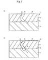
- a member 1 effective for reducing particle generationhas a substrate 2 and a surface layer 3 formed on the surface 2a of the substrate 2.
- An open pore 4communicates from the surface 3a of the surface layer 3 to the surface 2a of the substrate 2.
- 4ais an inner wall face of the open pore
- 2bis an exposed face of the substrate 2 facing the open pore.
- the open pore 4has a small pore size as described above and the layer 3 has a some thickness.
- the open porethus has an elongate shape of a relatively large aspect ratio.
- the surface layer 3is corroded as shown in a solid line shown in Fig. 1(b). Dotted lines indicate the outline of the surface layer 3 before the corrosion.
- the surface 7a of the surface layer 7is corroded, as well as the inner wall surface 6a of the open pore 6 and the exposed face 2b of the substrate 2.
- the etching rate of the substrate 2is larger than that of the surface layer 7 (susceptible to a corrosive substance)
- a relatively large hole 8is formed on the exposed face 2a of the substrate 2.
- the etched hole 8communicates with the open pore 6.
- the etching rate of the inner wall face 6a of the open pore 6is relatively small, so that the pore size of the open pore 6 is not relatively unchanged after the corrosion. Consequently, the aspect ratio of the open pore 6 (including 8) is not largely changed, or even become larger, after the corrosion (the open pore is made elongated).
- the substrate 2is more susceptible to a corrosive substance in this case. Therefore, such elongate open pore with a relatively large aspect ratio is advantageous for preventing the contact of the substrate and a corrosive substance and for preventing particle generation from the substrate.
- the substratemay be composed of a material not particularly limited.
- the materialdoes not contain an element which might adversely affect a process carried out in a container for plasma generation.
- the material of a substratemay preferably be aluminum, aluminum nitride, aluminum oxide, a compound of aluminum oxide and yttrium oxide, a solid solution of aluminum oxide and yttrium oxide, zirconium oxide, a compound of zirconium oxide and yttrium oxide, and a solid solution of zirconium oxide and yttrium oxide.
- the substrateis composed of alumina, spinel, an yttria-alumina complex oxide, zirconia or the complex oxide thereof.
- a compression forceis applied onto the surface layer after forming the layer.
- the application of the forcemay be effective for preventing particle generation from the surface layer.
- the compression forcemay be applied by a heat treatment.
- a method for controlling the " ⁇ " valueis not particularly limited.
- a mixed powder of powdery materials of yttria and aluminais sprayed onto a substrate to from a sprayed film, which is then subjected to a heat treatment, as described above.
- the powdery materialsreact with each other during the spraying step so that the volume is changed.
- Such volume changeintroduces many pores in the film.
- the crystalline phase transformationfurther proceeds so that the film shrinks to increase the open porosity and " ⁇ " value.
- Such phenomenonis found by the present inventors.
- the ⁇ " valuemay be controlled by etching using an acidic solution or plasma, particularly by etching by means of selective corrosion.
- the " ⁇ " valuemay also be controlled by recent mechanical machining processes.
- Powdery materials each having an mean particle diameter (50 percent mean particle diameter) shown in table 1were prepared among the diameters shown in table 1.
- Yttria particles(examples A1 to A3) with a mean particle diameter of 0.1, 0.5, or 5 ⁇ mare measured based on primary particles.
- the diameters of the other yttria particles(examples A4 to A8) are measured based on secondary particles.
- Alumina particles(examples A1 to A4) with a mean particle diameter of 0.1, 0.3, 4 and 20 ⁇ m are measured based on the primary particles and the other alumina particles (A5 to A8) are measured based on secondary particles.
- Alis a comparative example.
- powdery materials of yttria and aluminawere mixed in a ratio of 57.1 : 42.9 based on weight.
- the molar ratio of yttria and aluminawas 3:5.
- powdery materials of yttria and aluminawere wet mixed using a ball mill and granulated using a spray drier to obtain granules having a mean particle diameter of 40 ⁇ m.
- powdery materials of yttria and aluminawere dry mixed.
- a plate-shaped substrate made of alumina (with a purity of 99.7 percent) having a length of 50 mm, a width of 50 mm and a thickness of 2 mmwas prepared.
- the above mixed powderwas plasma sprayed on the substrate using a plasma spraying system supplied by SULZER METCO. During the spraying, argon was supplied in a flow rate of 40 liter per minute and hydrogen was supplied in a flow rate of 12 liter per minute. The power for the spraying was 40 kW, and spray distance was 120 mm.
- the peel strengthwas measured according to the following method.
- each filmwas observed using a scanning electron microscope in a magnitude of 5000.
- the sample of each examplewas set in a corrosion test system for performing the test under the following conditions. Each sample was held in Cl 2 gas (heater off) for 2 hours. The flow rate of Cl 2 gas was 300 sccm and that of a carries gas (argon gas) was 100 sccm. The gas pressure was set at 13 Pa (0.1 torr) and a power of RF 800W and a bias voltage of 310 W was applied. The weights of each sample before and after the exposure to Cl 2 gas were measured and the weight change was calculated.
- the peak strength of YAL phasewas considerably improved after the heat treatment.
- the tendencywas considerable in the examples B6, B7 and B8.
- the ratio of peak strengths YAL(420)/YAG(420)was higher than 1.5 with cracks not observed and the peel strength not considerably reduced.
- the weight gain after the corrosion testwas larger. This is due to the difference of the crystalline phases constituting the films.
- the inventionmay provide an yttria-alumina complex oxide film with a high peel strength of the film to a substrate.
- Examples C 1 to C16 shown in tables 3 and 4were produced.
- a dense alumina sintered bodywas finished by blasting using #80 abrasive grains and machined to a thickness of about 400 ⁇ m to obtain a self-standing test sample.
- YAG powder with a mean particle diameter of 40 ⁇ mwas sintered at 1600 °C or 1500 °C to produce each sintered body.
- Each sintered bodywere then finished by blasting using #80 abrasive grains and machined to a thickness of about 400 ⁇ m to obtain a self-standing test sample.
- a sprayed filmwas formed as described in the experiment A on each of two substrates.
- the substratehas a length of 150 mm, width of 150 mm and thickness of 5mm.
- the thus obtained sprayed filmwas subjected to a heat treatment in the examples C4 and C8 to C16.
- the ratio of the peak strengths, peel strength, the presence of cracks, results of corrosion resistant test, porosity, specific surface area measured by krypton adsorption method (cm 2 /g), average thickness of the film, ⁇ , volume measured by mercury penetration method, pore size and number of particleswere measured for each sample.
- the specific surface areawas measured by a Kr gas adsorption multipoint BET method.
- the bulk density of the surface layerwas set at 4 g/cm 3 .
- a porosimeter of mercury penetration systemwas used for measuring a range of pore size of 1 nm to 200 ⁇ m.
- the pore sizehas a relatively broad distribution. Therefore, each range of the pore size including main peaks were shown in table 4. 485 erg/cm 2 was applied as a surface tension value of mercury and 130 ° was applied as a contact angle.
- alumina powder used in the comparative example C1was suspended in pure water of 100 to 1000 cc.
- Each of the samples of the examples C1 to C16was immersed in the suspension and dried in atmosphere at 120 °C. The process was repeated until the suspended state was disappeared, so that almost all the alumina particles were deposited onto the coated surface layer of the test sample. Fifty times of thermal cycles between room temperature and 200 °C were applied on the sample while holding the sample with its coated surface layer directed downwardly. After the thermal cycles, particles fallen on an Si wafer set under the sample were counted.
- the samples of C1 and C2are dense sintered bodies and do not have holding capacity of particles on its surface. Many particles were thus fallen on the wafer from the sintered body. In C3, " ⁇ " was considerably increased because of insufficient sintering of YAG. Such insufficiency of sintering results in many fine open pores. In this case, even more particles were fallen after the thermal cycle. In C4, " ⁇ " of the surface layer is small and many particles were fallen. "Many particles” means approximately more than 10,000 per one wafer. In C5 to C16 according to the invention, the falling of particles on the wafer was considerably reduced. Particularly the samples of C8 to C 16 were found to be superior. It is considered that each of the samples of C8 to C16 have higher a porosity than those of C5 to C7. C11 to C16 were superior in the view point of peel strength.
- a mixed powder of powdery materials of yttria and aluminawere sprayed to produce a sprayed film in C5 to C16.
- the samples in C5, C6 and C7, the sprayed filmwas not subjected to a heat treatment and the porosity was lower than 10 percent.
- the porosity of the filmwas increased to a value higher than 10 percent as a result of a heat treatment.
- the ratio of peak strengthswere in a range of 0.05 to 1.5, the peel strength was therefore large without cracks observed.
- the present inventionmay provide a member having a capability of holding deposits firmly on the surface, so that particles due to the surface deposits may be reduced.
Landscapes
- Chemical & Material Sciences (AREA)
- Engineering & Computer Science (AREA)
- Mechanical Engineering (AREA)
- Plasma & Fusion (AREA)
- Chemical Kinetics & Catalysis (AREA)
- Materials Engineering (AREA)
- Physics & Mathematics (AREA)
- Metallurgy (AREA)
- Organic Chemistry (AREA)
- Coating By Spraying Or Casting (AREA)
- Other Surface Treatments For Metallic Materials (AREA)
- Compounds Of Alkaline-Earth Elements, Aluminum Or Rare-Earth Metals (AREA)
- Drying Of Semiconductors (AREA)
Description
- The invention relates to a film of an yttria-alumina complex oxide, a sprayed film, a corrosion-resistant member and a member effective for reducing particle generation.
- In a semiconductor manufacturing system requiring super clean state, halogen-based corrosive gases such as a chlorine-based gas and fluorine-based gas are used as a deposition gas, etching gas and cleaning gas. For example, it is used a cleaning gas for a semiconductor composed of a halogen-based corrosive gas such as ClF3, NF3, CF4, HF and HCl after a deposition stage in a semiconductor producing system such as a hot CVD system. Further, a halogen-based corrosive gas such as WF6, SiH2Cl2 or the like is used for film formation in a deposition stage.
- Further, in film-forming and etching stages of a CVD or PVD process, the chemical reaction for film formation or etching produces by-products, which are deposited onto a susceptor, electrode or parts constituting a chamber. Particularly in a system of so-called cold wall type, the chamber wall is low in the temperature, so that particles may be easily deposited onto the cold chamber wall. Although such deposits are subjected to a cleaning process of dry or wet process at a predetermined interval, too much deposits may be fallen or moved onto a semiconductor wafer, resulting in instability of semiconductor processing or reduction of a production yield.
- For preventing the falling of particles, it has been known to apply a shot peening or blast treatment using glass beads on the surface of a metal plate to increase the surface roughness, so that the retention force of the metal surface may be improved.
Kim, "Plasma-sprayed alumina-yttria ceramic coatings for cavitation-erosion protection", J. Corros. Sci. Soc. of Korea, Vol. 18, No. 3, Sept. 1989, 139-146, describes processes in which yttria and alumina powders are mixed and plasma sprayed. The amount of yttria ranges from 1 to 10 wt%. The coatings produced contain yttria and alumina, together with some yttrogarnet phases such as YAG (garnet) and YAL (perovskite).
Ullal et al., "Non-equilibrium phase synthesis in Al2O3-Y2O3 by spray pyrolysis of nitrate precursors", Acta Mater., Vol. 49, 2001, pages 2691-2699, describes processes in which solutions of yttrium nitrate and aluminium nitrate are sprayed onto aluminium to yield amorphous powders. The temperature is increased to form crystalline phases. Both YAG and YAL are formed, and alumina is present as an amorphous phase.US 2001/0003271 describes a process in which alumina and yttria are sprayed, and treated with plasma after spraying. In one case Al2O3 and Y2O3 crystals are dominant, and YAL and YAM (monoclinic) are also present. - It has been thus desired to form a film being highly resistive against a halogen-based gas or its plasma and stable for a long time period on a member used for a semiconductor-producing system, such as a member contained in the chamber or the inner wall surface of the chamber. Further, when by-products are deposited on a member contained in the system or the inner wall surface of the chamber, it is desired to hold the deposited by-products for a long time period.
- The applicant has filed a
Japanese patent application P2001-110, 136 published as JP-A-2002-249864 - An object of the present invention is to provide a film of an yttria-alumina complex oxide having a high peel strength to a substrate.
- Another object of the invention is to provide a member effective for reducing particle generation having a high retention capability of deposits and usable for a long time period with improved stability.
- Still another object of the invention is to provide a member effective for reducing particle generation having a high retention capability of deposits on the surface, so as to reduce particles due to the deposits on the member and a down time associated with maintenance of a system applying the member.
- The invention provides a film composed of yttria-alumina complex oxides as set out in
claim 1. - Further, the invention provides such a film formed by plasma spraying, the film being preferably free from a crack having a length of not smaller than 3µm and a width of not smaller than 0.1µm.
- Further, the invention provides a corrosion-resistant member comprising a substrate and the film of yttria-alumina complex oxides.
- The invention further provides a corrosion-resistant member comprising a substrate and the film composed of yttria-alumina complex oxides, which is preferably free from a crack having a length of not smaller than 3µm and a width of not smaller than 0.1 µm.
- The film may be a surface layer on the substrate. The surface layer has a value α calculated according to the following formula of not lower than 50 and not higher than 700.

- The inventors had an idea of spraying, particularly plasma spraying, a mixed powder of powdery materials of yttria and alumina on a substrate to form a sprayed film of an yttria-alumina complex oxide, and tried the process. Consequently, they have successfully formed a film having a high peel strength to a substrate with improved stability.
- The thus obtained film of yttria-alumina complex oxides does not have substantial cracks with a high peel strength to the underlying substrate, thereby preventing the peeling of the film and particle generation in contact with a corrosive substance. Additionally, when such film is subjected to a heat treatment, the peel strength of the film to the substrate may be further improved with cracks not observed in the film after the heat treatment.
Moreover, it is possible to control or regulate the microstructure of the film by controlling the conditions for the spraying process and for the heat treatment. Specifically, a porous film substantially without closed pores, or a porous film having a high ratio of open pores to closed pores may be successfully produced. A member for a semiconductor-producing system may be advantageously produced using such film and the underlying substrate. Such member has an improved specific surface area, so that deposits may be firmly hold on the surface of the member by anchor effect to reduce the thickness of the deposits on the member. It is thus possible to produce a film having a specific α value as mentioned above, which will be described later in detail. - In a preferred embodiment of the method of producing the film, the powdery material of yttria has a 50 percent mean particle diameter of not smaller than 0.1 µm and not larger than 100 µm, for further reducing the crack formation and improve the anti-corrosion property against a corrosive substance such as a halogen-based gas.
- The powdery material of yttria may preferably have a 50 percent mean particle diameter of not smaller than 0.5 µm, and more preferably not smaller than 3 µm, for further improving the adhesive strength of a film to a substrate. The 50 percent mean particle diameter of the powdery material of yttria may preferably be not larger than 80 µm, more preferably be not larger than 50 µ m and most preferably be not larger than 10µm, for further improving the adhesive strength of the film to the substrate.
- In a preferred embodiment, the powdery material of alumina may preferably has a 50 percent particle diameter of not smaller than 0.1 µm and not larger than 100 µm. It is thus possible to further reduce the crack formation and to further improve the anti-corrosion property of the film against a corrosive substance such as a halogen based gas.
- The 50 percent particle diameter of the powdery material of alumina may preferably be not smaller than 0.3 µm and more preferably be not smaller than 3 µm, for further improving the adhesive strength of the film to the substrate. The 50 percent mean particle diameter of the powdery material of alumina may preferably be not larger than 80 µm, more preferably not larger than 50 µm and most preferably not larger than 10 µm, for further improving the adhesive strength of the film to the substrate.
- The 50 percent mean particle diameter (D50) is calculated based on the diameters of primary particles when secondary particles are not observed, and the diameters of secondary particles when the secondary particles are observed, in both of the powdery materials of yttria and alumina.
- The mixed ratio of the powdery materials of yttria and alumina is not particularly limited, but should be such as to achieve the desired film. The ratio (yttria/alumina), however, may preferably be 0.2 to 1, and more preferably be 0.5 to 0.7, calculated based on the molar ratio of yttria and alumina molecules.
- The mixed powder may contain a powdery material of a third component other than yttria powder and alumina powder. It is, however, preferred that the third component does not adversely affect the crystalline phases, witch are the garnet and perovskite phases, of the yttria-alumina complex oxides, which will be described later. More preferably, the third component is a component capable of replacing the sites of yttria or alumina in the garnet or perovskite phases of an yttria-alumina complex oxide. The third component may preferably be selected from the followings.
La2O3, Pr2O3, Nd2O3, Sm2O3, Eu2O3, Gd2O3, Tb2O3, Dy2O3, Ho2O3, Er2O3, Tm2O3, Yb2O3, La2O3, MgO, CaO, SrO, ZrO2, CeO2, SiO2, Fe2O3, B2O3 - When spraying the mixed powder, the mixed powder may be sprayed on a substrate without substantially adding an additive. Alternatively, a binder and a solvent may be added to the mixed powder to produce granules by means of spray drying, and the granules may then be sprayed.
- The mixed powder may preferably be sprayed under a low pressure. The pressure may preferably be not higher than 1.3 x 10⁴ Pa (100 Torr), for further reducing the pores in the sprayed film and for enhancing the corrosion resistance of the resultant film.
- In a preferred embodiment, the sprayed film may be subjected to a heat treatment, for further improving the peel strength of the film to the substrate.
- The film may preferably be heat treated at a temperature not lower than 1300 °C and more preferably not lower than 1400 °C. It is considered that a layer of a reaction product may be formed along the interface between the substrate and film by increasing the temperature for the heat treatment not lower than 1300 °C, so that the peel strength may be improved.
- The temperature for the heat treatment has no particular upper limit, so long as the substrate is not degraded or decomposed. The temperature for the heat treatment may preferably be not higher than 2000 °C for preventing the degradation of the substrate. When the temperature for the heat treatment of the sprayed film approaches 1800 °C, aluminum elements may move and diffuse around the layer of a reaction product once formed along the interface between the film and substrate. Such movement may inversely reduce the peel strength of the corrosion-resistant film. From this point of view, the temperature for the heat treatment may preferably be not higher than 1800 °C. Further, the temperature may preferably be not higher than 1700 °C for preventing crack formation in the film.
- This film may be formed continuously over the surface of the substrate. The film, however, may be and may not be formed continuously over the entirety of a predetermined face of the substrate. For example, The film may be formed discontinuously on the surface of the substrate. The film also may be formed as a plurality of layer-like islands. In this case, such layer-like islands are not continuous to one another. Alternatively, the film may exist in a dotted manner or are scattered on a predetermined surface of the substrate.
- In a preferred embodiment, the inventive film is substantially free from cracks. Particularly, the inventive film is free from a crack having a length of not smaller than 3 µm and not smaller than 0.1 µm. The presence of such microcracks may be detected by observing a film using a scanning electron microscope applying a magnitude of not lower than 1000.
- The material of a substrate is not particularly limited. Preferably, the material does not contain an element which might adversely affect a process carried out in a container for plasma generation. From this point of view, the material of a substrate may preferably be aluminum, aluminum nitride, aluminum oxide, a compound of aluminum oxide and yttrium oxide, a solid solution of aluminum oxide and yttrium oxide, zirconium oxide, a compound of zirconium oxide and yttrium oxide, and a solid solution of zirconium oxide and yttrium oxide.
- The peel strength of the corrosion-resistant film to the substrate is measured by Sebastians test, assuming that the diameter of the bonded face is 5.2 mm.
- The substrate may be porous. The center line average surface roughness Ra of the surface of the substrate may be not smaller than 1 µm and more preferably be not smaller than 1.2 µm. It is thus possible to improve the adhesive strength of the film to the underlying substrate and to reduce the particle generation due to the peeling of the film.
- Some yttria-alumina complex oxides are the following.
- (1) Y3AL5O12 (YAG: 3Y2O3 · 5Al2O3)
This oxide contains yttria and alumina in a molar ratio of 3 : 5 and has garnet crystalline phase. - (2) YAlO3 (YAL: Y2O3 · Al2O3) perovskite crystalline phase
- (3) Y4Al2O9 (YAM: 2Y2O3 · Al2O3) monoclinic system
- In the invention, the yttria-alumina complex oxides comprise contains those of garnet and perovskite phases. The ratio YAL(420)/YAG(420) is not lower than 0.05 and not higher than 1.5. The ratio YAL(420)/YAG(420) is the ratio of a peak strength YAL (420) of the (420) face of the perovskite phase to a peak strength YAG (420) of the (420) face of the garnet phase. The peak strengths are measured by X-ray diffraction method.
- YAL(420)/YAG(420) ratio may preferably be not lower than 0.05, or not higher than 0.5
- The inventive film, or laminate of the film and a substrate, has a superior anti-corrosion property, especially against a halogen-based gas or a plasma of a halogen-based gas.
- The corrosion resistant member according to the invention may be used for a system of producing semiconductors such as thermal CVD system to make use of its anti-corrosion property. In a system for producing semiconductors, a semiconductor cleaning gas of a halogen-based corrosive gas is used. The corrosion resistant member according to the invention is corrosion resistant against a plasma of a halogen-based gas, as well as a plasma of a mixed gas of a halogen gas and oxygen gas.
- Such halogen gas includes ClF3, NF3, CF4, WF6, Cl2, BCl3 or the like.
- The invention provides a member effective for reducing particle generation comprising a substrate and a surface layer on the substrate. As mentioned, preferably the layer has a specific surface area per unit area "α" of not lower than 50 and not higher than 700.
- When generated by-products and particles deposit on the surface of the member, the deposited by-products and particles may be held in pores of the surface layer, thus preventing the falling or dispersing of the by-products and particles from the surface layer. It is thus possible to reduce defects of semiconductors due to the falling and dispersing of the particles and thereby to reduce a down time of an entire system for cleaning the deposits on the member.
- As mentioned, the specific surface area per an unit area "α" is defined according to the following formula.

- As can be seen from the above formula, "α" is a kind of index indicating a specific area per an unit surface area of a surface layer. The surface area of the surface layer may be calculated, for example, from a design drawing. More specifically, the surface area is calculated on the assumption that the surface is smooth without any irregularities formed on the surface of the layer.
- The specific surface area measured by Krypton adsorption method (cm2/g) means a specific surface area (cm2) per an unit weight (g). That is, the specific surface area means the adsorption capacity per an unit weight of a surface layer. In other words, that means the amount and diameters of open pores effective for adsorption per an unit weight of an surface layer.
- On the other hand, the thickness (cm) of a surface layer is multiplied by the bulk density of the surface layer (g/cm3) to obtain a weight per an unit surface area of the layer (g/cm2). The weight per an unit surface area of the layer (g/cm2) is then multiplied by the specific surface area measured by Krypton adsorption method (cm2/g) to obtain a specific surface area per an unit surface area (cm2/cm2), which is "α". "α" is therefore an index indicating the adsorption capacity of a gas, or the amount and diameters of open pores, per an unit surface area (1 cm2) of the surface layer. A bulk density is a density calculated by dividing a weight by a volume containing open pores and closed pores.
- "α" is preferably controlled to a value not lower than 50. A surface layer having such large specific surface area per an unit area "α" is provided on a substrate, according to the invention, so that the by-products and particles may thereby adsorbed, adhered or hold in open pores in the surface layer. It is thereby possible to reduce the falling or dispersion of particles from the surface layer. From this point of view, "α" may preferably be not larger than 100.
- When "α" is small, the surface area for holding and adsorbing the by-products is insufficient, so that the by-products deposit on the surface layer to form a thicker deposits to increase the deposits fallen from the surface layer, even when the amount of the generated by-product is not increased. Such thicker deposits increase the by-products fallen from the surface layer. Additionally, the surface area exhibits relatively poor anchor effect, so that the holding capacity of the by-products in the surface layer may be reduced.
Besides, "α" of not smaller than 50 is apparently larger than that of conventional members produced by blasting well known in a shield plate or the like used for a sputtering system (see comparative examples C1, and C2: tables 3 and 4). - When a specific surface area per an unit area "α" of the surface layer is made large, the surface area for adsorbing the by-products and particles is also increased. It may be therefore speculated that the increased "α" is advantageous for preventing the falling and dispersion of the particles and by-products. Contrary to the speculation, it is found that when "α" is beyond 700, the amount of fallen and dispersed particles is increased. The results may be explained as follows. If "α" is beyond 700, ceramic bone structure constituting the surface layer is fractured microscopically when thermal cycles are applied. Such fracture may contribute to the increase of the particles. From this point of view, "α" may preferably be not larger than 500, and more preferably be not larger than 300.
The effects, features and advantages of the invention will be appreciated upon reading the following description of the invention when taken in conjunction with the attached drawings, with the understanding that some modifications, variations and changes of the same could be made by the skilled person in the art. - Fig. 1(a) is a cross sectional view schematically showing a member effective for reducing particle generation, and
- Fig. 1(b) is a cross sectional view schematically showing the
member 1 after the corrosion. - The open porosity of the surface layer may preferably be not lower than 10 volume percent, and more preferably be not lower than 15 volume percent. It is thus possible to improve the holding capability of the by-products and particles in the surface layer. The open porosity of the surface layer may preferably be not higher than 30 volume percent. When the open porosity is higher than 30 volume percent, the corrosion resistance of the surface layer as well as the mechanical strength are reduced. The surface layer itself thus might become a source of generating particles or cracks might be introduced to increase the amount of particles.
- The ratio of the open porosity to closed porosity (open porosity/closed porosity) of the surface layer may preferably be not lower than 10. Closed pores in the surface layer do not contribute to the retention and adsorption of the by-products and particles, and may accelerate the corrosion of the layer by a corrosive substance. The ratio of the open pores may preferably be higher.
- In a preferred embodiment, the pore size of main open pores in the surface layer is 0.05 to 50 µm. It is thus possible to further improve the retention and adsorption of the by-products and particles in the open pores.
- From another point of view, the pore size of the open pores may preferably be substantially same as or larger than that according to a design rule applied for producing semiconductor devices. For example, when the design rule of the device to be produced is 0.05 µm, the pore size may preferably be not lower than 0.05 µm.
- The reasons will be described below. A wafer with fine grooves formed is stored and moved in N2 atmosphere under an atmospheric pressure. N2 and water content thus adsorb in the fine grooves formed in the wafer. When the wafer is subjected to a subsequent process such as etching or film-forming, it is necessary to remove N2 and water content adsorbed in the fine grooves of the wafer for securing the process stability. The capacity of a discharge pump and specification of discharged system (diameter of a discharge tube, flow rate of a gas or the like) of a process chamber is usually designed sufficient for removing the gas contents from the fine grooves. The design rule is an index of the width of the fine grooves formed in the wafer. When the open pores in the inventive surface layer have a pore size of the same level as the design rule, gas contents in the open pores in the surface layer may be removed using the discharge pump and system. It is therefore considered that the open pores may not adversely affect the stability of the process in the process chamber.
The pore size of the open pores in the inventive film may be substantially same as the design rule. However, the inner wall surface of a chamber usually has a surface area substantially larger than that of a wafer to be treated. When the inner wall surface is made of the inventive film, the surface area of the inventive film is much larger than that of a wafer. In this case, the pore size of the open pores in the inventive film may preferably larger than the design rule. - Further, the thickness of the surface layer may preferably be not smaller than 50 µm and more preferably be not smaller than 100 µm, for improving the retention and adsorption of the by-products and particles.
- On the other hand, the thickness of the surface layer may preferably be not larger than 1000 µm and more preferably be not larger than 400 µm, for improving the peel strength of the surface layer to the substrate and thus preventing particle generation.
- The surface layer is composed of yttria-alumina complex oxides formed by spraying a mixed powder of powdery materials of yttria and alumina on a substrate.
- In a preferred embodiment, the 50 percent mean particle diameter of the powdery material of yttria may preferably be not smaller than 0.1 µm and not larger than 100 µm. The 50 percent mean particle diameter of the powdery material of alumina may preferably be not smaller than 0.1 µm and not larger than 100 µm. The film formed by spraying may be subjected to a heat treatment. Further, the yttria-alumina complex oxide may preferably contain at least garnet phase. The yttria-alumina complex oxides comprise those of garnet and perovskite phases, and a ratio YAL (420)/YAG (420) is not smaller than 0.05 and not larger than 1.5. YAL (420) is the peak strength of the perovskite phase and YAG(420) is the peak strength of the garnet phase, both are measured by an X-ray diffraction analysis.
- The member effective for reducing particle generation is to be exposed against a corrosive substance. The corrosive substance includes the followings. A fluorocarbon such as CF4, C3F6 or the like, oxygen, chlorine, boron chloride, CHF3, CIF3, SF6, NF3, HBr, TiCl4, WF6, SiCl4, hydrogen, and the mixed gas thereof. The corrosive substance may contain a carrier gas such as He, N2 and Ar.
- The corrosive substance may preferably be the halogen gases described above and its plasmas.
- In the invention, the material of the substrate may have corrosion resistance lower than that of the material of the surface layer. The reasons will be described below. As shown in Fig. 1(a), a
member 1 effective for reducing particle generation has asubstrate 2 and asurface layer 3 formed on thesurface 2a of thesubstrate 2. Anopen pore 4 communicates from thesurface 3a of thesurface layer 3 to thesurface 2a of thesubstrate 2. 4a is an inner wall face of the open pore, and 2b is an exposed face of thesubstrate 2 facing the open pore. Theopen pore 4 has a small pore size as described above and thelayer 3 has a some thickness. The open pore thus has an elongate shape of a relatively large aspect ratio. - When the
member 1 is contacted with a corrosive substance, thesurface layer 3 is corroded as shown in a solid line shown in Fig. 1(b). Dotted lines indicate the outline of thesurface layer 3 before the corrosion. Thesurface 7a of thesurface layer 7 is corroded, as well as theinner wall surface 6a of the open pore 6 and the exposedface 2b of thesubstrate 2. When the etching rate of thesubstrate 2 is larger than that of the surface layer 7 (susceptible to a corrosive substance), a relatively large hole 8 is formed on the exposedface 2a of thesubstrate 2. The etched hole 8 communicates with the open pore 6. On the other hand, the etching rate of theinner wall face 6a of the open pore 6 is relatively small, so that the pore size of the open pore 6 is not relatively unchanged after the corrosion. Consequently, the aspect ratio of the open pore 6 (including 8) is not largely changed, or even become larger, after the corrosion (the open pore is made elongated).
Thesubstrate 2 is more susceptible to a corrosive substance in this case. Therefore, such elongate open pore with a relatively large aspect ratio is advantageous for preventing the contact of the substrate and a corrosive substance and for preventing particle generation from the substrate. - The substrate may be composed of a material not particularly limited. Preferably, the material does not contain an element which might adversely affect a process carried out in a container for plasma generation. From this point of view, the material of a substrate may preferably be aluminum, aluminum nitride, aluminum oxide, a compound of aluminum oxide and yttrium oxide, a solid solution of aluminum oxide and yttrium oxide, zirconium oxide, a compound of zirconium oxide and yttrium oxide, and a solid solution of zirconium oxide and yttrium oxide. In a particularly preferred embodiment, the substrate is composed of alumina, spinel, an yttria-alumina complex oxide, zirconia or the complex oxide thereof.
- In a preferred embodiment, a compression force is applied onto the surface layer after forming the layer. The application of the force may be effective for preventing particle generation from the surface layer. The compression force may be applied by a heat treatment.
- A method for controlling the "α" value (specific surface area per an unit area of a surface layer) is not particularly limited. Preferably, a mixed powder of powdery materials of yttria and alumina is sprayed onto a substrate to from a sprayed film, which is then subjected to a heat treatment, as described above. The powdery materials react with each other during the spraying step so that the volume is changed. Such volume change introduces many pores in the film. During the heat treatment of the sprayed film with many pores, the crystalline phase transformation further proceeds so that the film shrinks to increase the open porosity and "α" value. Such phenomenon is found by the present inventors.
- Alternatively, the α" value may be controlled by etching using an acidic solution or plasma, particularly by etching by means of selective corrosion. The "α" value may also be controlled by recent mechanical machining processes.
- Powdery materials each having an mean particle diameter (50 percent mean particle diameter) shown in table 1 were prepared among the diameters shown in table 1. Yttria particles (examples A1 to A3) with a mean particle diameter of 0.1, 0.5, or 5 µ mare measured based on primary particles. The diameters of the other yttria particles (examples A4 to A8) are measured based on secondary particles. Alumina particles (examples A1 to A4) with a mean particle diameter of 0.1, 0.3, 4 and 20 µm are measured based on the primary particles and the other alumina particles (A5 to A8) are measured based on secondary particles. Al is a comparative example.
- In the examples A1 to A8 shown in table 1, powdery materials of yttria and alumina were mixed in a ratio of 57.1 : 42.9 based on weight. The molar ratio of yttria and alumina was 3:5. In the examples A1 to A3, powdery materials of yttria and alumina were wet mixed using a ball mill and granulated using a spray drier to obtain granules having a mean particle diameter of 40 µm. In the examples A4 to A8, powdery materials of yttria and alumina were dry mixed.
- A plate-shaped substrate made of alumina (with a purity of 99.7 percent) having a length of 50 mm, a width of 50 mm and a thickness of 2 mm was prepared. The above mixed powder was plasma sprayed on the substrate using a plasma spraying system supplied by SULZER METCO. During the spraying, argon was supplied in a flow rate of 40 liter per minute and hydrogen was supplied in a flow rate of 12 liter per minute. The power for the spraying was 40 kW, and spray distance was 120 mm.
- In the example A9 (comparative example), only the powder of yttria-alumina garnet (having a mean particle diameter of 40 µm was plasma sprayed on the substrate under the conditions described above. The thus obtained films of the examples were subjected to the following measurements.
- The crystalline phases in each film were identified using an X-ray diffraction system, according to the following conditions. YAL(420)/YAG(420) was then calculated.
CuKα, 50 kV, 300 mA, 2θ = 20 to 70 °
Applied system: Rotating anode type X-ray diffraction system "RINT" supplied by "Rigaku Denki" - The peel strength was measured according to the following method.
- 1. A film-formed sample (laminate) is cut into a small test piece with a length of 10 mm, width of 10 mm and thickness of 2 mm (including the thickness of the film).
- 2. The cut piece is ultrasonically cleaned with acetone for 5 minutes.
- 3. An adhesive-provided Al stud pin (manufactured by Phototechnica Co., Ltd.) is prepared. This bonding area has a circle shape of 5.2 mm in diameter.
- 4. The pin is bonded to the film-formed side of the piece.
- 5. The pin bonded to the piece is fitted to a jig, and pulled up by an "AUTOGRAPH", manufactured by Shimadzu Co., Ltd., until the film is peeled. The bonding strength is calculated from the bonding area and the load when the film is peeled (Peel strength = peeling load/bonding area of the pin). When the peeling occurs in the adhesive, the peeling load value is not used as a result of the measurement.
- The surface of each film was observed using a scanning electron microscope in a magnitude of 5000.
- The sample of each example was set in a corrosion test system for performing the test under the following conditions. Each sample was held in Cl2 gas (heater off) for 2 hours. The flow rate of Cl2 gas was 300 sccm and that of a carries gas (argon gas) was 100 sccm. The gas pressure was set at 13 Pa (0.1 torr) and a power of RF 800W and a bias voltage of 310 W was applied. The weights of each sample before and after the exposure to Cl2 gas were measured and the weight change was calculated.
Table 1 Mean particle diameter of Y2O3 powder (µm) Mean particle diameter of Al2O3 (µm) Ratio of peak strength YAL (420) / YAG(420) Peel strength MPa Presence of Cracks Weight Gain after Corrosion test mg/hr A1* 0.1 0.1 0.000 8 None 0.0 A2 0.5 0.3 0.597 12 None 0.0 A3 5 4 0.324 30 None 0.0 A4 20 20 0.203 10 None 0.0 A5 50 50 0.108 12 None 0.1 A6 80 80 0.07 11 None 0.1 A7 100 100 0.05 10 None 0.1 A8 120 120 13 None 0.7 YAM phase observed A9* Y A G powder only (40 µm) 0.00 3 Present 1.2 * Comparative examples. - As can be seen from table 1, in the example A9, powder of yttria-alumina garnet was sprayed on the substrate and perovskite phase was not observed in the resultant sprayed film. The peel strength of the film was relatively low with cracks observed. The weight gain after the corrosion test was also large. In the examples A1 to A8, the mixed powder was sprayed. The peel strength was relatively large with cracks not observed. In particular, when the mean particle diameter of yttria powder was 0.5 to 100 µm and that of alumina powder was 0.3 to 100 µm, the peel strength was not lower than 10 MPa, cracks were not observed and the corrosion resistance was considerably higher. In A8, the mean particle diameters of powdery materials of yttria and alumina were 120 µm, respectively, with YAM phase formed. In A8, the peel strength was as high as 13 MPa with the corrosion resistance slightly reduced.
- The samples covered with the films of the examples A1 to A9 were subjected to a heat treatment, respectively, at 1500 °C for 3 hours. The thus obtained films were evaluated as the experiment A and the results were shown in table 2.
Table 2 Mean particle Diameter of Y2O3 (µm) Mean particle Diameter of Al2O3 (µm) Temperature of heat treatment (°C) Ratio of Peak strength YAL(420)/ YAG(420) Peel strength MPa Presence Of Cracks Weight gain After Corrosion test mg/hr B1* 0.1 0.1 1500 0.000 3 Present 0.7 B2 0.5 0.3 1500 0.206 43 None 0.0 B3 5 4 1500 0.258 48 None 0.0 B4 20 20 1500 0.653 52 None 0.0 B5 50 50 1500 0.996 45 None 0.1 B6 80 80 1500 1.257 48 None 0.1 B7 100 100 1500 1.385 45 None 0.1 B8 120 120 1500 1.516 40 None 0.8 B9* Y A G powder only (40µm) 1500 0.00 3 Present 1.0 * Comparative examples. - As can be seen from table 2, in the example B9, perovskite phase was not observed in the film of the example B9. The peel strength was relatively small, cracks were not found and the weight gain was large after the corrosion test. In the examples A1 to A8, the mixed powder was sprayed and the peel strength was relatively large. In the example B1, however, the reduction of the peel strength and crack formation were observed. In particular, when the particle diameter of yttria powder was 0.5 to 100 µm and the particle diameter of alumina powder was 0.3 to 100 µm, the peel strength was considerably improved to a value over 40 MPa and cracks were not observed.
- In the examples B4 to B8, the peak strength of YAL phase was considerably improved after the heat treatment. The tendency was considerable in the examples B6, B7 and B8. In the example A8, the ratio of peak strengths YAL(420)/YAG(420) was higher than 1.5 with cracks not observed and the peel strength not considerably reduced. However, the weight gain after the corrosion test was larger. This is due to the difference of the crystalline phases constituting the films.
As described above, the invention may provide an yttria-alumina complex oxide film with a high peel strength of the film to a substrate. - The members of
examples C 1 to C16 shown in tables 3 and 4 were produced. In the example C1, a dense alumina sintered body was finished by blasting using #80 abrasive grains and machined to a thickness of about 400 µm to obtain a self-standing test sample. In C2 and C3, YAG powder with a mean particle diameter of 40 µm was sintered at 1600 °C or 1500 °C to produce each sintered body. Each sintered body were then finished by blasting using #80 abrasive grains and machined to a thickness of about 400 µm to obtain a self-standing test sample. - In each of the examples C4 to C16, a sprayed film was formed as described in the experiment A on each of two substrates. The substrate has a length of 150 mm, width of 150 mm and thickness of 5mm. The thus obtained sprayed film was subjected to a heat treatment in the examples C4 and C8 to C16. The ratio of the peak strengths, peel strength, the presence of cracks, results of corrosion resistant test, porosity, specific surface area measured by krypton adsorption method (cm2/g), average thickness of the film, α, volume measured by mercury penetration method, pore size and number of particles were measured for each sample.
- The specific surface area was measured by a Kr gas adsorption multipoint BET method. The bulk density of the surface layer was set at 4 g/cm3.
- A porosimeter of mercury penetration system was used for measuring a range of pore size of 1 nm to 200 µm. The pore size has a relatively broad distribution. Therefore, each range of the pore size including main peaks were shown in table 4. 485 erg/cm2 was applied as a surface tension value of mercury and 130 ° was applied as a contact angle.
- Porosity was measured using Archimedian method. In the examples C7 to C16, it was confirmed that pores in the film was substantially composed of open pores, judging from the ratio of the bulk density and the apparent density measured by Archimedian method.
- 35 g of alumina powder used in the comparative example C1 was suspended in pure water of 100 to 1000 cc. Each of the samples of the examples C1 to C16 was immersed in the suspension and dried in atmosphere at 120 °C. The process was repeated until the suspended state was disappeared, so that almost all the alumina particles were deposited onto the coated surface layer of the test sample. Fifty times of thermal cycles between room temperature and 200 °C were applied on the sample while holding the sample with its coated surface layer directed downwardly. After the thermal cycles, particles fallen on an Si wafer set under the sample were counted.
Table 3 Production Mean particle Diameter of Y2O3 powder (µm) Mean particle diameter of Al2O3 (µm) Temperature Of heat Treatment (°C) Ratio of peak strength YAL(420) /YAG(420) Peel strength (M Pa) Presence of Cracks C1 Comparative example Sintered alumina Blast finishing - 20 Sintered at 1600°C 0 - None C2 Comparative Example Sintered alumina Blast finishing YAG powder only (40 µm) Sintered at 1600°C 0 - None C3 Comparative Example Sintered YAG YAG powder only (40 µm) Sintered at 1500°C 0 - None C4 Comparative Example Spraying of YAG synthesized Powder YAG powder only (40 µm) 1600 °C 0 4 Present C5 Example Spraying of mixed powder 20 20 No heat Treatment 0.243 10 None C6 Example Same as above 20 20 No heat Treatment 0.210 10 None C7 Example Same as above 20 20 No heat Treatment 0.195 11 None C8 Example Same as above 20 20 1400 0.597 23 None C9 Example Same as above 20 20 1400 0.541 19 None C10 Example Same as above 20 20 1400 0.553 30 None C11 Example Same as above 20 20 1600 0.803 52 None C12 Example Same as above 20 20 1600 0.784 57 None C13 Example Same as above 20 20 1600 0.792 53 None C14 Example Same as above 50 50 1600 0.732 60 None C15 Example Same as above 50 50 1600 0.718 62 None C16 Example Same as above 50 50 1600 0.696 67 None Table 4 Weight gain after Corrosion test mg/hr Porosity % Kr method cm2/g Average Thickness (µm) Ratio of Specific surface area α Volume by Mercury Penetration cc/g Range of Pore size (µm) Number of Particles C1 Comparative Example 4.7 <1 28 400 4 0.0064 - Many C2 Comparative Example 0.0 <1 9 400 1 0.0071 - Many C3 Comparative Example 1.3 10 9,317 400 1,491 0.0302 0.08-2.5 Many C4 Comparative Example 1.0 4 710 60 17 0.0147 0.004-4 Many C5 Example 0.0 5 1,173 123 58 0.0062 0.05-8 200 C6 Example 0.0 6 1,191 212 101 0.0070 0.05-8 50 C7 Example 0.0 5 1,157 430 199 0.0063 0.05-8 50 C8 Example 0.0 11 1,256 99 50 0.0111 0.05-8 0 C9 Example 0.0 13 1,192 196 93 0.0131 0.05-8 0 C10 Example 0.0 13 1,183 408 193 0.0128 0.05-8 0 C11 Example 0.0 18 1,333 110 59 0.0379 0.05-14 0 C12 Example 0.0 17 1,304 194 101 0.0390 0.05-14 0 C13 Example 0.0 18 1,298 417 217 0.0401 0.05-14 0 C14 Example 0.0 17 1,382 111 61 0.0443 0.2-20 0 C15 Example 0.0 16 1,370 220 121 0.0452 0.2-20 0 C16 Example 0.0 16 1,404 406 228 0.0493 0.2-20 0 - The samples of C1 and C2 are dense sintered bodies and do not have holding capacity of particles on its surface. Many particles were thus fallen on the wafer from the sintered body. In C3, "α" was considerably increased because of insufficient sintering of YAG. Such insufficiency of sintering results in many fine open pores. In this case, even more particles were fallen after the thermal cycle. In C4, "α" of the surface layer is small and many particles were fallen. "Many particles" means approximately more than 10,000 per one wafer. In C5 to C16 according to the invention, the falling of particles on the wafer was considerably reduced. Particularly the samples of C8 to C 16 were found to be superior. It is considered that each of the samples of C8 to C16 have higher a porosity than those of C5 to C7. C11 to C16 were superior in the view point of peel strength.
- Among the inventive examples, a mixed powder of powdery materials of yttria and alumina were sprayed to produce a sprayed film in C5 to C16. The samples in C5, C6 and C7, the sprayed film was not subjected to a heat treatment and the porosity was lower than 10 percent. In the samples of C8 to C16, the porosity of the film was increased to a value higher than 10 percent as a result of a heat treatment.
- Moreover, in the samples of C5 to C16, the ratio of peak strengths were in a range of 0.05 to 1.5, the peel strength was therefore large without cracks observed.
- As described above, the present invention may provide a member having a capability of holding deposits firmly on the surface, so that particles due to the surface deposits may be reduced.


Claims (12)
- A film composed of yttria-alumina complex oxides, wherein said yttria-alumina complex oxides comprise those of garnet (YAG) and perovskite (YAL) phases and the ratio YAL(420)/YAG(420) is not lower than 0.05 and not higher than 1.5, said ratio YAL(420)/YAG(420) being the ratio of the peak strength YAL (420) of the (420) plane of said perovskite phase to the peak strength YAG (420) of the (420) plane of said garnet phase, said peak strengths being measured by x-ray diffraction.
- A film according to claim 1 which has, in addition to said garnet (YAG) and perovskite (YAL) phases, also the monoclinic phase (YAM).
- The film of claim 1 or 2, which is free from a crack having a length of not smaller than 3 µm and a width of not smaller than 0.1 µm.
- The film of claim 1, 2 or 3 formed by plasma spraying.
- A corrosion-resistant member comprising a substrate and a film composed of yttria-alumina complex oxides according to any one of claims 1 to 4.
- The member of claim 5, wherein the peeling strength of said film to said substrate is not lower than 10 MPa.
- The member according to claim 5 or 6, wherein said film is a surface layer on said substrate, and said surface layer has a value a calculated according to the following formula of not lower than 50 and not higher than 700:-


- The member of claim 7, wherein said surface layer has an open porosity of not lower than 10 volume percent and not higher than 30 volume percent.
- The member of claim 7 or 8, wherein said surface layer has a ratio of an open porosity to a closed porosity (open porosity/closed porosity) of not higher than 10.
- The member of any one of claims 7 to 9, wherein said surface layer has a pore diameter of main open pores of 0.05 to 50 µm.
- The member of any one of claims 7 to 10, wherein said surface layer has a thickness of not smaller than 50 µm.
- Use of the corrosion-resistant member of any one of claims 1 to 11, wherein said member is exposed to a halogen gas or a plasma of a halogen gas.


Applications Claiming Priority (4)
| Application Number | Priority Date | Filing Date | Title |
|---|---|---|---|
| JP2001219092 | 2001-07-19 | ||
| JP2001219092 | 2001-07-19 | ||
| JP2002180769 | 2002-06-21 | ||
| JP2002180769AJP4277973B2 (en) | 2001-07-19 | 2002-06-21 | Yttria-alumina composite oxide film production method, yttria-alumina composite oxide film, and corrosion-resistant member |
Publications (3)
| Publication Number | Publication Date |
|---|---|
| EP1277850A2 EP1277850A2 (en) | 2003-01-22 |
| EP1277850A3 EP1277850A3 (en) | 2003-11-12 |
| EP1277850B1true EP1277850B1 (en) | 2007-09-12 |
Family
ID=26618975
Family Applications (1)
| Application Number | Title | Priority Date | Filing Date |
|---|---|---|---|
| EP20020255011Expired - LifetimeEP1277850B1 (en) | 2001-07-19 | 2002-07-16 | Sprayed film of yttria-alumina complex oxide |
Country Status (6)
| Country | Link |
|---|---|
| US (2) | US6641941B2 (en) |
| EP (1) | EP1277850B1 (en) |
| JP (1) | JP4277973B2 (en) |
| KR (1) | KR100489172B1 (en) |
| DE (1) | DE60222341T2 (en) |
| TW (1) | TWI232174B (en) |
Families Citing this family (78)
| Publication number | Priority date | Publication date | Assignee | Title |
|---|---|---|---|---|
| JP4277973B2 (en)* | 2001-07-19 | 2009-06-10 | 日本碍子株式会社 | Yttria-alumina composite oxide film production method, yttria-alumina composite oxide film, and corrosion-resistant member |
| JP4663927B2 (en)* | 2001-08-29 | 2011-04-06 | 信越化学工業株式会社 | Rare earth-containing oxide member |
| US20080213496A1 (en)* | 2002-02-14 | 2008-09-04 | Applied Materials, Inc. | Method of coating semiconductor processing apparatus with protective yttrium-containing coatings |
| US8067067B2 (en)* | 2002-02-14 | 2011-11-29 | Applied Materials, Inc. | Clean, dense yttrium oxide coating protecting semiconductor processing apparatus |
| JP2003277051A (en)* | 2002-03-22 | 2003-10-02 | Ngk Insulators Ltd | Multilayer body having yttria - alumina compound oxide film, yttria - alumina compound oxide film, corrosion- resistant member, corrosion-resistant film and method for manufacturing yttria - alumina compound oxide film |
| US7250220B1 (en)* | 2002-10-03 | 2007-07-31 | Tosoh Set, Inc. | Bond strength of coatings to ceramic components |
| DE10257554B4 (en)* | 2002-12-10 | 2008-04-10 | Treibacher Schleifmittel Gmbh | Abrasive grains coated with an aqueous binder and a complex fine oxide compound, methods for treating such abrasive grains, and their use for resin bonded abrasives |
| JP4208580B2 (en)* | 2003-01-15 | 2009-01-14 | 日本碍子株式会社 | Composite sintered body and manufacturing method thereof |
| JP2005008483A (en)* | 2003-06-19 | 2005-01-13 | Shin Etsu Chem Co Ltd | Covering member and manufacturing method thereof |
| JP2005041746A (en)* | 2003-07-24 | 2005-02-17 | Ngk Insulators Ltd | Ceramic sintered compact |
| US7329467B2 (en)* | 2003-08-22 | 2008-02-12 | Saint-Gobain Ceramics & Plastics, Inc. | Ceramic article having corrosion-resistant layer, semiconductor processing apparatus incorporating same, and method for forming same |
| US20050048788A1 (en)* | 2003-08-26 | 2005-03-03 | Tang Woody K. Sattayapiwat | Methods of reducing or removing micromasking residue prior to metal etch using oxide hardmask |
| US7220497B2 (en)* | 2003-12-18 | 2007-05-22 | Lam Research Corporation | Yttria-coated ceramic components of semiconductor material processing apparatuses and methods of manufacturing the components |
| US20060165994A1 (en)* | 2004-07-07 | 2006-07-27 | General Electric Company | Protective coating on a substrate and method of making thereof |
| WO2006043429A1 (en)* | 2004-10-18 | 2006-04-27 | Nihon Ceratec Co., Ltd. | Corrosion-resistant member and method for manufacture thereof |
| JP5137304B2 (en)* | 2004-10-18 | 2013-02-06 | 株式会社日本セラテック | Corrosion resistant member and manufacturing method thereof |
| JP4666575B2 (en)* | 2004-11-08 | 2011-04-06 | 東京エレクトロン株式会社 | Manufacturing method of ceramic sprayed member, program for executing the method, storage medium, and ceramic sprayed member |
| JP4560387B2 (en) | 2004-11-30 | 2010-10-13 | 株式会社フジミインコーポレーテッド | Thermal spray powder, thermal spraying method and thermal spray coating |
| JP4912598B2 (en)* | 2005-02-15 | 2012-04-11 | 株式会社フジミインコーポレーテッド | Thermal spray powder |
| JP4680681B2 (en)* | 2005-04-26 | 2011-05-11 | 株式会社日本セラテック | Corrosion resistant member and manufacturing method thereof |
| WO2007023971A1 (en)* | 2005-08-22 | 2007-03-01 | Tocalo Co., Ltd. | Structural member coated with spray coating film excellent in thermal emission properties and the like, and method for production thereof |
| US8231986B2 (en)* | 2005-08-22 | 2012-07-31 | Tocalo Co., Ltd. | Spray coating member having excellent injury resistance and so on and method for producing the same |
| JP4571561B2 (en) | 2005-09-08 | 2010-10-27 | トーカロ株式会社 | Thermal spray coating coated member having excellent plasma erosion resistance and method for producing the same |
| JP5089874B2 (en)* | 2005-09-12 | 2012-12-05 | トーカロ株式会社 | Plasma processing apparatus member and manufacturing method thereof |
| JP4981292B2 (en)* | 2005-09-30 | 2012-07-18 | 株式会社フジミインコーポレーテッド | Thermal spray powder and method of forming thermal spray coating |
| US8075860B2 (en) | 2005-09-30 | 2011-12-13 | Fujimi Incorporated | Thermal spray powder and method for forming a thermal spray coating |
| JP2007126712A (en)* | 2005-11-02 | 2007-05-24 | Fujimi Inc | Powder for thermal spraying and method for forming thermally sprayed coating |
| US20090239061A1 (en)* | 2006-11-08 | 2009-09-24 | General Electric Corporation | Ceramic corrosion resistant coating for oxidation resistance |
| US10242888B2 (en) | 2007-04-27 | 2019-03-26 | Applied Materials, Inc. | Semiconductor processing apparatus with a ceramic-comprising surface which exhibits fracture toughness and halogen plasma resistance |
| US10622194B2 (en) | 2007-04-27 | 2020-04-14 | Applied Materials, Inc. | Bulk sintered solid solution ceramic which exhibits fracture toughness and halogen plasma resistance |
| KR100863456B1 (en) | 2008-01-14 | 2008-11-18 | 주식회사 코미코 | Spray coating powder and spray coating powder manufacturing method |
| US20090214825A1 (en)* | 2008-02-26 | 2009-08-27 | Applied Materials, Inc. | Ceramic coating comprising yttrium which is resistant to a reducing plasma |
| US20090261065A1 (en)* | 2008-04-18 | 2009-10-22 | Lam Research Corporation | Components for use in a plasma chamber having reduced particle generation and method of making |
| US8449993B2 (en)* | 2009-08-31 | 2013-05-28 | General Electric Company | Wetting resistant materials and articles made therewith |
| US20110086163A1 (en)* | 2009-10-13 | 2011-04-14 | Walbar Inc. | Method for producing a crack-free abradable coating with enhanced adhesion |
| WO2011049938A2 (en)* | 2009-10-20 | 2011-04-28 | Saint-Gobain Ceramics & Plastics, Inc. | Microelectronic processing component having a corrosion-resistant layer, microelectronic workpiece processing apparatus incorporating same, and method of forming an article having the corrosion-resistant layer |
| TW201334035A (en)* | 2011-10-06 | 2013-08-16 | Greene Tweed Of Delaware | Plasma etch resistant films, articles bearing plasma etch resistant films and related methods |
| JP2013095973A (en)* | 2011-11-02 | 2013-05-20 | Tocalo Co Ltd | Member for semiconductor manufacturing device |
| TW201418190A (en)* | 2012-07-06 | 2014-05-16 | Tocalo Co Ltd | Carbon material having thermal sprayed coating layer |
| US20140141173A1 (en)* | 2012-11-16 | 2014-05-22 | General Electric Company | Method of applying a coating to a perforated substrate |
| US9708713B2 (en) | 2013-05-24 | 2017-07-18 | Applied Materials, Inc. | Aerosol deposition coating for semiconductor chamber components |
| US9865434B2 (en)* | 2013-06-05 | 2018-01-09 | Applied Materials, Inc. | Rare-earth oxide based erosion resistant coatings for semiconductor application |
| US9583369B2 (en) | 2013-07-20 | 2017-02-28 | Applied Materials, Inc. | Ion assisted deposition for rare-earth oxide based coatings on lids and nozzles |
| US9440886B2 (en) | 2013-11-12 | 2016-09-13 | Applied Materials, Inc. | Rare-earth oxide based monolithic chamber material |
| US9725799B2 (en) | 2013-12-06 | 2017-08-08 | Applied Materials, Inc. | Ion beam sputtering with ion assisted deposition for coatings on chamber components |
| US10196728B2 (en)* | 2014-05-16 | 2019-02-05 | Applied Materials, Inc. | Plasma spray coating design using phase and stress control |
| KR102437125B1 (en)* | 2014-06-27 | 2022-08-25 | 어플라이드 머티어리얼스, 인코포레이티드 | Plasma corrosion resistive heater for high temperature processing |
| JP6156446B2 (en)* | 2014-09-29 | 2017-07-05 | 住友大阪セメント株式会社 | Corrosion-resistant member, electrostatic chuck member, and method of manufacturing corrosion-resistant member |
| CN105500823A (en)* | 2014-10-15 | 2016-04-20 | 深圳富泰宏精密工业有限公司 | Preparation method of complex of metal and resin |
| CN105624602B (en)* | 2014-10-28 | 2018-11-02 | 北京美桥电子设备有限公司 | Y applied to aluminum-based base material3Al5O12Method for producing a coating |
| JP6670625B2 (en)* | 2015-07-10 | 2020-03-25 | 東京エレクトロン株式会社 | Plasma processing apparatus and shower head |
| JP6005314B1 (en)* | 2016-03-25 | 2016-10-12 | リバストン工業株式会社 | Film-coated substrate, plasma etching apparatus component, and manufacturing method thereof |
| US11326253B2 (en) | 2016-04-27 | 2022-05-10 | Applied Materials, Inc. | Atomic layer deposition of protective coatings for semiconductor process chamber components |
| EP3471959B1 (en)* | 2016-06-15 | 2022-04-06 | The Penn State Research Foundation | Thermal barrier coatings |
| US9850573B1 (en) | 2016-06-23 | 2017-12-26 | Applied Materials, Inc. | Non-line of sight deposition of erbium based plasma resistant ceramic coating |
| US20180016678A1 (en) | 2016-07-15 | 2018-01-18 | Applied Materials, Inc. | Multi-layer coating with diffusion barrier layer and erosion resistant layer |
| KR101920002B1 (en)* | 2016-11-17 | 2018-11-19 | 금오공과대학교 산학협력단 | Coatable glass frit composition and the manufacturing method of coating layer for plasma sustaining ceramics |
| US10186400B2 (en) | 2017-01-20 | 2019-01-22 | Applied Materials, Inc. | Multi-layer plasma resistant coating by atomic layer deposition |
| US10755900B2 (en) | 2017-05-10 | 2020-08-25 | Applied Materials, Inc. | Multi-layer plasma erosion protection for chamber components |
| JP6893121B2 (en)* | 2017-05-29 | 2021-06-23 | 日立造船株式会社 | Method of manufacturing thermal spraying material, thermal spraying material and thermal spraying method |
| KR101981387B1 (en)* | 2017-06-13 | 2019-05-22 | 강동원 | A Method for Producing a Remote Plasma Source Block with a Coated Surface and the Surface-Coated Remote Plasma Source Block by the Same |
| US11279656B2 (en) | 2017-10-27 | 2022-03-22 | Applied Materials, Inc. | Nanopowders, nanoceramic materials and methods of making and use thereof |
| KR102395660B1 (en)* | 2017-12-19 | 2022-05-10 | (주)코미코 | Powder for thermal spray and thermal spray coating using the same |
| TWI714965B (en) | 2018-02-15 | 2021-01-01 | 日商京瓷股份有限公司 | Member for plasma processing device and plasma processing device with same |
| US10443126B1 (en) | 2018-04-06 | 2019-10-15 | Applied Materials, Inc. | Zone-controlled rare-earth oxide ALD and CVD coatings |
| US11667575B2 (en) | 2018-07-18 | 2023-06-06 | Applied Materials, Inc. | Erosion resistant metal oxide coatings |
| US11180847B2 (en) | 2018-12-06 | 2021-11-23 | Applied Materials, Inc. | Atomic layer deposition coatings for high temperature ceramic components |
| CN109680241B (en)* | 2019-02-26 | 2020-10-23 | 中国科学院上海硅酸盐研究所 | Preparation method of amorphous oxide ceramic composite coating integrated with toughness, thermal conductivity and high temperature microstructure stability |
| US10858741B2 (en) | 2019-03-11 | 2020-12-08 | Applied Materials, Inc. | Plasma resistant multi-layer architecture for high aspect ratio parts |
| JP7331762B2 (en)* | 2019-04-12 | 2023-08-23 | 信越化学工業株式会社 | Thermal spray material, method for producing same, and method for forming thermal spray coating |
| WO2020217552A1 (en)* | 2019-04-26 | 2020-10-29 | 日本イットリウム株式会社 | Powder for film formation or sintering |
| KR102669394B1 (en) | 2019-04-26 | 2024-05-28 | 닛폰 이트륨 가부시키가이샤 | Powder for film forming or sintering |
| FR3103191A1 (en)* | 2019-11-15 | 2021-05-21 | Centre National De La Recherche Scientifique | SOL-GEL PROCESS FOR MANUFACTURING A PRECURSOR GEL, A XEROGEL AND A YTTRIUM AND ALUMINUM GARNET POWDER AND THEIR USE TO FORM ARTICLES |
| CN112899617B (en) | 2019-12-04 | 2023-03-31 | 中微半导体设备(上海)股份有限公司 | Method, device, component and plasma processing device for forming plasma-resistant coating |
| JP2023511102A (en)* | 2020-01-23 | 2023-03-16 | ラム リサーチ コーポレーション | Yttrium aluminum coating for plasma processing chamber components |
| KR102290498B1 (en) | 2020-03-30 | 2021-08-17 | (주)도 은 | Low refractrive index substance containing oxyittirum fluoride for coating film of lens and process for preparing the same |
| WO2021229914A1 (en)* | 2020-05-12 | 2021-11-18 | 日本イットリウム株式会社 | Powder for film formation or sintering |
| CN112410719B (en)* | 2020-10-20 | 2023-01-20 | 安徽华飞机械铸锻有限公司 | Wear-resistant heat-resistant steel |
Family Cites Families (12)
| Publication number | Priority date | Publication date | Assignee | Title |
|---|---|---|---|---|
| CA1004964A (en) | 1972-05-30 | 1977-02-08 | Union Carbide Corporation | Corrosion resistant coatings and process for making the same |
| US5008221A (en)* | 1985-04-11 | 1991-04-16 | Corning Incorporated | High toughness ceramic alloys |
| JPS6379777A (en)* | 1986-09-24 | 1988-04-09 | 科学技術庁金属材料技術研究所長 | Method for manufacturing coatings on ceramic substrates |
| JPH08290977A (en)* | 1995-04-19 | 1996-11-05 | Showa Denko Kk | Thermal spraying material |
| KR20010062209A (en)* | 1999-12-10 | 2001-07-07 | 히가시 데쓰로 | Processing apparatus with a chamber having therein a high-etching resistant sprayed film |
| US6410471B2 (en)* | 2000-03-07 | 2002-06-25 | Shin-Etsu Chemical Co., Ltd. | Method for preparation of sintered body of rare earth oxide |
| TW503449B (en) | 2000-04-18 | 2002-09-21 | Ngk Insulators Ltd | Halogen gas plasma-resistive members and method for producing the same, laminates, and corrosion-resistant members |
| JP4277973B2 (en)* | 2001-07-19 | 2009-06-10 | 日本碍子株式会社 | Yttria-alumina composite oxide film production method, yttria-alumina composite oxide film, and corrosion-resistant member |
| JP2003277051A (en)* | 2002-03-22 | 2003-10-02 | Ngk Insulators Ltd | Multilayer body having yttria - alumina compound oxide film, yttria - alumina compound oxide film, corrosion- resistant member, corrosion-resistant film and method for manufacturing yttria - alumina compound oxide film |
| TWI241284B (en)* | 2002-06-06 | 2005-10-11 | Ngk Insulators Ltd | A method of producing sintered bodies, a method of producing shaped bodies, shaped bodies, corrosion resistant members and a method of producing ceramic member |
| JP2005026593A (en)* | 2003-05-08 | 2005-01-27 | Ngk Insulators Ltd | Ceramic product, corrosion-resistant member, and method of manufacturing ceramic product |
| JP2005041746A (en)* | 2003-07-24 | 2005-02-17 | Ngk Insulators Ltd | Ceramic sintered compact |
- 2002
- 2002-06-21JPJP2002180769Apatent/JP4277973B2/ennot_activeExpired - Lifetime
- 2002-06-26TWTW91114037Apatent/TWI232174B/ennot_activeIP Right Cessation
- 2002-07-16DEDE2002622341patent/DE60222341T2/ennot_activeExpired - Lifetime
- 2002-07-16EPEP20020255011patent/EP1277850B1/ennot_activeExpired - Lifetime
- 2002-07-17USUS10/197,037patent/US6641941B2/ennot_activeExpired - Lifetime
- 2002-07-18KRKR10-2002-0041895Apatent/KR100489172B1/ennot_activeExpired - Lifetime
- 2003
- 2003-08-04USUS10/633,906patent/US7138192B2/ennot_activeExpired - Lifetime
Also Published As
| Publication number | Publication date |
|---|---|
| EP1277850A3 (en) | 2003-11-12 |
| DE60222341D1 (en) | 2007-10-25 |
| US6641941B2 (en) | 2003-11-04 |
| JP2003095649A (en) | 2003-04-03 |
| US20030059653A1 (en) | 2003-03-27 |
| EP1277850A2 (en) | 2003-01-22 |
| KR100489172B1 (en) | 2005-05-17 |
| JP4277973B2 (en) | 2009-06-10 |
| KR20030009186A (en) | 2003-01-29 |
| DE60222341T2 (en) | 2008-06-19 |
| US7138192B2 (en) | 2006-11-21 |
| US20040067392A1 (en) | 2004-04-08 |
| TWI232174B (en) | 2005-05-11 |
Similar Documents
| Publication | Publication Date | Title |
|---|---|---|
| EP1277850B1 (en) | Sprayed film of yttria-alumina complex oxide | |
| EP3443136B1 (en) | Coated semiconductor processing members having chlorine and fluorine plasma erosion resistance and complex oxide coatings therefor | |
| CN112779488B (en) | Yttrium fluoride spray coating, spray material therefor, and corrosion-resistant coating comprising spray coating | |
| US11373882B2 (en) | Coated article and semiconductor chamber apparatus formed from yttrium oxide and zirconium oxide | |
| CN101293771B (en) | Apparatus and method for reducing the rate of corrosion of surfaces exposed to halogen-containing plasmas | |
| TWI483291B (en) | Method and apparatus which reduce the erosion rate of surfaces exposed to halogen-containing plasmas | |
| US6858332B2 (en) | Yttria-alumina composite oxide films, laminated bodies having the same, a method for producing the same, and corrosion resistant members and films | |
| JP2002249864A (en) | Halogen gas plasma resistant member and production method therefor | |
| JP7306490B2 (en) | Yttrium fluoride-based thermal spray coating, thermal sprayed member, and method for producing yttrium fluoride-based thermal spray coating | |
| JP2005097685A (en) | Corrosion resistant member and manufacturing method thereof | |
| US6670294B2 (en) | Corrosion-resistive ceramic materials and members for semiconductor manufacturing | |
| JP3784180B2 (en) | Corrosion resistant material | |
| JPH11102900A (en) | Corrosion resistant materials for semiconductor manufacturing | |
| JP2025124277A (en) | Plasma-resistant materials | |
| KR20240145684A (en) | Coating method for workpieces of MLCC inspection equipment | |
| JP2001097790A (en) | Corrosionproof member and method for producing the same |
Legal Events
| Date | Code | Title | Description |
|---|---|---|---|
| PUAI | Public reference made under article 153(3) epc to a published international application that has entered the european phase | Free format text:ORIGINAL CODE: 0009012 | |
| AK | Designated contracting states | Kind code of ref document:A2 Designated state(s):AT BE BG CH CY CZ DE DK EE ES FI FR GB GR IE IT LI LU MC NL PT SE SK TR | |
| AX | Request for extension of the european patent | Free format text:AL;LT;LV;MK;RO;SI | |
| PUAL | Search report despatched | Free format text:ORIGINAL CODE: 0009013 | |
| RIC1 | Information provided on ipc code assigned before grant | Ipc:7C 23C 4/18 B Ipc:7C 23C 4/10 A | |
| AK | Designated contracting states | Kind code of ref document:A3 Designated state(s):AT BE BG CH CY CZ DE DK EE ES FI FR GB GR IE IT LI LU MC NL PT SE SK TR | |
| AX | Request for extension of the european patent | Extension state:AL LT LV MK RO SI | |
| 17P | Request for examination filed | Effective date:20040416 | |
| AKX | Designation fees paid | Designated state(s):DE FR GB | |
| GRAP | Despatch of communication of intention to grant a patent | Free format text:ORIGINAL CODE: EPIDOSNIGR1 | |
| RTI1 | Title (correction) | Free format text:SPRAYED FILM OF YTTRIA-ALUMINA COMPLEX OXIDE | |
| GRAS | Grant fee paid | Free format text:ORIGINAL CODE: EPIDOSNIGR3 | |
| GRAA | (expected) grant | Free format text:ORIGINAL CODE: 0009210 | |
| AK | Designated contracting states | Kind code of ref document:B1 Designated state(s):DE FR GB | |
| REG | Reference to a national code | Ref country code:GB Ref legal event code:FG4D | |
| REF | Corresponds to: | Ref document number:60222341 Country of ref document:DE Date of ref document:20071025 Kind code of ref document:P | |
| ET | Fr: translation filed | ||
| PLBE | No opposition filed within time limit | Free format text:ORIGINAL CODE: 0009261 | |
| STAA | Information on the status of an ep patent application or granted ep patent | Free format text:STATUS: NO OPPOSITION FILED WITHIN TIME LIMIT | |
| 26N | No opposition filed | Effective date:20080613 | |
| REG | Reference to a national code | Ref country code:FR Ref legal event code:PLFP Year of fee payment:15 | |
| REG | Reference to a national code | Ref country code:FR Ref legal event code:PLFP Year of fee payment:16 | |
| REG | Reference to a national code | Ref country code:FR Ref legal event code:PLFP Year of fee payment:17 | |
| PGFP | Annual fee paid to national office [announced via postgrant information from national office to epo] | Ref country code:FR Payment date:20200611 Year of fee payment:19 | |
| PGFP | Annual fee paid to national office [announced via postgrant information from national office to epo] | Ref country code:GB Payment date:20200708 Year of fee payment:19 Ref country code:DE Payment date:20200630 Year of fee payment:19 | |
| REG | Reference to a national code | Ref country code:DE Ref legal event code:R119 Ref document number:60222341 Country of ref document:DE | |
| GBPC | Gb: european patent ceased through non-payment of renewal fee | Effective date:20210716 | |
| PG25 | Lapsed in a contracting state [announced via postgrant information from national office to epo] | Ref country code:GB Free format text:LAPSE BECAUSE OF NON-PAYMENT OF DUE FEES Effective date:20210716 Ref country code:DE Free format text:LAPSE BECAUSE OF NON-PAYMENT OF DUE FEES Effective date:20220201 | |
| PG25 | Lapsed in a contracting state [announced via postgrant information from national office to epo] | Ref country code:FR Free format text:LAPSE BECAUSE OF NON-PAYMENT OF DUE FEES Effective date:20210731 |