EP1266428B1 - Dielectric resonator antenna array with steerable elements - Google Patents
Dielectric resonator antenna array with steerable elementsDownload PDFInfo
- Publication number
- EP1266428B1 EP1266428B1EP01915468AEP01915468AEP1266428B1EP 1266428 B1EP1266428 B1EP 1266428B1EP 01915468 AEP01915468 AEP 01915468AEP 01915468 AEP01915468 AEP 01915468AEP 1266428 B1EP1266428 B1EP 1266428B1
- Authority
- EP
- European Patent Office
- Prior art keywords
- array
- elements
- dielectric resonator
- dielectric
- feeds
- Prior art date
- Legal status (The legal status is an assumption and is not a legal conclusion. Google has not performed a legal analysis and makes no representation as to the accuracy of the status listed.)
- Expired - Lifetime
Links
- 239000000758substrateSubstances0.000claimsabstractdescription18
- 239000000523sampleSubstances0.000claimsdescription40
- 230000005540biological transmissionEffects0.000claimsdescription27
- 239000003989dielectric materialSubstances0.000claimsdescription15
- 238000003491arrayMethods0.000claimsdescription9
- 230000007246mechanismEffects0.000claimsdescription9
- 230000001934delayEffects0.000claimsdescription8
- 239000000463materialSubstances0.000claimsdescription7
- 230000015572biosynthetic processEffects0.000claimsdescription6
- 150000001875compoundsChemical class0.000claimsdescription6
- 239000007787solidSubstances0.000claimsdescription6
- 239000000835fiberSubstances0.000claimsdescription2
- 230000001788irregularEffects0.000claimsdescription2
- 239000007788liquidSubstances0.000claimsdescription2
- 238000012986modificationMethods0.000claimsdescription2
- 230000004048modificationEffects0.000claimsdescription2
- 230000010363phase shiftEffects0.000claimsdescription2
- 229910000859α-FeInorganic materials0.000claimsdescription2
- 239000011343solid materialSubstances0.000claims1
- 239000012071phaseSubstances0.000description16
- 230000005855radiationEffects0.000description16
- 230000005404monopoleEffects0.000description10
- 238000000034methodMethods0.000description8
- 230000008901benefitEffects0.000description6
- 239000011159matrix materialSubstances0.000description6
- 238000004891communicationMethods0.000description3
- 230000000694effectsEffects0.000description3
- 230000005284excitationEffects0.000description3
- 230000004913activationEffects0.000description2
- 238000012937correctionMethods0.000description2
- 230000008878couplingEffects0.000description2
- 238000010168coupling processMethods0.000description2
- 238000005859coupling reactionMethods0.000description2
- 238000013461designMethods0.000description2
- 230000006872improvementEffects0.000description2
- 230000008569processEffects0.000description2
- 238000012545processingMethods0.000description2
- NKJOXAZJBOMXID-UHFFFAOYSA-N1,1'-OxybisoctaneChemical compoundCCCCCCCCOCCCCCCCCNKJOXAZJBOMXID-UHFFFAOYSA-N0.000description1
- 239000000919ceramicSubstances0.000description1
- 230000005670electromagnetic radiationEffects0.000description1
- 239000007792gaseous phaseSubstances0.000description1
- 230000006698inductionEffects0.000description1
- 238000003780insertionMethods0.000description1
- 230000037431insertionEffects0.000description1
- 238000002955isolationMethods0.000description1
- 239000007791liquid phaseSubstances0.000description1
- 238000005259measurementMethods0.000description1
- 238000010295mobile communicationMethods0.000description1
- 230000003287optical effectEffects0.000description1
- 230000003094perturbing effectEffects0.000description1
- 238000011084recoveryMethods0.000description1
- 230000009467reductionEffects0.000description1
- 238000011160researchMethods0.000description1
- 238000012552reviewMethods0.000description1
- 230000035945sensitivityEffects0.000description1
- 238000000926separation methodMethods0.000description1
- 239000007790solid phaseSubstances0.000description1
- 230000001360synchronised effectEffects0.000description1
- 230000009897systematic effectEffects0.000description1
- 238000012360testing methodMethods0.000description1
Images
Classifications
- H—ELECTRICITY
- H01—ELECTRIC ELEMENTS
- H01Q—ANTENNAS, i.e. RADIO AERIALS
- H01Q19/00—Combinations of primary active antenna elements and units with secondary devices, e.g. with quasi-optical devices, for giving the antenna a desired directional characteristic
- H01Q19/06—Combinations of primary active antenna elements and units with secondary devices, e.g. with quasi-optical devices, for giving the antenna a desired directional characteristic using refracting or diffracting devices, e.g. lens
- H01Q19/09—Combinations of primary active antenna elements and units with secondary devices, e.g. with quasi-optical devices, for giving the antenna a desired directional characteristic using refracting or diffracting devices, e.g. lens wherein the primary active element is coated with or embedded in a dielectric or magnetic material
- H—ELECTRICITY
- H01—ELECTRIC ELEMENTS
- H01Q—ANTENNAS, i.e. RADIO AERIALS
- H01Q19/00—Combinations of primary active antenna elements and units with secondary devices, e.g. with quasi-optical devices, for giving the antenna a desired directional characteristic
- H01Q19/10—Combinations of primary active antenna elements and units with secondary devices, e.g. with quasi-optical devices, for giving the antenna a desired directional characteristic using reflecting surfaces
- H01Q19/106—Combinations of primary active antenna elements and units with secondary devices, e.g. with quasi-optical devices, for giving the antenna a desired directional characteristic using reflecting surfaces using two or more intersecting plane surfaces, e.g. corner reflector antennas
- H—ELECTRICITY
- H01—ELECTRIC ELEMENTS
- H01Q—ANTENNAS, i.e. RADIO AERIALS
- H01Q21/00—Antenna arrays or systems
- H01Q21/06—Arrays of individually energised antenna units similarly polarised and spaced apart
- H—ELECTRICITY
- H01—ELECTRIC ELEMENTS
- H01Q—ANTENNAS, i.e. RADIO AERIALS
- H01Q3/00—Arrangements for changing or varying the orientation or the shape of the directional pattern of the waves radiated from an antenna or antenna system
- H01Q3/24—Arrangements for changing or varying the orientation or the shape of the directional pattern of the waves radiated from an antenna or antenna system varying the orientation by switching energy from one active radiating element to another, e.g. for beam switching
- H—ELECTRICITY
- H01—ELECTRIC ELEMENTS
- H01Q—ANTENNAS, i.e. RADIO AERIALS
- H01Q3/00—Arrangements for changing or varying the orientation or the shape of the directional pattern of the waves radiated from an antenna or antenna system
- H01Q3/26—Arrangements for changing or varying the orientation or the shape of the directional pattern of the waves radiated from an antenna or antenna system varying the relative phase or relative amplitude of energisation between two or more active radiating elements; varying the distribution of energy across a radiating aperture
- H—ELECTRICITY
- H01—ELECTRIC ELEMENTS
- H01Q—ANTENNAS, i.e. RADIO AERIALS
- H01Q9/00—Electrically-short antennas having dimensions not more than twice the operating wavelength and consisting of conductive active radiating elements
- H01Q9/04—Resonant antennas
- H01Q9/0485—Dielectric resonator antennas
Definitions
- the present inventionrelates to arrays of dielectric resonator antennas (DRAs) in which the patterns of the individual DRA elements may be electronically steered in synchronism with the array pattern.
- DRAsdielectric resonator antennas
- the present applicationextends the previous work of Kingsley and O'Keefe by considering the properties and benefits of arrays composed of many such multi-feed DRAs. A wide range of array geometries is considered.
- An antenna arrayis a collection of (often evenly spaced) simple elements such as monopoles, dipoles, patches, etc.
- the arrangement of elements to form the arraymay be linear, 2-D, in a circle, etc. and the shape of 2-D arrays may be rectangular, circular, oval, etc.
- each individual elementhas a broad radiation pattern but when they are combined together, the array as a whole has a much narrower radiation pattern. More importantly, by feeding the elements with different phases or time delays, the array pattern can be steered electronically. This is a most useful facility in radar and communications.
- each element of the arrayhas its own notional radiation pattern when considered in isolation.
- This element patternmay be considered to be analogous to the diffraction pattern of one of the light sources in a Young's slits interference demonstration.
- the array as a wholehas a notional radiation pattern, known as the array factor, which is the sum of the idealised isotropic element patterns, and which may be considered to be analogous to the interference pattern in a Young's slits demonstration.
- the actual radiation pattern formed by the antenna arrayknown as the antenna pattern, is the product of the element patterns and the array factor.
- Each of the element pattern, array factor and antenna patternmay be considered to have a direction in which transmission/reception has a maximum gain, and embodiments of the present invention seek to steer these directions in useful ways.
- the radiation patterns of the individual elements of an arrayare fixed so that when the array factor faces straight ahead (on boresight), the resultant antenna pattern has the benefit of the full gain of each individual element.
- the gain of the arrayis the sum of the gain of the elements.
- the gaincan fall because the array factor is moving outside the pattern of the individual elements. The only time this is not true is when the elements are omnidirectional in the plane of the array (such as monopoles), but as these are usually low gain elements there still remains a problem of low gain overall.
- Embodiments of the present inventionseek to provide an array of dielectric resonator antenna elements, where each element has several energy feeds connected in such a way that the radiation pattern of each element can be steered.
- One method of electronically steering an antenna element patternis to have a number of existing beams and to switch between them or, alternatively, to combine them so as to achieve the desired beam direction.
- the general concept of deploying a plurality of probes within a single dielectric resonator antenna, as pertaining to a cylindrical geometry,is described in the paper KINGSLEY, S.P.
- an array of dielectric resonator antenna elementseach element having a longitudinal axis and being composed of at least one dielectric resonator and a plurality of feeds for transferring energy into and from the elements, wherein the feeds of each element are activatable either individually or in combination so as to produce at least one incrementally or continuously steerable element beam which may be steered in azimuth through a predetermined angle about the longitudinal axis of the element, the elements being disposed side-by-side such that their respective longitudinal axes are also disposed side-by-side, wherein during operation of the array, the feeds of the elements are activated such that the element beams from the different elements are steered in synchrony with each other, and the element beams, when combined, interacting so as to form at least one array beam which is steered in synchrony with the element beams.
- the arraymay be provided with electronic circuitry adapted to activate the feeds either individually or in combination so as to produce at least one incrementally or continuously steerable beam which may be steered through a predetermined angle.
- the arraymay additionally be provided with further electronic circuitry adapted to activate each of the antenna elements with a pre-determined phase shift or time delay so as to generate an array factor which may be steered through a predetermined angle.
- each elementmay be fed with a different phase or time delay (and, in practice, a different amplitude) so that when the element patterns are added together, they give rise to an antenna pattern in a predetermined direction.
- the phases and amplitudes of the element feedswill be different.
- the present inventionseeks to enable the individual element patterns to be steered in synchronism with the array factor as a whole, thereby forming an array having maximum or at least improved element gain for a given array factor direction.
- the elements of the arraymay be arranged in a substantially linear formation, and are arranged side by side so as to provide azimuth beamsteering. In a three dimensional array, the elements may additionally be arranged one on top of the other so as to provide elevation as well as azimuth beamsteering.
- the elementsmay or may not be evenly spaced, depending on requirements, and the linear array may be arranged so as to be conformal to a curved or distorted surface. This latter feature has potentially important implications in, for example, communications on aircraft.
- a dielectric lensmay be provided so as to improve control of azimuth and/or elevation beamsteering.
- the elements of the arraymay be disposed in a ring-like formation, such as a circle, or may be disposed more generally in at least two dimensions across a surface.
- the elementsmay or may not be evenly spaced, and may, for example, be in the form of a regular lattice.
- the surface in which the elements are disposedmay be conformed to a curved or distorted surface, such as the fuselage of an aircraft, and the elements may be individually controlled so that the element beam patterns all face the same way regardless of the individual physical orientations of the elements themselves.
- a dielectric lensmay be provided so as to improve control of azimuth and/or elevation beamsteering
- the elements of the arraymay be arranged as a three dimensional volumetric array, the array as a whole having an outer envelope in the form of a regular solid (e.g. sphere, tetrahedron, cube, octahedron, icosahedron or dodecahedron) or an irregular solid.
- the elementsmay or may not be evenly spaced, and may, for example, be in the form of a regular lattice.
- the volumetric arraymay be formed as a combination of linear and/or surface arrays stacked one on top of the other so as to allow both azimuth and elevation beamsteering.
- a dielectric lensmay be provided so as to improve control of azimuth and/or elevation beamsteering.
- Beamsteering in elevationis achieved by forming a vertical stack of DRA. arrays, and by energising the elements appropriately.
- each element on its owncan steer an element beam in azimuth, and it is possible to feed the probes so that all of the elements form element beams which face in the same direction.
- these element beamsform a horizontal beam in the chosen direction which is smaller in elevation than the elevation pattern of a single element.
- By changing the phasing, for example, between the element feedsit is possible to move the combined beam up and down in elevation.
- the antenna array as a wholeis adapted to produce at least one incrementally or continuously steerable beam, which may be steered through a complete 360 degree circle.
- each individual element of the antenna arrayis also adapted to produce at least one incrementally or continuously steerable beam, which may be steered through a complete 360 degree circle.
- the elementsare activatable so as to form at least two element beams simultaneously which are steerable in synchronism with the antenna pattern (which is the sum of the at least two array factors).
- the at least two array factorstogether form an antenna pattern having two main lobes.
- Embodiments of the present inventioncan achieve the same result by simply connecting one set of phases and amplitudes to one particular feed to each DRA element and another set of phases and amplitudes up a different feed to each element.
- the feed to each elementmay include a cable, fibre optic connection, printed circuit track or any other transmission line technique, and these may be of predetermined different effective lengths so as to insert different time delays in the feed to each element, thus providing beamsteering control.
- the delaysmay be controlled and varied by controlling and varying the effective lengths of the transmission lines, either electrically, electronically or mechanically, for example by switching additional lengths of transmission line in and out of the base transmission lines.
- beamsteeringmay be effected by individually adjusting the phase of the feed to each element, for example by including diode phase shifters, ferrite phase shifters or other types of phase shifters into the transmission lines. Additional control may be achieved by varying the amplitude of signals in the transmission lines, for example by including attenuators therein.
- the feed mechanisms to the elementsmay incorporate a resistive beamforming matrix of phase shifters so as to insert different phase delays in the feed to each element.
- the feed mechanisms to the elementsmay incorporate a matrix of hybrids, such as a Butler matrix, so as to form a plurality of beams from a plurality of elements.
- a Butler matrixis a parallel RF beam-forming network that forms N contiguous beams from an N-element array. The network makes use of directional couplers, fixed phase differences and transmission lines. It is lossless apart from the insertion loss of these components. Other types of RF beamforming networks also exist.
- a "weighting" or “window” functionmay be applied electronically or otherwise to the feeds to the elements so as to control array factor sidelobes. Exciting all elements equally gives a uniform aperture distribution that results in high array factor sidelobe levels. Applying a window function, such that the elements towards the edge of the array contribute less to the array factor than those at the centre, can reduce these sidelobe levels.
- an "error” or “correction” functionmay be applied electronically or otherwise to the feeds of the elements so as to control embedded element, mutual coupling, surface wave and other perturbing effects.
- Simple array theoryassumes that all the elements behave identically. However, those disposed toward the edge of an array may behave differently to those nearer the centre, because of the reasons given above. For example, an element at the centre experiences mutual coupling to the elements either side, but an element at the edge has no neighbour on one side.
- Each element of the arraymay be connected to a single beamforming mechanism so as to produce a single array factor, or to a plurality of beamforming mechanisms so as simultaneously to produce a plurality of array factors.
- the elements of the arraymay be disposed so as to permit various polarisations to be achieved, such as vertical, horizontal, circular or any other polarisation, including switchable or otherwise controllable polarisations.
- polarisationssuch as vertical, horizontal, circular or any other polarisation, including switchable or otherwise controllable polarisations.
- digital beamforming techniquesmay be used to form steerable array factors of any desired shape which are steerable both in azimuth as well as in elevation.
- each elementWith a conventional array (analogue beamsteering), a single transmitter or receiver is distributed to each element with the appropriate phase and amplitude modifications along each path.
- digital beamformingeach element has its own transmitter or receiver and is instructed by a computer to form the appropriate phase and amplitude settings.
- each receiverIn the receiving case, each receiver has its own A/D converter, the outputs of which can be used to form almost any desired beam shape, many different beams simultaneously, or even be stored in the computer and the beams formed some time later.
- array factorsmay be formed simultaneously by digital beamforming techniques through appropriate electronic or software control.
- Such array factorsmay contain one or more nulls in order to cancel interference, multipath or other unwanted signals in given directions.
- the DRA element patternmay be arranged so as to cancel some or all of the unwanted signals.
- each DRA elementmay also have at least one null in its radiation pattern, and this may be used to null out jamming signals from at least one additional direction.
- Digitally beamformed array patternsmay be formed on-line in real time or, in the case of recorded received data, off-line at a later time.
- the array pattern steering and the synchronous element pattern steeringis carried out through a complete 360 degree circle.
- the dielectric resonator elementsmay be divided into segments by conducting walls provided therein, as described, for example, in USSN 09/431,548 and in more detail in the present applicant's copending UK patent application no 0005766.1 filed on 11 th March 2000 and International patent application no PCT/GB01/00929, filed on 2 nd March 2001, both entitled "Multi-segmented dielectric resonator antenna", the full disclosures of which are incorporated into the present application by reference.
- the monopole or other circularly symmetrical antennamay be centrally disposed within the dielectric resonator element or may be mounted thereupon or therebelow and is activatable by the electronic circuitry.
- the monopole or other circularly symmetrical antennamay be located within the hollow centre.
- a "virtual" monopolemay also be formed by an electrical or algorithmic combination of any of the actual feeds, preferably a symmetrical set of feeds.
- the dielectric elements or the dielectric resonators making up the elementsmay be formed of any suitable dielectric material, or a combination of different dielectric materials, having an overall positive dielectric constant k. Different elements or resonators may be made out of different materials having different dielectric constants k, or they may all be made out of the same material. Equally, the elements or resonators may all have the same physical shape or form, or may have different shapes or forms as appropriate. In preferred embodiments, k is at least 10 and may be at least 50 or even at least 100. k may even be very large e.g. greater than 1000, although available dielectric materials tend to limit such use to low frequencies.
- the dielectric materialmay include materials in liquid, solid, gaseous or plasma states, or any intermediate state. The dielectric material may be of lower dielectric constant than a surrounding material in which it is embedded.
- the feedsmay take the form of conductive probes which are contained within or placed against the dielectric resonators, or a combination thereof, or may comprise aperture feeds provided in a grounded substrate.
- Aperture feedsare discontinuities (generally rectangular in shape) in a grounded substrate underneath the dielectric material and are generally excited by passing a microstrip transmission line beneath them.
- the microstrip transmission lineis usually printed on the underside of the substrate.
- the feedstake the form of probes, these may be generally elongate in form. Examples of useful probes include thin cylindrical wires which are generally parallel to a longitudinal axis of the dielectric resonator.
- Probesthat might be used (and have been tested) include fat cylinders, non-circular cross sections, thin generally vertical plates and even thin generally vertical wires with conducting "hats" on top (like toadstools). Probes may also comprise metallised strips placed within or against the dielectric, or a combination thereof. In general, any conducting element within or against the dielectric resonator, or a combination thereof, will excite resonance if positioned, sized and fed correctly.
- the different probe shapesgive rise to different bandwidths of resonance and may be disposed in various positions and orientations (at different distances along a radius from the centre and at different angles from the centre, as viewed from above) within or against the dielectric resonator or a combination thereof, so as to suit particular circumstances.
- probes within or against the dielectric resonator, or a combination thereofwhich are not connected to the electronic circuitry but instead take a passive role in influencing the transmit/receive characteristics of the dynamic resonator antenna, for example, by way of induction.
- the feedcomprises a monopole feed
- the appropriate dielectric resonator element or dielectric resonatormust be associated with a grounded substrate, for example by being disposed thereupon or separated therefrom by a small air gap or a layer of another dielectric material.
- the feedcomprises a dipole feed
- no grounded substrateis required.
- Embodiments of the present inventionmay use monopole feeds to dielectric elements or resonators associated with a grounded substrate, and/or dipole feeds to dielectric elements or resonators not having an associated grounded substrate. Both types of feed may be used in the same antenna.
- the dielectric resonatorsmay be disposed directly on, next to or under the grounded substrate, or a small gap may be provided between the resonators and the grounded substrate.
- the gapmay comprise an air gap, or may be filled with another dielectric material of solid, liquid or gaseous phase.
- the antenna array of the present inventionmay be operated with a plurality of transmitters or receivers, the terms here being used to denote respectively a device acting as a source of electronic signals for transmission by way of the antenna array or a device acting to receive and process electronic signals communicated to the antenna array by way of electromagnetic radiation.
- the number of transmitters and/or receiversmay or may not be equal to the number of elements being excited.
- a separate transmitter and/or receivermay be connected to each element (i.e. one per element), or a single transmitter and/or receiver to a single element (i.e. a single transmitter and/or receiver is switched between elements).
- a single transmitter and/or receivermay be (simultaneously) connected to a plurality of elements.
- the beam and/or directional sensitivity of the antenna arraymay be continuously steered.
- a single transmitter and/or receivermay alternatively be connected to several non-adjacent elements.
- a single transmitter and/or receivermay be connected to several adjacent or non-adjacent elements in order to produce an increase in the generated or detected radiation pattern, or to allow the antenna array to radiate or receive in several directions simultaneously.
- the array of elementsmay simply be surrounded by air or the like, or may be immersed in a dielectric medium having a permittivity between that of air and that of the elements themselves. In the latter case, the effective separation distance between the elements is reduced, and the dielectric medium can therefore be arranged to act as a dielectric lens. For example, if an array of any type is immersed in a dielectric medium having a relative permittivity E r , then the size of the array can be reduced by ⁇ E r .
- embodiments of the present inventionmay provide the following advantages:
- Figure Ishows an antenna array composed of four DRA elements 1, each of which is fitted with four internal probes 2a, 2b, 2c, 2d and mounted on a grounded substrate 3.
- the spacing of the array elements 1is a half of a wavelength.
- Antenna pattern steeringis achieved using power splitter/combiners (not shown) and cable (not shown) delays to drive the elements.
- Element pattern steeringis achieved by switching between probes 2, or by using power splitter/combiners to drive two probes 2 simultaneously.
- Each DRA element 1when excited in a preferred HEM 11 ⁇ mode, which is a hybrid electromagnetic resonance mode radiating like a horizontal magnetic dipole, gives rise to a vertically polarised radiation pattern with a cosine or figure-of-eight shaped pattern.
- the array of Figure 1is also capable of operating in end-fire mode by switching to the probe 2b in each DRA element 1, which is internally disposed at 90 degrees to the probe 2a used for broadside operation. Again, the agreement with theory is excellent, as can be seen in Figure 3.
- Switching probes to allow the array to end-fireis an important facility as it enables the array to steer through 360 degrees.
- the opposite internal DRA probesare used to end-fire in the opposite direction, a pattern almost identical to Figure 3 is obtained, except with a left-right reverse.
- the array factormay be steered by inserting cable delays in the feeds to each probe 2 in each element 1.
- Figure 4shows the result of steering the antenna pattern by a nominal 41.5 degrees in a given direction from broadside in azimuth (the aim was a steering angle of 45 degrees, but the cables available prevented this being achieved exactly).
- the probes 2a used to form the broadside patternwere used - this represents the usual case for an array when no element steering is available.
- the measured patternswhen two probes 2a, 2b are used in each DRA element 1 to steer the element pattern to roughly 45 degrees. The increase in array gain caused by steering the elements I in synchronism with the array pattern is clearly apparent.
- the benefits of gain recovery by element beam steeringare determined by measuring the S12 transmission loss between the terminals of a network analyser being used to measure the antenna patterns. These can be summarised as follows: Pattern Expected Measured S12 transmission loss of broadside pattern -52.1dB -52.1dB S12 transmission loss of 45° pattern, single probe -54.8dB -54.9dB S12 transmission loss of 45° pattern, two probes -53.8dB -53.9dB
- the gain on boresightis expected to drop by 2.5dB due to the cosine pattern of the elements 1.
- the measured resultis within 0.1dB of this result at -2.6dB. Cable losses have been removed from the reading.
- the gainshould theoretically return to close to that of broadside. The measured result is within 0.6dB of this value. the discrepancy mainly being due to the difference between the actual steering to 41.5° and the nominal steering to 45°.
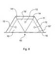
- FIG 7shows an embodiment not in accodance with the present invention of a vertically-stacked array of multi-segmented compound DRA elements 10 each being disposed on a grounded substrate 11 and having a plurality of feeds 12 for transferring energy into and from the DRAs 10.
- each multi-segmented compound DRA 10comprises three generally trapezoidal dielectric resonators 13, 13', 13" arranged on the grounded substrate 11 in a generally semi-hexagonal configuration, with adjacent side faces of the dielectric resonators 13, 13', 13" being separated from each other by a conductive wall 14.
- a conductive backplate 15is provided behind each DRA 10 as shown best in Figure 8.
- Each dielectric resonator 13, 13', 13"includes a monopole feed probe 12. and the feed probes 12 may be activated either individually or in combination by way of electronic circuitry (not shown) connected thereto so as to generate at least one incrementally or continuously steerable beam which may be steered through a predetermined angle ⁇ in azimuth.
- a resultant beamcan be generated which may be steered in elevation ⁇ as well as in azimuth ⁇ .
- the DRAs 10are vertically separated by a nominal spacing of ⁇ /2, where X is the wavelength of the generated beam.
- no weighting or window functionhas been applied, and therefore sidelobe levels are expected to be high. Sidelobes may be improved by increasing the number of DRAs 10 in the array and also by applying a weighting/window function.
- the return loss for each DRA 10 in the present exampleis better than -20dB.
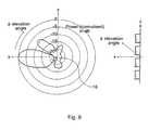
- FIG 9shows the elevation pattern for the array of Figures 7 and 8 with only the central dielectric resonator 13' of each DRA 10 being activated.
- the vertical beamwidthis determined by the 4-element array factor and is around 25° at the -3dB level.
- the backlobe 16is determined to some extent by the size of the backplate 15, and in the present example is around -27dB.
- the length of the conductive walls 14 separating the dielectric resonators 13, 13', 13"can help to determine the azimuth pattern beamwidth. Short walls 14 which do not project significantly beyond the dielectric resonators 13, 13', 13" of the DRA 10 tend to give element beamwidths of around 90°. Longer walls 14 which project further beyond the dielectric resonators 13, 13', 13" can bring this beamwidth down to 40°.
- the array factor beamwidthsare almost identical to the element beamwidths, as expected.
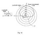
- Figure 10shows the measured azimuth pattern for the array of Figures 7 and 8 with the central dielectric resonator 13' of each DRA 10 being activated.
- DRAs 10 with short walls 14 projecting only just beyond the dielectric resonators 13, 13', 13"were used, and the beamwidth is therefore around 90°.
- the backlobe 17is of the same order as before, that is, around -25dB
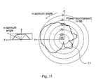
- Figure 11shows the measured azimuth pattern for the array of Figures 7 and 8 with the left-hand dielectric resonators 13 of each DRA 10 being activated. It can be seen that the array factor has been steered by around 75°, and that the backlobe 17 is worse than in Figure 10, being around -13dB.
- the array of Figures 7 and 8may be used as a base station antenna for a GSM mobile communications network, with beamsteering in both azimuth and elevation.
- the elevation patternis controlled by the array factor of the array, and the azimuth pattern by feeding the dielectric resonators 13, 13', 13'' in each DRA 10 in various combinations or individually and also by selecting appropriate lengths for the conducting walls 14.
- Such a base station antennamay be engineered to specifications for a conventional second generation GSM system.
- the antennamay be roughly 10cm wide, 80cm high and 5cm deep, and can be operated so as to generate three independent azimuth beams (which could be combined and steered, or used for direction finding), each one of which may have a 10-15° elevation pattern.
- Each beammay be used on a separate frequency within a 160MHz band.
- appropriate ceramicsas a material for the dielectric resonators 13, 13', 13"
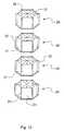
- an array of four DRAs 20each composed of six trapezoidal dielectric resonators 21 arranged in a hexagonal configuration and separated by conductive walls 22 may be used, in an embodiment not in accordance with the present invention as shown in Figure 12.
Landscapes
- Variable-Direction Aerials And Aerial Arrays (AREA)
- Waveguide Aerials (AREA)
- Aerials With Secondary Devices (AREA)
Abstract
Description
| Pattern | Expected | Measured |
| S12 transmission loss of broadside pattern | -52.1dB | -52.1dB |
| S12 transmission loss of 45° pattern, single probe | -54.8dB | -54.9dB |
| S12 transmission loss of 45° pattern, two probes | -53.8dB | -53.9dB |
| Pattern | Expected | Measured |
| Normalised broadside gain (reference) | 0.0dB | 0.0dB |
| Array steered to 45° (0.2 dB cable loss subtracted) | -2.5dB | -2.6dB |
| Array & elements to 45° (1.0dB splitter loss subtracted) | -0.0dB | -0.6dB |
Claims (54)
- An array of dielectric resonator antenna elements (1,10), each element (1,10)having a longitudinal axis and being composed of at least one dielectric resonator(1,13) and a plurality of feeds (2,12) for transferring energy into and from theelements (1,10), wherein the feeds (2,12) of each element (1,10) are activatable eitherindividually or in combination so as to produce at least one incrementally orcontinuously steerable element beam which may be steered in azimuth through apredetermined angle about the longitudinal axis of the element (1,10),the elements (1,10) being disposed side-by-side such that their respectivelongitudinal axes are also disposed side-by-side, wherein during operation of thearray, the feeds (2,12) of the elements (1,10) are activated such that the elementbeams from the different elements (1,10) are steered in synchrony with each other,and the element beams, when combined, interacting so as to form at least onearray beam which is steered in synchrony with the element beams.
- An array as claimed in claim 1, further provided with electronic circuitryadapted to activate the feeds (2,12) either individually or in combination so as toproduce at least one incrementally or continuously steerable element beam whichmay be steered through a predetermined angle.
- An array as claimed in claim 1 or 2, wherein each dielectric resonator (1,13)is associated with a grounded substrate (3,11).
- An array as claimed in claim 1, 2 or 3, wherein the elements (1,10) aredisposed in a substantially linear formation.
- An array as claimed in claim 4, wherein the linear formation is conformal to acurved or distorted surface.
- An array as claimed in claim 1, 2 or 3, wherein the elements (1,10) aredisposed in a ring-like formation.
- An array as claimed in claim 6, wherein the elements (1,10) are disposed in asubstantially circular formation.
- An array as claimed in claim 1, 2 or 3, wherein the elements (1,10) aredisposed in at least two dimensions across a surface.
- An array as claimed in claim 8, wherein the elements (1,10) are arranged inthe form of a lattice.
- An array as claimed in claim 8 or 9, wherein the surface is conformal to acurved or distorted surface.
- An array as claimed in claim 1, 2 or 3, wherein the elements (1,10) arearranged as a three-dimensional volumetric array.
- An array as claimed in claim 11, wherein the volumetric array has an outerenvelope substantially in the form of a regular solid selected from the groupcomprising sphere, tetrahedron, cube, octahedron, dodecahedron and icosahedron.
- An array as claimed in claim 11, wherein the volumetric array has an outerenvelope substantially in the form of a polyhedral solid.
- An array as claimed in claim 11, wherein the volumetric array has an outerenvelope in the form of an irregular solid.
- An array as claimed in any one of claims 11 to 14, wherein the volumetricarray is formed as a combination of linear and/or surface arrays disposed one abovethe other.
- An array as claimed in any preceding claim, wherein the elements (1,10) areregularly spaced from each other.
- An array as claimed in any one of claims 1 to 15, wherein the elements (1,10)are irregularly spaced from each other.
- An array as claimed in any preceding claim, further including a dielectric lenswhich serves to control at least one beam.
- An array as claimed in any preceding claim, further provided with electroniccircuitry adapted to activate each of the elements (1,10) with a pre-determined phaseshift or time delay so as to generate an array beam pattern which may be steeredthrough a predetermined angle.
- An array as claimed in any preceding claim, further provided with electroniccircuitry to combine the feeds (2,12) of at least some of the elements (1,10) such thata generated element beam pattern is steerable in angle in synchronism with agenerated array beam pattern.
- An array as claimed in any preceding claim, further provided with electroniccircuitry to provide at least two feeds (2,12) to each individual element (1,10) suchthat, when the array is used to form at least two array beams simultaneously so as toform an antenna beam pattern having at least two main lobes, the elements (1,10) areactivatable so as to form at least two element beams simultaneously which aresteerable in angle in synchronism with the antenna beam pattern.
- An array as claimed in claim 5 or 10 or any claim depending therefrom,further provided with electronic circuitry to activate the feeds (2,12) eitherindividually or in combination such that the elements (1,10) generate element beamswhich all point in the same direction regardless of the shape of the curved ordistorted surface.
- An array as claimed in any preceding claim, wherein the feeds (2,12) areadapted to provide predetermined time delays in the feed to each element (1,10).
- An array as claimed in claim 23, wherein the feeds (2,12) are connected toelectrical cables, fibre optic cables, printed circuit tracks or any other transmissionlines, each of which having an effective length which may be varied so as to providedifferent time delays in the feeds to the elements (1,10).
- An array as claimed in claim 24, wherein the effective lengths of thetransmission lines are varied by electronically switching in or out additional lengthsof transmission line.
- An array as claimed in claim 24, wherein the effective lengths of thetransmission lines are varied by electrically switching in or out additional lengths oftransmission line.
- An array as claimed in claim 24, wherein the effective lengths of thetransmission lines are varied by mechanically switching in or out additional lengthsof transmission line.
- An array as claimed in any preceding claim, wherein the feeds (2,12) areprovided with means for individually adjusting a phase of an energy signal carriedtherealong to each element (1,10).
- An array as claimed in claim 28, wherein the phase-adjusting means are diodephase shifters, ferrite phase shifters or any other types of phase shifters.
- An array as claimed in any preceding claim, wherein each element (1,10) isconnected to a separate transmitter or receiver module and wherein each transmitteror receiver module is controlled by any means, e.g. a computer, to generatepredetermined phase and/or amplitude modifications to signals fed to or receivedfrom the elements (1,10) so as to enable steering of an array beam pattern.
- An array as claimed in any preceding claim, wherein the steerable elementbeam may be steered through a complete 360 degree circle.
- An array as claimed in any preceding claim, further including electroniccircuitry to combine the feeding mechanisms (2,12) of multiple elements (1,10) so asto form sum and difference patterns to permit radio direction finding capability of upto 360 degrees.
- An array as claimed in any preceding claim, further including electroniccircuitry to combine the feeding mechanisms (2,12) of multiple elements (1,10) toform an amplitude and/or phase comparison radio direction finding capability of upto 360 degrees.
- An array as claimed in any preceding claim, wherein the feeding mechanisms(2,12) take the form of conductive probes (2,12) which are contained within orarranged against the dielectric resonator elements (1,13), or a combination thereof.
- An array as claimed in claim 3 or any one of claims 4 to 33 depending fromclaim 3, wherein the feeding mechanisms (2,12) take the form of apertures providedin the grounded substrate (3,11).
- An array as claimed in claim 35, wherein the apertures are formed asdiscontinuities in the grounded substrate (3,11) underneath the dielectric resonator elements (1,13).
- An array as claimed in claim 36, wherein the apertures are generallyrectangular in shape.
- An array as claimed in any one of claims 35 to 37, wherein a microstriptransmission line is located beneath each aperture to be excited.
- An array as claimed in claim 38, wherein the microstrip transmission line isprinted on a side of the substrate remote from the dielectric resonator elements(1,13).
- An array as claimed in claim 34, wherein a predetermined number of theprobes (2,12) within or against the dielectric resonator elements (1,13), or acombination thereof, are not connected to the electronic circuitry.
- An array as claimed in claim 40, wherein the probes (2,12) are unterminated(open circuit).
- An array as claimed in claim 40, wherein the probes (2,12) are terminated bya load of any impedance, including a short circuit.
- An array as claimed in any preceding claim, wherein the dielectric resonatorelements (1,13) are formed of a dielectric material having a dielectric constant k ≥10.
- An array as claimed in any one of claims 1 to 42, wherein the dielectricresonator elements (1,13) are formed of a dielectric material having a dielectricconstant k ≥ 50.
- An array as claimed in any one of claims 1 to 42, wherein the dielectricresonator elements (1,13) are formed of a dielectric material having a dielectricconstant k ≥ 100.
- An array as claimed in any preceding claim, wherein the dielectric resonatorelements (1,13) are formed from a liquid or gel material.
- An array as claimed in any one of claims I to 45, wherein the dielectricresonator elements (1,13) are formed from a solid material.
- An array as claimed in any one of claims 1 to 45, wherein the dielectricresonator elements (1,13) are formed from a gaseous material.
- An array as claimed in any preceding claim, wherein a single transmitter orreceiver is connected to a plurality of elements (1,10).
- An array as claimed in any one of claims 1 to 48, wherein a plurality oftransmitters or receivers are individually connected to a corresponding plurality ofelements (1,10).
- An array as claimed in any one of claims 1 to 48, wherein a single transmitteror receiver is connected to a plurality of non-adjacent elements (1,10).
- An array as claimed in any preceding claim, wherein each element (10) is acompound dielectric resonator antenna comprising a plurality of individual dielectricresonator antennas each including a dielectric resonator (13,13',13") having sidefaces, and a feeding mechanism (12) for transferring energy into and from thedielectric resonator (13,13',13"), wherein the dielectric resonators (13,13',13") arearranged such that at least one side face of each dielectric resonator (13,13',13") isadjacent to at least one side face of a neighbouring dielectric resonator (13,13',13").
- An array as claimed in claim 52, wherein a gap is provided between at leasttwo of the adjacent side faces.
- An antenna as claimed in claim 52 or 53, wherein the adjacent side faces of atleast one pair (13,13'; 13',13") of neighbouring dielectric resonators (13,13',13")are separated by an electrically conductive wall (14) which contacts both side faces.
Applications Claiming Priority (5)
| Application Number | Priority Date | Filing Date | Title |
|---|---|---|---|
| GB0005766 | 2000-03-11 | ||
| GB0005766AGB2360133B (en) | 2000-03-11 | 2000-03-11 | Multi-segmented dielectric resonator antenna |
| GB0007366AGB2360134B (en) | 2000-03-11 | 2000-03-27 | Dielectric resonator antenna array with steerable elements |
| GB0007366 | 2000-03-27 | ||
| PCT/GB2001/000997WO2001069722A1 (en) | 2000-03-11 | 2001-03-08 | Dielectric resonator antenna array with steerable elements |
Publications (2)
| Publication Number | Publication Date |
|---|---|
| EP1266428A1 EP1266428A1 (en) | 2002-12-18 |
| EP1266428B1true EP1266428B1 (en) | 2004-10-13 |
Family
ID=26243836
Family Applications (1)
| Application Number | Title | Priority Date | Filing Date |
|---|---|---|---|
| EP01915468AExpired - LifetimeEP1266428B1 (en) | 2000-03-11 | 2001-03-08 | Dielectric resonator antenna array with steerable elements |
Country Status (9)
| Country | Link |
|---|---|
| US (1) | US6768454B2 (en) |
| EP (1) | EP1266428B1 (en) |
| JP (1) | JP2004507906A (en) |
| CN (1) | CN1451189A (en) |
| AT (1) | ATE279794T1 (en) |
| AU (1) | AU4256001A (en) |
| CA (1) | CA2402556A1 (en) |
| DE (1) | DE60106405T2 (en) |
| WO (1) | WO2001069722A1 (en) |
Cited By (2)
| Publication number | Priority date | Publication date | Assignee | Title |
|---|---|---|---|---|
| DE102014106060A1 (en)* | 2014-04-30 | 2015-11-19 | Karlsruher Institut für Technologie | antenna array |
| US20170125901A1 (en)* | 2015-11-03 | 2017-05-04 | King Fahd University Of Petroleum And Minerals | Dielectric resonator antenna array system |
Families Citing this family (298)
| Publication number | Priority date | Publication date | Assignee | Title |
|---|---|---|---|---|
| GB0126256D0 (en)* | 2001-11-01 | 2002-01-02 | Antenova Ltd | Adaptive radio antennas |
| GB0211076D0 (en)* | 2002-05-15 | 2002-06-26 | Antenova Ltd | Radio frequency switch for multi-sectored antennas |
| AU2003244740A1 (en)* | 2002-05-22 | 2003-12-02 | Antenova Limited | Array of dielectric resonator antennas |
| US7072718B2 (en)* | 2002-12-03 | 2006-07-04 | Cardiac Pacemakers, Inc. | Antenna systems for implantable medical device telemetry |
| US7197337B2 (en)* | 2003-05-16 | 2007-03-27 | Interdigital Technology Corporation | Coordination of beam forming in wireless communication systems |
| US7373176B2 (en)* | 2003-05-16 | 2008-05-13 | Interdigital Technology Corporation | Coordination of beam forming in wireless communication systems |
| EP1627538A4 (en)* | 2003-05-16 | 2006-12-06 | Interdigital Tech Corp | Coordination of backhaul beam forming in wireless communication systems |
| WO2005114789A2 (en)* | 2004-04-12 | 2005-12-01 | Airgain, Inc. | Switched multi-beam antenna |
| US7071879B2 (en)* | 2004-06-01 | 2006-07-04 | Ems Technologies Canada, Ltd. | Dielectric-resonator array antenna system |
| US8467827B2 (en) | 2005-03-31 | 2013-06-18 | Black Sand Technologies, Inc. | Techniques for partitioning radios in wireless communication systems |
| US7912499B2 (en) | 2005-03-31 | 2011-03-22 | Black Sand Technologies, Inc. | Techniques for partitioning radios in wireless communication systems |
| JP4974168B2 (en)* | 2007-10-02 | 2012-07-11 | 古河電気工業株式会社 | Radar system antenna |
| US7999749B2 (en)* | 2008-10-23 | 2011-08-16 | Sony Ericsson Mobile Communications Ab | Antenna assembly |
| US8149181B2 (en)* | 2009-09-02 | 2012-04-03 | National Tsing Hua University | Dielectric resonator for negative refractivity medium |
| US20120052821A1 (en)* | 2010-08-25 | 2012-03-01 | Dongxun Jia | Perturbation antenna system and apparatus for wireless terminals |
| CN102694604B (en)* | 2012-05-30 | 2015-09-30 | 西安电子科技大学 | For regular dodecahedron omnidirectional optical smart antenna and the communication means of FSO system |
| US9215622B1 (en)* | 2012-07-30 | 2015-12-15 | GoNet Systems Ltd. | Method and systems for associating wireless transmission with directions-of-arrival thereof |
| US9113347B2 (en) | 2012-12-05 | 2015-08-18 | At&T Intellectual Property I, Lp | Backhaul link for distributed antenna system |
| US20220013906A1 (en)* | 2012-12-19 | 2022-01-13 | Go Net Systems Ltd | Methods and systems for using a beam-forming network in conjunction with maximal-ratio-combining techniques |
| US9525524B2 (en) | 2013-05-31 | 2016-12-20 | At&T Intellectual Property I, L.P. | Remote distributed antenna system |
| US9999038B2 (en) | 2013-05-31 | 2018-06-12 | At&T Intellectual Property I, L.P. | Remote distributed antenna system |
| US8897697B1 (en) | 2013-11-06 | 2014-11-25 | At&T Intellectual Property I, Lp | Millimeter-wave surface-wave communications |
| CN104103900B (en)* | 2014-07-10 | 2016-08-17 | 电子科技大学 | A kind of wideband dual polarized omnidirectional antenna of low section |
| US9692101B2 (en) | 2014-08-26 | 2017-06-27 | At&T Intellectual Property I, L.P. | Guided wave couplers for coupling electromagnetic waves between a waveguide surface and a surface of a wire |
| US9768833B2 (en) | 2014-09-15 | 2017-09-19 | At&T Intellectual Property I, L.P. | Method and apparatus for sensing a condition in a transmission medium of electromagnetic waves |
| US10063280B2 (en) | 2014-09-17 | 2018-08-28 | At&T Intellectual Property I, L.P. | Monitoring and mitigating conditions in a communication network |
| US9628854B2 (en) | 2014-09-29 | 2017-04-18 | At&T Intellectual Property I, L.P. | Method and apparatus for distributing content in a communication network |
| US9615269B2 (en) | 2014-10-02 | 2017-04-04 | At&T Intellectual Property I, L.P. | Method and apparatus that provides fault tolerance in a communication network |
| US9685992B2 (en) | 2014-10-03 | 2017-06-20 | At&T Intellectual Property I, L.P. | Circuit panel network and methods thereof |
| US9503189B2 (en) | 2014-10-10 | 2016-11-22 | At&T Intellectual Property I, L.P. | Method and apparatus for arranging communication sessions in a communication system |
| US9973299B2 (en) | 2014-10-14 | 2018-05-15 | At&T Intellectual Property I, L.P. | Method and apparatus for adjusting a mode of communication in a communication network |
| US9985354B2 (en)* | 2014-10-15 | 2018-05-29 | Rogers Corporation | Array apparatus comprising a dielectric resonator array disposed on a ground layer and individually fed by corresponding signal lines, thereby providing a corresponding magnetic dipole vector |
| US9653770B2 (en) | 2014-10-21 | 2017-05-16 | At&T Intellectual Property I, L.P. | Guided wave coupler, coupling module and methods for use therewith |
| US9780834B2 (en) | 2014-10-21 | 2017-10-03 | At&T Intellectual Property I, L.P. | Method and apparatus for transmitting electromagnetic waves |
| US9577306B2 (en) | 2014-10-21 | 2017-02-21 | At&T Intellectual Property I, L.P. | Guided-wave transmission device and methods for use therewith |
| US9564947B2 (en) | 2014-10-21 | 2017-02-07 | At&T Intellectual Property I, L.P. | Guided-wave transmission device with diversity and methods for use therewith |
| US9627768B2 (en) | 2014-10-21 | 2017-04-18 | At&T Intellectual Property I, L.P. | Guided-wave transmission device with non-fundamental mode propagation and methods for use therewith |
| US9520945B2 (en) | 2014-10-21 | 2016-12-13 | At&T Intellectual Property I, L.P. | Apparatus for providing communication services and methods thereof |
| US9769020B2 (en) | 2014-10-21 | 2017-09-19 | At&T Intellectual Property I, L.P. | Method and apparatus for responding to events affecting communications in a communication network |
| US9312919B1 (en) | 2014-10-21 | 2016-04-12 | At&T Intellectual Property I, Lp | Transmission device with impairment compensation and methods for use therewith |
| US9923591B2 (en)* | 2014-11-12 | 2018-03-20 | Sony Corporation | Array antennas including non-uniform antenna elements |
| US10340573B2 (en) | 2016-10-26 | 2019-07-02 | At&T Intellectual Property I, L.P. | Launcher with cylindrical coupling device and methods for use therewith |
| US9997819B2 (en) | 2015-06-09 | 2018-06-12 | At&T Intellectual Property I, L.P. | Transmission medium and method for facilitating propagation of electromagnetic waves via a core |
| US10243784B2 (en) | 2014-11-20 | 2019-03-26 | At&T Intellectual Property I, L.P. | System for generating topology information and methods thereof |
| US9544006B2 (en) | 2014-11-20 | 2017-01-10 | At&T Intellectual Property I, L.P. | Transmission device with mode division multiplexing and methods for use therewith |
| US9742462B2 (en) | 2014-12-04 | 2017-08-22 | At&T Intellectual Property I, L.P. | Transmission medium and communication interfaces and methods for use therewith |
| US9461706B1 (en) | 2015-07-31 | 2016-10-04 | At&T Intellectual Property I, Lp | Method and apparatus for exchanging communication signals |
| US9954287B2 (en) | 2014-11-20 | 2018-04-24 | At&T Intellectual Property I, L.P. | Apparatus for converting wireless signals and electromagnetic waves and methods thereof |
| US9800327B2 (en) | 2014-11-20 | 2017-10-24 | At&T Intellectual Property I, L.P. | Apparatus for controlling operations of a communication device and methods thereof |
| US10009067B2 (en) | 2014-12-04 | 2018-06-26 | At&T Intellectual Property I, L.P. | Method and apparatus for configuring a communication interface |
| US10411920B2 (en) | 2014-11-20 | 2019-09-10 | At&T Intellectual Property I, L.P. | Methods and apparatus for inducing electromagnetic waves within pathways of a cable |
| US11025460B2 (en) | 2014-11-20 | 2021-06-01 | At&T Intellectual Property I, L.P. | Methods and apparatus for accessing interstitial areas of a cable |
| WO2016190907A2 (en)* | 2015-01-20 | 2016-12-01 | Ohio University | Single-element patch antenna with pattern control |
| US9876570B2 (en) | 2015-02-20 | 2018-01-23 | At&T Intellectual Property I, Lp | Guided-wave transmission device with non-fundamental mode propagation and methods for use therewith |
| US9749013B2 (en) | 2015-03-17 | 2017-08-29 | At&T Intellectual Property I, L.P. | Method and apparatus for reducing attenuation of electromagnetic waves guided by a transmission medium |
| US10224981B2 (en) | 2015-04-24 | 2019-03-05 | At&T Intellectual Property I, Lp | Passive electrical coupling device and methods for use therewith |
| US9705561B2 (en) | 2015-04-24 | 2017-07-11 | At&T Intellectual Property I, L.P. | Directional coupling device and methods for use therewith |
| US9793954B2 (en) | 2015-04-28 | 2017-10-17 | At&T Intellectual Property I, L.P. | Magnetic coupling device and methods for use therewith |
| US10714803B2 (en) | 2015-05-14 | 2020-07-14 | At&T Intellectual Property I, L.P. | Transmission medium and methods for use therewith |
| US9748626B2 (en) | 2015-05-14 | 2017-08-29 | At&T Intellectual Property I, L.P. | Plurality of cables having different cross-sectional shapes which are bundled together to form a transmission medium |
| US9871282B2 (en) | 2015-05-14 | 2018-01-16 | At&T Intellectual Property I, L.P. | At least one transmission medium having a dielectric surface that is covered at least in part by a second dielectric |
| US9490869B1 (en) | 2015-05-14 | 2016-11-08 | At&T Intellectual Property I, L.P. | Transmission medium having multiple cores and methods for use therewith |
| US10650940B2 (en) | 2015-05-15 | 2020-05-12 | At&T Intellectual Property I, L.P. | Transmission medium having a conductive material and methods for use therewith |
| US9917341B2 (en) | 2015-05-27 | 2018-03-13 | At&T Intellectual Property I, L.P. | Apparatus and method for launching electromagnetic waves and for modifying radial dimensions of the propagating electromagnetic waves |
| US10812174B2 (en) | 2015-06-03 | 2020-10-20 | At&T Intellectual Property I, L.P. | Client node device and methods for use therewith |
| US9866309B2 (en) | 2015-06-03 | 2018-01-09 | At&T Intellectual Property I, Lp | Host node device and methods for use therewith |
| US10756805B2 (en) | 2015-06-03 | 2020-08-25 | At&T Intellectual Property I, L.P. | Client node device with frequency conversion and methods for use therewith |
| US9912381B2 (en) | 2015-06-03 | 2018-03-06 | At&T Intellectual Property I, Lp | Network termination and methods for use therewith |
| US9913139B2 (en) | 2015-06-09 | 2018-03-06 | At&T Intellectual Property I, L.P. | Signal fingerprinting for authentication of communicating devices |
| US9608692B2 (en) | 2015-06-11 | 2017-03-28 | At&T Intellectual Property I, L.P. | Repeater and methods for use therewith |
| US10142086B2 (en) | 2015-06-11 | 2018-11-27 | At&T Intellectual Property I, L.P. | Repeater and methods for use therewith |
| US9820146B2 (en) | 2015-06-12 | 2017-11-14 | At&T Intellectual Property I, L.P. | Method and apparatus for authentication and identity management of communicating devices |
| US9865911B2 (en) | 2015-06-25 | 2018-01-09 | At&T Intellectual Property I, L.P. | Waveguide system for slot radiating first electromagnetic waves that are combined into a non-fundamental wave mode second electromagnetic wave on a transmission medium |
| US9640850B2 (en) | 2015-06-25 | 2017-05-02 | At&T Intellectual Property I, L.P. | Methods and apparatus for inducing a non-fundamental wave mode on a transmission medium |
| US9509415B1 (en) | 2015-06-25 | 2016-11-29 | At&T Intellectual Property I, L.P. | Methods and apparatus for inducing a fundamental wave mode on a transmission medium |
| US9847566B2 (en) | 2015-07-14 | 2017-12-19 | At&T Intellectual Property I, L.P. | Method and apparatus for adjusting a field of a signal to mitigate interference |
| US9882257B2 (en) | 2015-07-14 | 2018-01-30 | At&T Intellectual Property I, L.P. | Method and apparatus for launching a wave mode that mitigates interference |
| US10129057B2 (en) | 2015-07-14 | 2018-11-13 | At&T Intellectual Property I, L.P. | Apparatus and methods for inducing electromagnetic waves on a cable |
| US9628116B2 (en) | 2015-07-14 | 2017-04-18 | At&T Intellectual Property I, L.P. | Apparatus and methods for transmitting wireless signals |
| US10341142B2 (en) | 2015-07-14 | 2019-07-02 | At&T Intellectual Property I, L.P. | Apparatus and methods for generating non-interfering electromagnetic waves on an uninsulated conductor |
| US9722318B2 (en) | 2015-07-14 | 2017-08-01 | At&T Intellectual Property I, L.P. | Method and apparatus for coupling an antenna to a device |
| US10742243B2 (en) | 2015-07-14 | 2020-08-11 | At&T Intellectual Property I, L.P. | Method and apparatus for coupling an antenna to a device |
| US10170840B2 (en) | 2015-07-14 | 2019-01-01 | At&T Intellectual Property I, L.P. | Apparatus and methods for sending or receiving electromagnetic signals |
| US10148016B2 (en) | 2015-07-14 | 2018-12-04 | At&T Intellectual Property I, L.P. | Apparatus and methods for communicating utilizing an antenna array |
| US10033107B2 (en) | 2015-07-14 | 2018-07-24 | At&T Intellectual Property I, L.P. | Method and apparatus for coupling an antenna to a device |
| US10044409B2 (en) | 2015-07-14 | 2018-08-07 | At&T Intellectual Property I, L.P. | Transmission medium and methods for use therewith |
| US10205655B2 (en) | 2015-07-14 | 2019-02-12 | At&T Intellectual Property I, L.P. | Apparatus and methods for communicating utilizing an antenna array and multiple communication paths |
| US9853342B2 (en) | 2015-07-14 | 2017-12-26 | At&T Intellectual Property I, L.P. | Dielectric transmission medium connector and methods for use therewith |
| US9608740B2 (en) | 2015-07-15 | 2017-03-28 | At&T Intellectual Property I, L.P. | Method and apparatus for launching a wave mode that mitigates interference |
| US10090606B2 (en) | 2015-07-15 | 2018-10-02 | At&T Intellectual Property I, L.P. | Antenna system with dielectric array and methods for use therewith |
| US9793951B2 (en) | 2015-07-15 | 2017-10-17 | At&T Intellectual Property I, L.P. | Method and apparatus for launching a wave mode that mitigates interference |
| US9948333B2 (en) | 2015-07-23 | 2018-04-17 | At&T Intellectual Property I, L.P. | Method and apparatus for wireless communications to mitigate interference |
| US9749053B2 (en) | 2015-07-23 | 2017-08-29 | At&T Intellectual Property I, L.P. | Node device, repeater and methods for use therewith |
| US9871283B2 (en) | 2015-07-23 | 2018-01-16 | At&T Intellectual Property I, Lp | Transmission medium having a dielectric core comprised of plural members connected by a ball and socket configuration |
| US9912027B2 (en) | 2015-07-23 | 2018-03-06 | At&T Intellectual Property I, L.P. | Method and apparatus for exchanging communication signals |
| US10020587B2 (en) | 2015-07-31 | 2018-07-10 | At&T Intellectual Property I, L.P. | Radial antenna and methods for use therewith |
| US9735833B2 (en) | 2015-07-31 | 2017-08-15 | At&T Intellectual Property I, L.P. | Method and apparatus for communications management in a neighborhood network |
| US9967173B2 (en) | 2015-07-31 | 2018-05-08 | At&T Intellectual Property I, L.P. | Method and apparatus for authentication and identity management of communicating devices |
| US9904535B2 (en) | 2015-09-14 | 2018-02-27 | At&T Intellectual Property I, L.P. | Method and apparatus for distributing software |
| US10009063B2 (en) | 2015-09-16 | 2018-06-26 | At&T Intellectual Property I, L.P. | Method and apparatus for use with a radio distributed antenna system having an out-of-band reference signal |
| US10009901B2 (en) | 2015-09-16 | 2018-06-26 | At&T Intellectual Property I, L.P. | Method, apparatus, and computer-readable storage medium for managing utilization of wireless resources between base stations |
| US9769128B2 (en) | 2015-09-28 | 2017-09-19 | At&T Intellectual Property I, L.P. | Method and apparatus for encryption of communications over a network |
| US9729197B2 (en) | 2015-10-01 | 2017-08-08 | At&T Intellectual Property I, L.P. | Method and apparatus for communicating network management traffic over a network |
| US9876264B2 (en) | 2015-10-02 | 2018-01-23 | At&T Intellectual Property I, Lp | Communication system, guided wave switch and methods for use therewith |
| US10051483B2 (en)* | 2015-10-16 | 2018-08-14 | At&T Intellectual Property I, L.P. | Method and apparatus for directing wireless signals |
| US10355367B2 (en) | 2015-10-16 | 2019-07-16 | At&T Intellectual Property I, L.P. | Antenna structure for exchanging wireless signals |
| US10601137B2 (en) | 2015-10-28 | 2020-03-24 | Rogers Corporation | Broadband multiple layer dielectric resonator antenna and method of making the same |
| US10374315B2 (en) | 2015-10-28 | 2019-08-06 | Rogers Corporation | Broadband multiple layer dielectric resonator antenna and method of making the same |
| US10355361B2 (en) | 2015-10-28 | 2019-07-16 | Rogers Corporation | Dielectric resonator antenna and method of making the same |
| US11367959B2 (en) | 2015-10-28 | 2022-06-21 | Rogers Corporation | Broadband multiple layer dielectric resonator antenna and method of making the same |
| US10476164B2 (en) | 2015-10-28 | 2019-11-12 | Rogers Corporation | Broadband multiple layer dielectric resonator antenna and method of making the same |
| KR101788443B1 (en)* | 2016-02-18 | 2017-10-19 | 한국과학기술원 | Pattern/polarization antenna apparatus |
| CN106291457B (en)* | 2016-03-23 | 2019-02-19 | 吉林省亿丰无线电技术股份有限公司 | A kind of 3 D stereo radio-signal direction finding localization method |
| US10763583B2 (en)* | 2016-05-10 | 2020-09-01 | Kymeta Corporation | Method to assemble aperture segments of a cylindrical feed antenna |
| US9912419B1 (en) | 2016-08-24 | 2018-03-06 | At&T Intellectual Property I, L.P. | Method and apparatus for managing a fault in a distributed antenna system |
| US9860075B1 (en) | 2016-08-26 | 2018-01-02 | At&T Intellectual Property I, L.P. | Method and communication node for broadband distribution |
| US10135147B2 (en) | 2016-10-18 | 2018-11-20 | At&T Intellectual Property I, L.P. | Apparatus and methods for launching guided waves via an antenna |
| US10135146B2 (en) | 2016-10-18 | 2018-11-20 | At&T Intellectual Property I, L.P. | Apparatus and methods for launching guided waves via circuits |
| US9991580B2 (en) | 2016-10-21 | 2018-06-05 | At&T Intellectual Property I, L.P. | Launcher and coupling system for guided wave mode cancellation |
| US10374316B2 (en) | 2016-10-21 | 2019-08-06 | At&T Intellectual Property I, L.P. | System and dielectric antenna with non-uniform dielectric |
| US10811767B2 (en) | 2016-10-21 | 2020-10-20 | At&T Intellectual Property I, L.P. | System and dielectric antenna with convex dielectric radome |
| US9876605B1 (en) | 2016-10-21 | 2018-01-23 | At&T Intellectual Property I, L.P. | Launcher and coupling system to support desired guided wave mode |
| US10312567B2 (en) | 2016-10-26 | 2019-06-04 | At&T Intellectual Property I, L.P. | Launcher with planar strip antenna and methods for use therewith |
| US10224634B2 (en) | 2016-11-03 | 2019-03-05 | At&T Intellectual Property I, L.P. | Methods and apparatus for adjusting an operational characteristic of an antenna |
| US10498044B2 (en) | 2016-11-03 | 2019-12-03 | At&T Intellectual Property I, L.P. | Apparatus for configuring a surface of an antenna |
| US10225025B2 (en) | 2016-11-03 | 2019-03-05 | At&T Intellectual Property I, L.P. | Method and apparatus for detecting a fault in a communication system |
| US10291334B2 (en) | 2016-11-03 | 2019-05-14 | At&T Intellectual Property I, L.P. | System for detecting a fault in a communication system |
| DE102016122189A1 (en) | 2016-11-18 | 2018-05-24 | Valeo Schalter Und Sensoren Gmbh | Radar sensor for a motor vehicle with an integrated into a radome antenna element, driver assistance system and motor vehicle |
| US10178445B2 (en) | 2016-11-23 | 2019-01-08 | At&T Intellectual Property I, L.P. | Methods, devices, and systems for load balancing between a plurality of waveguides |
| US10090594B2 (en) | 2016-11-23 | 2018-10-02 | At&T Intellectual Property I, L.P. | Antenna system having structural configurations for assembly |
| US10535928B2 (en) | 2016-11-23 | 2020-01-14 | At&T Intellectual Property I, L.P. | Antenna system and methods for use therewith |
| US10340601B2 (en) | 2016-11-23 | 2019-07-02 | At&T Intellectual Property I, L.P. | Multi-antenna system and methods for use therewith |
| US10340603B2 (en) | 2016-11-23 | 2019-07-02 | At&T Intellectual Property I, L.P. | Antenna system having shielded structural configurations for assembly |
| US10361489B2 (en) | 2016-12-01 | 2019-07-23 | At&T Intellectual Property I, L.P. | Dielectric dish antenna system and methods for use therewith |
| US10305190B2 (en) | 2016-12-01 | 2019-05-28 | At&T Intellectual Property I, L.P. | Reflecting dielectric antenna system and methods for use therewith |
| US9927517B1 (en) | 2016-12-06 | 2018-03-27 | At&T Intellectual Property I, L.P. | Apparatus and methods for sensing rainfall |
| US10439675B2 (en) | 2016-12-06 | 2019-10-08 | At&T Intellectual Property I, L.P. | Method and apparatus for repeating guided wave communication signals |
| US10020844B2 (en) | 2016-12-06 | 2018-07-10 | T&T Intellectual Property I, L.P. | Method and apparatus for broadcast communication via guided waves |
| US10382976B2 (en) | 2016-12-06 | 2019-08-13 | At&T Intellectual Property I, L.P. | Method and apparatus for managing wireless communications based on communication paths and network device positions |
| US10727599B2 (en) | 2016-12-06 | 2020-07-28 | At&T Intellectual Property I, L.P. | Launcher with slot antenna and methods for use therewith |
| US10819035B2 (en) | 2016-12-06 | 2020-10-27 | At&T Intellectual Property I, L.P. | Launcher with helical antenna and methods for use therewith |
| US10326494B2 (en) | 2016-12-06 | 2019-06-18 | At&T Intellectual Property I, L.P. | Apparatus for measurement de-embedding and methods for use therewith |
| US10637149B2 (en) | 2016-12-06 | 2020-04-28 | At&T Intellectual Property I, L.P. | Injection molded dielectric antenna and methods for use therewith |
| US10755542B2 (en) | 2016-12-06 | 2020-08-25 | At&T Intellectual Property I, L.P. | Method and apparatus for surveillance via guided wave communication |
| US10694379B2 (en) | 2016-12-06 | 2020-06-23 | At&T Intellectual Property I, L.P. | Waveguide system with device-based authentication and methods for use therewith |
| US10205212B2 (en) | 2016-12-06 | 2019-02-12 | At&T Intellectual Property I, L.P. | Methods and apparatus for adjusting a phase of electromagnetic waves |
| US10135145B2 (en) | 2016-12-06 | 2018-11-20 | At&T Intellectual Property I, L.P. | Apparatus and methods for generating an electromagnetic wave along a transmission medium |
| US10547348B2 (en) | 2016-12-07 | 2020-01-28 | At&T Intellectual Property I, L.P. | Method and apparatus for switching transmission mediums in a communication system |
| US10446936B2 (en) | 2016-12-07 | 2019-10-15 | At&T Intellectual Property I, L.P. | Multi-feed dielectric antenna system and methods for use therewith |
| US10168695B2 (en) | 2016-12-07 | 2019-01-01 | At&T Intellectual Property I, L.P. | Method and apparatus for controlling an unmanned aircraft |
| US10359749B2 (en) | 2016-12-07 | 2019-07-23 | At&T Intellectual Property I, L.P. | Method and apparatus for utilities management via guided wave communication |
| US10389029B2 (en) | 2016-12-07 | 2019-08-20 | At&T Intellectual Property I, L.P. | Multi-feed dielectric antenna system with core selection and methods for use therewith |
| US10243270B2 (en) | 2016-12-07 | 2019-03-26 | At&T Intellectual Property I, L.P. | Beam adaptive multi-feed dielectric antenna system and methods for use therewith |
| US9893795B1 (en) | 2016-12-07 | 2018-02-13 | At&T Intellectual Property I, Lp | Method and repeater for broadband distribution |
| US10139820B2 (en) | 2016-12-07 | 2018-11-27 | At&T Intellectual Property I, L.P. | Method and apparatus for deploying equipment of a communication system |
| US10027397B2 (en) | 2016-12-07 | 2018-07-17 | At&T Intellectual Property I, L.P. | Distributed antenna system and methods for use therewith |
| US10264467B2 (en) | 2016-12-08 | 2019-04-16 | At&T Intellectual Property I, L.P. | Method and apparatus for collecting data associated with wireless communications |
| US10326689B2 (en) | 2016-12-08 | 2019-06-18 | At&T Intellectual Property I, L.P. | Method and system for providing alternative communication paths |
| US10916969B2 (en) | 2016-12-08 | 2021-02-09 | At&T Intellectual Property I, L.P. | Method and apparatus for providing power using an inductive coupling |
| US10601494B2 (en) | 2016-12-08 | 2020-03-24 | At&T Intellectual Property I, L.P. | Dual-band communication device and method for use therewith |
| US10136255B2 (en) | 2016-12-08 | 2018-11-20 | At&T Intellectual Property I, L.P. | Method and apparatus for proximity sensing on a communication device |
| US10777873B2 (en) | 2016-12-08 | 2020-09-15 | At&T Intellectual Property I, L.P. | Method and apparatus for mounting network devices |
| US10530505B2 (en) | 2016-12-08 | 2020-01-07 | At&T Intellectual Property I, L.P. | Apparatus and methods for launching electromagnetic waves along a transmission medium |
| US10938108B2 (en) | 2016-12-08 | 2021-03-02 | At&T Intellectual Property I, L.P. | Frequency selective multi-feed dielectric antenna system and methods for use therewith |
| US9998870B1 (en) | 2016-12-08 | 2018-06-12 | At&T Intellectual Property I, L.P. | Method and apparatus for proximity sensing |
| US10103422B2 (en) | 2016-12-08 | 2018-10-16 | At&T Intellectual Property I, L.P. | Method and apparatus for mounting network devices |
| US10411356B2 (en) | 2016-12-08 | 2019-09-10 | At&T Intellectual Property I, L.P. | Apparatus and methods for selectively targeting communication devices with an antenna array |
| US9911020B1 (en) | 2016-12-08 | 2018-03-06 | At&T Intellectual Property I, L.P. | Method and apparatus for tracking via a radio frequency identification device |
| US10389037B2 (en) | 2016-12-08 | 2019-08-20 | At&T Intellectual Property I, L.P. | Apparatus and methods for selecting sections of an antenna array and use therewith |
| US10069535B2 (en) | 2016-12-08 | 2018-09-04 | At&T Intellectual Property I, L.P. | Apparatus and methods for launching electromagnetic waves having a certain electric field structure |
| US9838896B1 (en) | 2016-12-09 | 2017-12-05 | At&T Intellectual Property I, L.P. | Method and apparatus for assessing network coverage |
| US10264586B2 (en) | 2016-12-09 | 2019-04-16 | At&T Mobility Ii Llc | Cloud-based packet controller and methods for use therewith |
| US10340983B2 (en) | 2016-12-09 | 2019-07-02 | At&T Intellectual Property I, L.P. | Method and apparatus for surveying remote sites via guided wave communications |
| CN106684533A (en)* | 2016-12-21 | 2017-05-17 | 华南理工大学 | Dielectric radiator unit and antenna device |
| US9973940B1 (en) | 2017-02-27 | 2018-05-15 | At&T Intellectual Property I, L.P. | Apparatus and methods for dynamic impedance matching of a guided wave launcher |
| US10298293B2 (en) | 2017-03-13 | 2019-05-21 | At&T Intellectual Property I, L.P. | Apparatus of communication utilizing wireless network devices |
| US10097241B1 (en) | 2017-04-11 | 2018-10-09 | At&T Intellectual Property I, L.P. | Machine assisted development of deployment site inventory |
| US11876295B2 (en)* | 2017-05-02 | 2024-01-16 | Rogers Corporation | Electromagnetic reflector for use in a dielectric resonator antenna system |
| US11283189B2 (en) | 2017-05-02 | 2022-03-22 | Rogers Corporation | Connected dielectric resonator antenna array and method of making the same |
| EP3620029A1 (en)* | 2017-05-03 | 2020-03-11 | IDAC Holdings, Inc. | Beam recovery mechanism |
| KR102312067B1 (en) | 2017-06-07 | 2021-10-13 | 로저스코포레이션 | Dielectric Resonator Antenna System |
| US10727583B2 (en) | 2017-07-05 | 2020-07-28 | At&T Intellectual Property I, L.P. | Method and apparatus for steering radiation on an outer surface of a structure |
| US10389403B2 (en) | 2017-07-05 | 2019-08-20 | At&T Intellectual Property I, L.P. | Method and apparatus for reducing flow of currents on an outer surface of a structure |
| US10103777B1 (en) | 2017-07-05 | 2018-10-16 | At&T Intellectual Property I, L.P. | Method and apparatus for reducing radiation from an external surface of a waveguide structure |
| US10446899B2 (en) | 2017-09-05 | 2019-10-15 | At&T Intellectual Property I, L.P. | Flared dielectric coupling system and methods for use therewith |
| US10374277B2 (en) | 2017-09-05 | 2019-08-06 | At&T Intellectual Property I, L.P. | Multi-arm dielectric coupling system and methods for use therewith |
| US10714831B2 (en) | 2017-10-19 | 2020-07-14 | At&T Intellectual Property I, L.P. | Dual mode communications device with remote radio head and methods for use therewith |
| US10244408B1 (en) | 2017-10-19 | 2019-03-26 | At&T Intellectual Property I, L.P. | Dual mode communications device with null steering and methods for use therewith |
| US10051488B1 (en) | 2017-10-19 | 2018-08-14 | At&T Intellectual Property I, L.P. | Dual mode communications device with remote device feedback and methods for use therewith |
| US10374278B2 (en) | 2017-09-05 | 2019-08-06 | At&T Intellectual Property I, L.P. | Dielectric coupling system with mode control and methods for use therewith |
| US10230426B1 (en) | 2017-09-06 | 2019-03-12 | At&T Intellectual Property I, L.P. | Antenna structure with circularly polarized antenna beam |
| US10305197B2 (en) | 2017-09-06 | 2019-05-28 | At&T Intellectual Property I, L.P. | Multimode antenna system and methods for use therewith |
| US9998172B1 (en) | 2017-10-04 | 2018-06-12 | At&T Intellectual Property I, L.P. | Apparatus and methods for processing ultra-wideband electromagnetic waves |
| US10764762B2 (en) | 2017-10-04 | 2020-09-01 | At&T Intellectual Property I, L.P. | Apparatus and methods for distributing a communication signal obtained from ultra-wideband electromagnetic waves |
| US10498589B2 (en) | 2017-10-04 | 2019-12-03 | At&T Intellectual Property I, L.P. | Apparatus and methods for mitigating a fault that adversely affects ultra-wideband transmissions |
| US10123217B1 (en) | 2017-10-04 | 2018-11-06 | At&T Intellectual Property I, L.P. | Apparatus and methods for communicating with ultra-wideband electromagnetic waves |
| US10763916B2 (en) | 2017-10-19 | 2020-09-01 | At&T Intellectual Property I, L.P. | Dual mode antenna systems and methods for use therewith |
| US10553960B2 (en) | 2017-10-26 | 2020-02-04 | At&T Intellectual Property I, L.P. | Antenna system with planar antenna and methods for use therewith |
| US10553959B2 (en) | 2017-10-26 | 2020-02-04 | At&T Intellectual Property I, L.P. | Antenna system with planar antenna and directors and methods for use therewith |
| US10554235B2 (en) | 2017-11-06 | 2020-02-04 | At&T Intellectual Property I, L.P. | Multi-input multi-output guided wave system and methods for use therewith |
| US10355745B2 (en) | 2017-11-09 | 2019-07-16 | At&T Intellectual Property I, L.P. | Guided wave communication system with interference mitigation and methods for use therewith |
| US10555318B2 (en) | 2017-11-09 | 2020-02-04 | At&T Intellectual Property I, L.P. | Guided wave communication system with resource allocation and methods for use therewith |
| US10555249B2 (en) | 2017-11-15 | 2020-02-04 | At&T Intellectual Property I, L.P. | Access point and methods for communicating resource blocks with guided electromagnetic waves |
| US10284261B1 (en) | 2017-11-15 | 2019-05-07 | At&T Intellectual Property I, L.P. | Access point and methods for communicating with guided electromagnetic waves |
| US10389419B2 (en) | 2017-12-01 | 2019-08-20 | At&T Intellectual Property I, L.P. | Methods and apparatus for generating and receiving electromagnetic waves |
| US10820329B2 (en) | 2017-12-04 | 2020-10-27 | At&T Intellectual Property I, L.P. | Guided wave communication system with interference mitigation and methods for use therewith |
| US10424845B2 (en) | 2017-12-06 | 2019-09-24 | At&T Intellectual Property I, L.P. | Method and apparatus for communication using variable permittivity polyrod antenna |
| US10680308B2 (en) | 2017-12-07 | 2020-06-09 | At&T Intellectual Property I, L.P. | Methods and apparatus for bidirectional exchange of electromagnetic waves |
| US11018525B2 (en) | 2017-12-07 | 2021-05-25 | At&T Intellectual Property 1, L.P. | Methods and apparatus for increasing a transfer of energy in an inductive power supply |
| US10892544B2 (en) | 2018-01-15 | 2021-01-12 | Rogers Corporation | Dielectric resonator antenna having first and second dielectric portions |
| US10910722B2 (en) | 2018-01-15 | 2021-02-02 | Rogers Corporation | Dielectric resonator antenna having first and second dielectric portions |
| US11616302B2 (en) | 2018-01-15 | 2023-03-28 | Rogers Corporation | Dielectric resonator antenna having first and second dielectric portions |
| US11233337B2 (en) | 2018-03-02 | 2022-01-25 | Samsung Electro-Mechanics Co., Ltd. | Antenna apparatus |
| US10340979B1 (en) | 2018-03-26 | 2019-07-02 | At&T Intellectual Property I, L.P. | Surface wave communication system and methods for use therewith |
| US10326495B1 (en) | 2018-03-26 | 2019-06-18 | At&T Intellectual Property I, L.P. | Coaxial surface wave communication system and methods for use therewith |
| US10686493B2 (en) | 2018-03-26 | 2020-06-16 | At&T Intellectual Property I, L.P. | Switching of data channels provided in electromagnetic waves and methods thereof |
| US10727577B2 (en) | 2018-03-29 | 2020-07-28 | At&T Intellectual Property I, L.P. | Exchange of wireless signals guided by a transmission medium and methods thereof |
| US10547545B2 (en) | 2018-03-30 | 2020-01-28 | At&T Intellectual Property I, L.P. | Method and apparatus for switching of data channels provided in electromagnetic waves |
| US10581275B2 (en) | 2018-03-30 | 2020-03-03 | At&T Intellectual Property I, L.P. | Methods and apparatus for regulating a magnetic flux in an inductive power supply |
| US10419074B1 (en) | 2018-05-16 | 2019-09-17 | At&T Intellectual Property I, L.P. | Method and apparatus for communications using electromagnetic waves and an insulator |
| US11962091B2 (en)* | 2018-06-06 | 2024-04-16 | Ramot At Tel-Aviv University Ltd. | Integrated array antenna |
| US10804962B2 (en) | 2018-07-09 | 2020-10-13 | At&T Intellectual Property I, L.P. | Method and apparatus for communications using electromagnetic waves |
| KR102484484B1 (en)* | 2018-07-11 | 2023-01-04 | 삼성전자주식회사 | Electronic device comprising array antenna |
| US10305192B1 (en) | 2018-08-13 | 2019-05-28 | At&T Intellectual Property I, L.P. | System and method for launching guided electromagnetic waves with impedance matching |
| US11552390B2 (en) | 2018-09-11 | 2023-01-10 | Rogers Corporation | Dielectric resonator antenna system |
| US10405199B1 (en) | 2018-09-12 | 2019-09-03 | At&T Intellectual Property I, L.P. | Apparatus and methods for transmitting or receiving electromagnetic waves |
| US10778286B2 (en) | 2018-09-12 | 2020-09-15 | At&T Intellectual Property I, L.P. | Methods and apparatus for transmitting or receiving electromagnetic waves |
| US10833727B2 (en) | 2018-10-02 | 2020-11-10 | At&T Intellectual Property I, L.P. | Methods and apparatus for launching or receiving electromagnetic waves |
| US10587310B1 (en) | 2018-10-10 | 2020-03-10 | At&T Intellectual Property I, L.P. | Methods and apparatus for selectively controlling energy consumption of a waveguide system |
| US10693667B2 (en) | 2018-10-12 | 2020-06-23 | At&T Intellectual Property I, L.P. | Methods and apparatus for exchanging communication signals via a cable of twisted pair wires |
| US10516197B1 (en) | 2018-10-18 | 2019-12-24 | At&T Intellectual Property I, L.P. | System and method for launching scattering electromagnetic waves |
| US10505584B1 (en) | 2018-11-14 | 2019-12-10 | At&T Intellectual Property I, L.P. | Device with resonant cavity for transmitting or receiving electromagnetic waves |
| US10957977B2 (en) | 2018-11-14 | 2021-03-23 | At&T Intellectual Property I, L.P. | Device with virtual reflector for transmitting or receiving electromagnetic waves |
| US10523269B1 (en) | 2018-11-14 | 2019-12-31 | At&T Intellectual Property I, L.P. | Device with configurable reflector for transmitting or receiving electromagnetic waves |
| US10931012B2 (en) | 2018-11-14 | 2021-02-23 | At&T Intellectual Property I, L.P. | Device with programmable reflector for transmitting or receiving electromagnetic waves |
| US10938104B2 (en) | 2018-11-16 | 2021-03-02 | At&T Intellectual Property I, L.P. | Method and apparatus for mitigating a change in an orientation of an antenna |
| US10965344B2 (en) | 2018-11-29 | 2021-03-30 | At&T Intellectual Property 1, L.P. | Methods and apparatus for exchanging wireless signals utilizing electromagnetic waves having differing characteristics |
| US10623033B1 (en) | 2018-11-29 | 2020-04-14 | At&T Intellectual Property I, L.P. | Methods and apparatus to reduce distortion between electromagnetic wave transmissions |
| US11082091B2 (en) | 2018-11-29 | 2021-08-03 | At&T Intellectual Property I, L.P. | Method and apparatus for communication utilizing electromagnetic waves and a power line |
| US10812139B2 (en) | 2018-11-29 | 2020-10-20 | At&T Intellectual Property I, L.P. | Method and apparatus for communication utilizing electromagnetic waves and a telecommunication line |
| US10727955B2 (en) | 2018-11-29 | 2020-07-28 | At&T Intellectual Property I, L.P. | Method and apparatus for power delivery to waveguide systems |
| US10371889B1 (en) | 2018-11-29 | 2019-08-06 | At&T Intellectual Property I, L.P. | Method and apparatus for providing power to waveguide systems |
| US11031697B2 (en) | 2018-11-29 | 2021-06-08 | Rogers Corporation | Electromagnetic device |
| US10978773B2 (en) | 2018-12-03 | 2021-04-13 | At&T Intellectual Property I, L.P. | Guided wave dielectric coupler having a dielectric cable with an exposed dielectric core position for enabling electromagnetic coupling between the cable and a transmission medium |
| US10819391B2 (en) | 2018-12-03 | 2020-10-27 | At&T Intellectual Property I, L.P. | Guided wave launcher with reflector and methods for use therewith |
| US11283182B2 (en) | 2018-12-03 | 2022-03-22 | At&T Intellectual Property I, L.P. | Guided wave launcher with lens and methods for use therewith |
| US10623056B1 (en) | 2018-12-03 | 2020-04-14 | At&T Intellectual Property I, L.P. | Guided wave splitter and methods for use therewith |
| US10785125B2 (en) | 2018-12-03 | 2020-09-22 | At&T Intellectual Property I, L.P. | Method and procedure for generating reputation scores for IoT devices based on distributed analysis |
| US11171960B2 (en) | 2018-12-03 | 2021-11-09 | At&T Intellectual Property I, L.P. | Network security management based on collection and cataloging of network-accessible device information |
| US10623057B1 (en) | 2018-12-03 | 2020-04-14 | At&T Intellectual Property I, L.P. | Guided wave directional coupler and methods for use therewith |
| US11205857B2 (en) | 2018-12-04 | 2021-12-21 | At&T Intellectual Property I, L.P. | System and method for launching guided electromagnetic waves with channel feedback |
| US10977932B2 (en) | 2018-12-04 | 2021-04-13 | At&T Intellectual Property I, L.P. | Method and apparatus for electromagnetic wave communications associated with vehicular traffic |
| WO2020117489A1 (en) | 2018-12-04 | 2020-06-11 | Rogers Corporation | Dielectric electromagnetic structure and method of making the same |
| US11362438B2 (en) | 2018-12-04 | 2022-06-14 | At&T Intellectual Property I, L.P. | Configurable guided wave launcher and methods for use therewith |
| US10581522B1 (en) | 2018-12-06 | 2020-03-03 | At&T Intellectual Property I, L.P. | Free-space, twisted light optical communication system |
| US10637535B1 (en) | 2018-12-10 | 2020-04-28 | At&T Intellectual Property I, L.P. | Methods and apparatus to receive electromagnetic wave transmissions |
| US10812142B2 (en) | 2018-12-13 | 2020-10-20 | At&T Intellectual Property I, L.P. | Method and apparatus for mitigating thermal stress in a waveguide communication system |
| US10666323B1 (en) | 2018-12-13 | 2020-05-26 | At&T Intellectual Property I, L.P. | Methods and apparatus for monitoring conditions to switch between modes of transmission |
| US10886617B2 (en) | 2019-02-28 | 2021-01-05 | Apple Inc. | Electronic devices with probe-fed dielectric resonator antennas |
| US10886619B2 (en) | 2019-02-28 | 2021-01-05 | Apple Inc. | Electronic devices with dielectric resonator antennas |
| CN112216960A (en)* | 2019-07-09 | 2021-01-12 | 成都信芒电子科技有限公司 | Dielectric navigation antenna |
| US10812136B1 (en) | 2019-12-02 | 2020-10-20 | At&T Intellectual Property I, L.P. | Surface wave repeater with controllable isolator and methods for use therewith |
| US11283177B2 (en) | 2019-12-02 | 2022-03-22 | At&T Intellectual Property I, L.P. | Surface wave transmission device with RF housing and methods for use therewith |
| US10886589B1 (en) | 2019-12-02 | 2021-01-05 | At&T Intellectual Property I, L.P. | Guided wave coupling system for telephony cable messenger wire and methods for use therewith |
| US10951265B1 (en) | 2019-12-02 | 2021-03-16 | At&T Intellectual Property I, L.P. | Surface wave repeater with cancellation and methods for use therewith |
| US11070250B2 (en) | 2019-12-03 | 2021-07-20 | At&T Intellectual Property I, L.P. | Method and apparatus for calibrating waveguide systems to manage propagation delays of electromagnetic waves |
| US10833730B1 (en) | 2019-12-03 | 2020-11-10 | At&T Intellectual Property I, L.P. | Method and apparatus for providing power to a waveguide system |
| US10812291B1 (en) | 2019-12-03 | 2020-10-20 | At&T Intellectual Property I, L.P. | Method and apparatus for communicating between a waveguide system and a base station device |
| US10951266B1 (en) | 2019-12-03 | 2021-03-16 | At&T Intellectual Property I, L.P. | Guided wave coupling system for telephony cable wrap wire and methods for use therewith |
| US11387560B2 (en) | 2019-12-03 | 2022-07-12 | At&T Intellectual Property I, L.P. | Impedance matched launcher with cylindrical coupling device and methods for use therewith |
| US11502724B2 (en) | 2019-12-03 | 2022-11-15 | At&T Intellectual Property I, L.P. | Method and apparatus for transitioning between electromagnetic wave modes |
| US11277159B2 (en) | 2019-12-03 | 2022-03-15 | At&T Intellectual Property I, L.P. | Method and apparatus for managing propagation delays of electromagnetic waves |
| US10930992B1 (en) | 2019-12-03 | 2021-02-23 | At&T Intellectual Property I, L.P. | Method and apparatus for communicating between waveguide systems |
| US10812144B1 (en) | 2019-12-03 | 2020-10-20 | At&T Intellectual Property I, L.P. | Surface wave repeater and methods for use therewith |
| US10804959B1 (en) | 2019-12-04 | 2020-10-13 | At&T Intellectual Property I, L.P. | Transmission device with corona discharge mitigation and methods for use therewith |
| US11356208B2 (en) | 2019-12-04 | 2022-06-07 | At&T Intellectual Property I, L.P. | Transmission device with hybrid ARQ and methods for use therewith |
| US10992343B1 (en) | 2019-12-04 | 2021-04-27 | At&T Intellectual Property I, L.P. | Guided electromagnetic wave communications via an underground cable |
| US11223098B2 (en) | 2019-12-04 | 2022-01-11 | At&T Intellectual Property I, L.P. | Waveguide system comprising a scattering device for generating a second non-fundamental wave mode from a first non-fundamental wave mode |
| US10951267B1 (en) | 2019-12-04 | 2021-03-16 | At&T Intellectual Property I, L.P. | Method and apparatus for adapting a waveguide to properties of a physical transmission medium |
| US11031667B1 (en) | 2019-12-05 | 2021-06-08 | At&T Intellectual Property I, L.P. | Method and apparatus having an adjustable structure positioned along a transmission medium for launching or receiving electromagnetic waves having a desired wavemode |
| US11063334B2 (en) | 2019-12-05 | 2021-07-13 | At&T Intellectual Property I, L.P. | Method and apparatus having one or more adjustable structures for launching or receiving electromagnetic waves having a desired wavemode |
| US11581917B2 (en) | 2019-12-05 | 2023-02-14 | At&T Intellectual Property I, L.P. | Method and apparatus adapted to a characteristic of an outer surface of a transmission medium for launching or receiving electromagnetic waves |
| US10812123B1 (en) | 2019-12-05 | 2020-10-20 | At&T Intellectual Property I, L.P. | Magnetic coupler for launching and receiving electromagnetic waves and methods thereof |
| US11356143B2 (en) | 2019-12-10 | 2022-06-07 | At&T Intellectual Property I, L.P. | Waveguide system with power stabilization and methods for use therewith |
| US11482790B2 (en) | 2020-04-08 | 2022-10-25 | Rogers Corporation | Dielectric lens and electromagnetic device with same |
| US12155134B2 (en) | 2020-04-17 | 2024-11-26 | Apple Inc. | Electronic devices having dielectric resonator antennas with parasitic patches |
| US11201753B1 (en) | 2020-06-12 | 2021-12-14 | At&T Intellectual Property I, L.P. | Method and apparatus for managing power being provided to a waveguide system |
| US11700035B2 (en) | 2020-07-02 | 2023-07-11 | Apple Inc. | Dielectric resonator antenna modules |
| US11171764B1 (en) | 2020-08-21 | 2021-11-09 | At&T Intellectual Property I, L.P. | Method and apparatus for automatically retransmitting corrupted data |
| US11967781B2 (en)* | 2020-09-23 | 2024-04-23 | Apple Inc. | Electronic devices having compact dielectric resonator antennas |
| US12126100B2 (en) | 2020-09-29 | 2024-10-22 | The Regents Of The University Of California | Apparatus for electromagnetic wave manipulation |
| US11456771B1 (en) | 2021-03-17 | 2022-09-27 | At&T Intellectual Property I, L.P. | Apparatuses and methods for facilitating a conveyance of status in communication systems and networks |
| US11569868B2 (en) | 2021-03-17 | 2023-01-31 | At&T Intellectual Property I, L.P. | Apparatuses and methods for enhancing a reliability of power available to communicaton devices via an insulator |
| US11533079B2 (en) | 2021-03-17 | 2022-12-20 | At&T Intellectual Property I, L.P. | Methods and apparatuses for facilitating guided wave communications with an enhanced flexibility in parameters |
| US11671926B2 (en) | 2021-03-17 | 2023-06-06 | At&T Intellectual Property I, L.P. | Methods and apparatuses for facilitating signaling and power in a communication system |
| US11664883B2 (en) | 2021-04-06 | 2023-05-30 | At&T Intellectual Property I, L.P. | Time domain duplexing repeater using envelope detection |
| CN114826398A (en)* | 2022-05-03 | 2022-07-29 | 浙江大学湖州研究院 | Omnidirectional transmitting and receiving optical communication system |
| US12142857B2 (en)* | 2022-08-18 | 2024-11-12 | City University Of Hong Kong | Pattern reconfigurable antenna |
Family Cites Families (5)
| Publication number | Priority date | Publication date | Assignee | Title |
|---|---|---|---|---|
| CA2063914C (en)* | 1991-06-12 | 2002-07-16 | George S. Cohen | Multiple beam antenna and beamforming network |
| GB2268626A (en) | 1992-07-02 | 1994-01-12 | Secr Defence | Dielectric resonator antenna. |
| DE19535958C2 (en) | 1995-09-27 | 1998-05-14 | Siemens Ag | Method for determining free agent communication terminals in communication networks with automatic call distribution |
| US5872547A (en) | 1996-07-16 | 1999-02-16 | Metawave Communications Corporation | Conical omni-directional coverage multibeam antenna with parasitic elements |
| DE69838926T2 (en) | 1997-05-09 | 2009-01-02 | Nippon Telegraph And Telephone Corp. | Antenna and method for its production |
- 2001
- 2001-03-08CACA002402556Apatent/CA2402556A1/ennot_activeAbandoned
- 2001-03-08CNCN01806392.6Apatent/CN1451189A/enactivePending
- 2001-03-08DEDE60106405Tpatent/DE60106405T2/ennot_activeExpired - Fee Related
- 2001-03-08EPEP01915468Apatent/EP1266428B1/ennot_activeExpired - Lifetime
- 2001-03-08JPJP2001567081Apatent/JP2004507906A/enactivePending
- 2001-03-08WOPCT/GB2001/000997patent/WO2001069722A1/enactiveIP Right Grant
- 2001-03-08AUAU42560/01Apatent/AU4256001A/ennot_activeAbandoned
- 2001-03-08ATAT01915468Tpatent/ATE279794T1/ennot_activeIP Right Cessation
- 2001-03-08USUS10/221,467patent/US6768454B2/ennot_activeExpired - Fee Related
Cited By (5)
| Publication number | Priority date | Publication date | Assignee | Title |
|---|---|---|---|---|
| DE102014106060A1 (en)* | 2014-04-30 | 2015-11-19 | Karlsruher Institut für Technologie | antenna array |
| US20170125901A1 (en)* | 2015-11-03 | 2017-05-04 | King Fahd University Of Petroleum And Minerals | Dielectric resonator antenna array system |
| US10056683B2 (en) | 2015-11-03 | 2018-08-21 | King Fahd University Of Petroleum And Minerals | Dielectric resonator antenna array system |
| US10826176B2 (en) | 2015-11-03 | 2020-11-03 | King Fahd University Of Petroleum And Minerals | Dielectric resonator antenna |
| US10833406B2 (en) | 2015-11-03 | 2020-11-10 | King Fahd University Of Petroleum And Minerals | Antenna assembly with a dielectric resonator antenna array |
Also Published As
| Publication number | Publication date |
|---|---|
| ATE279794T1 (en) | 2004-10-15 |
| AU4256001A (en) | 2001-09-24 |
| DE60106405D1 (en) | 2004-11-18 |
| EP1266428A1 (en) | 2002-12-18 |
| CN1451189A (en) | 2003-10-22 |
| JP2004507906A (en) | 2004-03-11 |
| CA2402556A1 (en) | 2001-09-20 |
| WO2001069722A1 (en) | 2001-09-20 |
| US6768454B2 (en) | 2004-07-27 |
| US20030151548A1 (en) | 2003-08-14 |
| DE60106405T2 (en) | 2006-02-23 |
Similar Documents
| Publication | Publication Date | Title |
|---|---|---|
| EP1266428B1 (en) | Dielectric resonator antenna array with steerable elements | |
| GB2360134A (en) | Dielectric resonator antenna array with steerable beams from each element | |
| EP1232538B1 (en) | Steerable-beam multiple-feed dielectric resonator antenna of various cross-sections | |
| US6452565B1 (en) | Steerable-beam multiple-feed dielectric resonator antenna | |
| US5926137A (en) | Foursquare antenna radiating element | |
| Geyi | The method of maximum power transmission efficiency for the design of antenna arrays | |
| US6211824B1 (en) | Microstrip patch antenna | |
| US7498989B1 (en) | Stacked-disk antenna element with wings, and array thereof | |
| US4336543A (en) | Electronically scanned aircraft antenna system having a linear array of yagi elements | |
| EP1493205B1 (en) | Horizontally polarized endfire antenna array | |
| US7283102B2 (en) | Radial constrained lens | |
| CN113113781A (en) | Active phased array antenna line is presented | |
| Kim et al. | Widebeam Coverage Antenna Solution for Low-Complexity mmWave Indoor IoT Network | |
| Sun et al. | A review of microwave electronically scanned array: Concepts and applications | |
| CN221466831U (en) | Meter wave band dual polarized antenna array and radar equipment | |
| EP0104173B1 (en) | An electronically scanned antenna system having a linear array of yagi antennas | |
| KR20030068846A (en) | Wideband Microstrip Patch Antenna for Transmitting/Receiving and Array Antenna Arraying it | |
| Seedrala et al. | Sub-array based Tile Array Antenna for Beam Forming and Multi-Beam Radar Applications in X-Band | |
| Hall et al. | Microstrip patch array with multiple beams | |
| Elliot et al. | Multiple-beam low-profile low-cost antenna | |
| AU2001237559A2 (en) | Multi-segmented dielectric resonator antenna | |
| Knyazev et al. | Antenna systems for the meteorological radar design |
Legal Events
| Date | Code | Title | Description |
|---|---|---|---|
| PUAI | Public reference made under article 153(3) epc to a published international application that has entered the european phase | Free format text:ORIGINAL CODE: 0009012 | |
| 17P | Request for examination filed | Effective date:20020911 | |
| AK | Designated contracting states | Kind code of ref document:A1 Designated state(s):AT BE CH CY DE DK ES FI FR GB GR IE IT LI LU MC NL PT SE TR | |
| AX | Request for extension of the european patent | Free format text:AL;LT;LV;MK;RO;SI | |
| 17Q | First examination report despatched | Effective date:20030228 | |
| GRAP | Despatch of communication of intention to grant a patent | Free format text:ORIGINAL CODE: EPIDOSNIGR1 | |
| GRAS | Grant fee paid | Free format text:ORIGINAL CODE: EPIDOSNIGR3 | |
| RBV | Designated contracting states (corrected) | Designated state(s):AT BE CH CY DE DK ES FI FR GR IE IT LI LU MC NL PT SE TR | |
| GRAA | (expected) grant | Free format text:ORIGINAL CODE: 0009210 | |
| AK | Designated contracting states | Kind code of ref document:B1 Designated state(s):AT BE CH CY DE DK ES FI FR GR IE IT LI LU MC NL PT SE TR | |
| PG25 | Lapsed in a contracting state [announced via postgrant information from national office to epo] | Ref country code:TR Free format text:LAPSE BECAUSE OF FAILURE TO SUBMIT A TRANSLATION OF THE DESCRIPTION OR TO PAY THE FEE WITHIN THE PRESCRIBED TIME-LIMIT Effective date:20041013 Ref country code:NL Free format text:LAPSE BECAUSE OF FAILURE TO SUBMIT A TRANSLATION OF THE DESCRIPTION OR TO PAY THE FEE WITHIN THE PRESCRIBED TIME-LIMIT Effective date:20041013 Ref country code:LI Free format text:LAPSE BECAUSE OF FAILURE TO SUBMIT A TRANSLATION OF THE DESCRIPTION OR TO PAY THE FEE WITHIN THE PRESCRIBED TIME-LIMIT Effective date:20041013 Ref country code:IT Free format text:LAPSE BECAUSE OF FAILURE TO SUBMIT A TRANSLATION OF THE DESCRIPTION OR TO PAY THE FEE WITHIN THE PRESCRIBED TIME-LIMIT;WARNING: LAPSES OF ITALIAN PATENTS WITH EFFECTIVE DATE BEFORE 2007 MAY HAVE OCCURRED AT ANY TIME BEFORE 2007. THE CORRECT EFFECTIVE DATE MAY BE DIFFERENT FROM THE ONE RECORDED. Effective date:20041013 Ref country code:FR Free format text:LAPSE BECAUSE OF FAILURE TO SUBMIT A TRANSLATION OF THE DESCRIPTION OR TO PAY THE FEE WITHIN THE PRESCRIBED TIME-LIMIT Effective date:20041013 Ref country code:FI Free format text:LAPSE BECAUSE OF FAILURE TO SUBMIT A TRANSLATION OF THE DESCRIPTION OR TO PAY THE FEE WITHIN THE PRESCRIBED TIME-LIMIT Effective date:20041013 Ref country code:CH Free format text:LAPSE BECAUSE OF FAILURE TO SUBMIT A TRANSLATION OF THE DESCRIPTION OR TO PAY THE FEE WITHIN THE PRESCRIBED TIME-LIMIT Effective date:20041013 Ref country code:BE Free format text:LAPSE BECAUSE OF FAILURE TO SUBMIT A TRANSLATION OF THE DESCRIPTION OR TO PAY THE FEE WITHIN THE PRESCRIBED TIME-LIMIT Effective date:20041013 Ref country code:AT Free format text:LAPSE BECAUSE OF FAILURE TO SUBMIT A TRANSLATION OF THE DESCRIPTION OR TO PAY THE FEE WITHIN THE PRESCRIBED TIME-LIMIT Effective date:20041013 | |
| REG | Reference to a national code | Ref country code:CH Ref legal event code:EP | |
| REG | Reference to a national code | Ref country code:IE Ref legal event code:FG4D | |
| REF | Corresponds to: | Ref document number:60106405 Country of ref document:DE Date of ref document:20041118 Kind code of ref document:P | |
| PG25 | Lapsed in a contracting state [announced via postgrant information from national office to epo] | Ref country code:SE Free format text:LAPSE BECAUSE OF FAILURE TO SUBMIT A TRANSLATION OF THE DESCRIPTION OR TO PAY THE FEE WITHIN THE PRESCRIBED TIME-LIMIT Effective date:20050113 Ref country code:GR Free format text:LAPSE BECAUSE OF FAILURE TO SUBMIT A TRANSLATION OF THE DESCRIPTION OR TO PAY THE FEE WITHIN THE PRESCRIBED TIME-LIMIT Effective date:20050113 Ref country code:DK Free format text:LAPSE BECAUSE OF FAILURE TO SUBMIT A TRANSLATION OF THE DESCRIPTION OR TO PAY THE FEE WITHIN THE PRESCRIBED TIME-LIMIT Effective date:20050113 | |
| PG25 | Lapsed in a contracting state [announced via postgrant information from national office to epo] | Ref country code:ES Free format text:LAPSE BECAUSE OF FAILURE TO SUBMIT A TRANSLATION OF THE DESCRIPTION OR TO PAY THE FEE WITHIN THE PRESCRIBED TIME-LIMIT Effective date:20050124 | |
| PG25 | Lapsed in a contracting state [announced via postgrant information from national office to epo] | Ref country code:LU Free format text:LAPSE BECAUSE OF NON-PAYMENT OF DUE FEES Effective date:20050308 Ref country code:IE Free format text:LAPSE BECAUSE OF NON-PAYMENT OF DUE FEES Effective date:20050308 Ref country code:CY Free format text:LAPSE BECAUSE OF FAILURE TO SUBMIT A TRANSLATION OF THE DESCRIPTION OR TO PAY THE FEE WITHIN THE PRESCRIBED TIME-LIMIT Effective date:20050308 | |
| LTIE | Lt: invalidation of european patent or patent extension | Effective date:20041013 | |
| PG25 | Lapsed in a contracting state [announced via postgrant information from national office to epo] | Ref country code:MC Free format text:LAPSE BECAUSE OF NON-PAYMENT OF DUE FEES Effective date:20050331 | |
| NLV1 | Nl: lapsed or annulled due to failure to fulfill the requirements of art. 29p and 29m of the patents act | ||
| REG | Reference to a national code | Ref country code:CH Ref legal event code:PL | |
| PLBE | No opposition filed within time limit | Free format text:ORIGINAL CODE: 0009261 | |
| STAA | Information on the status of an ep patent application or granted ep patent | Free format text:STATUS: NO OPPOSITION FILED WITHIN TIME LIMIT | |
| 26N | No opposition filed | Effective date:20050714 | |
| EN | Fr: translation not filed | ||
| REG | Reference to a national code | Ref country code:IE Ref legal event code:MM4A | |
| PGFP | Annual fee paid to national office [announced via postgrant information from national office to epo] | Ref country code:DE Payment date:20061230 Year of fee payment:7 | |
| PG25 | Lapsed in a contracting state [announced via postgrant information from national office to epo] | Ref country code:PT Free format text:LAPSE BECAUSE OF NON-PAYMENT OF DUE FEES Effective date:20050313 | |
| PG25 | Lapsed in a contracting state [announced via postgrant information from national office to epo] | Ref country code:DE Free format text:LAPSE BECAUSE OF NON-PAYMENT OF DUE FEES Effective date:20081001 |