EP1256984A2 - CMOS photodetector comprising an amorphous silicon photodiode - Google Patents
CMOS photodetector comprising an amorphous silicon photodiodeDownload PDFInfo
- Publication number
- EP1256984A2 EP1256984A2EP02354079AEP02354079AEP1256984A2EP 1256984 A2EP1256984 A2EP 1256984A2EP 02354079 AEP02354079 AEP 02354079AEP 02354079 AEP02354079 AEP 02354079AEP 1256984 A2EP1256984 A2EP 1256984A2
- Authority
- EP
- European Patent Office
- Prior art keywords
- photodiode
- potential
- cathode
- mos transistor
- initialization
- Prior art date
- Legal status (The legal status is an assumption and is not a legal conclusion. Google has not performed a legal analysis and makes no representation as to the accuracy of the status listed.)
- Withdrawn
Links
- 229910021417amorphous siliconInorganic materials0.000titleclaimsabstractdescription11
- 238000005259measurementMethods0.000claimsdescription26
- 230000005855radiationEffects0.000claimsdescription5
- 238000002955isolationMethods0.000claimsdescription4
- 238000000034methodMethods0.000claimsdescription2
- 239000011159matrix materialSubstances0.000description4
- XUIMIQQOPSSXEZ-UHFFFAOYSA-NSiliconChemical compound[Si]XUIMIQQOPSSXEZ-UHFFFAOYSA-N0.000description3
- 238000001514detection methodMethods0.000description3
- 230000014759maintenance of locationEffects0.000description3
- 229910052710siliconInorganic materials0.000description3
- 239000010703siliconSubstances0.000description3
- 229910004298SiO 2Inorganic materials0.000description2
- 230000008878couplingEffects0.000description2
- 238000010168coupling processMethods0.000description2
- 238000005859coupling reactionMethods0.000description2
- 238000005516engineering processMethods0.000description2
- 230000006870functionEffects0.000description2
- 238000004519manufacturing processMethods0.000description2
- 230000003071parasitic effectEffects0.000description2
- 229920006395saturated elastomerPolymers0.000description2
- VYPSYNLAJGMNEJ-UHFFFAOYSA-NSilicium dioxideChemical compoundO=[Si]=OVYPSYNLAJGMNEJ-UHFFFAOYSA-N0.000description1
- 230000007423decreaseEffects0.000description1
- 238000005286illuminationMethods0.000description1
- 230000010354integrationEffects0.000description1
- 238000012986modificationMethods0.000description1
- 230000004048modificationEffects0.000description1
- 239000004065semiconductorSubstances0.000description1
- 238000012163sequencing techniqueMethods0.000description1
- 229910052814silicon oxideInorganic materials0.000description1
- 239000000758substrateSubstances0.000description1
- 230000002123temporal effectEffects0.000description1
- 230000036962time dependentEffects0.000description1
Images

Classifications
- B—PERFORMING OPERATIONS; TRANSPORTING
- B82—NANOTECHNOLOGY
- B82Y—SPECIFIC USES OR APPLICATIONS OF NANOSTRUCTURES; MEASUREMENT OR ANALYSIS OF NANOSTRUCTURES; MANUFACTURE OR TREATMENT OF NANOSTRUCTURES
- B82Y20/00—Nanooptics, e.g. quantum optics or photonic crystals
- H—ELECTRICITY
- H10—SEMICONDUCTOR DEVICES; ELECTRIC SOLID-STATE DEVICES NOT OTHERWISE PROVIDED FOR
- H10F—INORGANIC SEMICONDUCTOR DEVICES SENSITIVE TO INFRARED RADIATION, LIGHT, ELECTROMAGNETIC RADIATION OF SHORTER WAVELENGTH OR CORPUSCULAR RADIATION
- H10F39/00—Integrated devices, or assemblies of multiple devices, comprising at least one element covered by group H10F30/00, e.g. radiation detectors comprising photodiode arrays
- H10F39/011—Manufacture or treatment of image sensors covered by group H10F39/12
- H10F39/026—Wafer-level processing
- H—ELECTRICITY
- H10—SEMICONDUCTOR DEVICES; ELECTRIC SOLID-STATE DEVICES NOT OTHERWISE PROVIDED FOR
- H10F—INORGANIC SEMICONDUCTOR DEVICES SENSITIVE TO INFRARED RADIATION, LIGHT, ELECTROMAGNETIC RADIATION OF SHORTER WAVELENGTH OR CORPUSCULAR RADIATION
- H10F39/00—Integrated devices, or assemblies of multiple devices, comprising at least one element covered by group H10F30/00, e.g. radiation detectors comprising photodiode arrays
- H10F39/10—Integrated devices
- H10F39/103—Integrated devices the at least one element covered by H10F30/00 having potential barriers, e.g. integrated devices comprising photodiodes or phototransistors
- H—ELECTRICITY
- H10—SEMICONDUCTOR DEVICES; ELECTRIC SOLID-STATE DEVICES NOT OTHERWISE PROVIDED FOR
- H10F—INORGANIC SEMICONDUCTOR DEVICES SENSITIVE TO INFRARED RADIATION, LIGHT, ELECTROMAGNETIC RADIATION OF SHORTER WAVELENGTH OR CORPUSCULAR RADIATION
- H10F39/00—Integrated devices, or assemblies of multiple devices, comprising at least one element covered by group H10F30/00, e.g. radiation detectors comprising photodiode arrays
- H10F39/80—Constructional details of image sensors
- H10F39/803—Pixels having integrated switching, control, storage or amplification elements
- H—ELECTRICITY
- H10—SEMICONDUCTOR DEVICES; ELECTRIC SOLID-STATE DEVICES NOT OTHERWISE PROVIDED FOR
- H10F—INORGANIC SEMICONDUCTOR DEVICES SENSITIVE TO INFRARED RADIATION, LIGHT, ELECTROMAGNETIC RADIATION OF SHORTER WAVELENGTH OR CORPUSCULAR RADIATION
- H10F77/00—Constructional details of devices covered by this subclass
- H10F77/10—Semiconductor bodies
- H10F77/14—Shape of semiconductor bodies; Shapes, relative sizes or dispositions of semiconductor regions within semiconductor bodies
- H10F77/146—Superlattices; Multiple quantum well structures
- H10F77/1462—Superlattices; Multiple quantum well structures comprising amorphous semiconductor layers
- H—ELECTRICITY
- H10—SEMICONDUCTOR DEVICES; ELECTRIC SOLID-STATE DEVICES NOT OTHERWISE PROVIDED FOR
- H10F—INORGANIC SEMICONDUCTOR DEVICES SENSITIVE TO INFRARED RADIATION, LIGHT, ELECTROMAGNETIC RADIATION OF SHORTER WAVELENGTH OR CORPUSCULAR RADIATION
- H10F77/00—Constructional details of devices covered by this subclass
- H10F77/10—Semiconductor bodies
- H10F77/16—Material structures, e.g. crystalline structures, film structures or crystal plane orientations
- H10F77/162—Non-monocrystalline materials, e.g. semiconductor particles embedded in insulating materials
- H10F77/166—Amorphous semiconductors
- H10F77/1662—Amorphous semiconductors including only Group IV materials
- Y—GENERAL TAGGING OF NEW TECHNOLOGICAL DEVELOPMENTS; GENERAL TAGGING OF CROSS-SECTIONAL TECHNOLOGIES SPANNING OVER SEVERAL SECTIONS OF THE IPC; TECHNICAL SUBJECTS COVERED BY FORMER USPC CROSS-REFERENCE ART COLLECTIONS [XRACs] AND DIGESTS
- Y02—TECHNOLOGIES OR APPLICATIONS FOR MITIGATION OR ADAPTATION AGAINST CLIMATE CHANGE
- Y02E—REDUCTION OF GREENHOUSE GAS [GHG] EMISSIONS, RELATED TO ENERGY GENERATION, TRANSMISSION OR DISTRIBUTION
- Y02E10/00—Energy generation through renewable energy sources
- Y02E10/50—Photovoltaic [PV] energy
- Y02E10/548—Amorphous silicon PV cells
Definitions
- the present inventionrelates to the realization under monolithic form of image sensors for use in cameras such as, for example, cameras, camcorders or still cameras digital. More particularly, the present invention relates to image sensors produced in CMOS technology.
- An image sensor made in CMOS technologygenerally comprises an array of photodetectors arranged at the intersection of rows and columns.
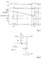
- FIG. 1schematically shows an example of CMOS type photodetector of an image sensor matrix.
- a photodiode Dhas its anode connected to a low reference potential VSS.
- the cathode of photodiode Dis connected to a node SN detection.
- a T1 initialization MOS transistor and a T2 measuring MOS transistor, with N channel,have their drain connected to a high VDD supply potential.
- the source of transistor T1 and the gate of transistor T2are connected to the detection node SN.
- the gate of transistor T1receives an NI control signal SN node initialization.
- a MOS control transistor T3 to channel Nhas its drain connected to the source of transistor T2.
- the gate of transistor T3receives a line selection signal LS.
- the source of transistor T3is connected to a reading means 2.
- the reading means 2receives a read command signal ST.
- Means 2is connected to other photodiodes not shown of the matrix.
- Photodiode D of a photodetector as in Figure 1can be made in the same substrate as the other elements of the photodetector. Its light receiving surface must be sufficient to ensure good detection, the surface occupied by the other elements of the photodetector reducing the number of photons picked up by the photodiode. To increase the surface of the photodiode without increasing the total area of a photodetector, one solution is to make the photodiode above all the other elements of the photodetector.
- FIG. 2schematically shows by way of example a sectional view of a photodiode D and of an initialization MOS transistor T1 of a photodetector, in which the photodiode is formed above the other elements of the photodetector.
- the transistor T1is produced in an active zone 4 of type P delimited by a field isolation zone 8 made of silicon oxide (SiO 2 ).
- a field isolation zone 8made of silicon oxide (SiO 2 ).
- an amorphous silicon layercomprising a lower region 18, an intrinsic intermediate layer 20 and an upper layer 22 of the type P, to constitute a PIN type photodiode.
- the layer 22forms the anode of the photodiode and the region 18 forms the cathode of the photodiode.
- the layer 22is covered with a conductive and transparent layer 24 of ITO connected to the VSS potential.
- the region 18is connected by a conductive via 28 to the source region 12.
- a conductive region 26can be placed under the region 18.
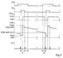
- FIG. 3illustrates, during a phase of measuring the light received by the photodetector of FIG. 1, the time-dependent variations of the LS and NI signals, the potential VSN of the node SN, and of the signal ST.
- the transistor T2is connected in VSN potential follower mounting of node SN.
- the transistor T2has a unit gain and that the potential of the source of transistor T2 is substantially equal to the potential VSN. It is thus considered that the reading means 2, connected to the source of transistor T2 via transistor T3, allows memorizing the VSN potential.
- the selection signal LSis at 1 of such that the transistor T3 is conductive and that the source of transistor T2 is connected to reading means 2.
- the read signal STis at 0 and the read means 2 is inactivated.
- the initialization signal NIis brought to 1, for a short initialization period, so that bring the VSN potential to VDD.
- the NI signalreturns to 0.
- the VSN potentialdrops then of a potential ⁇ V0 due in particular to the capacitive coupling existing between the gate and the source of transistor T1, thus than noise introduced by transistor T1.
- the ST signalis activated for a short time to control the reading of the potential VDD- ⁇ V0 by means 2. From the instant when the transistor T1 is no longer conductive and when the cathode of the photodiode is no longer connected to VDD, and if the photodiode D is subjected to light radiation, electrons accumulate at the cathode of the photodiode. The VSN potential of the cathode then decreases in proportion to the light received.
- the signal LSis brought to 0 so to make the transistor T3 nonconductive and to isolate the photodetector of means 2.
- the means 2can then be connected to another photodetector of the image sensor.
- the LS signalis again brought to 1 and the transistor T3 is made conductive.
- the signal STis briefly activated by so as to control the reading of the VSN potential by means 2.
- the potential VSNthen has a value VDD- ⁇ V0- ⁇ V1, where ⁇ V1 depends the number of photons received by the photodiode and a noise negligible thermal.
- the measurement of VDD- ⁇ V0- ⁇ V1is subtracted from the previous measurement of VDD- ⁇ V0 to find out the value ⁇ V1 and thus the light received by the photodiode between times t1 and t4.
- Amorphous silicon photodiodehas traps charge capable of storing electrons during a so-called relaxation time.
- part of the electrons accumulated in the cathode of the photodiode between the instants t1 and t4is immobilized by the load traps of the photodiode.
- the value ⁇ V1 measured at the end of the measurementdoes not take into account the electrons stored in the load traps, and the measurement is distorted.
- the duration of connection to the VDD potential during the initialization phaseis insufficient to empty all charge traps. So at start of each measurement phase, load traps contain a quantity of parasitic electrons which depends on the light received during one or more measurement phases preceding.
- a known solution to eliminate this phenomenon of dragginginvolves limiting the number of traps in the photodiode D.
- This solutioninvolves making photodiode D in a specifically produced amorphous silicon, and involves an expensive extension of the manufacturing time of the circuit.
- An object of the present inventionis to provide a CMOS photodetector comprising a silicon photodiode amorphous with a simple structure, inexpensive to manufacture, and which does not not give rise to a lagging phenomenon as described previously.
- the present inventionprovides a photodetector comprising a silicon photodiode amorphous whose anode is connected to a reference potential, a initialization MOS transistor connected between the cathode of the photodiode and a first supply potential to put the cathode at the first supply potential during a phase initialization, and means for measuring the potential of the cathode of the photodiode, comprising saturation means to bring the cathode of the photodiode to a potential of saturation close to the reference potential immediately before the initialization phase.
- the source of the initialization MOS transistoris connected to the cathode of the photodiode and the photodetector comprises means proper switch to bring the drain of the MOS transistor initialization at saturation potential or at the first feeding potential.
- the initialization MOS transistoris controlled in regime of weak inversion.
- the initialization MOS transistoris controlled in regime of strong inversion.
- the measuring meansinclude a MOS measuring transistor whose grid is connected to the cathode of the photodiode, and a control MOS transistor connected in series with the MOS transistor of measurement between a second supply potential and a means of reading.
- the first and second supply potentialsare equal.
- FIG. 4schematically represents a circuit of photodetector according to the present invention.
- the photodetectorincludes a PIN type amorphous silicon photodiode D and a transistor T1 as shown in Figure 2.
- the gate of transistor T1receives an NI control signal.
- the drain of transistor T1is connected to a switch 30, controllable by means not shown, provided for bring the drain of transistor T1 to potential VDD or to VSS potential.
- An N-channel T2 measurement MOS transistorhas its drain connected to the potential VDD and its grid connected to the cathode SN of photodiode D.
- a control transistor T3, of type Nis connected between the source of transistor T2 and a reading means 2 controlled by an ST signal.
- the gate of transistor T3receives an LS control signal.
- FIG. 5illustrates, during a phase of measuring the light received by the photodiode of the detector of FIG. 4, the evolution as a function of time of the signals LS and NI, of the potential VD T1 of the drain of the transistor T1, of the VSN potential of the cathode of photodiode D, and of the control signal ST.
- the LS signalis at level 1 so that the transistor T3 is conductive.
- the switch 30is in a state such that the drain of transistor T1 is connected to potential VSS.
- the signal NIis brought to 1 so as to make the transistor T1 conductive and bring the cathode SN of the photodiode at low potential Vraz.
- the Vraz potentialis substantially equal to the potential VSS increased by the voltage of threshold VT of transistor T1. Lower the potential of the cathode SN at potential Vraz is equivalent to supplying a large quantity of electrons at the SN cathode.
- the cathode SNis maintained at Vraz potential up to an instant t1 'for a duration sufficient for the load trap levels of the cathode are "saturated".
- the charge trapsare found in a state of maximum retention determined, whatever the previous illumination of the photodiode. This erases the "memory" of the previous image contained in the traps of the amorphous silicon photodiode.
- the switch 30is commanded to so as to bring the drain of transistor T1 to potential VDD.
- the cathode of the photodiodeis then brought to a potential substantially equal to the VDD potential.
- This stepcorresponds to a initialization of the photodiode before starting a new integration phase.
- the signal NIis brought to 0.
- the potential VSNa voltage ⁇ V0 'then falls due in particular to the coupling capacitive between the gate and the source of transistor T1.
- the means 2is controlled to store the value VDD- ⁇ V0 ' VSN potential.
- the signal LSis brought to 0 of so as to make the transistor T3 nonconductive. Way to reading 2 is then isolated from the photodetector and it can be connected to another photodetector in the matrix.
- the LS signalis brought to 1 so as to make the conductive transistor T3 and to connect the reading means 2 to the photodetector.
- the switch 30is commanded to bring the drain of the transistor to the potential VSS.
- the means 2is controlled to memorize the potential of the node SN, equal to VDD- ⁇ V0'- ⁇ V1 '. All charge traps being initially saturated, the quantity of electrons that they release between times t2 'and t6' is independent of the previous measurement phase (s). If we considers that the quantity of electrons released by the traps does not does not fluctuate over time, the voltage ⁇ V1 'only varies function of the light received by the photodiode between the instants t2 'and t4'. Subtracting measurements from times t6 'and t2' makes it possible to determine the value ⁇ V1 '.
- a photodetector according to the present inventionthus makes it possible to provide a potential whose variation depends only on the light received during each measurement period, which allows remove the lagging phenomenon described above.
- the present inventionhas been described in the case where the quantity of electrons released by the traps do not fluctuate over time. In practice, this amount of electrons can fluctuate and introduce noise temporal in the measurement of the light received by the photodiode.
- the present inventionis capable of various variations and modifications that will appear to humans of career.
- the present inventionhas been described related to a type of amorphous silicon photodiode particular, but the skilled person will easily adapt the present invention to any type of silicon photodiode amorphous, and more generally to any type of photodiode with charge traps.
- the present inventionhas been described in connection with a particular sequencing of the operations of saturation of the traps of photodiode charges, initialization and measure of the potential of the photodiode cathode but man skilled in the art will easily adapt the present invention to other sequences.
- the operation of saturation of the photodiode charge trapscan be performed in the middle of the initialization phase of the the photodiode.
- the durations of the different phasesdid not not specified, but those skilled in the art will determine them without difficulties.
- the present inventionhas been described in connection with all-or-nothing commands, or strong inversion, of the transistor T1, but the person skilled in the art will easily adapt the present invention of low inversion commands for transistor T1, for example to reduce the noise introduced by the transistors.
- the present inventionhas been described in connection with a case where the transistor T2 has a unity gain and where the potential of the source of transistor T2 is substantially equal to VSN potential, but the skilled person will easily adapt the present invention to a case where the transistor T2 has a non-unit gain and where the potential of the transistor source T2 is not equal to the VSN potential.
- the present inventionhas been described in connection with a case in which the drain of transistor T1 can be brought to a high potential VDD identical to the high potential at which the drain of transistor T2 is connected, but those skilled in the art will easily adapt the present invention to a case in which these two high potentials are different.
Landscapes
- Chemical & Material Sciences (AREA)
- Engineering & Computer Science (AREA)
- Nanotechnology (AREA)
- Physics & Mathematics (AREA)
- Life Sciences & Earth Sciences (AREA)
- Biophysics (AREA)
- Optics & Photonics (AREA)
- Crystallography & Structural Chemistry (AREA)
- Transforming Light Signals Into Electric Signals (AREA)
- Photometry And Measurement Of Optical Pulse Characteristics (AREA)
- Light Receiving Elements (AREA)
- Solid State Image Pick-Up Elements (AREA)
Abstract
Translated fromFrenchDescription
Translated fromFrenchLa présente invention concerne la réalisation sousforme monolithique de capteurs d'images destinés à être utilisésdans des dispositifs de prise de vues tels que, par exemple, descaméras, des camescopes ou encore des appareils photographiquesnumériques. Plus particulièrement, la présente inventionconcerne des capteurs d'images réalisés en technologie CMOS.The present invention relates to the realization undermonolithic form of image sensors for usein cameras such as, for example,cameras, camcorders or still camerasdigital. More particularly, the present inventionrelates to image sensors produced in CMOS technology.
Un capteur d'images réalisé en technologie CMOScomprend généralement une matrice de photodétecteurs disposés àl'intersection de lignes et de colonnes.An image sensor made in CMOS technologygenerally comprises an array of photodetectors arranged atthe intersection of rows and columns.
La figure 1 représente schématiquement un exemple dephotodétecteur de type CMOS d'une matrice d'un capteur d'images.Une photodiode D a son anode reliée à un potentiel bas de référenceVSS. La cathode de la photodiode D est reliée à un noeudde détection SN. Un transistor MOS d'initialisation T1 et untransistor MOS de mesure T2, à canal N, ont leur drain relié àun potentiel haut d'alimentation VDD. La source du transistor T1et la grille du transistor T2 sont reliées au noeud de détectionSN. La grille du transistor T1 reçoit un signal NI de commanded'initialisation du noeud SN. Un transistor MOS de commande T3 àcanal N a son drain relié à la source du transistor T2. Lagrille du transistor T3 reçoit un signal de sélection de ligne LS. La source du transistor T3 est reliée à un moyen de lecture2. Le moyen de lecture 2 reçoit un signal de commande de lectureST. Le moyen 2 est relié à d'autres photodiodes non représentéesde la matrice.Figure 1 schematically shows an example ofCMOS type photodetector of an image sensor matrix.A photodiode D has its anode connected to a low reference potentialVSS. The cathode of photodiode D is connected to a nodeSN detection. A T1 initialization MOS transistor and aT2 measuring MOS transistor, with N channel, have their drain connected toa high VDD supply potential. The source of transistor T1and the gate of transistor T2 are connected to the detection nodeSN. The gate of transistor T1 receives an NI control signalSN node initialization. A MOS control transistor T3 tochannel N has its drain connected to the source of transistor T2. Thegate of transistor T3 receives a line selection signalLS. The source of transistor T3 is connected to a reading means2. The reading means 2 receives a read command signalST.
La photodiode D d'un photodétecteur tel qu'en figure 1peut être réalisée dans le même substrat que les autres élémentsdu photodétecteur. Sa surface réceptrice de lumière doit êtresuffisante pour assurer une bonne détection, la surface occupéepar les autres éléments du photodétecteur réduisant le nombre dephotons captés par la photodiode. Pour augmenter la surface dela photodiode sans augmenter la surface totale d'unphotodétecteur, une solution consiste à réaliser la photodiodeau dessus de l'ensemble des autres éléments du photodétecteur.Photodiode D of a photodetector as in Figure 1can be made in the same substrate as the other elementsof the photodetector. Its light receiving surface must besufficient to ensure good detection, the surface occupiedby the other elements of the photodetector reducing the number ofphotons picked up by the photodiode. To increase the surface ofthe photodiode without increasing the total area of aphotodetector, one solution is to make the photodiodeabove all the other elements of the photodetector.
La figure 2 représente schématiquement à titred'exemple une vue en coupe d'une photodiode D et d'un transistorMOS d'initialisation T1 d'un photodétecteur, dans lequel laphotodiode est formée au-dessus des autres éléments duphotodétecteur. Pour des raisons de lisibilité, les figuresreprésentant les différentes régions de semiconducteur ne sontpas tracées à l'échelle. Le transistor T1 est réalisé dans unezone active 4 de type P délimitée par une zone d'isolement dechamp 8 en oxyde de silicium (SiO2). De part et d'autre d'unegrille isolée 10, se trouvent des régions de type N de source 12et de drain 14 du transistor T1. Le transistor T1 est recouvertd'une couche d'isolant (SiO2) 16. Au-dessus de la couche 16 estformée une couche de silicium amorphe comprenant une régioninférieure 18, une couche intermédiaire 20 intrinsèque et unecouche supérieure 22 de type P, pour constituer une photodiodede type PIN. La couche 22 forme l'anode de la photodiode et larégion 18 forme la cathode de la photodiode. La couche 22 estrecouverte d'une couche 24 conductrice et transparente d'ITOreliée au potentiel VSS. La région 18 est reliée par un viaconducteur 28 à la région de source 12. Une région conductrice26 peut être disposée sous la région 18.FIG. 2 schematically shows by way of example a sectional view of a photodiode D and of an initialization MOS transistor T1 of a photodetector, in which the photodiode is formed above the other elements of the photodetector. For reasons of readability, the figures representing the different semiconductor regions are not drawn to scale. The transistor T1 is produced in an
La figure 3 illustre, lors d'une phase de mesure de lalumière reçue par le photodétecteur de la figure 1, lesvariations en fonction du temps des signaux LS et NI, dupotentiel VSN du noeud SN, et du signal ST. Le transistor T2 estconnecté en montage suiveur du potentiel VSN du noeud SN. Pourdes raisons de simplicité, on considère par la suite que letransistor T2 présente un gain unitaire et que le potentiel dela source du transistor T2 est sensiblement égal au potentielVSN. On considère ainsi que le moyen de lecture 2, relié à lasource du transistor T2 par l'intermédiaire du transistor T3,permet de mémoriser le potentiel VSN.FIG. 3 illustrates, during a phase of measuring thelight received by the photodetector of FIG. 1, thetime-dependent variations of the LS and NI signals, thepotential VSN of the node SN, and of the signal ST. The transistor T2 isconnected in VSN potential follower mounting of node SN. Forfor reasons of simplicity, it is subsequently considered that thetransistor T2 has a unit gain and that the potential ofthe source of transistor T2 is substantially equal to the potentialVSN. It is thus considered that the reading means 2, connected to thesource of transistor T2 via transistor T3,allows memorizing the VSN potential.
A un instant t0, le signal de sélection LS est à 1 detelle manière que le transistor T3 est conducteur et que lasource du transistor T2 est reliée au moyen de lecture 2. Lesignal de lecture ST est à 0 et le moyen de lecture 2 estinactivé. A l'instant t0, le signal d'initialisation NI estamené à 1, pour une brève durée d'initialisation, de manière àamener le potentiel VSN à VDD. A l'issue de cetteinitialisation, le signal NI revient à 0. Le potentiel VSN chutealors d'un potentiel ΔV0 dû notamment au couplage capacitifexistant entre la grille et la source du transistor T1, ainsiqu'à du bruit introduit par le transistor T1.At an instant t0, the selection signal LS is at 1 ofsuch that the transistor T3 is conductive and that thesource of transistor T2 is connected to reading means 2. Theread signal ST is at 0 and the
A un instant t1, après que le signal NI est revenu à0, le signal ST est activé un bref instant pour commander lalecture du potentiel VDD-ΔV0 par le moyen 2. A partir del'instant où le transistor T1 n'est plus conducteur et où lacathode de la photodiode n'est plus reliée à VDD, et si laphotodiode D est soumise à un rayonnement lumineux, desélectrons viennent s'accumuler au niveau de la cathode de laphotodiode. Le potentiel VSN de la cathode décroít alorsproportionnellement à la lumière reçue.At an instant t1, after the signal NI has returned to0, the ST signal is activated for a short time to control thereading of the potential VDD-ΔV0 by
A un instant t2, le signal LS est amené à 0 de manièreà rendre le transistor T3 non conducteur et à isoler le photodétecteurdu moyen 2. Le moyen 2 peut alors être relié à un autrephotodétecteur du capteur d'images.At an instant t2, the signal LS is brought to 0 soto make the transistor T3 nonconductive and to isolate the photodetectorof
A un instant t3, après une durée prédéterminée pendantlaquelle la photodiode est soumise à un rayonnement lumineux quel'on veut mesurer, le signal LS est à nouveau amené à 1 et letransistor T3 est rendu conducteur.At an instant t3, after a predetermined duration forwhich the photodiode is subjected to a light radiation thatwe want to measure, the LS signal is again brought to 1 and thetransistor T3 is made conductive.
A un instant t4, le signal ST est brièvement activé demanière à commander la lecture du potentiel VSN par le moyen 2.Le potentiel VSN a alors une valeur VDD-ΔV0-ΔV1, où ΔV1 dépenddu nombre de photons reçus par la photodiode et d'un bruitthermique négligeable. La mesure de VDD-ΔV0-ΔV1 est soustraite àla mesure précédente de VDD-ΔV0 pour connaítre la valeur ΔV1 etainsi la lumière reçue par la photodiode entre les instants t1et t4.At time t4, the signal ST is briefly activated byso as to control the reading of the VSN potential by
Une photodiode en silicium amorphe comporte des piègesde charge susceptibles de stocker des électrons pendant unedurée dite temps de relaxation. Lors de chaque phase de mesurede lumière telle que décrite en figure 3, une partie desélectrons accumulés dans la cathode de la photodiode entre lesinstants t1 et t4 se trouve immobilisée par les pièges de chargede la photodiode. La valeur ΔV1 mesurée à l'issue de la phase demesure ne prend pas en compte les électrons stockés dans lespièges de charge, et la mesure est faussée. En outre, la duréede connexion au potentiel VDD pendant la phase d'initialisationest insuffisante pour vider tous les pièges de charge. Ainsi, audébut de chaque phase de mesure, des pièges de chargecontiennent une quantité d'électrons parasites qui dépend de lalumière reçue lors d'une ou plusieurs phases de mesureprécédentes. Ces électrons parasites, libérés à l'issue du tempsde relaxation des pièges de charge, faussent la valeur ΔV1mesurée. La valeur ΔV1 mesurée à l'issue de chaque phase demesure dépend ainsi en partie de la lumière reçue lors de la oudes phases de mesure précédentes. Dans un capteur d'imagescomprenant une matrice de photodétecteurs, ce phénomène derétention des électrons donne lieu à une rémanence ou à untraínage de l'image. L'importance du traínage dépend notamment de la quantité de pièges dans la photodiode et de la duréemoyenne de rétention des électrons par ces pièges.Amorphous silicon photodiode has trapscharge capable of storing electrons during aso-called relaxation time. During each measurement phaseof light as described in FIG. 3, part of theelectrons accumulated in the cathode of the photodiode between theinstants t1 and t4 is immobilized by the load trapsof the photodiode. The value ΔV1 measured at the end of themeasurement does not take into account the electrons stored in theload traps, and the measurement is distorted. In addition, the durationof connection to the VDD potential during the initialization phaseis insufficient to empty all charge traps. So atstart of each measurement phase, load trapscontain a quantity of parasitic electrons which depends on thelight received during one or more measurement phasespreceding. These parasitic electrons, released at the end of timeload trap relaxation, distort the value ΔV1measured. The value ΔV1 measured at the end of each phase ofmeasurement thus partly depends on the light received during the orprevious measurement phases. In an image sensorcomprising a matrix of photodetectors, this phenomenon ofelectron retention gives rise to remanence orimage dragging. The importance of the drag depends in particularthe quantity of traps in the photodiode and the durationaverage electron retention by these traps.
Une solution connue pour supprimer ce phénomène detraínage consiste à limiter le nombre de pièges dans la photodiodeD. Cette solution implique de réaliser la photodiode Ddans un silicium amorphe réalisé de façon spécifique, etimplique un allongement coûteux de la durée de fabrication ducircuit.A known solution to eliminate this phenomenon ofdragging involves limiting the number of traps in the photodiodeD. This solution involves making photodiode Din a specifically produced amorphous silicon, andinvolves an expensive extension of the manufacturing time of thecircuit.
Un objet de la présente invention est de prévoir unphotodétecteur CMOS comportant une photodiode en siliciumamorphe de structure simple, peu coûteux à fabriquer, et qui nedonne pas lieu à un phénomène de traínage tel que décritprécédemment.An object of the present invention is to provide aCMOS photodetector comprising a silicon photodiodeamorphous with a simple structure, inexpensive to manufacture, and which does notnot give rise to a lagging phenomenon as describedpreviously.
Pour atteindre cet objet, la présente inventionprévoit un photodétecteur comportant une photodiode en siliciumamorphe dont l'anode est reliée à un potentiel de référence, untransistor MOS d'initialisation connecté entre la cathode de laphotodiode et un premier potentiel d'alimentation pour mettre lacathode au premier potentiel d'alimentation pendant une phased'initialisation, et des moyens de mesure du potentiel de lacathode de la photodiode, comprenant des moyens de saturationpour amener la cathode de la photodiode à un potentiel desaturation proche du potentiel de référence immédiatement avantla phase d'initialisation.To achieve this object, the present inventionprovides a photodetector comprising a silicon photodiodeamorphous whose anode is connected to a reference potential, ainitialization MOS transistor connected between the cathode of thephotodiode and a first supply potential to put thecathode at the first supply potential during a phaseinitialization, and means for measuring the potential of thecathode of the photodiode, comprising saturation meansto bring the cathode of the photodiode to a potential ofsaturation close to the reference potential immediately beforethe initialization phase.
Selon un mode de réalisation de la présente invention,la source du transistor MOS d'initialisation est reliée à lacathode de la photodiode et le photodétecteur comprend un moyend'aiguillage propre à amener le drain du transistor MOSd'initialisation au potentiel de saturation ou au premierpotentiel d'alimentation.According to an embodiment of the present invention,the source of the initialization MOS transistor is connected to thecathode of the photodiode and the photodetector comprises meansproper switch to bring the drain of the MOS transistorinitialization at saturation potential or at the firstfeeding potential.
Selon un mode de réalisation de la présente invention,le transistor MOS d'initialisation est commandé en régime defaible inversion.According to an embodiment of the present invention,the initialization MOS transistor is controlled in regime ofweak inversion.
Selon un mode de réalisation de la présente invention,le transistor MOS d'initialisation est commandé en régime deforte inversion.According to an embodiment of the present invention,the initialization MOS transistor is controlled in regime ofstrong inversion.
Selon un mode de réalisation de la présente invention,les moyens de mesure comprennent un transistor MOS de mesuredont la grille est reliée à la cathode de la photodiode, et untransistor MOS de commande relié en série avec le transistor MOSde mesure entre un second potentiel d'alimentation et un moyende lecture.According to an embodiment of the present invention,the measuring means include a MOS measuring transistorwhose grid is connected to the cathode of the photodiode, and acontrol MOS transistor connected in series with the MOS transistorof measurement between a second supply potential and a meansof reading.
Selon un mode de réalisation de la présente invention,les premier et second potentiels d'alimentation sont égaux.According to an embodiment of the present invention,the first and second supply potentials are equal.
La présente invention vise également un procédé demesure de la lumière reçue par un photodétecteur comportant unephotodiode en silicium amorphe dont l'anode est reliée à unpotentiel de référence, comportant les étapes successivesconsistant à :
Ces objets, caractéristiques et avantages, ainsi qued'autres de la présente invention seront exposés en détail dansla description suivante de modes de réalisation particuliersfaite à titre non-limitatif en relation avec les figures jointesparmi lesquelles :
De mêmes éléments ont été désignés par les mêmes référencesaux différentes figures. Seuls les éléments nécessaires àla compréhension de la présente invention ont été représentésaux différentes figures.Same elements have been designated by the same referencesto the different figures. Only the elements necessary forunderstanding of the present invention have been shownto the different figures.
La figure 4 représente schématiquement un circuit dephotodétecteur selon la présente invention. Le photodétecteurcomprend une photodiode D en silicium amorphe de type PIN et untransistor T1 tels que représentés en figure 2. La grille dutransistor T1 reçoit un signal de commande NI. Selon la présenteinvention, le drain du transistor T1 est relié à un aiguilleur30, commandable par des moyens non représentés, prévu pouramener le drain du transistor T1 au potentiel VDD ou aupotentiel VSS. Un transistor MOS de mesure T2 à canal N a sondrain relié au potentiel VDD et sa grille reliée à la cathode SNde la photodiode D. Un transistor de commande T3, de type N estconnecté entre la source du transistor T2 et un moyen de lecture2 commandé par un signal ST. La grille du transistor T3 reçoitun signal de commande LS.FIG. 4 schematically represents a circuit ofphotodetector according to the present invention. The photodetectorincludes a PIN type amorphous silicon photodiode D and atransistor T1 as shown in Figure 2. The gate oftransistor T1 receives an NI control signal. According to thisinvention, the drain of transistor T1 is connected to a
La figure 5 illustre, lors d'une phase de mesure de lalumière reçue par la photodiode du détecteur de la figure 4,l'évolution en fonction du temps des signaux LS et NI, du potentielVDT1 du drain du transistor T1, du potentiel VSN de lacathode de la photodiode D, et du signal de commande ST.FIG. 5 illustrates, during a phase of measuring the light received by the photodiode of the detector of FIG. 4, the evolution as a function of time of the signals LS and NI, of the potential VDT1 of the drain of the transistor T1, of the VSN potential of the cathode of photodiode D, and of the control signal ST.
A un instant t0', au début de la phase de mesure, lesignal LS est à un niveau 1 de telle manière que le transistorT3 est conducteur. L'aiguilleur 30 est dans un état tel que le drain du transistor T1 est relié au potentiel VSS. A l'instantt0', le signal NI est amené à 1 de manière à rendre letransistor T1 conducteur et à amener la cathode SN de laphotodiode à un potentiel bas Vraz. Le potentiel Vraz estsensiblement égal au potentiel VSS augmenté de la tension deseuil VT du transistor T1. Abaisser le potentiel de la cathodeSN au potentiel Vraz équivaut à fournir une grande quantitéd'électrons à la cathode SN. La cathode SN est maintenue aupotentiel Vraz jusqu'à un instant t1' pendant une duréesuffisante pour que les niveaux de pièges de charge de lacathode soient "saturés". Ainsi, à chaque instant t1', lespièges de charge se retrouvent dans un état de rétention maximumdéterminé, quel qu'ait été l'éclairement antérieur de laphotodiode. On efface ainsi la "mémoire" de l'image précédentecontenue dans les pièges de la photodiode de silicium amorphe.At an instant t0 ', at the start of the measurement phase, theLS signal is at level 1 so that the transistorT3 is conductive. The
A l'instant t1', l'aiguilleur 30 est commandé demanière à amener le drain du transistor T1 au potentiel VDD. Lacathode de la photodiode est alors amenée à un potentiel sensiblementégal au potentiel VDD. Cette étape correspond à uneinitialisation de la photodiode avant que ne démarre unenouvelle phase d'intégration. Après une durée d'initialisationprédéterminée, le signal NI est amené à 0. Le potentiel VSNchute alors d'une tension ΔV0' due notamment au couplagecapacitif entre la grille et la source du transistor T1.At time t1 ', the
A un instant t2', peu après que le signal NI ait étéamené à 0, le moyen 2 est commandé pour mémoriser la valeur VDD-ΔV0'du potentiel VSN.At an instant t2 ', shortly after the signal NI has beenbrought to 0, the
A un instant t3', le signal LS est amené à 0 demanière à rendre le transistor T3 non conducteur. Le moyen delecture 2 est alors isolé du photodétecteur et il peut êtreconnecté à un autre photodétecteur de la matrice.At an instant t3 ', the signal LS is brought to 0 ofso as to make the transistor T3 nonconductive. Way toreading 2 is then isolated from the photodetector and it can beconnected to another photodetector in the matrix.
A un instant t4', après une durée prédéterminéependant laquelle la photodiode est soumise à un rayonnementlumineux, le signal LS est amené à 1 de manière à rendre le transistor T3 conducteur et à relier le moyen de lecture 2 auphotodétecteur.At an instant t4 ', after a predetermined durationduring which the photodiode is subjected to radiationluminous, the LS signal is brought to 1 so as to make theconductive transistor T3 and to connect the reading means 2 to thephotodetector.
A un instant t5', l'aiguilleur 30 est commandé pouramener le drain du transistor au potentiel VSS.At an instant t5 ′, the
A un instant t6', le moyen 2 est commandé pour mémoriserle potentiel du noeud SN, égal à VDD-ΔV0'-ΔV1'. Tous lespièges de charge étant initialement saturés, la quantité d'électronsqu'ils libèrent entre les instants t2' et t6' estindépendante de la ou des phases de mesure précédentes. Si l'onconsidère que la quantité d'électrons libérée par les pièges nefluctue pas avec le temps, la tension ΔV1' ne varie qu'enfonction de la lumière reçue par la photodiode entre lesinstants t2' et t4'. La soustraction des mesures faites auxinstants t6' et t2' permet de déterminer la valeur ΔV1'. Unphotodétecteur selon la présente invention permet ainsi defournir un potentiel dont la variation ne dépend que de lalumière reçue pendant chaque période de mesure, ce qui permet desupprimer le phénomène de traínage exposé précédemment.At an instant t6 ', the
Pour des raisons de simplicité, la présente inventiona été décrite dans le cas où la quantité d'électrons libérée parles pièges ne fluctue pas avec le temps. En pratique, cettequantité d'électrons peut fluctuer et introduire un bruittemporel dans la mesure de la lumière reçue par la photodiode.For reasons of simplicity, the present inventionhas been described in the case where the quantity of electrons released bythe traps do not fluctuate over time. In practice, thisamount of electrons can fluctuate and introduce noisetemporal in the measurement of the light received by the photodiode.
Pour des raisons de simplicité, la présente inventiona été décrite dans le cas où le potentiel Vraz permet de saturerl'ensemble des pièges de charge de la cathode de la photodiode.En pratique, une quasi-saturation suffira.For reasons of simplicity, the present inventionhas been described in the case where the Vraz potential allows saturationall of the photodiode cathode charge traps.In practice, a quasi-saturation will suffice.
Bien entendu, la présente invention est susceptible dediverses variantes et modifications qui apparaítront à l'hommedu métier. En particulier, la présente invention a été décriteen relation avec un type de photodiode en silicium amorpheparticulier, mais l'homme du métier adaptera sans difficultés laprésente invention à tout type de photodiode en siliciumamorphe, et plus généralement à tout type de photodiodecomportant des pièges de charge.Of course, the present invention is capable ofvarious variations and modifications that will appear to humansof career. In particular, the present invention has been describedrelated to a type of amorphous silicon photodiodeparticular, but the skilled person will easily adapt thepresent invention to any type of silicon photodiodeamorphous, and more generally to any type of photodiodewith charge traps.
La présente invention a été décrite en relation avecun séquencement particulier des opérations de saturation despièges de charges de la photodiode, d'initialisation et demesure du potentiel de la cathode de la photodiode, mais l'hommedu métier adaptera sans difficultés la présente invention àd'autres séquencements. A titre d'exemple, l'opération desaturation des pièges de charge de la photodiode peut êtreréalisée au milieu de la phase d'initialisation du potentiel dela photodiode. De même, les durées des différentes phases n'ontpas été précisées, mais l'homme du métier les déterminera sansdifficultés.The present invention has been described in connection witha particular sequencing of the operations of saturation of thetraps of photodiode charges, initialization andmeasure of the potential of the photodiode cathode but manskilled in the art will easily adapt the present invention toother sequences. For example, the operation ofsaturation of the photodiode charge traps can beperformed in the middle of the initialization phase of thethe photodiode. Similarly, the durations of the different phases did notnot specified, but those skilled in the art will determine them withoutdifficulties.
La présente invention a été décrite en relation avecdes commandes en tout-ou-rien, ou forte inversion, du transistorT1, mais l'homme du métier adaptera sans difficultés la présenteinvention à des commandes en faible inversion du transistor T1,par exemple pour réduire le bruit introduit par les transistors.The present invention has been described in connection withall-or-nothing commands, or strong inversion, of the transistorT1, but the person skilled in the art will easily adapt the presentinvention of low inversion commands for transistor T1,for example to reduce the noise introduced by the transistors.
La présente invention a été décrite en relation avecun cas où le transistor T2 présente un gain unitaire et où lepotentiel de la source du transistor T2 est sensiblement égal aupotentiel VSN, mais l'homme du métier adaptera sans difficultésla présente invention à un cas où le transistor T2 présente ungain non unitaire et où le potentiel de la source du transistorT2 n'est pas égal au potentiel VSN.The present invention has been described in connection witha case where the transistor T2 has a unity gain and where thepotential of the source of transistor T2 is substantially equal toVSN potential, but the skilled person will easily adaptthe present invention to a case where the transistor T2 has anon-unit gain and where the potential of the transistor sourceT2 is not equal to the VSN potential.
La présente invention a été décrite en relation avecdes transistors à canal N, mais l'homme du métier adaptera sansdifficultés la présente invention à des transistors à canal P.The present invention has been described in connection withN-channel transistors, but those skilled in the art will adapt withoutdifficulties of the present invention with P channel transistors
La présente invention a été décrite en relation avecun cas dans lequel le drain du transistor T1 peut être amené àun potentiel haut VDD identique au potentiel haut auquel ledrain du transistor T2 est relié, mais l'homme du métieradaptera sans difficultés la présente invention à un cas danslequel ces deux potentiels hauts sont différents.The present invention has been described in connection witha case in which the drain of transistor T1 can be brought toa high potential VDD identical to the high potential at which thedrain of transistor T2 is connected, but those skilled in the artwill easily adapt the present invention to a case inwhich these two high potentials are different.
Claims (7)
Translated fromFrenchApplications Claiming Priority (2)
| Application Number | Priority Date | Filing Date | Title |
|---|---|---|---|
| FR0106131AFR2824664A1 (en) | 2001-05-09 | 2001-05-09 | CMOS PHOTODETECTOR COMPRISING AN AMORPHOUS SILICON PHOTODIODE |
| FR0106131 | 2001-05-09 |
Publications (2)
| Publication Number | Publication Date |
|---|---|
| EP1256984A2true EP1256984A2 (en) | 2002-11-13 |
| EP1256984A3 EP1256984A3 (en) | 2002-12-18 |
Family
ID=8863086
Family Applications (1)
| Application Number | Title | Priority Date | Filing Date |
|---|---|---|---|
| EP02354079AWithdrawnEP1256984A3 (en) | 2001-05-09 | 2002-05-07 | CMOS photodetector comprising an amorphous silicon photodiode |
Country Status (4)
| Country | Link |
|---|---|
| US (1) | US6831264B2 (en) |
| EP (1) | EP1256984A3 (en) |
| JP (1) | JP2002369085A (en) |
| FR (1) | FR2824664A1 (en) |
Cited By (2)
| Publication number | Priority date | Publication date | Assignee | Title |
|---|---|---|---|---|
| RU2262775C2 (en)* | 2003-06-24 | 2005-10-20 | Институт проблем проектирования в микроэлектронике РАН | Cmos photodetector cell |
| EP2249389A2 (en) | 2004-02-25 | 2010-11-10 | S.O.I. Tec Silicon on Insulator Technologies | Photodetecting device |
Families Citing this family (14)
| Publication number | Priority date | Publication date | Assignee | Title |
|---|---|---|---|---|
| US20050140634A1 (en)* | 2003-12-26 | 2005-06-30 | Nec Corporation | Liquid crystal display device, and method and circuit for driving liquid crystal display device |
| JP5054509B2 (en)* | 2004-02-25 | 2012-10-24 | ソワテク | Photodetector |
| JP4093220B2 (en)* | 2004-10-05 | 2008-06-04 | コニカミノルタホールディングス株式会社 | Solid-state imaging device and imaging device including the solid-state imaging device |
| US7355222B2 (en)* | 2005-05-19 | 2008-04-08 | Micron Technology, Inc. | Imaging device having a pixel cell with a transparent conductive interconnect line and the method of making the pixel cell |
| KR100744118B1 (en)* | 2005-12-13 | 2007-08-01 | 삼성전자주식회사 | An image sensor having a saturation level detection circuit of the image sensor, a saturation level detection method of the image sensor, and a saturation level detection circuit. |
| FR2901263B1 (en)* | 2006-05-18 | 2008-10-03 | Commissariat Energie Atomique | MOTION-SENSITIVE DEVICE COMPRISING AT LEAST ONE TRANSISTOR |
| US7741657B2 (en)* | 2006-07-17 | 2010-06-22 | Intel Corporation | Inverted planar avalanche photodiode |
| JP2009065161A (en)* | 2007-09-07 | 2009-03-26 | Dongbu Hitek Co Ltd | Image sensor and manufacturing method thereof |
| RU2361322C1 (en)* | 2007-11-29 | 2009-07-10 | Институт проблем проектирования в микроэлектронике Российской академии наук | Method of making cmos photodiode structure, which weighs output signal |
| US8384012B2 (en)* | 2009-05-11 | 2013-02-26 | Infineon Technologies Ag | Photodiode comprising polarizer |
| KR101733755B1 (en) | 2010-01-15 | 2017-05-08 | 가부시키가이샤 한도오따이 에네루기 켄큐쇼 | Semiconductor device and electronic device |
| RU2517917C2 (en)* | 2012-07-20 | 2014-06-10 | Федеральное государственное автономное образовательное учреждение высшего профессионального образования "Национальный исследовательский технологический университет "МИСиС" | Functionally integrated photosensitive matrix cell |
| CN110112138A (en)* | 2019-04-11 | 2019-08-09 | 深圳市华星光电半导体显示技术有限公司 | A kind of sensor devices, tft array substrate and its display panel |
| GB202019768D0 (en) | 2020-12-15 | 2021-01-27 | Ams Ag | Circuit for high-sensitivity radiation sensing |
Citations (2)
| Publication number | Priority date | Publication date | Assignee | Title |
|---|---|---|---|---|
| EP0367650A1 (en)* | 1988-10-25 | 1990-05-09 | Thomson-Csf | Photosensitive device with signal amplification at the photosensitive points |
| US6046444A (en)* | 1997-12-08 | 2000-04-04 | Intel Corporation | High sensitivity active pixel with electronic shutter |
Family Cites Families (5)
| Publication number | Priority date | Publication date | Assignee | Title |
|---|---|---|---|---|
| US6133563A (en)* | 1997-09-29 | 2000-10-17 | Intel Corporation | Sensor cell having a soft saturation circuit |
| EP0928101A3 (en)* | 1997-12-31 | 2001-05-02 | Texas Instruments Incorporated | CMOS area array sensors |
| JP4200545B2 (en)* | 1998-06-08 | 2008-12-24 | ソニー株式会社 | Solid-state imaging device, driving method thereof, and camera system |
| US6252218B1 (en)* | 1999-02-02 | 2001-06-26 | Agilent Technologies, Inc | Amorphous silicon active pixel sensor with rectangular readout layer in a hexagonal grid layout |
| JP3621844B2 (en)* | 1999-02-24 | 2005-02-16 | シャープ株式会社 | Amplification type solid-state imaging device |
- 2001
- 2001-05-09FRFR0106131Apatent/FR2824664A1/enactivePending
- 2002
- 2002-05-07EPEP02354079Apatent/EP1256984A3/ennot_activeWithdrawn
- 2002-05-08JPJP2002132608Apatent/JP2002369085A/ennot_activeWithdrawn
- 2002-05-08USUS10/142,262patent/US6831264B2/ennot_activeExpired - Lifetime
Patent Citations (3)
| Publication number | Priority date | Publication date | Assignee | Title |
|---|---|---|---|---|
| EP0367650A1 (en)* | 1988-10-25 | 1990-05-09 | Thomson-Csf | Photosensitive device with signal amplification at the photosensitive points |
| US6046444A (en)* | 1997-12-08 | 2000-04-04 | Intel Corporation | High sensitivity active pixel with electronic shutter |
| US6380530B1 (en)* | 1997-12-08 | 2002-04-30 | Intel Corporation | Method for operating a high sensitivity active pixel |
Cited By (3)
| Publication number | Priority date | Publication date | Assignee | Title |
|---|---|---|---|---|
| RU2262775C2 (en)* | 2003-06-24 | 2005-10-20 | Институт проблем проектирования в микроэлектронике РАН | Cmos photodetector cell |
| EP2249389A2 (en) | 2004-02-25 | 2010-11-10 | S.O.I. Tec Silicon on Insulator Technologies | Photodetecting device |
| EP2249389B1 (en)* | 2004-02-25 | 2019-02-20 | Sony Semiconductor Solutions Corporation | Method of manufacturing a photodetecting device |
Also Published As
| Publication number | Publication date |
|---|---|
| US6831264B2 (en) | 2004-12-14 |
| US20020185589A1 (en) | 2002-12-12 |
| EP1256984A3 (en) | 2002-12-18 |
| JP2002369085A (en) | 2002-12-20 |
| FR2824664A1 (en) | 2002-11-15 |
Similar Documents
| Publication | Publication Date | Title |
|---|---|---|
| EP0364351B1 (en) | Method of photoelectric detection with reduction of accumulated charges in phototransistors, especially those of the nipin type | |
| EP1256984A2 (en) | CMOS photodetector comprising an amorphous silicon photodiode | |
| US7420154B2 (en) | Pixel circuit with non-destructive readout circuit and methods of operation thereof | |
| EP0367650B1 (en) | Photosensitive device with signal amplification at the photosensitive points | |
| EP0489724B1 (en) | Device and method of photoelectrically converting light into electrical signal | |
| JP3546985B2 (en) | Amplifying photoelectric conversion element, amplifying solid-state imaging device, and method of driving the same | |
| FR2888989A1 (en) | IMAGE SENSOR | |
| FR2820883A1 (en) | HIGH CAPACITY PHOTODIODE | |
| FR2563657A1 (en) | SEMICONDUCTOR IMAGE SENSOR ELEMENT AND IMAGE ANALYZER HAVING THE SAME | |
| EP1231642A1 (en) | Three-transistor photodetector | |
| EP0331546B1 (en) | Photosensitive matrix with two diodes at each point, without any specific reset lead | |
| EP2312832B1 (en) | Pixel circuit in image sensor | |
| EP3487167B1 (en) | Image sensor with high dynamic range | |
| FR2846147A1 (en) | ORDERING A PHOTOSENSITIVE CELL | |
| FR2513015A1 (en) | CHARGE TRANSFER TYPE COLOR IMAGE DETECTION DEVICE | |
| EP0958545B1 (en) | Circuit for integrating light-induced charges with improved linearity | |
| US20050007473A1 (en) | Reducing image sensor lag | |
| JP2006120685A (en) | Imaging device with embedded photodiode structure | |
| US12068353B2 (en) | Imaging device | |
| WO2009068526A1 (en) | Image sensor having four-transistor or five-transistor pixels with reset noise reduction | |
| EP0068947A1 (en) | Light detector device, adapted charge transfer reader and imager using such a device | |
| FR2824665A1 (en) | CMOS TYPE PHOTODETECTOR | |
| EP4440136A1 (en) | Electronic image acquisition circuit | |
| EP1473928A1 (en) | Photosensitive cell control | |
| JPH09121305A (en) | Method and device for driving infrared solid-state imaging device |
Legal Events
| Date | Code | Title | Description |
|---|---|---|---|
| PUAI | Public reference made under article 153(3) epc to a published international application that has entered the european phase | Free format text:ORIGINAL CODE: 0009012 | |
| PUAL | Search report despatched | Free format text:ORIGINAL CODE: 0009013 | |
| AK | Designated contracting states | Kind code of ref document:A2 Designated state(s):AT BE CH CY DE DK ES FI FR GB GR IE IT LI LU MC NL PT SE TR | |
| AX | Request for extension of the european patent | Free format text:AL;LT;LV;MK;RO;SI | |
| AK | Designated contracting states | Kind code of ref document:A3 Designated state(s):AT BE CH CY DE DK ES FI FR GB GR IE IT LI LU MC NL PT SE TR | |
| AX | Request for extension of the european patent | Free format text:AL;LT;LV;MK;RO;SI | |
| RIC1 | Information provided on ipc code assigned before grant | Free format text:7H 04N 3/15 A, 7H 01L 27/146 B, 7H 01L 31/0352 B, 7H 01L 31/0376 B | |
| 17P | Request for examination filed | Effective date:20030616 | |
| AKX | Designation fees paid | Designated state(s):DE FR GB IT | |
| STAA | Information on the status of an ep patent application or granted ep patent | Free format text:STATUS: THE APPLICATION IS DEEMED TO BE WITHDRAWN | |
| 18D | Application deemed to be withdrawn | Effective date:20081107 |