EP1236245B1 - Multi-beam antenna - Google Patents
Multi-beam antennaDownload PDFInfo
- Publication number
- EP1236245B1 EP1236245B1EP00980567AEP00980567AEP1236245B1EP 1236245 B1EP1236245 B1EP 1236245B1EP 00980567 AEP00980567 AEP 00980567AEP 00980567 AEP00980567 AEP 00980567AEP 1236245 B1EP1236245 B1EP 1236245B1
- Authority
- EP
- European Patent Office
- Prior art keywords
- antenna
- contour
- electromagnetic lens
- dielectric substrate
- electromagnetic
- Prior art date
- Legal status (The legal status is an assumption and is not a legal conclusion. Google has not performed a legal analysis and makes no representation as to the accuracy of the status listed.)
- Expired - Lifetime
Links
- 239000000758substrateSubstances0.000claimsdescription49
- 230000005540biological transmissionEffects0.000claimsdescription9
- 230000000644propagated effectEffects0.000claimsdescription7
- 239000004020conductorSubstances0.000claimsdescription2
- 239000000463materialSubstances0.000description4
- 239000000654additiveSubstances0.000description3
- 230000000996additive effectEffects0.000description3
- 238000003486chemical etchingMethods0.000description3
- 238000004891communicationMethods0.000description3
- 230000008021depositionEffects0.000description3
- 238000005516engineering processMethods0.000description3
- 238000003475laminationMethods0.000description3
- 238000000034methodMethods0.000description3
- 238000012545processingMethods0.000description3
- 238000000992sputter etchingMethods0.000description3
- 239000000126substanceSubstances0.000description3
- -1RexoliteTMSubstances0.000description2
- 239000004809TeflonSubstances0.000description2
- 239000002131composite materialSubstances0.000description2
- 230000005855radiationEffects0.000description2
- 239000004593EpoxySubstances0.000description1
- 239000004698PolyethyleneSubstances0.000description1
- 239000004793PolystyreneSubstances0.000description1
- 238000010521absorption reactionMethods0.000description1
- 229910010293ceramic materialInorganic materials0.000description1
- 238000013461designMethods0.000description1
- 239000011152fibreglassSubstances0.000description1
- 238000003384imaging methodMethods0.000description1
- 230000003116impacting effectEffects0.000description1
- 238000004519manufacturing processMethods0.000description1
- 238000012986modificationMethods0.000description1
- 230000004048modificationEffects0.000description1
- 238000004806packaging method and processMethods0.000description1
- 229920000573polyethylenePolymers0.000description1
- 229920002223polystyrenePolymers0.000description1
Images


Classifications
- H—ELECTRICITY
- H01—ELECTRIC ELEMENTS
- H01Q—ANTENNAS, i.e. RADIO AERIALS
- H01Q3/00—Arrangements for changing or varying the orientation or the shape of the directional pattern of the waves radiated from an antenna or antenna system
- H01Q3/24—Arrangements for changing or varying the orientation or the shape of the directional pattern of the waves radiated from an antenna or antenna system varying the orientation by switching energy from one active radiating element to another, e.g. for beam switching
- H01Q3/242—Circumferential scanning
- H—ELECTRICITY
- H01—ELECTRIC ELEMENTS
- H01Q—ANTENNAS, i.e. RADIO AERIALS
- H01Q15/00—Devices for reflection, refraction, diffraction or polarisation of waves radiated from an antenna, e.g. quasi-optical devices
- H01Q15/02—Refracting or diffracting devices, e.g. lens, prism
- H01Q15/04—Refracting or diffracting devices, e.g. lens, prism comprising wave-guiding channel or channels bounded by effective conductive surfaces substantially perpendicular to the electric vector of the wave, e.g. parallel-plate waveguide lens
- H—ELECTRICITY
- H01—ELECTRIC ELEMENTS
- H01Q—ANTENNAS, i.e. RADIO AERIALS
- H01Q19/00—Combinations of primary active antenna elements and units with secondary devices, e.g. with quasi-optical devices, for giving the antenna a desired directional characteristic
- H01Q19/06—Combinations of primary active antenna elements and units with secondary devices, e.g. with quasi-optical devices, for giving the antenna a desired directional characteristic using refracting or diffracting devices, e.g. lens
- H01Q19/062—Combinations of primary active antenna elements and units with secondary devices, e.g. with quasi-optical devices, for giving the antenna a desired directional characteristic using refracting or diffracting devices, e.g. lens for focusing
- H—ELECTRICITY
- H01—ELECTRIC ELEMENTS
- H01Q—ANTENNAS, i.e. RADIO AERIALS
- H01Q21/00—Antenna arrays or systems
- H01Q21/0006—Particular feeding systems
- H01Q21/0031—Parallel-plate fed arrays; Lens-fed arrays
- H—ELECTRICITY
- H01—ELECTRIC ELEMENTS
- H01Q—ANTENNAS, i.e. RADIO AERIALS
- H01Q25/00—Antennas or antenna systems providing at least two radiating patterns
- H01Q25/007—Antennas or antenna systems providing at least two radiating patterns using two or more primary active elements in the focal region of a focusing device
- H01Q25/008—Antennas or antenna systems providing at least two radiating patterns using two or more primary active elements in the focal region of a focusing device lens fed multibeam arrays
- H—ELECTRICITY
- H01—ELECTRIC ELEMENTS
- H01Q—ANTENNAS, i.e. RADIO AERIALS
- H01Q3/00—Arrangements for changing or varying the orientation or the shape of the directional pattern of the waves radiated from an antenna or antenna system
- H01Q3/24—Arrangements for changing or varying the orientation or the shape of the directional pattern of the waves radiated from an antenna or antenna system varying the orientation by switching energy from one active radiating element to another, e.g. for beam switching
- H01Q3/245—Arrangements for changing or varying the orientation or the shape of the directional pattern of the waves radiated from an antenna or antenna system varying the orientation by switching energy from one active radiating element to another, e.g. for beam switching in the focal plane of a focussing device
Definitions
- the instant inventiongenerally relates to a multi-beam antenna comprising an electromagnetic lens and a plurality of antenna feed elements.
- Known waveguide based antennaswhile relatively efficient, are bulky and relatively expensive to manufacture.
- Known phased array antennasare relatively compact but are relatively inefficient.
- Known focal plane antennasare compact but offer a comparatively narrow field of view.
- US 5,583,511discloses a stepped beam active array antenna comprising a feed array that includes a dielectric substrate and a plurality of radiating elements disposed on the substrate.
- the radiating elementsare disposed along a straight edge of the substrate which cooperate with a planar surface of an associated plano-convex lens.
- the focal plane of a disclosed transmit antenna embodimentis fully sampled.
- a stepped beam focal plane receive antennais also disclosed.
- WO 92/13373upon which the precharacterzing portion of appended claim 1 is based, discloses a multi-beam antenna comprising a spherical dielectric lens and a plurality of helical antenna and associated feeder lines, wherein the helical antennas are integrated in the lens, and either fed in a backfire mode from inside the lens, or fed in an endfire mode outside the lens.
- a multi-beam antennaas defined in appended claim 1.
- the antenna feed elementsare operatively coupled to associated feed signals, which may be multiplexed through a switching network to a corporate antenna feed port.
- the multi-beam antennamay further comprise at least one reflector, wherein the at least one electromagnetic lens is located between the dielectric substrate and the at least one reflector, and the at least one reflector is adapted to reflect electromagnetic energy generated by at least one of the plurality of antenna feed elements and propagated through the at least one electromagnetic lens.
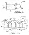
- a multi-beam antenna 10, 10.1comprises at least one electromagnetic lens 12 and a plurality of antenna feed elements 14 on a dielectric substrate 16 proximate to a first edge 18 thereof, wherein the plurality of antenna feed elements 14 are adapted to radiate a respective plurality of beams of electromagnetic energy 20 through the at least one electromagnetic lens 12.
- the at least one electromagnetic lens 12has a first side 22 having a first contour 24 at an intersection of the first side 22 with a reference surface 26, for example, a plane 26.1.
- the at least one electromagnetic lens 12acts to diffract the electromagnetic wave from the respective antenna feed elements 14, wherein different antenna feed elements 14 at different locations and in different directions relative to the at least one electromagnetic lens 12 generate different associated beams of electromagnetic energy 20.
- the at least one electromagnetic lens 12has a refractive index n different from free space, for example, a refractive index n greater than one (1).
- the at least one electromagnetic lens 12may be constructed of a material such as Rexolite TM , Teflon TM , polyethylene, or polystyrene; or a plurality of different materials having different refractive indices, for example as in a Luneburg lens.
- the shape and size of the at least one electromagnetic lens 12, the refractive index n thereof, and the relative position of the antenna feed elements 14 to the electromagnetic lens 12are adapted in accordance with the radiation patterns of the antenna feed elements 14 to provide a desired pattern of radiation of the respective beams of electromagnetic energy 20 exiting the second side 28 of the at least one electromagnetic lens 12.
- the at least one electromagnetic lens 12is illustrated as a spherical lens 12' in Figs. 1 and 2
- the at least one electromagnetic lens 12is not limited to any one particular design, and may, for example, comprise either a spherical lens, a Luneburg lens, a spherical shell lens, a hemispherical lens, an at least partially spherical lens, an at least partially spherical shell lens, a cylindrical lens, or a rotational lens.
- one or more portions of the electromagnetic lens 12may be truncated for improved packaging, without significantly impacting the performance of the associated multi-beam antenna 10,10.1.
- Fig. 3illustrates an at least partially spherical electromagnetic lens 12" with opposing first 27 and second 29 portions removed therefrom.
- the first edge 18 of the dielectric substrate 16comprises a second contour 30 that is proximate to the first contour 24.
- the first edge 18 of the dielectric substrate 16is located on the reference surface 26, and is positioned proximate to the first side 22 of one of the at least one electromagnetic lens 12.
- the dielectric substrate 16is located relative to the electromagnetic lens 12 so as to provide for the diffraction by the at least one electromagnetic lens 12 necessary to form the beams of electromagnetic energy 20.
- a multi-beam antenna 10comprising a planar dielectric substrate 16 located on reference surface 26 comprising a plane 26.1
- the plane 26.1may be located substantially close to the center 32 of the electromagnetic lens 12 so as to provide for diffraction by at least a portion of the electromagnetic lens 12.
- the dielectric substrate 16may also be displaced relative to the center 32 of the electromagnetic lens 12, for example on one or the other side of the center 32 as illustrated by dielectric substrates 16' and 16", which are located on respective reference surfaces 26' and 26".
- the dielectric substrate 16is, for example, a material with low loss at an operating frequency, for example, Duroid TM , a Teflon TM containing material, a ceramic material, or a composite material such as an epoxy/fiberglass composite.
- the dielectric substrate 16comprises a dielectric 16.1 of a circuit board 34, for example, a printed circuit board 34.1 comprising at least one conductive layer 36 adhered to dielectric substrate 16, from which the antenna feed elements 14 and other associated circuit traces 38 are formed, for example, by subtractive technology, for example, chemical or ion etching, or stamping; or additive techniques, for example, deposition, bonding or lamination.
- the plurality of antenna feed elements 14are located on the dielectric substrate 16 along the second contour 30 of the first edge 18, wherein each antenna feed element 14 comprises a least one conductor 40 operatively connected to the dielectric substrate 16.
- at least one of the antenna feed elements 14comprises an end-fire antenna element 14.1 adapted to launch or receive electromagnetic waves in a direction 42 substantially towards or from the first side 22 of the at least one electromagnetic lens 12, wherein different end-fire antenna elements 14.1 are located at different locations along the second contour 30 so as to launch or receive respective electromagnetic waves in different directions 42.
- An end-fire antenna element 14.1may, for example, comprise either a Yagi-Uda antenna, a coplanar horn antenna (also known as a tapered slot antenna), a Vivaldi antenna, a tapered dielectric rod, a slot antenna, a dipole antenna, or a helical antenna, each of which is capable of being formed on the dielectric substrate 16, for example, from a printed circuit board 34.1, for example, by subtractive technology, for example, chemical or ion etching, or stamping; or additive techniques, for example, deposition, bonding or lamination.
- the antenna feed elements 14may be used for transmitting, receiving or both.
- the direction 42 of the one or more beams of electromagnetic energy 20 through the electromagnetic lens 12, 12'is responsive to the relative location of the dielectric substrate 16, 16' or 16" and the associated reference surface 26, 26' or 26" relative to the center 32 of the electromagnetic lens 12.
- the directions 42 of the one or more beams of electromagnetic energy 20are nominally aligned with the reference surface 26.
- the resulting one or more beams of electromagnetic energy 20'propagate in directions 42' below the center 32.
- the resulting one or more beams of electromagnetic energy 20"propagate in directions 42" above the center 32.
- the multi-beam antenna 10may further comprise at least one transmission line 44 on the dielectric substrate 16 operatively connected to a feed port 46 of one of the plurality of antenna feed elements 14 for feeding a signal to the associated antenna feed element 14.
- the at least one transmission line 44may comprise either a stripline, a microstrip line, an inverted microstrip line, a slotline, an image line, an insulated image line, a tapped image line, a coplanar stripline, or a coplanar waveguide line formed on the dielectric substrate 16, for example, from a printed circuit board 34.1, for example, by subtractive technology, for example, chemical or ion etching, or stamping; or additive techniques, for example, deposition, bonding or lamination.
- the multi-beam antenna 10may further comprise a switching network 48 having at least one input 50 and a plurality of outputs 52, wherein the at least one input 50 is operatively connected -- for example, via at least one above described transmission line 44 -- to a corporate antenna feed port 54, and each output 52 of the plurality of outputs 52 is connected -- for example, via at least one above described transmission line 44 -- to a respective feed port 46 of a different antenna feed element 14 of the plurality of antenna feed elements 14.
- the switching network 48further comprises at least one control port 56 for controlling which outputs 52 are connected to the at least one input 50 at a given time.
- the switching network 48may, for example, comprise either a plurality of micro-mechanical switches, PIN diode switches, transistor switches, or a combination thereof, and may, for example, be operatively connected to the dielectric substrate 16, for example, by surface mount to an associated conductive layer 36 of a printed circuit board 34.1.
- a feed signal 58 applied to the corporate antenna feed port 54is either blocked -- for example, by an open circuit, by reflection or by absorption, -- or switched to the associated feed port 46 of one or more antenna feed elements 14, via one or more associated transmission lines 44, by the switching network 48, responsive to a control signal 60 applied to the control port 56.
- the feed signal 58may either comprise a single signal common to each antenna feed element 14, or a plurality of signals associated with different antenna feed elements 14.
- Each antenna feed element 14 to which the feed signal 58 is appliedlaunches an associated electromagnetic wave into the first side 22 of the associated electromagnetic lens 12, which is diffracted thereby to form an associated beam of electromagnetic energy 20.
- the associated beams of electromagnetic energy 20 launched by different antenna feed elements 14propagate in different associated directions 42.
- the various beams of electromagnetic energy 20may be generated individually at different times so as to provided for a scanned beam of electromagnetic energy 20. Alternately, two or more beams of electromagnetic energy 20 may be generated simultaneously.
- different antenna feed elements 14may be driven by different frequencies that, for example, are either directly switched to the respective antenna feed elements 14, or switched via an associated switching network 48 having a plurality of inputs 50, at least some of which are each connected to different feed signals 58.
- the multi-beam antenna 10, 10.1may be adapted so that the respective signals are associated with the respective antenna feed elements 14 in a one-to-one relationship, thereby precluding the need for an associated switching network 48.
- each antenna feed element 14can be operatively connected to an associated signal 59 through an associated processing element 61.
- the respective antenna feed elements 14are used to receive electromagnetic energy, and the respective processing elements 61 comprise detectors.
- the respective antenna feed elements 14are used to both transmit and receive electromagnetic energy, and the respective processing elements 61 comprise transmit/receive modules or transceivers.
- the switching network 48if used, need not be collocated on a common dielectric substrate 16, but can be separately located, as, for example, may be useful for low frequency applications, for example, 1-20 GHz.
- a multi-beam antenna 10'comprises at least a first 12.1 and a second 12.2 electromagnetic lens, each having a first side 22.1, 22.2 with a corresponding first contour 24.1, 24.2 at an intersection of the respective first side 22.1, 22.2 with the reference surface 26.
- the dielectric substrate 16comprises at least a second edge 62 comprising a third contour 64, wherein the second contour 30 is proximate to the first contour 24.1 of the first electromagnetic lens 12.1 and the third contour 64 is proximate to the first contour 24.2 of the second electromagnetic lens 12.2 .
- the second edge 62is the same as the first edge 18 and the second 30 and third 64 contours are displaced from one another along the first edge 18 of the dielectric substrate 16.
- the second edge 62is different from the first edge 18, and more particularly is opposite to the first edge 18 of the dielectric substrate 16.
- a multi-beam antenna 10"comprises at least one reflector 66, wherein the reference surface 26 intersects the at least one reflector 66 and one of the at least one electromagnetic lens 12 is located between the dielectric substrate 16 and the reflector 66.
- the at least one reflector 66is adapted to reflect electromagnetic energy propagated through the at least one electromagnetic lens 12 after being generated by at least one of the plurality of antenna feed elements 14.
- a third embodiment of the multi-beam antenna 10comprises at least first 66.1 and second 66.2 reflectors wherein the first electromagnetic lens 12.1 is located between the dielectric substrate 16 and the first reflector 66.1, the second electromagnetic lens 12.2 is located between the dielectric substrate 16 and the second reflector 66.2, the first reflector 66.1 is adapted to reflect electromagnetic energy propagated through the first electromagnetic lens 12.1 after being generated by at least one of the plurality of antenna feed elements 14 on the second contour 30, and the second reflector 66.2 is adapted to reflect electromagnetic energy propagated through the second electromagnetic lens 12.2 after being generated by at least one of the plurality of antenna feed elements 14 on the third contour 64.
- the first 66.1 and second 66.2 reflectorsmay be oriented to direct the beams of electromagnetic energy 20 from each side in a common nominal direction, as illustrated in Fig. 9 .
- the multi-beam antenna 10" as illustratedwould provide for scanning in a direction normal to the plane of the illustration. If the dielectric substrate 16 were rotated by 90 degrees with respect to the reflectors 66.1, 66.2, about an axis connecting the respective electromagnetic lenses 12.1, 12.1, then the multi-beam antenna 10" would provide for scanning in a direction parallel to the plane of the illustration.
- a multi-beam antenna 10", 10.4comprises an at least partially spherical electromagnetic lens 12"', for example, a hemispherical electromagnetic lens, having a curved surface 68 and a boundary 70, for example a flat boundary 70.1.
- the multi-beam antenna 10", 10.4further comprises a reflector 66 proximate to the boundary 70, and a plurality of antenna feed elements 14 on a dielectric substrate 16 proximate to a contoured edge 72 thereof, wherein each of the antenna feed elements 14 is adapted to radiate a respective plurality of beams of electromagnetic energy 20 into a first sector 74 of the electromagnetic lens 12"'.
- the electromagnetic lens 12"'has a first contour 24 at an intersection of the first sector 74 with a reference surface 26, for example, a plane 26.1.
- the contoured edge 72has a second contour 30 located on the reference surface 26 that is proximate to the first contour 24 of the first sector 74.
- the multi-beam antenna 10", 10.4further comprises a switching network 48 and a plurality of transmission lines 44 operatively connected to the antenna feed elements 14 as described hereinabove for the other embodiments.
- At least one feed signal 58 applied to a corporate antenna feed port 54is either blocked, or switched to the associated feed port 46 of one or more antenna feed elements 14, via one or more associated transmission lines 44, by the switching network 48 responsive to a control signal 60 applied to a control port 56 of the switching network 48.
- Each antenna feed element 14 to which the feed signal 58 is appliedlaunches an associated electromagnetic wave into the first sector 74 of the associated electromagnetic lens 12"'.
- the electromagnetic wavepropagates through -- and is diffracted by -- the curved surface 68, and is then reflected by the reflector 66 proximate to the boundary 70, whereafter the reflected electromagnetic wave propagates through the electromagnetic lens 12"' and exits -- and is diffracted by -- a second sector 76 as an associated beam of electromagnetic energy 20.
- the reflector 66substantially normal to the reference surface 26 -- as illustrated in Fig. 10 -- the different beams of electromagnetic energy 20 are directed by the associated antenna feed elements 14 in different directions that are nominally substantially parallel to the reference surface 26 .
- a multi-beam antenna 10"', 10.5comprises an electromagnetic lens 12 and plurality of dielectric substrates 16, each comprising a set of antenna feed elements 14 and operating in accordance with the description hereinabove.
- Each set of antenna feed elements 14generates (or is capable of generating) an associated set of beams of electromagnetic energy 20.1, 20.2 and 20.3, each having associated directions 42.1, 42.2 and 42.3, responsive to the associated feed 58 and control 60 signals.
- the associated feed 58 and control 60 signalsare either directly applied to the associated switch network 48 of the respective sets of antenna feed elements 14, or are applied thereto through a second switch network 78 have associated feed 80 and control 82 ports, each comprising at least one associated signal. Accordingly, the multi-beam antenna 10"', 10.4 provides for transmitting or receiving one or more beams of electromagnetic energy over a three-dimensional space.
- the multi-beam antenna 10provides for a relatively wide field-of-view, and is suitable for a variety of applications, including but not limited to automotive radar, point-to-point communications systems and point-to-multi-point communication systems, over a wide range of frequencies for which the antenna feed elements 14 may be designed to radiate, for example, 1 to 200 GHz. Moreover, the multi-beam antenna 10 may be configured for either mono-static or bi-static operation.
Landscapes
- Aerials With Secondary Devices (AREA)
- Variable-Direction Aerials And Aerial Arrays (AREA)
Description
- The instant invention generally relates to a multi-beam antenna comprising an electromagnetic lens and a plurality of antenna feed elements.
- Known waveguide based antennas, while relatively efficient, are bulky and relatively expensive to manufacture. Known phased array antennas are relatively compact but are relatively inefficient. Known focal plane antennas are compact but offer a comparatively narrow field of view.
US 5,583,511 discloses a stepped beam active array antenna comprising a feed array that includes a dielectric substrate and a plurality of radiating elements disposed on the substrate. In the disclosed embodiments, the radiating elements are disposed along a straight edge of the substrate which cooperate with a planar surface of an associated plano-convex lens. The focal plane of a disclosed transmit antenna embodiment is fully sampled. A stepped beam focal plane receive antenna is also disclosed.WO 92/13373 claim 1 is based, discloses a multi-beam antenna comprising a spherical dielectric lens and a plurality of helical antenna and associated feeder lines, wherein the helical antennas are integrated in the lens, and either fed in a backfire mode from inside the lens, or fed in an endfire mode outside the lens.- According to the present invention, there is provided a multi-beam antenna as defined in appended
claim 1. The antenna feed elements are operatively coupled to associated feed signals, which may be multiplexed through a switching network to a corporate antenna feed port. The multi-beam antenna may further comprise at least one reflector, wherein the at least one electromagnetic lens is located between the dielectric substrate and the at least one reflector, and the at least one reflector is adapted to reflect electromagnetic energy generated by at least one of the plurality of antenna feed elements and propagated through the at least one electromagnetic lens. - These and other objects, features, and advantages of the instant invention will be more fully understood after reading the following detailed description of the preferred embodiment with reference to the accompanying drawing.
- In the accompanying drawings:
FIG. 1 illustrates a top view of a first embodiment of a multi-beam antenna comprising an electromagnetic lens;FIG. 2 illustrates a side cross-section of the embodiment ofFig. 1 ;FIG. 3 illustrates a side cross-section of the embodiment ofFig. 1 incorporating a truncated electromagnetic lens;FIG. 4 illustrates a side cross-section of an embodiment illustrating various locations of a dielectric substrate, relative to an electromagnetic lens;FIG. 5 illustrates an embodiment wherein each antenna feed element is operatively coupled to a separate signal;FIG. 6 illustrates an embodiment wherein the switching network is separately located from the dielectric substrate;FIG. 7 illustrates a top view of a second embodiment of a multi-beam antenna, comprising a plurality electromagnetic lenses located proximate to one edge of a dielectric substrate;FIG. 8 illustrates a top view of a third embodiment of a multi-beam antenna, comprising a plurality electromagnetic lenses located proximate to opposite edges of a dielectric substrate;FIG. 9 illustrates a side view of the third embodiment illustrated inFig. 8 , further comprising a plurality of reflectors;FIG. 10 illustrates a fourth embodiment of a multi-beam antenna, comprising an electromagnetic lens and a reflector; andFIG. 11 illustrates a fifth embodiment of a multi-beam antenna.- Referring to
Figs. 1 and2 , amulti-beam antenna 10, 10.1 comprises at least oneelectromagnetic lens 12 and a plurality ofantenna feed elements 14 on adielectric substrate 16 proximate to afirst edge 18 thereof, wherein the plurality ofantenna feed elements 14 are adapted to radiate a respective plurality ofbeams ofelectromagnetic energy 20 through the at least oneelectromagnetic lens 12. - The at least one
electromagnetic lens 12 has afirst side 22 having afirst contour 24 at an intersection of thefirst side 22 with areference surface 26, for example, aplane 26.1. The at least oneelectromagnetic lens 12 acts to diffract the electromagnetic wave from the respectiveantenna feed elements 14, wherein differentantenna feed elements 14 at different locations and in different directions relative to the at least oneelectromagnetic lens 12 generate different associatedbeams ofelectromagnetic energy 20. The at least oneelectromagnetic lens 12 has arefractive index n different from free space, for example, arefractive index n greater than one (1). For example, the at least oneelectromagnetic lens 12 may be constructed of a material such as Rexolite™, Teflon™, polyethylene, or polystyrene; or a plurality of different materials having different refractive indices, for example as in a Luneburg lens. In accordance with known principles of diffraction, the shape and size of the at least oneelectromagnetic lens 12, therefractive index n thereof, and the relative position of theantenna feed elements 14 to theelectromagnetic lens 12 are adapted in accordance with the radiation patterns of theantenna feed elements 14 to provide a desired pattern of radiation of the respectivebeams ofelectromagnetic energy 20 exiting thesecond side 28 of the at least oneelectromagnetic lens 12. Whereas the at least oneelectromagnetic lens 12 is illustrated as aspherical lens 12' inFigs. 1 and2 , the at least oneelectromagnetic lens 12 is not limited to any one particular design, and may, for example, comprise either a spherical lens, a Luneburg lens, a spherical shell lens, a hemispherical lens, an at least partially spherical lens, an at least partially spherical shell lens, a cylindrical lens, or a rotational lens. Moreover, one or more portions of theelectromagnetic lens 12 may be truncated for improved packaging, without significantly impacting the performance of the associatedmulti-beam antenna 10,10.1. For example,Fig. 3 illustrates an at least partially sphericalelectromagnetic lens 12" with opposingfirst 27 andsecond 29 portions removed therefrom. - The
first edge 18 of thedielectric substrate 16 comprises asecond contour 30 that is proximate to thefirst contour 24. Thefirst edge 18 of thedielectric substrate 16 is located on thereference surface 26, and is positioned proximate to thefirst side 22 of one of the at least oneelectromagnetic lens 12. Thedielectric substrate 16 is located relative to theelectromagnetic lens 12 so as to provide for the diffraction by the at least oneelectromagnetic lens 12 necessary to form thebeams ofelectromagnetic energy 20. For the example of amulti-beam antenna 10 comprising a planardielectric substrate 16 located onreference surface 26 comprising aplane 26.1, in combination with anelectromagnetic lens 12 having acenter 32, for example, aspherical lens 12'; theplane 26.1 may be located substantially close to thecenter 32 of theelectromagnetic lens 12 so as to provide for diffraction by at least a portion of theelectromagnetic lens 12. Referring toFig. 4 , thedielectric substrate 16 may also be displaced relative to thecenter 32 of theelectromagnetic lens 12, for example on one or the other side of thecenter 32 as illustrated bydielectric substrates 16' and16", which are located onrespectivereference surfaces 26' and26". - The
dielectric substrate 16 is, for example, a material with low loss at an operating frequency, for example, Duroid™, a Teflon™ containing material, a ceramic material, or a composite material such as an epoxy/fiberglass composite. Moreover, in one embodiment, thedielectric substrate 16 comprises adielectric 16.1 of acircuit board 34, for example, aprinted circuit board 34.1 comprising at least oneconductive layer 36 adhered todielectric substrate 16, from which theantenna feed elements 14 and otherassociatedcircuit traces 38 are formed, for example, by subtractive technology, for example, chemical or ion etching, or stamping; or additive techniques, for example, deposition, bonding or lamination. - The plurality of
antenna feed elements 14 are located on thedielectric substrate 16 along thesecond contour 30 of thefirst edge 18, wherein eachantenna feed element 14 comprises a least oneconductor 40 operatively connected to thedielectric substrate 16. For example, at least one of theantenna feed elements 14 comprises anend-fire antenna element 14.1 adapted to launch or receive electromagnetic waves in adirection 42 substantially towards or from thefirst side 22 of the at least oneelectromagnetic lens 12, wherein differentend-fire antenna elements 14.1 are located at different locations along thesecond contour 30 so as to launch or receive respective electromagnetic waves indifferentdirections 42. Anend-fire antenna element 14.1 may, for example, comprise either a Yagi-Uda antenna, a coplanar horn antenna (also known as a tapered slot antenna), a Vivaldi antenna, a tapered dielectric rod, a slot antenna, a dipole antenna, or a helical antenna, each of which is capable of being formed on thedielectric substrate 16, for example, from aprinted circuit board 34.1, for example, by subtractive technology, for example, chemical or ion etching, or stamping; or additive techniques, for example, deposition, bonding or lamination. Moreover, theantenna feed elements 14 may be used for transmitting, receiving or both. - Referring to
Fig. 4 , thedirection 42 of the one or morebeams ofelectromagnetic energy 20 through theelectromagnetic lens 12, 12' is responsive to the relative location of thedielectric substrate reference surface center 32 of theelectromagnetic lens 12. For example, with thedielectric substrate 16 substantially aligned with thecenter 32, thedirections 42 of the one or morebeams ofelectromagnetic energy 20 are nominally aligned with thereference surface 26. Alternately, with thedielectric substrate 16' above thecenter 32 of theelectromagnetic lens 12, 12', the resulting one or morebeams of electromagnetic energy 20' propagate indirections 42' below thecenter 32. Similarly, with thedielectric substrate 16" below thecenter 32 of theelectromagnetic lens 12, 12', the resulting one or morebeams ofelectromagneticenergy 20" propagate indirections 42" above thecenter 32. - The
multi-beam antenna 10 may further comprise at least onetransmission line 44 on thedielectric substrate 16 operatively connected to afeed port 46 of one of the plurality ofantenna feed elements 14 for feeding a signal to the associatedantenna feed element 14. For example, the at least onetransmission line 44 may comprise either a stripline, a microstrip line, an inverted microstrip line, a slotline, an image line, an insulated image line, a tapped image line, a coplanar stripline, or a coplanar waveguide line formed on thedielectric substrate 16, for example, from aprinted circuit board 34.1, for example, by subtractive technology, for example, chemical or ion etching, or stamping; or additive techniques, for example, deposition, bonding or lamination. - The
multi-beam antenna 10 may further comprise aswitching network 48 having at least oneinput 50 and a plurality ofoutputs 52, wherein the at least oneinput 50 is operatively connected -- for example, via at least one above describedtransmission line 44 -- to acorporateantenna feed port 54, and eachoutput 52 of the plurality ofoutputs 52 is connected -- for example, via at least one above describedtransmission line 44 -- to arespectivefeed port 46 of a differentantenna feed element 14 of the plurality ofantenna feed elements 14. Theswitching network 48 further comprises at least onecontrol port 56 for controlling whichoutputs 52 are connected to the at least oneinput 50 at a given time. Theswitching network 48 may, for example, comprise either a plurality of micro-mechanical switches, PIN diode switches, transistor switches, or a combination thereof, and may, for example, be operatively connected to thedielectric substrate 16, for example, by surface mount to an associatedconductive layer 36 of aprinted circuit board 34.1. - In operation, a
feed signal 58 applied to thecorporateantenna feed port 54 is either blocked -- for example, by an open circuit, by reflection or by absorption, -- or switched to the associatedfeed port 46 of one or moreantenna feed elements 14, via one or more associatedtransmission lines 44, by theswitching network 48, responsive to acontrol signal 60 applied to thecontrol port 56. It should be understood that thefeed signal 58 may either comprise a single signal common to eachantenna feed element 14, or a plurality of signals associated with differentantenna feed elements 14. Eachantenna feed element 14 to whichthefeed signal 58 is applied launches an associated electromagnetic wave into thefirst side 22 of the associatedelectromagnetic lens 12, which is diffracted thereby to form an associatedbeam ofelectromagnetic energy 20. The associatedbeams ofelectromagnetic energy 20 launched by differentantenna feed elements 14 propagate in different associateddirections 42. The variousbeams ofelectromagnetic energy 20 may be generated individually at different times so as to provided for a scannedbeam ofelectromagnetic energy 20. Alternately, two or morebeams ofelectromagnetic energy 20 may be generated simultaneously. Moreover, differentantenna feed elements 14 may be driven by different frequencies that, for example, are either directly switched to the respectiveantenna feed elements 14, or switched via an associatedswitching network 48 having a plurality ofinputs 50, at least some of which are each connected to differentfeed signals 58. - Referring to
Fig. 5 , themulti-beam antenna 10, 10.1 may be adapted so that the respective signals are associated with the respectiveantenna feed elements 14 in a one-to-one relationship, thereby precluding the need for an associatedswitching network 48. For example, eachantenna feed element 14 can be operatively connected to an associatedsignal 59 through an associatedprocessing element 61. As one example, with themulti-beam antenna 10, 10.1 configured as an imaging array, the respectiveantenna feed elements 14 are used to receive electromagnetic energy, and therespectiveprocessing elements 61 comprise detectors. As another example, with themulti-beam antenna 10, 10.1 configured as a communication antenna, the respectiveantenna feed elements 14 are used to both transmit and receive electromagnetic energy, and therespectiveprocessing elements 61 comprise transmit/receive modules or transceivers. - Referring to
Fig. 6 , theswitchingnetwork 48, if used, need not be collocated on acommondielectric substrate 16, but can be separately located, as, for example, may be useful for low frequency applications, for example, 1-20 GHz. - Referring to
Figs. 7 ,8 and9 , in accordance with a second aspect, amulti-beam antenna 10' comprises at least afirst 12.1 and asecond 12.2 electromagnetic lens, each having afirst side 22.1, 22.2 with a correspondingfirst contour 24.1, 24.2 at an intersection of the respectivefirst side 22.1, 22.2 with thereference surface 26. Thedielectric substrate 16 comprises at least asecond edge 62 comprisingathird contour 64, wherein thesecond contour 30 is proximate to thefirst contour 24.1 of thefirst electromagnetic lens 12.1 and thethird contour 64 is proximate to thefirst contour 24.2 of the secondelectromagnetic lens 12.2. - Referring to
Fig. 7 , in accordance with a second embodiment of themulti-beam antenna 10.2, thesecond edge 62 is the same as thefirst edge 18 and thesecond 30 andthird 64 contours are displaced from one another along thefirst edge 18 of thedielectric substrate 16. - Referring to
Fig. 8 , in accordance with a third embodiment of themulti-beam antenna 10.3, thesecond edge 62 is different from thefirst edge 18, and more particularly is opposite to thefirst edge 18 of thedielectric substrate 16. - Referring to
Fig. 9 , in accordance with a third aspect, amulti-beam antenna 10" comprises at least onereflector 66, wherein thereference surface 26 intersects the at least onereflector 66 and one of the at least oneelectromagnetic lens 12 is located between thedielectric substrate 16 and thereflector 66. The at least onereflector 66 is adapted to reflect electromagnetic energy propagated through the at least oneelectromagnetic lens 12 after being generated by at least one of the plurality ofantenna feed elements 14. A third embodiment of themulti-beam antenna 10 comprises at leastfirst 66.1 andsecond 66.2 reflectors wherein thefirst electromagnetic lens 12.1 is located between thedielectric substrate 16 and thefirst reflector 66.1, thesecond electromagnetic lens 12.2 is located between thedielectric substrate 16 and thesecond reflector 66.2, thefirst reflector 66.1 is adapted to reflect electromagnetic energy propagated through thefirst electromagnetic lens 12.1 after being generated by at least one of the plurality ofantenna feed elements 14 on thesecond contour 30, and thesecond reflector 66.2 is adapted to reflect electromagnetic energy propagated through thesecond electromagnetic lens 12.2 after being generated by at least one of the plurality ofantenna feed elements 14 on thethird contour 64. For example, thefirst 66.1 andsecond 66.2 reflectors may be oriented to direct thebeams ofelectromagnetic energy 20 from each side in a common nominal direction, as illustrated inFig. 9 . Referring toFig. 9 , themulti-beam antenna 10" as illustrated would provide for scanning in a direction normal to the plane of the illustration. If thedielectric substrate 16 were rotated by90 degrees with respect to thereflectors 66.1, 66.2, about an axis connecting the respectiveelectromagnetic lenses 12.1, 12.1, then themulti-beam antenna 10" would provide for scanning in a direction parallel to the plane of the illustration. - Referring to
Fig. 10 , in accordance with the third aspect and a fourth embodiment, amulti-beam antenna 10", 10.4 comprises an at least partially sphericalelectromagnetic lens 12"', for example, a hemispherical electromagnetic lens, having acurved surface 68 and aboundary 70, for example aflat boundary 70.1. Themulti-beam antenna 10", 10.4 further comprises areflector 66 proximate to theboundary 70, and a plurality ofantenna feed elements 14 on adielectric substrate 16 proximate to acontourededge 72 thereof, wherein each of theantenna feed elements 14 is adapted to radiate a respective plurality ofbeams ofelectromagnetic energy 20 into afirst sector 74 of theelectromagnetic lens 12"'. Theelectromagnetic lens 12"' has afirst contour 24 at an intersection of thefirst sector 74 with areference surface 26, for example, aplane 26.1. Thecontourededge 72 has asecond contour 30 located on thereference surface 26 that is proximate to thefirst contour 24 of thefirst sector 74. Themulti-beam antenna 10", 10.4 further comprises aswitching network 48 and a plurality oftransmission lines 44 operatively connected to theantenna feed elements 14 as described hereinabove for the other embodiments. - In operation, at least one
feed signal 58 applied to acorporateantenna feed port 54 is either blocked, or switched to the associatedfeed port 46 of one or moreantenna feed elements 14, via one or more associatedtransmission lines 44, by theswitchingnetwork 48 responsive to acontrol signal 60 applied to acontrol port 56 of theswitching network 48. Eachantenna feed element 14 to which thefeed signal 58 is applied launches an associated electromagnetic wave into thefirst sector 74 of the associatedelectromagnetic lens 12"'. The electromagnetic wave propagates through -- and is diffracted by -- thecurved surface 68, and is then reflected by thereflector 66 proximate to theboundary 70, whereafter the reflected electromagnetic wave propagates through theelectromagnetic lens 12"' and exits -- and is diffracted by -- asecond sector 76 as an associatedbeam ofelectromagnetic energy 20. With thereflector 66 substantially normal to thereference surface 26 -- as illustrated inFig. 10 -- the differentbeams ofelectromagnetic energy 20 are directed by the associatedantenna feed elements 14 in different directions that are nominally substantially parallel to thereference surface 26. - Referring to
Fig. 11 , in accordance with a fourth aspect and a fifth embodiment, amulti-beam antenna 10"', 10.5 comprises anelectromagnetic lens 12 and plurality ofdielectric substrates 16, each comprising a set ofantenna feed elements 14 and operating in accordance with the description hereinabove. Each set ofantenna feed elements 14 generates (or is capable of generating) an associated set ofbeams of electromagnetic energy 20.1, 20.2 and20.3, each having associateddirections 42.1, 42.2 and42.3, responsive to the associatedfeed 58 andcontrol 60 signals. The associatedfeed 58 andcontrol 60 signals are either directly applied to the associatedswitch network 48 of the respective sets ofantenna feed elements 14, or are applied thereto through asecond switch network 78 have associatedfeed 80 andcontrol 82 ports, each comprising at least one associated signal. Accordingly, themulti-beam antenna 10"', 10.4 provides for transmitting or receiving one or more beams of electromagnetic energy over a three-dimensional space. - The
multi-beam antenna 10 provides for a relatively wide field-of-view, and is suitable for a variety of applications, including but not limited to automotive radar, point-to-point communications systems and point-to-multi-point communication systems, over a wide range of frequencies for which theantenna feed elements 14 may be designed to radiate, for example,1 to 200GHz. Moreover, themulti-beam antenna 10 may be configured for either mono-static or bi-static operation. - While specific embodiments have been described in detail in the foregoing detailed description and illustrated in the accompanying drawings, those with ordinary skill in the art will appreciate that various modifications and alternatives to those details could be developed in light of the overall teachings of the disclosure. Accordingly, the particular arrangements disclosed are meant to be illustrative only and not limiting as to the scope of the invention, which is to be given the full breadth of the appended claims and any and all equivalents thereof.
Claims (10)
- A multi-beam antenna (10), comprising,a. at least one electromagnetic lens (12), wherein said at least one electromagnetic lens (12) has a first side (22) comprising a first contour (24); andb. for said at least one electromagnetic lens (12), a plurality of antenna feed elements (14), wherein at least one said antenna feed element (14) comprises an end-fire antenna element (14.1) adapted to launch electromagnetic waves (20) in a direction (42) substantially towards said first side (22) of said at least one electromagnetic lens (12), and said direction (42) for at least one said end-fire antenna element (14.1) is different from said direction (42) for at least another said end-fire antenna element (14.1);characterized by further comprisingc. a dielectric substrate (16) located on a reference surface (26), wherein said dielectric substrate (16) comprises a first edge (18) comprising a second contour (30) proximate to said first contour (24), said first edge (18) of said dielectric substrate (16) is located on said reference surface (26), said first contour (24) is at an intersection of said reference surface (26) with said first side (22) of said at least one electromagnetic lens (12), said first edge (18) is proximate to said first side (22) of said at least one electromagnetic lens (12), and said plurality of antenna feed elements (14) are formed from a conductive layer on said dielectric substrate (16) and located at different locations along said second contour (30) of said first edge (18).
- A multi-beam antenna (10) as recited in claim 1, wherein each said antenna feed element (14) comprises a least one conductor (40) operatively connected to said dielectric substrate (16).
- A multi-beam antenna (10) as recited in any of claims 1 or 2, further comprising at least one transmission line (44) on said dielectric substrate (16), wherein at least one said at least one transmission line (44) is operatively connected to a feed port (46) of one of said plurality of antenna feed elements (14).
- A multi-beam antenna (10) as recited in any of claims 1 through 3, further comprising a switching network (48) having an input (50) and a plurality of outputs (52), said input (50) is operatively connected to a corporate antenna feed port (54), and each output (52) of said plurality of outputs (52) is connected to a different antenna feed element (14) of said plurality of antenna feed elements (14).
- A multi-beam antenna (10, 10', 10.2, 10.3) as recited in any of claims 1 through 4, wherein said at least one electromagnetic lens (12) comprises at least a first (12.1) and a second (12.2) electromagnetic lens, each of said first (12.1) and second (12.2) electromagnetic lenses has a first side (22.1, 22.2), each said first side (22.1, 22.2) has a corresponding first contour (24.1, 24.2) at an intersection of said first side (22.1, 22.2) with said reference surface (26), said dielectric substrate (16) comprises at least a second edge (62), said second edge (62) comprises a third contour (64), said second contour (30) is proximate to said first contour (24.1) of said first electromagnetic lens (12.1), said third contour (64) is proximate to said first contour (24.2) of said second electromagnetic lens (12.2), further comprising at least one antenna feed element (14) on said dielectric substrate (16) along said third contour (64) of said second edge (62).
- A multi-beam antenna (10, 10', 10.2) as recited in claim 5, wherein said second edge (62) is the same as said first edge (18) and said second (30) and third (64) contours are displaced from one another along said first edge (18).
- A multi-beam antenna (10, 10', 10.2, 10.3) as recited in claim 5, wherein said second edge (62) is different from said first edge (18).
- A multi-beam antenna (10, 10', 10.3) as recited in either of claims 5 or 7, wherein said second edge (62) is opposite to said first edge (18).
- A multi-beam antenna (10, 10', 10", 10.3) as recited in any of claims 1 through 8, further comprising at least one reflector (66, 66.1, 66.2), wherein said reference surface (26) intersects said at least one reflector (66, 66.1, 66.2), one of said at least one electromagnetic lens (12, 12.1, 12.2) is located between said dielectric substrate (16) and said reflector (66, 66.1, 66.2), and said at least one reflector (66, 66.1, 66.2) is adapted to reflect electromagnetic energy (20) propagated through said at least one electromagnetic lens (12, 12.1, 12.2) after being generated by at least one of said plurality of antenna feed elements (14).
- A multi-beam antenna (10, 10', 10", 10.3) as recited in any of claims 5 through 8, further comprising at least first (66.1) and second (66.2) reflectors wherein said reference surface (26) intersects said at least first (66.1) and second (66.2) reflectors, said first electromagnetic lens (12.1) is located between said dielectric substrate (16) and said first reflector (66.1), said second electromagnetic lens (12.2) is located between said dielectric substrate (16) and said second reflector (66.2), said first reflector (66.1) is adapted to reflect electromagnetic energy (20) propagated through said first electromagnetic lens (12.1) after being generated by at least one of said plurality of antenna feed elements (14) on said second contour (30), and said second reflector (66.2) is adapted to reflect electromagnetic energy (20) propagated through said second electromagnetic lens (12.2) after being generated by said at least one antenna feed element (14) on said third contour (64).
Priority Applications (1)
| Application Number | Priority Date | Filing Date | Title |
|---|---|---|---|
| EP06024287AEP1764868A1 (en) | 1999-11-18 | 2000-11-20 | Multi-beam antenna |
Applications Claiming Priority (3)
| Application Number | Priority Date | Filing Date | Title |
|---|---|---|---|
| US16623199P | 1999-11-18 | 1999-11-18 | |
| US166231P | 1999-11-18 | ||
| PCT/US2000/031858WO2001037374A1 (en) | 1999-11-18 | 2000-11-20 | Multi-beam antenna |
Related Child Applications (1)
| Application Number | Title | Priority Date | Filing Date |
|---|---|---|---|
| EP06024287ADivisionEP1764868A1 (en) | 1999-11-18 | 2000-11-20 | Multi-beam antenna |
Publications (3)
| Publication Number | Publication Date |
|---|---|
| EP1236245A1 EP1236245A1 (en) | 2002-09-04 |
| EP1236245A4 EP1236245A4 (en) | 2004-08-18 |
| EP1236245B1true EP1236245B1 (en) | 2008-05-28 |
Family
ID=22602373
Family Applications (1)
| Application Number | Title | Priority Date | Filing Date |
|---|---|---|---|
| EP00980567AExpired - LifetimeEP1236245B1 (en) | 1999-11-18 | 2000-11-20 | Multi-beam antenna |
Country Status (5)
| Country | Link |
|---|---|
| US (1) | US6424319B2 (en) |
| EP (1) | EP1236245B1 (en) |
| JP (1) | JP2003514477A (en) |
| DE (1) | DE60039065D1 (en) |
| WO (1) | WO2001037374A1 (en) |
Families Citing this family (56)
| Publication number | Priority date | Publication date | Assignee | Title |
|---|---|---|---|---|
| US7358913B2 (en)* | 1999-11-18 | 2008-04-15 | Automotive Systems Laboratory, Inc. | Multi-beam antenna |
| US7994996B2 (en)* | 1999-11-18 | 2011-08-09 | TK Holding Inc., Electronics | Multi-beam antenna |
| US6606077B2 (en)* | 1999-11-18 | 2003-08-12 | Automotive Systems Laboratory, Inc. | Multi-beam antenna |
| US7042420B2 (en)* | 1999-11-18 | 2006-05-09 | Automotive Systems Laboratory, Inc. | Multi-beam antenna |
| US20050219126A1 (en)* | 2004-03-26 | 2005-10-06 | Automotive Systems Laboratory, Inc. | Multi-beam antenna |
| US6661392B2 (en)* | 2001-08-17 | 2003-12-09 | Lucent Technologies Inc. | Resonant antennas |
| DE10205379A1 (en)* | 2002-02-09 | 2003-08-21 | Bosch Gmbh Robert | Device for transmitting and receiving electromagnetic radiation |
| US7276990B2 (en) | 2002-05-15 | 2007-10-02 | Hrl Laboratories, Llc | Single-pole multi-throw switch having low parasitic reactance, and an antenna incorporating the same |
| US7298228B2 (en)* | 2002-05-15 | 2007-11-20 | Hrl Laboratories, Llc | Single-pole multi-throw switch having low parasitic reactance, and an antenna incorporating the same |
| WO2004040694A1 (en)* | 2002-10-24 | 2004-05-13 | Centre National De La Recherche Scientifique (C.N.R.S.) | Multiple-beam antenna with photonic bandgap material |
| JP4513797B2 (en)* | 2003-04-02 | 2010-07-28 | 住友電気工業株式会社 | Radio wave lens antenna device |
| DE602004015955D1 (en)* | 2003-04-02 | 2008-10-02 | Sumitomo Electric Industries | RADIO WAVES LENS ANTENNA DEVICE |
| US7456803B1 (en) | 2003-05-12 | 2008-11-25 | Hrl Laboratories, Llc | Large aperture rectenna based on planar lens structures |
| US7253699B2 (en) | 2003-05-12 | 2007-08-07 | Hrl Laboratories, Llc | RF MEMS switch with integrated impedance matching structure |
| US7245269B2 (en) | 2003-05-12 | 2007-07-17 | Hrl Laboratories, Llc | Adaptive beam forming antenna system using a tunable impedance surface |
| US7071888B2 (en) | 2003-05-12 | 2006-07-04 | Hrl Laboratories, Llc | Steerable leaky wave antenna capable of both forward and backward radiation |
| US7154451B1 (en) | 2004-09-17 | 2006-12-26 | Hrl Laboratories, Llc | Large aperture rectenna based on planar lens structures |
| US7068234B2 (en) | 2003-05-12 | 2006-06-27 | Hrl Laboratories, Llc | Meta-element antenna and array |
| US7164387B2 (en)* | 2003-05-12 | 2007-01-16 | Hrl Laboratories, Llc | Compact tunable antenna |
| JP3867713B2 (en)* | 2003-06-05 | 2007-01-10 | 住友電気工業株式会社 | Radio wave lens antenna device |
| US7015865B2 (en)* | 2004-03-10 | 2006-03-21 | Lucent Technologies Inc. | Media with controllable refractive properties |
| GB0406814D0 (en)* | 2004-03-26 | 2004-08-04 | Bae Systems Plc | An antenna |
| JP2008503904A (en)* | 2004-03-26 | 2008-02-07 | オートモーティブ システムズ ラボラトリー インコーポレーテッド | Multi-beam antenna |
| US7009565B2 (en)* | 2004-07-30 | 2006-03-07 | Lucent Technologies Inc. | Miniaturized antennas based on negative permittivity materials |
| JP2008510390A (en)* | 2004-08-11 | 2008-04-03 | オートモーティブ システムズ ラボラトリー インコーポレーテッド | Multi-beam antenna |
| US7580004B1 (en)* | 2005-01-25 | 2009-08-25 | Location & Tracking Technologies, Llc | System and method for position or range estimation, tracking and selective interrogation and communication |
| JP2008530914A (en)* | 2005-02-10 | 2008-08-07 | オートモーティブ システムズ ラボラトリー インコーポレーテッド | Vehicle radar system with guard beam |
| WO2006122040A2 (en)* | 2005-05-05 | 2006-11-16 | Automotive Systems Laboratory, Inc. | Antenna |
| US7573369B2 (en)* | 2005-09-07 | 2009-08-11 | Atr Electronics, Inc. | System and method for interrogating and locating a transponder relative to a zone-of-interest |
| JP4816078B2 (en)* | 2005-12-28 | 2011-11-16 | 住友電気工業株式会社 | Radio wave lens antenna device |
| US7307589B1 (en) | 2005-12-29 | 2007-12-11 | Hrl Laboratories, Llc | Large-scale adaptive surface sensor arrays |
| US7420525B2 (en)* | 2006-06-23 | 2008-09-02 | Gm Global Technology Operations, Inc. | Multi-beam antenna with shared dielectric lens |
| FR2925772A1 (en)* | 2007-12-21 | 2009-06-26 | Thomson Licensing Sas | RADIANT MULTI-SECTOR DEVICE HAVING AN OMNIDIRECTIONAL MODE |
| US7868829B1 (en) | 2008-03-21 | 2011-01-11 | Hrl Laboratories, Llc | Reflectarray |
| DE102008001467A1 (en)* | 2008-04-30 | 2009-11-05 | Robert Bosch Gmbh | Multibeam radar sensor |
| US8994609B2 (en) | 2011-09-23 | 2015-03-31 | Hrl Laboratories, Llc | Conformal surface wave feed |
| US8436785B1 (en) | 2010-11-03 | 2013-05-07 | Hrl Laboratories, Llc | Electrically tunable surface impedance structure with suppressed backward wave |
| US9466887B2 (en) | 2010-11-03 | 2016-10-11 | Hrl Laboratories, Llc | Low cost, 2D, electronically-steerable, artificial-impedance-surface antenna |
| EP2523256B1 (en) | 2011-05-13 | 2013-07-24 | Thomson Licensing | Multibeam antenna system |
| GB2492081B (en) | 2011-06-20 | 2014-11-19 | Canon Kk | Antenna lens including holes and different permittivity layers |
| US8982011B1 (en) | 2011-09-23 | 2015-03-17 | Hrl Laboratories, Llc | Conformal antennas for mitigation of structural blockage |
| CN102610926A (en)* | 2012-04-11 | 2012-07-25 | 哈尔滨工业大学 | Dielectric lens antenna for high-altitude platform communication system |
| CN102800951A (en)* | 2012-08-06 | 2012-11-28 | 哈尔滨工业大学 | Printed Yagi antenna of vibrator loading type balance microstrip line feed |
| WO2016057115A1 (en) | 2014-10-09 | 2016-04-14 | Utc Fire & Security Corporation | Device for providing wireless energy transfer |
| CN113140915A (en)* | 2016-03-25 | 2021-07-20 | 康普技术有限责任公司 | Antenna with lens formed of lightweight dielectric material and associated dielectric material |
| US11431100B2 (en) | 2016-03-25 | 2022-08-30 | Commscope Technologies Llc | Antennas having lenses formed of lightweight dielectric materials and related dielectric materials |
| WO2017173208A1 (en)* | 2016-03-31 | 2017-10-05 | Commscope Technologies Llc | Lensed antennas for use in wireless communications systems |
| EP3242358B1 (en) | 2016-05-06 | 2020-06-17 | Amphenol Antenna Solutions, Inc. | High gain, multi-beam antenna for 5g wireless communications |
| EP3616265A4 (en)* | 2017-04-24 | 2021-01-13 | Cohere Technologies, Inc. | Multibeam antenna designs and operation |
| CN111095674B (en) | 2017-09-15 | 2022-02-18 | 康普技术有限责任公司 | Method for preparing composite dielectric material |
| US11532891B2 (en)* | 2017-09-20 | 2022-12-20 | Cohere Technologies, Inc. | Low cost electromagnetic feed network |
| EP3648251A1 (en)* | 2018-10-29 | 2020-05-06 | AT & S Austria Technologie & Systemtechnik Aktiengesellschaft | Integration of all components being necessary for transmitting / receiving electromagnetic radiation in a component carrier |
| US11843170B2 (en)* | 2019-03-15 | 2023-12-12 | John Mezzalingua Associates, LLC | Spherical Luneburg lens-enhanced compact multi-beam antenna |
| JP2019213222A (en)* | 2019-09-05 | 2019-12-12 | パナソニックIpマネジメント株式会社 | vehicle |
| CN110957573B (en)* | 2019-11-25 | 2022-03-29 | 北京军懋国兴科技股份有限公司 | Dual-band airborne composite antenna |
| CN114759367B (en)* | 2022-06-14 | 2022-10-04 | 西安海天天线科技股份有限公司 | Multi-frequency artificial medium multi-beam lens antenna and use method |
Family Cites Families (24)
| Publication number | Priority date | Publication date | Assignee | Title |
|---|---|---|---|---|
| US3761936A (en)* | 1971-05-11 | 1973-09-25 | Raytheon Co | Multi-beam array antenna |
| US4222054A (en)* | 1978-10-30 | 1980-09-09 | Raytheon Company | Radio frequency lens |
| US4268831A (en)* | 1979-04-30 | 1981-05-19 | Sperry Corporation | Antenna for scanning a limited spatial sector |
| US4288795A (en)* | 1979-10-25 | 1981-09-08 | The United States Of America As Represented By The Secretary Of The Navy | Anastigmatic three-dimensional bootlace lens |
| JPS60170304A (en)* | 1984-02-15 | 1985-09-03 | Toshiba Corp | Antenna system |
| US4641144A (en)* | 1984-12-31 | 1987-02-03 | Raytheon Company | Broad beamwidth lens feed |
| US4845507A (en)* | 1987-08-07 | 1989-07-04 | Raytheon Company | Modular multibeam radio frequency array antenna system |
| US4983237A (en)* | 1988-08-18 | 1991-01-08 | Hughes Aircraft Company | Antenna lamination technique |
| US5099253A (en)* | 1989-11-06 | 1992-03-24 | Raytheon Company | Constant beamwidth scanning array |
| US5274389A (en)* | 1990-06-21 | 1993-12-28 | Raytheon Company | Broadband direction finding system |
| US5206658A (en)* | 1990-10-31 | 1993-04-27 | Rockwell International Corporation | Multiple beam antenna system |
| WO1992013373A1 (en)* | 1991-01-28 | 1992-08-06 | Thomson Consumer Electronics S.A. | Antenna system |
| US5347287A (en)* | 1991-04-19 | 1994-09-13 | Hughes Missile Systems Company | Conformal phased array antenna |
| US5892487A (en)* | 1993-02-28 | 1999-04-06 | Thomson Multimedia S.A. | Antenna system |
| CA2147399A1 (en)* | 1994-06-01 | 1995-12-02 | Noach Amitay | Feed structure for use in a wireless communication system |
| US5583511A (en)* | 1995-06-06 | 1996-12-10 | Hughes Missile Systems Company | Stepped beam active array antenna and radar system employing same |
| FR2738954B1 (en) | 1995-09-19 | 1997-11-07 | Dassault Electronique | IMPROVED ELECTRONIC SCANNING ANTENNA |
| US5712643A (en)* | 1995-12-05 | 1998-01-27 | Cushcraft Corporation | Planar microstrip Yagi Antenna array |
| US5821908A (en)* | 1996-03-22 | 1998-10-13 | Ball Aerospace And Technologies Corp. | Spherical lens antenna having an electronically steerable beam |
| US6031501A (en)* | 1997-03-19 | 2000-02-29 | Georgia Tech Research Corporation | Low cost compact electronically scanned millimeter wave lens and method |
| US6061035A (en) | 1997-04-02 | 2000-05-09 | The United States Of America As Represented By The Secretary Of The Army | Frequency-scanned end-fire phased-aray antenna |
| US5894288A (en)* | 1997-08-08 | 1999-04-13 | Raytheon Company | Wideband end-fire array |
| US5874915A (en)* | 1997-08-08 | 1999-02-23 | Raytheon Company | Wideband cylindrical UHF array |
| US6046703A (en) | 1998-11-10 | 2000-04-04 | Nutex Communication Corp. | Compact wireless transceiver board with directional printed circuit antenna |
- 2000
- 2000-11-20DEDE60039065Tpatent/DE60039065D1/ennot_activeExpired - Fee Related
- 2000-11-20JPJP2001537823Apatent/JP2003514477A/enactivePending
- 2000-11-20EPEP00980567Apatent/EP1236245B1/ennot_activeExpired - Lifetime
- 2000-11-20WOPCT/US2000/031858patent/WO2001037374A1/enactiveApplication Filing
- 2000-11-20USUS09/716,736patent/US6424319B2/ennot_activeExpired - Lifetime
Also Published As
| Publication number | Publication date |
|---|---|
| DE60039065D1 (en) | 2008-07-10 |
| EP1236245A1 (en) | 2002-09-04 |
| JP2003514477A (en) | 2003-04-15 |
| US6424319B2 (en) | 2002-07-23 |
| US20020003505A1 (en) | 2002-01-10 |
| EP1236245A4 (en) | 2004-08-18 |
| WO2001037374A1 (en) | 2001-05-25 |
Similar Documents
| Publication | Publication Date | Title |
|---|---|---|
| EP1236245B1 (en) | Multi-beam antenna | |
| US6606077B2 (en) | Multi-beam antenna | |
| US7042420B2 (en) | Multi-beam antenna | |
| US7358913B2 (en) | Multi-beam antenna | |
| US7898480B2 (en) | Antenna | |
| US7605768B2 (en) | Multi-beam antenna | |
| US8284102B2 (en) | Displaced feed parallel plate antenna | |
| WO2008061107A2 (en) | Antenna | |
| JP3534410B2 (en) | Radiation sensor | |
| EP1886383A2 (en) | Antenna | |
| CN110571530A (en) | A Reconfigurable Parabolic Antenna with Integrated Reflect Array | |
| EP1764868A1 (en) | Multi-beam antenna | |
| WO2004038452A1 (en) | Adaptive antenna | |
| EP1779465A2 (en) | Multi-beam antenna | |
| Tuloti et al. | A Highly Compact Low-Profile Beam Switching Transmitarray Antenna for ISM-Band Applications | |
| EP1647070B1 (en) | An antenna | |
| CN111211404B (en) | Low-profile scannable planar reflective array antenna system with rotary sub-reflecting surface and scanning method | |
| US5995056A (en) | Wide band tem fed phased array reflector antenna | |
| CN117199830A (en) | Multi-beam antenna module |
Legal Events
| Date | Code | Title | Description |
|---|---|---|---|
| PUAI | Public reference made under article 153(3) epc to a published international application that has entered the european phase | Free format text:ORIGINAL CODE: 0009012 | |
| 17P | Request for examination filed | Effective date:20020521 | |
| AK | Designated contracting states | Kind code of ref document:A1 Designated state(s):AT BE CH CY DE DK ES FI FR GB GR IE IT LI LU MC NL PT SE TR | |
| AX | Request for extension of the european patent | Free format text:AL;LT;LV;MK;RO;SI | |
| RBV | Designated contracting states (corrected) | Designated state(s):AT BE CH CY DE FR GB LI SE | |
| A4 | Supplementary search report drawn up and despatched | Effective date:20040701 | |
| RIC1 | Information provided on ipc code assigned before grant | Ipc:7H 01Q 13/08 B Ipc:7H 01Q 25/00 A | |
| 17Q | First examination report despatched | Effective date:20041025 | |
| GRAP | Despatch of communication of intention to grant a patent | Free format text:ORIGINAL CODE: EPIDOSNIGR1 | |
| RBV | Designated contracting states (corrected) | Designated state(s):DE FR GB SE | |
| GRAS | Grant fee paid | Free format text:ORIGINAL CODE: EPIDOSNIGR3 | |
| 17Q | First examination report despatched | Effective date:20041025 | |
| GRAA | (expected) grant | Free format text:ORIGINAL CODE: 0009210 | |
| AK | Designated contracting states | Kind code of ref document:B1 Designated state(s):DE FR GB SE | |
| REG | Reference to a national code | Ref country code:GB Ref legal event code:FG4D | |
| REF | Corresponds to: | Ref document number:60039065 Country of ref document:DE Date of ref document:20080710 Kind code of ref document:P | |
| PG25 | Lapsed in a contracting state [announced via postgrant information from national office to epo] | Ref country code:SE Free format text:LAPSE BECAUSE OF FAILURE TO SUBMIT A TRANSLATION OF THE DESCRIPTION OR TO PAY THE FEE WITHIN THE PRESCRIBED TIME-LIMIT Effective date:20080828 | |
| PLBE | No opposition filed within time limit | Free format text:ORIGINAL CODE: 0009261 | |
| STAA | Information on the status of an ep patent application or granted ep patent | Free format text:STATUS: NO OPPOSITION FILED WITHIN TIME LIMIT | |
| 26N | No opposition filed | Effective date:20090303 | |
| GBPC | Gb: european patent ceased through non-payment of renewal fee | Effective date:20081120 | |
| REG | Reference to a national code | Ref country code:FR Ref legal event code:ST Effective date:20090731 | |
| PG25 | Lapsed in a contracting state [announced via postgrant information from national office to epo] | Ref country code:DE Free format text:LAPSE BECAUSE OF NON-PAYMENT OF DUE FEES Effective date:20090603 | |
| PG25 | Lapsed in a contracting state [announced via postgrant information from national office to epo] | Ref country code:GB Free format text:LAPSE BECAUSE OF NON-PAYMENT OF DUE FEES Effective date:20081120 | |
| PG25 | Lapsed in a contracting state [announced via postgrant information from national office to epo] | Ref country code:FR Free format text:LAPSE BECAUSE OF NON-PAYMENT OF DUE FEES Effective date:20081130 |