EP1234310B1 - Doubly curved optical device with graded atomic planes - Google Patents
Doubly curved optical device with graded atomic planesDownload PDFInfo
- Publication number
- EP1234310B1 EP1234310B1EP00980804AEP00980804AEP1234310B1EP 1234310 B1EP1234310 B1EP 1234310B1EP 00980804 AEP00980804 AEP 00980804AEP 00980804 AEP00980804 AEP 00980804AEP 1234310 B1EP1234310 B1EP 1234310B1
- Authority
- EP
- European Patent Office
- Prior art keywords
- doubly curved
- optical device
- curved optical
- accordance
- crystal
- Prior art date
- Legal status (The legal status is an assumption and is not a legal conclusion. Google has not performed a legal analysis and makes no representation as to the accuracy of the status listed.)
- Expired - Lifetime
Links
- 230000003287optical effectEffects0.000titleclaimsdescription55
- 239000013078crystalSubstances0.000claimsdescription82
- 238000003384imaging methodMethods0.000claimsdescription8
- 229910000577Silicon-germaniumInorganic materials0.000claims1
- 229910052732germaniumInorganic materials0.000claims1
- GNPVGFCGXDBREM-UHFFFAOYSA-Ngermanium atomChemical compound[Ge]GNPVGFCGXDBREM-UHFFFAOYSA-N0.000claims1
- 238000002310reflectometryMethods0.000claims1
- 229910052710siliconInorganic materials0.000claims1
- 239000010703siliconSubstances0.000claims1
- 230000004075alterationEffects0.000description3
- 238000005452bendingMethods0.000description3
- 230000007423decreaseEffects0.000description3
- 239000007787solidSubstances0.000description3
- 229910008310Si—GeInorganic materials0.000description2
- 238000004833X-ray photoelectron spectroscopyMethods0.000description2
- 230000008859changeEffects0.000description2
- 239000002178crystalline materialSubstances0.000description2
- 238000002017high-resolution X-ray diffractionMethods0.000description2
- 238000004519manufacturing processMethods0.000description2
- 238000000034methodMethods0.000description2
- 238000004452microanalysisMethods0.000description2
- 238000012986modificationMethods0.000description2
- 230000004048modificationEffects0.000description2
- 238000004876x-ray fluorescenceMethods0.000description2
- 238000002441X-ray diffractionMethods0.000description1
- 238000004458analytical methodMethods0.000description1
- 239000011248coating agentSubstances0.000description1
- 238000000576coating methodMethods0.000description1
- 239000000463materialSubstances0.000description1
- 239000010445micaSubstances0.000description1
- 229910052618mica groupInorganic materials0.000description1
- 230000000737periodic effectEffects0.000description1
- 230000008569processEffects0.000description1
- 239000004065semiconductorSubstances0.000description1
- 238000004611spectroscopical analysisMethods0.000description1
Images


Classifications
- B—PERFORMING OPERATIONS; TRANSPORTING
- B82—NANOTECHNOLOGY
- B82Y—SPECIFIC USES OR APPLICATIONS OF NANOSTRUCTURES; MEASUREMENT OR ANALYSIS OF NANOSTRUCTURES; MANUFACTURE OR TREATMENT OF NANOSTRUCTURES
- B82Y10/00—Nanotechnology for information processing, storage or transmission, e.g. quantum computing or single electron logic
- G—PHYSICS
- G21—NUCLEAR PHYSICS; NUCLEAR ENGINEERING
- G21K—TECHNIQUES FOR HANDLING PARTICLES OR IONISING RADIATION NOT OTHERWISE PROVIDED FOR; IRRADIATION DEVICES; GAMMA RAY OR X-RAY MICROSCOPES
- G21K1/00—Arrangements for handling particles or ionising radiation, e.g. focusing or moderating
- G21K1/06—Arrangements for handling particles or ionising radiation, e.g. focusing or moderating using diffraction, refraction or reflection, e.g. monochromators
- G21K1/062—Devices having a multilayer structure
- G—PHYSICS
- G21—NUCLEAR PHYSICS; NUCLEAR ENGINEERING
- G21K—TECHNIQUES FOR HANDLING PARTICLES OR IONISING RADIATION NOT OTHERWISE PROVIDED FOR; IRRADIATION DEVICES; GAMMA RAY OR X-RAY MICROSCOPES
- G21K1/00—Arrangements for handling particles or ionising radiation, e.g. focusing or moderating
- G21K1/06—Arrangements for handling particles or ionising radiation, e.g. focusing or moderating using diffraction, refraction or reflection, e.g. monochromators
- G—PHYSICS
- G21—NUCLEAR PHYSICS; NUCLEAR ENGINEERING
- G21K—TECHNIQUES FOR HANDLING PARTICLES OR IONISING RADIATION NOT OTHERWISE PROVIDED FOR; IRRADIATION DEVICES; GAMMA RAY OR X-RAY MICROSCOPES
- G21K2201/00—Arrangements for handling radiation or particles
- G21K2201/06—Arrangements for handling radiation or particles using diffractive, refractive or reflecting elements
- G21K2201/064—Arrangements for handling radiation or particles using diffractive, refractive or reflecting elements having a curved surface
- G—PHYSICS
- G21—NUCLEAR PHYSICS; NUCLEAR ENGINEERING
- G21K—TECHNIQUES FOR HANDLING PARTICLES OR IONISING RADIATION NOT OTHERWISE PROVIDED FOR; IRRADIATION DEVICES; GAMMA RAY OR X-RAY MICROSCOPES
- G21K2201/00—Arrangements for handling radiation or particles
- G21K2201/06—Arrangements for handling radiation or particles using diffractive, refractive or reflecting elements
- G21K2201/067—Construction details
Definitions
- the present inventionrelates to doubly curved optical elements, and in particular, to a doubly curved optical device having multiple reflection planes separated by a spacing d which varies in at least one direction.
- Crystalline materialswhich have periodic structure, can be used to reflect x-rays based on diffraction.
- ⁇is the x-ray wavelength
- dis the spacing of reflection planes
- ⁇is the incident angle with respect to the reflection planes
- nis the reflection order.
- the d spacings for natural crystals and most synthetic crystalsare constant.
- a crystal optical elementIn order to reflect x-rays of the same wavelength efficiently, a crystal optical element must have a near constant incident angle with respect to the reflection planes of the crystal on every point of the surface.
- Crystal optics based on Bragg reflectionhave been widely used for x-ray monochromators and high-resolution spectroscopy.
- the applications of crystal optics for focusing and collimating x-rays from a laboratory sourcehave been limited because of the strict requirement of the Bragg condition and the narrow rocking curve widths for most useful crystalline materials.
- the Bragg conditioncannot be satisfied on every point of the crystal using this approach due to the geometrical aberration of the Johann geometry in the Roland circle plane, which will limit the collection solid angle of the optic.
- the spot size of the focused beamis also limited by the geometrical aberration of the toroidal surface.
- a parallel monochromatic x-ray beamis useful for many x-ray diffraction applications.
- Conventional crystal optics with constant d spacingcannot provide efficient collimation of hard x-rays from a divergent source since the incident angle must vary from point to point for any type of collimating mirror.
- the monochromaticity provided by conventional multilayer opticsis relatively poor and the divergence is not small enough.
- the present inventioncomprises in one aspect an optically curved device which includes a plurality of curved atomic planes, at least some of which are separated by a spacing d which varies in at least one direction.
- the devicefurther includes an optical surface which is doubly curved and disposed over the plurality of curved atomic planes.
- the spacing dvaries in the at least one direction and is determined from a Bragg equation, where a Bragg angle is an incident angle of an x-ray from a source impinging on the optical surface on at least some points of the optical surface.
- curved crystal optical elementsfor focusing, collimating and imaging of x-rays.
- These curved crystal opticsare characterized in that the lattice parameters change laterally in at least one direction.
- the variation of the crystal lattice parametercan be produced by growing a crystal made of two or more elements and changing the relative percentage of the two elements as the crystal is grown.
- the Bragg angle ⁇ on every point of the crystalcan be matched to the incident angle exactly, which improves significantly the efficiency of curved crystal elements and eliminates any geometric aberration.
- the optical shapes of two-dimensionally curved graded crystal elementscan be circular, ellipsoidal, parabolic, spherical, and other aspherical shapes.
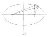
- An example of a doubly curved elementis given in FIGS. 3A & 3B.
- FIG. 3Ashows that the element can be elliptically curved in one-dimension
- FIG. 3Bshows that the element can be circularly curved in the other dimension. This provides point-to-point focusing.
- the ellipsoidal geometryprovides point to point focusing of monochromatic x-rays.
- Graded crystal elements with an ellipsoidal shapecan capture a large solid angle from a small x-ray source and form a micro monochromatic x-ray beam, useful for micro beam analysis, e.g., monochromatic micro XRF (X-ray Fluorescence), small spot XPS (X-ray Photoelectron Spectroscopy).
- the paraboloid geometryprovides a collimating x-ray beam from a point source.
- Crystal elements with graded d spacing planes curved to a paraboloid shapecan capture significant solid angle and produce a collimating beam from a pont-type laboratory source.
- the collimating beamcan be highly monochromatic with small divergence, which is required for high-resolution x-ray diffraction.
- graded crystal optics with a spherical geometrycan be applied to image hard x-rays.
- the combination of spherical optics, such as Schwarzschild optics,can provide strong demagnification and form a sub-micron x-ray beam based on a laboratory source.
- an x-ray reflective device shown in FIG. 1comprises a curved crystal 10 and support base 12.
- Crystal 10has a set of curved atomic reflection planes 14.
- atomic plane set 14is near parallel to the crystal surface 16 in the embodiment shown.
- the spacing between the atomic planes, dvaries continuously from d 1 at one end of the crystal to d 2 at the other end of the crystal.
- Values of d 1 and d 2are determined from the Bragg equation where the Bragg angles are the incident angles ⁇ 1 and ⁇ 2 , respectively.
- the Bragg angles of reflective planes 14 for x-ray photons of wavelength ⁇vary with the d spacing profiles.
- the configuration of the crystal surface 16can be spherical, ellipsoidal, paraboloidal, toroidal, or other type of doubly curved surface.
- the profile of the d spacing for the crystal planesis designed to allow the incident angles of monochromatic x-rays from a divergent laboratory source to match the Bragg angle on each point of the crystal surface.
- the optical device according to the present inventioncan be fabricated by bending a flat thin crystal slab 10 as shown in PIG. 2 with a desired d spacing profile to a preselected geometry.
- One bending methodis the fabrication process described in co-pending, commonly assigned United States Patent Application Serial No. 09/342,606 , entitled "Curved Optical Device and Method of Fabrication.”
- the variation of the d spacing of the crystal planescan be produced by growing a crystal made of two or more elements and changing the relative percentages of the two elements as the crystal is grown. For instance, the lattice parameter of a Si-Ge crystal Varies with a change in concentration of Ge.
- a crystal material with a graded lattice parametercan be obtained by growing a Si-Ge crystal and controlling the concentration of Ge during growth.
- Such crystal planesare commercial available and can be purchased, for example, from Virginia Semiconductor, Inc. of Fredericksburg, VA.
- FIG. 3AOne embodiment of the present invention providing point to point x-ray imaging is illustrated in FIG. 3A .
- Crystal planes 14are curved to an ellipsoidal shape and the d spacing of the planes varies along the direction parallel to the optical axis 2-2.
- the d spacing of reflection planeshas a maximum value do at the center point O and decreases as edge E is approached.
- the Bragg angle for x-rays of wavelength ⁇increases, which matches the increase of the incident angles from O to E for x-rays diverging from the left focus of the ellipse.
- a cross-section of the crystal taken along line 4-4is shown in FIG.
- FIG. 3Bshows an asymmetrical arrangement of a point to point focusing geometry, which provides demagnification of source S.
- the ellipsoidal crystal element in FIG. 3Acan be made by bending a flat crystal 10 (see FIG. 2 ) to an ellipsoid, where the d spacing of the flat crystal 10 varies along the X direction but is constant along the Y direction (see FIG. 2 ).
- the optical element shown in FIG. 3Amay be fabricated in two pieces such that two identical flat crystal slabs with graded d spacing from do to d E can be used as shown in the exploded view of FIG. 4 . In this embodiment, the two crystals are joined at O and the surface is ellipsoidal. This approach allows the grading to increase in one dimension. Conversely, the element in FIG. 3A requires a grading profile that increases and then decreases.
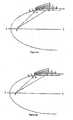
- FIG. 5AA curved crystal device with paraboloid geometry is shown in FIG. 5A .
- This deviceproduces a monochromatic collimating x-ray beam from a point source S.
- the d spacing of the reflection plane of the crystal 10is graded from a value of d 1 to d 2 .
- the d spacing profileis linear for the first order approximation and increases from point A to B.
- a collimated beamcan be directed to a focal spot as shown in FIG. 5B .
- the focusing and collimating of x-rayscan also be obtained with a spherical geometry at near normal incidence using crystalline planes with graded d spacing.
- Spherical mirrorsare well known as imaging devices for normal incident visible light optics.
- a conventional spherically bent crystalcan demagnify (or magnify) and collimate x-rays from a divergent x-ray source for some particular wavelength at near normal incidence.
- the numerical aperture of this type deviceis too small to be useful.
- the numerical aperturecan be improved substantially with the use of graded d spacing, doubly curved crystals in accordance with the present invention.
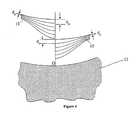
- FIG. 6Ashows a set of spherical curved crystal planes according to another embodiment of the present invention, which provides a demagnified image of the x-ray source.
- the d spacing of the crystal planeshas a symmetrical profile about the optical axis and varies along the transverse direction. It increases across the surface from points A to B.
- the normal projecting view along the optical axisis illustrated in FIG. 6B .
- the d spacing profile of this devicemay be difficult to obtain. In practice, it can be approximated by using multiple pieces of crystal slabs with a simple graded d profile as shown in FIG. 6C . Each piece of crystal is curved to a spherical shape with the reflection planes parallel to the surface.
- the d spacing profile of the reflection planesis one-dimensionally graded along the radial direction passing the center of each crystal. If an x-ray source is placed at the focus of the concave spherical device similar to the orientation shown in FIG. 6A , a collimating x-ray beam is obtained.
- the Schwarzschild configurationwhich is used to image soft x-rays in conjunction with a multilayer coating.
- Graded crystals with the Schwarzschild geometryprovide imaging for hard x-rays as shown in FIG. 7 .
- the reflection planes of primary crystal 18has a d spacing profile of d 1 (r) to reflect x-rays from a source emitting x-rays at a near normal incident angle.
- the reflection planes of the secondary crystal 20have the desired profile d 2 (r) to match the incident angles of the x-rays reflected off the primary crystal 18. This system produces a final image of the source at I.
Landscapes
- Engineering & Computer Science (AREA)
- Physics & Mathematics (AREA)
- Nanotechnology (AREA)
- General Engineering & Computer Science (AREA)
- High Energy & Nuclear Physics (AREA)
- Chemical & Material Sciences (AREA)
- Spectroscopy & Molecular Physics (AREA)
- Mathematical Physics (AREA)
- Theoretical Computer Science (AREA)
- Crystallography & Structural Chemistry (AREA)
- Analysing Materials By The Use Of Radiation (AREA)
- Lenses (AREA)
- Optical Filters (AREA)
- Optical Elements Other Than Lenses (AREA)
Description
- The present invention relates to doubly curved optical elements, and in particular, to a doubly curved optical device having multiple reflection planes separated by a spacing d which varies in at least one direction.
- Crystalline materials, which have periodic structure, can be used to reflect x-rays based on diffraction. The reflection of x-rays from crystal planes can only occur when the Bragg condition is met:

Whereλ is the x-ray wavelength,d is the spacing of reflection planes, θ is the incident angle with respect to the reflection planes, andn is the reflection order. Thed spacings for natural crystals and most synthetic crystals are constant. In order to reflect x-rays of the same wavelength efficiently, a crystal optical element must have a near constant incident angle with respect to the reflection planes of the crystal on every point of the surface. Crystal optics based on Bragg reflection have been widely used for x-ray monochromators and high-resolution spectroscopy. However, the applications of crystal optics for focusing and collimating x-rays from a laboratory source have been limited because of the strict requirement of the Bragg condition and the narrow rocking curve widths for most useful crystalline materials. - For many applications of microanalysis, an intense monochromatic x-ray beam based on a laboratory type source is needed. Three-dimensional focusing of x-rays from a laboratory source involves doubly bent crystal optics. The practical use of a toroidal crystal to focus 8 keV x-rays has been demonstrated recently with the use of a mica crystal based on the Johann type point to point focusing geometry. For example, reference an article byZ.W. Chen and D.B. Wittry entitled "Microanalysis by Monochromatic Microprobe X-ray Fluorescence-Physical Basis, Properties and Future Prospects", J. Appl. Phys., 84(2), page 1064 (1998). However, the Bragg condition cannot be satisfied on every point of the crystal using this approach due to the geometrical aberration of the Johann geometry in the Roland circle plane, which will limit the collection solid angle of the optic. The spot size of the focused beam is also limited by the geometrical aberration of the toroidal surface.
- On the other hand, a parallel monochromatic x-ray beam is useful for many x-ray diffraction applications. Conventional crystal optics with constant d spacing cannot provide efficient collimation of hard x-rays from a divergent source since the incident angle must vary from point to point for any type of collimating mirror. For high-resolution x-ray diffraction applications, the monochromaticity provided by conventional multilayer optics is relatively poor and the divergence is not small enough.
- Briefly summarized, the present invention comprises in one aspect an optically curved device which includes a plurality of curved atomic planes, at least some of which are separated by a spacingd which varies in at least one direction. The device further includes an optical surface which is doubly curved and disposed over the plurality of curved atomic planes. The spacingd varies in the at least one direction and is determined from a Bragg equation, where a Bragg angle is an incident angle of an x-ray from a source impinging on the optical surface on at least some points of the optical surface.
- To restate, it is an object of this invention to provide significantly improved curved crystal optical elements for focusing, collimating and imaging of x-rays. These curved crystal optics are characterized in that the lattice parameters change laterally in at least one direction. The variation of the crystal lattice parameter can be produced by growing a crystal made of two or more elements and changing the relative percentage of the two elements as the crystal is grown. By varying the d spacing laterally across the surface of a crystal optic, the Bragg angle θ on every point of the crystal can be matched to the incident angle exactly, which improves significantly the efficiency of curved crystal elements and eliminates any geometric aberration.
- The optical shapes of two-dimensionally curved graded crystal elements can be circular, ellipsoidal, parabolic, spherical, and other aspherical shapes. An example of a doubly curved element is given in
FIGS. 3A & 3B. FIG. 3A shows that the element can be elliptically curved in one-dimension, whileFIG. 3B shows that the element can be circularly curved in the other dimension. This provides point-to-point focusing. The ellipsoidal geometry provides point to point focusing of monochromatic x-rays. Graded crystal elements with an ellipsoidal shape can capture a large solid angle from a small x-ray source and form a micro monochromatic x-ray beam, useful for micro beam analysis, e.g., monochromatic micro XRF (X-ray Fluorescence), small spot XPS (X-ray Photoelectron Spectroscopy). The paraboloid geometry provides a collimating x-ray beam from a point source. Crystal elements with graded d spacing planes curved to a paraboloid shape can capture significant solid angle and produce a collimating beam from a pont-type laboratory source. Due to the narrow energy bandwidth of the crystal optic, the collimating beam can be highly monochromatic with small divergence, which is required for high-resolution x-ray diffraction. Finally, graded crystal optics with a spherical geometry can be applied to image hard x-rays. The combination of spherical optics, such as Schwarzschild optics, can provide strong demagnification and form a sub-micron x-ray beam based on a laboratory source. - The above-described objects, advantages and features of the present invention, as well as others, will be more readily understood from the following detailed description of certain preferred embodiments of the invention, when considered in conjunction with the accompanying drawings in which:
FIG. 1 is an exploded cross-sectional view of an x-ray optical element in accordance with the principles of the present invention;FIG. 2 is a flat crystal plate that has a set of atomic planes with gradedd spacing;FIG. 3A is a cross-sectional view of one embodiment of the present invention in which the graded crystal planes are curved to an ellipsoidal shape in one dimension, providing symmetrical point to point focusing of monochromatic x-rays;FIG. 3B is a cross-sectional view of the crystal ofFIG. 3A taken along line 4-4;FIG. 3C is an optical element similar to that inFIG. 3A , but with an asymmetrical configuration and providing demagnification of source S in accordance with an alternate embodiment of the present invention;FIG. 4 is an exploded view of an ellipsoidal crystal device that comprises two identical crystals with graded d spacings in accordance with the present invention;FIG. 5A is a cross-sectional view of another embodiment of an optical element in accordance with the present invention showing graded crystal planes curved to paraboloid shape and providing a collimating beam from a point x-ray source;FIG. 5B is a cross-sectional view of another embodiment of an optical element in accordance with the present invention showing graded crystal planes curved to paraboloid shape, and accepting a collimating beam and directing it to a focal spot;FIG. 6A depicts a spherical optical element in accordance with the present invention for imaging a source with close to normal angle incident;FIG. 6B is a cross-sectional view of the spherical device ofFIG. 6A taken line c-c;FIG. 6C is a cross-sectional view of a spherical device comprising multiple pieces of crystal slabs with simple graded d profile in accordance with another embodiment of the present invention; andFIG. 7 shows a configuration of two graded concave crystals in accordance with the present invention for strong demagnification imaging.- In accordance with this invention, an x-ray reflective device shown in
FIG. 1 comprises acurved crystal 10 andsupport base 12.Crystal 10 has a set of curved atomic reflection planes 14. On every point of the crystal surface, atomic plane set 14 is near parallel to thecrystal surface 16 in the embodiment shown. The spacing between the atomic planes,d, varies continuously fromd1 at one end of the crystal tod2 at the other end of the crystal. Values ofd1 and d2 are determined from the Bragg equation where the Bragg angles are the incident angles θ1 and θ2, respectively. Accordi.ng to the Bragg equation, the Bragg angles ofreflective planes 14 for x-ray photons of wavelength λ vary with the d spacing profiles. The configuration of thecrystal surface 16 can be spherical, ellipsoidal, paraboloidal, toroidal, or other type of doubly curved surface. The profile of the d spacing for the crystal planes is designed to allow the incident angles of monochromatic x-rays from a divergent laboratory source to match the Bragg angle on each point of the crystal surface. - The optical device according to the present invention can be fabricated by bending a flat
thin crystal slab 10 as shown in PIG. 2 with a desired d spacing profile to a preselected geometry. One bending method is the fabrication process described in co-pending, commonly assigned United States Patent Application Serial No.09/342,606 - One embodiment of the present invention providing point to point x-ray imaging is illustrated in
FIG. 3A . Crystal planes 14 are curved to an ellipsoidal shape and the d spacing of the planes varies along the direction parallel to the optical axis 2-2. For the symmetrical configuration shown inFIG. 3A , thed spacing of reflection planes has a maximum valuedo at the center point O and decreases as edge E is approached. With the decrease of thed value from the center O of the crystal to the edge E, the Bragg angle for x-rays of wavelength λ increases, which matches the increase of the incident angles from O to E for x-rays diverging from the left focus of the ellipse. A cross-section of the crystal taken along line 4-4 is shown inFIG. 3B . In this plane, the crystal planes are circular and the d spacing does not vary.FIG. 3C shows an asymmetrical arrangement of a point to point focusing geometry, which provides demagnification of source S. The ellipsoidal crystal element inFIG. 3A can be made by bending a flat crystal 10 (seeFIG. 2 ) to an ellipsoid, where the d spacing of theflat crystal 10 varies along the X direction but is constant along the Y direction (seeFIG. 2 ). The optical element shown inFIG. 3A may be fabricated in two pieces such that two identical flat crystal slabs with graded d spacing from do todE can be used as shown in the exploded view ofFIG. 4 . In this embodiment, the two crystals are joined at O and the surface is ellipsoidal. This approach allows the grading to increase in one dimension. Conversely, the element inFIG. 3A requires a grading profile that increases and then decreases. - A curved crystal device with paraboloid geometry is shown in
FIG. 5A . This device produces a monochromatic collimating x-ray beam from a point source S. Thed spacing of the reflection plane of thecrystal 10 is graded from a value ofd1 tod2. To satisfy the Bragg condition, the d spacing profile is linear for the first order approximation and increases from point A to B. Alternatively, a collimated beam can be directed to a focal spot as shown inFIG. 5B . - The focusing and collimating of x-rays can also be obtained with a spherical geometry at near normal incidence using crystalline planes with graded d spacing. Spherical mirrors are well known as imaging devices for normal incident visible light optics. A conventional spherically bent crystal can demagnify (or magnify) and collimate x-rays from a divergent x-ray source for some particular wavelength at near normal incidence. However, the numerical aperture of this type device is too small to be useful. The numerical aperture can be improved substantially with the use of graded d spacing, doubly curved crystals in accordance with the present invention.
FIG. 6A shows a set of spherical curved crystal planes according to another embodiment of the present invention, which provides a demagnified image of the x-ray source. The d spacing of the crystal planes has a symmetrical profile about the optical axis and varies along the transverse direction. It increases across the surface from points A to B. The normal projecting view along the optical axis is illustrated inFIG. 6B . Thed spacing profile of this device may be difficult to obtain. In practice, it can be approximated by using multiple pieces of crystal slabs with a simple graded d profile as shown inFIG. 6C . Each piece of crystal is curved to a spherical shape with the reflection planes parallel to the surface. The d spacing profile of the reflection planes is one-dimensionally graded along the radial direction passing the center of each crystal. If an x-ray source is placed at the focus of the concave spherical device similar to the orientation shown inFIG. 6A , a collimating x-ray beam is obtained.- Strong demagnification can be obtained if two spherical crystal devices are combined. One preferred geometry is the Schwarzschild configuration which is used to image soft x-rays in conjunction with a multilayer coating. Graded crystals with the Schwarzschild geometry provide imaging for hard x-rays as shown in
FIG. 7 . The reflection planes ofprimary crystal 18 has a d spacing profile ofd1(r) to reflect x-rays from a source emitting x-rays at a near normal incident angle. The reflection planes of thesecondary crystal 20 have the desired profiled2(r) to match the incident angles of the x-rays reflected off theprimary crystal 18. This system produces a final image of the source at I. - While the invention has been described in detail herein in accordance with certain preferred embodiments thereof, many modifications and changes therein may be effected by those skilled in the art. Accordingly, it is intended by the appended claims to cover all such modifications and changes as fall within the scope of the invention as claimed.

Claims (13)
- Doubly curved optical device (10) comprising:a plurality of curved atomic planes (14), at least some curved atomic planes (14) being separated by a spacing d;andan optical surface (16) disposed over said plurality of curved atomic planes (14), said optical surface (16) being doubly curved;characterised in that said spacing d varies in at least one lateral direction across the optical surface and is determined from a Bragg equation, where a Bragg angle is an incident angle of an x-ray from a source impinging on said optical surface (16) on each of at least some points of said optical surface (16).
- Doubly curved optical device (10) in accordance with claim 1, wherein said spacing d varies in said at least one direction to achieve maximum reflectivity of x-rays from a divergent source.
- Doubly curved optical device (10) in accordance with any of the preceding claims, wherein said doubly curved optical surface (16) comprises one of an elliptic, parabolic, spheric or aspheric profile.
- Doubly curved optical device (10) in accordance with claim 3, wherein said doubly curved optical surface (16) comprises an elliptical profile and said doubly curved optical device (10) provides point to point focusing of x-rays.
- Doubly curved optical device (10) in accordance with claim 3, wherein said doubly curved optical surface (16) comprises a parabolic profile and said doubly curved optical device (10) provides collimation of x-rays from a point source.
- Doubly curved optical device (10) in accordance with claim 3, wherein said doubly curved optical surface (16) comprises a spherical profile and said doubly curved optical device (10) provides imaging of x-rays.
- Doubly curved optical device (10) in accordance with claim 3, wherein said doubly curved optical surface has a profile adapted for at least one of point to point focusing, directing a divergent x-ray beam from a point source to a collimated beam, directing an x-ray beam from a point source to an x-ray beam with a different divergence angle, or imaging of x-rays.
- Doubly curved optical device (10) in accordance with any of the preceding claims, wherein said doubly curved optical device (10) comprises an SiGe crystal, and wherein a ratio of silicon to germanium in said at least some curved atomic planes (14) separated by said varying spacing d varies across said doubly curved optical device (10).
- Doubly curved optical device (10) in accordance with any of the preceding claims, wherein said doubly curved optical device (10) comprises at least a first crystal piece (18) and a second crystal piece (20), wherein each crystal piece includes said plurality of curved atomic planes (14) and said optical surface (16) disposed thereover.
- Doubly curved optical device (10) in accordance with claim 9, wherein said first crystal piece (18) and said second crystal piece (20) are disposed symmetrical about a center axis of said doubly curved optical device (10).
- Doubly curved optical device (10) in accordance with claim 9, wherein said first crystal piece (18) comprises a first spherical optic and said second crystal piece (20) comprises a second spherical optic, wherein said first spherical optic and said second spherical optic are configured as Schwarzschild optics, and wherein said doubly curved optical device (10) provides demagnification of x-rays from said divergent source.
- Doubly curved optical device (10) in accordance with any of the preceding claims, wherein said spacing d varies in two dimensions for matching of incident angles of x-rays from said divergent source impinging on said optical surface (16) with a Bragg angle on each of a plurality of points disposed across said optical surface (16).
- Doubly curved optical device (10) in accordance with claim 12, wherein said plurality of points are disposed in a radial distribution across said optical surface (16).
Applications Claiming Priority (3)
| Application Number | Priority Date | Filing Date | Title |
|---|---|---|---|
| US450323 | 1995-05-25 | ||
| US09/450,323US6317483B1 (en) | 1999-11-29 | 1999-11-29 | Doubly curved optical device with graded atomic planes |
| PCT/US2000/032336WO2001039211A1 (en) | 1999-11-29 | 2000-11-27 | Doubly curved optical device with graded atomic planes |
Publications (2)
| Publication Number | Publication Date |
|---|---|
| EP1234310A1 EP1234310A1 (en) | 2002-08-28 |
| EP1234310B1true EP1234310B1 (en) | 2012-11-14 |
Family
ID=23787638
Family Applications (1)
| Application Number | Title | Priority Date | Filing Date |
|---|---|---|---|
| EP00980804AExpired - LifetimeEP1234310B1 (en) | 1999-11-29 | 2000-11-27 | Doubly curved optical device with graded atomic planes |
Country Status (5)
| Country | Link |
|---|---|
| US (1) | US6317483B1 (en) |
| EP (1) | EP1234310B1 (en) |
| JP (2) | JP2003515729A (en) |
| AU (1) | AU1802101A (en) |
| WO (1) | WO2001039211A1 (en) |
Families Citing this family (42)
| Publication number | Priority date | Publication date | Assignee | Title |
|---|---|---|---|---|
| US6829327B1 (en)* | 2000-09-22 | 2004-12-07 | X-Ray Optical Systems, Inc. | Total-reflection x-ray fluorescence apparatus and method using a doubly-curved optic |
| AU2002314278A1 (en)* | 2001-06-01 | 2002-12-09 | Xenocs | Hybrid optical component for x ray applications and method associated therewith |
| CA2489646C (en)* | 2001-06-19 | 2010-02-09 | X-Ray Optical Systems, Inc. | Wavelength dispersive xrf system using focusing optic for excitation and a focusing monochromator for collection |
| US20030012336A1 (en)* | 2001-06-20 | 2003-01-16 | Cash Webster C. | X-ray concentrator for therapy |
| JP4657506B2 (en)* | 2001-06-27 | 2011-03-23 | 株式会社リガク | X-ray spectroscopy method and X-ray spectrometer |
| US6781060B2 (en) | 2002-07-26 | 2004-08-24 | X-Ray Optical Systems Incorporated | Electrical connector, a cable sleeve, and a method for fabricating an electrical connection |
| FR2841371B1 (en)* | 2002-06-19 | 2004-10-22 | Xenocs | OPTICAL ASSEMBLY AND ASSOCIATED METHOD |
| FR2850171B1 (en)* | 2003-01-21 | 2005-04-08 | Xenocs | OPTICAL DEVICE FOR X-RAY APPLICATIONS |
| JP2005530170A (en)* | 2002-06-19 | 2005-10-06 | グズノク | Optical assembly and manufacturing method thereof |
| AU2003256831A1 (en)* | 2002-08-02 | 2004-02-23 | X-Ray Optical Systems, Inc. | An optical device for directing x-rays having a plurality of optical crystals |
| DE10254026C5 (en)* | 2002-11-20 | 2009-01-29 | Incoatec Gmbh | Reflector for X-radiation |
| EP1732086A4 (en)* | 2004-02-12 | 2008-04-16 | Japan Science & Tech Agency | X-RAY MOUSE PROCESSING DEVICE AND X-RAY MOUSE PROCESSING METHOD |
| KR101231731B1 (en)* | 2004-09-21 | 2013-02-08 | 조르단 밸리 세미컨덕터즈 리미티드 | Multifunction x-ray analysis system |
| WO2007016484A2 (en) | 2005-08-01 | 2007-02-08 | The Research Foundation Of State University Of New York | X-ray imaging systems employing point-focusing, curved monochromating optics |
| CN101278360B (en)* | 2005-08-04 | 2011-07-27 | X射线光学系统公司 | Monochromatic x-ray micro beam for trace element mapping |
| US7555098B2 (en)* | 2007-05-02 | 2009-06-30 | HD Technologies Inc. | Method and apparatus for X-ray fluorescence analysis and detection |
| US7742566B2 (en)* | 2007-12-07 | 2010-06-22 | General Electric Company | Multi-energy imaging system and method using optic devices |
| WO2009126868A1 (en)* | 2008-04-11 | 2009-10-15 | Rigaku Innovative Technologies, Inc. | X-ray generator with polycapillary optic |
| JP5344123B2 (en)* | 2008-07-18 | 2013-11-20 | 独立行政法人 宇宙航空研究開発機構 | X-ray reflector, X-ray reflector, and method for producing X-ray reflector |
| US8050380B2 (en)* | 2009-05-05 | 2011-11-01 | Media Lario, S.R.L. | Zone-optimized mirrors and optical systems using same |
| CN102460135A (en)* | 2009-06-03 | 2012-05-16 | 特莫尼托恩分析仪器股份有限公司 | X-ray system and method with detector inside focusing element |
| US8243878B2 (en)* | 2010-01-07 | 2012-08-14 | Jordan Valley Semiconductors Ltd. | High-resolution X-ray diffraction measurement with enhanced sensitivity |
| US8687766B2 (en) | 2010-07-13 | 2014-04-01 | Jordan Valley Semiconductors Ltd. | Enhancing accuracy of fast high-resolution X-ray diffractometry |
| US8437450B2 (en) | 2010-12-02 | 2013-05-07 | Jordan Valley Semiconductors Ltd. | Fast measurement of X-ray diffraction from tilted layers |
| US8781070B2 (en) | 2011-08-11 | 2014-07-15 | Jordan Valley Semiconductors Ltd. | Detection of wafer-edge defects |
| JP6084222B2 (en) | 2011-08-15 | 2017-02-22 | エックス−レイ オプティカル システムズ インコーポレーテッド | Sample viscosity / flow rate control for heavy samples and its X-ray analysis application |
| CN103946693B (en) | 2011-10-06 | 2017-05-03 | X射线光学系统公司 | Mobile transport and shielding apparatus for removable x-ray analyzer |
| CN103765201B (en) | 2011-10-26 | 2017-11-07 | X射线光学系统公司 | Support structure for the X-ray analysis engine and analyzer and highly aligned monochromatic X-ray optics |
| CN104272424A (en)* | 2012-02-28 | 2015-01-07 | X射线光学系统公司 | X-ray analyzer with multiple excitation bands generated using multi-material x-ray tube anode and monochromator optics |
| CZ2012265A3 (en)* | 2012-04-17 | 2013-07-03 | Ceské vysoké ucení technické v Praze, Fakulta jaderná a fyzikálne inzenýrská | X-ray telescope |
| WO2015027225A1 (en) | 2013-08-23 | 2015-02-26 | The Schepens Eye Research Institute, Inc. | Spatial modeling of visual fields |
| US9726624B2 (en) | 2014-06-18 | 2017-08-08 | Bruker Jv Israel Ltd. | Using multiple sources/detectors for high-throughput X-ray topography measurement |
| WO2016103834A1 (en)* | 2014-12-25 | 2016-06-30 | 株式会社リガク | Oblique-incidence x-ray fluorescence analysis device and method |
| JP6069609B2 (en)* | 2015-03-26 | 2017-02-01 | 株式会社リガク | Double-curved X-ray condensing element and its constituent, double-curved X-ray spectroscopic element and method for producing the constituent |
| US10018577B2 (en) | 2015-04-03 | 2018-07-10 | Mission Support and Tests Services, LLC | Methods and systems for imaging bulk motional velocities in plasmas |
| US9945795B2 (en) | 2016-03-18 | 2018-04-17 | National Security Technologies, Inc. | Crystals for krypton helium-alpha line emission microscopy |
| US10677744B1 (en)* | 2016-06-03 | 2020-06-09 | U.S. Department Of Energy | Multi-cone x-ray imaging Bragg crystal spectrometer |
| DE102017202802A1 (en)* | 2017-02-21 | 2018-08-23 | Carl Zeiss Smt Gmbh | Lens and optical system with such a lens |
| JP7394464B2 (en)* | 2018-07-04 | 2023-12-08 | 株式会社リガク | Fluorescent X-ray analyzer |
| EP3603516A1 (en)* | 2018-08-02 | 2020-02-05 | Siemens Healthcare GmbH | X-ray equipment and method for operating same |
| US20220201830A1 (en) | 2020-12-23 | 2022-06-23 | X-Ray Optical Systems, Inc. | X-ray source assembly with enhanced temperature control for output stability |
| US12247934B2 (en) | 2022-07-29 | 2025-03-11 | X-Ray Optical Systems, Inc. | Polarized, energy dispersive x-ray fluorescence system and method |
Family Cites Families (17)
| Publication number | Priority date | Publication date | Assignee | Title |
|---|---|---|---|---|
| US4599741A (en) | 1983-11-04 | 1986-07-08 | USC--Dept. of Materials Science | System for local X-ray excitation by monochromatic X-rays |
| NL8501181A (en) | 1985-04-24 | 1986-11-17 | Philips Nv | CRYSTAL FOR A ROENT GENAL ANALYSIS DEVICE. |
| JPS6361200A (en)* | 1986-09-01 | 1988-03-17 | 日本電信電話株式会社 | X-ray condensing multilayer film spectroscopic element |
| JPH0833497B2 (en)* | 1987-03-25 | 1996-03-29 | 株式会社島津製作所 | X-ray curved crystal |
| NL8801019A (en) | 1988-04-20 | 1989-11-16 | Philips Nv | ROENTGEN SPECTROMETER WITH DOUBLE-CURVED CRYSTAL. |
| JP2569447B2 (en)* | 1988-11-28 | 1997-01-08 | 株式会社ニコン | Manufacturing method of multilayer mirror |
| JPH02160517A (en) | 1988-12-14 | 1990-06-20 | Sumitomo Bakelite Co Ltd | Manufacture of grooved substrate for optical disk |
| JPH02217801A (en)* | 1989-02-17 | 1990-08-30 | Mitsubishi Electric Corp | Optical element consisting of multilayered films of curved type |
| JPH0372298A (en)* | 1989-08-14 | 1991-03-27 | Nikon Corp | Manufacturing method of multilayer reflective mirror |
| JP2530029B2 (en)* | 1989-09-26 | 1996-09-04 | オリンパス光学工業株式会社 | Multilayer spectrometer |
| US5027377A (en)* | 1990-01-09 | 1991-06-25 | The United States Of America As Represented By The United States Department Of Energy | Chromatic X-ray magnifying method and apparatus by Bragg reflective planes on the surface of Abbe sphere |
| JP2968995B2 (en)* | 1990-11-30 | 1999-11-02 | 株式会社リコー | Multi-wavelength spectroscopy element |
| US5646976A (en) | 1994-08-01 | 1997-07-08 | Osmic, Inc. | Optical element of multilayered thin film for X-rays and neutrons |
| US5757882A (en)* | 1995-12-18 | 1998-05-26 | Osmic, Inc. | Steerable x-ray optical system |
| US5737137A (en) | 1996-04-01 | 1998-04-07 | The Regents Of The University Of California | Critical illumination condenser for x-ray lithography |
| US5843235A (en) | 1996-09-11 | 1998-12-01 | Honeywell Inc. | Apparatus for forming a deposited curver coating on a substrate and mirror |
| DE19833524B4 (en)* | 1998-07-25 | 2004-09-23 | Bruker Axs Gmbh | X-ray analyzer with gradient multilayer mirror |
- 1999
- 1999-11-29USUS09/450,323patent/US6317483B1/ennot_activeExpired - Lifetime
- 2000
- 2000-11-27AUAU18021/01Apatent/AU1802101A/ennot_activeAbandoned
- 2000-11-27EPEP00980804Apatent/EP1234310B1/ennot_activeExpired - Lifetime
- 2000-11-27JPJP2001540791Apatent/JP2003515729A/enactivePending
- 2000-11-27WOPCT/US2000/032336patent/WO2001039211A1/enactiveApplication Filing
- 2006
- 2006-09-20JPJP2006254908Apatent/JP2007011403A/enactivePending
Also Published As
| Publication number | Publication date |
|---|---|
| JP2007011403A (en) | 2007-01-18 |
| JP2003515729A (en) | 2003-05-07 |
| AU1802101A (en) | 2001-06-04 |
| WO2001039211A1 (en) | 2001-05-31 |
| US6317483B1 (en) | 2001-11-13 |
| EP1234310A1 (en) | 2002-08-28 |
Similar Documents
| Publication | Publication Date | Title |
|---|---|---|
| EP1234310B1 (en) | Doubly curved optical device with graded atomic planes | |
| EP0322408B1 (en) | Instrumentation for conditioning x-ray or neutron beams | |
| Schroer et al. | Focusing hard x rays to nanometer dimensions by adiabatically focusing lenses | |
| Sparks Jr et al. | X-ray monochromator geometry for focusing synchrotron radiation above 10 keV | |
| US7430277B2 (en) | Optical device for X-ray applications | |
| JP2013210377A (en) | Beam adjustment system | |
| EP0138440A2 (en) | Point source X-ray focusing device | |
| US20110280530A1 (en) | X-ray generator with polycapillary optic | |
| KR102133912B1 (en) | Optical design method for x-ray focusing system using rotating mirror, and x-ray focusing system | |
| WO2001046961A1 (en) | X-ray system and method | |
| JP2013531242A (en) | X-ray optical system with adjustable convergence and focal spot size | |
| Suzuki et al. | High-energy x-ray microbeam with total-reflection mirror optics | |
| US7242746B2 (en) | Method for manufacturing a reflector for X-ray radiation | |
| Podorov et al. | Optimized polychromatic x-ray imaging with asymmetrically cutbent crystals | |
| Høghøj et al. | Focusing of hard X-rays with a WSi supermirror | |
| Alianelli et al. | Development of Hard X-ray Focusing Optics at Diamond Light Source | |
| CN103559926B (en) | A kind of phase place flap-type nano-focusing unit and method for designing thereof | |
| EP1614121B1 (en) | A refractive x-ray element | |
| JP2003262832A (en) | Diffraction compensation using reflector with pattern | |
| AU612985B2 (en) | Instrumentation for conditioning x-ray or neutron beams | |
| US11789187B2 (en) | Method for producing a multilayer Laue lens | |
| US5914998A (en) | X-ray microbeam generating method and device for the same | |
| JP6116407B2 (en) | X-ray focusing apparatus and X-ray apparatus | |
| JPH02146000A (en) | Manufacture of reflecting mirror with mutilayered membrane | |
| JPH06300897A (en) | X-ray optical device |
Legal Events
| Date | Code | Title | Description |
|---|---|---|---|
| PUAI | Public reference made under article 153(3) epc to a published international application that has entered the european phase | Free format text:ORIGINAL CODE: 0009012 | |
| 17P | Request for examination filed | Effective date:20020517 | |
| AK | Designated contracting states | Kind code of ref document:A1 Designated state(s):AT BE CH CY DE DK ES FI FR GB GR IE IT LI LU MC NL PT | |
| AX | Request for extension of the european patent | Free format text:AL PAYMENT 20020517;LT PAYMENT 20020517;LV PAYMENT 20020517;MK PAYMENT 20020517;RO PAYMENT 20020517;SI PAYMENT 20020517 | |
| RIN1 | Information on inventor provided before grant (corrected) | Inventor name:CHEN, ZEWU | |
| 17Q | First examination report despatched | Effective date:20090428 | |
| GRAP | Despatch of communication of intention to grant a patent | Free format text:ORIGINAL CODE: EPIDOSNIGR1 | |
| GRAS | Grant fee paid | Free format text:ORIGINAL CODE: EPIDOSNIGR3 | |
| GRAA | (expected) grant | Free format text:ORIGINAL CODE: 0009210 | |
| AK | Designated contracting states | Kind code of ref document:B1 Designated state(s):AT BE CH CY DE DK ES FI FR GB GR IE IT LI LU MC NL PT | |
| AX | Request for extension of the european patent | Extension state:AL LT LV MK RO SI | |
| REG | Reference to a national code | Ref country code:GB Ref legal event code:FG4D | |
| REG | Reference to a national code | Ref country code:CH Ref legal event code:EP Ref country code:AT Ref legal event code:REF Ref document number:584355 Country of ref document:AT Kind code of ref document:T Effective date:20121115 | |
| REG | Reference to a national code | Ref country code:IE Ref legal event code:FG4D | |
| REG | Reference to a national code | Ref country code:DE Ref legal event code:R096 Ref document number:60047640 Country of ref document:DE Effective date:20130110 | |
| REG | Reference to a national code | Ref country code:NL Ref legal event code:T3 | |
| REG | Reference to a national code | Ref country code:AT Ref legal event code:MK05 Ref document number:584355 Country of ref document:AT Kind code of ref document:T Effective date:20121114 | |
| REG | Reference to a national code | Ref country code:LT Ref legal event code:MG9D | |
| PG25 | Lapsed in a contracting state [announced via postgrant information from national office to epo] | Ref country code:ES Free format text:LAPSE BECAUSE OF FAILURE TO SUBMIT A TRANSLATION OF THE DESCRIPTION OR TO PAY THE FEE WITHIN THE PRESCRIBED TIME-LIMIT Effective date:20130225 Ref country code:FI Free format text:LAPSE BECAUSE OF FAILURE TO SUBMIT A TRANSLATION OF THE DESCRIPTION OR TO PAY THE FEE WITHIN THE PRESCRIBED TIME-LIMIT Effective date:20121114 | |
| PG25 | Lapsed in a contracting state [announced via postgrant information from national office to epo] | Ref country code:BE Free format text:LAPSE BECAUSE OF FAILURE TO SUBMIT A TRANSLATION OF THE DESCRIPTION OR TO PAY THE FEE WITHIN THE PRESCRIBED TIME-LIMIT Effective date:20121114 Ref country code:PT Free format text:LAPSE BECAUSE OF FAILURE TO SUBMIT A TRANSLATION OF THE DESCRIPTION OR TO PAY THE FEE WITHIN THE PRESCRIBED TIME-LIMIT Effective date:20130314 Ref country code:CY Free format text:LAPSE BECAUSE OF FAILURE TO SUBMIT A TRANSLATION OF THE DESCRIPTION OR TO PAY THE FEE WITHIN THE PRESCRIBED TIME-LIMIT Effective date:20121114 Ref country code:GR Free format text:LAPSE BECAUSE OF FAILURE TO SUBMIT A TRANSLATION OF THE DESCRIPTION OR TO PAY THE FEE WITHIN THE PRESCRIBED TIME-LIMIT Effective date:20130215 | |
| PG25 | Lapsed in a contracting state [announced via postgrant information from national office to epo] | Ref country code:AT Free format text:LAPSE BECAUSE OF FAILURE TO SUBMIT A TRANSLATION OF THE DESCRIPTION OR TO PAY THE FEE WITHIN THE PRESCRIBED TIME-LIMIT Effective date:20121114 | |
| REG | Reference to a national code | Ref country code:CH Ref legal event code:PL | |
| PG25 | Lapsed in a contracting state [announced via postgrant information from national office to epo] | Ref country code:DK Free format text:LAPSE BECAUSE OF FAILURE TO SUBMIT A TRANSLATION OF THE DESCRIPTION OR TO PAY THE FEE WITHIN THE PRESCRIBED TIME-LIMIT Effective date:20121114 Ref country code:CH Free format text:LAPSE BECAUSE OF NON-PAYMENT OF DUE FEES Effective date:20121130 Ref country code:LI Free format text:LAPSE BECAUSE OF NON-PAYMENT OF DUE FEES Effective date:20121130 | |
| REG | Reference to a national code | Ref country code:IE Ref legal event code:MM4A | |
| PG25 | Lapsed in a contracting state [announced via postgrant information from national office to epo] | Ref country code:IT Free format text:LAPSE BECAUSE OF FAILURE TO SUBMIT A TRANSLATION OF THE DESCRIPTION OR TO PAY THE FEE WITHIN THE PRESCRIBED TIME-LIMIT Effective date:20121114 | |
| PLBE | No opposition filed within time limit | Free format text:ORIGINAL CODE: 0009261 | |
| STAA | Information on the status of an ep patent application or granted ep patent | Free format text:STATUS: NO OPPOSITION FILED WITHIN TIME LIMIT | |
| 26N | No opposition filed | Effective date:20130815 | |
| PG25 | Lapsed in a contracting state [announced via postgrant information from national office to epo] | Ref country code:IE Free format text:LAPSE BECAUSE OF NON-PAYMENT OF DUE FEES Effective date:20121127 | |
| REG | Reference to a national code | Ref country code:DE Ref legal event code:R097 Ref document number:60047640 Country of ref document:DE Effective date:20130815 | |
| PG25 | Lapsed in a contracting state [announced via postgrant information from national office to epo] | Ref country code:MC Free format text:LAPSE BECAUSE OF NON-PAYMENT OF DUE FEES Effective date:20121130 | |
| PG25 | Lapsed in a contracting state [announced via postgrant information from national office to epo] | Ref country code:LU Free format text:LAPSE BECAUSE OF NON-PAYMENT OF DUE FEES Effective date:20121127 | |
| REG | Reference to a national code | Ref country code:DE Ref legal event code:R082 Ref document number:60047640 Country of ref document:DE Representative=s name:ANDRAE WESTENDORP PATENTANWAELTE PARTNERSCHAFT, DE Ref country code:DE Ref legal event code:R082 Ref document number:60047640 Country of ref document:DE Representative=s name:FRIESE GOEDEN, DE Ref country code:DE Ref legal event code:R082 Ref document number:60047640 Country of ref document:DE Representative=s name:FRIESE GOEDEN PATENTANWAELTE PARTGMBB, DE | |
| REG | Reference to a national code | Ref country code:FR Ref legal event code:PLFP Year of fee payment:16 | |
| REG | Reference to a national code | Ref country code:DE Ref legal event code:R082 Ref document number:60047640 Country of ref document:DE Representative=s name:FRIESE GOEDEN, DE Ref country code:DE Ref legal event code:R082 Ref document number:60047640 Country of ref document:DE Representative=s name:FRIESE GOEDEN PATENTANWAELTE PARTGMBB, DE | |
| REG | Reference to a national code | Ref country code:FR Ref legal event code:PLFP Year of fee payment:17 | |
| PGFP | Annual fee paid to national office [announced via postgrant information from national office to epo] | Ref country code:NL Payment date:20161126 Year of fee payment:17 Ref country code:FR Payment date:20161123 Year of fee payment:17 Ref country code:GB Payment date:20161128 Year of fee payment:17 Ref country code:DE Payment date:20161123 Year of fee payment:17 | |
| REG | Reference to a national code | Ref country code:DE Ref legal event code:R119 Ref document number:60047640 Country of ref document:DE | |
| REG | Reference to a national code | Ref country code:NL Ref legal event code:MM Effective date:20171201 | |
| GBPC | Gb: european patent ceased through non-payment of renewal fee | Effective date:20171127 | |
| REG | Reference to a national code | Ref country code:FR Ref legal event code:ST Effective date:20180731 | |
| PG25 | Lapsed in a contracting state [announced via postgrant information from national office to epo] | Ref country code:DE Free format text:LAPSE BECAUSE OF NON-PAYMENT OF DUE FEES Effective date:20180602 Ref country code:NL Free format text:LAPSE BECAUSE OF NON-PAYMENT OF DUE FEES Effective date:20171201 Ref country code:FR Free format text:LAPSE BECAUSE OF NON-PAYMENT OF DUE FEES Effective date:20171130 | |
| PG25 | Lapsed in a contracting state [announced via postgrant information from national office to epo] | Ref country code:GB Free format text:LAPSE BECAUSE OF NON-PAYMENT OF DUE FEES Effective date:20171127 |