EP1207378B1 - Semiconductor pressure sensor and pressure sensing device - Google Patents
Semiconductor pressure sensor and pressure sensing deviceDownload PDFInfo
- Publication number
- EP1207378B1 EP1207378B1EP99938551AEP99938551AEP1207378B1EP 1207378 B1EP1207378 B1EP 1207378B1EP 99938551 AEP99938551 AEP 99938551AEP 99938551 AEP99938551 AEP 99938551AEP 1207378 B1EP1207378 B1EP 1207378B1
- Authority
- EP
- European Patent Office
- Prior art keywords
- pressure
- film
- oxide film
- detector
- diaphragm
- Prior art date
- Legal status (The legal status is an assumption and is not a legal conclusion. Google has not performed a legal analysis and makes no representation as to the accuracy of the status listed.)
- Expired - Lifetime
Links
- 239000004065semiconductorSubstances0.000titledescription8
- 229910021420polycrystalline siliconInorganic materials0.000claimsdescription36
- 229920005591polysiliconPolymers0.000claimsdescription36
- VYPSYNLAJGMNEJ-UHFFFAOYSA-NSilicium dioxideChemical compoundO=[Si]=OVYPSYNLAJGMNEJ-UHFFFAOYSA-N0.000claimsdescription26
- 229910052814silicon oxideInorganic materials0.000claimsdescription26
- 239000000758substrateSubstances0.000claimsdescription25
- 238000000034methodMethods0.000claimsdescription19
- 238000005530etchingMethods0.000claimsdescription15
- 238000007789sealingMethods0.000claimsdescription12
- 238000012937correctionMethods0.000claimsdescription9
- 229910052751metalInorganic materials0.000claimsdescription2
- 239000002184metalSubstances0.000claimsdescription2
- 239000003990capacitorSubstances0.000description27
- 238000004519manufacturing processMethods0.000description15
- 238000005229chemical vapour depositionMethods0.000description13
- 230000008859changeEffects0.000description12
- 238000001514detection methodMethods0.000description11
- 229910052581Si3N4Inorganic materials0.000description10
- HQVNEWCFYHHQES-UHFFFAOYSA-Nsilicon nitrideChemical compoundN12[Si]34N5[Si]62N3[Si]51N64HQVNEWCFYHHQES-UHFFFAOYSA-N0.000description10
- 239000003566sealing materialSubstances0.000description9
- XUIMIQQOPSSXEZ-UHFFFAOYSA-NSiliconChemical compound[Si]XUIMIQQOPSSXEZ-UHFFFAOYSA-N0.000description8
- 229910052710siliconInorganic materials0.000description8
- 239000010703siliconSubstances0.000description8
- 238000001259photo etchingMethods0.000description6
- 230000008569processEffects0.000description6
- OAICVXFJPJFONN-UHFFFAOYSA-NPhosphorusChemical compound[P]OAICVXFJPJFONN-UHFFFAOYSA-N0.000description5
- 230000001133accelerationEffects0.000description5
- 239000012535impuritySubstances0.000description5
- 229910052698phosphorusInorganic materials0.000description5
- 239000011574phosphorusSubstances0.000description5
- 230000002123temporal effectEffects0.000description5
- 238000005259measurementMethods0.000description3
- 239000000853adhesiveSubstances0.000description2
- 230000001070adhesive effectEffects0.000description2
- 229910052782aluminiumInorganic materials0.000description2
- XAGFODPZIPBFFR-UHFFFAOYSA-NaluminiumChemical compound[Al]XAGFODPZIPBFFR-UHFFFAOYSA-N0.000description2
- 230000015572biosynthetic processEffects0.000description2
- 238000009792diffusion processMethods0.000description2
- 239000000446fuelSubstances0.000description2
- 239000003502gasolineSubstances0.000description2
- 238000009413insulationMethods0.000description2
- 238000004806packaging method and processMethods0.000description2
- 239000002245particleSubstances0.000description2
- 239000005365phosphate glassSubstances0.000description2
- 230000002265preventionEffects0.000description2
- 230000004044responseEffects0.000description2
- XLYOFNOQVPJJNP-UHFFFAOYSA-NwaterSubstancesOXLYOFNOQVPJJNP-UHFFFAOYSA-N0.000description2
- 239000002253acidSubstances0.000description1
- IZJSTXINDUKPRP-UHFFFAOYSA-Naluminum leadChemical compound[Al].[Pb]IZJSTXINDUKPRP-UHFFFAOYSA-N0.000description1
- 230000004888barrier functionEffects0.000description1
- 238000006243chemical reactionMethods0.000description1
- 238000002485combustion reactionMethods0.000description1
- 238000005520cutting processMethods0.000description1
- 230000007547defectEffects0.000description1
- 238000010586diagramMethods0.000description1
- 239000000428dustSubstances0.000description1
- 230000006872improvementEffects0.000description1
- 230000010354integrationEffects0.000description1
- 230000007774longtermEffects0.000description1
- 239000000463materialSubstances0.000description1
- 239000000203mixtureSubstances0.000description1
- 150000004767nitridesChemical class0.000description1
- 230000003647oxidationEffects0.000description1
- 238000007254oxidation reactionMethods0.000description1
- 239000012466permeateSubstances0.000description1
- 229920001296polysiloxanePolymers0.000description1
- 238000012545processingMethods0.000description1
- 230000001681protective effectEffects0.000description1
- 230000009467reductionEffects0.000description1
- 238000004513sizingMethods0.000description1
- 238000004544sputter depositionMethods0.000description1
- 238000012360testing methodMethods0.000description1
Images


Classifications
- B—PERFORMING OPERATIONS; TRANSPORTING
- B81—MICROSTRUCTURAL TECHNOLOGY
- B81C—PROCESSES OR APPARATUS SPECIALLY ADAPTED FOR THE MANUFACTURE OR TREATMENT OF MICROSTRUCTURAL DEVICES OR SYSTEMS
- B81C1/00—Manufacture or treatment of devices or systems in or on a substrate
- B81C1/00015—Manufacture or treatment of devices or systems in or on a substrate for manufacturing microsystems
- B81C1/00261—Processes for packaging MEMS devices
- B81C1/00333—Aspects relating to packaging of MEMS devices, not covered by groups B81C1/00269 - B81C1/00325
- B—PERFORMING OPERATIONS; TRANSPORTING
- B81—MICROSTRUCTURAL TECHNOLOGY
- B81C—PROCESSES OR APPARATUS SPECIALLY ADAPTED FOR THE MANUFACTURE OR TREATMENT OF MICROSTRUCTURAL DEVICES OR SYSTEMS
- B81C1/00—Manufacture or treatment of devices or systems in or on a substrate
- B81C1/00015—Manufacture or treatment of devices or systems in or on a substrate for manufacturing microsystems
- B81C1/00261—Processes for packaging MEMS devices
- B81C1/00277—Processes for packaging MEMS devices for maintaining a controlled atmosphere inside of the cavity containing the MEMS
- B81C1/00293—Processes for packaging MEMS devices for maintaining a controlled atmosphere inside of the cavity containing the MEMS maintaining a controlled atmosphere with processes not provided for in B81C1/00285
- G—PHYSICS
- G01—MEASURING; TESTING
- G01L—MEASURING FORCE, STRESS, TORQUE, WORK, MECHANICAL POWER, MECHANICAL EFFICIENCY, OR FLUID PRESSURE
- G01L9/00—Measuring steady of quasi-steady pressure of fluid or fluent solid material by electric or magnetic pressure-sensitive elements; Transmitting or indicating the displacement of mechanical pressure-sensitive elements, used to measure the steady or quasi-steady pressure of a fluid or fluent solid material, by electric or magnetic means
- G01L9/0041—Transmitting or indicating the displacement of flexible diaphragms
- G01L9/0042—Constructional details associated with semiconductive diaphragm sensors, e.g. etching, or constructional details of non-semiconductive diaphragms
- G—PHYSICS
- G01—MEASURING; TESTING
- G01L—MEASURING FORCE, STRESS, TORQUE, WORK, MECHANICAL POWER, MECHANICAL EFFICIENCY, OR FLUID PRESSURE
- G01L9/00—Measuring steady of quasi-steady pressure of fluid or fluent solid material by electric or magnetic pressure-sensitive elements; Transmitting or indicating the displacement of mechanical pressure-sensitive elements, used to measure the steady or quasi-steady pressure of a fluid or fluent solid material, by electric or magnetic means
- G01L9/0041—Transmitting or indicating the displacement of flexible diaphragms
- G01L9/0072—Transmitting or indicating the displacement of flexible diaphragms using variations in capacitance
- G01L9/0073—Transmitting or indicating the displacement of flexible diaphragms using variations in capacitance using a semiconductive diaphragm
- B—PERFORMING OPERATIONS; TRANSPORTING
- B81—MICROSTRUCTURAL TECHNOLOGY
- B81B—MICROSTRUCTURAL DEVICES OR SYSTEMS, e.g. MICROMECHANICAL DEVICES
- B81B2201/00—Specific applications of microelectromechanical systems
- B81B2201/02—Sensors
- B81B2201/0264—Pressure sensors
- B—PERFORMING OPERATIONS; TRANSPORTING
- B81—MICROSTRUCTURAL TECHNOLOGY
- B81B—MICROSTRUCTURAL DEVICES OR SYSTEMS, e.g. MICROMECHANICAL DEVICES
- B81B2203/00—Basic microelectromechanical structures
- B81B2203/01—Suspended structures, i.e. structures allowing a movement
- B81B2203/0127—Diaphragms, i.e. structures separating two media that can control the passage from one medium to another; Membranes, i.e. diaphragms with filtering function
- B—PERFORMING OPERATIONS; TRANSPORTING
- B81—MICROSTRUCTURAL TECHNOLOGY
- B81C—PROCESSES OR APPARATUS SPECIALLY ADAPTED FOR THE MANUFACTURE OR TREATMENT OF MICROSTRUCTURAL DEVICES OR SYSTEMS
- B81C2203/00—Forming microstructural systems
- B81C2203/01—Packaging MEMS
- B81C2203/0145—Hermetically sealing an opening in the lid
Definitions
- the present inventionrelates to a semiconductor sensor having a micro-cavity structure created based on the sacrificial layer etching technique, and particularly to an electrostatic capacitance semiconductor pressure detector.
- the prior art related to the present inventionis disclosed in Japanese Application Patent Announcement Publication No. Hei 08-501156 (corresponding to WO 94/17383 A ) as shown in Fig. 23, for example.
- This Patentdescribes the pressure sensor manufactured according to the sacrificial layer etching technique. Sacrificial layer etching is formed in the following process, for example: A sacrificial layer to be removed later is formed on the substrate in advance, and part of this layer is removed. A film remaining as a structure or anchor is formed thereon, and the end portion of the sacrificial layer is exposed to the outside. This portion is removed by etching, then a sensor and actuator are manufactured with the structural film. Or this process is repeated several times to form a more complicate structure.
- a fixed electrode 3is formed on the surface of a silicon substrate 1 and a polysilicon diaphragm 6 is formed thereon, with a gap 7 located in-between.
- This gap 7is formed by etching and removing the sacrificial layer already formed in this area through an etch channel 12 provided on part of polysilicon diaphragm 6.
- silicon oxide film 8is formed to cover the whole surface of the polysilicon diaphragm 6 and part of the silicon substrate 1 are covered.
- gap 7is formed as a vacuum sealed pressure reference chamber, and a capacitor is formed between the fixed electrode 3 provided on the substrate in the pressure reference chamber and a conductive diaphragm (movable electrode) consisting of the polysilicon film 6. If there is a change in the external pressure, polysilicon film is displaced by differential pressure from the pressure reference chamber and a gap is changed between the two electrodes to cause a change in the capacitance of the capacitor. This change in capacitance is used to detect the pressure.
- Japanese Application Patent Announcement Publication No. Hei 08-501156discloses a silicon oxide film used as a sealing material.
- silicon oxide filmis permeable to moisture to some extent. In a highly humid environment, therefore, moisture may enter the gap through oxide film, causing changes in characteristics.
- etch channelis sealed by nitride silicon film as disclosed in Japanese Application Patent Laid-Open Publication No. Hei 11-14482 , characteristics of such a structure as diaphragm will be changed with time since silicon nitride film has a very great film stress after film formation. Accordingly, prevention of deformation requires reduction in the thickness of silicon nitride film used for sealing. This will result in restrictions on the size of the etch channel, etching failure of the sacrificial layer or increased etching time.
- EP 0 947 816discloses a semiconductor pressure sensor of an electrostatic capacitive type in which above a substrate a moveable electrode (diaphragm) is formed. A pressure receiving surface of the diaphragm is coated with an insulation film, which is further coated with an electromagnetic shielding electric conductive film.
- the present inventionis intended to solve above-mentioned problems. Its object is to propose an etch channel sealing structure highly resistant to moisture and temporal change of the diaphragm in the pressure sensor produced according to the sacrificial layer etching technique, and to provide a pressure sensor characterized by excellent productivity and durability.
- the inventionprovides a pressure detector according to claim 1.
- Fig. 1is a cross sectional view representing an embodiment of a semiconductor pressure sensor
- Fig. 2is a plan view thereof.
- Monocrystal silicon substrate 1is used for the substrate, and silicon oxide film 2 is formed on the surface thereof as an insulation layer.
- a fixed electrode 3is formed on the silicon oxide film 2, and is made of polysilicon with phosphorus or other impurities dispersed thereon.
- Silicon oxide film 4is formed on fixed electrode 3, and silicon nitride film 5 is formed on the surface thereof in order to protect the substrate surface in the sacrificial layer etching process to be discussed later and to avoid leak current on the substrate surface.
- Polysilicon diaphragm 6 with part of its periphery fixed on the silicon nitride film 5is formed on the top of the silicon nitride film 5, and a very small space 7 surrounded by the diaphragm and substrate is formed.
- the diaphragm substrate fixed portion 8is annular but is fragmented at an equally spaced interval.
- the fragmented portionserves as an etch channel 12 leading to the gap.
- the etch channelis a serves as a path for etchant to enter the gap at the time of etching of the sacrificial layer to be discussed later.
- the substrate portion close to the circumference of polysilicon diaphragm 6and the surface of the outer wall of the polysilicon diaphragm 6are covered with silicon oxide film 9 used for sealing.
- This sealing materialis required to meet the following conditions: Since it must cover the substrate and movable electrode at the same time, it must be insulated to prevent leak current flowing between them. Secondly, since it covers the side wall of the diaphragm, it must provide an excellent step coverage and sealing material must not enter the inside of the gap. Thirdly, it must be of compact film in order to maintain hermeticity for a long time. Lastly, film can be formed in a short time.
- silicon oxide film 9 formed by the CVD (chemical vapor deposition) methodis adopted in the present embodiment.
- the defect of sealing by silicon oxide film 9is that, when exposed to the environment of high temperature and high humidity for a long time, moisture may enter the gap through silicon oxide film and may change the output characteristics.
- an impermeable polysilicon film 10 having a diffusion coefficient of water of 1 ⁇ 10 -6 (m 2 /s) or lessis formed on the surface of the silicon oxide film 9, thereby preventing moisture from permeating the silicon oxide film 9.
- This polysilicon film 10is fixed to the ground potential made conductive by diffusion of phosphorus and other impurities, and serves as a shield against electrostatic discharge to prevent ion particle and other external electrical charge from affecting the measurement of capacity.
- the silicon diaphragm 6serves as a movable electrode, and forms a capacitor between it and fixed electrode 3, with a very small gap located in-between.
- the interior of the gapis a vacuum pressure reference chamber, and the silicon diaphragm 6 is deflected due to differential pressure between the pressure reference chamber and the outside.
- the electrode gap of the capacitoris changed by the deflection of the silicon diaphragm 6 in response to the external pressure, and the capacitance of the capacitor is subjected to changes. This change in capacitance is detected as a change in voltage by the switched capacitor circuit, diode bridge circuit or the like.
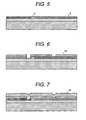
- the production process for this sensoris based on LSI production process. Firstly, as shown in Fig. 4, the monocrystal silicon substrate 1 is subjected to thermal oxidation, and a silicon oxide film 2 serving as an insulating layer is formed on the top surface of the substrate. Then polysilicon film is formed on the surface thereof by CVD method and phosphorus and other impurities are dispersed to make it electrically conductive. Then a desired form of fixed electrode 3 is obtained by the photo etching technique. Then as shown in Fig. 5, silicon oxide film 4 and silicon nitride film 5 are formed as barrier layers on the surface of the substrate according to the CVD method.
- a sacrificial layer 13consisting of phosphate glass (PSG) is formed according to the CVD method, as shown in Fig. 6.
- the thickness of this sacrificial layeris equal to the height of a desired gap (electrode gap) to be formed later.
- This sacrificial layer 13is processed by photo etching technique and desired forms of the gap 7, diaphragm substrate fixed portion 8 and etch channel 12 are obtained in one operation.
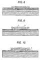
- polysilicon film 14is formed by the CVD method to the sacrificial layer 13, and is made electrically conductive with phosphorus or other impurities dispersed thereon. Then it is processed by photo etching technique to get a desired form of diaphragm 6, as shown in Fig. 8.
- part of the sacrificial layer 13is exposed to the outside from the etch channel.
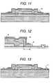
- the silicon oxide film 9is formed according to the CVD method to cover the substrate and polysilicon film 6, and is processed into a desired form by the photo etching technique. Since the gap is formed almost under vacuum, it serves as a pressure reference chamber when it is vacuum-sealed and used as an absolute pressure sensor. After that, polysilicon film 10 is formed on the oxide film 9 as surface protective film by the CVD method, as shown in Fig. 11, and is processed into a desired form by the photo etching technique.
- the sealed oxide film 9entirely with the polysilicon film 10 from the moisture-proof surface, as shown in Fig. 11.
- the distance from the end of the polysilicon film 10 to the etch channel 12is set to 10 microns. This is intended to ensure a durability of 10 years because the permeation speed of moisture is 1 microns per year according to our examination.
- silicon nitride filmcan be considered as impermeable film, but silicon nitride film has a very large film stress of about 1.5 GPa. This will cause temporal deformation of the polysilicon diaphragm 6. To avoid deformation, film thickness is set to 0.4 microns or less in this embodiment. Further, to prevent pinholes from occurring, film thickness is preferred to be 0.1 micros or more. Lastly, as shown in Fig. 13, a contact hole is opened by etching of silicon nitride film 5 and silicon oxide film 4, and photo etching is performed after sputtering of aluminum. This process provides an aluminum lead 11 of fixed electrode 3 and polysilicon movable electrode 6.
- the structure discussed aboveis characterized in that a combination of silicon oxide film manufactured by the CVD method and polysilicon film is used as a sealing material of etch channel. This simplifies the sealing structure and improves the resistance to moisture. Further, residual stresses of the oxide film and polysilicon film subsequent to formation of film are as small as about 0.15 GPa and 0.2 GPa, respectively. This reduces the temporal deformation of the diaphragm.
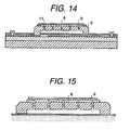
- Fig. 14is a cross sectional view representing one embodiment of a semiconductor pressure sensor.
- a holeis created on the top surface of the diaphragm 6. This hole is used as an etch channel 12, and a sacrificial layer is removed to create a pressure reference chamber.
- Polysilicon and silicon oxide filmcan be considered as a sealing material for the etch channel 12.
- the polysilicon having passed through the hole by the time hole sealing is completedis deposited on the fixed electrode to form a column, with the result that a desired gap structure cannot be obtained.
- the present embodimentadopts silicon oxide film 9 as a sealing material.
- oxide film formed by the CVD methodWhen oxide film formed by the CVD method is used, a short time is required for sealing because of a great amount of deposit on the side face of the hole, resulting in a reduced amount of deposit on the fixed electrode. As described above, however, if oxide film alone is used for sealing, moisture may permeate oxide film in the environment of high humidity to enter the gap, and may cause changes in characteristics. To solve this problem, the whole surface on oxide film is covered with polysilicon 10, similarly to the above-mentioned embodiment, or part of the oxide film is covered to ensure that the distance between the above-mentioned etch channel 9 and polysilicon 10 exceeds a certain value, with consideration given to service life and permeation speed of moisture in silicon oxide film, as shown in Fig. 15.
- Fig. 16illustrates the embodiment of the circuit integrated type pressure sensor where a signal processing circuit is integrated onto the pressure sensor.
- the pressure gageis manufactured according to the IC production process. This makes it easy to manufacture a capacitance/voltage conversion circuit consisting of the CMOS on the same substrate.
- This sensorcomprises a capacitor 21 for pressure detection, capacitor 22 for reference, oscillator 23, capacitance detecting circuit 24, computing circuit 25 for output adjustment, amplifier 26 and electrode pad 27.
- Fig. 17illustrates the structure of the capacitor 22 for reference.
- the structure of the capacitor 22 for referenceis almost the same as that of the capacitor 23 for pressure detection.
- a columnar substrate fixed portion 31is arranged within the range of the diaphragm, and the diaphragm is fragmented.
- the capacitanceis about the same as that of the capacitor for pressure detection, and capacitance value is hardly changed by pressure. So it serves as a reference capacitance in the process of detecting the capacitance to be discussed later.
- a MOS capacitor generally used as a circuit constituting componentcan be used as this capacitor 22 for reference.
- down sizing and cost cutting of the pressure sensorare achieved by integration of a pressure gage and detecting circuit. Further, a substantial improvement of measurement accuracy in capacitance detection can be realized due to reduced wiring capacitance between the capacitor and circuit.
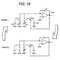
- Fig. 18illustrates a capacitance detecting circuit based on the principle of switched capacitance.
- the capacitor for pressure detection and capacitor for reference(capacitance values are assumed as Cs and Cr, respectively) are each connected with selector switches, and the states of timing 1 and timing 2 alternate.
- the capacitor for reference and capacitor for pressure detectioneach are voltage sources, and the electric charge in conformity to capacitance value is stored.
- both of themare connected to the input of the operational amplifier on the negative side. Electrical charges stored in the capacitor for reference and capacitor for pressure detection cancel each other, and the differential electrical charge flows into the operational amplifier.
- the electrical charge flowing into the operational amplifiercharges the integral capacitor Cf to change the output voltage.
- Fig. 19illustrates a the pressure sensor used as an intake pressure sensor of car engine control system: After passing through an air cleaner 41, outside air is led into the intake tube 42, and flow rate is adjusted by a throttle valve 43. Then the air is led into an intake manifold 44.
- a pressure sensor 45according to the present invention is installed in the intake manifold to detect the pressure inside the intake manifold 4. Based on the signals of this pressure sensor 45 and engine speed, an engine controller unit 49 calculates the amount of intake. It calculates the amount of fuel to be injected best suited to the amount of intake, and the calculated amount of fuel is sent to the injector 46. Gasoline injected from the injector 46 is mixed with intake air to become gas mixture. It is fed into the combustion chamber when the intake valve 48 opens, and is compressed by a piston 50. Then it is exploded and burnt by a spark plug 47.
- the hermetic structure of the pressure reference chamberis required to be very strong when consideration is given to the fact that the engine room where the pressure sensor is installed has a high temperature, the sensor is used in the highly humid environment as in the rain and the service life of the car is as long as about ten years.
- the air-tight sealed structure according to the present inventionis excellent in resistance to humidity, and sufficiently meets the above conditions.
- Fig. 20illustrates a cross sectional view
- Fig. 21shows a plan view.
- phosphorus or other impuritiesare dispersed on the top surface of the polysilicon 6, a strain gage 51 is formed on the periphery of the diaphragm in a bridge shape.
- voltageis applied to the bridge circuit and pressure is applied to the diaphragm 6, the diaphragm is bent and a change occurs to the resistance of the strain gage.
- a differential voltageoccurs according to the pressure between two output terminals of the bridge. The pressure can be measured by amplifying and reading this differential voltage.
- a sensor excellent in durabilitycan be provided by the sealed structure formed by a combination of silicon oxide film 9 formed by the above-mentioned CVD method and polysilicon film 10.
- Fig. 22is a cross sectional view of the acceleration sensor where an overhang type beam 52 for acceleration detection is installed inside a vacuum-sealed very small gap.
- the overhang type beamis a movable electrode. If the overhang type beam is deformed by acceleration, there is a change in the gap with the fixed electrode installed on the substrate in a face-to-face position. This permits the acceleration to be detected as a change in capacitance. To increase the response, the interior of the gap must be vacuum-sealed.
- a sealed structure formed by a combination of the silicon oxide film 9 according to the CVD method and polysilicon film 10is effective.
- the sealing structure of the etch channel according to the present inventionfinds application in a semiconductor vibration gyro having a vacuum sealed cavity, rotating gyro and infrared sensor.
- a chip (gage chip) type sensorconsisting of the capacitor for pressure detection and capacitance detecting circuit as described above, a 2-chip type sensor combined with a circuit chip to correct the output value, and a 1-chip type sensor with a correction circuit built in the gage chip.
- the following descriptiontakes up the example of a 2-chip type sensor: The gage chip 100 and circuit chip 101 is bonded on the lead frame comprising conductive metal formed on the resin-made sub-package 102 using the adhesive; further, each electrode pad 125 on the chip and each lead frame 105 are electrically connected by wire bonding.
- the circuit chip 101can be sealed by the cover 120 to be discussed later.
- the gage chip 100For the measurement of atmospheric pressure, the gage chip 100 must be exposed to the atmosphere through the pressure intake tube to be described later. Depending on the environment for use, dust particle, gasoline and acid may be contained in the atmosphere. When the gage chip is exposed directly to the atmosphere, the chip may be damaged. To protect the chip against them, silicone gel 104 is applied on the surface of the gage chip 100.
- the sub-package 110 with the two chips bonded with each otheris further bonded to the resin-made housing 115 having a connector 111 using adhesive and others.
- the connector 111 and circuit chipare electrically connected by aluminum wire 112.
- a cover 120 with resin-made pressure intake tube 113is bonded to seal the circuit, and this process is now complete. Adjustment is made in the following steps: Firstly, pressure application test is conducted to measure the output voltage of the gage chip. Then corrections in conformity to the characteristics are stored in the ROM installed inside the circuit chip 101. The above steps allows the sensor output to be adjusted to the specified output voltage. In the above case, a sub-package is used in the present embodiment, but need not always be used. Furthermore, the 1-chip type sensor allows the packaging costs to be cut down; for example, it permits the number of terminals to be reduced. The output of the circuit chip is output to the external signal line through the connector.
- the present embodimentuses a combination of the oxide film manufactured by the CVD method and polysilicon film as an etch channel sealing material in a pressure sensor manufactured by the sacrificial layer etching technique. This allows an etch channel sealed structure to be simplified, and prevents entry of moisture into the cavity, thereby improving moisture resistance. Moreover, sealing material with small film stress reduces temporal deformation of the diaphragm.
Landscapes
- Engineering & Computer Science (AREA)
- Microelectronics & Electronic Packaging (AREA)
- Manufacturing & Machinery (AREA)
- Physics & Mathematics (AREA)
- General Physics & Mathematics (AREA)
- Chemical & Material Sciences (AREA)
- Analytical Chemistry (AREA)
- Measuring Fluid Pressure (AREA)
- Pressure Sensors (AREA)
Description
- The present invention relates to a semiconductor sensor having a micro-cavity structure created based on the sacrificial layer etching technique, and particularly to an electrostatic capacitance semiconductor pressure detector.
- The prior art related to the present invention is disclosed in
Japanese Application Patent Announcement Publication No. Hei 08-501156 WO 94/17383 A fixed electrode 3 is formed on the surface of asilicon substrate 1 and apolysilicon diaphragm 6 is formed thereon, with agap 7 located in-between. Thisgap 7 is formed by etching and removing the sacrificial layer already formed in this area through anetch channel 12 provided on part ofpolysilicon diaphragm 6. To close thisetch channel 12 and to provide vacuum sealing of thegap 7,silicon oxide film 8 is formed to cover the whole surface of thepolysilicon diaphragm 6 and part of thesilicon substrate 1 are covered. As a result,gap 7 is formed as a vacuum sealed pressure reference chamber, and a capacitor is formed between thefixed electrode 3 provided on the substrate in the pressure reference chamber and a conductive diaphragm (movable electrode) consisting of thepolysilicon film 6. If there is a change in the external pressure, polysilicon film is displaced by differential pressure from the pressure reference chamber and a gap is changed between the two electrodes to cause a change in the capacitance of the capacitor. This change in capacitance is used to detect the pressure. - Another prior art related to the present invention is disclosed in the
Japanese Application Patent Laid-Open Publication No. Hei 11-14482 - To ensure reliability in the long-term use of the pressure sensor of the above-mentioned structure, it is necessary to reinforce the hermetic structure of the pressure reference chamber and to prevent temporal change of the output. This requires careful selection of an adequate sealing structure of the etch channel and a proper sealing material.
Japanese Application Patent Announcement Publication No. Hei 08-501156 - If the etch channel is sealed by nitride silicon film as disclosed in
Japanese Application Patent Laid-Open Publication No. Hei 11-14482 - Earlier application
EP 0 947 816 discloses a semiconductor pressure sensor of an electrostatic capacitive type in which above a substrate a moveable electrode (diaphragm) is formed. A pressure receiving surface of the diaphragm is coated with an insulation film, which is further coated with an electromagnetic shielding electric conductive film. - The present invention is intended to solve above-mentioned problems. Its object is to propose an etch channel sealing structure highly resistant to moisture and temporal change of the diaphragm in the pressure sensor produced according to the sacrificial layer etching technique, and to provide a pressure sensor characterized by excellent productivity and durability. The invention provides a pressure detector according to
claim 1. - Fig. 1 is a cross sectional view representing a first embodiment which is useful for understanding the invention;
- Fig. 2 is a plan view representing the first embodiment;
- Fig. 3 is a drawing representing how moisture passes through silicon oxide film;
- Fig. 4 is a drawing representing part of the production process in the first embodiment;
- Fig. 5 is a drawing representing part of the production process in the first embodiment;
- Fig. 6 is a drawing representing part of the production process in the first embodiment;
- Fig. 7 is a drawing representing part of the production process in the first embodiment;
- Fig. 8 is a drawing representing part of the production process in the first embodiment;
- Fig. 9 is a drawing representing part of the production process in the first embodiment;
- Fig. 10 is a drawing representing part of the production process in the first embodiment;
- Fig. 11 is a drawing representing part of the production process in the first embodiment;
- Fig. 12 is a drawing representing part of the production process in the first embodiment;
- Fig. 13 is a drawing representing part of the production process in the first embodiment,
- Fig. 14 is a cross sectional view representing a second embodiment which is useful for understanding the invention;
- Fig. 15 is a drawing representing changes in the form of polysilicon film for surface protection in the second embodiment;
- Fig. 16 is a plan view representing a third embodiment which is useful for understanding the invention;
- Fig. 17 is a cross sectional view representing a reference capacitor in the third embodiment;
- Fig. 18 is a circuit diagram representing a capacity detecting circuit in the third embodiment;
- Fig. 19 is a drawing representing the car engine control system using a semiconductor pressure sensor;
- Fig. 20 is a cross sectional view representing a fourth embodiment which is useful for understanding the invention;
- Fig. 21 is a plan view representing the fourth embodiment;
- Fig. 22 is a plan view representing a fifth embodiment of related art;
- Fig. 23 is a cross sectional view representing the pressure sensor according to the prior art;
- Fig. 24 illustrates a pressure detector according to the present invention; and
- Fig. 25 illustrates a pressure detector according to the present invention.
- The following provides a detailed description with reference to the embodiments given in the drawings: Fig. 1 is a cross sectional view representing an embodiment of a semiconductor pressure sensor, and Fig. 2 is a plan view thereof. The following describes the structure with reference to Figs. 1 and 2.
Monocrystal silicon substrate 1 is used for the substrate, andsilicon oxide film 2 is formed on the surface thereof as an insulation layer. A fixedelectrode 3 is formed on thesilicon oxide film 2, and is made of polysilicon with phosphorus or other impurities dispersed thereon.Silicon oxide film 4 is formed on fixedelectrode 3, andsilicon nitride film 5 is formed on the surface thereof in order to protect the substrate surface in the sacrificial layer etching process to be discussed later and to avoid leak current on the substrate surface.Polysilicon diaphragm 6 with part of its periphery fixed on thesilicon nitride film 5 is formed on the top of thesilicon nitride film 5, and a verysmall space 7 surrounded by the diaphragm and substrate is formed. The diaphragm substrate fixedportion 8 is annular but is fragmented at an equally spaced interval. The fragmented portion serves as anetch channel 12 leading to the gap. The etch channel is a serves as a path for etchant to enter the gap at the time of etching of the sacrificial layer to be discussed later. In order to close thisetch channel 12 and to vacuum-seal the gap, the substrate portion close to the circumference of polysilicon diaphragm 6and the surface of the outer wall of thepolysilicon diaphragm 6 are covered withsilicon oxide film 9 used for sealing. This sealing material is required to meet the following conditions: Since it must cover the substrate and movable electrode at the same time, it must be insulated to prevent leak current flowing between them. Secondly, since it covers the side wall of the diaphragm, it must provide an excellent step coverage and sealing material must not enter the inside of the gap. Thirdly, it must be of compact film in order to maintain hermeticity for a long time. Lastly, film can be formed in a short time. As a material meeting almost all of these conditions,silicon oxide film 9 formed by the CVD (chemical vapor deposition) method is adopted in the present embodiment. As shown in Fig. 3, however, the defect of sealing bysilicon oxide film 9 is that, when exposed to the environment of high temperature and high humidity for a long time, moisture may enter the gap through silicon oxide film and may change the output characteristics. To eliminate this possibility in the present embodiment, animpermeable polysilicon film 10 having a diffusion coefficient of water of 1 × 10⁻⁶ (m2/s) or less is formed on the surface of thesilicon oxide film 9, thereby preventing moisture from permeating thesilicon oxide film 9. Thispolysilicon film 10 is fixed to the ground potential made conductive by diffusion of phosphorus and other impurities, and serves as a shield against electrostatic discharge to prevent ion particle and other external electrical charge from affecting the measurement of capacity. - The following describes the principle of operations with reference to Fig. 1: The
silicon diaphragm 6 serves as a movable electrode, and forms a capacitor between it and fixedelectrode 3, with a very small gap located in-between. The interior of the gap is a vacuum pressure reference chamber, and thesilicon diaphragm 6 is deflected due to differential pressure between the pressure reference chamber and the outside. The electrode gap of the capacitor is changed by the deflection of thesilicon diaphragm 6 in response to the external pressure, and the capacitance of the capacitor is subjected to changes. This change in capacitance is detected as a change in voltage by the switched capacitor circuit, diode bridge circuit or the like. - The following describes the production method: The production process for this sensor is based on LSI production process. Firstly, as shown in Fig. 4, the
monocrystal silicon substrate 1 is subjected to thermal oxidation, and asilicon oxide film 2 serving as an insulating layer is formed on the top surface of the substrate. Then polysilicon film is formed on the surface thereof by CVD method and phosphorus and other impurities are dispersed to make it electrically conductive. Then a desired form of fixedelectrode 3 is obtained by the photo etching technique. Then as shown in Fig. 5,silicon oxide film 4 andsilicon nitride film 5 are formed as barrier layers on the surface of the substrate according to the CVD method. After that, asacrificial layer 13 consisting of phosphate glass (PSG) is formed according to the CVD method, as shown in Fig. 6. The thickness of this sacrificial layer is equal to the height of a desired gap (electrode gap) to be formed later. Thissacrificial layer 13 is processed by photo etching technique and desired forms of thegap 7, diaphragm substrate fixedportion 8 and etchchannel 12 are obtained in one operation. As shown in Fig. 7,polysilicon film 14 is formed by the CVD method to thesacrificial layer 13, and is made electrically conductive with phosphorus or other impurities dispersed thereon. Then it is processed by photo etching technique to get a desired form ofdiaphragm 6, as shown in Fig. 8. Here part of thesacrificial layer 13 is exposed to the outside from the etch channel. - When this substrate is immersed in HF based etchant, only the
sacrificial layer 13 is removed through theetch channel 12 as shown in Fig. 9, and a verysmall gap 7 is formed sandwiched between the substrate andpolysilicon film 6. Then as shown in Fig. 10, thesilicon oxide film 9 is formed according to the CVD method to cover the substrate andpolysilicon film 6, and is processed into a desired form by the photo etching technique. Since the gap is formed almost under vacuum, it serves as a pressure reference chamber when it is vacuum-sealed and used as an absolute pressure sensor. After that,polysilicon film 10 is formed on theoxide film 9 as surface protective film by the CVD method, as shown in Fig. 11, and is processed into a desired form by the photo etching technique. It is preferred cover the sealedoxide film 9 entirely with thepolysilicon film 10 from the moisture-proof surface, as shown in Fig. 11. However, there is no need of covering it entirely as shown in Fig. 12, if the distance from the end of thepolysilicon film 10 to theetch channel 12 is sufficiently long, based on the relationship between the thickness of the silicon oxide film and permeation of water shown in Fig. 3, when consideration is given to the service life and permeation speed of moisture in the oxide film. In the present embodiment, the distance from the end of thepolysilicon film 10 to theetch channel 12 is set to 10 microns. This is intended to ensure a durability of 10 years because the permeation speed of moisture is 1 microns per year according to our examination. Further, silicon nitride film can be considered as impermeable film, but silicon nitride film has a very large film stress of about 1.5 GPa. This will cause temporal deformation of thepolysilicon diaphragm 6. To avoid deformation, film thickness is set to 0.4 microns or less in this embodiment. Further, to prevent pinholes from occurring, film thickness is preferred to be 0.1 micros or more. Lastly, as shown in Fig. 13, a contact hole is opened by etching ofsilicon nitride film 5 andsilicon oxide film 4, and photo etching is performed after sputtering of aluminum. This process provides analuminum lead 11 of fixedelectrode 3 and polysiliconmovable electrode 6. - The structure discussed above is characterized in that a combination of silicon oxide film manufactured by the CVD method and polysilicon film is used as a sealing material of etch channel. This simplifies the sealing structure and improves the resistance to moisture. Further, residual stresses of the oxide film and polysilicon film subsequent to formation of film are as small as about 0.15 GPa and 0.2 GPa, respectively. This reduces the temporal deformation of the diaphragm.
- The following describes another embodiment. Fig. 14 is a cross sectional view representing one embodiment of a semiconductor pressure sensor. In this structure, a hole is created on the top surface of the
diaphragm 6. This hole is used as anetch channel 12, and a sacrificial layer is removed to create a pressure reference chamber. Polysilicon and silicon oxide film can be considered as a sealing material for theetch channel 12. In the case of polysilicon, the polysilicon having passed through the hole by the time hole sealing is completed is deposited on the fixed electrode to form a column, with the result that a desired gap structure cannot be obtained. To solve this problem, the present embodiment adoptssilicon oxide film 9 as a sealing material. When oxide film formed by the CVD method is used, a short time is required for sealing because of a great amount of deposit on the side face of the hole, resulting in a reduced amount of deposit on the fixed electrode. As described above, however, if oxide film alone is used for sealing, moisture may permeate oxide film in the environment of high humidity to enter the gap, and may cause changes in characteristics. To solve this problem, the whole surface on oxide film is covered withpolysilicon 10, similarly to the above-mentioned embodiment, or part of the oxide film is covered to ensure that the distance between the above-mentionedetch channel 9 andpolysilicon 10 exceeds a certain value, with consideration given to service life and permeation speed of moisture in silicon oxide film, as shown in Fig. 15. - With reference to Fig. 16, the following describes the embodiment of the circuit integrated type pressure sensor where a signal processing circuit is integrated onto the pressure sensor. The pressure gage is manufactured according to the IC production process. This makes it easy to manufacture a capacitance/voltage conversion circuit consisting of the CMOS on the same substrate. This sensor comprises a
capacitor 21 for pressure detection,capacitor 22 for reference,oscillator 23,capacitance detecting circuit 24,computing circuit 25 for output adjustment,amplifier 26 andelectrode pad 27. Fig. 17 illustrates the structure of thecapacitor 22 for reference. The structure of thecapacitor 22 for reference is almost the same as that of thecapacitor 23 for pressure detection. However, a columnar substrate fixedportion 31 is arranged within the range of the diaphragm, and the diaphragm is fragmented. The capacitance is about the same as that of the capacitor for pressure detection, and capacitance value is hardly changed by pressure. So it serves as a reference capacitance in the process of detecting the capacitance to be discussed later. A MOS capacitor generally used as a circuit constituting component can be used as thiscapacitor 22 for reference. In the present embodiment, down sizing and cost cutting of the pressure sensor are achieved by integration of a pressure gage and detecting circuit. Further, a substantial improvement of measurement accuracy in capacitance detection can be realized due to reduced wiring capacitance between the capacitor and circuit. - Fig. 18 illustrates a capacitance detecting circuit based on the principle of switched capacitance. The capacitor for pressure detection and capacitor for reference (capacitance values are assumed as Cs and Cr, respectively) are each connected with selector switches, and the states of
timing 1 andtiming 2 alternate. In the state oftiming 1, the capacitor for reference and capacitor for pressure detection each are voltage sources, and the electric charge in conformity to capacitance value is stored. In the state oftiming 2, both of them are connected to the input of the operational amplifier on the negative side. Electrical charges stored in the capacitor for reference and capacitor for pressure detection cancel each other, and the differential electrical charge flows into the operational amplifier. The electrical charge flowing into the operational amplifier charges the integral capacitor Cf to change the output voltage. Then when the state is shifted back to the state oftiming 1, output voltage is connected to the capacitor for pressure detection to form a feedback loop. Since a negative feedback loop is formed, the amount of electrical charge in the capacitor for pressure detection comes closer to that in the capacitor for reference every time timing 1 andtiming 2 are switched. They are kept in balance in the final stage, with the result that stable output voltage is ensured. Output voltage Vout at this time can be expressed as follows if the reference voltage is Vb:
- 1/Cs exhibits almost a linear decrease with respect to applied pressure. So Vout shows almost a linear increase with respect to applied pressure.
- Fig. 19 illustrates a the pressure sensor used as an intake pressure sensor of car engine control system: After passing through an
air cleaner 41, outside air is led into theintake tube 42, and flow rate is adjusted by athrottle valve 43. Then the air is led into anintake manifold 44. A pressure sensor 45 according to the present invention is installed in the intake manifold to detect the pressure inside theintake manifold 4. Based on the signals of this pressure sensor 45 and engine speed, anengine controller unit 49 calculates the amount of intake. It calculates the amount of fuel to be injected best suited to the amount of intake, and the calculated amount of fuel is sent to the injector 46. Gasoline injected from the injector 46 is mixed with intake air to become gas mixture. It is fed into the combustion chamber when theintake valve 48 opens, and is compressed by apiston 50. Then it is exploded and burnt by aspark plug 47. - When the pressure sensor is used for a car engine control system as in the present embodiment, the hermetic structure of the pressure reference chamber is required to be very strong when consideration is given to the fact that the engine room where the pressure sensor is installed has a high temperature, the sensor is used in the highly humid environment as in the rain and the service life of the car is as long as about ten years. The air-tight sealed structure according to the present invention is excellent in resistance to humidity, and sufficiently meets the above conditions.
- The following describes an example where a very small gap structure produced based on the present invention is applied to a piezoresistive pressure sensor. Fig. 20 illustrates a cross sectional view and Fig. 21 shows a plan view. When phosphorus or other impurities are dispersed on the top surface of the
polysilicon 6, astrain gage 51 is formed on the periphery of the diaphragm in a bridge shape. When voltage is applied to the bridge circuit and pressure is applied to thediaphragm 6, the diaphragm is bent and a change occurs to the resistance of the strain gage. A differential voltage occurs according to the pressure between two output terminals of the bridge. The pressure can be measured by amplifying and reading this differential voltage. When this sensor is used as an absolute pressure sensor, a very small gap structure must be vacuum-sealed. A sensor excellent in durability can be provided by the sealed structure formed by a combination ofsilicon oxide film 9 formed by the above-mentioned CVD method andpolysilicon film 10. - The following describes related art where a very small gap structure produced according to the present invention is applied to the capacitance type acceleration sensor: Fig. 22 is a cross sectional view of the acceleration sensor where an
overhang type beam 52 for acceleration detection is installed inside a vacuum-sealed very small gap. The overhang type beam is a movable electrode. If the overhang type beam is deformed by acceleration, there is a change in the gap with the fixed electrode installed on the substrate in a face-to-face position. This permits the acceleration to be detected as a change in capacitance. To increase the response, the interior of the gap must be vacuum-sealed. A sealed structure formed by a combination of thesilicon oxide film 9 according to the CVD method andpolysilicon film 10 is effective. - Additionally, the sealing structure of the etch channel according to the present invention finds application in a semiconductor vibration gyro having a vacuum sealed cavity, rotating gyro and infrared sensor.
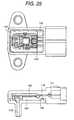
- The following describes the packaging of the pressure sensor according to the present invention with reference to Figs. 24 and 25. There are following types to get the specified pressure value; a chip (gage chip) type sensor consisting of the capacitor for pressure detection and capacitance detecting circuit as described above, a 2-chip type sensor combined with a circuit chip to correct the output value, and a 1-chip type sensor with a correction circuit built in the gage chip. The following description takes up the example of a 2-chip type sensor: The
gage chip 100 andcircuit chip 101 is bonded on the lead frame comprising conductive metal formed on the resin-made sub-package 102 using the adhesive; further, eachelectrode pad 125 on the chip and eachlead frame 105 are electrically connected by wire bonding. Thecircuit chip 101 can be sealed by thecover 120 to be discussed later. For the measurement of atmospheric pressure, thegage chip 100 must be exposed to the atmosphere through the pressure intake tube to be described later. Depending on the environment for use, dust particle, gasoline and acid may be contained in the atmosphere. When the gage chip is exposed directly to the atmosphere, the chip may be damaged. To protect the chip against them,silicone gel 104 is applied on the surface of thegage chip 100. The sub-package 110 with the two chips bonded with each other is further bonded to the resin-madehousing 115 having aconnector 111 using adhesive and others. Theconnector 111 and circuit chip are electrically connected byaluminum wire 112. In the final stage, acover 120 with resin-madepressure intake tube 113 is bonded to seal the circuit, and this process is now complete. Adjustment is made in the following steps: Firstly, pressure application test is conducted to measure the output voltage of the gage chip. Then corrections in conformity to the characteristics are stored in the ROM installed inside thecircuit chip 101. The above steps allows the sensor output to be adjusted to the specified output voltage. In the above case, a sub-package is used in the present embodiment, but need not always be used. Furthermore, the 1-chip type sensor allows the packaging costs to be cut down; for example, it permits the number of terminals to be reduced. The output of the circuit chip is output to the external signal line through the connector. - The present embodiment uses a combination of the oxide film manufactured by the CVD method
and polysilicon film as an etch channel sealing material in a pressure sensor manufactured by the sacrificial layer etching technique. This allows an etch channel sealed structure to be simplified, and prevents entry of moisture into the cavity, thereby improving moisture resistance. Moreover, sealing material with small film stress reduces temporal deformation of the diaphragm.

Claims (5)
- A pressure detector comprising;(a) a detector (100) further comprising as an integral unit;a substrate (1),a diaphragm (6) formed on said substrate by a sacrificial layer etching method,a silicon oxide film (9) provided for sealing an etchant filling hole (12) for etching the sacrificial layer, anda polysilicon film (10) covering part or whole of said silicon oxide film (9),(b) a correction circuit (101) for correction of the output of said detector;(d) a package (102, 115, 120) enclosing said correction circuit and said detector; and(d) an intake tube (113) provided in said package and used for introduction of external pressure to said detector.
- A pressure detector according to Claim 1characterized in that (h) the distance of said covered part is at least 10 microns or less from said etchant filling hole.
- A pressure detector according to Claim 1characterized in that (i) the thickness of said polysilicon film is 0.1 microns or more.
- A pressure detector according to Claim 1characterized in that (j) the thickness of said polysilicon film is between 0.1 microns and 0.4 microns.
- A pressure detector according to Claim 1 comprising;(e) a sub-package (102) further comprising said correction circuit (101) and said detector (100) as an integral unit, and having on the surface a pad connected to said correction circuit, and(f) an output terminal (125) removably connected to the external signal line and used to send a signal from said correction circuit to the external signal line;
said pressure detector furthercharacterized in that(g) said correction circuit and said detector are enclosed by said package after said pad and said output terminal are connected by a metal wire.
Applications Claiming Priority (1)
| Application Number | Priority Date | Filing Date | Title |
|---|---|---|---|
| PCT/JP1999/004485WO2001014842A1 (en) | 1999-08-20 | 1999-08-20 | Semiconductor pressure sensor and pressure sensing device |
Publications (3)
| Publication Number | Publication Date |
|---|---|
| EP1207378A1 EP1207378A1 (en) | 2002-05-22 |
| EP1207378A4 EP1207378A4 (en) | 2002-11-13 |
| EP1207378B1true EP1207378B1 (en) | 2007-08-08 |
Family
ID=14236501
Family Applications (1)
| Application Number | Title | Priority Date | Filing Date |
|---|---|---|---|
| EP99938551AExpired - LifetimeEP1207378B1 (en) | 1999-08-20 | 1999-08-20 | Semiconductor pressure sensor and pressure sensing device |
Country Status (4)
| Country | Link |
|---|---|
| US (2) | US6892582B1 (en) |
| EP (1) | EP1207378B1 (en) |
| DE (1) | DE69936794T2 (en) |
| WO (1) | WO2001014842A1 (en) |
Cited By (2)
| Publication number | Priority date | Publication date | Assignee | Title |
|---|---|---|---|---|
| EP2229967A1 (en)* | 2009-03-17 | 2010-09-22 | F. Hoffmann-La Roche AG | Cannula assembly and ambulatory infusion system with a pressure sensor made of stackes coplanar layers |
| US7816165B2 (en) | 2004-02-09 | 2010-10-19 | Analog Devices, Inc. | Method of forming a device by removing a conductive layer of a wafer |
Families Citing this family (53)
| Publication number | Priority date | Publication date | Assignee | Title |
|---|---|---|---|---|
| JP3532776B2 (en)* | 1998-10-20 | 2004-05-31 | 株式会社日立製作所 | Mounting structure for automotive sensors |
| DE10163567A1 (en)* | 2001-12-21 | 2003-07-17 | Endress & Hauser Gmbh & Co Kg | Pressure sensor with a hydrophobic coating |
| EP1394554B1 (en)* | 2002-08-30 | 2011-11-02 | STMicroelectronics Srl | Process for the fabrication of a threshold acceleration sensor |
| JP3994885B2 (en)* | 2003-02-17 | 2007-10-24 | ソニー株式会社 | MEMS element and manufacturing method thereof, diffractive MEMS element |
| FR2864341B1 (en)* | 2003-12-19 | 2006-03-24 | Commissariat Energie Atomique | HERMETIC CAVITY MICROCOMPONENT COMPRISING A PLUG AND METHOD FOR MANUFACTURING SUCH A MICROCOMPONENT |
| JP2005233877A (en)* | 2004-02-23 | 2005-09-02 | Alps Electric Co Ltd | Pressure sensor |
| US7231832B2 (en)* | 2004-09-13 | 2007-06-19 | United States Of America As Represented By The Administrator Of The National Aeronautics And Space Administration | System and method for detecting cracks and their location |
| US6968744B1 (en)* | 2004-10-18 | 2005-11-29 | Silverbrook Research Pty Ltd | Capacitative pressure sensor with close electrodes |
| US7194901B2 (en)* | 2004-10-18 | 2007-03-27 | Silverbrook Research Pty Ltd | Pressure sensor with apertured membrane guard |
| US7089798B2 (en)* | 2004-10-18 | 2006-08-15 | Silverbrook Research Pty Ltd | Pressure sensor with thin membrane |
| US7121145B2 (en)* | 2004-10-18 | 2006-10-17 | Silverbrook Research Pty Ltd | Capacitative pressure sensor |
| US7093494B2 (en)* | 2004-10-18 | 2006-08-22 | Silverbrook Research Pty Ltd | Micro-electromechanical pressure sensor |
| US7159467B2 (en)* | 2004-10-18 | 2007-01-09 | Silverbrook Research Pty Ltd | Pressure sensor with conductive ceramic membrane |
| US7089790B2 (en)* | 2004-10-18 | 2006-08-15 | Silverbrook Research Pty Ltd | Pressure sensor with laminated membrane |
| US7234357B2 (en)* | 2004-10-18 | 2007-06-26 | Silverbrook Research Pty Ltd | Wafer bonded pressure sensor |
| US7143652B2 (en)* | 2004-10-18 | 2006-12-05 | Silverbrook Research Pty Ltd | Pressure sensor for high acceleration environment |
| US7240560B2 (en)* | 2004-10-18 | 2007-07-10 | Silverbrook Research Pty Ltd | Pressure sensor with remote power source |
| US7089797B2 (en) | 2004-10-18 | 2006-08-15 | Silverbrook Research Pty Ltd | Temperature insensitive pressure sensor |
| US20080145976A1 (en)* | 2005-01-24 | 2008-06-19 | O'mahony Conor | Packaging of Micro Devices |
| US7956428B2 (en)* | 2005-08-16 | 2011-06-07 | Robert Bosch Gmbh | Microelectromechanical devices and fabrication methods |
| US7379792B2 (en) | 2005-09-29 | 2008-05-27 | Rosemount Inc. | Pressure transmitter with acoustic pressure sensor |
| US7415886B2 (en)* | 2005-12-20 | 2008-08-26 | Rosemount Inc. | Pressure sensor with deflectable diaphragm |
| JP4988217B2 (en)* | 2006-02-03 | 2012-08-01 | 株式会社日立製作所 | Method for manufacturing MEMS structure |
| DE102006008584A1 (en)* | 2006-02-24 | 2007-09-06 | Atmel Germany Gmbh | Manufacturing process for integrated piezo components |
| JP4897318B2 (en)* | 2006-03-16 | 2012-03-14 | ラピスセミコンダクタ株式会社 | Piezoresistive element and manufacturing method thereof |
| JP5127210B2 (en) | 2006-11-30 | 2013-01-23 | 株式会社日立製作所 | Semiconductor device in which MEMS sensor is embedded |
| US8358047B2 (en)* | 2008-09-29 | 2013-01-22 | Xerox Corporation | Buried traces for sealed electrostatic membrane actuators or sensors |
| US7870791B2 (en) | 2008-12-03 | 2011-01-18 | Rosemount Inc. | Method and apparatus for pressure measurement using quartz crystal |
| US8327713B2 (en) | 2008-12-03 | 2012-12-11 | Rosemount Inc. | Method and apparatus for pressure measurement using magnetic property |
| US7954383B2 (en)* | 2008-12-03 | 2011-06-07 | Rosemount Inc. | Method and apparatus for pressure measurement using fill tube |
| JP5158442B2 (en)* | 2009-02-27 | 2013-03-06 | 三菱電機株式会社 | Semiconductor pressure sensor and manufacturing method thereof |
| JP5092167B2 (en)* | 2009-03-24 | 2012-12-05 | 三菱電機株式会社 | Semiconductor pressure sensor and manufacturing method thereof |
| JP5216041B2 (en)* | 2010-04-07 | 2013-06-19 | ダイキン工業株式会社 | Transparent piezoelectric sheet with frame, each having transparent piezoelectric sheet, touch panel, and electronic device |
| US8132464B2 (en) | 2010-07-12 | 2012-03-13 | Rosemount Inc. | Differential pressure transmitter with complimentary dual absolute pressure sensors |
| US8703517B2 (en)* | 2010-10-29 | 2014-04-22 | Denso Corporation | Method of Manufacturing a Semiconductor Device Including Removing a Reformed Layer |
| DE102010062622A1 (en)* | 2010-12-08 | 2012-06-14 | Ifm Electronic Gmbh | Method for self-monitoring of a ceramic pressure measuring cell of a capacitive pressure sensor and an evaluation circuit for carrying out the method |
| DE102012200191A1 (en)* | 2012-01-09 | 2013-07-11 | Ifm Electronic Gmbh | Capacitive pressure sensor has measuring and reference capacitors that are arranged in feedback path of charge amplifier and are alternatively connected with input and output of charge amplifier |
| JP2013156066A (en)* | 2012-01-27 | 2013-08-15 | Wacom Co Ltd | Electrical capacitance pressure sensing semiconductor device |
| JP5892595B2 (en) | 2012-02-06 | 2016-03-23 | 株式会社ワコム | Position indicator |
| US8752433B2 (en) | 2012-06-19 | 2014-06-17 | Rosemount Inc. | Differential pressure transmitter with pressure sensor |
| US9200973B2 (en)* | 2012-06-28 | 2015-12-01 | Intel Corporation | Semiconductor package with air pressure sensor |
| US9429427B2 (en) | 2012-12-19 | 2016-08-30 | Intel Corporation | Inductive inertial sensor architecture and fabrication in packaging build-up layers |
| DE102013217726B4 (en) | 2013-09-05 | 2021-07-29 | Robert Bosch Gmbh | Micromechanical component for a capacitive sensor device and manufacturing method for a micromechanical component for a capacitive sensor device |
| JP6119615B2 (en) | 2014-01-08 | 2017-04-26 | 三菱電機株式会社 | Manufacturing method of semiconductor device |
| US9505607B2 (en)* | 2015-03-27 | 2016-11-29 | Intel Corporation | Methods of forming sensor integrated packages and structures formed thereby |
| US10358340B2 (en)* | 2016-04-28 | 2019-07-23 | Globalfoundries Singapore Pte. Ltd. | Integrated circuits having shielded MEMS devices and methods for fabricating shielded MEMS devices |
| JP7176986B2 (en)* | 2018-03-29 | 2022-11-22 | 旭化成株式会社 | SURFACE STRESS SENSOR, SURFACE STRESS SENSOR INSPECTION METHOD, SURFACE STRESS SENSOR MANUFACTURER |
| RU2745007C2 (en)* | 2020-03-16 | 2021-03-18 | Общество С Ограниченной Ответственностью "Оптосенс" | Diaphragm pressure sensor |
| DE102020113760B3 (en) | 2020-05-20 | 2021-11-04 | Infineon Technologies Ag | MEMS devices with support structures and related manufacturing processes |
| DE102020214757A1 (en)* | 2020-11-25 | 2022-05-25 | Robert Bosch Gesellschaft mit beschränkter Haftung | Sensor device and method for detecting an internal pressure and/or a change in the internal pressure in a gas-tight sealed internal volume of a housing component |
| US12297104B2 (en) | 2021-08-27 | 2025-05-13 | Taiwan Semiconductor Manufacturing Company Limited | Semiconductor structure and formation thereof |
| US12140489B2 (en)* | 2021-09-21 | 2024-11-12 | Invensense, Inc. | Pressure sensor with high stability |
| US12139398B2 (en)* | 2021-09-21 | 2024-11-12 | Invensense, Inc. | Pressure sensor with high stability |
Family Cites Families (10)
| Publication number | Priority date | Publication date | Assignee | Title |
|---|---|---|---|---|
| US4665610A (en)* | 1985-04-22 | 1987-05-19 | Stanford University | Method of making a semiconductor transducer having multiple level diaphragm structure |
| JP2652589B2 (en) | 1993-01-19 | 1997-09-10 | フラウンホーファー・ゲゼルシャフト ツア フェルデルンク デル アンゲワンテン フォルシュンク アインゲトラーゲナー フェライン | Pressure sensor |
| JP2991014B2 (en)* | 1993-10-08 | 1999-12-20 | 三菱電機株式会社 | Pressure sensor |
| JPH09257618A (en) | 1996-03-26 | 1997-10-03 | Toyota Central Res & Dev Lab Inc | Capacitive pressure sensor and manufacturing method thereof |
| JP3314631B2 (en) | 1996-10-09 | 2002-08-12 | 横河電機株式会社 | Vibration transducer and manufacturing method thereof |
| FR2762389B1 (en) | 1997-04-17 | 1999-05-21 | Commissariat Energie Atomique | FLEXIBLE MEMBRANE MICROSYSTEM FOR PRESSURE SENSOR AND METHOD FOR PRODUCING THE SAME |
| JPH1131825A (en) | 1997-07-10 | 1999-02-02 | Denso Corp | Method for manufacturing semiconductor dynamic quantity sensor |
| US6388279B1 (en)* | 1997-06-11 | 2002-05-14 | Denso Corporation | Semiconductor substrate manufacturing method, semiconductor pressure sensor and manufacturing method thereof |
| JP3386336B2 (en)* | 1997-06-24 | 2003-03-17 | 株式会社日立製作所 | Capacitive pressure sensor and method of manufacturing the same |
| US6167761B1 (en)* | 1998-03-31 | 2001-01-02 | Hitachi, Ltd. And Hitachi Car Engineering Co., Ltd. | Capacitance type pressure sensor with capacitive elements actuated by a diaphragm |
- 1999
- 1999-08-20EPEP99938551Apatent/EP1207378B1/ennot_activeExpired - Lifetime
- 1999-08-20USUS09/936,480patent/US6892582B1/ennot_activeExpired - Fee Related
- 1999-08-20WOPCT/JP1999/004485patent/WO2001014842A1/enactiveIP Right Grant
- 1999-08-20DEDE69936794Tpatent/DE69936794T2/ennot_activeExpired - Fee Related
- 2005
- 2005-02-04USUS11/049,872patent/US20050132814A1/ennot_activeAbandoned
Cited By (2)
| Publication number | Priority date | Publication date | Assignee | Title |
|---|---|---|---|---|
| US7816165B2 (en) | 2004-02-09 | 2010-10-19 | Analog Devices, Inc. | Method of forming a device by removing a conductive layer of a wafer |
| EP2229967A1 (en)* | 2009-03-17 | 2010-09-22 | F. Hoffmann-La Roche AG | Cannula assembly and ambulatory infusion system with a pressure sensor made of stackes coplanar layers |
Also Published As
| Publication number | Publication date |
|---|---|
| DE69936794D1 (en) | 2007-09-20 |
| EP1207378A4 (en) | 2002-11-13 |
| WO2001014842A1 (en) | 2001-03-01 |
| US20050132814A1 (en) | 2005-06-23 |
| DE69936794T2 (en) | 2008-04-30 |
| EP1207378A1 (en) | 2002-05-22 |
| US6892582B1 (en) | 2005-05-17 |
Similar Documents
| Publication | Publication Date | Title |
|---|---|---|
| EP1207378B1 (en) | Semiconductor pressure sensor and pressure sensing device | |
| US6647794B1 (en) | Absolute pressure sensor | |
| US6877383B2 (en) | Capacitive type pressure sensor | |
| EP0818046B1 (en) | Method for forming a capacitive absolute pressure sensor | |
| EP0744603B1 (en) | Linear capacitive sensor by fixing the center of a membrane | |
| JP4851011B2 (en) | Capacitive pressure sensing device with movable dielectric | |
| US7213462B2 (en) | Humidity sensor and composite sensor having humidity detecting function | |
| EP1860417A2 (en) | A pressure sensor having a chamber and a method for fabricating the same | |
| US20020109959A1 (en) | Capacitive moisture sensor and fabrication method for capacitive moisture sensor | |
| US20050067695A1 (en) | Micro-sensor | |
| US6631645B1 (en) | Semiconductor pressure sensor utilizing capacitance change | |
| JP3567094B2 (en) | Circuit built-in type sensor and pressure detecting device using the same | |
| JP2007240250A (en) | Pressure sensor, pressure sensor package, pressure sensor module, and electronic component | |
| US4459855A (en) | Semiconductor pressure sensor | |
| US20040232503A1 (en) | Semiconductor device and method of producing the same | |
| JP3310216B2 (en) | Semiconductor pressure sensor | |
| JP2007322271A (en) | Inertial force sensor and manufacturing method thereof | |
| US10422713B2 (en) | Pressure sensor suited to measuring pressure in an aggressive environment | |
| JP4539413B2 (en) | Structure of capacitive sensor | |
| JP2023070787A (en) | Inertial measurement device | |
| JPH116778A (en) | Vacuum sensor and manufacture of vacuum sensor | |
| JPH02240971A (en) | Semiconductor pressure sensor | |
| JP5251498B2 (en) | Pressure sensor | |
| JPH11258089A (en) | Semiconductor pressure sensor | |
| JPH09210825A (en) | Pressure sensor |
Legal Events
| Date | Code | Title | Description |
|---|---|---|---|
| PUAI | Public reference made under article 153(3) epc to a published international application that has entered the european phase | Free format text:ORIGINAL CODE: 0009012 | |
| 17P | Request for examination filed | Effective date:20020308 | |
| A4 | Supplementary search report drawn up and despatched | Effective date:20021002 | |
| AK | Designated contracting states | Kind code of ref document:A4 Designated state(s):AT BE CH CY DE DK ES FI FR GB GR IE IT LI LU MC NL PT SE | |
| RIC1 | Information provided on ipc code assigned before grant | Free format text:7G 01L 9/12 A, 7H 01L 29/84 B, 7G 01L 9/00 B | |
| 17Q | First examination report despatched | Effective date:20040114 | |
| RBV | Designated contracting states (corrected) | Designated state(s):DE FR GB IT | |
| GRAP | Despatch of communication of intention to grant a patent | Free format text:ORIGINAL CODE: EPIDOSNIGR1 | |
| GRAS | Grant fee paid | Free format text:ORIGINAL CODE: EPIDOSNIGR3 | |
| GRAA | (expected) grant | Free format text:ORIGINAL CODE: 0009210 | |
| RAP1 | Party data changed (applicant data changed or rights of an application transferred) | Owner name:HITACHI CAR ENGINEERING CO., LTD. Owner name:HITACHI, LTD. | |
| AK | Designated contracting states | Kind code of ref document:B1 Designated state(s):DE FR GB IT | |
| REG | Reference to a national code | Ref country code:GB Ref legal event code:FG4D | |
| REF | Corresponds to: | Ref document number:69936794 Country of ref document:DE Date of ref document:20070920 Kind code of ref document:P | |
| ET | Fr: translation filed | ||
| PLBE | No opposition filed within time limit | Free format text:ORIGINAL CODE: 0009261 | |
| STAA | Information on the status of an ep patent application or granted ep patent | Free format text:STATUS: NO OPPOSITION FILED WITHIN TIME LIMIT | |
| 26N | No opposition filed | Effective date:20080509 | |
| PGFP | Annual fee paid to national office [announced via postgrant information from national office to epo] | Ref country code:DE Payment date:20080908 Year of fee payment:10 | |
| PGFP | Annual fee paid to national office [announced via postgrant information from national office to epo] | Ref country code:FR Payment date:20080723 Year of fee payment:10 | |
| PGFP | Annual fee paid to national office [announced via postgrant information from national office to epo] | Ref country code:GB Payment date:20090728 Year of fee payment:11 | |
| PGFP | Annual fee paid to national office [announced via postgrant information from national office to epo] | Ref country code:IT Payment date:20090721 Year of fee payment:11 | |
| REG | Reference to a national code | Ref country code:FR Ref legal event code:ST Effective date:20100430 | |
| PG25 | Lapsed in a contracting state [announced via postgrant information from national office to epo] | Ref country code:FR Free format text:LAPSE BECAUSE OF NON-PAYMENT OF DUE FEES Effective date:20090831 Ref country code:DE Free format text:LAPSE BECAUSE OF NON-PAYMENT OF DUE FEES Effective date:20100302 | |
| GBPC | Gb: european patent ceased through non-payment of renewal fee | Effective date:20100820 | |
| PG25 | Lapsed in a contracting state [announced via postgrant information from national office to epo] | Ref country code:IT Free format text:LAPSE BECAUSE OF NON-PAYMENT OF DUE FEES Effective date:20100820 | |
| PG25 | Lapsed in a contracting state [announced via postgrant information from national office to epo] | Ref country code:GB Free format text:LAPSE BECAUSE OF NON-PAYMENT OF DUE FEES Effective date:20100820 |