EP1202335A2 - Method of fabricating semiconductor side wall fin - Google Patents
Method of fabricating semiconductor side wall finDownload PDFInfo
- Publication number
- EP1202335A2 EP1202335A2EP01308767AEP01308767AEP1202335A2EP 1202335 A2EP1202335 A2EP 1202335A2EP 01308767 AEP01308767 AEP 01308767AEP 01308767 AEP01308767 AEP 01308767AEP 1202335 A2EP1202335 A2EP 1202335A2
- Authority
- EP
- European Patent Office
- Prior art keywords
- gate
- fet
- channel
- drain
- source
- Prior art date
- Legal status (The legal status is an assumption and is not a legal conclusion. Google has not performed a legal analysis and makes no representation as to the accuracy of the status listed.)
- Granted
Links
- 238000004519manufacturing processMethods0.000titledescription11
- 239000004065semiconductorSubstances0.000titledescription5
- XUIMIQQOPSSXEZ-UHFFFAOYSA-NSiliconChemical compound[Si]XUIMIQQOPSSXEZ-UHFFFAOYSA-N0.000claimsdescription40
- 229910052710siliconInorganic materials0.000claimsdescription39
- 239000010703siliconSubstances0.000claimsdescription39
- 238000000034methodMethods0.000claimsdescription35
- 239000000758substrateSubstances0.000claimsdescription24
- 238000009792diffusion processMethods0.000claimsdescription15
- 238000000151depositionMethods0.000claimsdescription11
- 230000005669field effectEffects0.000claimsdescription11
- 238000005530etchingMethods0.000claimsdescription10
- 239000007943implantSubstances0.000claimsdescription9
- 239000000463materialSubstances0.000claimsdescription8
- VYPSYNLAJGMNEJ-UHFFFAOYSA-NSilicium dioxideChemical groupO=[Si]=OVYPSYNLAJGMNEJ-UHFFFAOYSA-N0.000claimsdescription6
- 229910052732germaniumInorganic materials0.000claimsdescription6
- 229910021420polycrystalline siliconInorganic materials0.000claimsdescription6
- 229920005591polysiliconPolymers0.000claimsdescription6
- 229910000676Si alloyInorganic materials0.000claimsdescription4
- OKTJSMMVPCPJKN-UHFFFAOYSA-NCarbonChemical compound[C]OKTJSMMVPCPJKN-UHFFFAOYSA-N0.000claimsdescription3
- 229910052799carbonInorganic materials0.000claimsdescription3
- GNPVGFCGXDBREM-UHFFFAOYSA-Ngermanium atomChemical compound[Ge]GNPVGFCGXDBREM-UHFFFAOYSA-N0.000claimsdescription3
- 229910021480group 4 elementInorganic materials0.000claimsdescription3
- 239000000377silicon dioxideSubstances0.000claimsdescription3
- 229910021332silicideInorganic materials0.000claimsdescription2
- FVBUAEGBCNSCDD-UHFFFAOYSA-Nsilicide(4-)Chemical compound[Si-4]FVBUAEGBCNSCDD-UHFFFAOYSA-N0.000claimsdescription2
- 235000012239silicon dioxideNutrition0.000claimsdescription2
- 239000003989dielectric materialSubstances0.000claims1
- 239000012212insulatorSubstances0.000abstractdescription5
- 239000010410layerSubstances0.000description41
- 239000010408filmSubstances0.000description19
- 125000006850spacer groupChemical group0.000description17
- 230000008021depositionEffects0.000description10
- 238000012545processingMethods0.000description10
- 239000004020conductorSubstances0.000description7
- 230000009977dual effectEffects0.000description7
- 150000004767nitridesChemical class0.000description7
- 230000015572biosynthetic processEffects0.000description6
- 238000002513implantationMethods0.000description6
- 230000003647oxidationEffects0.000description6
- 238000007254oxidation reactionMethods0.000description6
- 230000008901benefitEffects0.000description4
- 230000002950deficientEffects0.000description4
- GRYLNZFGIOXLOG-UHFFFAOYSA-NNitric acidChemical compoundO[N+]([O-])=OGRYLNZFGIOXLOG-UHFFFAOYSA-N0.000description3
- 238000005229chemical vapour depositionMethods0.000description3
- 238000007796conventional methodMethods0.000description3
- 238000002955isolationMethods0.000description3
- 229910044991metal oxideInorganic materials0.000description3
- 150000004706metal oxidesChemical class0.000description3
- 229910017604nitric acidInorganic materials0.000description3
- QTBSBXVTEAMEQO-UHFFFAOYSA-NAcetic acidChemical compoundCC(O)=OQTBSBXVTEAMEQO-UHFFFAOYSA-N0.000description2
- VHUUQVKOLVNVRT-UHFFFAOYSA-NAmmonium hydroxideChemical compound[NH4+].[OH-]VHUUQVKOLVNVRT-UHFFFAOYSA-N0.000description2
- 229910000577Silicon-germaniumInorganic materials0.000description2
- GWEVSGVZZGPLCZ-UHFFFAOYSA-NTitan oxideChemical compoundO=[Ti]=OGWEVSGVZZGPLCZ-UHFFFAOYSA-N0.000description2
- MCMNRKCIXSYSNV-UHFFFAOYSA-NZirconium dioxideChemical compoundO=[Zr]=OMCMNRKCIXSYSNV-UHFFFAOYSA-N0.000description2
- 239000002131composite materialSubstances0.000description2
- 238000010790dilutionMethods0.000description2
- 239000012895dilutionSubstances0.000description2
- 230000000694effectsEffects0.000description2
- 239000011521glassSubstances0.000description2
- 229910052751metalInorganic materials0.000description2
- 239000002184metalSubstances0.000description2
- 238000004544sputter depositionMethods0.000description2
- 239000010409thin filmSubstances0.000description2
- ZOXJGFHDIHLPTG-UHFFFAOYSA-NBoronChemical compound[B]ZOXJGFHDIHLPTG-UHFFFAOYSA-N0.000description1
- 229910017974NH40HInorganic materials0.000description1
- OAICVXFJPJFONN-UHFFFAOYSA-NPhosphorusChemical compound[P]OAICVXFJPJFONN-UHFFFAOYSA-N0.000description1
- 229910010252TiO3Inorganic materials0.000description1
- ATJFFYVFTNAWJD-UHFFFAOYSA-NTinChemical compound[Sn]ATJFFYVFTNAWJD-UHFFFAOYSA-N0.000description1
- 229910052782aluminiumInorganic materials0.000description1
- PNEYBMLMFCGWSK-UHFFFAOYSA-Naluminium oxideInorganic materials[O-2].[O-2].[O-2].[Al+3].[Al+3]PNEYBMLMFCGWSK-UHFFFAOYSA-N0.000description1
- 238000013459approachMethods0.000description1
- 229910052796boronInorganic materials0.000description1
- 238000004364calculation methodMethods0.000description1
- 230000015556catabolic processEffects0.000description1
- 238000003486chemical etchingMethods0.000description1
- 238000004140cleaningMethods0.000description1
- 229910052681coesiteInorganic materials0.000description1
- 230000000295complement effectEffects0.000description1
- 229910052593corundumInorganic materials0.000description1
- 229910052906cristobaliteInorganic materials0.000description1
- 230000007423decreaseEffects0.000description1
- 230000001419dependent effectEffects0.000description1
- 238000013461designMethods0.000description1
- 230000005684electric fieldEffects0.000description1
- 238000005516engineering processMethods0.000description1
- 229910052741iridiumInorganic materials0.000description1
- MRELNEQAGSRDBK-UHFFFAOYSA-Nlanthanum oxideInorganic materials[O-2].[O-2].[O-2].[La+3].[La+3]MRELNEQAGSRDBK-UHFFFAOYSA-N0.000description1
- 238000001459lithographyMethods0.000description1
- 230000000873masking effectEffects0.000description1
- 150000002739metalsChemical class0.000description1
- 239000000203mixtureSubstances0.000description1
- 238000005121nitridingMethods0.000description1
- KTUFCUMIWABKDW-UHFFFAOYSA-Noxo(oxolanthaniooxy)lanthanumChemical compoundO=[La]O[La]=OKTUFCUMIWABKDW-UHFFFAOYSA-N0.000description1
- 229910052698phosphorusInorganic materials0.000description1
- 239000011574phosphorusSubstances0.000description1
- 229920002120photoresistant polymerPolymers0.000description1
- 238000000623plasma-assisted chemical vapour depositionMethods0.000description1
- 229910052697platinumInorganic materials0.000description1
- 238000005498polishingMethods0.000description1
- 238000001289rapid thermal chemical vapour depositionMethods0.000description1
- 239000003870refractory metalSubstances0.000description1
- 238000011160researchMethods0.000description1
- 229910052707rutheniumInorganic materials0.000description1
- 238000004088simulationMethods0.000description1
- 239000000243solutionSubstances0.000description1
- 229910052682stishoviteInorganic materials0.000description1
- 239000002344surface layerSubstances0.000description1
- PBCFLUZVCVVTBY-UHFFFAOYSA-Ntantalum pentoxideInorganic materialsO=[Ta](=O)O[Ta](=O)=OPBCFLUZVCVVTBY-UHFFFAOYSA-N0.000description1
- 229910052905tridymiteInorganic materials0.000description1
- 238000003079width controlMethods0.000description1
- 229910001845yogo sapphireInorganic materials0.000description1
- 229910052845zirconInorganic materials0.000description1
Images


Classifications
- H—ELECTRICITY
- H10—SEMICONDUCTOR DEVICES; ELECTRIC SOLID-STATE DEVICES NOT OTHERWISE PROVIDED FOR
- H10D—INORGANIC ELECTRIC SEMICONDUCTOR DEVICES
- H10D84/00—Integrated devices formed in or on semiconductor substrates that comprise only semiconducting layers, e.g. on Si wafers or on GaAs-on-Si wafers
- H10D84/80—Integrated devices formed in or on semiconductor substrates that comprise only semiconducting layers, e.g. on Si wafers or on GaAs-on-Si wafers characterised by the integration of at least one component covered by groups H10D12/00 or H10D30/00, e.g. integration of IGFETs
- H10D84/82—Integrated devices formed in or on semiconductor substrates that comprise only semiconducting layers, e.g. on Si wafers or on GaAs-on-Si wafers characterised by the integration of at least one component covered by groups H10D12/00 or H10D30/00, e.g. integration of IGFETs of only field-effect components
- H10D84/83—Integrated devices formed in or on semiconductor substrates that comprise only semiconducting layers, e.g. on Si wafers or on GaAs-on-Si wafers characterised by the integration of at least one component covered by groups H10D12/00 or H10D30/00, e.g. integration of IGFETs of only field-effect components of only insulated-gate FETs [IGFET]
- H10D84/85—Complementary IGFETs, e.g. CMOS
- H—ELECTRICITY
- H10—SEMICONDUCTOR DEVICES; ELECTRIC SOLID-STATE DEVICES NOT OTHERWISE PROVIDED FOR
- H10D—INORGANIC ELECTRIC SEMICONDUCTOR DEVICES
- H10D30/00—Field-effect transistors [FET]
- H10D30/60—Insulated-gate field-effect transistors [IGFET]
- H10D30/62—Fin field-effect transistors [FinFET]
- H—ELECTRICITY
- H10—SEMICONDUCTOR DEVICES; ELECTRIC SOLID-STATE DEVICES NOT OTHERWISE PROVIDED FOR
- H10D—INORGANIC ELECTRIC SEMICONDUCTOR DEVICES
- H10D30/00—Field-effect transistors [FET]
- H10D30/01—Manufacture or treatment
- H10D30/021—Manufacture or treatment of FETs having insulated gates [IGFET]
- H10D30/023—Manufacture or treatment of FETs having insulated gates [IGFET] having multiple independently-addressable gate electrodes influencing the same channel
- H—ELECTRICITY
- H10—SEMICONDUCTOR DEVICES; ELECTRIC SOLID-STATE DEVICES NOT OTHERWISE PROVIDED FOR
- H10D—INORGANIC ELECTRIC SEMICONDUCTOR DEVICES
- H10D30/00—Field-effect transistors [FET]
- H10D30/01—Manufacture or treatment
- H10D30/021—Manufacture or treatment of FETs having insulated gates [IGFET]
- H10D30/024—Manufacture or treatment of FETs having insulated gates [IGFET] of fin field-effect transistors [FinFET]
- H—ELECTRICITY
- H10—SEMICONDUCTOR DEVICES; ELECTRIC SOLID-STATE DEVICES NOT OTHERWISE PROVIDED FOR
- H10D—INORGANIC ELECTRIC SEMICONDUCTOR DEVICES
- H10D30/00—Field-effect transistors [FET]
- H10D30/60—Insulated-gate field-effect transistors [IGFET]
- H10D30/67—Thin-film transistors [TFT]
- H10D30/6729—Thin-film transistors [TFT] characterised by the electrodes
- H10D30/673—Thin-film transistors [TFT] characterised by the electrodes characterised by the shapes, relative sizes or dispositions of the gate electrodes
- H—ELECTRICITY
- H10—SEMICONDUCTOR DEVICES; ELECTRIC SOLID-STATE DEVICES NOT OTHERWISE PROVIDED FOR
- H10D—INORGANIC ELECTRIC SEMICONDUCTOR DEVICES
- H10D30/00—Field-effect transistors [FET]
- H10D30/60—Insulated-gate field-effect transistors [IGFET]
- H10D30/67—Thin-film transistors [TFT]
- H10D30/674—Thin-film transistors [TFT] characterised by the active materials
- H10D30/6741—Group IV materials, e.g. germanium or silicon carbide
- H10D30/6743—Silicon
- H10D30/6744—Monocrystalline silicon
- H—ELECTRICITY
- H10—SEMICONDUCTOR DEVICES; ELECTRIC SOLID-STATE DEVICES NOT OTHERWISE PROVIDED FOR
- H10D—INORGANIC ELECTRIC SEMICONDUCTOR DEVICES
- H10D30/00—Field-effect transistors [FET]
- H10D30/60—Insulated-gate field-effect transistors [IGFET]
- H10D30/67—Thin-film transistors [TFT]
- H10D30/674—Thin-film transistors [TFT] characterised by the active materials
- H10D30/6741—Group IV materials, e.g. germanium or silicon carbide
- H10D30/6748—Group IV materials, e.g. germanium or silicon carbide having a multilayer structure or superlattice structure
- H—ELECTRICITY
- H10—SEMICONDUCTOR DEVICES; ELECTRIC SOLID-STATE DEVICES NOT OTHERWISE PROVIDED FOR
- H10D—INORGANIC ELECTRIC SEMICONDUCTOR DEVICES
- H10D86/00—Integrated devices formed in or on insulating or conducting substrates, e.g. formed in silicon-on-insulator [SOI] substrates or on stainless steel or glass substrates
- H10D86/01—Manufacture or treatment
- H—ELECTRICITY
- H10—SEMICONDUCTOR DEVICES; ELECTRIC SOLID-STATE DEVICES NOT OTHERWISE PROVIDED FOR
- H10D—INORGANIC ELECTRIC SEMICONDUCTOR DEVICES
- H10D86/00—Integrated devices formed in or on insulating or conducting substrates, e.g. formed in silicon-on-insulator [SOI] substrates or on stainless steel or glass substrates
- H10D86/201—Integrated devices formed in or on insulating or conducting substrates, e.g. formed in silicon-on-insulator [SOI] substrates or on stainless steel or glass substrates the substrates comprising an insulating layer on a semiconductor body, e.g. SOI
Definitions
- the present inventiongenerally relates to providing a dual gate metal oxide semiconductor field effect transistor (MOSFET) transistor and, more particularly, to providing a dual gate MOSFET having relatively thin epitaxially grown channels.
- MOSFETmetal oxide semiconductor field effect transistor
- Field Effect Transistor (FET) structuresmay include a single gate (a single channel) or a pair of gates, with double-gate versions providing the advantage of enabling shorter channels and thus a faster device to be produced.
- FET scalingbecomes limited by the finite depth of the gate control.
- Researchhas shown that placing gates on multiple sides of an FET channel results in improved FET performance in regard to short channel characteristics and off-current characteristics. Placing gates on multiple sides of an FET channel, provided the silicon is thin enough to be fully depleted, confines electric fields and charges much more tightly than in the standard FET in which the fields are free to penetrate deeply into an effectively infinite silicon substrate.
- the confinement possible with a fully depleted dual gate structureallows improved short channel effects and devices having gate lengths of 20 - 30 nm are possible.
- the inversion induced channelswill be formed on both sides of the silicon and possibly across the entire channel which may increase saturation current.
- Other reported benefitsinclude nearly ideal subthreshold slope, increased saturation current and reduced short-channel and floating body effects.
- Requirementsgenerally are for a thin diffusion region in the range of 5-50 nm, and gate lengths down to 20-100 nm, with the gate length preferably being two to four times the diffusion length.
- CMOSComplementary Metal Oxide Semiconductor
- Rigorous Monte Carlo device simulations and analytical calculationspredicted continual improvement in device performance down to 20-30 nm gate length, provided the silicon channel thickness can be reduced to 10-25 nm and the gate oxide thickness is reduced to 2-3 nm.
- the alignment of the top and the bottomis crucial to high performance because a mis-alignment will cause extra gate to source/drain overlap capacitance as well as loss of current drive.
- U.S. Patent 5,780,327by Chu et al. and entitled "Vertical Double-Gate Field Effect Transistor” describes a vertical double-gate field effect transistor, which includes an epitaxial channel layer and a drain layer arranged in a stack on a bulk or SOI substrate.
- the gate oxideis thermally grown on the sides of the stack using differential oxidation rates to minimize input capacitance problems.
- the gatewraps around one end of the stack, while contacts are formed on a second end.
- An etch-stop layer embedded in the second end of the stackenables contact to be made directly to the channel layer.
- U.S. Patent No. 5,773,331 by Solomon et al. and entitled "Method for Making Single and Double Gate Field Effect Transistors With Sidewall Source-Drain Contacts”describes a method for making single-gate and double-gate field effect transistors having a sidewall drain contact.
- the channel of the FETsis raised with respect to the support structure underneath and the source and drain regions form an integral part of the channel.
- U.S. Patent No. 5,757,038 by Tiwari et al. and entitled "Self-Aligned Dual Gate MOSFET with an Ultranarrow Channel”is directed to a self-aligned dual gate FET with an ultra thin channel of substantially uniform width formed by a self-aligned process. Selective etching or controlled oxidation is utilized between different materials to form a vertical channel extending between source and drain regions, having a thickness in the range from 2.5 nm to 100 nm.
- U.S. Patent No. 5,580,802 to Mayer et. al. and entitled “Silicon-on-Insulator Gate-All-Around MOSFET Fabrication Methods”describes an SOI gate-all-around (GAA) MOSFET which includes a source, channel and drain surrounded by a top gate, the latter of which also has application for other buried structures and is formed on a bottom gate dielectric which is formed on source, channel and drain semiconductor layers of an SOI wafer.
- GAAgate-all-around
- U.S. Patent No. 5,308,999 to Gotou and entitled "MOS FET Having a Thin Film SOI Structure”describes a MOS FET having a thin film SOI structure in which the breakdown voltage of an MIS (Metal Insulator Semiconductor) FET having an SOI structure is improved by forming the gate electrode on the top surface and two side surfaces of a channel region of the SOI layer and by partially extending the gate electrode toward the inside under the bottom of the channel region such that the gate electrode is not completely connected.
- MISMetal Insulator Semiconductor
- U.S. Patent No. 5,689,127 to Chu et al. and entitled "Vertical Double-Gate Field Effect Transistor”describes a vertical double-gate FET that includes a source layer, an epitaxial channel layer and a drain layer arranged in a stack on a bulk or SOI substrate.
- the gate oxideis thermally grown on the sides of the stack using differential oxidation rates to minimize input capacitance problems.
- the gatewraps around one end of the stack, while contacts are formed on a second end.
- An etch-stop layer embedded in the second end of the stackenables contact to be made directly to the channel layer.
- the lithographically defined gateis by far the simplest, but suffers from a number of disadvantages.
- definition of the gatemay leave poly spacers on the side of the diffusions or may drive a required slope on the side of the diffusion, thereby resulting in a poorer quality and/or more poorly controlled device.
- the slope of the polyinherently leads to difficulty in forming silicided gates, leading to slower device performance.
- the poly step heightposes a difficult problem for lithographic definition, as we expect steps on the order of 100 nm - 200 nm in a 50 nm design rule technology.
- Additional techniques for generating the dual-gated transistorsinclude defining the gate lithographically with high step heights (see U.S. Patent No. 4,996,574 to Shirasaki, entitled “ MIS Transistor Structure for Increasing Conductance Between Source and Drain Regions” ), forming a selective epitaxial growth which provides an "air-bridge” silicon structure (see Hon-Sum Philip Wong, International Electron Devices Meeting (IEDM) 1997, pg .427), and forming wrap-around gates with vertical carrier transport (see H. Takato IEDM, 1988, pg. 222).
- a method of forming a field effect transistor (FET) transistorcomprising the steps of forming silicon layers on a substrate. Next, epitaxial channels are formed on a side surface of the silicon layers, with one side wall of the channels therefore being exposed. The silicon layers are then removed, thereby exposing a second sidewall of the epitaxial channels. Source and drain regions are then formed, coupled to ends of the epitaxial channels. Finally, a gate is formed over the epitaxial channels.
- FETfield effect transistor
- the inventionthus seeks to provide a very thin diffusion region using a known technique for growing epitaxial regions to form the very thin channel and has the advantages of providing much tighter tolerances on channel thickness than a lithographically defined channel which can be maintained by selective etching and that epitaxial growth is not complicated by thee presence of thin confining layers.
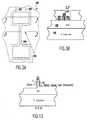
- FIG. 1Athere is shown a top view of a starting silicon-on-insulator (SOI) substrate 100.
- SOIsilicon-on-insulator
- the substrate 100is comprised of a bulk substrate 106, a buried oxide (BOX) 108 layer, and an active layer 110.
- Figures 1B and 1Calso show an oxide pad film 102 and a nitride pad film 104 on active layer 110.
- oxide pad film 102placed on top of the nitride pad film 104.
- the pad oxide 102is grown using standard oxidation techniques and would typically be in the range of 3 to 14 nm, with 8 nm being preferred.
- Pad films 104are placed upon pad oxide 102. It is preferred that nitride films be utilized as pad films 104, although other materials may also be used.
- the nitride (upper) pad films 104are typically in the range of 30 to 120 nm, with 80 nm being preferred, and define the etch areas for shallow trench isolation (STI) formation.
- STIshallow trench isolation
- the active device layer 110is patterned to form edges 112 where the silicon channel will be formed.
- the width 113 of active layer 110which is used to form what will become the channel region, is not critical, other than it must be wide enough for masking and narrow enough to confine overetching, thereby providing an adequate, practical manufacturing tolerance. It is preferred that the silicon regions that will become the source 114 and drain 116 areas and contact areas 118, 120 be formed during this stage in accordance with conventional processing techniques known to those skilled in the art.
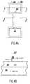
- Figures 2A, 2B and 2Ccorrespond to Figures 1A, 1B and 1C, respectively, after epitaxial growth of etch stop 202 and subsequent epitaxial growth of the channel 204.
- the etch stopis comprised of Si(0.3)Ge (0.7), and that the epitaxially grown channel be comprised of silicon or alloys of silicon with germanium and/or carbon. Alloys of silicon with other Group IV elements (particularly germanium and carbon) can be used to optimize the FET performance by adding strain to the channel and/or modifying the conduction and valence bands across the channel to alter the device threshold or improve carrier transport.
- etch stop 202 and channel 204prior to formation of etch stop 202 and channel 204, a suitable cleaning process is used to remove a portion of the silicon 110 under the oxide pad film 104.
- the width of the removed siliconshould be approximately equal to the combined width of the etch stop 202 and channel 204.
- Non-selective epitaxial deposition of etch stop 202 and channel 204may be required if faceting is excessive, although selective deposition is preferred.
- the thickness of layer 202is approximately 5 nm. Faceting will be highly dependent on details of epitaxial growth. Particularly with selective epitaxial growth, faceting may alter the thickness of the epitaxial regions as the edge of the opening is approached. Since the channel is projected to be very thin relative to the height of the growth, the area where the channel will be impacted is likely to be small. The allowed thickness before dislocations are created is sensitive to the Ge fraction and decreases quickly with increase in the Ge fraction (see A. Fischer and H. Kuhne, "Critical Dose for Strained Layer Configurations", Phys. Stat. Sol. (a), 155, 141, 1996). Then, channel 204 is epitaxially grown, preferably in the range 5-50 nm.
- the bottom and top of channel 204may be defective. Particularly if the epitaxial layer is thin, the region is likely to be extremely small and may not be significant to the formation of the device. However, if it is necessary to reove these regions, two processes are available to do so at small but tolerable, degrade of device width control. Specifically, a spacer could be deposited similar to that of spacer 302 of Figure 3B, but etched lower to uncover the top of the epitaxial region. After this spacer is formed, the buried oxide is etched underneath the spacer as shown on the left side of Figure 12. Alternatively, a thin composite spacer may be used. In this case, the bottom of the spacer are isotropically etched to uncover the top and bottom regions.
- the height of the spaceris determined by the undercut necessary to reach the epitaxial region at the bottom of the spacer, as shown on the right side of Figure 12.
- the spacersare removed selectively to the epitaxial regions and the buried oxide layer before proceeding to following processing steps. It should be noted that it is also possible to perform the procedure described above after the spacer shown in Figure 4B is removed with the spacers of the above described procedure being removed before further processing.
- Figures 3A and 3Bcorrespond to Figures 2A and 2C, respectively, after additional processing steps, as described below.
- spacers 302are formed, using a suitable technique and material widely known to those skilled in the art, to protect the channel 204 against attack.
- a maskis applied and positioned such that the mask opening 304, shown in Figure 3A, provides for removal of the exposed portion of silicon layer 110 and etch stop 202 within the mask opening 304. It is preferred that the mask 304 be aligned as closely as possible to the channel 204.
- the exposedd silicon 110 within mask opening 304is then etched using an anisotropic etch.
- the exposed silicon 110 within mask opening 304is then etched. Since not all of the silicon 110 will be removed during this etch, the silicon layer 110 is also etched laterally, stopping on etch stop 202 (see K.D. Hobart, F.J. Kub, M.E. Twigg, G.G. Jernigan, P.E. Thompson, "Ultra-Cut: A Simple Technique for the Fabrication of SOI Substrates with Ultra-thin ( ⁇ 5nm) Silicon Films", Proc. IEEE International Silicon on Insulator (SOI) Conference, p 145-146, Oct.
- KOHcan be utilized as an etchant, which has a selectivity of approximately 20:1 for Si:Si(O.3)Ge(O.7), whereas NH 4 OH is reported to have a selectivity of better than 100:1 for a 25% Ge film (see G. Wang et. al., "Highly Selective Chemical Etching of Si vs. Si(1 -x)G(x) using NH40H solution, J. Electrochem. Soc., Vol. 144(3), Mar 1997, L37).
- the expected thickness requiredis approximately 85 nm. Assuming a 20% overetch, a 100 nm etch will be required. The worst case SiGe attack would then be approximately 5 nm when KOH is utilized as the etchant, and approximately 1 nm with NH 4 OH is utilized as the etchant.
- etch stop 202is selectively etched to the channel 204.
- the selectivity for HF:H 2 O 2 :CH 3 COOHis approximately 1000:1 for a 70% Ge film. Assuming a 10 nm etch, Si attack is therefore negligible.
- the selectivity for HNO 3 :H 2 O:HF (40:20:5)is approximately 25:1 selectivity for a 50% Ge film.
- the effective HF dilutionis approximately 12:1. Oxide attack will be significant, but can be controlled in accordance with conventional processing steps widely known to those skilled in the art.
- Etch rates for HNO 3 :H 2 O:HFare approximately 40 nm/min, suggesting very short exposures, and probably allowing further dilution for control. (see D.J.
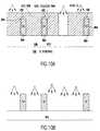
- Figures 4A and 4Bcorrespond to Figures 3A and 3B, respectively, after the etching of active layer 10 and etch stop 202. If necessary, a trim mask can be applied to remove undesired fins 402 in accordance with conventional processing techniques widely known to those skilled in the art.
- Figure 5shows the device of Figure 4A after the formation of a second channel 502 which, as will be readily recognized by those skilled in the art, can be formed by using the same processing steps as previously described to for the first channel 204.
- substrate 100may comprise many channels in addition to shown channels 204, 502 and 602.
- the substrate 100thus comprises bulk substrate 102, BOX layer 104, and channels 204, 502 and 602.
- a standard STI fill 702is provided, which is preferably a silicon dioxide layer of approximately 300 to 500 nm thick.
- a silicon dioxide layerof approximately 300 to 500 nm thick.
- other suitable materials known to those skilled in the artmay also be used as a sacrificial film.
- the STI surfaceis planarized by polishing.
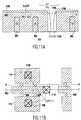
- Figure 8Ais a representational cross-sectional cut of section 1-1 of Figure 11B.
- Figure 8Ais representational because polysilicon conductor (PC) resist 802 and STI fill 702 are present during fabrication in Figure 8A, but are not present in corresponding region 141 of Figure 11B.
- PCpolysilicon conductor
- STI fill 702is selectively etched relative to pad films 104 and down to the BOX layer 108. It is preferred, but not required, that the etch also be selective relative to the BOX layer 108.
- Pad films 104are then removed selectively to the STI fill layer 702 and BOX layer 104.
- Figures 9A and 10Ashow that the pad layers 104 could be left, if desired, to allow a thin gate dielectric 904 only on the sidewalls of channels 204, 502 and 602. It is preferred that there be approximately a 10:1 selectivity in each etch, which can be accomplished with known state of the art etches. If desired, well implants may optionally be introduced at this point. These implants would be done using highly angled implants, preferably in the range of 10 to 45 degrees, with each implant rotated at approximately 90 degrees relative to each other in order to fully dope the sidewalls of the diffusion. In order to avoid doping the surface layer of the diffusions more heavily than the sides, the implantation could be done before removing the pad films 104 in the exposed areas of PC resist 802.
- Figure 8Bis a representational cross-sectional cut of section 2-2 shown in Figure 11B.
- Figure 8Bis representational because PC resist mask 802 and STI fill 702 are present during fabrication in Figure 8B, but are not shown in the region between the source 114, drain 116, and gate 902 in Figure 11B.
- Figure 8Bthus shows the selective placement of PC mask 802 during fabrication. This can be accomplished using standard pattern lithography techniques using a PC mask preferably composed of either photoresist or a hardmask.
- Figure 9Ashows the substrate of Figure 8A after gate dielectric growth 904 (e.g., SiO 2 ), and gate conductor 902 deposition.
- gate dielectric growth 904e.g., SiO 2
- gate conductor 902 depositione.g., SiO 2
- metal oxidese.g., Al 2 O 3 , ZrSiO 4 , TiO 2 , Ta 2 O 5 , ZrO 2 , etc.
- perovskitese.g., (Ba, Sr)TiO 3 , La 2 O 3
- Gate dielectric growth on each channel 204, 502 and 602could be standard furnace or single-wafer chamber oxidations in accordance with conventional methods.
- nitriding speciese.g., N 2 O, NO or N 2 implantation
- Gate dielectric deposition on each channel 204, 502 and 602can be accomplished, for example, through chemical vapor deposition (CVD) or other techniques known to those skilled in the art.
- the gate 902is deposited. Gate conductor deposition could be accomplished using conventional CVD or directional sputtering techniques. It should be understood that gate conductors other than polysilicon can also be used. For example, an SiGe mixture, refractory metals (e.g., W), metals (e.g., Ir, Al, Ru, Pt), and TiN can be used. In general, any material that can be polished and that has a high conductivity and reasonable workfunction can be used in place of polysilicon. After deposition, the gate 902 is polished in accordance with conventional techniques.
- Figure 9Bshows Figure 8B after removal of the PC resist mask 802.
- the STI surface 904is cleaned in accordance with conventional techniques.
- Figures 10A and 10Bshow extension implants to form the MOSFET device of Figure 9A after removal of STI fill 702. Implantations are done at a large angle, preferably in the range of 7 to 45 degrees, relative to a vector perpendicular to the wafer surface. Four implants, each rotated at approximately 90 degrees relative to each other about the wafer surface normal vector in order to fully dope the sidewalls of the diffusions uniformly.
- the pad oxide layer 102 on top of the diffusionsmay be utilized to avoid doping the surface of the diffusions too strongly. In this case, the pad films 104 would be removed after the implantation, but before the final implantations are done, which would follow the spacer 146 deposition.
- Figure 11Ashows the device of Figure 10A after formation of silicide layer 1102 in accordance with conventional steps. Also in accordance with conventional steps, after the gate 902 is formed, spacers 1104 are formed and the diffusions are annealed, and a layer of highly conformal dielectric fill 1106 is deposited, and then polished to the top of the gate conductor. It is preferred that dielectric fill 1106 is a nitride layer followed by a doped glass. Because of the high aspect ratios, fill properties suggest a rapid-thermal CVD or a self-sputtering deposition using a high-density plasma-enhanced CVD technique. Typically, the dielectric glass includes phosphorus and/or boron, but it can also be undoped.
- Figure 11Bshows a top view of the completed device.
- the source 114 and drain 116 regionare formed by implantation.
- Contacts 1106, 1108, 1110are added and back end of line (BEOL) processing is done in accordance with conventional steps.
- BEOLback end of line
- the second sequencecomprises the steps of removing the pad oxide 102 and pad nitride 104 films. If necessary, disposable spacers can be formed and the top of the channels 204, 502 and 602, if defective, can be etched. As shown in Figure 9A, gate oxide is then grown, and the gate 902 is deposited, preferably from among the same materials described above, and etched to form gates.
Landscapes
- Thin Film Transistor (AREA)
- Insulated Gate Type Field-Effect Transistor (AREA)
- Metal-Oxide And Bipolar Metal-Oxide Semiconductor Integrated Circuits (AREA)
- Bipolar Transistors (AREA)
- Crystals, And After-Treatments Of Crystals (AREA)
- Mechanical Treatment Of Semiconductor (AREA)
Abstract
Description
- The present invention generally relates to providing a dual gatemetal oxide semiconductor field effect transistor (MOSFET) transistor and,more particularly, to providing a dual gate MOSFET having relatively thinepitaxially grown channels.
- Field Effect Transistor (FET) structures may include a single gate (asingle channel) or a pair of gates, with double-gate versions providing theadvantage of enabling shorter channels and thus a faster device to beproduced. As gate lengths scale below 50 nm, FET scaling becomes limited bythe finite depth of the gate control. Research has shown that placinggates on multiple sides of an FET channel results in improved FETperformance in regard to short channel characteristics and off-currentcharacteristics. Placing gates on multiple sides of an FET channel,provided the silicon is thin enough to be fully depleted, confines electricfields and charges much more tightly than in the standard FET in which thefields are free to penetrate deeply into an effectively infinite siliconsubstrate. The confinement possible with a fully depleted dual gatestructure allows improved short channel effects and devices having gatelengths of 20 - 30 nm are possible. The inversion induced channels will beformed on both sides of the silicon and possibly across the entire channelwhich may increase saturation current. Other reported benefits includenearly ideal subthreshold slope, increased saturation current and reducedshort-channel and floating body effects. Requirements generally are for athin diffusion region in the range of 5-50 nm, and gate lengths down to20-100 nm, with the gate length preferably being two to four times thediffusion length.
- A number of horizontal double-gate FET structures, and particularlySOI double-gate FET structures, have been proposed. These structurestypically require a bottom gate formed beneath the thin silicon body inaddition to a conventional top gate. The fabrication of such structures isdifficult because the top and bottom gates must be aligned to a tolerancebeyond the accuracy of state of the art lithographical equipment andmethods, and because self-aligning techniques are frustrated by the layersbetween the top and bottom gates.
- In"Self-Aligned (Top and Bottom) Double-Gate MOSFET With a 25 nmThick Silicon Channel", by Hon Sum Philip et al., IEDM 97-427, IEEE 1997, adouble-gated MOSFET is considered the most promising candidate for aComplementary Metal Oxide Semiconductor (CMOS) scaled to the ultimate limitof 20-30 nm gate length. Rigorous Monte Carlo device simulations andanalytical calculations predicted continual improvement in deviceperformance down to 20-30 nm gate length, provided the silicon channelthickness can be reduced to 10-25 nm and the gate oxide thickness isreduced to 2-3 nm. However, the alignment of the top and the bottom iscrucial to high performance because a mis-alignment will cause extra gateto source/drain overlap capacitance as well as loss of current drive.
- U.S. Patent 5,780,327, by Chu et al. and entitled"VerticalDouble-Gate Field Effect Transistor" describes a vertical double-gate fieldeffect transistor, which includes an epitaxial channel layer and a drainlayer arranged in a stack on a bulk or SOI substrate. The gate oxide isthermally grown on the sides of the stack using differential oxidationrates to minimize input capacitance problems. The gate wraps around one endof the stack, while contacts are formed on a second end. An etch-stop layerembedded in the second end of the stack enables contact to be made directlyto the channel layer.
- U.S. Patent No. 5,773,331 by Solomon et al. and entitled"Method forMaking Single and Double Gate Field Effect Transistors With SidewallSource-Drain Contacts" describes a method for making single-gate anddouble-gate field effect transistors having a sidewall drain contact. Thechannel of the FETs is raised with respect to the support structureunderneath and the source and drain regions form an integral part of thechannel.
- U.S. Patent No. 5,757,038 by Tiwari et al. and entitled"Self-AlignedDual Gate MOSFET with an Ultranarrow Channel" is directed to a self-aligneddual gate FET with an ultra thin channel of substantially uniform widthformed by a self-aligned process. Selective etching or controlled oxidationis utilized between different materials to form a vertical channelextending between source and drain regions, having a thickness in the rangefrom 2.5 nm to 100 nm.
- U.S. Patent No. 5,580,802 to Mayer et. al. and entitled"Silicon-on-Insulator Gate-All-Around MOSFET Fabrication Methods" describesan SOI gate-all-around (GAA) MOSFET which includes a source, channel anddrain surrounded by a top gate, the latter of which also has applicationfor other buried structures and is formed on a bottom gate dielectric which is formed on source, channel and drain semiconductor layers of an SOIwafer.
- U.S. Patent No. 5,308,999 to Gotou and entitled "MOS FET Having aThin Film SOI Structure" describes a MOS FET having a thin film SOIstructure in which the breakdown voltage of an MIS (Metal InsulatorSemiconductor) FET having an SOI structure is improved by forming the gateelectrode on the top surface and two side surfaces of a channel region ofthe SOI layer and by partially extending the gate electrode toward theinside under the bottom of the channel region such that the gate electrodeis not completely connected.
- U.S. Patent No. 5,689,127 to Chu et al. and entitled"VerticalDouble-Gate Field Effect Transistor" describes a vertical double-gate FETthat includes a source layer, an epitaxial channel layer and a drain layerarranged in a stack on a bulk or SOI substrate. The gate oxide is thermallygrown on the sides of the stack using differential oxidation rates tominimize input capacitance problems. The gate wraps around one end of thestack, while contacts are formed on a second end. An etch-stop layerembedded in the second end of the stack enables contact to be made directlyto the channel layer.
- The lithographically defined gate is by far the simplest, but suffersfrom a number of disadvantages. First, definition of the gate may leavepoly spacers on the side of the diffusions or may drive a required slope onthe side of the diffusion, thereby resulting in a poorer quality and/ormore poorly controlled device. Second, the slope of the poly inherentlyleads to difficulty in forming silicided gates, leading to slower deviceperformance. Finally, the poly step height poses a difficult problem forlithographic definition, as we expect steps on the order of 100 nm - 200 nmin a 50 nm design rule technology.
- The key difficulties in fabricating double-gated FETs are achievingsilicidation of thin diffusions or polysilicon with acceptable contactresistance, enabling fabrication of the wraparound gate withoutmisalignment of the two gates, and fabrication of the narrow diffusions(ideally, 2-4 times smaller than the gate length).
- Additional techniques for generating the dual-gated transistorsinclude defining the gate lithographically with high step heights (see U.S.Patent No. 4,996,574 to Shirasaki, entitled "MIS Transistor Structure forIncreasing Conductance Between Source and Drain Regions"), forming aselective epitaxial growth which provides an "air-bridge" silicon structure(see Hon-Sum Philip Wong, International Electron Devices Meeting (IEDM) 1997, pg .427), and forming wrap-around gates with vertical carriertransport (see H. Takato IEDM, 1988, pg. 222).
- In summary, previous fabrication schemes have relied uponlitographically defined silicon channels and long, confined lateralepitaxial growth. However, a lithographically defined channel cannot beformed with sufficiently close tolerances and even avalable tolerancescannot be maintained adequately to support near-optimal dual gatetransistor performance in the above approaches. Further, techniques usinglateral current flow with FET widths defined laterally suffer fromdifficulty in aligning the top and bottom gates even though thickness ofsilicon can be tightly controlled.
- U. S. Patent application 09/526,857, by James W. Adkisson, John A.Bracchitta, John J. Ellis-Monaghan, Jerome B. Lasky, Kirk D. Peterson andJed H Rankin, filed on March 16, 2000, entitled "Double Planar Gated SOIMOSFET Structure" describes a method to create the double gate transistor,assuming the channel width can be made small enough.
- It is an advantage of the present invention to provide a dual gatetransistor having relatively thin epitaxially grown channels.
- According to the invention, there is provided a method of forming afield effect transistor (FET) transistor, comprising the steps of formingsilicon layers on a substrate. Next, epitaxial channels are formed on aside surface of the silicon layers, with one side wall of the channelstherefore being exposed. The silicon layers are then removed, therebyexposing a second sidewall of the epitaxial channels. Source and drainregions are then formed, coupled to ends of the epitaxial channels.Finally, a gate is formed over the epitaxial channels.
- The invention thus seeks to provide a very thin diffusion regionusing a known technique for growing epitaxial regions to form the very thinchannel and has the advantages of providing much tighter tolerances onchannel thickness than a lithographically defined channel which can bemaintained by selective etching and that epitaxial growth is notcomplicated by thee presence of thin confining layers.
- The present invention will now be described, by way of example only,with reference to preferred embodiments thereof, as illustrated in thefollowing drawings, in which:
- Figure 1A is top view of the device showing a silicon line;
- Figure 1B is a cross sectional view of cut 1-1 shown in Figure 1A;
- Figure 1C is a cross sectional view of cut 2-2 shown in Figure 1A;
- Figure 2A shows the substrate of Figure 1A after epitaxial growth ofetch stop and channel layers;
- Figure 2B is a cross sectional view of cut 1-1 shown in Figure 2A;
- Figure 2C is a cross sectional view of cut 2-2 shown in Figure 2A;
- Figure 3A shows Figure 2A with a mask opening for silicon lineremoval;
- Figure 3B shows a cross sectional view of cut 2-2 shown in Figure 3A;
- Figure 4A shows Figure 3A after the removal of any remaining portionof the silicon line and the etch stop layer;
- Figure 4B shows a cross sectional view of the 2-2 cut shown in Figure4A;
- Figure 5 shows the device of Figure 4A after the formation of asecond channel;
- Figure 6 is a representational cross section of cut 2-2 shown inFigure 5;
- Figure 7 shows the substrate of Figure 6 after shallow trenchisolation (STI) fill and polish;
- Figure 8A is a representational cross section of cut 2-2 shown inFigure 11B, after a polysilicon conductor (PC) resist mask is applied andetching;
- Figure 8B is a representational cross section of cut 2-2 shown inFigure 11B, after a PC resist mask is applied;
- Figure 9A shows the substrate of Figure 8A after gate dielectricgrowth or deposition, and gate conductor deposition;
- Figure 9B shows the substrate of Figure 8B after removal of the PCresist mask;
- Figure 10A shows removal of STI and isolation implants in thesubstrate of Figure 9A;
- Figure 10B shows extension implants in the substrate of Figure 9B;
- Figure 11A shows the completed device of Figure 10A before contacts;
- Figure 11B shows a top view of the completed device, and
- Figure 12 illustrates a technique of removing defective material dueto excessive faceting.
- Referring now to Figure 1A, there is shown a top view of a startingsilicon-on-insulator (SOI)
substrate 100. As shown in Figures 1B and 1C,which correspond to sections 1-1 and 2-2 shown in Figure 1A, respectively,thesubstrate 100 is comprised of abulk substrate 106, a buried oxide(BOX) 108 layer, and anactive layer 110. Figures 1B and 1C also show anoxide pad film 102 and anitride pad film 104 onactive layer 110. Thoseskilled in the art will realize that it may be preferable to have theoxidepad film 102 placed on top of thenitride pad film 104. Thepad oxide 102is grown using standard oxidation techniques and would typically be in therange of 3 to 14 nm, with 8 nm being preferred.Pad films 104 are placeduponpad oxide 102. It is preferred that nitride films be utilized aspadfilms 104, although other materials may also be used. The nitride (upper)pad films 104 are typically in the range of 30 to 120 nm, with 80 nm beingpreferred, and define the etch areas for shallow trench isolation (STI)formation. - The
active device layer 110 is patterned to formedges 112 where thesilicon channel will be formed. Thewidth 113 ofactive layer 110, which isused to form what will become the channel region, is not critical, otherthan it must be wide enough for masking and narrow enough to confine overetching, thereby providing an adequate, practical manufacturingtolerance. It is preferred that the silicon regions that will become thesource 114 and drain 116 areas andcontact areas - Figures 2A, 2B and 2C correspond to Figures 1A, 1B and 1C,respectively, after epitaxial growth of
etch stop 202 and subsequentepitaxial growth of thechannel 204. Preferably, the etch stop is comprisedof Si(0.3)Ge (0.7), and that the epitaxially grown channel be comprised ofsilicon or alloys of silicon with germanium and/or carbon. Alloys ofsilicon with other Group IV elements (particularly germanium and carbon)can be used to optimize the FET performance by adding strain to the channeland/or modifying the conduction and valence bands across the channel toalter the device threshold or improve carrier transport. It will beevident to those skilled in the art that, prior to formation ofetch stop 202 andchannel 204, a suitable cleaning process is used to remove aportion of thesilicon 110 under theoxide pad film 104. The width of theremoved silicon should be approximately equal to the combined width of theetch stop 202 andchannel 204. - Non-selective epitaxial deposition of
etch stop 202 andchannel 204may be required if faceting is excessive, although selective deposition ispreferred. Preferably, the thickness oflayer 202 is approximately 5 nm.Faceting will be highly dependent on details of epitaxial growth.Particularly with selective epitaxial growth, faceting may alter thethickness of the epitaxial regions as the edge of the opening isapproached. Since the channel is projected to be very thin relative to theheight of the growth, the area where the channel will be impacted is likelyto be small. The allowed thickness before dislocations are created issensitive to the Ge fraction and decreases quickly with increase in the Gefraction (see A. Fischer and H. Kuhne, "Critical Dose for Strained LayerConfigurations", Phys. Stat. Sol. (a), 155, 141, 1996). Then,channel 204is epitaxially grown, preferably in the range 5-50 nm. - The bottom and top of
channel 204 may be defective. Particularly ifthe epitaxial layer is thin, the region is likely to be extremely small andmay not be significant to the formation of the device. However, if it isnecessary to reove these regions, two processes are available to do so atsmall but tolerable, degrade of device width control. Specifically, aspacer could be deposited similar to that ofspacer 302 of Figure 3B, butetched lower to uncover the top of the epitaxial region. After this spaceris formed, the buried oxide is etched underneath the spacer as shown on theleft side of Figure 12. Alternatively, a thin composite spacer may be used. In this case, the bottom of the spacer are isotropically etched touncover the top and bottom regions. The height of the spacer (overetch) isdetermined by the undercut necessary to reach the epitaxial region at thebottom of the spacer, as shown on the right side of Figure 12. After thedefective regions are etched, the spacers are removed selectively to theepitaxial regions and the buried oxide layer before proceeding to followingprocessing steps. It should be noted that it is also possible to performthe procedure described above after the spacer shown in Figure 4B isremoved with the spacers of the above described procedure being removedbefore further processing. - Figures 3A and 3B correspond to Figures 2A and 2C, respectively,after additional processing steps, as described below. As shown in Figure3B,
spacers 302 are formed, using a suitable technique and material widelyknown to those skilled in the art, to protect thechannel 204 againstattack. - Then, a mask is applied and positioned such that the
mask opening 304, shown in Figure 3A, provides for removal of the exposed portion ofsilicon layer 110 and etch stop 202 within themask opening 304. It ispreferred that themask 304 be aligned as closely as possible to thechannel 204. Theexposedd silicon 110 withinmask opening 304 is thenetched using an anisotropic etch. - The exposed
silicon 110 withinmask opening 304 is then etched. Sincenot all of thesilicon 110 will be removed during this etch, thesiliconlayer 110 is also etched laterally, stopping on etch stop 202 (see K.D.Hobart, F.J. Kub, M.E. Twigg, G.G. Jernigan, P.E. Thompson, "Ultra-Cut: ASimple Technique for the Fabrication of SOI Substrates with Ultra-thin(<5nm) Silicon Films", Proc. IEEE International Silicon on Insulator (SOI)Conference, p 145-146, Oct. 1988.) KOH can be utilized as an etchant, whichhas a selectivity of approximately 20:1 for Si:Si(O.3)Ge(O.7), whereasNH4OH is reported to have a selectivity of better than 100:1 for a 25% Gefilm (see G. Wang et. al., "Highly Selective Chemical Etching of Si vs.Si(1 -x)G(x) using NH40H solution, J. Electrochem. Soc., Vol. 144(3), Mar1997, L37). - Thus, with an overlay of approximately 70 nm, and an edge toleranceof approximately 20 nm, the expected thickness required is approximately 85nm. Assuming a 20% overetch, a 100 nm etch will be required. The worst caseSiGe attack would then be approximately 5 nm when KOH is utilized as theetchant, and approximately 1 nm with NH4OH is utilized as the etchant.
- Next, etch stop 202 is selectively etched to the
channel 204. Theselectivity for HF:H2O2:CH3COOH is approximately 1000:1 for a 70% Ge film.Assuming a 10 nm etch, Si attack is therefore negligible. The selectivityfor HNO3:H2O:HF (40:20:5) is approximately 25:1 selectivity for a 50% Gefilm. The effective HF dilution is approximately 12:1. Oxide attack will besignificant, but can be controlled in accordance with conventionalprocessing steps widely known to those skilled in the art. Etch rates forHNO3:H2O:HF are approximately 40 nm/min, suggesting very short exposures,and probably allowing further dilution for control. (see D.J. Godbey et.al., "Selective Removal of Si(1 -x)Ge(x) from <100> Si using HNO3 and HF,J. Electrochem. Soc., 139(10), 2943, 1992).Spacers 302 can be removed, ifnecessary, in accordance with conventional processing steps widely known tothose skilled in the art. - Figures 4A and 4B correspond to Figures 3A and 3B, respectively,after the etching of active layer 10 and
etch stop 202. If necessary, atrim mask can be applied to removeundesired fins 402 in accordance withconventional processing techniques widely known to those skilled in theart. Figure 5 shows the device of Figure 4A after the formation of asecondchannel 502 which, as will be readily recognized by those skilled in theart, can be formed by using the same processing steps as previouslydescribed to for thefirst channel 204. - Having formed the first 204 and second 502 channel regions, a firstsequence of final processing steps required to complete the dual-gatedtransistor is described below.
- Referring now to Figure 6,
channels additional channel 602 that may be used to formanother gate structure. It should thus be understood by those skilled inthe art thatsubstrate 100 may comprise many channels in addition to shownchannels substrate 100 thus comprisesbulksubstrate 102,BOX layer 104, andchannels - Then, in Figure 7, a standard STI fill 702 is provided, which ispreferably a silicon dioxide layer of approximately 300 to 500 nm thick.However, other suitable materials known to those skilled in the art mayalso be used as a sacrificial film. Preferably, the STI surface isplanarized by polishing.
- Figure 8A is a representational cross-sectional cut of section 1-1 ofFigure 11B. Figure 8A is representational because polysilicon conductor(PC) resist 802 and STI fill 702 are present during fabrication in Figure8A, but are not present in corresponding region 141 of Figure 11B. Afterplacing the PC resist
mask 802 on a selected regions of STI fill 702, STI fill 702 is selectively etched relative to padfilms 104 and down to theBOX layer 108. It is preferred, but not required, that the etch also beselective relative to theBOX layer 108.Pad films 104 are then removedselectively to theSTI fill layer 702 andBOX layer 104. Figures 9A and 10Ashow that the pad layers 104 could be left, if desired, to allow a thingate dielectric 904 only on the sidewalls ofchannels pad films 104 in the exposed areas of PC resist 802. - Figure 8B is a representational cross-sectional cut of section 2-2shown in Figure 11B. Figure 8B is representational because PC resist
mask 802 and STI fill 702 are present during fabrication in Figure 8B, but arenot shown in the region between thesource 114, drain 116, andgate 902 inFigure 11B. Figure 8B thus shows the selective placement ofPC mask 802during fabrication. This can be accomplished using standard patternlithography techniques using a PC mask preferably composed of eitherphotoresist or a hardmask. - Figure 9A shows the substrate of Figure 8A after gate dielectricgrowth 904 (e.g., SiO2), and
gate conductor 902 deposition. It should beunderstood that nitrided oxides, nitride/oxide composites, metal oxides(e.g., Al2O3, ZrSiO4, TiO2, Ta2O5, ZrO2, etc.), perovskites (e.g., (Ba,Sr)TiO3, La2O3) and combinations of the above can also be used as thedielectric. Gate dielectric growth on eachchannel channel - After etching, the
gate 902 is deposited. Gate conductor depositioncould be accomplished using conventional CVD or directional sputteringtechniques. It should be understood that gate conductors other thanpolysilicon can also be used. For example, an SiGe mixture, refractorymetals (e.g., W), metals (e.g., Ir, Al, Ru, Pt), and TiN can be used. Ingeneral, any material that can be polished and that has a high conductivity and reasonable workfunction can be used in place of polysilicon. Afterdeposition, thegate 902 is polished in accordance with conventionaltechniques. - Figure 9B shows Figure 8B after removal of the PC resist
mask 802.TheSTI surface 904 is cleaned in accordance with conventional techniques. - Figures 10A and 10B show extension implants to form the MOSFET deviceof Figure 9A after removal of STI fill 702. Implantations are done at alarge angle, preferably in the range of 7 to 45 degrees, relative to avector perpendicular to the wafer surface. Four implants, each rotated atapproximately 90 degrees relative to each other about the wafer surfacenormal vector in order to fully dope the sidewalls of the diffusionsuniformly. The
pad oxide layer 102 on top of the diffusions may be utilizedto avoid doping the surface of the diffusions too strongly. In this case,thepad films 104 would be removed after the implantation, but before thefinal implantations are done, which would follow the spacer 146 deposition. - Figure 11A shows the device of Figure 10A after formation of
silicidelayer 1102 in accordance with conventional steps. Also in accordance withconventional steps, after thegate 902 is formed,spacers 1104 are formedand the diffusions are annealed, and a layer of highly conformaldielectricfill 1106 is deposited, and then polished to the top of the gate conductor.It is preferred thatdielectric fill 1106 is a nitride layer followed by adoped glass. Because of the high aspect ratios, fill properties suggest arapid-thermal CVD or a self-sputtering deposition using a high-densityplasma-enhanced CVD technique. Typically, the dielectric glass includesphosphorus and/or boron, but it can also be undoped. - Figure 11B shows a top view of the completed device. The
source 114and drain 116 region are formed by implantation.Contacts - Referring again to Figure 8A, the second sequence comprises the stepsof removing the
pad oxide 102 andpad nitride 104 films. If necessary,disposable spacers can be formed and the top of thechannels gate 902 is deposited, preferably from among the samematerials described above, and etched to form gates.
Claims (22)
- A field effect transistor (FET) comprising:a substrate;a source region and a drain region in the substrate, each of saidsource region and said drain region having a top, bottom and at least twoside diffusion surfaces, the source and drain regions separated by anepitaxially grown channel region having a top, bottom and side channelsurfaces substantially coplanar with corresponding ones of the diffusionsurfaces;a gate adjacent the top and the side channel surfaces andelectrically insulated from the top and side channel surfaces; andthe gate comprising a planar top surface, the planar top surfacehaving a contact for receiving a gate control voltage for controlling theFET.
- The FET as claimed in claim 1, in which the source and drain have acontact for receiving a control voltage for controlling the FET.
- The FET as claimed in claim 1 or claim 2, in which the gate issubstantially centered between and substantially parallel to said sourceregion and said drain region.
- The FET as claimed in any preceding claim, further comprising asilicide layer that contacts a top surface of said gate.
- The FET as claimed in any preceding claim, further comprising adielectric layer that contacts a first side end and a second side end ofsaid gate.
- The FET as claimed in any preceding claim, further comprising adielectric that contacts side surfaces of the channels.
- The FET as claimed in any preceding claim, where the gate iscomprised of polysilicon.
- The FET as claimed in any preceding claim, in which the channel isapproximately one fourth of a length of the FET.
- The FET as claimed in any preceding claim, further comprising adielectric material in the gate for electrically separating the gate intotwo electrically isolated portions, each having a substantially coplanartop surface and a contact pad on each respective substantially coplanar topsurface.
- The FET as claimed in any preceding claim, in which said epitaxialchannel is formed of a combination of Group IV elements.
- The FET as claimed in any of claims 1 to 9, in which said epitaxialchannel is formed of an alloy of silicon and a Group IV element.
- The FET as claimed in any of claims 1 to 9, in which said epitaxialchannel is formed of an alloy of silicon and at least one of germanium andcarbon.
- A method of forming a field effect transistor (FET) transistor,comprising:providing a substrate;forming a layer on the substrate, the layer having a side surface;forming an epitaxial channel on the side surface, the channel havinga first sidewall;removing the layer for exposing a second sidewall of the channel;forming source and drain regions coupled to ends of the firstchannel; andforming a gate adjacent to at least one of the sidewalls of thechannel.
- A method for forming a double gated field effect transistor (FET),comprising the steps of:forming on a substrate a first and a second epitaxially grownchannels;etching areas within a silicon layer to form a source and a drain,wherein a side surface of the source and the drain contact opposing endsurfaces of the first and second epitaxially grown channels; andforming a gate that contacts a top surface and two side surfaces ofthe first and second epitaxially grown channels and a top surface of thesubstrate.
- The method as claimed in claim 14, in which the forming stepcomprises the steps of:forming first and second silicon lines, each end of the silicon linescontact an end of the source and the drain;forming an etch stop layer on an exposed side surface of each of thefirst and second silicon lines;epitaxially growing first and second silicon layers on each etch stoplayer;etching away the first and second silicon lines and etch stop layers;filling areas surrounding the first and second epitaxially grownsilicon layers and between the source and the drain with an oxide fill;etching a portion of the oxide fill to form an area that defines agate, wherein the area that defines the gate is substantially centeredbetween and substantially parallel to the source and the drain; anddepositing a material to form a gate.
- The method as claimed in claim 15, further comprising the steps of:etching the oxide fill between the gate the source to expose thefirst and second epitaxially grown silicon layers; andetching the oxide fill between the gate and the drain to expose thefirst and second epitaxially grown silicon layers.
- The method as claimed in claim 15 or claim 16, further comprising thestep of forming an oxide on the first and second epitaxially grown siliconlayers.
- The method as claimed in claim 17, in which the oxide is silicondioxide.
- The method as claimed in any of claims 16 to 18, further comprisingthe steps of:implanting a portion of the epitaxially grown silicon layers betweenthe gate and the source; andimplanting a portion of the epitaxially grown silicon layers betweenthe gate and the drain.
- The method as claimed in claim 19, in which the implanting step is inthe range of 10 to 45 degrees relative to a vector perpendicular to a topsurface of the epitaxially grown silicon layers.
- The method as claimed in claim 19 or claim 20, in which the implantsare done in a series at approximately 90 degrees relative to each other.
- The method as claimed in any of claims 14 to 21, further comprisingthe step of forming a contact on each of the gate, the source and thedrain.
Applications Claiming Priority (2)
| Application Number | Priority Date | Filing Date | Title |
|---|---|---|---|
| US691353 | 1996-08-02 | ||
| US09/691,353US7163864B1 (en) | 2000-10-18 | 2000-10-18 | Method of fabricating semiconductor side wall fin |
Publications (3)
| Publication Number | Publication Date |
|---|---|
| EP1202335A2true EP1202335A2 (en) | 2002-05-02 |
| EP1202335A3 EP1202335A3 (en) | 2004-09-08 |
| EP1202335B1 EP1202335B1 (en) | 2009-03-18 |
Family
ID=24776208
Family Applications (1)
| Application Number | Title | Priority Date | Filing Date |
|---|---|---|---|
| EP01308767AExpired - LifetimeEP1202335B1 (en) | 2000-10-18 | 2001-10-15 | Method of fabricating semiconductor side wall fin |
Country Status (9)
| Country | Link |
|---|---|
| US (3) | US7163864B1 (en) |
| EP (1) | EP1202335B1 (en) |
| JP (1) | JP4071951B2 (en) |
| KR (1) | KR100444095B1 (en) |
| CN (1) | CN100530567C (en) |
| AT (1) | ATE426246T1 (en) |
| DE (1) | DE60138000D1 (en) |
| SG (1) | SG97204A1 (en) |
| TW (1) | TW526564B (en) |
Cited By (39)
| Publication number | Priority date | Publication date | Assignee | Title |
|---|---|---|---|---|
| WO2004032246A1 (en)* | 2002-09-30 | 2004-04-15 | Advanced Micro Devices, Inc. | Finfet having improved carrier mobility and method of its formation |
| WO2004068585A1 (en)* | 2003-01-23 | 2004-08-12 | Advanced Micro Devices, Inc. | Strained channel finfet |
| WO2004068589A1 (en)* | 2003-01-23 | 2004-08-12 | Advanced Micro Devices, Inc. | Narrow fin finfet |
| WO2004073044A3 (en)* | 2003-02-13 | 2004-12-02 | Massachusetts Inst Technology | Finfet device and method to make same |
| US6852576B2 (en) | 2003-04-03 | 2005-02-08 | Advanced Micro Devices, Inc. | Method for forming structures in finfet devices |
| WO2005098963A1 (en)* | 2004-03-31 | 2005-10-20 | Intel Corporation | A bulk non-planar transistor having a strained channel with enhanced mobility and methods of fabrication |
| US7005366B2 (en) | 2002-08-23 | 2006-02-28 | Intel Corporation | Tri-gate devices and methods of fabrication |
| US7029958B2 (en) | 2003-11-04 | 2006-04-18 | Advanced Micro Devices, Inc. | Self aligned damascene gate |
| US7042009B2 (en) | 2004-06-30 | 2006-05-09 | Intel Corporation | High mobility tri-gate devices and methods of fabrication |
| US7105390B2 (en) | 2003-12-30 | 2006-09-12 | Intel Corporation | Nonplanar transistors with metal gate electrodes |
| US7193279B2 (en) | 2005-01-18 | 2007-03-20 | Intel Corporation | Non-planar MOS structure with a strained channel region |
| EP1644988A4 (en)* | 2003-06-25 | 2007-04-11 | Ibm | HIGH DENSITY FINFETS INTEGRATION PROJECT |
| US7241653B2 (en) | 2003-06-27 | 2007-07-10 | Intel Corporation | Nonplanar device with stress incorporation layer and method of fabrication |
| US7268058B2 (en) | 2004-01-16 | 2007-09-11 | Intel Corporation | Tri-gate transistors and methods to fabricate same |
| US7279375B2 (en) | 2005-06-30 | 2007-10-09 | Intel Corporation | Block contact architectures for nanoscale channel transistors |
| US7326656B2 (en) | 2004-09-30 | 2008-02-05 | Intel Corporation | Method of forming a metal oxide dielectric |
| EP1892765A1 (en)* | 2006-08-23 | 2008-02-27 | INTERUNIVERSITAIR MICROELEKTRONICA CENTRUM vzw (IMEC) | Method for doping a fin-based semiconductor device |
| US7348284B2 (en) | 2004-08-10 | 2008-03-25 | Intel Corporation | Non-planar pMOS structure with a strained channel region and an integrated strained CMOS flow |
| US7396711B2 (en) | 2005-12-27 | 2008-07-08 | Intel Corporation | Method of fabricating a multi-cornered film |
| US7402875B2 (en) | 2005-08-17 | 2008-07-22 | Intel Corporation | Lateral undercut of metal gate in SOI device |
| US7432557B1 (en) | 2003-07-08 | 2008-10-07 | Advanced Micro Devices, Inc. | FinFET device with multiple channels |
| US7449373B2 (en) | 2006-03-31 | 2008-11-11 | Intel Corporation | Method of ion implanting for tri-gate devices |
| US7498225B1 (en) | 2003-12-04 | 2009-03-03 | Advanced Micro Devices, Inc. | Systems and methods for forming multiple fin structures using metal-induced-crystallization |
| US7518196B2 (en) | 2005-02-23 | 2009-04-14 | Intel Corporation | Field effect transistor with narrow bandgap source and drain regions and method of fabrication |
| US7547637B2 (en) | 2005-06-21 | 2009-06-16 | Intel Corporation | Methods for patterning a semiconductor film |
| US7550333B2 (en) | 2004-10-25 | 2009-06-23 | Intel Corporation | Nonplanar device with thinned lower body portion and method of fabrication |
| US7579280B2 (en) | 2004-06-01 | 2009-08-25 | Intel Corporation | Method of patterning a film |
| US7670928B2 (en) | 2006-06-14 | 2010-03-02 | Intel Corporation | Ultra-thin oxide bonding for S1 to S1 dual orientation bonding |
| US7679134B1 (en) | 2002-11-26 | 2010-03-16 | Globalfoundries | FinFET device with multiple fin structures |
| US7692246B2 (en) | 2006-01-12 | 2010-04-06 | Infineon Technologies Ag | Production method for a FinFET transistor arrangement, and corresponding FinFET transistor arrangement |
| EP1916717A3 (en)* | 2006-08-23 | 2010-12-22 | Imec | Method for doping a fin-based semiconductor device |
| US7859053B2 (en) | 2004-09-29 | 2010-12-28 | Intel Corporation | Independently accessed double-gate and tri-gate transistors in same process flow |
| US7858481B2 (en) | 2005-06-15 | 2010-12-28 | Intel Corporation | Method for fabricating transistor with thinned channel |
| US7902598B2 (en) | 2005-06-24 | 2011-03-08 | Micron Technology, Inc. | Two-sided surround access transistor for a 4.5F2 DRAM cell |
| US7902014B2 (en) | 2005-09-28 | 2011-03-08 | Intel Corporation | CMOS devices with a single work function gate electrode and method of fabrication |
| US7915167B2 (en) | 2004-09-29 | 2011-03-29 | Intel Corporation | Fabrication of channel wraparound gate structure for field-effect transistor |
| US8362566B2 (en) | 2008-06-23 | 2013-01-29 | Intel Corporation | Stress in trigate devices using complimentary gate fill materials |
| US9704859B1 (en) | 2016-05-06 | 2017-07-11 | International Business Machines Corporation | Forming semiconductor fins with self-aligned patterning |
| US10157745B2 (en) | 2016-06-29 | 2018-12-18 | International Business Machines Corporation | High aspect ratio gates |
Families Citing this family (66)
| Publication number | Priority date | Publication date | Assignee | Title |
|---|---|---|---|---|
| JP4546021B2 (en)* | 2002-10-02 | 2010-09-15 | ルネサスエレクトロニクス株式会社 | Insulated gate field effect transistor and semiconductor device |
| KR100474850B1 (en)* | 2002-11-15 | 2005-03-11 | 삼성전자주식회사 | Silicon/Oxide/Nitride/Oxide/Silicon nonvolatile memory with vertical channel and Fabricating method thereof |
| US6720619B1 (en)* | 2002-12-13 | 2004-04-13 | Taiwan Semiconductor Manufacturing Company, Ltd. | Semiconductor-on-insulator chip incorporating partially-depleted, fully-depleted, and multiple-gate devices |
| KR100483425B1 (en)* | 2003-03-17 | 2005-04-14 | 삼성전자주식회사 | Semiconductor device and method for manufacturing the same |
| JP4632046B2 (en)* | 2003-04-09 | 2011-02-16 | 日本電気株式会社 | Vertical MISFET semiconductor device having high mobility silicon channel |
| US7074656B2 (en)* | 2003-04-29 | 2006-07-11 | Taiwan Semiconductor Manufacturing Company, Ltd. | Doping of semiconductor fin devices |
| US6909186B2 (en)* | 2003-05-01 | 2005-06-21 | International Business Machines Corporation | High performance FET devices and methods therefor |
| JP4105044B2 (en) | 2003-06-13 | 2008-06-18 | 株式会社東芝 | Field effect transistor |
| US7456476B2 (en) | 2003-06-27 | 2008-11-25 | Intel Corporation | Nonplanar semiconductor device with partially or fully wrapped around gate electrode and methods of fabrication |
| KR100973092B1 (en) | 2003-07-21 | 2010-07-29 | 매그나칩 반도체 유한회사 | Fabrication method of vertical MOS capacitor using silicon on insulator wafer |
| US7013447B2 (en)* | 2003-07-22 | 2006-03-14 | Freescale Semiconductor, Inc. | Method for converting a planar transistor design to a vertical double gate transistor design |
| US7355253B2 (en) | 2003-08-22 | 2008-04-08 | International Business Machines Corporation | Strained-channel Fin field effect transistor (FET) with a uniform channel thickness and separate gates |
| US6946377B2 (en)* | 2003-10-29 | 2005-09-20 | Texas Instruments Incorporated | Multiple-gate MOSFET device with lithography independent silicon body thickness and methods for fabricating the same |
| US7388258B2 (en)* | 2003-12-10 | 2008-06-17 | International Business Machines Corporation | Sectional field effect devices |
| US7115920B2 (en)* | 2004-04-12 | 2006-10-03 | International Business Machines Corporation | FinFET transistor and circuit |
| KR100555573B1 (en) | 2004-09-10 | 2006-03-03 | 삼성전자주식회사 | Semiconductor device having a junction region extended by SEB film and method for manufacturing same |
| JP2008529295A (en)* | 2005-01-28 | 2008-07-31 | エヌエックスピー ビー ヴィ | Method for manufacturing a dual gate FET |
| US20060202266A1 (en) | 2005-03-14 | 2006-09-14 | Marko Radosavljevic | Field effect transistor with metal source/drain regions |
| JP4987244B2 (en)* | 2005-04-28 | 2012-07-25 | 株式会社東芝 | Manufacturing method of semiconductor device |
| US9153645B2 (en) | 2005-05-17 | 2015-10-06 | Taiwan Semiconductor Manufacturing Company, Ltd. | Lattice-mismatched semiconductor structures with reduced dislocation defect densities and related methods for device fabrication |
| US8324660B2 (en) | 2005-05-17 | 2012-12-04 | Taiwan Semiconductor Manufacturing Company, Ltd. | Lattice-mismatched semiconductor structures with reduced dislocation defect densities and related methods for device fabrication |
| US7339241B2 (en)* | 2005-08-31 | 2008-03-04 | Freescale Semiconductor, Inc. | FinFET structure with contacts |
| US7479421B2 (en) | 2005-09-28 | 2009-01-20 | Intel Corporation | Process for integrating planar and non-planar CMOS transistors on a bulk substrate and article made thereby |
| US7485503B2 (en) | 2005-11-30 | 2009-02-03 | Intel Corporation | Dielectric interface for group III-V semiconductor device |
| US7446001B2 (en)* | 2006-02-08 | 2008-11-04 | Freescale Semiconductors, Inc. | Method for forming a semiconductor-on-insulator (SOI) body-contacted device with a portion of drain region removed |
| WO2007112066A2 (en) | 2006-03-24 | 2007-10-04 | Amberwave Systems Corporation | Lattice-mismatched semiconductor structures and related methods for device fabrication |
| US8143646B2 (en) | 2006-08-02 | 2012-03-27 | Intel Corporation | Stacking fault and twin blocking barrier for integrating III-V on Si |
| US8173551B2 (en) | 2006-09-07 | 2012-05-08 | Taiwan Semiconductor Manufacturing Co., Ltd. | Defect reduction using aspect ratio trapping |
| WO2008039534A2 (en) | 2006-09-27 | 2008-04-03 | Amberwave Systems Corporation | Quantum tunneling devices and circuits with lattice- mismatched semiconductor structures |
| US8502263B2 (en)* | 2006-10-19 | 2013-08-06 | Taiwan Semiconductor Manufacturing Company, Ltd. | Light-emitter-based devices with lattice-mismatched semiconductor structures |
| KR100827696B1 (en)* | 2006-12-08 | 2008-05-07 | 삼성전자주식회사 | Transistor layout structure and transistor size adjustment method that can adjust size without changing active area |
| JP4866918B2 (en)* | 2007-01-22 | 2012-02-01 | パナソニック株式会社 | Semiconductor device |
| US7838948B2 (en)* | 2007-01-30 | 2010-11-23 | Infineon Technologies Ag | Fin interconnects for multigate FET circuit blocks |
| US7772048B2 (en)* | 2007-02-23 | 2010-08-10 | Freescale Semiconductor, Inc. | Forming semiconductor fins using a sacrificial fin |
| US8304805B2 (en)* | 2009-01-09 | 2012-11-06 | Taiwan Semiconductor Manufacturing Company, Ltd. | Semiconductor diodes fabricated by aspect ratio trapping with coalesced films |
| WO2008124154A2 (en) | 2007-04-09 | 2008-10-16 | Amberwave Systems Corporation | Photovoltaics on silicon |
| US8237151B2 (en) | 2009-01-09 | 2012-08-07 | Taiwan Semiconductor Manufacturing Company, Ltd. | Diode-based devices and methods for making the same |
| US7825328B2 (en) | 2007-04-09 | 2010-11-02 | Taiwan Semiconductor Manufacturing Company, Ltd. | Nitride-based multi-junction solar cell modules and methods for making the same |
| US7709390B2 (en)* | 2007-05-31 | 2010-05-04 | Micron Technology, Inc. | Methods of isolating array features during pitch doubling processes and semiconductor device structures having isolated array features |
| US8329541B2 (en) | 2007-06-15 | 2012-12-11 | Taiwan Semiconductor Manufacturing Company, Ltd. | InP-based transistor fabrication |
| JP5011011B2 (en)* | 2007-07-12 | 2012-08-29 | 株式会社東芝 | Manufacturing method of semiconductor device |
| JP2010538495A (en) | 2007-09-07 | 2010-12-09 | アンバーウェーブ・システムズ・コーポレーション | Multi-junction solar cell |
| EP2229690B1 (en)* | 2007-09-26 | 2011-04-20 | STMicroelectronics (Crolles 2) SAS | Process for forming a wire portion in an integrated electronic circuit |
| JP2008160145A (en)* | 2008-02-04 | 2008-07-10 | Renesas Technology Corp | Insulated gate field effect transistor and semiconductor device |
| US8183667B2 (en) | 2008-06-03 | 2012-05-22 | Taiwan Semiconductor Manufacturing Co., Ltd. | Epitaxial growth of crystalline material |
| US8274097B2 (en) | 2008-07-01 | 2012-09-25 | Taiwan Semiconductor Manufacturing Company, Ltd. | Reduction of edge effects from aspect ratio trapping |
| US8981427B2 (en) | 2008-07-15 | 2015-03-17 | Taiwan Semiconductor Manufacturing Company, Ltd. | Polishing of small composite semiconductor materials |
| US20100072515A1 (en)* | 2008-09-19 | 2010-03-25 | Amberwave Systems Corporation | Fabrication and structures of crystalline material |
| EP2335273A4 (en) | 2008-09-19 | 2012-01-25 | Taiwan Semiconductor Mfg | FORMATION OF DEVICES BY GROWTH OF EPITAXIAL LAYERS |
| US8253211B2 (en)* | 2008-09-24 | 2012-08-28 | Taiwan Semiconductor Manufacturing Company, Ltd. | Semiconductor sensor structures with reduced dislocation defect densities |
| US8629446B2 (en) | 2009-04-02 | 2014-01-14 | Taiwan Semiconductor Manufacturing Company, Ltd. | Devices formed from a non-polar plane of a crystalline material and method of making the same |
| US7855105B1 (en)* | 2009-06-18 | 2010-12-21 | International Business Machines Corporation | Planar and non-planar CMOS devices with multiple tuned threshold voltages |
| US8021949B2 (en)* | 2009-12-01 | 2011-09-20 | International Business Machines Corporation | Method and structure for forming finFETs with multiple doping regions on a same chip |
| JP5714831B2 (en)* | 2010-03-18 | 2015-05-07 | ルネサスエレクトロニクス株式会社 | Manufacturing method of semiconductor device |
| US8338256B2 (en) | 2010-07-08 | 2012-12-25 | International Business Machines Corporation | Multi-gate transistor having sidewall contacts |
| US8298913B2 (en)* | 2010-10-12 | 2012-10-30 | International Business Machines Corporation | Devices with gate-to-gate isolation structures and methods of manufacture |
| US8404560B2 (en)* | 2010-10-12 | 2013-03-26 | International Business Machines Corporation | Devices with gate-to-gate isolation structures and methods of manufacture |
| US8455330B2 (en) | 2010-10-12 | 2013-06-04 | International Business Machines Corporation | Devices with gate-to-gate isolation structures and methods of manufacture |
| JP5713837B2 (en)* | 2011-08-10 | 2015-05-07 | 株式会社東芝 | Manufacturing method of semiconductor device |
| FR2995720B1 (en)* | 2012-09-18 | 2014-10-24 | Commissariat Energie Atomique | METHOD FOR MAKING INDEPENDENT GRID DOUBLE-FIELD FIELD EFFECT DEVICE |
| JP6033714B2 (en)* | 2013-03-11 | 2016-11-30 | 株式会社日立製作所 | Semiconductor optical device and manufacturing method thereof |
| US8895395B1 (en) | 2013-06-06 | 2014-11-25 | International Business Machines Corporation | Reduced resistance SiGe FinFET devices and method of forming same |
| CN105321820B (en)* | 2014-07-08 | 2018-09-14 | 台湾积体电路制造股份有限公司 | Layout designs are changed to reduce turning sphering effect by OPC |
| KR102290793B1 (en) | 2014-12-18 | 2021-08-19 | 삼성전자주식회사 | Semiconductor device, methods of forming patterns for semiconductor device, and methods of manufacturing semiconductor devices |
| US10276442B1 (en) | 2018-05-30 | 2019-04-30 | Globalfoundries Inc. | Wrap-around contacts formed with multiple silicide layers |
| US20240105793A1 (en)* | 2022-09-26 | 2024-03-28 | Psemi Corporation | Transistors designed with reduced leakage |
Citations (2)
| Publication number | Priority date | Publication date | Assignee | Title |
|---|---|---|---|---|
| US5545586A (en) | 1990-11-27 | 1996-08-13 | Nec Corporation | Method of making a transistor having easily controllable impurity profile |
| US6483156B1 (en) | 2000-03-16 | 2002-11-19 | International Business Machines Corporation | Double planar gated SOI MOSFET structure |
Family Cites Families (44)
| Publication number | Priority date | Publication date | Assignee | Title |
|---|---|---|---|---|
| US3876480A (en) | 1972-08-28 | 1975-04-08 | Motorola Inc | Method of manufacturing high speed, isolated integrated circuit |
| US4716128A (en) | 1986-12-10 | 1987-12-29 | General Motors Corporation | Method of fabricating silicon-on-insulator like devices |
| JPH0214578A (en)* | 1988-07-01 | 1990-01-18 | Fujitsu Ltd | semiconductor equipment |
| US5346834A (en) | 1988-11-21 | 1994-09-13 | Hitachi, Ltd. | Method for manufacturing a semiconductor device and a semiconductor memory device |
| FR2645345A1 (en)* | 1989-03-31 | 1990-10-05 | Thomson Csf | METHOD FOR DIRECT MODULATION OF THE COMPOSITION OR DOPING OF SEMICONDUCTORS, IN PARTICULAR FOR THE PRODUCTION OF ELECTRONIC MONOLITHIC COMPONENTS OF THE PLANAR TYPE, USE AND CORRESPONDING PRODUCTS |
| US5049521A (en) | 1989-11-30 | 1991-09-17 | Silicon General, Inc. | Method for forming dielectrically isolated semiconductor devices with contact to the wafer substrate |
| FR2666172B1 (en)* | 1990-08-24 | 1997-05-16 | Thomson Csf | POWER TRANSISTOR AND METHOD FOR PRODUCING THE SAME. |
| EP0510667B1 (en)* | 1991-04-26 | 1996-09-11 | Canon Kabushiki Kaisha | Semiconductor device having an improved insulated gate transistor |
| JPH05121321A (en)* | 1991-10-25 | 1993-05-18 | Rohm Co Ltd | Silicon crystal growth method |
| US5273921A (en)* | 1991-12-27 | 1993-12-28 | Purdue Research Foundation | Methods for fabricating a dual-gated semiconductor-on-insulator field effect transistor |
| US5391506A (en) | 1992-01-31 | 1995-02-21 | Kawasaki Steel Corporation | Manufacturing method for semiconductor devices with source/drain formed in substrate projection. |
| US5365097A (en)* | 1992-10-05 | 1994-11-15 | International Business Machines Corporation | Vertical epitaxial SOI transistor, memory cell and fabrication methods |
| US5346934A (en)* | 1992-12-21 | 1994-09-13 | Chriss Henry T | Footwear additive made from recycled materials |
| EP0937918A3 (en)* | 1993-07-29 | 1999-09-01 | Fuji Jukogyo Kabushiki Kaisha | Range selector failure detecting system and method for automatic transmission |
| US5593928A (en) | 1993-11-30 | 1997-01-14 | Lg Semicon Co., Ltd. | Method of making a semiconductor device having floating source and drain regions |
| US5494837A (en) | 1994-09-27 | 1996-02-27 | Purdue Research Foundation | Method of forming semiconductor-on-insulator electronic devices by growing monocrystalline semiconducting regions from trench sidewalls |
| DE4441901C2 (en)* | 1994-11-24 | 1998-07-02 | Siemens Ag | MOSFET on SOI substrate and method for its production |
| US5581101A (en) | 1995-01-03 | 1996-12-03 | International Business Machines Corporation | FET and/or bipolar devices formed in thin vertical silicon on insulator (SOI) structures |
| US5675164A (en)* | 1995-06-07 | 1997-10-07 | International Business Machines Corporation | High performance multi-mesa field effect transistor |
| US5757038A (en)* | 1995-11-06 | 1998-05-26 | International Business Machines Corporation | Self-aligned dual gate MOSFET with an ultranarrow channel |
| DE19548058C2 (en)* | 1995-12-21 | 1997-11-20 | Siemens Ag | Method of manufacturing a MOS transistor |
| US5698884A (en)* | 1996-02-07 | 1997-12-16 | Thunderbird Technologies, Inc. | Short channel fermi-threshold field effect transistors including drain field termination region and methods of fabricating same |
| JPH09293793A (en)* | 1996-04-26 | 1997-11-11 | Mitsubishi Electric Corp | Semiconductor device having thin film transistor and manufacturing method thereof |
| US5773331A (en) | 1996-12-17 | 1998-06-30 | International Business Machines Corporation | Method for making single and double gate field effect transistors with sidewall source-drain contacts |
| US6118161A (en)* | 1997-04-30 | 2000-09-12 | Texas Instruments Incorporated | Self-aligned trenched-channel lateral-current-flow transistor |
| KR100281110B1 (en)* | 1997-12-15 | 2001-03-02 | 김영환 | Semiconductor device and method for fabricating the same |
| KR100295636B1 (en)* | 1997-12-17 | 2001-08-07 | 김영환 | Thin film transistor and fabricating method thereof |
| US6177299B1 (en) | 1998-01-15 | 2001-01-23 | International Business Machines Corporation | Transistor having substantially isolated body and method of making the same |
| US6040605A (en)* | 1998-01-28 | 2000-03-21 | Hitachi, Ltd. | Semiconductor memory device |
| US6013936A (en)* | 1998-08-06 | 2000-01-11 | International Business Machines Corporation | Double silicon-on-insulator device and method therefor |
| DE19853268C2 (en)* | 1998-11-18 | 2002-04-11 | Infineon Technologies Ag | Field effect controlled transistor and method for its production |
| JP2000243854A (en)* | 1999-02-22 | 2000-09-08 | Toshiba Corp | Semiconductor device and manufacturing method thereof |
| US6365465B1 (en)* | 1999-03-19 | 2002-04-02 | International Business Machines Corporation | Self-aligned double-gate MOSFET by selective epitaxy and silicon wafer bonding techniques |
| US6479847B2 (en)* | 1999-05-07 | 2002-11-12 | International Business Machines Corporation | Method for complementary oxide transistor fabrication |
| US6967140B2 (en)* | 2000-03-01 | 2005-11-22 | Intel Corporation | Quantum wire gate device and method of making same |
| US6563131B1 (en)* | 2000-06-02 | 2003-05-13 | International Business Machines Corporation | Method and structure of a dual/wrap-around gate field effect transistor |
| US6441433B1 (en)* | 2001-04-02 | 2002-08-27 | Advanced Micro Devices, Inc. | Method of making a multi-thickness silicide SOI device |
| US6458662B1 (en)* | 2001-04-04 | 2002-10-01 | Advanced Micro Devices, Inc. | Method of fabricating a semiconductor device having an asymmetrical dual-gate silicon-germanium (SiGe) channel MOSFET and a device thereby formed |
| KR100431489B1 (en)* | 2001-09-04 | 2004-05-12 | 한국과학기술원 | Flash memory element and manufacturing method |
| US6800905B2 (en)* | 2001-12-14 | 2004-10-05 | International Business Machines Corporation | Implanted asymmetric doped polysilicon gate FinFET |
| US6657252B2 (en)* | 2002-03-19 | 2003-12-02 | International Business Machines Corporation | FinFET CMOS with NVRAM capability |
| US6833569B2 (en)* | 2002-12-23 | 2004-12-21 | International Business Machines Corporation | Self-aligned planar double-gate process by amorphization |
| US7192876B2 (en)* | 2003-05-22 | 2007-03-20 | Freescale Semiconductor, Inc. | Transistor with independent gate structures |
| US7355253B2 (en)* | 2003-08-22 | 2008-04-08 | International Business Machines Corporation | Strained-channel Fin field effect transistor (FET) with a uniform channel thickness and separate gates |
- 2000
- 2000-10-18USUS09/691,353patent/US7163864B1/ennot_activeExpired - Lifetime
- 2001
- 2001-10-05KRKR10-2001-0061318Apatent/KR100444095B1/ennot_activeExpired - Fee Related
- 2001-10-12SGSG200106328Apatent/SG97204A1/enunknown
- 2001-10-15DEDE60138000Tpatent/DE60138000D1/ennot_activeExpired - Lifetime
- 2001-10-15TWTW090125391Apatent/TW526564B/ennot_activeIP Right Cessation
- 2001-10-15ATAT01308767Tpatent/ATE426246T1/ennot_activeIP Right Cessation
- 2001-10-15EPEP01308767Apatent/EP1202335B1/ennot_activeExpired - Lifetime
- 2001-10-17JPJP2001319845Apatent/JP4071951B2/ennot_activeExpired - Fee Related
- 2001-10-18CNCNB011357991Apatent/CN100530567C/ennot_activeExpired - Fee Related
- 2004
- 2004-06-16USUS10/867,772patent/US7265417B2/ennot_activeExpired - Fee Related
- 2006
- 2006-07-31USUS11/495,518patent/US7361556B2/ennot_activeExpired - Fee Related
Patent Citations (2)
| Publication number | Priority date | Publication date | Assignee | Title |
|---|---|---|---|---|
| US5545586A (en) | 1990-11-27 | 1996-08-13 | Nec Corporation | Method of making a transistor having easily controllable impurity profile |
| US6483156B1 (en) | 2000-03-16 | 2002-11-19 | International Business Machines Corporation | Double planar gated SOI MOSFET structure |
Non-Patent Citations (1)
| Title |
|---|
| H. TAKATO, IEDM, 1988, pages 222 |
Cited By (92)
| Publication number | Priority date | Publication date | Assignee | Title |
|---|---|---|---|---|
| US7358121B2 (en) | 2002-08-23 | 2008-04-15 | Intel Corporation | Tri-gate devices and methods of fabrication |
| US7005366B2 (en) | 2002-08-23 | 2006-02-28 | Intel Corporation | Tri-gate devices and methods of fabrication |
| US7514346B2 (en) | 2002-08-23 | 2009-04-07 | Intel Corporation | Tri-gate devices and methods of fabrication |
| US7427794B2 (en) | 2002-08-23 | 2008-09-23 | Intel Corporation | Tri-gate devices and methods of fabrication |
| US7560756B2 (en) | 2002-08-23 | 2009-07-14 | Intel Corporation | Tri-gate devices and methods of fabrication |
| US7504678B2 (en) | 2002-08-23 | 2009-03-17 | Intel Corporation | Tri-gate devices and methods of fabrication |
| US7368791B2 (en) | 2002-08-23 | 2008-05-06 | Intel Corporation | Multi-gate carbon nano-tube transistors |
| WO2004032246A1 (en)* | 2002-09-30 | 2004-04-15 | Advanced Micro Devices, Inc. | Finfet having improved carrier mobility and method of its formation |
| US7679134B1 (en) | 2002-11-26 | 2010-03-16 | Globalfoundries | FinFET device with multiple fin structures |
| WO2004068585A1 (en)* | 2003-01-23 | 2004-08-12 | Advanced Micro Devices, Inc. | Strained channel finfet |
| WO2004068589A1 (en)* | 2003-01-23 | 2004-08-12 | Advanced Micro Devices, Inc. | Narrow fin finfet |
| US6897527B2 (en) | 2003-01-23 | 2005-05-24 | Advanced Micro Devices, Inc. | Strained channel FinFET |
| US6921963B2 (en) | 2003-01-23 | 2005-07-26 | Advanced Micro Devices, Inc | Narrow fin FinFET |
| WO2004073044A3 (en)* | 2003-02-13 | 2004-12-02 | Massachusetts Inst Technology | Finfet device and method to make same |
| US7390701B2 (en) | 2003-02-13 | 2008-06-24 | Massachusetts Institute Of Technology | Method of forming a digitalized semiconductor structure |
| US7304336B2 (en) | 2003-02-13 | 2007-12-04 | Massachusetts Institute Of Technology | FinFET structure and method to make the same |
| DE112004000586B4 (en)* | 2003-04-03 | 2010-04-08 | Advanced Micro Devices, Inc., Sunnyvale | Fin Fet device and method for fabricating structures in Fin Fet devices |
| GB2417829B (en)* | 2003-04-03 | 2006-08-30 | Advanced Micro Devices Inc | Method for forming structures in finfet devices |
| US6852576B2 (en) | 2003-04-03 | 2005-02-08 | Advanced Micro Devices, Inc. | Method for forming structures in finfet devices |
| WO2004093197A3 (en)* | 2003-04-03 | 2005-02-10 | Advanced Micro Devices Inc | Method for forming structures in finfet devices |
| GB2417829A (en)* | 2003-04-03 | 2006-03-08 | Advanced Micro Devices Inc | Method for forming structures in finfet devices |
| EP1644988A4 (en)* | 2003-06-25 | 2007-04-11 | Ibm | HIGH DENSITY FINFETS INTEGRATION PROJECT |
| US7241653B2 (en) | 2003-06-27 | 2007-07-10 | Intel Corporation | Nonplanar device with stress incorporation layer and method of fabrication |
| US7714397B2 (en) | 2003-06-27 | 2010-05-11 | Intel Corporation | Tri-gate transistor device with stress incorporation layer and method of fabrication |
| US8405164B2 (en) | 2003-06-27 | 2013-03-26 | Intel Corporation | Tri-gate transistor device with stress incorporation layer and method of fabrication |
| US7432557B1 (en) | 2003-07-08 | 2008-10-07 | Advanced Micro Devices, Inc. | FinFET device with multiple channels |
| US7029958B2 (en) | 2003-11-04 | 2006-04-18 | Advanced Micro Devices, Inc. | Self aligned damascene gate |
| US7498225B1 (en) | 2003-12-04 | 2009-03-03 | Advanced Micro Devices, Inc. | Systems and methods for forming multiple fin structures using metal-induced-crystallization |
| US7105390B2 (en) | 2003-12-30 | 2006-09-12 | Intel Corporation | Nonplanar transistors with metal gate electrodes |
| US7329913B2 (en) | 2003-12-30 | 2008-02-12 | Intel Corporation | Nonplanar transistors with metal gate electrodes |
| US7268058B2 (en) | 2004-01-16 | 2007-09-11 | Intel Corporation | Tri-gate transistors and methods to fabricate same |
| CN101189730B (en)* | 2004-03-31 | 2011-04-20 | 英特尔公司 | Non-planar bulk transistor with strained channel for enhanced mobility and method of fabrication |
| US7154118B2 (en) | 2004-03-31 | 2006-12-26 | Intel Corporation | Bulk non-planar transistor having strained enhanced mobility and methods of fabrication |
| DE112005000704B4 (en)* | 2004-03-31 | 2012-08-30 | Intel Corporation | Non-planar Bulk Transistor with strained channel with increased mobility and method of manufacture |
| WO2005098963A1 (en)* | 2004-03-31 | 2005-10-20 | Intel Corporation | A bulk non-planar transistor having a strained channel with enhanced mobility and methods of fabrication |
| US7326634B2 (en) | 2004-03-31 | 2008-02-05 | Intel Corporation | Bulk non-planar transistor having strained enhanced mobility and methods of fabrication |
| US7579280B2 (en) | 2004-06-01 | 2009-08-25 | Intel Corporation | Method of patterning a film |
| US7042009B2 (en) | 2004-06-30 | 2006-05-09 | Intel Corporation | High mobility tri-gate devices and methods of fabrication |
| US8084818B2 (en) | 2004-06-30 | 2011-12-27 | Intel Corporation | High mobility tri-gate devices and methods of fabrication |
| US7960794B2 (en) | 2004-08-10 | 2011-06-14 | Intel Corporation | Non-planar pMOS structure with a strained channel region and an integrated strained CMOS flow |
| US7348284B2 (en) | 2004-08-10 | 2008-03-25 | Intel Corporation | Non-planar pMOS structure with a strained channel region and an integrated strained CMOS flow |
| US7859053B2 (en) | 2004-09-29 | 2010-12-28 | Intel Corporation | Independently accessed double-gate and tri-gate transistors in same process flow |
| US7915167B2 (en) | 2004-09-29 | 2011-03-29 | Intel Corporation | Fabrication of channel wraparound gate structure for field-effect transistor |
| US8268709B2 (en) | 2004-09-29 | 2012-09-18 | Intel Corporation | Independently accessed double-gate and tri-gate transistors in same process flow |
| US8399922B2 (en) | 2004-09-29 | 2013-03-19 | Intel Corporation | Independently accessed double-gate and tri-gate transistors |
| US7528025B2 (en) | 2004-09-30 | 2009-05-05 | Intel Corporation | Nonplanar transistors with metal gate electrodes |
| US7531437B2 (en) | 2004-09-30 | 2009-05-12 | Intel Corporation | Method of forming metal gate electrodes using sacrificial gate electrode material and sacrificial gate dielectric material |
| US7326656B2 (en) | 2004-09-30 | 2008-02-05 | Intel Corporation | Method of forming a metal oxide dielectric |
| US9741809B2 (en) | 2004-10-25 | 2017-08-22 | Intel Corporation | Nonplanar device with thinned lower body portion and method of fabrication |
| US8502351B2 (en) | 2004-10-25 | 2013-08-06 | Intel Corporation | Nonplanar device with thinned lower body portion and method of fabrication |
| US8749026B2 (en) | 2004-10-25 | 2014-06-10 | Intel Corporation | Nonplanar device with thinned lower body portion and method of fabrication |
| US9190518B2 (en) | 2004-10-25 | 2015-11-17 | Intel Corporation | Nonplanar device with thinned lower body portion and method of fabrication |
| US7550333B2 (en) | 2004-10-25 | 2009-06-23 | Intel Corporation | Nonplanar device with thinned lower body portion and method of fabrication |
| US8067818B2 (en) | 2004-10-25 | 2011-11-29 | Intel Corporation | Nonplanar device with thinned lower body portion and method of fabrication |
| US10236356B2 (en) | 2004-10-25 | 2019-03-19 | Intel Corporation | Nonplanar device with thinned lower body portion and method of fabrication |
| US7193279B2 (en) | 2005-01-18 | 2007-03-20 | Intel Corporation | Non-planar MOS structure with a strained channel region |
| US7531393B2 (en) | 2005-01-18 | 2009-05-12 | Intel Corporation | Non-planar MOS structure with a strained channel region |
| US8816394B2 (en) | 2005-02-23 | 2014-08-26 | Intel Corporation | Field effect transistor with narrow bandgap source and drain regions and method of fabrication |
| US9368583B2 (en) | 2005-02-23 | 2016-06-14 | Intel Corporation | Field effect transistor with narrow bandgap source and drain regions and method of fabrication |
| US7518196B2 (en) | 2005-02-23 | 2009-04-14 | Intel Corporation | Field effect transistor with narrow bandgap source and drain regions and method of fabrication |
| US9048314B2 (en) | 2005-02-23 | 2015-06-02 | Intel Corporation | Field effect transistor with narrow bandgap source and drain regions and method of fabrication |
| US8664694B2 (en) | 2005-02-23 | 2014-03-04 | Intel Corporation | Field effect transistor with narrow bandgap source and drain regions and method of fabrication |
| US7893506B2 (en) | 2005-02-23 | 2011-02-22 | Intel Corporation | Field effect transistor with narrow bandgap source and drain regions and method of fabrication |
| US8368135B2 (en) | 2005-02-23 | 2013-02-05 | Intel Corporation | Field effect transistor with narrow bandgap source and drain regions and method of fabrication |
| US7825481B2 (en) | 2005-02-23 | 2010-11-02 | Intel Corporation | Field effect transistor with narrow bandgap source and drain regions and method of fabrication |
| US8183646B2 (en) | 2005-02-23 | 2012-05-22 | Intel Corporation | Field effect transistor with narrow bandgap source and drain regions and method of fabrication |
| US9806195B2 (en) | 2005-06-15 | 2017-10-31 | Intel Corporation | Method for fabricating transistor with thinned channel |
| US11978799B2 (en) | 2005-06-15 | 2024-05-07 | Tahoe Research, Ltd. | Method for fabricating transistor with thinned channel |
| US7858481B2 (en) | 2005-06-15 | 2010-12-28 | Intel Corporation | Method for fabricating transistor with thinned channel |
| US7547637B2 (en) | 2005-06-21 | 2009-06-16 | Intel Corporation | Methods for patterning a semiconductor film |
| US8836023B2 (en) | 2005-06-24 | 2014-09-16 | Micron Technology, Inc. | Memory device with recessed construction between memory constructions |
| US7902598B2 (en) | 2005-06-24 | 2011-03-08 | Micron Technology, Inc. | Two-sided surround access transistor for a 4.5F2 DRAM cell |
| US8933508B2 (en) | 2005-06-24 | 2015-01-13 | Micron Technology, Inc. | Memory with isolation structure |
| US7898041B2 (en) | 2005-06-30 | 2011-03-01 | Intel Corporation | Block contact architectures for nanoscale channel transistors |
| US7279375B2 (en) | 2005-06-30 | 2007-10-09 | Intel Corporation | Block contact architectures for nanoscale channel transistors |
| US7402875B2 (en) | 2005-08-17 | 2008-07-22 | Intel Corporation | Lateral undercut of metal gate in SOI device |
| US7736956B2 (en) | 2005-08-17 | 2010-06-15 | Intel Corporation | Lateral undercut of metal gate in SOI device |
| US7902014B2 (en) | 2005-09-28 | 2011-03-08 | Intel Corporation | CMOS devices with a single work function gate electrode and method of fabrication |
| US7396711B2 (en) | 2005-12-27 | 2008-07-08 | Intel Corporation | Method of fabricating a multi-cornered film |
| US7692246B2 (en) | 2006-01-12 | 2010-04-06 | Infineon Technologies Ag | Production method for a FinFET transistor arrangement, and corresponding FinFET transistor arrangement |
| US7449373B2 (en) | 2006-03-31 | 2008-11-11 | Intel Corporation | Method of ion implanting for tri-gate devices |
| US7670928B2 (en) | 2006-06-14 | 2010-03-02 | Intel Corporation | Ultra-thin oxide bonding for S1 to S1 dual orientation bonding |
| EP1916717A3 (en)* | 2006-08-23 | 2010-12-22 | Imec | Method for doping a fin-based semiconductor device |
| EP1892765A1 (en)* | 2006-08-23 | 2008-02-27 | INTERUNIVERSITAIR MICROELEKTRONICA CENTRUM vzw (IMEC) | Method for doping a fin-based semiconductor device |
| US9224754B2 (en) | 2008-06-23 | 2015-12-29 | Intel Corporation | Stress in trigate devices using complimentary gate fill materials |
| US9450092B2 (en) | 2008-06-23 | 2016-09-20 | Intel Corporation | Stress in trigate devices using complimentary gate fill materials |
| US8741733B2 (en) | 2008-06-23 | 2014-06-03 | Intel Corporation | Stress in trigate devices using complimentary gate fill materials |
| US9806193B2 (en) | 2008-06-23 | 2017-10-31 | Intel Corporation | Stress in trigate devices using complimentary gate fill materials |
| US8362566B2 (en) | 2008-06-23 | 2013-01-29 | Intel Corporation | Stress in trigate devices using complimentary gate fill materials |
| US9704859B1 (en) | 2016-05-06 | 2017-07-11 | International Business Machines Corporation | Forming semiconductor fins with self-aligned patterning |
| US10157745B2 (en) | 2016-06-29 | 2018-12-18 | International Business Machines Corporation | High aspect ratio gates |
| US10707083B2 (en) | 2016-06-29 | 2020-07-07 | Elpis Technologies Inc. | High aspect ratio gates |
Also Published As
| Publication number | Publication date |
|---|---|
| ATE426246T1 (en) | 2009-04-15 |
| SG97204A1 (en) | 2003-07-18 |
| DE60138000D1 (en) | 2009-04-30 |
| US7361556B2 (en) | 2008-04-22 |
| KR100444095B1 (en) | 2004-08-11 |
| US20050001216A1 (en) | 2005-01-06 |
| JP4071951B2 (en) | 2008-04-02 |
| US20070026617A1 (en) | 2007-02-01 |
| EP1202335B1 (en) | 2009-03-18 |
| CN1349249A (en) | 2002-05-15 |
| JP2002198538A (en) | 2002-07-12 |
| US7265417B2 (en) | 2007-09-04 |
| EP1202335A3 (en) | 2004-09-08 |
| US7163864B1 (en) | 2007-01-16 |
| TW526564B (en) | 2003-04-01 |
| CN100530567C (en) | 2009-08-19 |
| KR20020031286A (en) | 2002-05-01 |
Similar Documents
| Publication | Publication Date | Title |
|---|---|---|
| EP1202335B1 (en) | Method of fabricating semiconductor side wall fin | |
| US6483156B1 (en) | Double planar gated SOI MOSFET structure | |
| USRE45944E1 (en) | Structure for a multiple-gate FET device and a method for its fabrication | |
| CN100541797C (en) | Non-planar semiconductor device with partially or fully surrounding gate electrode and method of manufacturing the same | |
| JP3575596B2 (en) | Method for fabricating double gate integrated circuit and method for fabricating double gate metal oxide semiconductor transistor | |
| US7329913B2 (en) | Nonplanar transistors with metal gate electrodes | |
| EP2335285B1 (en) | Nanowire mesh device and method of fabricating same | |
| JP4110085B2 (en) | Manufacturing method of double gate type field effect transistor | |
| US7422947B2 (en) | Semiconductor device and method of manufacturing the same | |
| US6605514B1 (en) | Planar finFET patterning using amorphous carbon | |
| US6833569B2 (en) | Self-aligned planar double-gate process by amorphization | |
| US8227316B2 (en) | Method for manufacturing double gate finFET with asymmetric halo | |
| EP1227513B1 (en) | Method for forming variable-K gate dielectric | |
| US10468412B2 (en) | Formation of a semiconductor device with selective nitride grown on conductor | |
| US20070102756A1 (en) | FinFET transistor fabricated in bulk semiconducting material | |
| US7442612B2 (en) | Nitride-encapsulated FET (NNCFET) | |
| US6432781B2 (en) | Inverted MOSFET process | |
| JP2007519217A (en) | Semiconductor device and manufacturing method thereof |
Legal Events
| Date | Code | Title | Description |
|---|---|---|---|
| PUAI | Public reference made under article 153(3) epc to a published international application that has entered the european phase | Free format text:ORIGINAL CODE: 0009012 | |
| AK | Designated contracting states | Kind code of ref document:A2 Designated state(s):AT BE CH CY DE DK ES FI FR GB GR IE IT LI LU MC NL PT SE TR | |
| AX | Request for extension of the european patent | Free format text:AL;LT;LV;MK;RO;SI | |
| PUAL | Search report despatched | Free format text:ORIGINAL CODE: 0009013 | |
| AK | Designated contracting states | Kind code of ref document:A3 Designated state(s):AT BE CH CY DE DK ES FI FR GB GR IE IT LI LU MC NL PT SE TR | |
| AX | Request for extension of the european patent | Extension state:AL LT LV MK RO SI | |
| 17P | Request for examination filed | Effective date:20050228 | |
| AKX | Designation fees paid | Designated state(s):AT BE CH CY DE DK ES FI FR GB GR IE IT LI LU MC NL PT SE TR | |
| 17Q | First examination report despatched | Effective date:20060419 | |
| GRAP | Despatch of communication of intention to grant a patent | Free format text:ORIGINAL CODE: EPIDOSNIGR1 | |
| GRAS | Grant fee paid | Free format text:ORIGINAL CODE: EPIDOSNIGR3 | |
| GRAA | (expected) grant | Free format text:ORIGINAL CODE: 0009210 | |
| AK | Designated contracting states | Kind code of ref document:B1 Designated state(s):AT BE CH CY DE DK ES FI FR GB GR IE IT LI LU MC NL PT SE TR | |
| REG | Reference to a national code | Ref country code:GB Ref legal event code:FG4D | |
| REG | Reference to a national code | Ref country code:CH Ref legal event code:EP Ref country code:CH Ref legal event code:NV Representative=s name:IBM RESEARCH GMBH ZURICH RESEARCH LABORATORY INTEL | |
| REG | Reference to a national code | Ref country code:IE Ref legal event code:FG4D | |
| REF | Corresponds to: | Ref document number:60138000 Country of ref document:DE Date of ref document:20090430 Kind code of ref document:P | |
| REG | Reference to a national code | Ref country code:GB Ref legal event code:746 Effective date:20090409 | |
| PG25 | Lapsed in a contracting state [announced via postgrant information from national office to epo] | Ref country code:FI Free format text:LAPSE BECAUSE OF FAILURE TO SUBMIT A TRANSLATION OF THE DESCRIPTION OR TO PAY THE FEE WITHIN THE PRESCRIBED TIME-LIMIT Effective date:20090318 Ref country code:NL Free format text:LAPSE BECAUSE OF FAILURE TO SUBMIT A TRANSLATION OF THE DESCRIPTION OR TO PAY THE FEE WITHIN THE PRESCRIBED TIME-LIMIT Effective date:20090318 | |
| PG25 | Lapsed in a contracting state [announced via postgrant information from national office to epo] | Ref country code:SE Free format text:LAPSE BECAUSE OF FAILURE TO SUBMIT A TRANSLATION OF THE DESCRIPTION OR TO PAY THE FEE WITHIN THE PRESCRIBED TIME-LIMIT Effective date:20090618 Ref country code:AT Free format text:LAPSE BECAUSE OF FAILURE TO SUBMIT A TRANSLATION OF THE DESCRIPTION OR TO PAY THE FEE WITHIN THE PRESCRIBED TIME-LIMIT Effective date:20090318 | |
| NLV1 | Nl: lapsed or annulled due to failure to fulfill the requirements of art. 29p and 29m of the patents act | ||
| PG25 | Lapsed in a contracting state [announced via postgrant information from national office to epo] | Ref country code:BE Free format text:LAPSE BECAUSE OF FAILURE TO SUBMIT A TRANSLATION OF THE DESCRIPTION OR TO PAY THE FEE WITHIN THE PRESCRIBED TIME-LIMIT Effective date:20090318 | |
| PG25 | Lapsed in a contracting state [announced via postgrant information from national office to epo] | Ref country code:PT Free format text:LAPSE BECAUSE OF FAILURE TO SUBMIT A TRANSLATION OF THE DESCRIPTION OR TO PAY THE FEE WITHIN THE PRESCRIBED TIME-LIMIT Effective date:20090826 Ref country code:ES Free format text:LAPSE BECAUSE OF FAILURE TO SUBMIT A TRANSLATION OF THE DESCRIPTION OR TO PAY THE FEE WITHIN THE PRESCRIBED TIME-LIMIT Effective date:20090629 | |
| PLBE | No opposition filed within time limit | Free format text:ORIGINAL CODE: 0009261 | |
| STAA | Information on the status of an ep patent application or granted ep patent | Free format text:STATUS: NO OPPOSITION FILED WITHIN TIME LIMIT | |
| PG25 | Lapsed in a contracting state [announced via postgrant information from national office to epo] | Ref country code:DK Free format text:LAPSE BECAUSE OF FAILURE TO SUBMIT A TRANSLATION OF THE DESCRIPTION OR TO PAY THE FEE WITHIN THE PRESCRIBED TIME-LIMIT Effective date:20090318 | |
| 26N | No opposition filed | Effective date:20091221 | |
| PG25 | Lapsed in a contracting state [announced via postgrant information from national office to epo] | Ref country code:MC Free format text:LAPSE BECAUSE OF NON-PAYMENT OF DUE FEES Effective date:20091031 | |
| REG | Reference to a national code | Ref country code:CH Ref legal event code:PL | |
| REG | Reference to a national code | Ref country code:IE Ref legal event code:MM4A | |
| PG25 | Lapsed in a contracting state [announced via postgrant information from national office to epo] | Ref country code:GR Free format text:LAPSE BECAUSE OF FAILURE TO SUBMIT A TRANSLATION OF THE DESCRIPTION OR TO PAY THE FEE WITHIN THE PRESCRIBED TIME-LIMIT Effective date:20090619 Ref country code:IE Free format text:LAPSE BECAUSE OF NON-PAYMENT OF DUE FEES Effective date:20091015 Ref country code:LI Free format text:LAPSE BECAUSE OF NON-PAYMENT OF DUE FEES Effective date:20091031 Ref country code:CH Free format text:LAPSE BECAUSE OF NON-PAYMENT OF DUE FEES Effective date:20091031 | |
| PGFP | Annual fee paid to national office [announced via postgrant information from national office to epo] | Ref country code:FR Payment date:20101018 Year of fee payment:10 | |
| PG25 | Lapsed in a contracting state [announced via postgrant information from national office to epo] | Ref country code:IT Free format text:LAPSE BECAUSE OF FAILURE TO SUBMIT A TRANSLATION OF THE DESCRIPTION OR TO PAY THE FEE WITHIN THE PRESCRIBED TIME-LIMIT Effective date:20090318 | |
| PG25 | Lapsed in a contracting state [announced via postgrant information from national office to epo] | Ref country code:LU Free format text:LAPSE BECAUSE OF NON-PAYMENT OF DUE FEES Effective date:20091015 | |
| PG25 | Lapsed in a contracting state [announced via postgrant information from national office to epo] | Ref country code:TR Free format text:LAPSE BECAUSE OF FAILURE TO SUBMIT A TRANSLATION OF THE DESCRIPTION OR TO PAY THE FEE WITHIN THE PRESCRIBED TIME-LIMIT Effective date:20090318 | |
| PG25 | Lapsed in a contracting state [announced via postgrant information from national office to epo] | Ref country code:CY Free format text:LAPSE BECAUSE OF FAILURE TO SUBMIT A TRANSLATION OF THE DESCRIPTION OR TO PAY THE FEE WITHIN THE PRESCRIBED TIME-LIMIT Effective date:20090318 | |
| REG | Reference to a national code | Ref country code:FR Ref legal event code:ST Effective date:20120629 | |
| PG25 | Lapsed in a contracting state [announced via postgrant information from national office to epo] | Ref country code:FR Free format text:LAPSE BECAUSE OF NON-PAYMENT OF DUE FEES Effective date:20111102 | |
| PGFP | Annual fee paid to national office [announced via postgrant information from national office to epo] | Ref country code:GB Payment date:20151014 Year of fee payment:15 | |
| REG | Reference to a national code | Ref country code:DE Ref legal event code:R081 Ref document number:60138000 Country of ref document:DE Owner name:GLOBALFOUNDRIES INC., KY Free format text:FORMER OWNER: INTERNATIONAL BUSINESS MACHINES CORPORATION, ARMONK, NY, US Ref country code:DE Ref legal event code:R082 Ref document number:60138000 Country of ref document:DE Representative=s name:RICHARDT PATENTANWAELTE PARTG MBB, DE Ref country code:DE Ref legal event code:R081 Ref document number:60138000 Country of ref document:DE Owner name:GLOBALFOUNDRIES INC., KY Free format text:FORMER OWNER: INTERNATIONAL BUSINESS MACHINES CORPORATION, ARMONK, N.Y., US | |
| REG | Reference to a national code | Ref country code:DE Ref legal event code:R081 Ref document number:60138000 Country of ref document:DE Owner name:GLOBALFOUNDRIES INC., KY Free format text:FORMER OWNER: GLOBALFOUNDRIES US 2 LLC (N.D.GES.DES STAATES DELAWARE), HOPEWELL JUNCTION, N.Y., US Ref country code:DE Ref legal event code:R082 Ref document number:60138000 Country of ref document:DE Representative=s name:RICHARDT PATENTANWAELTE PARTG MBB, DE | |
| REG | Reference to a national code | Ref country code:FR Ref legal event code:TP Owner name:GLOBALFOUNDRIES INC., GB Effective date:20160829 | |
| GBPC | Gb: european patent ceased through non-payment of renewal fee | Effective date:20161015 | |
| PG25 | Lapsed in a contracting state [announced via postgrant information from national office to epo] | Ref country code:GB Free format text:LAPSE BECAUSE OF NON-PAYMENT OF DUE FEES Effective date:20161015 | |
| PGFP | Annual fee paid to national office [announced via postgrant information from national office to epo] | Ref country code:DE Payment date:20181002 Year of fee payment:18 | |
| REG | Reference to a national code | Ref country code:DE Ref legal event code:R119 Ref document number:60138000 Country of ref document:DE | |
| PG25 | Lapsed in a contracting state [announced via postgrant information from national office to epo] | Ref country code:DE Free format text:LAPSE BECAUSE OF NON-PAYMENT OF DUE FEES Effective date:20200501 |