EP1199726B1 - Method and apparatus for testing integrated circuits - Google Patents
Method and apparatus for testing integrated circuitsDownload PDFInfo
- Publication number
- EP1199726B1 EP1199726B1EP01128982AEP01128982AEP1199726B1EP 1199726 B1EP1199726 B1EP 1199726B1EP 01128982 AEP01128982 AEP 01128982AEP 01128982 AEP01128982 AEP 01128982AEP 1199726 B1EP1199726 B1EP 1199726B1
- Authority
- EP
- European Patent Office
- Prior art keywords
- test
- pae
- defective
- data
- bus
- Prior art date
- Legal status (The legal status is an assumption and is not a legal conclusion. Google has not performed a legal analysis and makes no representation as to the accuracy of the status listed.)
- Expired - Lifetime
Links
Images


Classifications
- G—PHYSICS
- G06—COMPUTING OR CALCULATING; COUNTING
- G06F—ELECTRIC DIGITAL DATA PROCESSING
- G06F13/00—Interconnection of, or transfer of information or other signals between, memories, input/output devices or central processing units
- G06F13/38—Information transfer, e.g. on bus
- G06F13/40—Bus structure
- G06F13/4063—Device-to-bus coupling
- G06F13/4068—Electrical coupling
- G—PHYSICS
- G01—MEASURING; TESTING
- G01R—MEASURING ELECTRIC VARIABLES; MEASURING MAGNETIC VARIABLES
- G01R31/00—Arrangements for testing electric properties; Arrangements for locating electric faults; Arrangements for electrical testing characterised by what is being tested not provided for elsewhere
- G01R31/28—Testing of electronic circuits, e.g. by signal tracer
- G01R31/317—Testing of digital circuits
- G01R31/3181—Functional testing
- G01R31/3185—Reconfiguring for testing, e.g. LSSD, partitioning
- G01R31/318505—Test of Modular systems, e.g. Wafers, MCM's
- G—PHYSICS
- G01—MEASURING; TESTING
- G01R—MEASURING ELECTRIC VARIABLES; MEASURING MAGNETIC VARIABLES
- G01R31/00—Arrangements for testing electric properties; Arrangements for locating electric faults; Arrangements for electrical testing characterised by what is being tested not provided for elsewhere
- G01R31/28—Testing of electronic circuits, e.g. by signal tracer
- G01R31/317—Testing of digital circuits
- G01R31/3181—Functional testing
- G01R31/319—Tester hardware, i.e. output processing circuits
- G01R31/31903—Tester hardware, i.e. output processing circuits tester configuration
- G01R31/31908—Tester set-up, e.g. configuring the tester to the device under test [DUT], down loading test patterns
- G—PHYSICS
- G06—COMPUTING OR CALCULATING; COUNTING
- G06F—ELECTRIC DIGITAL DATA PROCESSING
- G06F11/00—Error detection; Error correction; Monitoring
- G06F11/07—Responding to the occurrence of a fault, e.g. fault tolerance
- G06F11/16—Error detection or correction of the data by redundancy in hardware
- G06F11/20—Error detection or correction of the data by redundancy in hardware using active fault-masking, e.g. by switching out faulty elements or by switching in spare elements
- G06F11/202—Error detection or correction of the data by redundancy in hardware using active fault-masking, e.g. by switching out faulty elements or by switching in spare elements where processing functionality is redundant
- G06F11/2038—Error detection or correction of the data by redundancy in hardware using active fault-masking, e.g. by switching out faulty elements or by switching in spare elements where processing functionality is redundant with a single idle spare processing component
- G—PHYSICS
- G11—INFORMATION STORAGE
- G11C—STATIC STORES
- G11C29/00—Checking stores for correct operation ; Subsequent repair; Testing stores during standby or offline operation
- G11C29/70—Masking faults in memories by using spares or by reconfiguring
- G11C29/78—Masking faults in memories by using spares or by reconfiguring using programmable devices
- G—PHYSICS
- G06—COMPUTING OR CALCULATING; COUNTING
- G06F—ELECTRIC DIGITAL DATA PROCESSING
- G06F11/00—Error detection; Error correction; Monitoring
- G06F11/006—Identification
Definitions
- processors with a plurality of arithmetic units / cells arranged in two or more dimensionsare known from DE 196 51 075.9-53.
- the computing power of such processorsincreases with the number of existing arithmetic units. Therefore, attempts are made to integrate as many arithmetic units as possible on one chip, which increases the required area. With increasing surface area, the probability increases that the chip already has defects during manufacture and is unusable.
- All arithmetic units arranged in matrix formare subject to the same problem, for example also other known types such as DPGAs, Kress arrays, systolic processors and RAW machines; just like some digital signal processors (DSPs) that have more than one arithmetic unit.
- DSPsdigital signal processors
- Standard processorssuch as the well-known x86 series, MIPS or ALPHA have several arithmetic units that delayed or controlled simultaneously by a VLIW command become.
- the number of integrated computing unitsInteger units
- floating point arithmetic unitsFloating point units
- Each of the arithmetic unitsmust be adequately tested and largely error-free his.
- the known logic circuit test devicehas one first memory to test data including a variety of test patterns, and a second memory, around each of the test patterns in accordance with one Store group of tester connections and points further a transfer circuit with a data converter to the test patterns from the first memory and a third Change memory to set control data to the data converter to control.
- PAERA group of cells that are based on DE 196 51 075.9-53 with PAEs, an additional, PAE not used in normal operation (the hereinafter referred to as PAER).
- the cellscan do arithmetic any type, configurable (programmable) logic cells or other cores of any function.
- grouping the PAEs and the assignment of the PAERis a column or line-by-line grouping of the PAEs is preferable because of this networking is simplified.
- future Chip technologiesis based on a possible grouping of the PAEs within a 3rd dimension.
- PAE 4 defectivethe PAEs 1..3 perform their respective functions off while the input multiplexer of the PAE 5 is switched this way is that it receives the data from PAE 4, the input multiplexer the PAE 6 receives the data of the PAE 5 and so on, until the input of the PAER receives the data of the last PAE.
- multiplexersare also attached to the outputs of the PAEs, whereby the output multiplexer of the PAE 1 either switches the PAE 1 to the bus - if it is not defective - or the output of the PAE if it is defective 2 switches to the bus, instead of PAE 2, PAE 3 is then switched to the bus, right down to the last PAE, in whose place the PAER is switched on. If the defective PAE is in the middle of the cell / column, the outputs are shifted in exactly the same way as has already been described for the inputs. Especially with configurable logic and configurable arithmetic units, additional bus systems occur in order to transmit the configuration data and to control the configuration.
- bus systemsare also connected via multiplexers in accordance with the buses mentioned in this section.
- every bus or signalcan be routed via multiplexers.
- the clock signalcan be routed via multiplexers to prevent a possible short circuit; or the clock signal is fed directly to the cell because such a failure should not be intercepted.
- the level of failure safetycan be determined individually for each signal or bus according to the design requirements.
- BUS RAn additional bus (BUS R) is assigned to a number of buses (bus 1 ... bus n). If one of the buses is defective (BUS d), its function is taken over by one of its neighboring buses (BUS (d + 1)). The function of the neighboring bus (BUS (d + 1)) is taken over by its neighboring bus (BUS (d + 2)), etc., the direction of the receiving bus always remaining the same. Until BUS n is taken over by BUS R.
- conventional multiplexers, decoders and gates, tristate gates or bidirectional multiplexersare used in accordance with the connection structure and the direction of the data.
- the control of the multiplexerstherefore looks, for example, as follows Defective PAE Multiplexer control no 0000 ... 000 m 0000 ... 001 m-1 0000 ... 011 m-2 0000 ... 111 4 0001 ... 111 3 0011 ... 111 2 0111 ... 111 1 1111 ... 111
- the orderis m ... 1 interchanged (defective PAE 1 corresponds to 0000 ... 001, or defective PAE m corresponds to 1111 ... 111).
- any test strategiescan be applied to the method, the following method according to the invention being regarded as particularly suitable:
- the array of PAEsis loaded with one or more test algorithms that calculate one or more test vectors.
- the PAEsare switched as comparators, so that the values calculated on the basis of the test vectors are compared with the target results. If the calculated result does not correspond to the target results, there is an error.
- the test datathat is to say the test algorithms, the test vectors and the target results are available in an internal or external memory or are loaded by a higher-level unit.
- each test algorithmis calculated at least twice, the second time the PAEs designed as comparators are located on a different edge (preferably the opposite one) in order to ensure that the test algorithm is executed on all PAEs.
- the comparatorsit is also conceivable for the comparators to be arranged in the interior of the PAE array and for each test algorithm A and B to calculate a result A and B from the left and right (top and bottom), the results being fed to the comparisons and having to agree .
- the faulty PAEmay or may not be traced back based on the fault. If the algorithm supports traceability, the corresponding multiplexer states of the row / column in which the defective PAE is located are changed and fed to the multiplexers.
- test algorithm in which the test failedis executed again in order to check that there is no error, which should now be given. If the block is still faulty, it must be checked whether further or other PAEs are defective.
- the execution of the test algorithm and the generation of the multiplexer states adapted to the errorare iterative. It is usually not sufficient to implement just one test algorithm; rather, several different test algorithms must be implemented, each of which is checked with several test vectors. This is the only way to achieve a maximum error detection rate.
- the bus networkmust be changed from test algorithm to test algorithm so that the bus systems are also adequately checked.
- the various versions of the test algorithmsare not dealt with in more detail, since this is not relevant to the basic method according to the invention.
- Modulessuch as DE 196 51 075.9-53, DPGAs, Kress arrays, systolic processors and RAW machines together are integrated memories that are assigned to one or more PAEs and determine the function of the processor (s).
- the memoryis expanded by an area (TestMEM) that contains the test algorithms and vectors.
- This memorycan be configured in the form of a ROM or can be rewritten using (E) EPROM, Flash-ROM, NV-RAM or the like.
- EEPROM
- Flash-ROMFlash-ROM
- NV-RAMNV-RAM
- the Processby a functionally higher-level CPU or computing unit (HOST) in which the test data (test algorithm and test vectors) onto the chip (download) or the chip automatically loads the test data from an external one (Dual-ported) RAM or permanent memory such as ROM, (E) EPROM, Flash-ROM, NV-RAM, etc.
- HOSTfunctionally higher-level CPU or computing unit
- BIST methodsusually only carry out the self-test during the RESET phase, that is to say shortly after the voltage (switching on) has been applied to the chip.
- a complete test of the chipcan be carried out during the RESET phase and some of the test data available during the execution of the user program or during so-called IDLE cycles, i.e. periods in which no program is running on the chips, respectively Chip is waiting. This is easily possible by jumping to one of the test algorithms in the internal memory during the IDLE cycles or by loading them into the block from the external memory or HOST.
- test datacan be selected from one or more of the majority of the available test algorithms and test data, whereby the number of selected test data can be determined based on the length of the IDLE cycle.
- New test datacan be loaded until the IDLE cycle is ended by the arrival of new data to be processed or a new program to be processed or another request.
- Another possibilityis the permanent integration of test strategies in the user programs in order to carry out tests while the user program is being processed.
- the relevant data in the arrayare saved before the test algorithms are called. It is advisable that the data be saved either in internal memory areas (see PACT04) or in the externally connected memory. After executing the test algorithms, the data are read back before normal program processing.
- the defective cellis usually traced back on the basis of the detected misconduct. This is possible with appropriate test algorithms, provided that an additional algorithm for tracing the error exists. If the test is checked by a HOST, tracing can be carried out on the HOST. However, if there is no HOST, tracing often cannot be integrated within the defective chip or is too complex. As a solution, it is proposed to integrate a loadable counter in front of each decoder. Normally, the number of the defective PAE is loaded into the counter, after which the decoder controls the states of the multiplexers as already described.
- the countercan address any possible potentially faulty PAE starting with PAE 0 or PAE m by reducing the counter status by one PAE (depending on implementation) after each unsuccessful test (counting from PAE m) or increased (counting from PAE 0) until the defective PAE is reached and the test runs properly.
- the now reached counter stateis saved as a state vector for the control of the multiplexers. saves and represents the defective PAE. If no functional meter status is determined, there is either another error (possibly in another row / column or a bus error) or more than one PAE is defective.
- a disadvantage of using countersis that all possibilities have to be permuted until the faulty PAE has been found.
- processorscontain a majority on integer and floating point units. So that's what is described Procedure directly applicable to these building blocks in which an additional unit is implemented and for possible defects is available. Processors test can at the manufacturer, during the starting process Computer or take place during runtime. Especially it makes sense to do a test during the boot process, ie starting the computer after a reset, that of PCs from the so-called BIOS (Basic Input Output System), is carried out.
- BIOSBasic Input Output System
- the corresponding state vectorscan the multiplexer either on the processor or in external memories, for example the internal battery-backed PC Real-time clock (RTC) can be stored.
- RTCReal-time clock
- the present methodenables the replacement of defective ones Units designed in this document as arithmetic units are, but generally represent any unit of a chip can, by working.
- Fig. 1shows the basic principle of fault-tolerant interconnection. All PAEs (0101) are arranged in a row, the the last PAE is assigned the additional PAER (0102). In front a gate (0103) is connected to the first PAE in the row, that blocks the data to the PAE if this PAE is defective. A gate (0105) is also connected in front of the PAER (0102), that locks the data to the PAER when it is not needed (or is defective). The two gates (0103 and 0105) are optional and not absolutely necessary. The input buses (0111), which is composed of a plurality of individual signals are multiplexers (0104) and the gates (0103 and 0105) to the PAEs. You can use the data from a defect shifted one PAE to the right until the PAER.
- the single ones Control signals (0117) for the respective multiplexers and gatesare combined to form a bus (0110) and are managed by one Decoder (0107) generated.
- the decoderreceives the number the defective PAE from unit 0108, either as a register or is designed as a loadable counter. When using a lookup table to determine the defective PAE the error generated by ErrorCHK is implemented as a register 0108, into which the number of the defective PAE is loaded.
- 0108represents a loadable counter that starts from 0 counted all possible PAEs until the faulty one was found has been. If the faulty one is known, it will be the next one RESET process loaded directly into the loadable counter. To the shop of the counter or register (0108) is the load signal LOAD (0115) is available. To count up the counter the signal COUNT (0116) led to the counter. About the signals 0114 the result of the counter is returned to storage. The control of the counter / register and the control the timing is not drawn State machine, an external HOST, or a device DE 196 54 846.2 adopted.
- FIG 5shows the states of the multiplexers (0104 and 0106), and the gates (0103 and 0105) are displayed, with the PAE 3 (0501) is defective and the PAER (0102) is used.
- FIG. 6shows an array of PAEs (0601), one PAE line each a PAER (0602) is assigned and each line is a separate one Control (0109, see Fig. 1) has. You can a plurality of controls to a single den Lines of higher-level control.
- FIG. 7ashows a possible first test of an algorithm.
- PAEsAs computing elements (0701), each configured its operation via a Execute test vector.
- the PAEsare via bus systems (0708) connected in any configuration.
- a Row of PAEs (0702)is configured as a comparator.
- the Values calculated in the computing elementsare used in the comparators compared with a predetermined value. voices there is an error if the two values do not match.
- the results the comparisonsare sent to one via a bus system (0705) Multiplexer (0703) performed, which is switched so that the results of the comparisons from (0702) to any designed unit (ErrorCHK 0706) for determining a Error and possibly its evaluation is passed on.
- the error evaluation (0706)gives its result via the bus (0707) to the HOST or the controlling state machine (see Fig. 1).
- Fig. 7bshows a second test of the same matrix is carried out from PAEs as in FIG. 7b.
- the algorithm to runis the same as the values to be calculated.
- the PAEs of row 0702are normal computing elements designed, however, the first line of previously (Fig. 7a) PAEs connected as arithmetic units (0701) now are designed as comparators (0711).
- the direction of data flow on the bus systemsis rotated by 180 °.
- the multiplexer (0703)is switched so that the results of the (mirrored) Comparator (0711) forwarded to error evaluation (0706) becomes.
- By mirroring the comparators (0702 - 0711)ensures that each PAE is actually in its Function is tested. If the mirroring was not carried out will be in a PAE series (0702 or 0711) only the function of the comparison, but not any one Function tested.
- the implementation of a method other than that FIGS. 7a and 7bmay be useful under certain circumstances his.
- the matrixis divided into three groups, one Upper, middle and lower.
- resultsare calculated using the data flow the top group down, the bottom group is directed upwards.
- the middle groupis as a comparator configures and compares the calculated values of the upper group with those of the lower group.
- the results on the comparatorsare different there is an error. This procedure is also important to ensure that the PAEs are switched as comparators are sufficient in their next configuration Be checked for errors.
- test dataare stored externally (EDST).
- EDSTexternal read-only memory
- ROMread-only memory
- Flash-ROMFlash-ROM
- the dataare stored in a RAM (0808) via which they are exchanged with the HOST (0805).
- a non-volatile read / write memory(NV-RAM, EEPROM, Flash-ROM, etc.) (0807) is used to store the defective PAEs, i.e. the status vectors of the multiplexers.
- the test datais loaded from a HOST (0805) into part of the RAM memory (0803) and executed from there.
- the dataare stored in a RAM (0808) via which they are exchanged with the HOST (0805). It is also possible that the chip itself loads the data into the memory area (0803, 0808) (without the use of a HOST), eg directly from a mass storage device.
- a non-volatile read / write memory(NV-RAM, EEPROM, Flash-ROM, etc.) (0807) is used to store the defective PAEs, i.e. the status vectors of the multiplexers.
- the errors generated by the chip in FIGS. 8a / 8bare led out of the module and are available externally (0804).
- the test datais step by step from a HOST (0805) using a suitable interface (0806) transferred to the chip (0801).
- the chipshows a possible one Error state (0804) through the interface (0806) to the HOST on.
- the dataare stored in a RAM (0808), which they are used with HOST (0805) can be replaced.
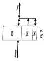
- FIG. 9shows an extension of an on-chip program or configuration memory according to DE 196 54 846.2 by one BIST function shown according to the procedure described.
- the usual memory area (0901)is after State of the art through a non-volatile memory area (0902) is usually implemented as ROM - although one Design as (E) EPROM, FLASH-ROM, NV-RAM etc. possible would be expanded in which the test data, i.e. the test algorithms and test vectors are stored.
- EEPROM
- FLASH-ROMFLASH-ROM
- NV-RAMetc. possible would be expanded in which the test data, i.e. the test algorithms and test vectors are stored.
- At the end of memoryanother memory area (0903) has been added. This is a few entries in size and contains the addresses more defective PAEs and / or broken buses that are in the counters / registers (0108) can be loaded.
- This storage areais considered not volatile read / write memory configured (flash ROM, EEPROM, NV-RAM, etc.). This means that the data can be read out during the RESET and after a test algorithm has expired, where a repairable error has been found using the current data are overwritten. This data is either depending on the implementation of the meters (0108, bus 0114) or from the lookup tables.
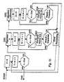
- FIG. 10shows the example of a standard processor with implemented troubleshooting.
- the processoris connected to its periphery via the bus interface (1001).
- Two multiplexers (1002 and 1003)are assigned to the bus interface, 1002 controlling two alternative code caches (1004, 1005) and 1003 two alternative data caches (1006, 1007) in such a way that only one of the caches is used in each case. This means that a cache is available to compensate for defects and can be addressed via the multiplexers.
- the code cacheleads via a multiplexer (1008) to the control unit (1009) of the processor, which in this example only exists once.
- the integer arithmetic units (1010, 1011, 1012) and the floating point arithmetic units (1013, 1014, 1015)are controlled by the control unit. Two arithmetic units are used in operation, a third is available if one of the arithmetic units fails.
- Two integer arithmetic unitsare each connected to the data bus (1018) via the bidirectional multiplexers (1016, 1017), and two floating point arithmetic units are each connected to the data bus (1018) via the bidirectional multiplexers (1019, 1020).
- the data busis connected to the data cache via a bidirectional multiplexer (1021).
- the multiplexer 1003is also designed bidirectionally. The multiplexers are controlled according to the method already described.
- the multiplexers 1002, 1008, the multiplexers 1003, 1021, the multiplexers 1016, 1017 and the multiplexers 1019, 1020each form a dependent group.
- the data and code cache, as well as a floating point and integer arithmetic unitcan be replaced within the example processor according to the described method.
- n, n ⁇ (1, 2, 7)the index of all Algorithms and defines the currently used algorithm.
- Each algorithmis in a first position (1101), which corresponds to FIG. 7a, and a second mirrored one Positioning (1102), which corresponds to FIG. 7b, in front.
- the variable m, m ⁇ (1, 2, ...)is the index of the calculating and comparing test vectors.
- nn + 1). If n reaches the value after the last valid one Algorithm, the test is aborted.
- FIG. 12ashows the generation of new multiplexer states via a counter.
- a non-volatile read-write memoryeg 0903
- vis increased until either the test runs correctly or v reaches the position behind the last PAE and it has been proven that the faulty group of PAEs cannot be corrected, either because of the error elsewhere (e.g. bus system), or two or more PAEs are defective. 12b shows a less time-consuming possibility.
- the lookup tablealready described is integrated. It receives the indices m and n as the input value, as well as the number of the comparator that determined the error. This number is supplied by ErrorCHK (0706) via bus 0707. The lookup table returns the number v of the defective PAE. Then the failed test is run again.
- FIG. 13shows one possibility of a chip test during IDLE cycles, these are cycles during which no program execution takes place because of an action (e.g. a Keyboard input) is to be performed. Usually such cycles are created by holding loops in the program code expressed. It is readily possible if there is one such a waiting condition to call a test routine that performs a test of the chip while waiting, wherein however, a real-time capability in responding to that waiting action is no longer possible.
- the known from Fig. 11 Indices m and nhave the same meaning in FIG. 13 accepted. However, the indexes are in data storage stored. All relevant data in the array are pre the call of the test routine is saved and after execution the test routine restored. When calling the test routine the indices are first loaded from the data store.
- FIG. 14shows a possible modification from FIG. 13, in which the test routine directly from the user program is called (call TEST_CHIP (m, n)).
- the test routinewill called at certain suitable points in the algorithm. All relevant data in the array are saved beforehand and restored after executing the test routine. The indices m, n are also passed on directly when called. Within the routine TEST_CHIP algorithm n is included the data m executed. The error test takes place according to FIG. 11 and Fig. 13 instead. At the end of TEST_CHIP are the indices in contrast to FIGS. 11 and 13, not recalculated. The Return from the routine TEST_CHIP leads to the position directly after the call "call TEST_CHIP", comparable to the BASIC standard GOSUB ... RETURN.
- the lookup table (1501)is implemented as ROM.
- the indices m, n; that is, the identifier of what is currently being performed Test algorithm, the identification of the current test data, and the result (0707) of the ErrorCHK unit (0706)are supplied to the ROM as addresses (1502).
- the resulting Data (1503)give the number of the defective PAE on. This number is transferred to the register (0108).
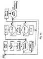
- 16shows a fault-tolerant bus system.
- a set of the same buses (1601)is an additional one Bus (1602) assigned.
- the bus systemhas connections in all four directions.
- About Multiplexers (1603)the connections to the buses are switched so that at a failure of one bus, its function by the neighboring one (Underneath in the horizontal or right lying in the vertical) bus is taken over. In doing so all multiplexers connected to a specific bus are addressed by the same control line, for example multiplexers 1603a are connected to bus 1601a are controlled by the control line 1604a.
- the Control lines 1604are matched by one unit 0109 from FIG. 1. Further control and error handling is basically the same as in the previous ones Figures described.
- FIG. 17shows the assignment of an on-chip RAM or RAM area (1701) to a group of cells (1702).
- the cells (1702)are stored in the RAM or RAM area (1701).
- the datawritten back to the internal registers of the cells.
- the datais written and read via the Multiplexer / gates (0103, 0104 and 0105). This will make the Data from a defective cell according to the position the multiplexer to the cell connected for replacement written.
- the sequence of the user algorithmis determined by does not affect the test procedure.
- Fig. 18shows the system described in Fig. 17, however the data of the cells in the chip (1801) into an external Memory (1802) written, or from external memory read.
- Fig. 19the use of explicit test registers TestReg- n is shown.
- Each internal register Reg- n a cell (1902)is assigned (1903) a method used for the test algorithms TestReg- register n.
- the demultiplexer (the gate) (1901)is used to select which register is written to;
- the multiplexer (1904)is used to select which register is read from.
- the control of the (de) multiplexer (1901, 1904)in such a way that in normal operation, ie, is selected during the course of the user algorithms that Reg- n (1902) and in the execution of the test algorithm the n TestReg- (1903 ) is used. 19 is implemented for each relevant register within a cell.
- the disadvantage of the circuitis that the data of a defective cell is not available to the one connected as a replacement.
- At least a method for repairis thus also described of integrated circuits, being a single or a plurality of modules, another identical additional module is assigned to the inputs of the modules a multiplexer is connected upstream, the one of the input bus Switch the module to the following module can, a multiplexer is connected downstream of the module outputs which is the output bus of a module of the respective subsequent assembly can receive, in the case of a Defects in one of the modules switched the multiplexers in this way be that the defective assembly by its successor is replaced, the subsequent assembly by their Subsequent is replaced until the last assembly is replaced by the additional module.
- the control of the multiplexerdone by a decoder that encodes a binary value so that either all multiplexers are switched the same or two groups of successive multiplexers arise, the multiplexers being the same within a group switched, but the two groups switched differently are, so a defective assembly from the multiplexers is excluded.
- the binary valueis generated by a counter. Then it can also be provided that the counter in the event of an error is incremented or decremented until the defective module has been reached, or an end value has been reached becomes.
- the binary valuecan be through a lookup table to be generated. The lookup table can then be based on the performed test and the detected error the binary value deliver the defective assembly.
- the binary values of the defective Modulescan be stored in a chip-internal memory to immediately when the system is restarted to be available and / or the binary values of the defective Modules can be stored in an external chip memory will be used to restart the system To be available, it is also possible that the binary values the defective assemblies from a higher-level unit are managed and overall it is possible that the modules represent bus systems.
- Circuitswhich is characterized by that the function of the integrated circuit is tested is carried out by executing a test program, whereby test vectors be calculated and there is an error if the comparison of the results with a predetermined target result is false, it is preferably possible that in two or multi-dimensional arrays from multiple arithmetic units of the test algorithm exchanged / mirrored at least once within the array is and is also preferably possible that the test data are stored in an internal memory and / or the test data are in an external block Memory are located, whereby it is possible that the Test data can be loaded from a higher-level unit and / or the control of the self-test takes place within the module and / or the control of the self-test by a parent unit takes place.
- the self-testcan be carried out when the system is started are, and / or during the waiting cycles of the running application program (IDLE cycles) carried out and / or by Application program can be called and / or in an application program be integrated.
- IDLE cyclesrunning application program
Landscapes
- Engineering & Computer Science (AREA)
- General Engineering & Computer Science (AREA)
- Theoretical Computer Science (AREA)
- Physics & Mathematics (AREA)
- General Physics & Mathematics (AREA)
- Computer Hardware Design (AREA)
- Quality & Reliability (AREA)
- Tests Of Electronic Circuits (AREA)
- Design And Manufacture Of Integrated Circuits (AREA)
- Semiconductor Integrated Circuits (AREA)
- Test And Diagnosis Of Digital Computers (AREA)
- Internal Circuitry In Semiconductor Integrated Circuit Devices (AREA)
Abstract
Description
Translated fromGermanAus DE 196 51 075.9-53 sind Prozessoren mit einer Mehrzahlvon 2- oder mehrdimensional angeordneten Rechenwerken/Zellenbekannt. Die Rechenleistung derartige Prozessoren steigt mitder Zahl der vorhandenen Rechenwerken an. Daher wird versuchtmöglichst viele Rechenwerke auf einen Chip zu integrieren,wodurch die benötigte Fläche ansteigt. Mit steigender Fläche,wächst gleichzeitig die Wahrscheinlichkeit, dass der Chip bereitsbei der Herstellung Fehler aufweist und unbrauchbarist. Demselben Problem unterliegen alle in Matrix-Form angeordneteRechenwerke, z.B. auch andere bekannte bekannten Typenwie DPGAs, Kress-Arrays, Systolische Prozessoren und RAW-Machines;genauso wie einige Digitalen Signalprozessoren(DSPs), die mehr als ein Rechenwerk besitzen.
Gleichzeitig sind allen genannten Typen sehr testintensiv,d.h. um die Fehlerhaftigkeit nachzuweisen müssen besondersviele Testfälle in bezug auf die Funktion der Zellen und Vernetzunggeneriert und getestet werden. Herkömmliche bekannteMethoden wie BIST, Boundary Scan, etc. sind aufgrund der erheblichen Menge an Testvektoren schlecht zu integrieren undzu zeit- und platzintensiv.Processors with a plurality of arithmetic units / cells arranged in two or more dimensions are known from DE 196 51 075.9-53. The computing power of such processors increases with the number of existing arithmetic units. Therefore, attempts are made to integrate as many arithmetic units as possible on one chip, which increases the required area. With increasing surface area, the probability increases that the chip already has defects during manufacture and is unusable. All arithmetic units arranged in matrix form are subject to the same problem, for example also other known types such as DPGAs, Kress arrays, systolic processors and RAW machines; just like some digital signal processors (DSPs) that have more than one arithmetic unit.
At the same time, all of the types mentioned are very test-intensive, ie in order to prove the defectiveness, a particularly large number of test cases must be generated and tested with regard to the function of the cells and networking. Conventional known methods such as BIST, Boundary Scan, etc. are difficult to integrate due to the considerable amount of test vectors and are too time and space intensive.
Standardprozessoren wie beispielsweise die bekannte x86-Reihe,MIPS oder ALPHA besitzen mehrere Rechenwerke, diezeitversetzt oder durch einen VLIW-Befehl gleichzeitig angesteuertwerden. In Zukunft wird die Zahl der integrierten Recheneinheiten(Integer-Units) und Fließkomma-Rechenwerke(Floating-Point-Units) weiter ansteigen. Jedes der Rechenwerkemuß ausreichend getestet werden und weitestgehend fehlerfreisein.Standard processors such as the well-known x86 series,MIPS or ALPHA have several arithmetic units thatdelayed or controlled simultaneously by a VLIW commandbecome. In the future the number of integrated computing units(Integer units) and floating point arithmetic units(Floating point units) continue to rise. Each of the arithmetic unitsmust be adequately tested and largely error-freehis.
Durch die steigende Fehlerwahrscheinlichkeit bei großen Chipskönnen entweder nur sehr wenige Zellen integriert werden,oder die Produktionskosten werden bedingt durch den entstehendenAusschuß erheblich. Bei sehr großen Chips wird einemaximale Fläche erreicht, über der hinaus kein funktionsfähigerChip mehr hergestellt werden kann.
Durch den Zeitaufwand beim Testen nach herkömmlichen Verfahrensteigen die Testkosten stark an. Eingebaute BIST-Funktionen(Build In Self Test) verschwenden durch hohen Zusatzaufwandsehr viel Fläche, die die Kosten nach oben treibtund die Herstellbarkeit verringert. Zudem steigt die Wahrscheinlichkeitstark an, dass ein Fehler nicht innerhalb dereigentlichen Funktionseinheiten sonderen innerhalb der Teststrukturenliegt.Due to the increasing probability of errors with large chips, only very few cells can be integrated, or the production costs become considerable due to the resulting scrap. With very large chips, a maximum area is achieved beyond which a functional chip can no longer be produced.
Due to the time required for testing according to conventional methods, the test costs increase significantly. Built-in BIST functions (Build In Self Test) waste a lot of space due to the high additional effort, which drives up costs and reduces producibility. In addition, the likelihood increases that an error is not within the actual functional units but rather within the test structures.
Durch die steigende Zahl der Rechenwerke steigt die Fehlerwahrscheinlichkeitan. Dadurch bedingt wird der Ausschuß höher,wodurch die Herstellungskosten steigen. Mit wachsenderFläche und der damit verbundenen Steigerung der Transistormengewächst die Ausfallwahrscheinlichkeit bei der Benutzung.Bezüglich des Testaufwandes und der BIST-Implementierung giltdas bereits für "Mehrdimensionale Arrays aus Rechenwerken"Gesagte.The probability of errors increases due to the increasing number of arithmetic unitson. This increases the committeewhich increases manufacturing costs. With growingArea and the associated increase in the amount of transistorsthe probability of failure during use increases.Regarding the test effort and the BIST implementation appliesalready for "multidimensional arrays from arithmetic units"Said.
Aus der US-PS 5,072,178 ist ein Verfahren zum Testen einesLogikschaltkreises bekannt, welches Daten verändern kann, wobeieine Testapparatur und eine Vorrichtung beschrieben werden.Die bekannte Logikschaltkreistestvorrichtung weist einenersten Speicher auf, um Testdaten einschließlich einer Vielzahlvon Testmustern zu speichern, und einen zweiten Speicher,um jedes der Testmuster in Übereinstimmung mit einerGruppe von Testeranschlüssen zu speichern und weist weitereinen Transferschaltkreis mit einem Datenkonverter auf, umdie Testmuster aus dem ersten Speicher und einem drittenSpeicher zu ändern, um Kontrolldaten festzulegen, um den Datenkonverterzu kontrollieren.From US-PS 5,072,178 is a method for testing aLogic circuit known, which can change data, wherebya test apparatus and a device are described.The known logic circuit test device has onefirst memory to test data including a varietyof test patterns, and a second memory,around each of the test patterns in accordance with oneStore group of tester connections and points furthera transfer circuit with a data converter tothe test patterns from the first memory and a thirdChange memory to set control data to the data converterto control.
Gemäß der vorliegenden Erfindung ist es möglich defekte Zellendurch Funktionsfähige zu ersetzen und damit den Ausschußzu verringern. Dabei kann eine Ersetzung entweder mittelsTestsystemen bei der Herstellung der Chips erfolgen oder sogarbeim Anwender im komplett aufgebauten System.
Es ist möglich Testvektoren gemäß dem BIST-Prinzip innerhalbdes Chips, als auch gemäß einem neuen Verfahren außerhalb desBausteins zu generieren, um Fläche und Kosten zu sparen.Weiterhin wird eine Möglichkeit beschrieben, wie Chips automatischDefekte reparieren können, ohne dass ein externes zusätzlichesWerkzeug dafür notwendig ist.
Sämtliche Tests und Reparaturen können zur Laufzeit der Chipsdurchgeführt werden.
Diese Aufgabe wird enfindungsgemäß durch die Merkmaleder unabhängige Ansprüche 1 and 2 gelöst.
Der abhängige Anspruch 3 spezifiert einezweckmäßige Ausgestaltung des Gegestandes ihresHanptanspruchs.According to the present invention, it is possible to replace defective cells with functional ones and thus to reduce rejects. It can be replaced either by means of test systems in the manufacture of the chips or even by the user in the completely assembled system.
It is possible to generate test vectors according to the BIST principle inside the chip, as well as according to a new method outside the chip, in order to save space and costs. Furthermore, a possibility is described how chips can automatically repair defects without the need for an additional external tool.
All tests and repairs can be carried out at runtime of the chips.
According to the invention, this object is achieved by the features of
Dependent claim 3 specifies an expedient configuration of the subject matter of your claim.
Einer Gruppe von Zellen, die im Weiteren in Anlehnung an DE196 51 075.9-53 mit PAEs bezeichnet werden, wird eine zusätzliche,im normalen Betrieb nicht benutzte PAE zugeordnet (dieim Folgenden PAER genannt wird). Die Zellen können Rechenwerkejeder Art, konfigurierbare (programmierbare) Logikzellenoder andere Cores beliebiger Funktion sein. Bei der Gruppierungder PAEs und der Zuordnung der PAER ist eine spaltenoderzeilenweise Gruppierung der PAEs vorzuziehen, da hierdurchdie Vernetzung vereinfacht wird. In Hinblick auf zukünftigeChiptechnologien, wird auf eine mögliche Gruppierungder PAEs innerhalb einer 3. Dimension hingewiesen. Vor dieEingänge der PAEs werden derart Multiplexer geschaltet, dassder Eingang ersten PAE in der Zeile/Spalte auch auf den Eingangder zweiten PAE in der Zeile/Spalte geschaltet werdenkann, wobei dann auch der Eingang der zweiten PAE auf denEingang der dritten PAE geschaltet wird und so weiter. DerEingang der letzten PAE wird auf den Eingang der PAER geschaltet.Das bedeutet, dass bei einem Defekt der ersten PAEderen Funktion durch die Zweite, die Funktion der Zweitendurch die Dritte und so weiter ersetzt wird, bis die Funktionder letzten PAE durch die PAER ersetzt wird. Ist eine PAE innerhalbder Spalte/Zeile defekt, werden die vor ihr liegendenPAEs normal beschaltet und ab der Stelle der defekten PAE alleFunktionen um eine PAE verschoben. Ist beispielsweise diePAE 4 defekt, so führen die PAEs 1..3 ihre jeweilige Funktionaus, während der Eingangsmultiplexer der PAE 5 so geschaltetist, dass er die Daten der PAE 4 erhält, der Eingangsmultiplexerder PAE 6 erhält die Daten der PAE 5 und so weiter,bis der Eingang der PAER die Daten der letzten PAE erhält.A group of cells that are based on DE196 51 075.9-53 with PAEs, an additional,PAE not used in normal operation (thehereinafter referred to as PAER). The cells can do arithmeticany type, configurable (programmable) logic cellsor other cores of any function. When groupingthe PAEs and the assignment of the PAER is a column orline-by-line grouping of the PAEs is preferable because of thisnetworking is simplified. With regard to futureChip technologies, is based on a possible groupingof the PAEs within a 3rd dimension. Before thatMultiplexer inputs are switched in such a way thatthe input first PAE in the row / column also on the inputthe second PAE in the row / columncan, and then the input of the second PAE to theInput of the third PAE is switched and so on. TheThe input of the last PAE is switched to the input of the PAER.This means that if there is a defect in the first PAEtheir function by the second, the function of the secondis replaced by the third party and so on until the functionthe last PAE is replaced by the PAER. Is a PAE insideof the column / row is defective, the ones in front of it arePAEs wired normally and all from the point of the defective PAEFunctions shifted by one PAE. For example, is thatPAE 4 defective, the
Um die Ergebnisse wieder in der richtigen Reihenfolge derVernetzung zuzuführen werden an den Ausgängen der PAEs ebenfallsMultiplexer angebracht, wobei der Ausgangsmultiplexerder PAE 1 entweder die PAE 1 auf den Bus schaltet - soferndiese nicht defekt ist - oder bei einem Defekt den Ausgangder PAE 2 auf den Bus schaltet, an Stelle der PAE 2 wird danndie PAE 3 auf den Bus geschaltet, bis hin zur letzten PAE, anderen Stelle die PAER aufgeschaltet wird. Befindet sich diedefekte PAE in der Mitte der Zelle/Spalte, so erfolgt eineVerschiebung der Ausgänge in genau der Art, wie sie für dieEingänge bereits beschrieben wurde.
Speziell bei konfigurierbarer Logik und konfigurierbaren Rechenwerken,treten zusätzliche Bussysteme auf, um die Konfigurationsdatenzu übermitteln und die Konfiguration zu steuern.Diese Bussysteme werden entsprechend der in diesem Abschnittgenannten Busse ebenfalls über Multiplexer verschaltet.Gleiches gilt für die Bussysteme, über die bei einer matrixartigenAnordnung von Rechenwerken (z.B. Systolische Prozessoren,SIMD, etc), die Befehle in die jeweiligen Rechenwerkegeschrieben werden.
Grundsätzlich kann jeder Bus oder jedes Signal über Multiplexergeleitet werden. Je nach Anforderung an die Ausfallsicherheitkann beispielsweise das Taktsignal über Multiplexergeführt werden, um einem eventuellen Kurzschluß vorzubeugen;oder das Taktsignal wird direkt an die Zelle geführt, weilein derartiger Ausfall nicht abgefangen werden soll. Die Stufeder Ausfallsicherheit kann konstruktiv entsprechend denAnforderungen für jedes Signal oder jeden Bus einzeln festgelegtwerden.To feed the results back in the correct order of networking, multiplexers are also attached to the outputs of the PAEs, whereby the output multiplexer of the
Especially with configurable logic and configurable arithmetic units, additional bus systems occur in order to transmit the configuration data and to control the configuration. These bus systems are also connected via multiplexers in accordance with the buses mentioned in this section. The same applies to the bus systems via which the commands are written into the respective arithmetic units in the case of a matrix-like arrangement of arithmetic units (for example systolic processors, SIMD, etc.).
In principle, every bus or signal can be routed via multiplexers. Depending on the requirements for reliability, for example, the clock signal can be routed via multiplexers to prevent a possible short circuit; or the clock signal is fed directly to the cell because such a failure should not be intercepted. The level of failure safety can be determined individually for each signal or bus according to the design requirements.
Das vorgestellte Konzept zur Fehlerkorrektur innerhalb vonGatterstrukturen ist in gleicher Weise auf Bussysteme anwendbar.Dabei wird einer Anzahl von Bussen (Bus 1 ... Bus n) einzusätzlicher Bus (BUS R) zugeordnet. Ist einer der Busse defekt(BUS d), wird seine Funktion von einem seiner Nachbarbusseübernommen (BUS (d + 1)). Die Funktion des Nachbarbusses(BUS (d + 1)) wird von dessen Nachbarbus (BUS (d + 2))übernommen, usw., wobei die Richtung des übernehmenden Busseimmer die gleiche bleibt. So lange, bis BUS n durch BUS Rübernommen wird.
Bei der Anwendung der Multiplexer-Strukturen auf Bussystemewerden entsprechend der vorliegenden Verbindungsstruktur undder Richtung der Daten gewöhnliche Multiplexer, Dekoder undGates, Tristate-Gatter, oder Bidirektionale Multiplexer eingesetzt.The concept presented here for error correction within gate structures can be applied in the same way to bus systems. An additional bus (BUS R) is assigned to a number of buses (
When the multiplexer structures are used on bus systems, conventional multiplexers, decoders and gates, tristate gates or bidirectional multiplexers are used in accordance with the connection structure and the direction of the data.
Es ist offensichtlich, dass immer zwei Gruppen von aufeinanderfolgendenMultiplexern denselben Zustand annehmen müssen,d.h. MUX 1 = MUX 2 = MUX3 = ... = MUX n = Zustand A und MUX(n + 1) = MUX (n + 2) = MUX (n + 3) = ... = MUX m = ZustandB.
Ist keine PAE defekt gilt MUX 1 = MUX 2 = ... = MUX m = ZustandA.
Ist die erste PAE defekt gilt MUX 1 = MUX 2 = ... = MUX m =Zustand B.
Ist beispielsweise PAE 3 defekt gilt MUX 1 = MUX 2 = ZustandA, MUX 3 = MUX 4 = ... = MUX m = Zustand B, wobei in diesemBeispiel PAER der PAE m zugerordnet ist, d.h. PAER befindetsich direkt neben PAE m.It is obvious that always two groups of successive multiplexers have to assume the same state, ie
If no PAE is defective,
If the first PAE is defective,
If, for example, PAE 3 is defective,
Die Ansteuerung der Multiplexer sieht daher beispielsweisewie folgt aus
Ist die PAER der PAE 1 zugeordnet, so ist die Reihenfolgem...1 vertauscht (Defekte PAE 1 entspricht 0000...001, bzw.defekte PAE m entspricht 1111...111).If the PAER is assigned to
Es ist daher ausreichend die Nummer der defekten PAE zu speichernund diese einem Dekoder zuzuführen, der anhand der obenabgebildeten Tabelle die Zustände der Multiplexer ansteuert.It is therefore sufficient to save the number of the defective PAEand feed them to a decoder, which is based on the aboveshown table controls the states of the multiplexers.
Grundsätzlich können beliebige Teststrategien auf das Verfahrenangewendet werden, wobei das folgende erfindungsgemäßeVerfahren als besonders geeignet angesehen wird:
Das Array aus PAEs wird mit einem oder mehreren Testalgorithmengeladen, die ein oder mehrere Testvektoren berechnen. Aneiner Kante des Arrays werden die PAEs als Vergleicher geschaltet,so dass die anhand der Testvektoren berechnetenWerte mit den Sollergebnissen verglichen werden. Entsprichtdas berechnete Ergebnis nicht den Sollergebnissen liegt ein Fehler vor. Die Testdaten, also die Testalgorithmen, dieTestvektoren und die Sollergebnisse liegen dabei in einem internenoder externen Speicher vor oder werden von einer übergeordnetenEinheit geladen. Es ist bei dieser Teststrategienotwendig, dass ein jeder Testalgorithmus mindestens zweimalberechnet wird, wobei beim zweiten Mal die als Vergleicherausgestalteten PAEs an einer anderen Kante liegen (vorzugsweiseder gegenüberliegenden), um eine Ausführung des Testalgorithmussesauf allen PAEs zu gewährleisten. Ebenfalls istes denkbar, dass die Vergleicher im Inneren des PAE-Arraysangeordnet sind und von links und rechts (oben und unten) jeweilsein Testalgorithmus A und B je ein Ergebnis A und B berechnet,wobei die Ergebnisse den Vergleichen zugeführt werdenund übereinstimmen müssen.
Abhängig von der Art des Testalgorithmusses kann die fehlerhaftPAE anhand des Fehlers zurückverfolgt werden oder nicht.Unterstützt der Algorithmus eine Zurückverfolgung , so werdendie entsprechenden Multiplexer-Zustände der Zeile/Spalte inder sich die defekte PAE befindet geändert und den Multiplexernzugeführt. Der Testalgorithmus, bei dem der Test fehlschlugwird erneut ausgeführt um eine Fehlerfreiheit, die nungegeben sein sollte zu überprüfen. Ist der Baustein weiterhinfehlerhaft, muß überprüft werden, ob eventuell weitere oderandere PAEs defekt sind. Dabei ist die Ausführung des Testalgorithmussesund die Generierung der dem Fehler angepaßtenMültiplexerzustände iterativ.
Üblicherweise ist es nicht ausreichend nur einen Testalgorithmuszu implementieren, vielmehr müssen mehrere unterschiedlicheTestalgorithmen implementiert sein, die jeweilsmit mehreren Testvektoren geprüft werden. Nur so ist eine maximaleFehlererkennungsrate zu erreichen. Gleichzeitig mußdie Busvernetzung von Testalgorithmus zu Testalgorithmus geändert werden, damit auch die Bussysteme ausreichend geprüftwerden.
Auf die verschiedenen Ausführungen der Testalgorithmen wirdin nicht nähers eingegangen, da dies für das erfindungsgemäßeGrundverfahren nicht relevant ist.In principle, any test strategies can be applied to the method, the following method according to the invention being regarded as particularly suitable:
The array of PAEs is loaded with one or more test algorithms that calculate one or more test vectors. At one edge of the array, the PAEs are switched as comparators, so that the values calculated on the basis of the test vectors are compared with the target results. If the calculated result does not correspond to the target results, there is an error. The test data, that is to say the test algorithms, the test vectors and the target results are available in an internal or external memory or are loaded by a higher-level unit. With this test strategy it is necessary that each test algorithm is calculated at least twice, the second time the PAEs designed as comparators are located on a different edge (preferably the opposite one) in order to ensure that the test algorithm is executed on all PAEs. It is also conceivable for the comparators to be arranged in the interior of the PAE array and for each test algorithm A and B to calculate a result A and B from the left and right (top and bottom), the results being fed to the comparisons and having to agree ,
Depending on the type of test algorithm, the faulty PAE may or may not be traced back based on the fault. If the algorithm supports traceability, the corresponding multiplexer states of the row / column in which the defective PAE is located are changed and fed to the multiplexers. The test algorithm in which the test failed is executed again in order to check that there is no error, which should now be given. If the block is still faulty, it must be checked whether further or other PAEs are defective. The execution of the test algorithm and the generation of the multiplexer states adapted to the error are iterative.
It is usually not sufficient to implement just one test algorithm; rather, several different test algorithms must be implemented, each of which is checked with several test vectors. This is the only way to achieve a maximum error detection rate. At the same time, the bus network must be changed from test algorithm to test algorithm so that the bus systems are also adequately checked.
The various versions of the test algorithms are not dealt with in more detail, since this is not relevant to the basic method according to the invention.
Bausteinen wie DE 196 51 075.9-53, DPGAs, Kress-Arrays, SystolischeProzessoren und RAW-Machines gemeinsam ist ein integrierterSpeicher, der einem oder mehreren PAEs zugeordnetist und die Funktion des/der Rechenwerke bestimmt.
Entsprechend des BIST Grundprinzips wird der Speicher um einenBereich (TestMEM) erweitert, der die Testalgorithmen und-vektoren enthält. Dabei kann dieser Speicher fest in Formeines ROMs oder wiederbeschreibbar mittels (E)EPROM, Flash-ROM,NV-RAM oder ähnlichem ausgestaltet sein.
Um einen Selbsttest durchzuführen wird an eine Speicherstelleinnerhalb des TestMEM gesprungen und die dort abgelegteTestroutine ausgeführt (Internal Driven Self Test = IDST).Dabei sind außer der Erweiterung des Speichers (um den TestMEM)und einer Auswerteeinheit für die bereits beschriebenenVergleicher (ErrorCHK) keine weiteren BIST-typischen Zusatzbaugruppenauf dem Chip notwendig.Modules such as DE 196 51 075.9-53, DPGAs, Kress arrays, systolic processors and RAW machines together are integrated memories that are assigned to one or more PAEs and determine the function of the processor (s).
In accordance with the BIST basic principle, the memory is expanded by an area (TestMEM) that contains the test algorithms and vectors. This memory can be configured in the form of a ROM or can be rewritten using (E) EPROM, Flash-ROM, NV-RAM or the like.
To carry out a self-test, you jump to a memory location within the TestMEM and the test routine stored there is executed (Internal Driven Self Test = IDST). Apart from the expansion of the memory (by the TestMEM) and an evaluation unit for the comparators (ErrorCHK) already described, no further BIST-typical additional modules on the chip are necessary.
Durch die Verringerung der Baugruppen auf eine Speichererweiterung(TestMEM) und einer Auswerteeinheit der Vergleicher(ErrorCHK) wird eine weitere noch kostengünstigere und platzsparendereVariante ermöglicht. Dabei wird kein internerTestMEM implementiert, vielmehr wird der gewöhnliche interneSpeicher von außen mit dem Testalgorithmus und den Testvektorengeladen (External Driven Self Test = EDST); das bedeutet, die BIST-Testdaten werden nach außen verlagert und wie einnormales Programm betrachtet. Danach wird der Testalgorithmusausgeführt. Alternativ kann der Testalgorithmus auch währendder Ausführung sucessive aus einem externen Speicher geladenund dekodiert werden. Lediglich die ErrorCHK-Einheit muß nochauf dem Chip integriert sein. Um den Testalgorithmus und dieTestvektoren von außen in den/die chipinternen Speicher zuladen gibt es mehrere Möglichkeiten. Prinzipiell kann derVorgang durch eine funktionell übergeordnete CPU oder Recheneinheit(HOST) erfolgen, in dem diese die Testdaten (Testalgorithmusund Testvektoren) auf den Chip lädt (Download) oderder Chip lädt die Testdaten selbständig aus einem externen(Dualported-)RAM oder Festspeicher wie ROM, (E)EPROM, Flash-ROM,NV-RAM, o.ä..By reducing the modules to a memory expansion(TestMEM) and an evaluation unit of the comparators(ErrorCHK) will be another more cost-effective and space-savingVariant allows. No internalTestMEM implemented, rather the ordinary internalExternal memory with the test algorithm and the test vectorsloaded (External Driven Self Test = EDST); that means,the BIST test data is shifted to the outside and like aconsidered normal program. After that the test algorithmexecuted. Alternatively, the test algorithm can also be used duringthe execution sucessive loaded from an external memoryand be decoded. Only the ErrorCHK unit still has tobe integrated on the chip. To the test algorithm and theTest vectors from the outside into the on-chip memorythere are several ways to load. In principle, theProcess by a functionally higher-level CPU or computing unit(HOST) in which the test data (test algorithmand test vectors) onto the chip (download) orthe chip automatically loads the test data from an external one(Dual-ported) RAM or permanent memory such as ROM, (E) EPROM, Flash-ROM,NV-RAM, etc.
BIST-Verfahren nach den Stand der Technik führen den Selbsttestfür gewöhnlich nur während der RESET-Phase, also kurznach dem Anlegen der Spannung (dem Einschalten), des Chipsdurch. Im Gegensatz dazu ist es möglich bzw. sinnvoll die indieser Schrift beschriebenen Verfahren während der Laufzeitder Programme auf den Chips durchzuführen. Beispielsweisekann ein kompletter Test des Chips während der RESET-Phasedurchgeführt werden und jeweils ein Teil der vorhandenenTestdaten während der Ausführung des Anwenderprogrammes bzw.während sogenannter IDLE-Zyklen, das sind Zeiträume, in denenkein Programm auf den Chips läuft, bzw. der Chip im Wartezustandist. Dies ist ohne weiteres möglich, in dem während denIDLE-Zyklen einer der Testalgorithmen im internen Speicherangesprungen wird, bzw. vom externen Speicher oder HOST inden Baustein geladen wird. Dabei ist es verständlicherweisemöglich, aus der Mehrzahl der vorhandenen Testalgorithmen und Testdaten partiell einen oder mehrere auszuwählen, wobei dieAnzahl der ausgewählten Testdaten anhand der Länge des IDLE-Zyklussesfestgelegt werden kann. Es können so lange neueTestdaten geladen werden, bis der IDLE-Zyklus durch das Eintreffenneuer zu verarbeitender Daten oder eines neu abzuarbeitendenProgrammes oder einer anderen Anforderung beendetwird.
Eine weitere Möglichkeit ist das feste Integrieren von Teststrategienin die Anwenderprogramme, um während der Verarbeitungdes Anwenderprogrammes Tests durchzuführen.
In beiden Fällen werden die relevanten Daten, die sich imArray befinden, vor dem Aufruf der Testalgorithmen gesichert.Es bietet sich an, dass die Daten entweder in interne Speicherbereiche(vgl. PACT04) oder die extern angeschlossenenSpeicher gesichert werden. Nach Ausführung der Testalgorithmenwerden die Daten vor der normalen Programmverarbeitungzurückgelesen.BIST methods according to the prior art usually only carry out the self-test during the RESET phase, that is to say shortly after the voltage (switching on) has been applied to the chip. In contrast, it is possible or sensible to carry out the methods described in this document on the chips during the runtime of the programs. For example, a complete test of the chip can be carried out during the RESET phase and some of the test data available during the execution of the user program or during so-called IDLE cycles, i.e. periods in which no program is running on the chips, respectively Chip is waiting. This is easily possible by jumping to one of the test algorithms in the internal memory during the IDLE cycles or by loading them into the block from the external memory or HOST. It is understandably possible to select one or more of the majority of the available test algorithms and test data, whereby the number of selected test data can be determined based on the length of the IDLE cycle. New test data can be loaded until the IDLE cycle is ended by the arrival of new data to be processed or a new program to be processed or another request.
Another possibility is the permanent integration of test strategies in the user programs in order to carry out tests while the user program is being processed.
In both cases, the relevant data in the array are saved before the test algorithms are called. It is advisable that the data be saved either in internal memory areas (see PACT04) or in the externally connected memory. After executing the test algorithms, the data are read back before normal program processing.
Eine Alternative zur Steigerung der Ausführungsgeschwindigkeitbesteht darin, neben jedem Register (Reg-n,n ∈ N) einzusätzliches, nur für die Testalgorithmen verwendetes, Register(TestReg-n,n ∈ N) zu implementieren. Vor Ausführungder Testalgorithmen, werden über Multiplexer/ Demultiplexer(Tore) die TestReg-n zugeschaltet und für den Test verwendet.Die Reg-n bleiben unverändert. Nach Ausführung der Testalgorithmenwerden wieder die Reg-n zugeschaltet.An alternative to increasing the speed of execution is next to each register(s Reg-,n ∈ N) an additional, used only for test algorithms register(s TestReg-, ∈ Ns) to implement. Before performing the test algorithms that TestReg- be switched overn multiplexer / demultiplexer (goals) and used for the test. The Reg-n remain unchanged. After execution of the test algorithms, the Reg- be switchedn again.
Sieht die Teststrategie vor, dass nur Zellen getestet werden,deren Daten im Folgenden nicht mehr relevant sind, kann aufdas Sichern und Laden der Daten auch verzichtet werden.Does the test strategy provide that only cells are testedwhose data are no longer relevant belowbacking up and loading of the data can also be dispensed with.
Wird eine PAE (oder ein Bus) als defekt erkannt, muß deren(dessen) Nummer, also der Zustandvektor (Defektkennung) derzugeordneten Multiplexer gespeichert werden, zum einen um dieMultiplexer anzusteuern, zum anderen um bei einem Neustart(RESET) des Chips sofort zur Verfügung zu stehen.
Hierzu kann die Defektkennung
Defect detection can do this
Üblicherweise wird nach der Erkennung eines Defektes die defekteZelle anhand des erkannten Fehlverhaltens zurückverfolgt.Das ist bei entsprechenden Testalgorithmen möglich,sofern ein zusätzlicher Algorithmus zur Zurückverfolgung desFehlers existiert. Bei Kontrolle des Tests durch einen HOSTkann die Zurückverfolgung auf dem HOST durchgeführt werden.Existiert jedoch kein HOST kann oftmals die Zurückverfolgungnicht innerhalb des defekten Chips integriert werden oder istzu aufwendig.
Zur Lösung wird vorgeschlagen einen ladbaren Zähler vor jedemDekoder zu integrieren. Im Normalfall wird in den Zähler dieNummer der defekten PAE geladen, wonach der Dekoder die Zuständeder Multiplexer wie bereits beschrieben ansteuert. Istunbekannt, welche PAE defekt ist, kann der Zähler bei PAE 0oder PAE m beginnend jede mögliche potentiell fehlerhafte PAEansprechen, indem nach jedem erfolglosen Test der Zählerzustand so lange (je nach Implementierung) um eine PAE verringert(von PAE m aus zählend) oder erhöht (von PAE 0 aus zählend)wird, bis die defekte PAE erreicht wird und der Testordentlich abläuft. Der nun erreichte Zählerzustand wird alsZustandsvektor für die Ansteuerung der Multiplexer gespei-.chert und representiert die defekte PAE. Wird kein funktionsfähigerZählerzustand festgestellt, liegt entweder ein andererFehler vor (evtl. in einer anderern Reihe/Spalte oder einBusfehler) oder es ist mehr als eine PAE defekt.
Ein Nachteil beim Einsatz von Zählern ist, dass sämtlicheMöglichkeiten permutiert werden müssen, bis die fehlerhaftePAE gefunden wurde.
Eine weitere Möglichkeit, die allerding mehr Implemetierungsaufwanderfordert, ist daher der Einsatz von LookUp-Tabellen,die anhand des gerade ausgeführten Testalgorithmusses und desentstandenen Fehlerzustandes in ErrorCHK die entsprechendedefekte PAE auswählen. Dazu ist es jedoch notwendig, dass dieTestalgorithmen und Lookup-Tabellen aufeinander abgestimmtsind. Auf die Abstimmung soll jedoch nicht weiter eingegangenwerden, da diese sehr chipspezifisch und unabhängig vomGrundprinzip ist.After the detection of a defect, the defective cell is usually traced back on the basis of the detected misconduct. This is possible with appropriate test algorithms, provided that an additional algorithm for tracing the error exists. If the test is checked by a HOST, tracing can be carried out on the HOST. However, if there is no HOST, tracing often cannot be integrated within the defective chip or is too complex.
As a solution, it is proposed to integrate a loadable counter in front of each decoder. Normally, the number of the defective PAE is loaded into the counter, after which the decoder controls the states of the multiplexers as already described. If it is unknown which PAE is defective, the counter can address any possible potentially faulty PAE starting with
A disadvantage of using counters is that all possibilities have to be permuted until the faulty PAE has been found.
Another option, which however requires more implementation effort, is therefore the use of LookUp tables, which select the corresponding defective PAE based on the test algorithm just executed and the error state that has arisen in ErrorCHK. However, this requires that the test algorithms and lookup tables are coordinated with one another. However, the vote should not be discussed further, since it is very chip-specific and independent of the basic principle.
Aktuelle und zukünftige Prozessoren enthalten eine Mehrzahlan Integer- und Fließkommaeinheiten. Daher ist das beschriebeneVerfahren direkt auf diese Bausteine anwendbar, in demjeweils eine zusätzliche Einheit implementiert wird und füreventuelle Defekte zur Verfügung steht. Der Test der Prozessorenkann beim Hersteller, während des Startvorganges derComputer oder ebenfalls während der Laufzeit stattfinden. Besonderssinnvoll ist dabei ein Test während des Boot-Vorganges, also dem Starten des Rechners nach einem Reset,der bei PCs vom sogenannten BIOS (Basic Input Output System),durchgeführt wird. Dabei können die entsprechenden Zustandvektorender Multiplexer entweder auf dem Prozessor oder inexternen Speichern, beispielsweise der PC-internen batteriegepuffertenEchtzeituhr (RTC) abgelegt werden.Current and future processors contain a majorityon integer and floating point units. So that's what is describedProcedure directly applicable to these building blocks in whichan additional unit is implemented and forpossible defects is available. Processors testcan at the manufacturer, during the starting processComputer or take place during runtime. Especiallyit makes sense to do a test during the boot process,ie starting the computer after a reset,that of PCs from the so-called BIOS (Basic Input Output System),is carried out. The corresponding state vectors canthe multiplexer either on the processor or inexternal memories, for example the internal battery-backed PCReal-time clock (RTC) can be stored.
Das vorliegende Verfahren ermöglicht den Austausch defekterEinheiten, die in dieser Schrift als Rechenwerke ausgestaltetsind, jedoch generell jede beliebige Einheit eines Chips darstellenkönnen, durch funktionstüchtige. Gleichzeitig wirdein Verfahren aufgezeigt, mit dessen Hilfe Selbsttests einfacher,kostengünstiger und vor oder während des Ablaufs desAnwenderprogrammes durchgeführt werden können. Dadurch wirddie Ausfallsicherheit auch im Betrieb erheblich vergrößert,was insbesondere für ausfallkritische Anwendungen wie Kraftwerksbetriebe,Luft- und Raumfahrt oder Militär von besondererBedeutung ist.The present method enables the replacement of defective onesUnits designed in this document as arithmetic unitsare, but generally represent any unit of a chipcan, by working. At the same timedemonstrated a procedure that makes self-testing easier,cheaper and before or during the expiry of theUser program can be carried out. This willreliability significantly increases in operation,which is particularly important for failure-critical applications such as power plant operations,Aerospace or military specialMeaning is.
Die folgende Diagramme zeigen zur Verdeutlichung Ausführungsbeispieledes erfindungsgemäßen Verfahrens:
- Fig. 1
- Grundschaltung
- Fig. 2
- keine PAE defekt
- Fig. 3
- PAE1 defekt
- Fig. 4
- PAEm defekt
- Fig. 5
- PAE3 defekt
- Fig. 6
- Array aus PAEs mit PAERs
- Fig. 7
- Fehlertolerantes Bussystem
- Fig. 7a
- Prinzip eines Selbsttests erster Teil
- Fig. 7b
- Prinzip eines Selbsttests zweiter Teil
- Fig. 8a
- EDST in einem externen ROM integriert
- Fig. 8b
- EDST in einen externen RAM-Bereich integriert
- Fig. 8c
- EDST direkt vom HOST gesteuert
- Fig. 9
- Beispiel eines chipinternen Speichers mit BIST-Funktionintegriert in eine interne Steuereinheitnach DE 196 54 846.2
- Fig. 10
- Beispiel eines fehlertoleranten Standard-Prozessors
- Fig. 11
- Ablaufdiagramm eines Selbsttests
- Fig. 12
- Ablaufdiagramm der Generierung neuer MultiplexerZustandsvektoren
- Fig. 13
- Ablaufdiagramm eines Selbsttest während des IDLE-Zyklusses
- Fig. 14
- Ablaufdiagramm eines in das Anwendungsprogramm integriertenSelbsttests
- Fig. 15
- Lookup Table zur Fehlerkorrektur
- Fig. 16
- Beispiel eines fehlertoleranten Bussystems
- Fig. 17
- Sichern von Registern Reg-n in chipinterne Speichervor dem Ausführen der Testalgorithmen
- Fig. 18
- Sichern von Registern Reg-n in externe Speicher vordem Ausführen der Testalgorithmen
- Fig. 19
- Abschalten der Reg-n und Zuschalten der TestReg-nvor dem Ausführen der Testalgorithmen
- Fig. 1
- basic circuit
- Fig. 2
- no PAE defective
- Fig. 3
- PAE1 defective
- Fig. 4
- PAEm defective
- Fig. 5
- PAE3 defective
- Fig. 6
- Array of PAEs with PAERs
- Fig. 7
- Fault-tolerant bus system
- Fig. 7a
- Principle of a self-test, first part
- Fig. 7b
- Principle of a self-test, part two
- Fig. 8a
- EDST integrated in an external ROM
- Fig. 8b
- EDST integrated in an external RAM area
- Fig. 8c
- EDST controlled directly by the HOST
- Fig. 9
- Example of an on-chip memory with BIST function integrated in an internal control unit according to DE 196 54 846.2
- Fig. 10
- Example of a fault-tolerant standard processor
- Fig. 11
- Flow chart of a self-test
- Fig. 12
- Flow diagram of the generation of new multiplexer state vectors
- Fig. 13
- Flow chart of a self test during the IDLE cycle
- Fig. 14
- Flow chart of a self-test integrated in the application program
- Fig. 15
- Lookup table for error correction
- Fig. 16
- Example of a fault-tolerant bus system
- Fig. 17
- Back up registers Reg-n in on-chip memory before running the test algorithms
- Fig. 18
- Back up registers Reg-n to external memory before running the test algorithms
- Fig. 19
- Switch off the Reg-n and switch on the TestReg-n before executing the test algorithms
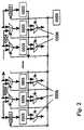
Fig. 1 zeigt das Grundprinzip der fehlertoleranten Verschaltung.Alle PAEs (0101) sind in einer Reihe angeordnet, derletzten PAE ist die zusätzliche PAER (0102) zugeordnet. Vorder ersten PAE in der Reihe ist ein Tor (0103) geschaltet,das die Daten zu der PAE sperrt, sofern diese PAE defekt ist.Ebenfalls ist vor die PAER (0102) ein Tor (0105) geschaltet,das die Daten zur PAER sperrt, wenn diese nicht benötigt wird(oder defekt ist). Die beiden Tore (0103 und 0105) sind optional und nicht zwingend erforderlich. Die Eingangsbusse(0111), die aus einer Mehrzahl von Einzelssignalen zusammengesetztsind, werden über Multiplexer (0104) und die Tore(0103 und 0105) an die PAEs geleitet. Dabei könnnen die Datenab einem Defekt um jeweils eine PAE nach rechts verschobenwerden, bis zur PAER. Den Ausgangsbussen (0112), die aus einerMehrzahl von Einzelssignalen zusammengesetzt sind, vorgeschaltetbefinden sich ebenfalls Multiplexer (0106) die dieErgebnisse im Falle eines Fehlers wieder um eine Positionnach links schieben, so dass der Fehler für das Ergebnisbussystem(Menge aller 0112) nicht erkennbar ist. Die einzelnenAnsteuersignale (0117) für die jeweiligen Multiplexer und Toresind zu einem Bus (0110) zusammengefaßt und werden von einemDekoder (0107) generiert. Der Dekoder erhält die Nummerder defekten PAE von der Einheit 0108, die entweder als Registeroder als ladbarer Zähler ausgestaltet ist. Beim Einsatzeiner Lookup-Tabelle zum Feststellten der defekten PAE ausdem von ErrorCHK generierten Fehler ist 0108 als Register implementiert,in das die Nummer der defekten PAE geladen wird.Wird die fehlerhafte PAE über eine Permutation gesucht,stellt 0108 einen ladbaren Zähler dar, der ausgehend von 0alle möglichen PAEs durchzählt, bis die Fehlerhafte gefundenwurde. Ist die Fehlerhafte bekannt, wird sie beim nächstenRESET-Vorgang direkt in den ladbaren Zähler geladen. Zum Ladendes Zählers oder Registers (0108) steht das Lade-SignalLOAD (0115) zur Verfügung. Um den Zähler hochzuzählen wirddas Signal COUNT (0116) zum Zähler geführt. Über die Signale0114 wird das Ergebnis des Zählers zur Speicherung zurückgeführt.Die Ansteuerung des Zählers/Registers und die Steuerungdes zeitlichen Ablaufs wird von einer nicht gezeichnetenStatemachine, einem externen HOST oder einer Vorrichtung gemäßDE 196 54 846.2 übernommen.Fig. 1 shows the basic principle of fault-tolerant interconnection.All PAEs (0101) are arranged in a row, thethe last PAE is assigned the additional PAER (0102). In fronta gate (0103) is connected to the first PAE in the row,that blocks the data to the PAE if this PAE is defective.A gate (0105) is also connected in front of the PAER (0102),that locks the data to the PAER when it is not needed(or is defective). The two gates (0103 and 0105) are optionaland not absolutely necessary. The input buses(0111), which is composed of a plurality of individual signalsare multiplexers (0104) and the gates(0103 and 0105) to the PAEs. You can use the datafrom a defect shifted one PAE to the rightuntil the PAER. The output buses (0112), which consist of aA plurality of individual signals are composed, upstreamthere are also multiplexers (0106) thatResults in case of an error by one positionslide to the left so that the error for the result bus system(Quantity of all 0112) is not recognizable. The single onesControl signals (0117) for the respective multiplexers and gatesare combined to form a bus (0110) and are managed by oneDecoder (0107) generated. The decoder receives the numberthe defective PAE from
In Fig. 2 sind die Zustände der Multiplexer (0104 und 0106),sowie der Tore (0103 und 0105) angezeigt, wobei keine PAE defektist und die PAER (0102) nicht verwendet wird.2 shows the states of the multiplexers (0104 and 0106),and the gates (0103 and 0105) are displayed, whereby no PAE is defectiveand the PAER (0102) is not used.
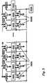
In Fig. 3 sind die Zustände der Multiplexer (0104 und 0106),sowie der Tore (0103 und 0105) angezeigt, wobei die PAE 1(0301) defekt ist und die PAER (0102) verwendet wird.3 shows the states of the multiplexers (0104 and 0106),and the gates (0103 and 0105) are displayed, with PAE 1(0301) is defective and the PAER (0102) is used.
In Fig. 4 sind die Zustände der Multiplexer (0104 und 0106),sowie der Tore (0103 und 0105) angezeigt, wobei die PAE m(0401) defekt ist und die PAER (0102) verwendet wird.4 shows the states of the multiplexers (0104 and 0106),and the gates (0103 and 0105) are displayed, the PAE m(0401) is defective and the PAER (0102) is used.
In Fig. 5 sind die Zustände der Multiplexer (0104 und 0106),sowie der Tore (0103 und 0105) angezeigt, wobei die PAE 3(0501) defekt ist und die PAER (0102) verwendet wird.5 shows the states of the multiplexers (0104 and 0106),and the gates (0103 and 0105) are displayed, with the PAE 3(0501) is defective and the PAER (0102) is used.
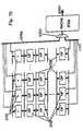
Fig. 6 zeigt ein Array aus PAEs (0601), wobei je einer PAE-Zeileeine PAER (0602) zugeordnet ist und jede Zeile eine separateAnsteuerung (0109, vgl. Fig. 1) besitzt. Dabei könneneine Mehrzahl von Ansteuerungen auch zu einer einzigen denZeilen übergeordneten Ansteuerung zusammengefaßt sein.6 shows an array of PAEs (0601), one PAE line eacha PAER (0602) is assigned and each line is a separate oneControl (0109, see Fig. 1) has. You cana plurality of controls to a single denLines of higher-level control.
Fig. 7a zeigt einen möglichen ersten Test eines Algorithmusses.Dabei sind eine Mehrzahl von PAEs als Rechenelemente(0701) konfiguriert, die jeweils ihre Operation über einenTestvektor durchführen. Dabei sind die PAEs über Bussysteme(0708) beliebiger Ausgestaltung miteinander verbunden. EineReihe der PAEs (0702) ist als Vergleicher konfiguriert. Diein den Rechenelementen berechneten Werte werden in den Vergleichernmit einem vorgegebenen Wert verglichen. Stimmenbeide Werte nicht überein, liegt ein Fehler vor. Die Ergebnisse der Vergleiche werden über ein Bussystem (0705) an einenMultiplexer (0703) geführt, der so geschaltet ist, dasser die Ergebnisse der Vergleiche aus (0702) an eine beliebigausgestaltete Einheit (ErrorCHK 0706) zum Feststellen einesFehlers und eventuell dessen Auswertung weitergereicht wird.Die Fehlerauswertung (0706) gibt ihr Ergebnis über den Bus(0707) an den HOST oder die steuernde Statemachine weiter(vgl. Fig. 1).7a shows a possible first test of an algorithm.There are a number of PAEs as computing elements(0701), each configured its operation via aExecute test vector. The PAEs are via bus systems(0708) connected in any configuration. ARow of PAEs (0702) is configured as a comparator. TheValues calculated in the computing elements are used in the comparatorscompared with a predetermined value. voicesthere is an error if the two values do not match. The resultsthe comparisons are sent to one via a bus system (0705)Multiplexer (0703) performed, which is switched so thatthe results of the comparisons from (0702) to anydesigned unit (ErrorCHK 0706) for determining aError and possibly its evaluation is passed on.The error evaluation (0706) gives its result via the bus(0707) to the HOST or the controlling state machine(see Fig. 1).
Fig. 7b zeigt einen zweiten Test der über die selbe Matrixaus PAEs durchgeführt wird wie Fig. 7b. Der auszuführende Algorithmusist derselbe, ebenso wie die zu berechnenden Werte.Dabei sind jedoch die PAEs der Zeile 0702 als normale Rechenelementeausgestaltet, wobei jedoch die erste Zeile dervorher (Fig. 7a) als Rechenwerke geschalteten PAEs (0701) nunals Vergleicher (0711) ausgestaltet sind. Die Datenflußrichtungauf den Bussystemen ist um 180° gedreht. Der Multiplexer(0703) ist so geschaltet dass die Ergebnisse der (gespiegelten)Vergleicher (0711) an die Fehlerauswertung (0706) weitergeleitetwird. Durch die Spiegelung der Vergleicher (0702- 0711) wird erreicht, dass jede PAE tatsächlich in ihrerFunktion getestet wird. Würde die Spiegelung nicht durchgeführtwerden, wird in einer PAE-Reihe (0702 oder 0711) nurdie Funktion des Vergleiches, nicht jedoch jede beliebigeFunktion getestet.Fig. 7b shows a second test of the same matrixis carried out from PAEs as in FIG. 7b. The algorithm to runis the same as the values to be calculated.However, the PAEs of
Die Implementierung eines weiteren Verfahrens als das denFig. 7a und 7b zugrundeliegende kann unter Umständen sinnvollsein. Dabei wird die Matrix in drei Gruppen unterteilt, einerOberen, einer Mittleren und einer Unteren. In der oberen undunteren Gruppe werden Ergebnisse berechnet, wobei der Datenflußder oberen Gruppe nach unten, der der unteren Gruppe nach oben gerichtet ist. Die mittlere Gruppe ist als Vergleicherkonfiguriert und vergleicht die berechneten Werte deroberen Gruppe mit denen der unteren Gruppe. Für gewöhnlichführen die obere und untere Gruppe dieselben Berechnungendurch. Sind die Ergebnisse an den Vergleichern unterschiedlichliegt ein Fehler vor. Auch bei diesem Verfahren ist daraufzu achten, dass die PAEs die als Vergleicher geschaltetsind in einer nächsten Konfiguration ausreichend auf ihreFehlerfreiheit geprüft werden.The implementation of a method other than thatFIGS. 7a and 7b may be useful under certain circumstanceshis. The matrix is divided into three groups, oneUpper, middle and lower. In the top andBottom group results are calculated using the data flowthe top group down, the bottom groupis directed upwards. The middle group is as a comparatorconfigures and compares the calculated values of theupper group with those of the lower group. Usuallythe top and bottom groups perform the same calculationsby. The results on the comparators are differentthere is an error. This procedure is also importantto ensure that the PAEs are switched as comparatorsare sufficient in their next configurationBe checked for errors.
Die Figuren 8 zeigen mögliche Beschaltungen zum Test einesChips (0801). Die Testdaten sind dabei extern gespeichert(EDST).
In Fig. 8a befinden sich die Testdaten in einem externenFestspeicher ((E)PROM, ROM, Flash-ROM, etc.) (0802). Die Datenliegen in einem RAM (0808) über den sie mit dem HOST(0805) ausgetauscht werden. Zur Speicherung der defektenPAEs, also der Zustandsvektoren der Multiplexer dient einnicht flüchtiger Schreib-/Lese-Speicher (NV-RAM, EEPROM,Flash-ROM, usw.) (0807).
In Fig. 8b werden die Testdaten von einem HOST (0805)in einenTeil des RAM-Speichers (0803) geladen und von dort aus ausgeführt.Die Daten liegen in einem RAM (0808) über den sie mitdem HOST (0805) ausgetauscht werden. Ebenfalls möglich ist,dass der Chip selbst die Daten in den Speicherbereich (0803,0808) lädt (ohne den Einsatz eines HOSTs), z.b. direkt voneinem Massenspeicher. Zur Speicherung der defekten PAEs, alsoder Zustandsvektoren der Multiplexer dient ein nicht flüchtigerSchreib-/Lese-Speicher (NV-RAM, EEPROM, Flash-ROM, usw.)(0807).
Die in Fig. 8a/8b vom Chip generierten Fehler werden aus demBaustein herausgeführt und sind extern verfügbar (0804).8 shows possible circuits for testing a chip (0801). The test data are stored externally (EDST).
In Fig. 8a the test data are in an external read-only memory ((E) PROM, ROM, Flash-ROM, etc.) (0802). The data are stored in a RAM (0808) via which they are exchanged with the HOST (0805). A non-volatile read / write memory (NV-RAM, EEPROM, Flash-ROM, etc.) (0807) is used to store the defective PAEs, i.e. the status vectors of the multiplexers.
In Fig. 8b, the test data is loaded from a HOST (0805) into part of the RAM memory (0803) and executed from there. The data are stored in a RAM (0808) via which they are exchanged with the HOST (0805). It is also possible that the chip itself loads the data into the memory area (0803, 0808) (without the use of a HOST), eg directly from a mass storage device. A non-volatile read / write memory (NV-RAM, EEPROM, Flash-ROM, etc.) (0807) is used to store the defective PAEs, i.e. the status vectors of the multiplexers.
The errors generated by the chip in FIGS. 8a / 8b are led out of the module and are available externally (0804).
In Fig. 8c werden die Testdaten schrittweise von einem HOST(0805) unter Verwendung einer geeigneten Schnittstelle (0806)zum Chip (0801) übertragen. Der Chip zeigt einen eventuellenFehlerzustand (0804) durch die Schnittstelle (0806) dem HOSTan. Die Daten liegen in einem RAM (0808) über den sie mit demHOST (0805) ausgetauscht werden.In Fig. 8c, the test data is step by step from a HOST(0805) using a suitable interface (0806)transferred to the chip (0801). The chip shows a possible oneError state (0804) through the interface (0806) to the HOSTon. The data are stored in a RAM (0808), which they are used withHOST (0805) can be replaced.
In Fig. 9 ist eine Erweiterung eines chipinternen Programm-bzw. Konfigurationsspeichers gemäß DE 196 54 846.2 um eineBIST-Funktion gemäß dem beschriebenen Verfahren dargestellt.Dabei ist der gewöhnliche Speicherbereich (0901) nach demStand der Technik durch einen Festspeicherbereich (0902), derfür gewöhnlich als ROM implementiert ist - wobei auch eineAusgestaltung als (E)EPROM, FLASH-ROM, NV-RAM usw. möglichwäre, erweitert, in dem die Testdaten, d.h. die Testalgorithmenund Testvektoren gespeichert sind. Am Ende des Speichersist ein weiterer Speicherbereich (0903) hinzugefügt. Dieserist wenige Einträge groß und beinhaltet die Adressen defekterPAEs und/oder defekter Busse, die in die Zähler/Register(0108) geladen werden. Dieser Speicherbereich ist als nichtflüchtiger Schreib-/Lesespeicher ausgestaltet (Flash-ROM, EEPROM,NV-RAM, usw.). Dadurch können die Daten beim RESET ausgelesenwerden und nach dem Ablauf eines Testalgorithmusses,bei dem ein reparierbarer Fehler festgestellt wurde, mit denaktuellen Daten überschrieben werden. Diese Daten werden entwederje nach Implementierung von den Zählern (0108, Bus0114) oder von den Lookup-Tabellen geliefert.9 shows an extension of an on-chip programor configuration memory according to DE 196 54 846.2 by oneBIST function shown according to the procedure described.The usual memory area (0901) is afterState of the art through a non-volatile memory area (0902)is usually implemented as ROM - although oneDesign as (E) EPROM, FLASH-ROM, NV-RAM etc. possiblewould be expanded in which the test data, i.e. the test algorithmsand test vectors are stored. At the end of memoryanother memory area (0903) has been added. Thisis a few entries in size and contains the addresses more defectivePAEs and / or broken buses that are in the counters / registers(0108) can be loaded. This storage area is considered notvolatile read / write memory configured (flash ROM, EEPROM,NV-RAM, etc.). This means that the data can be read out during the RESETand after a test algorithm has expired,where a repairable error has been found using thecurrent data are overwritten. This data is eitherdepending on the implementation of the meters (0108, bus0114) or from the lookup tables.
Fig. 10 zeigt das Beispiel eines Standard-Prozessors mit implementierterFehlerbehebung. Über das Businterface (1001)ist der Prozessor gemäß dem Stand der Technik an seine Peripherieangebunden. Dem Businterface zugeordnet sind zwei Multiplexer (1002 und 1003), wobei 1002 zwei alternative Code-Caches(1004, 1005) und 1003 zwei alternative Daten-Caches(1006, 1007) so ansteuert, dass jeweils nur einer der Cachesverwendet wird. Damit steht jeweils ein Cache zum Ausgleichvon Defekten zur Verfügung und kann über die Multiplexer angesprochenwerden. Der Code-Cache führt über einen Multiplexer(1008) zu der Kontrolleinheit (1009) des Prozessors, diein diesem Beispiel nur einmal existiert. Von der Kontrolleinheitwerden die Integer-Rechenwerke (1010, 1011, 1012) unddie Floating-Point-Rechenwerke (1013, 1014, 1015) gesteuert.Dabei werden jeweils zwei Rechenwerke im Betrieb verwendet,ein jeweils Drittes steht zur Verfügung, wenn jeweils einesder Rechenwerke ausfällt. Über die bidirektionalen Multiplexer(1016, 1017) werden jeweils 2 Integer-Rechenwerke dem Datenbus(1018) zugeschaltet, über die bidirektionalen Multiplexer(1019, 1020) werden jeweils 2 Floating-Point-Rechenwerkedem Datenbus (1018) zugeschaltet. Der Datenbuswird über einen bidirektionalen Multiplexer (1021) mit demDatencache verbunden. Der Multiplexer 1003 ist ebenfalls bidirektionalausgestaltet. Die Ansteuerung der Multiplexer geschiehtdabei nach dem bereits beschriebenen Verfahren. Dabeibilden die Multiplexer 1002, 1008, die Multiplexer 1003,1021, die Multiplexer 1016, 1017, sowie die Multiplexer 1019,1020 jeweils eine abhängige Gruppe.
Im Fehlerfall kann innerhalb des Beispielprozessors somit gemäßdem beschriebenen Verfahren der Daten- und Code-Cache,sowie jeweils ein Floating-Point- und Integer-Rechenwerk ersetztwerden.10 shows the example of a standard processor with implemented troubleshooting. According to the prior art, the processor is connected to its periphery via the bus interface (1001). Two multiplexers (1002 and 1003) are assigned to the bus interface, 1002 controlling two alternative code caches (1004, 1005) and 1003 two alternative data caches (1006, 1007) in such a way that only one of the caches is used in each case. This means that a cache is available to compensate for defects and can be addressed via the multiplexers. The code cache leads via a multiplexer (1008) to the control unit (1009) of the processor, which in this example only exists once. The integer arithmetic units (1010, 1011, 1012) and the floating point arithmetic units (1013, 1014, 1015) are controlled by the control unit. Two arithmetic units are used in operation, a third is available if one of the arithmetic units fails. Two integer arithmetic units are each connected to the data bus (1018) via the bidirectional multiplexers (1016, 1017), and two floating point arithmetic units are each connected to the data bus (1018) via the bidirectional multiplexers (1019, 1020). The data bus is connected to the data cache via a bidirectional multiplexer (1021). The
In the event of an error, the data and code cache, as well as a floating point and integer arithmetic unit can be replaced within the example processor according to the described method.
Der Ablauf eines Selbsttests ist in Fig. 11 dargestellt. Dabeiist die Variable n, n ∈ (1, 2, ... ), der Index allerAlgorithmen und definiert den momentan verwendeten Algorithmus. Jeder Algorithmus liegt dabei in einer ersten Positionierung(1101), die Fig. 7a entspricht, und einer'zweiten gespiegeltenPostitionierung (1102), die Fig. 7b entspricht,vor. Die Variable m, m ∈ (1, 2, ... ), ist der Index der zuberechnenden und zu vergleichenden Testvektoren. Innerhalbjedes Algorithmus wird die Menge der Testvektoren komplettdurchgetestet und danach der Algorithmus gewechselt, entwedervon 1101 nach 1102 oder von 1102 auf einen neuen Algorithmus(n = n + 1). Erreicht n den Wert nach dem letzten gültigenAlgorithmus, wird der Test abgebrochen. Wird während der Berechnung(1103, 1104) der Testvektoren ein Fehler festgestellt,wird eine Fehlerbehandlung durchgeführt, die in Fig.12a,b genauer erläutert wird. Nach erfolgreicher Fehlerbehandlungwerden alle Algorithmen erneut getestet, um sicherzustellen,dass kein neuer Fehler durch die Korrektur entstand,wobei prinzipiell auch an der Stelle des momentan aktivenAlgorithmus weitergetestet werden könnte.The course of a self-test is shown in FIG. 11. thereis the variable n, n ∈ (1, 2, ...), the index of allAlgorithms and defines the currently used algorithm.Each algorithm is in a first position(1101), which corresponds to FIG. 7a, and a second mirrored onePositioning (1102), which corresponds to FIG. 7b,in front. The variable m, m ∈ (1, 2, ...) is the index of thecalculating and comparing test vectors. Withineach algorithm will complete the set of test vectorstested and then the algorithm changed, eitherfrom 1101 to 1102 or from 1102 to a new algorithm(n = n + 1). If n reaches the value after the last valid oneAlgorithm, the test is aborted. Will during the calculation(1103, 1104) the test vectors found an error,an error handling is carried out, which is shown in Fig.12a, b will be explained in more detail. After successful error handlingall algorithms are retested to ensurethat no new error was caused by the correction,in principle also in the place of the currently activeAlgorithm could be tested further.
Zur Fehlerbehandlung werden zwei Verfahren vorgeschlagen:Fig. 12a zeigt die Generierung neuer Multiplexer-Zuständeüber einen Zähler. Dabei ist die Variable v, v ∈ (0, 1, ...(Anzahl d. PAEs)), die Nummer der defekten PAE. Ist keinePAE defekt, gilt v = 0. Zunächst wird v so erhöht, dass dienächste PAE, vom PAE 1 beginnend, als defekt markiert wird.Danach wird der fehlgeschlagene Test nochmals ausgeführt.Läuft der Test korrekt ab, ist sichergestellt, dass die PAE vdefekt ist und v wird in einen nicht flüchtigen Schreib-Lese-Speicher(z.B. 0903) geschrieben. Schlägt der Test erneutfehl, wird v so lange erhöht, bis entweder der Test korrektabläuft oder v die Position hinter der letzten PAE erreichtund damit erwiesen ist, dass die fehlerhafte Gruppe von PAEsnicht korregiert werden kann, entweder weil der Fehler an anderer Stelle liegt (z.B. Bussystem), oder zwei oder mehrerePAEs defekt sind.
Fig. 12b zeigt eine weniger zeitaufwendige Möglichkeit. Dabeiist die bereits beschriebene Lookup-Tabelle integriert. Sieerhält als Eingangswert die Indizes m und n, sowie die Nummerdes Vergleichers der den Fehler festgestellt hat. Diese Nummerwird von ErrorCHK (0706) über den Bus 0707 geliefert. DieLookup-Tabelle liefert die Nummer v der defekten PAE zurück.Danach wird der fehlgeschlagene Test nochmals ausgeführt.Läuft der Test korrekt ab, ist sichergestellt, dass die PAE vdefekt ist und v wird in einen nicht flüchtigen Schreib-Lese-Speicher(z.B. 0903) geschrieben. Schlägt der Test erneutfehl wird davon ausgegangen, dass ein irreparabler Fehlervorliegt.
Bei den meisten Testalgorithmen ist es möglich die Spalte derdefekten PAE, jedoch nicht deren Zeile zu erkennen. Damitkann die Spalte der defekten PAE v ohne weiteres bestimmtwerden, jedoch ist unbekannt, in welcher der Mehrzahl vonZeilen die defekte PAE liegt. Daher ist es in solchen Fällennotwendig die Fehlerbehandlung der Fig. 12a,b über alle Zeilendurchzuführen, die an der Berechnung des Testalgorithmussesbeteiligt waren, so lange, bis der Fehler festgestelltwurde oder sämtliche Zeilen untersucht wurden und der Fehlerunkorregierbar ist.Two methods are proposed for error handling: FIG. 12a shows the generation of new multiplexer states via a counter. The variable v, v ∈ (0, 1, ... (number of PAEs)) is the number of the defective PAE. If no PAE is defective, v = 0 applies. First, v is increased so that the next PAE, starting from
12b shows a less time-consuming possibility. The lookup table already described is integrated. It receives the indices m and n as the input value, as well as the number of the comparator that determined the error. This number is supplied by ErrorCHK (0706) via bus 0707. The lookup table returns the number v of the defective PAE. Then the failed test is run again. If the test runs correctly, it is ensured that the PAE v is defective and v is written to a non-volatile read-write memory (eg 0903). If the test fails again, it is assumed that there is an irreparable error.
With most test algorithms it is possible to recognize the column of the defective PAE, but not its row. The column of the defective PAE v can thus be determined without further ado, but it is unknown in which of the plurality of rows the defective PAE lies. It is therefore necessary in such cases to carry out the error handling of FIGS. 12a, b over all lines which were involved in the calculation of the test algorithm until the error has been determined or all lines have been examined and the error cannot be corrected.
Fig. 13 zeigt eine Möglichkeit einen Chip-Test während IDLE-Zyklen,das sind Zyklen, während denen keine Programmausführungstattfindet, weil auf eine Aktion (beispielsweise eineTastatureingabe) gewartet wird, durchzuführen. Für gewöhnlichwerden derartige Zyklen durch Warteschleifen im Programmcodeausgedrückt. Es ist ohne weiteres möglich, bei Vorliegen einersolchen Wartebedingung eine Testroutine aufzurufen, die während der Wartezeit einen Test des Chips durchführt, wobeiallerdings eine Echtzeitfähigkeit bei der Reaktion auf die zuwartende Aktion nicht mehr möglich ist. Die aus Fig. 11 bekanntenIndizes m und n werden in Fig. 13 mit gleicher Bedeutungübernommen. Jedoch werden die Indizes im Datenspeicherabgelegt. Sämtliche relevanten Daten in dem Array werden vordem Aufruf der Testroutine gesichert und nach der Ausführungder Testroutine wieder restauriert. Beim Aufruf der Testroutinewerden die Indizes zunächst aus dem Datenspeicher geladen.Danach wird der entsprechende Algorithmus mit den entsprechendenTestvektoren ausgeführt. Ist das Ergebnis fehlerhaftfindet eine Fehlerbehandlung gem. Fig. 12a,b statt. Ansonstenwerden die Indizes neu berechnet und in den Datenspeicherzurückgeschrieben. Abschließend wird getestet, obweiterhin ein IDLE-Zustand vorliegt, d.h. auf eine Aktion gewartetwird. Liegt weiterhin ein IDLE-Zustand vor, wird dieTestroutine erneut angesprungen, wobei diesesmal eine andereBerechnung --- gemäß der bereits durchgeführten Neuberechnungder Indizes --- durchgeführt wird. Liegt kein IDLE-Zustandmehr vor, wird die Programmausführung normal weitergeführt.13 shows one possibility of a chip test during IDLE cycles,these are cycles during which no program executiontakes place because of an action (e.g. aKeyboard input) is to be performed. Usuallysuch cycles are created by holding loops in the program codeexpressed. It is readily possible if there is onesuch a waiting condition to call a test routine thatperforms a test of the chip while waiting, whereinhowever, a real-time capability in responding to thatwaiting action is no longer possible. The known from Fig. 11Indices m and n have the same meaning in FIG. 13accepted. However, the indexes are in data storagestored. All relevant data in the array are prethe call of the test routine is saved and after executionthe test routine restored. When calling the test routinethe indices are first loaded from the data store.Then the appropriate algorithm with the appropriate oneTest vectors executed. The result is incorrectfinds an error handling acc. Fig. 12a, b instead. Otherwisethe indices are recalculated and stored in the data memorywritten back. Finally, it is tested whetherthere is still an IDLE state, i.e. waiting for an actionbecomes. If there is still an IDLE state, theTest routine started again, this time a different oneCalculation --- according to the recalculation already carried outthe indexes --- is performed. Is not in an IDLE statemore, the program execution will continue normally.
In Fig. 14 wird eine mögliche Abwandlung aus Fig. 13 dargestellt,in der die Testroutine direkt vom Anwenderprogrammaufgerufen wird (call TEST_CHIP (m,n)). Die Testroutine wirdan bestimmten geeigneten Punkten im Algorithmus aufgerufen.Sämtliche relevanten Daten in dem Array werden vorher gesichertund nach der Ausführung der Testroutine wieder restauriert.Die Indizes m,n werden direkt beim Aufruf mitübergeben.Innerhalb der Routine TEST_CHIP wird Algorithmus n mitden Daten m ausgeführt. Der Fehlertest findet gemäß Fig. 11und Fig. 13 statt. Am Ende von TEST_CHIP werden die Indizesim Gegensatz zu Fig. 11 und Fig. 13 nicht neu berechnet. Der Rücksprung aus der Routine TEST_CHIP führt auf die Positiondirekt hinter dem Aufruf "call TEST_CHIP", vergleichbar mitdem BASIC-Standard GOSUB ... RETURN.FIG. 14 shows a possible modification from FIG. 13,in which the test routine directly from the user programis called (call TEST_CHIP (m, n)). The test routine willcalled at certain suitable points in the algorithm.All relevant data in the array are saved beforehandand restored after executing the test routine.The indices m, n are also passed on directly when called.Within the routine TEST_CHIP algorithm n is includedthe data m executed. The error test takes place according to FIG. 11and Fig. 13 instead. At the end of TEST_CHIP are the indicesin contrast to FIGS. 11 and 13, not recalculated. TheReturn from the routine TEST_CHIP leads to the positiondirectly after the call "call TEST_CHIP", comparable tothe BASIC standard GOSUB ... RETURN.
Eine mögliche Ansteuerung einer Lookup-Tabelle ist in Fig. 15dargestellt. Die Lookup-Tabelle (1501) ist als ROM implementiert.Die Indizes m,n; also die Kennung des momentan durchgeführtenTestalgorithmus, die Kennung der aktuellen Testdaten,sowie das Ergebnis (0707) der ErrorCHK-Einheit (0706)werden dem ROM als Adressen (1502) zugeführt. Die daraus resultierendenDaten (1503) geben die Nummer der defekten PAEan. Diese Nummer wird in die Register (0108) übertragen.A possible activation of a lookup table is shown in FIG. 15shown. The lookup table (1501) is implemented as ROM.The indices m, n; that is, the identifier of what is currently being performedTest algorithm, the identification of the current test data,and the result (0707) of the ErrorCHK unit (0706)are supplied to the ROM as addresses (1502). The resultingData (1503) give the number of the defective PAEon. This number is transferred to the register (0108).
In Fig. 16 ist ein fehlertolerantes Bussystem dargestellt.Dabei ist einer Menge von gleichen Bussen (1601) ein zusätzlicherBus (1602) zugeordnet. Das Bussystem besitzt Anschlüssein allen vier Himmelsrichtungen. Über Multiplexer (1603)werden die Anschlüsse an die Busse so geschaltet, dass beieinem Ausfall eines Busses dessen Funktion durch den benachbarten(Darunterliegenden in der Horizontalen, bzw. Rechtsliegendenin der Vertikalen) Bus übernommen wird. Dabei werdenalle Multiplexer die an einen bestimmten Bus geschaltetsind von derselben Steuerleitung angesprochen, beispielsweisewerden die Multiplexer 1603a, die an den Bus 1601a angeschlossensind von der Steuerleitung 1604a gesteuert. DieSteuerleitungen 1604 werden von einer Einheit entsprechend0109 aus Fig. 1 angesteuert. Die weitere Ansteuerung und Fehlerbehandlungist prinzipiell dieselbe, wie in den vorausgehendenFiguren beschrieben.16 shows a fault-tolerant bus system.A set of the same buses (1601) is an additional oneBus (1602) assigned. The bus system has connectionsin all four directions. About Multiplexers (1603)the connections to the buses are switched so that ata failure of one bus, its function by the neighboring one(Underneath in the horizontal or right lyingin the vertical) bus is taken over. In doing soall multiplexers connected to a specific busare addressed by the same control line, for
Fig. 17 zeigt die Zuordnung eines chipinternen RAMs oder RAM-Bereiches(1701) zu einer Gruppe von Zellen (1702). Vor dem Ausführen der Testalgorithmen werden die internen Registerder Zellen (1702) in den RAM oder RAM-Bereich (1701) gespeichert.Nach dem Ausführen der Testalgorithmen werden die Datenin die internen Register der Zellen zurückgeschrieben.Das Schreiben und Lesen der Daten geschieht dabei über dieMultiplexer/Tore (0103, 0104 und 0105). Dadurch werden dieDaten, die aus einer defekten Zelle stammen, gemäß der Stellungder Multiplexer an die zum Ersatz zugeschaltete Zellegeschrieben. Der Ablauf des Anwenderalgorithmusses wird durchdas Testverfahren nicht beeinträchtigt.17 shows the assignment of an on-chip RAM or RAM area(1701) to a group of cells (1702). Before theExecution of the test algorithms are the internal registersthe cells (1702) are stored in the RAM or RAM area (1701).After running the test algorithms, the datawritten back to the internal registers of the cells.The data is written and read via theMultiplexer / gates (0103, 0104 and 0105). This will make theData from a defective cell according to the positionthe multiplexer to the cell connected for replacementwritten. The sequence of the user algorithm is determined bydoes not affect the test procedure.
Fig. 18 zeigt das in Fig. 17 beschriebene System, jedoch werdendie Daten der Zellen in dem Chip (1801) in einen externenSpeicher (1802) geschrieben, bzw. aus dem externen Speichergelesen.Fig. 18 shows the system described in Fig. 17, howeverthe data of the cells in the chip (1801) into an externalMemory (1802) written, or from external memoryread.
In Fig. 19 ist die Verwendung von expliziten TestregisternTestReg-n dargestellt. Jedem internen Register Reg-n einerZelle (1902) ist ein für die Testalgorithmen verwendetes RegisterTestReg-n (1903) zugeordnet. über die Demultiplexer(das Tor) (1901) wird selektiert, in welches Register geschriebenwird; über den Multiplexer (1904) wird selektiert,aus welchem Register gelesen wird. Dabei ist die Ansteuerungder (De-) Multiplexer (1901, 1904) derart, dass im normalenBetrieb, d.h. während des Ablaufes der Anwenderalgorithmen,das Reg-n (1902) selektiert wird und bei der Ausführung desTestalgorithmus das TestReg-n (1903) verwendet wird. DieSchaltung gemäß Fig. 19 ist für jedes relevante Register innerhalbeiner Zelle implementiert.
Nachteil der Schaltung ist, dass die Daten einer defektenZelle nicht der als Ersatz zugeschalteten zur Verfügung stehen.Zur Lösung des Nachteils wird vorgeschlagen mittels der (De-) Multiplexer (1901, 1904) eine zusätzliche Verschaltungentsprechend des erfindungsgemäßen Grundprinzipes (0103, 0104und 0105) zu realisieren. Damit koennen sämtliche Daten derErsatzzelle zur Verfügung gestellt werden.In Fig. 19 the use of explicit test registers TestReg-n is shown. Each internal register Reg-n a cell (1902) is assigned (1903) a method used for the test algorithms TestReg- registern. The demultiplexer (the gate) (1901) is used to select which register is written to; The multiplexer (1904) is used to select which register is read from. Here, the control of the (de) multiplexer (1901, 1904) in such a way that in normal operation, ie, is selected during the course of the user algorithms that Reg-n (1902) and in the execution of the test algorithm then TestReg- (1903 ) is used. 19 is implemented for each relevant register within a cell.
The disadvantage of the circuit is that the data of a defective cell is not available to the one connected as a replacement. To solve the disadvantage, it is proposed to use the (de) multiplexer (1901, 1904) to implement an additional connection in accordance with the basic principle according to the invention (0103, 0104 and 0105). This means that all data from the replacement cell can be made available.
Beschrieben wird somit zumindest auch ein Verfahren zur Reparaturvon integrierten Schaltkreisen, wobei einer einzelnenoder einer Mehrzahl von Baugruppen eine weitere gleiche Zusatzbaugruppezugeordnet ist, den Eingängen der Baugruppenein Multiplexer vorgeschaltet ist, der den Eingangsbus einerBaugruppe auf die jeweils nachfolgende Baugruppe schaltenkann, den Ausgängen der Baugruppen ein Multiplexer nachgeschaltetist, der den Ausgangsbus einer Baugruppe von der jeweilsnachfolgenden Baugruppe erhalten kann, im Fall einesDefektes in einer der Baugruppen die Multiplexer so geschaltetwerden, dass die defekte Baugruppe durch ihre Nachfolgendeersetzt wird, wobei die nachfolgende Baugruppe durch derenNachfolgende ersetzt wird, so lange, bis die letzte Baugruppedurch die Zusatzbaugruppe ersetzt wird. Dabei ist dann bevorzugtauch vorgesehen, dass die Ansteuerung der Multiplexerdurch einen Dekoder erfolgt, der einen Binärwert so auskodiert,dass entweder alle Multiplexer gleich geschaltet sindoder zwei Gruppen von aufeinanderfolgenden Multiplexern entstehen,wobei die Multiplexer innerhalb einer Gruppe gleichgeschaltet, die beiden Gruppen jedoch unterschiedlich geschaltetsind, so dass eine defekte Baugruppe von den Multiplexernausgeschlossen wird. Es ist bei dieser Ausgestaltungmöglich, dass der Binärwert von einem Zähler generiert wird.Dann kann auch vorgesehen werden, dass der Zähler im Fehlerfallso lange inkrementiert oder dekrementiert wird, bis diedefekte Baugruppe erreicht ist, oder ein Endwert erreichtwird. Alternativ kann der Binärwert durch eine Lookup-Tabelle generiert werden. Die Lookup-Tabelle kann dann anhand desdurchgeführten Testes und des erkannten Fehlers den Binärwertder defekten Baugruppe liefern. Die Binärwerte der defektenBaugruppe können in einem Chip-internen Speicher abgespeichertwerden, um bei einem erneuten Start des Systems sofortzur Verfügung zu stehen und/oder die Binärwerte der defektenBaugruppe können in einem Chip-externen Speicher abgespeichertwerden, um bei einem erneuten Start des Systems zurVerfügung zu stehen, wobei auch möglich ist, dass die Binärwerteder defekten Baugruppen von einer übergeordneten Einheitverwaltet werden und wobei insgesamt möglich ist, dassdie Baugruppen Bussysteme darstellen.At least a method for repair is thus also describedof integrated circuits, being a singleor a plurality of modules, another identical additional moduleis assigned to the inputs of the modulesa multiplexer is connected upstream, the one of the input busSwitch the module to the following modulecan, a multiplexer is connected downstream of the module outputswhich is the output bus of a module of the respectivesubsequent assembly can receive, in the case of aDefects in one of the modules switched the multiplexers in this waybe that the defective assembly by its successoris replaced, the subsequent assembly by theirSubsequent is replaced until the last assemblyis replaced by the additional module. It is then preferredalso provided that the control of the multiplexerdone by a decoder that encodes a binary value sothat either all multiplexers are switched the sameor two groups of successive multiplexers arise,the multiplexers being the same within a groupswitched, but the two groups switched differentlyare, so a defective assembly from the multiplexersis excluded. It is with this configurationpossible that the binary value is generated by a counter.Then it can also be provided that the counter in the event of an erroris incremented or decremented until thedefective module has been reached, or an end value has been reachedbecomes. Alternatively, the binary value can be through a lookup tableto be generated. The lookup table can then be based on theperformed test and the detected error the binary valuedeliver the defective assembly. The binary values of the defectiveModules can be stored in a chip-internal memoryto immediately when the system is restartedto be available and / or the binary values of the defectiveModules can be stored in an external chip memorywill be used to restart the systemTo be available, it is also possible that the binary valuesthe defective assemblies from a higher-level unitare managed and overall it is possible thatthe modules represent bus systems.
Beschrieben wurde weiterhin ein Verfahren zum Test von integriertenSchaltkreisen, welches sich dadurch kennzeichnet,dass die Funktion des integrierten Schaltkreises getestetwird, indem ein Testprogramm ausgeführt wird, wobei Testvektorenberechnet werden und ein Fehler vorliegt, wenn der Vergleichder Ergebnisse mit einem vorgegebenen Soll-Ergebnisfalsch ist, wobei bevorzugt möglich ist, dass in zwei- odermehrdimensionalen Arrays aus mehreren Rechenwerken der Testalgorithmusmindestens einmal innerhalb des Arrays getauscht/gespiegeltwird und auch bevorzugt möglich ist, dassdie Testdaten sich in einem bausteininternen Speicher befindenund/oder die Testdaten sich in einem bausteinexternenSpeicher befinden, wobei insgesamt möglich ist, dass dieTestdaten von einer übergeordneten Einheit geladen werdenund/oder die Steuerung des Selbsttestes bausteinintern erfolgtund/oder die Steuerung des Selbsttestes durch eineübergeordnete Einheit erfolgt.Furthermore, a method for testing integrated was describedCircuits, which is characterized bythat the function of the integrated circuit is testedis carried out by executing a test program, whereby test vectorsbe calculated and there is an error if the comparisonof the results with a predetermined target resultis false, it is preferably possible that in two ormulti-dimensional arrays from multiple arithmetic units of the test algorithmexchanged / mirrored at least once within the arrayis and is also preferably possible thatthe test data are stored in an internal memoryand / or the test data are in an external blockMemory are located, whereby it is possible that theTest data can be loaded from a higher-level unitand / or the control of the self-test takes place within the moduleand / or the control of the self-test by aparent unit takes place.
Der Selbsttest kann bei einem Start des Systems durchgeführtwerden, und/oder während der Wartezyklen des ablaufenden Anwendungsprogrammes(IDLE-Zyklen) durchgeführt und/oder vomAnwendungsprogramm aus aufgerufen werden und/oder in ein Anwendungsprogrammintegriert sein.The self-test can be carried out when the system is startedare, and / or during the waiting cycles of the running application program(IDLE cycles) carried out and / or byApplication program can be called and / or in an application programbe integrated.
Es ist möglich, dass die sich in den Rechenwerken befindlichenDaten vor Ablauf des Testalgorithmusses in einem Chip-internenSpeicher gesichert werden; nach Ablauf des Testeswerden die Daten dann wieder aus dem Speicher geladen. Es istauch möglich, dass die sich in den Rechenwerken befindlichenDaten vor Ablauf des Testalgorithmus in einem externen Speichergesichert werden, nach Ablauf des Testes werden die Datendann wieder aus dem externen Speicher geladen. Weiter istmöglich, dass die sich in den Rechenwerken befindlichen Registervor Ablauf des Testalgorithmus abgeschaltet und für denTest Testregister verwendet werden; ach Ablauf des Testeswerden die Register dann wieder zugeschaltet.It is possible that those in the arithmetic unitsData before the test algorithm expires in an internal chipMemory is backed up; after the testthe data is then reloaded from memory. It isit is also possible that those in the arithmetic unitsData in an external memory before the test algorithm expiresare backed up, after the test the datathen loaded again from the external memory. Is furtherpossible that the registers in the arithmetic unitsswitched off before the test algorithm expires and for theTest test registers are used; after the testthe registers are then switched on again.
Claims (3)
- IC test assembly with a host, an interface with thechip for indicating any error states to the host, anda memory for test data,characterised in that thememory is designed as an external memory for the chip-inducedloading of test data.
- Method for operating integrated circuits having cells,wherein the cell function of the integrated circuit istested by performing with the cells a test program inwhich test vectors are calculated,characterised inthat test data are loaded from an external memory,induced by the integrated circuit, wherein with atleast one of the cells a comparison is made betweentest result and nominal result and an error isindicated when the comparison indicates a deviationbetween nominal and test results.
- Method according to the preceding claim,characterisedin that the circuit is tested in a test assembly.
Applications Claiming Priority (3)
| Application Number | Priority Date | Filing Date | Title |
|---|---|---|---|
| DE19757200 | 1997-12-22 | ||
| DE19757200 | 1997-12-22 | ||
| EP98966545AEP1040420B1 (en) | 1997-12-22 | 1998-12-15 | Process for repairing integrated circuits |
Related Parent Applications (1)
| Application Number | Title | Priority Date | Filing Date |
|---|---|---|---|
| EP98966545.0Division | 1998-12-15 |
Publications (2)
| Publication Number | Publication Date |
|---|---|
| EP1199726A1 EP1199726A1 (en) | 2002-04-24 |
| EP1199726B1true EP1199726B1 (en) | 2004-08-25 |
Family
ID=7852968
Family Applications (2)
| Application Number | Title | Priority Date | Filing Date |
|---|---|---|---|
| EP98966545AExpired - LifetimeEP1040420B1 (en) | 1997-12-22 | 1998-12-15 | Process for repairing integrated circuits |
| EP01128982AExpired - LifetimeEP1199726B1 (en) | 1997-12-22 | 1998-12-15 | Method and apparatus for testing integrated circuits |
Family Applications Before (1)
| Application Number | Title | Priority Date | Filing Date |
|---|---|---|---|
| EP98966545AExpired - LifetimeEP1040420B1 (en) | 1997-12-22 | 1998-12-15 | Process for repairing integrated circuits |
Country Status (8)
| Country | Link |
|---|---|
| US (4) | US6697979B1 (en) |
| EP (2) | EP1040420B1 (en) |
| JP (1) | JP4215393B2 (en) |
| AT (2) | ATE219263T1 (en) |
| AU (1) | AU2409599A (en) |
| CA (1) | CA2316314A1 (en) |
| DE (4) | DE19861088A1 (en) |
| WO (1) | WO1999032975A1 (en) |
Families Citing this family (126)
| Publication number | Priority date | Publication date | Assignee | Title |
|---|---|---|---|---|
| US7266725B2 (en) | 2001-09-03 | 2007-09-04 | Pact Xpp Technologies Ag | Method for debugging reconfigurable architectures |
| WO2003025781A2 (en) | 2001-09-19 | 2003-03-27 | Pact Xpp Technologies Ag | Router |
| DE19651075A1 (en) | 1996-12-09 | 1998-06-10 | Pact Inf Tech Gmbh | Unit for processing numerical and logical operations, for use in processors (CPU's), multi-computer systems, data flow processors (DFP's), digital signal processors (DSP's) or the like |
| DE19654595A1 (en) | 1996-12-20 | 1998-07-02 | Pact Inf Tech Gmbh | I0 and memory bus system for DFPs as well as building blocks with two- or multi-dimensional programmable cell structures |
| DE19654593A1 (en) | 1996-12-20 | 1998-07-02 | Pact Inf Tech Gmbh | Reconfiguration procedure for programmable blocks at runtime |
| DE19654846A1 (en) | 1996-12-27 | 1998-07-09 | Pact Inf Tech Gmbh | Process for the independent dynamic reloading of data flow processors (DFPs) as well as modules with two- or multi-dimensional programmable cell structures (FPGAs, DPGAs, etc.) |
| ATE243390T1 (en) | 1996-12-27 | 2003-07-15 | Pact Inf Tech Gmbh | METHOD FOR INDEPENDENT DYNAMIC LOADING OF DATA FLOW PROCESSORS (DFPS) AND COMPONENTS WITH TWO- OR MULTI-DIMENSIONAL PROGRAMMABLE CELL STRUCTURES (FPGAS, DPGAS, O.L.) |
| DE19704728A1 (en) | 1997-02-08 | 1998-08-13 | Pact Inf Tech Gmbh | Method for self-synchronization of configurable elements of a programmable module |
| US6542998B1 (en) | 1997-02-08 | 2003-04-01 | Pact Gmbh | Method of self-synchronization of configurable elements of a programmable module |
| DE19704742A1 (en) | 1997-02-11 | 1998-09-24 | Pact Inf Tech Gmbh | Internal bus system for DFPs, as well as modules with two- or multi-dimensional programmable cell structures, for coping with large amounts of data with high networking effort |
| US8686549B2 (en) | 2001-09-03 | 2014-04-01 | Martin Vorbach | Reconfigurable elements |
| US9092595B2 (en) | 1997-10-08 | 2015-07-28 | Pact Xpp Technologies Ag | Multiprocessor having associated RAM units |
| DE19861088A1 (en)* | 1997-12-22 | 2000-02-10 | Pact Inf Tech Gmbh | Repairing integrated circuits by replacing subassemblies with substitutes |
| WO2000077652A2 (en) | 1999-06-10 | 2000-12-21 | Pact Informationstechnologie Gmbh | Sequence partitioning in cell structures |
| EP2226732A3 (en) | 2000-06-13 | 2016-04-06 | PACT XPP Technologies AG | Cache hierarchy for a multicore processor |
| EP1845623A3 (en) | 2000-10-06 | 2007-10-24 | PACT XPP Technologies AG | Method and device |
| AU2060002A (en) | 2000-10-06 | 2002-04-22 | Pact Inf Tech Gmbh | Method and device |
| US20040015899A1 (en)* | 2000-10-06 | 2004-01-22 | Frank May | Method for processing data |
| US8058899B2 (en) | 2000-10-06 | 2011-11-15 | Martin Vorbach | Logic cell array and bus system |
| US6990555B2 (en) | 2001-01-09 | 2006-01-24 | Pact Xpp Technologies Ag | Method of hierarchical caching of configuration data having dataflow processors and modules having two- or multidimensional programmable cell structure (FPGAs, DPGAs, etc.) |
| US20090300262A1 (en)* | 2001-03-05 | 2009-12-03 | Martin Vorbach | Methods and devices for treating and/or processing data |
| US7210129B2 (en) | 2001-08-16 | 2007-04-24 | Pact Xpp Technologies Ag | Method for translating programs for reconfigurable architectures |
| US7581076B2 (en) | 2001-03-05 | 2009-08-25 | Pact Xpp Technologies Ag | Methods and devices for treating and/or processing data |
| US7444531B2 (en) | 2001-03-05 | 2008-10-28 | Pact Xpp Technologies Ag | Methods and devices for treating and processing data |
| US7844796B2 (en) | 2001-03-05 | 2010-11-30 | Martin Vorbach | Data processing device and method |
| AU2002254921A1 (en) | 2001-03-05 | 2002-09-19 | Pact Informationstechnologie Gmbh | Methods and devices for treating and processing data |
| US9037807B2 (en)* | 2001-03-05 | 2015-05-19 | Pact Xpp Technologies Ag | Processor arrangement on a chip including data processing, memory, and interface elements |
| US20090210653A1 (en)* | 2001-03-05 | 2009-08-20 | Pact Xpp Technologies Ag | Method and device for treating and processing data |
| US7624204B2 (en)* | 2001-03-22 | 2009-11-24 | Nvidia Corporation | Input/output controller node in an adaptable computing environment |
| AU2002347560A1 (en)* | 2001-06-20 | 2003-01-02 | Pact Xpp Technologies Ag | Data processing method |
| US7418642B2 (en)* | 2001-07-30 | 2008-08-26 | Marvell International Technology Ltd. | Built-in-self-test using embedded memory and processor in an application specific integrated circuit |
| US7996827B2 (en) | 2001-08-16 | 2011-08-09 | Martin Vorbach | Method for the translation of programs for reconfigurable architectures |
| US7434191B2 (en) | 2001-09-03 | 2008-10-07 | Pact Xpp Technologies Ag | Router |
| US8686475B2 (en) | 2001-09-19 | 2014-04-01 | Pact Xpp Technologies Ag | Reconfigurable elements |
| US7594229B2 (en)* | 2001-10-09 | 2009-09-22 | Nvidia Corp. | Predictive resource allocation in computing systems |
| US7644279B2 (en)* | 2001-12-05 | 2010-01-05 | Nvidia Corporation | Consumer product distribution in the embedded system market |
| US7577822B2 (en) | 2001-12-14 | 2009-08-18 | Pact Xpp Technologies Ag | Parallel task operation in processor and reconfigurable coprocessor configured based on information in link list including termination information for synchronization |
| AU2003214046A1 (en)* | 2002-01-18 | 2003-09-09 | Pact Xpp Technologies Ag | Method and device for partitioning large computer programs |
| DE10392560D2 (en) | 2002-01-19 | 2005-05-12 | Pact Xpp Technologies Ag | Reconfigurable processor |
| US7051242B2 (en)* | 2002-02-08 | 2006-05-23 | Hewlett-Packard Development Company, L.P. | Method and apparatus for improving yield by decommissioning optional units on a CPU due to manufacturing defects |
| US8127061B2 (en) | 2002-02-18 | 2012-02-28 | Martin Vorbach | Bus systems and reconfiguration methods |
| EP1518186A2 (en)* | 2002-03-21 | 2005-03-30 | PACT XPP Technologies AG | Method and device for data processing |
| US8914590B2 (en) | 2002-08-07 | 2014-12-16 | Pact Xpp Technologies Ag | Data processing method and device |
| US20030212934A1 (en)* | 2002-05-07 | 2003-11-13 | David Bovitz | Debug port for on-die dram |
| US7093255B1 (en)* | 2002-05-31 | 2006-08-15 | Quicksilver Technology, Inc. | Method for estimating cost when placing operations within a modulo scheduler when scheduling for processors with a large number of function units or reconfigurable data paths |
| US7620678B1 (en) | 2002-06-12 | 2009-11-17 | Nvidia Corporation | Method and system for reducing the time-to-market concerns for embedded system design |
| US7802108B1 (en) | 2002-07-18 | 2010-09-21 | Nvidia Corporation | Secure storage of program code for an embedded system |
| US20110238948A1 (en)* | 2002-08-07 | 2011-09-29 | Martin Vorbach | Method and device for coupling a data processing unit and a data processing array |
| AU2003286131A1 (en) | 2002-08-07 | 2004-03-19 | Pact Xpp Technologies Ag | Method and device for processing data |
| US7657861B2 (en) | 2002-08-07 | 2010-02-02 | Pact Xpp Technologies Ag | Method and device for processing data |
| US7047352B1 (en)* | 2002-08-28 | 2006-05-16 | Xilinx, Inc. | Fail-safe method of updating a multiple FPGA configuration data storage system |
| US7394284B2 (en) | 2002-09-06 | 2008-07-01 | Pact Xpp Technologies Ag | Reconfigurable sequencer structure |
| US7502915B2 (en)* | 2002-09-30 | 2009-03-10 | Nvidia Corporation | System and method using embedded microprocessor as a node in an adaptable computing machine |
| US8949576B2 (en)* | 2002-11-01 | 2015-02-03 | Nvidia Corporation | Arithmetic node including general digital signal processing functions for an adaptive computing machine |
| US7185225B2 (en)* | 2002-12-02 | 2007-02-27 | Marvell World Trade Ltd. | Self-reparable semiconductor and method thereof |
| US20060001669A1 (en)* | 2002-12-02 | 2006-01-05 | Sehat Sutardja | Self-reparable semiconductor and method thereof |
| US7340644B2 (en) | 2002-12-02 | 2008-03-04 | Marvell World Trade Ltd. | Self-reparable semiconductor and method thereof |
| US7617100B1 (en) | 2003-01-10 | 2009-11-10 | Nvidia Corporation | Method and system for providing an excitation-pattern based audio coding scheme |
| DE112004000026D2 (en)* | 2003-04-04 | 2006-06-14 | Pact Xpp Technologies Ag | Method and device for data processing |
| US8296764B2 (en)* | 2003-08-14 | 2012-10-23 | Nvidia Corporation | Internal synchronization control for adaptive integrated circuitry |
| EP1676208A2 (en) | 2003-08-28 | 2006-07-05 | PACT XPP Technologies AG | Data processing device and method |
| US7266721B2 (en)* | 2003-09-25 | 2007-09-04 | International Business Machines Corporation | Runtime repairable processor |
| DE10345981B4 (en)* | 2003-10-02 | 2007-10-18 | Qimonda Ag | A data processing circuit apparatus and method for connecting a circuit core module to an external circuit module |
| US7278077B1 (en)* | 2003-10-20 | 2007-10-02 | Sun Microsystems, Inc. | IBIST test for synchronous lines at multiple frequencies |
| US6879207B1 (en) | 2003-12-18 | 2005-04-12 | Nvidia Corporation | Defect tolerant redundancy |
| US7272751B2 (en)* | 2004-01-15 | 2007-09-18 | International Business Machines Corporation | Error detection during processor idle cycles |
| US8018463B2 (en)* | 2004-05-10 | 2011-09-13 | Nvidia Corporation | Processor for video data |
| US8130825B2 (en)* | 2004-05-10 | 2012-03-06 | Nvidia Corporation | Processor for video data encoding/decoding |
| US7831804B2 (en)* | 2004-06-22 | 2010-11-09 | St Microelectronics S.R.L. | Multidimensional processor architecture |
| US7272813B2 (en)* | 2004-09-15 | 2007-09-18 | Omnivision Technologies, Inc. | Transparent re-mapping of parallel computational units |
| TWI256013B (en)* | 2004-10-12 | 2006-06-01 | Uli Electronics Inc | Sound-effect processing circuit |
| JP2008530642A (en)* | 2005-02-07 | 2008-08-07 | ペーアーツェーテー イクスペーペー テクノロジーズ アクチエンゲゼルシャフト | Low latency mass parallel data processor |
| EP1724788A1 (en)* | 2005-05-18 | 2006-11-22 | STMicroelectronics S.r.l. | Improved built-in self-test method and system |
| EP1902368B1 (en)* | 2005-07-12 | 2015-10-14 | International Business Machines Corporation | Method and system for reconfiguring functional capabilities in a data processing system with dormant resources |
| WO2007062327A2 (en)* | 2005-11-18 | 2007-05-31 | Ideal Industries, Inc. | Releasable wire connector |
| JP2009524134A (en) | 2006-01-18 | 2009-06-25 | ペーアーツェーテー イクスペーペー テクノロジーズ アクチエンゲゼルシャフト | Hardware definition method |
| US7999820B1 (en) | 2006-10-23 | 2011-08-16 | Nvidia Corporation | Methods and systems for reusing memory addresses in a graphics system |
| US20080111923A1 (en)* | 2006-11-09 | 2008-05-15 | Scheuermann W James | Processor for video data |
| US8169789B1 (en) | 2007-04-10 | 2012-05-01 | Nvidia Corporation | Graphics processing unit stiffening frame |
| US7987065B1 (en) | 2007-04-17 | 2011-07-26 | Nvidia Corporation | Automatic quality testing of multimedia rendering by software drivers |
| US8572598B1 (en) | 2007-04-18 | 2013-10-29 | Nvidia Corporation | Method and system for upgrading software in a computing device |
| US8726283B1 (en) | 2007-06-04 | 2014-05-13 | Nvidia Corporation | Deadlock avoidance skid buffer |
| US7944453B1 (en) | 2007-06-07 | 2011-05-17 | Nvidia Corporation | Extrapolation texture filtering for nonresident mipmaps |
| US7948500B2 (en)* | 2007-06-07 | 2011-05-24 | Nvidia Corporation | Extrapolation of nonresident mipmap data using resident mipmap data |
| US20090183035A1 (en)* | 2008-01-10 | 2009-07-16 | Butler Michael G | Processor including hybrid redundancy for logic error protection |
| US7865770B2 (en)* | 2008-01-10 | 2011-01-04 | Advanced Micro Devices, Inc. | Processor including efficient signature generation for logic error protection |
| US20090315909A1 (en) | 2008-05-30 | 2009-12-24 | Advanced Micro Devices, Inc. | Unified Shader Engine Filtering System |
| KR101465771B1 (en)* | 2008-05-30 | 2014-11-27 | 어드밴스드 마이크로 디바이시즈, 인코포레이티드 | Redundancy method and apparatus for shader column repair |
| US8103912B2 (en)* | 2008-09-07 | 2012-01-24 | EADS North America, Inc. | Sequencer and test system including the sequencer |
| US9152427B2 (en) | 2008-10-15 | 2015-10-06 | Hyperion Core, Inc. | Instruction issue to array of arithmetic cells coupled to load/store cells with associated registers as extended register file |
| US20100138575A1 (en) | 2008-12-01 | 2010-06-03 | Micron Technology, Inc. | Devices, systems, and methods to synchronize simultaneous dma parallel processing of a single data stream by multiple devices |
| US20100174887A1 (en) | 2009-01-07 | 2010-07-08 | Micron Technology Inc. | Buses for Pattern-Recognition Processors |
| US9323994B2 (en) | 2009-12-15 | 2016-04-26 | Micron Technology, Inc. | Multi-level hierarchical routing matrices for pattern-recognition processors |
| US8718079B1 (en) | 2010-06-07 | 2014-05-06 | Marvell International Ltd. | Physical layer devices for network switches |
| JP5900061B2 (en)* | 2012-03-19 | 2016-04-06 | 富士通株式会社 | Test method, test apparatus and program |
| US8933715B2 (en)* | 2012-04-08 | 2015-01-13 | Elm Technology Corporation | Configurable vertical integration |
| US20130275709A1 (en) | 2012-04-12 | 2013-10-17 | Micron Technology, Inc. | Methods for reading data from a storage buffer including delaying activation of a column select |
| US9524248B2 (en) | 2012-07-18 | 2016-12-20 | Micron Technology, Inc. | Memory management for a hierarchical memory system |
| US9304968B2 (en)* | 2012-07-18 | 2016-04-05 | Micron Technology, Inc. | Methods and devices for programming a state machine engine |
| JP5965076B2 (en)* | 2012-09-25 | 2016-08-03 | ヒューレット−パッカード デベロップメント カンパニー エル.ピー.Hewlett‐Packard Development Company, L.P. | Uncorrectable memory error processing method and its readable medium |
| US9703574B2 (en) | 2013-03-15 | 2017-07-11 | Micron Technology, Inc. | Overflow detection and correction in state machine engines |
| US9448965B2 (en) | 2013-03-15 | 2016-09-20 | Micron Technology, Inc. | Receiving data streams in parallel and providing a first portion of data to a first state machine engine and a second portion to a second state machine |
| US9046573B1 (en)* | 2013-10-04 | 2015-06-02 | Altera Corporation | Addressable test arrays for characterizing integrated circuit device parameters |
| CN105740164B (en) | 2014-12-10 | 2020-03-17 | 阿里巴巴集团控股有限公司 | Multi-core processor supporting cache consistency, reading and writing method, device and equipment |
| WO2016109571A1 (en) | 2014-12-30 | 2016-07-07 | Micron Technology, Inc | Devices for time division multiplexing of state machine engine signals |
| US11366675B2 (en) | 2014-12-30 | 2022-06-21 | Micron Technology, Inc. | Systems and devices for accessing a state machine |
| US10430210B2 (en) | 2014-12-30 | 2019-10-01 | Micron Technology, Inc. | Systems and devices for accessing a state machine |
| US20160378628A1 (en)* | 2015-06-26 | 2016-12-29 | Intel Corporation | Hardware processors and methods to perform self-monitoring diagnostics to predict and detect failure |
| US10846103B2 (en) | 2015-10-06 | 2020-11-24 | Micron Technology, Inc. | Methods and systems for representing processing resources |
| US10691964B2 (en) | 2015-10-06 | 2020-06-23 | Micron Technology, Inc. | Methods and systems for event reporting |
| US10977309B2 (en) | 2015-10-06 | 2021-04-13 | Micron Technology, Inc. | Methods and systems for creating networks |
| US10146555B2 (en) | 2016-07-21 | 2018-12-04 | Micron Technology, Inc. | Adaptive routing to avoid non-repairable memory and logic defects on automata processor |
| US10019311B2 (en) | 2016-09-29 | 2018-07-10 | Micron Technology, Inc. | Validation of a symbol response memory |
| US10268602B2 (en) | 2016-09-29 | 2019-04-23 | Micron Technology, Inc. | System and method for individual addressing |
| US12197510B2 (en) | 2016-10-20 | 2025-01-14 | Micron Technology, Inc. | Traversal of S portion of a graph problem to be solved using automata processor |
| US10592450B2 (en) | 2016-10-20 | 2020-03-17 | Micron Technology, Inc. | Custom compute cores in integrated circuit devices |
| US10929764B2 (en) | 2016-10-20 | 2021-02-23 | Micron Technology, Inc. | Boolean satisfiability |
| TWI629631B (en)* | 2016-12-30 | 2018-07-11 | 禾瑞亞科技股份有限公司 | Multi-channel touch controller with channel switching circuit |
| US10628275B2 (en)* | 2018-03-07 | 2020-04-21 | Nxp B.V. | Runtime software-based self-test with mutual inter-core checking |
| US11106466B2 (en) | 2018-06-18 | 2021-08-31 | International Business Machines Corporation | Decoupling of conditional branches |
| KR102669502B1 (en) | 2019-07-09 | 2024-05-27 | 삼성전자주식회사 | Semiconductor memory devices and methods of operating semiconductor memory devices |
| US11392796B2 (en)* | 2019-08-20 | 2022-07-19 | Micron Technology, Inc. | Feature dictionary for bandwidth enhancement |
| US11755884B2 (en) | 2019-08-20 | 2023-09-12 | Micron Technology, Inc. | Distributed machine learning with privacy protection |
| US11636334B2 (en) | 2019-08-20 | 2023-04-25 | Micron Technology, Inc. | Machine learning with feature obfuscation |
| US11139883B1 (en)* | 2020-09-11 | 2021-10-05 | Bae Systems Information And Electronic Systems Integration Inc | Combined spatial and time multiplexer |
| CN116126579B (en)* | 2023-02-22 | 2024-11-29 | 上海遇贤微电子有限公司 | Chip, chip optimization method and chip optimization system |
Family Cites Families (643)
| Publication number | Priority date | Publication date | Assignee | Title |
|---|---|---|---|---|
| US2067477A (en)* | 1931-03-20 | 1937-01-12 | Allis Chalmers Mfg Co | Gearing |
| GB971191A (en)* | 1962-05-28 | 1964-09-30 | Wolf Electric Tools Ltd | Improvements relating to electrically driven equipment |
| US3564506A (en) | 1968-01-17 | 1971-02-16 | Ibm | Instruction retry byte counter |
| GB1253309A (en)* | 1969-11-21 | 1971-11-10 | Marconi Co Ltd | Improvements in or relating to data processing arrangements |
| US3753008A (en) | 1970-06-20 | 1973-08-14 | Honeywell Inf Systems | Memory pre-driver circuit |
| US5459846A (en) | 1988-12-02 | 1995-10-17 | Hyatt; Gilbert P. | Computer architecture system having an imporved memory |
| US3754211A (en) | 1971-12-30 | 1973-08-21 | Ibm | Fast error recovery communication controller |
| US3855577A (en) | 1973-06-11 | 1974-12-17 | Texas Instruments Inc | Power saving circuit for calculator system |
| US3956589A (en) | 1973-11-26 | 1976-05-11 | Paradyne Corporation | Data telecommunication system |
| US3970993A (en)* | 1974-01-02 | 1976-07-20 | Hughes Aircraft Company | Cooperative-word linear array parallel processor |
| DE2407241A1 (en)* | 1974-02-15 | 1975-08-21 | Ibm Deutschland | PROCEDURE AND ARRANGEMENT FOR INCREASING THE AVAILABILITY OF A DIGITAL COMPUTER |
| DE2713648A1 (en) | 1976-03-26 | 1977-10-06 | Tokyo Shibaura Electric Co | POWER SUPPLY CONTROL DEVICE FOR STORAGE DEVICES |
| US4233667A (en) | 1978-10-23 | 1980-11-11 | International Business Machines Corporation | Demand powered programmable logic array |
| US4428048A (en)* | 1981-01-28 | 1984-01-24 | Grumman Aerospace Corporation | Multiprocessor with staggered processing |
| US4414547A (en) | 1981-08-05 | 1983-11-08 | General Instrument Corporation | Storage logic array having two conductor data column |
| US4498134A (en)* | 1982-01-26 | 1985-02-05 | Hughes Aircraft Company | Segregator functional plane for use in a modular array processor |
| US4590583A (en) | 1982-07-16 | 1986-05-20 | At&T Bell Laboratories | Coin telephone measurement circuitry |
| US4498172A (en)* | 1982-07-26 | 1985-02-05 | General Electric Company | System for polynomial division self-testing of digital networks |
| US4667190A (en) | 1982-07-30 | 1987-05-19 | Honeywell Inc. | Two axis fast access memory |
| JPS5936857A (en) | 1982-08-25 | 1984-02-29 | Nec Corp | Processor unit |
| US4663706A (en) | 1982-10-28 | 1987-05-05 | Tandem Computers Incorporated | Multiprocessor multisystem communications network |
| US4594682A (en) | 1982-12-22 | 1986-06-10 | Ibm Corporation | Vector processing |
| US4739474A (en) | 1983-03-10 | 1988-04-19 | Martin Marietta Corporation | Geometric-arithmetic parallel processor |
| US4566102A (en)* | 1983-04-18 | 1986-01-21 | International Business Machines Corporation | Parallel-shift error reconfiguration |
| US5123109A (en) | 1983-05-31 | 1992-06-16 | Thinking Machines Corporation | Parallel processor including a processor array with plural data transfer arrangements including (1) a global router and (2) a proximate-neighbor transfer system |
| US4571736A (en) | 1983-10-31 | 1986-02-18 | University Of Southwestern Louisiana | Digital communication system employing differential coding and sample robbing |
| US4646300A (en) | 1983-11-14 | 1987-02-24 | Tandem Computers Incorporated | Communications method |
| US4870302A (en) | 1984-03-12 | 1989-09-26 | Xilinx, Inc. | Configurable electrical circuit having configurable logic elements and configurable interconnects |
| USRE34363E (en) | 1984-03-12 | 1993-08-31 | Xilinx, Inc. | Configurable electrical circuit having configurable logic elements and configurable interconnects |
| JPS60198618A (en) | 1984-03-21 | 1985-10-08 | Oki Electric Ind Co Ltd | Dynamic logical circuit |
| US4761755A (en) | 1984-07-11 | 1988-08-02 | Prime Computer, Inc. | Data processing system and method having an improved arithmetic unit |
| US4682284A (en) | 1984-12-06 | 1987-07-21 | American Telephone & Telegraph Co., At&T Bell Lab. | Queue administration method and apparatus |
| US4623997A (en) | 1984-12-13 | 1986-11-18 | United Technologies Corporation | Coherent interface with wraparound receive and transmit memories |
| EP0190813B1 (en) | 1985-01-29 | 1991-09-18 | The Secretary of State for Defence in Her Britannic Majesty's Government of the United Kingdom of Great Britain and | Processing cell for fault tolerant arrays |
| US4720778A (en) | 1985-01-31 | 1988-01-19 | Hewlett Packard Company | Software debugging analyzer |
| US5023775A (en) | 1985-02-14 | 1991-06-11 | Intel Corporation | Software programmable logic array utilizing "and" and "or" gates |
| US5247689A (en) | 1985-02-25 | 1993-09-21 | Ewert Alfred P | Parallel digital processor including lateral transfer buses with interrupt switches to form bus interconnection segments |
| US4706216A (en) | 1985-02-27 | 1987-11-10 | Xilinx, Inc. | Configurable logic element |
| US5015884A (en) | 1985-03-29 | 1991-05-14 | Advanced Micro Devices, Inc. | Multiple array high performance programmable logic device family |
| US5225719A (en) | 1985-03-29 | 1993-07-06 | Advanced Micro Devices, Inc. | Family of multiple segmented programmable logic blocks interconnected by a high speed centralized switch matrix |
| US4972314A (en) | 1985-05-20 | 1990-11-20 | Hughes Aircraft Company | Data flow signal processor method and apparatus |
| US4967340A (en) | 1985-06-12 | 1990-10-30 | E-Systems, Inc. | Adaptive processing system having an array of individually configurable processing components |
| GB8517376D0 (en) | 1985-07-09 | 1985-08-14 | Jesshope C R | Processor array |
| US4720780A (en)* | 1985-09-17 | 1988-01-19 | The Johns Hopkins University | Memory-linked wavefront array processor |
| JPS62109451A (en) | 1985-11-04 | 1987-05-20 | インタ−ナショナル ビジネス マシ−ンズ コ−ポレ−ション | Fixing method of communication pass of data transmission network |
| US4907148A (en)* | 1985-11-13 | 1990-03-06 | Alcatel U.S.A. Corp. | Cellular array processor with individual cell-level data-dependent cell control and multiport input memory |
| US4852048A (en) | 1985-12-12 | 1989-07-25 | Itt Corporation | Single instruction multiple data (SIMD) cellular array processing apparatus employing a common bus where a first number of bits manifest a first bus portion and a second number of bits manifest a second bus portion |
| US4733393A (en)* | 1985-12-12 | 1988-03-22 | Itt Corporation | Test method and apparatus for cellular array processor chip |
| US5021947A (en) | 1986-03-31 | 1991-06-04 | Hughes Aircraft Company | Data-flow multiprocessor architecture with three dimensional multistage interconnection network for efficient signal and data processing |
| US4882687A (en) | 1986-03-31 | 1989-11-21 | Schlumberger Technology Corporation | Pixel processor |
| US5034914A (en) | 1986-05-15 | 1991-07-23 | Aquidneck Systems International, Inc. | Optical disk data storage method and apparatus with buffered interface |
| GB8612396D0 (en) | 1986-05-21 | 1986-06-25 | Hewlett Packard Ltd | Chain-configured interface bus system |
| US4760525A (en) | 1986-06-10 | 1988-07-26 | The United States Of America As Represented By The Secretary Of The Air Force | Complex arithmetic vector processor for performing control function, scalar operation, and set-up of vector signal processing instruction |
| US4791603A (en) | 1986-07-18 | 1988-12-13 | Honeywell Inc. | Dynamically reconfigurable array logic |
| US4910665A (en) | 1986-09-02 | 1990-03-20 | General Electric Company | Distributed processing system including reconfigurable elements |
| US4860201A (en) | 1986-09-02 | 1989-08-22 | The Trustees Of Columbia University In The City Of New York | Binary tree parallel processor |
| US5367208A (en) | 1986-09-19 | 1994-11-22 | Actel Corporation | Reconfigurable programmable interconnect architecture |
| US4884231A (en) | 1986-09-26 | 1989-11-28 | Performance Semiconductor Corporation | Microprocessor system with extended arithmetic logic unit |
| GB2211638A (en) | 1987-10-27 | 1989-07-05 | Ibm | Simd array processor |
| FR2606184B1 (en)* | 1986-10-31 | 1991-11-29 | Thomson Csf | RECONFIGURABLE CALCULATION DEVICE |
| US4918440A (en) | 1986-11-07 | 1990-04-17 | Furtek Frederick C | Programmable logic cell and array |
| US4811214A (en) | 1986-11-14 | 1989-03-07 | Princeton University | Multinode reconfigurable pipeline computer |
| US5226122A (en) | 1987-08-21 | 1993-07-06 | Compaq Computer Corp. | Programmable logic system for filtering commands to a microprocessor |
| CA1299757C (en) | 1987-08-28 | 1992-04-28 | Brent Cameron Beardsley | Device initiated partial system quiescing |
| US5119290A (en) | 1987-10-02 | 1992-06-02 | Sun Microsystems, Inc. | Alias address support |
| CA1286421C (en) | 1987-10-14 | 1991-07-16 | Martin Claude Lefebvre | Message fifo buffer controller |
| US5115510A (en) | 1987-10-20 | 1992-05-19 | Sharp Kabushiki Kaisha | Multistage data flow processor with instruction packet, fetch, storage transmission and address generation controlled by destination information |
| US5031179A (en) | 1987-11-10 | 1991-07-09 | Canon Kabushiki Kaisha | Data communication apparatus |
| US4918690A (en) | 1987-11-10 | 1990-04-17 | Echelon Systems Corp. | Network and intelligent cell for providing sensing, bidirectional communications and control |
| US5113498A (en) | 1987-11-10 | 1992-05-12 | Echelon Corporation | Input/output section for an intelligent cell which provides sensing, bidirectional communications and control |
| US4901655A (en)* | 1987-12-11 | 1990-02-20 | Lawn Doctor, Inc. | Cultivator |
| NL8800053A (en) | 1988-01-11 | 1989-08-01 | Philips Nv | VIDEO PROCESSOR SYSTEM, IMAGE SYSTEM AND IMAGE STORAGE SYSTEM, PROVIDED WITH SUCH A VIDEO PROCESSOR SYSTEM. |
| USRE34444E (en) | 1988-01-13 | 1993-11-16 | Xilinx, Inc. | Programmable logic device |
| NL8800071A (en) | 1988-01-13 | 1989-08-01 | Philips Nv | DATA PROCESSOR SYSTEM AND VIDEO PROCESSOR SYSTEM, PROVIDED WITH SUCH A DATA PROCESSOR SYSTEM. |
| EP0325421B1 (en) | 1988-01-20 | 1994-08-10 | Advanced Micro Devices, Inc. | Organization of an integrated cache unit for flexible usage in supporting multiprocessor operations |
| US5303172A (en) | 1988-02-16 | 1994-04-12 | Array Microsystems | Pipelined combination and vector signal processor |
| US4959781A (en) | 1988-05-16 | 1990-09-25 | Stardent Computer, Inc. | System for assigning interrupts to least busy processor that already loaded same class of interrupt routines |
| JPH06101043B2 (en) | 1988-06-30 | 1994-12-12 | 三菱電機株式会社 | Microcomputer |
| US4939641A (en) | 1988-06-30 | 1990-07-03 | Wang Laboratories, Inc. | Multi-processor system with cache memories |
| US5287511A (en) | 1988-07-11 | 1994-02-15 | Star Semiconductor Corporation | Architectures and methods for dividing processing tasks into tasks for a programmable real time signal processor and tasks for a decision making microprocessor interfacing therewith |
| JPH03500461A (en) | 1988-07-22 | 1991-01-31 | アメリカ合衆国 | Data flow device for data-driven calculations |
| US5010401A (en) | 1988-08-11 | 1991-04-23 | Mitsubishi Denki Kabushiki Kaisha | Picture coding and decoding apparatus using vector quantization |
| US5204935A (en) | 1988-08-19 | 1993-04-20 | Fuji Xerox Co., Ltd. | Programmable fuzzy logic circuits |
| US4901268A (en) | 1988-08-19 | 1990-02-13 | General Electric Company | Multiple function data processor |
| US5353432A (en) | 1988-09-09 | 1994-10-04 | Compaq Computer Corporation | Interactive method for configuration of computer system and circuit boards with user specification of system resources and computer resolution of resource conflicts |
| EP0363631B1 (en) | 1988-09-22 | 1993-12-15 | Siemens Aktiengesellschaft | Circuit arrangement for telecommunication exchanges, especially PCM time division telephone exchanges, with distributed switching networks connected to a central switching network |
| EP0651343B1 (en) | 1988-10-05 | 2004-04-28 | Quickturn Design Systems, Inc. | Method of using electronically reconfigurable gate array logic and apparatus formed thereby |
| DE68926783T2 (en) | 1988-10-07 | 1996-11-28 | Martin Marietta Corp | PARALLEL DATA PROCESSOR |
| US5014193A (en) | 1988-10-14 | 1991-05-07 | Compaq Computer Corporation | Dynamically configurable portable computer system |
| US5136717A (en) | 1988-11-23 | 1992-08-04 | Flavors Technology Inc. | Realtime systolic, multiple-instruction, single-data parallel computer system |
| US5041924A (en) | 1988-11-30 | 1991-08-20 | Quantum Corporation | Removable and transportable hard disk subsystem |
| US5081375A (en) | 1989-01-19 | 1992-01-14 | National Semiconductor Corp. | Method for operating a multiple page programmable logic device |
| US5245616A (en) | 1989-02-24 | 1993-09-14 | Rosemount Inc. | Technique for acknowledging packets |
| GB8906145D0 (en) | 1989-03-17 | 1989-05-04 | Algotronix Ltd | Configurable cellular array |
| US5203005A (en) | 1989-05-02 | 1993-04-13 | Horst Robert W | Cell structure for linear array wafer scale integration architecture with capability to open boundary i/o bus without neighbor acknowledgement |
| US5237686A (en) | 1989-05-10 | 1993-08-17 | Mitsubishi Denki Kabushiki Kaisha | Multiprocessor type time varying image encoding system and image processor with memory bus control table for arbitration priority |
| US5109503A (en) | 1989-05-22 | 1992-04-28 | Ge Fanuc Automation North America, Inc. | Apparatus with reconfigurable counter includes memory for storing plurality of counter configuration files which respectively define plurality of predetermined counters |
| US5029166A (en) | 1989-05-31 | 1991-07-02 | At&T Bell Laboratories | Method and apparatus for testing circuit boards |
| JP2584673B2 (en)* | 1989-06-09 | 1997-02-26 | 株式会社日立製作所 | Logic circuit test apparatus having test data change circuit |
| JPH0314033A (en)* | 1989-06-12 | 1991-01-22 | Fujitsu Ltd | Inspection system for microprocessor comparison checking function |
| CA2021192A1 (en)* | 1989-07-28 | 1991-01-29 | Malcolm A. Mumme | Simplified synchronous mesh processor |
| US5343406A (en) | 1989-07-28 | 1994-08-30 | Xilinx, Inc. | Distributed memory architecture for a configurable logic array and method for using distributed memory |
| US5489857A (en) | 1992-08-03 | 1996-02-06 | Advanced Micro Devices, Inc. | Flexible synchronous/asynchronous cell structure for a high density programmable logic device |
| US5212652A (en) | 1989-08-15 | 1993-05-18 | Advanced Micro Devices, Inc. | Programmable gate array with improved interconnect structure |
| US5233539A (en) | 1989-08-15 | 1993-08-03 | Advanced Micro Devices, Inc. | Programmable gate array with improved interconnect structure, input/output structure and configurable logic block |
| US5128559A (en) | 1989-09-29 | 1992-07-07 | Sgs-Thomson Microelectronics, Inc. | Logic block for programmable logic devices |
| JP2968289B2 (en) | 1989-11-08 | 1999-10-25 | 株式会社リコー | Central processing unit |
| GB8925723D0 (en) | 1989-11-14 | 1990-01-04 | Amt Holdings | Processor array system |
| GB8925721D0 (en) | 1989-11-14 | 1990-01-04 | Amt Holdings | Processor array system |
| US5212777A (en) | 1989-11-17 | 1993-05-18 | Texas Instruments Incorporated | Multi-processor reconfigurable in single instruction multiple data (SIMD) and multiple instruction multiple data (MIMD) modes and method of operation |
| US5522083A (en) | 1989-11-17 | 1996-05-28 | Texas Instruments Incorporated | Reconfigurable multi-processor operating in SIMD mode with one processor fetching instructions for use by remaining processors |
| EP0428770B1 (en) | 1989-11-21 | 1995-02-01 | Deutsche ITT Industries GmbH | Data controlled array processor |
| US5099447A (en) | 1990-01-22 | 1992-03-24 | Alliant Computer Systems Corporation | Blocked matrix multiplication for computers with hierarchical memory |
| AU7305491A (en) | 1990-01-29 | 1991-08-21 | Teraplex, Inc. | Architecture for minimal instruction set computing system |
| US5125801A (en) | 1990-02-02 | 1992-06-30 | Isco, Inc. | Pumping system |
| US5036493A (en) | 1990-03-15 | 1991-07-30 | Digital Equipment Corporation | System and method for reducing power usage by multiple memory modules |
| US5142469A (en) | 1990-03-29 | 1992-08-25 | Ge Fanuc Automation North America, Inc. | Method for converting a programmable logic controller hardware configuration and corresponding control program for use on a first programmable logic controller to use on a second programmable logic controller |
| US5555201A (en) | 1990-04-06 | 1996-09-10 | Lsi Logic Corporation | Method and system for creating and validating low level description of electronic design from higher level, behavior-oriented description, including interactive system for hierarchical display of control and dataflow information |
| EP0463721A3 (en) | 1990-04-30 | 1993-06-16 | Gennum Corporation | Digital signal processing device |
| US5355508A (en) | 1990-05-07 | 1994-10-11 | Mitsubishi Denki Kabushiki Kaisha | Parallel data processing system combining a SIMD unit with a MIMD unit and sharing a common bus, memory, and system controller |
| US5198705A (en) | 1990-05-11 | 1993-03-30 | Actel Corporation | Logic module with configurable combinational and sequential blocks |
| US5483620A (en) | 1990-05-22 | 1996-01-09 | International Business Machines Corp. | Learning machine synapse processor system apparatus |
| US5193202A (en) | 1990-05-29 | 1993-03-09 | Wavetracer, Inc. | Processor array with relocated operand physical address generator capable of data transfer to distant physical processor for each virtual processor while simulating dimensionally larger array processor |
| US5157785A (en)* | 1990-05-29 | 1992-10-20 | Wavetracer, Inc. | Process cell for an n-dimensional processor array having a single input element with 2n data inputs, memory, and full function arithmetic logic unit |
| CA2045773A1 (en) | 1990-06-29 | 1991-12-30 | Compaq Computer Corporation | Byte-compare operation for high-performance processor |
| US5111079A (en) | 1990-06-29 | 1992-05-05 | Sgs-Thomson Microelectronics, Inc. | Power reduction circuit for programmable logic device |
| AU8417591A (en) | 1990-07-16 | 1992-02-18 | Tekstar Systems Corporation | Interface system for data transfer with remote peripheral independently of host processor backplane |
| SE9002558D0 (en) | 1990-08-02 | 1990-08-02 | Carlstedt Elektronik Ab | PROCESSOR |
| DE4129614C2 (en) | 1990-09-07 | 2002-03-21 | Hitachi Ltd | System and method for data processing |
| US5274593A (en)* | 1990-09-28 | 1993-12-28 | Intergraph Corporation | High speed redundant rows and columns for semiconductor memories |
| US5076482A (en) | 1990-10-05 | 1991-12-31 | The Fletcher Terry Company | Pneumatic point driver |
| US5144166A (en) | 1990-11-02 | 1992-09-01 | Concurrent Logic, Inc. | Programmable logic cell and array |
| US5588152A (en) | 1990-11-13 | 1996-12-24 | International Business Machines Corporation | Advanced parallel processor including advanced support hardware |
| US5765011A (en) | 1990-11-13 | 1998-06-09 | International Business Machines Corporation | Parallel processing system having a synchronous SIMD processing with processing elements emulating SIMD operation using individual instruction streams |
| US5794059A (en) | 1990-11-13 | 1998-08-11 | International Business Machines Corporation | N-dimensional modified hypercube |
| US5708836A (en) | 1990-11-13 | 1998-01-13 | International Business Machines Corporation | SIMD/MIMD inter-processor communication |
| US5617577A (en) | 1990-11-13 | 1997-04-01 | International Business Machines Corporation | Advanced parallel array processor I/O connection |
| EP0485690B1 (en) | 1990-11-13 | 1999-05-26 | International Business Machines Corporation | Parallel associative processor system |
| US5734921A (en) | 1990-11-13 | 1998-03-31 | International Business Machines Corporation | Advanced parallel array processor computer package |
| US5625836A (en) | 1990-11-13 | 1997-04-29 | International Business Machines Corporation | SIMD/MIMD processing memory element (PME) |
| US5590345A (en) | 1990-11-13 | 1996-12-31 | International Business Machines Corporation | Advanced parallel array processor(APAP) |
| CA2051222C (en) | 1990-11-30 | 1998-05-05 | Pradeep S. Sindhu | Consistent packet switched memory bus for shared memory multiprocessors |
| US5613128A (en) | 1990-12-21 | 1997-03-18 | Intel Corporation | Programmable multi-processor interrupt controller system with a processor integrated local interrupt controller |
| US5276836A (en) | 1991-01-10 | 1994-01-04 | Hitachi, Ltd. | Data processing device with common memory connecting mechanism |
| US5301284A (en) | 1991-01-16 | 1994-04-05 | Walker-Estes Corporation | Mixed-resolution, N-dimensional object space method and apparatus |
| US5301344A (en) | 1991-01-29 | 1994-04-05 | Analogic Corporation | Multibus sequential processor to perform in parallel a plurality of reconfigurable logic operations on a plurality of data sets |
| JP2867717B2 (en) | 1991-02-01 | 1999-03-10 | 日本電気株式会社 | Microcomputer |
| US5212716A (en) | 1991-02-05 | 1993-05-18 | International Business Machines Corporation | Data edge phase sorting circuits |
| US5218302A (en) | 1991-02-06 | 1993-06-08 | Sun Electric Corporation | Interface for coupling an analyzer to a distributorless ignition system |
| EP0642094B1 (en) | 1991-02-22 | 1998-09-02 | Siemens Aktiengesellschaft | Method for programming a logic unit |
| JPH04290155A (en) | 1991-03-19 | 1992-10-14 | Fujitsu Ltd | Parallel data processing system |
| JPH04293151A (en) | 1991-03-20 | 1992-10-16 | Fujitsu Ltd | Parallel data processing method |
| US5214652A (en)* | 1991-03-26 | 1993-05-25 | International Business Machines Corporation | Alternate processor continuation of task of failed processor |
| US5617547A (en) | 1991-03-29 | 1997-04-01 | International Business Machines Corporation | Switch network extension of bus architecture |
| EP0539595A4 (en) | 1991-04-09 | 1994-07-20 | Fujitsu Ltd | Data processor and data processing method |
| JPH04328657A (en) | 1991-04-30 | 1992-11-17 | Toshiba Corp | cache memory |
| US5446904A (en)* | 1991-05-17 | 1995-08-29 | Zenith Data Systems Corporation | Suspend/resume capability for a protected mode microprocessor |
| WO1992022029A1 (en) | 1991-05-24 | 1992-12-10 | British Technology Group Usa, Inc. | Optimizing compiler for computers |
| US5659797A (en) | 1991-06-24 | 1997-08-19 | U.S. Philips Corporation | Sparc RISC based computer system including a single chip processor with memory management and DMA units coupled to a DRAM interface |
| JP3259969B2 (en) | 1991-07-09 | 2002-02-25 | 株式会社東芝 | Cache memory controller |
| US5347639A (en) | 1991-07-15 | 1994-09-13 | International Business Machines Corporation | Self-parallelizing computer system and method |
| US5317209A (en) | 1991-08-29 | 1994-05-31 | National Semiconductor Corporation | Dynamic three-state bussing capability in a configurable logic array |
| US5581731A (en) | 1991-08-30 | 1996-12-03 | King; Edward C. | Method and apparatus for managing video data for faster access by selectively caching video data |
| US5550782A (en) | 1991-09-03 | 1996-08-27 | Altera Corporation | Programmable logic array integrated circuits |
| US5260610A (en) | 1991-09-03 | 1993-11-09 | Altera Corporation | Programmable logic element interconnections for programmable logic array integrated circuits |
| US5633830A (en) | 1995-11-08 | 1997-05-27 | Altera Corporation | Random access memory block circuitry for programmable logic array integrated circuit devices |
| FR2681791B1 (en)* | 1991-09-27 | 1994-05-06 | Salomon Sa | VIBRATION DAMPING DEVICE FOR A GOLF CLUB. |
| CA2073516A1 (en) | 1991-11-27 | 1993-05-28 | Peter Michael Kogge | Dynamic multi-mode parallel processor array architecture computer system |
| AU2939892A (en) | 1991-12-06 | 1993-06-28 | Richard S. Norman | Massively-parallel direct output processor array |
| US5208491A (en) | 1992-01-07 | 1993-05-04 | Washington Research Foundation | Field programmable gate array |
| FR2686175B1 (en) | 1992-01-14 | 1996-12-20 | Andre Thepaut | MULTIPROCESSOR DATA PROCESSING SYSTEM. |
| EP0554820B1 (en)* | 1992-02-03 | 1998-07-08 | Lanxide Technology Company, Lp | Process for forming ceramic sheets |
| US5412795A (en) | 1992-02-25 | 1995-05-02 | Micral, Inc. | State machine having a variable timing mechanism for varying the duration of logical output states of the state machine based on variation in the clock frequency |
| JP2791243B2 (en) | 1992-03-13 | 1998-08-27 | 株式会社東芝 | Hierarchical synchronization system and large scale integrated circuit using the same |
| US5452401A (en) | 1992-03-31 | 1995-09-19 | Seiko Epson Corporation | Selective power-down for high performance CPU/system |
| JP2647327B2 (en) | 1992-04-06 | 1997-08-27 | インターナショナル・ビジネス・マシーンズ・コーポレイション | Massively parallel computing system equipment |
| US5493663A (en) | 1992-04-22 | 1996-02-20 | International Business Machines Corporation | Method and apparatus for predetermining pages for swapping from physical memory in accordance with the number of accesses |
| JP2572522B2 (en) | 1992-05-12 | 1997-01-16 | インターナショナル・ビジネス・マシーンズ・コーポレイション | Computing device |
| US5611049A (en)* | 1992-06-03 | 1997-03-11 | Pitts; William M. | System for accessing distributed data cache channel at each network node to pass requests and data |
| EP0643855A1 (en) | 1992-06-04 | 1995-03-22 | Xilinx, Inc. | Timing driven method for laying out a user's circuit onto a programmable integrated circuit device |
| DE4221278C2 (en) | 1992-06-29 | 1996-02-29 | Martin Vorbach | Bus-linked multi-computer system |
| US5475803A (en) | 1992-07-10 | 1995-12-12 | Lsi Logic Corporation | Method for 2-D affine transformation of images |
| JP3032382B2 (en) | 1992-07-13 | 2000-04-17 | シャープ株式会社 | Digital signal sampling frequency converter |
| US5386154A (en) | 1992-07-23 | 1995-01-31 | Xilinx, Inc. | Compact logic cell for field programmable gate array chip |
| US5365125A (en) | 1992-07-23 | 1994-11-15 | Xilinx, Inc. | Logic cell for field programmable gate array having optional internal feedback and optional cascade |
| US5590348A (en) | 1992-07-28 | 1996-12-31 | International Business Machines Corporation | Status predictor for combined shifter-rotate/merge unit |
| US5802290A (en) | 1992-07-29 | 1998-09-01 | Virtual Computer Corporation | Computer network of distributed virtual computers which are EAC reconfigurable in response to instruction to be executed |
| US5581778A (en) | 1992-08-05 | 1996-12-03 | David Sarnoff Researach Center | Advanced massively parallel computer using a field of the instruction to selectively enable the profiling counter to increase its value in response to the system clock |
| DE69332901T2 (en) | 1992-09-03 | 2004-01-29 | Sony Corp | Data recording device and method |
| US5572710A (en) | 1992-09-11 | 1996-11-05 | Kabushiki Kaisha Toshiba | High speed logic simulation system using time division emulation suitable for large scale logic circuits |
| US5425036A (en) | 1992-09-18 | 1995-06-13 | Quickturn Design Systems, Inc. | Method and apparatus for debugging reconfigurable emulation systems |
| JPH06180653A (en)* | 1992-10-02 | 1994-06-28 | Hudson Soft Co Ltd | Interruption processing method and device therefor |
| US5497498A (en) | 1992-11-05 | 1996-03-05 | Giga Operations Corporation | Video processing module using a second programmable logic device which reconfigures a first programmable logic device for data transformation |
| US5857109A (en) | 1992-11-05 | 1999-01-05 | Giga Operations Corporation | Programmable logic device for real time video processing |
| GB9223226D0 (en) | 1992-11-05 | 1992-12-16 | Algotronix Ltd | Improved configurable cellular array (cal ii) |
| US5392437A (en) | 1992-11-06 | 1995-02-21 | Intel Corporation | Method and apparatus for independently stopping and restarting functional units |
| US5361373A (en) | 1992-12-11 | 1994-11-01 | Gilson Kent L | Integrated circuit computing device comprising a dynamically configurable gate array having a microprocessor and reconfigurable instruction execution means and method therefor |
| US5311079A (en) | 1992-12-17 | 1994-05-10 | Ditlow Gary S | Low power, high performance PLA |
| US6002268A (en)* | 1993-01-08 | 1999-12-14 | Dynachip Corporation | FPGA with conductors segmented by active repeaters |
| US5428526A (en) | 1993-02-03 | 1995-06-27 | Flood; Mark A. | Programmable controller with time periodic communication |
| US5386518A (en) | 1993-02-12 | 1995-01-31 | Hughes Aircraft Company | Reconfigurable computer interface and method |
| GB9303084D0 (en) | 1993-02-16 | 1993-03-31 | Inmos Ltd | Programmable logic circuit |
| JPH06276086A (en) | 1993-03-18 | 1994-09-30 | Fuji Xerox Co Ltd | Field programmable gate array |
| US5548773A (en) | 1993-03-30 | 1996-08-20 | The United States Of America As Represented By The Administrator Of The National Aeronautics And Space Administration | Digital parallel processor array for optimum path planning |
| US5596742A (en) | 1993-04-02 | 1997-01-21 | Massachusetts Institute Of Technology | Virtual interconnections for reconfigurable logic systems |
| US5418953A (en) | 1993-04-12 | 1995-05-23 | Loral/Rohm Mil-Spec Corp. | Method for automated deployment of a software program onto a multi-processor architecture |
| US5473266A (en) | 1993-04-19 | 1995-12-05 | Altera Corporation | Programmable logic device having fast programmable logic array blocks and a central global interconnect array |
| AU6774894A (en) | 1993-04-26 | 1994-11-21 | Comdisco Systems, Inc. | Method for scheduling synchronous data flow graphs |
| DE4416881C2 (en) | 1993-05-13 | 1998-03-19 | Pact Inf Tech Gmbh | Method for operating a data processing device |
| US5435000A (en) | 1993-05-19 | 1995-07-18 | Bull Hn Information Systems Inc. | Central processing unit using dual basic processing units and combined result bus |
| US5349193A (en) | 1993-05-20 | 1994-09-20 | Princeton Gamma Tech, Inc. | Highly sensitive nuclear spectrometer apparatus and method |
| IT1260848B (en) | 1993-06-11 | 1996-04-23 | Finmeccanica Spa | MULTIPROCESSOR SYSTEM |
| US5829007A (en) | 1993-06-24 | 1998-10-27 | Discovision Associates | Technique for implementing a swing buffer in a memory array |
| US5444394A (en) | 1993-07-08 | 1995-08-22 | Altera Corporation | PLD with selective inputs from local and global conductors |
| JPH0736858A (en) | 1993-07-21 | 1995-02-07 | Hitachi Ltd | Signal processor |
| US5581734A (en) | 1993-08-02 | 1996-12-03 | International Business Machines Corporation | Multiprocessor system with shared cache and data input/output circuitry for transferring data amount greater than system bus capacity |
| CA2129882A1 (en) | 1993-08-12 | 1995-02-13 | Soheil Shams | Dynamically reconfigurable interprocessor communication network for simd multiprocessors and apparatus implementing same |
| US5457644A (en) | 1993-08-20 | 1995-10-10 | Actel Corporation | Field programmable digital signal processing array integrated circuit |
| US5440538A (en)* | 1993-09-23 | 1995-08-08 | Massachusetts Institute Of Technology | Communication system with redundant links and data bit time multiplexing |
| GB2282244B (en) | 1993-09-23 | 1998-01-14 | Advanced Risc Mach Ltd | Integrated circuit |
| US5502838A (en) | 1994-04-28 | 1996-03-26 | Consilium Overseas Limited | Temperature management for integrated circuits |
| US6219688B1 (en) | 1993-11-30 | 2001-04-17 | Texas Instruments Incorporated | Method, apparatus and system for sum of plural absolute differences |
| US5455525A (en) | 1993-12-06 | 1995-10-03 | Intelligent Logic Systems, Inc. | Hierarchically-structured programmable logic array and system for interconnecting logic elements in the logic array |
| US6064819A (en) | 1993-12-08 | 2000-05-16 | Imec | Control flow and memory management optimization |
| US5535406A (en) | 1993-12-29 | 1996-07-09 | Kolchinsky; Alexander | Virtual processor module including a reconfigurable programmable matrix |
| US5400538A (en)* | 1994-01-21 | 1995-03-28 | Shannon; Bradley N. | Firearm trigger lock |
| US5680583A (en) | 1994-02-16 | 1997-10-21 | Arkos Design, Inc. | Method and apparatus for a trace buffer in an emulation system |
| US6408402B1 (en)* | 1994-03-22 | 2002-06-18 | Hyperchip Inc. | Efficient direct replacement cell fault tolerant architecture |
| EP0752132B1 (en) | 1994-03-22 | 2000-11-15 | Hyperchip Inc. | Cell-based defect tolerant architecture with beneficial use of unassigned spare cells |
| US5574927A (en) | 1994-03-25 | 1996-11-12 | International Meta Systems, Inc. | RISC architecture computer configured for emulation of the instruction set of a target computer |
| US5561738A (en) | 1994-03-25 | 1996-10-01 | Motorola, Inc. | Data processor for executing a fuzzy logic operation and method therefor |
| US5761484A (en) | 1994-04-01 | 1998-06-02 | Massachusetts Institute Of Technology | Virtual interconnections for reconfigurable logic systems |
| US5430687A (en) | 1994-04-01 | 1995-07-04 | Xilinx, Inc. | Programmable logic device including a parallel input device for loading memory cells |
| US5781756A (en) | 1994-04-01 | 1998-07-14 | Xilinx, Inc. | Programmable logic device with partially configurable memory cells and a method for configuration |
| US5504439A (en) | 1994-04-01 | 1996-04-02 | Xilinx, Inc. | I/O interface cell for use with optional pad |
| US5896551A (en)* | 1994-04-15 | 1999-04-20 | Micron Technology, Inc. | Initializing and reprogramming circuitry for state independent memory array burst operations control |
| US5426378A (en) | 1994-04-20 | 1995-06-20 | Xilinx, Inc. | Programmable logic device which stores more than one configuration and means for switching configurations |
| US5677909A (en) | 1994-05-11 | 1997-10-14 | Spectrix Corporation | Apparatus for exchanging data between a central station and a plurality of wireless remote stations on a time divided commnication channel |
| JP2671804B2 (en) | 1994-05-27 | 1997-11-05 | 日本電気株式会社 | Hierarchical resource management method |
| US5532693A (en) | 1994-06-13 | 1996-07-02 | Advanced Hardware Architectures | Adaptive data compression system with systolic string matching logic |
| EP0690378A1 (en) | 1994-06-30 | 1996-01-03 | Tandem Computers Incorporated | Tool and method for diagnosing and correcting errors in a computer programm |
| JP3308770B2 (en) | 1994-07-22 | 2002-07-29 | 三菱電機株式会社 | Information processing apparatus and calculation method in information processing apparatus |
| US5600845A (en)* | 1994-07-27 | 1997-02-04 | Metalithic Systems Incorporated | Integrated circuit computing device comprising a dynamically configurable gate array having a microprocessor and reconfigurable instruction execution means and method therefor |
| JP3365581B2 (en)* | 1994-07-29 | 2003-01-14 | 富士通株式会社 | Information processing device with self-healing function |
| US5574930A (en) | 1994-08-12 | 1996-11-12 | University Of Hawaii | Computer system and method using functional memory |
| US5513366A (en) | 1994-09-28 | 1996-04-30 | International Business Machines Corporation | Method and system for dynamically reconfiguring a register file in a vector processor |
| US5619720A (en) | 1994-10-04 | 1997-04-08 | Analog Devices, Inc. | Digital signal processor having link ports for point-to-point communication |
| US5450022A (en) | 1994-10-07 | 1995-09-12 | Xilinx Inc. | Structure and method for configuration of a field programmable gate array |
| EP0707269A1 (en) | 1994-10-11 | 1996-04-17 | International Business Machines Corporation | Cache coherence network for a multiprocessor data processing system |
| US5530946A (en)* | 1994-10-28 | 1996-06-25 | Dell Usa, L.P. | Processor failure detection and recovery circuit in a dual processor computer system and method of operation thereof |
| US5815726A (en) | 1994-11-04 | 1998-09-29 | Altera Corporation | Coarse-grained look-up table architecture |
| JPH08137824A (en)* | 1994-11-15 | 1996-05-31 | Mitsubishi Semiconductor Software Kk | Single-chip microcomputer with self-test function |
| US6154826A (en) | 1994-11-16 | 2000-11-28 | University Of Virginia Patent Foundation | Method and device for maximizing memory system bandwidth by accessing data in a dynamically determined order |
| US5584013A (en) | 1994-12-09 | 1996-12-10 | International Business Machines Corporation | Hierarchical cache arrangement wherein the replacement of an LRU entry in a second level cache is prevented when the cache entry is the only inclusive entry in the first level cache |
| EP0721157A1 (en)* | 1994-12-12 | 1996-07-10 | Advanced Micro Devices, Inc. | Microprocessor with selectable clock frequency |
| US5537580A (en) | 1994-12-21 | 1996-07-16 | Vlsi Technology, Inc. | Integrated circuit fabrication using state machine extraction from behavioral hardware description language |
| US5603005A (en) | 1994-12-27 | 1997-02-11 | Unisys Corporation | Cache coherency scheme for XBAR storage structure with delayed invalidates until associated write request is executed |
| JP3598139B2 (en) | 1994-12-28 | 2004-12-08 | 株式会社日立製作所 | Data processing device |
| US6128720A (en) | 1994-12-29 | 2000-10-03 | International Business Machines Corporation | Distributed processing array with component processors performing customized interpretation of instructions |
| US5682491A (en) | 1994-12-29 | 1997-10-28 | International Business Machines Corporation | Selective processing and routing of results among processors controlled by decoding instructions using mask value derived from instruction tag and processor identifier |
| US5778237A (en) | 1995-01-10 | 1998-07-07 | Hitachi, Ltd. | Data processor and single-chip microcomputer with changing clock frequency and operating voltage |
| US5696791A (en) | 1995-01-17 | 1997-12-09 | Vtech Industries, Inc. | Apparatus and method for decoding a sequence of digitally encoded data |
| US5493239A (en) | 1995-01-31 | 1996-02-20 | Motorola, Inc. | Circuit and method of configuring a field programmable gate array |
| US5532957A (en) | 1995-01-31 | 1996-07-02 | Texas Instruments Incorporated | Field reconfigurable logic/memory array |
| US6052773A (en) | 1995-02-10 | 2000-04-18 | Massachusetts Institute Of Technology | DPGA-coupled microprocessors |
| US5659785A (en) | 1995-02-10 | 1997-08-19 | International Business Machines Corporation | Array processor communication architecture with broadcast processor instructions |
| US5742180A (en) | 1995-02-10 | 1998-04-21 | Massachusetts Institute Of Technology | Dynamically programmable gate array with multiple contexts |
| EP0809825A1 (en) | 1995-02-14 | 1997-12-03 | Vlsi Technology, Inc. | Method and apparatus for reducing power consumption in digital electronic circuits |
| US5537057A (en) | 1995-02-14 | 1996-07-16 | Altera Corporation | Programmable logic array device with grouped logic regions and three types of conductors |
| US5862403A (en) | 1995-02-17 | 1999-01-19 | Kabushiki Kaisha Toshiba | Continuous data server apparatus and data transfer scheme enabling multiple simultaneous data accesses |
| US5892961A (en) | 1995-02-17 | 1999-04-06 | Xilinx, Inc. | Field programmable gate array having programming instructions in the configuration bitstream |
| US5675743A (en) | 1995-02-22 | 1997-10-07 | Callisto Media Systems Inc. | Multi-media server |
| US5757207A (en) | 1995-03-22 | 1998-05-26 | Altera Corporation | Programmable logic array integrated circuit incorporating a first-in first-out memory |
| US5570040A (en) | 1995-03-22 | 1996-10-29 | Altera Corporation | Programmable logic array integrated circuit incorporating a first-in first-out memory |
| US5748979A (en) | 1995-04-05 | 1998-05-05 | Xilinx Inc | Reprogrammable instruction set accelerator using a plurality of programmable execution units and an instruction page table |
| US5752035A (en) | 1995-04-05 | 1998-05-12 | Xilinx, Inc. | Method for compiling and executing programs for reprogrammable instruction set accelerator |
| JP3313007B2 (en) | 1995-04-14 | 2002-08-12 | 三菱電機株式会社 | Microcomputer |
| US5794062A (en) | 1995-04-17 | 1998-08-11 | Ricoh Company Ltd. | System and method for dynamically reconfigurable computing using a processing unit having changeable internal hardware organization |
| US5933642A (en) | 1995-04-17 | 1999-08-03 | Ricoh Corporation | Compiling system and method for reconfigurable computing |
| US6077315A (en) | 1995-04-17 | 2000-06-20 | Ricoh Company Ltd. | Compiling system and method for partially reconfigurable computing |
| WO1996034346A1 (en) | 1995-04-28 | 1996-10-31 | Xilinx, Inc. | Microprocessor with distributed registers accessible by programmable logic device |
| US5600597A (en) | 1995-05-02 | 1997-02-04 | Xilinx, Inc. | Register protection structure for FPGA |
| US5701091A (en) | 1995-05-02 | 1997-12-23 | Xilinx, Inc. | Routing resources for hierarchical FPGA |
| GB9508931D0 (en) | 1995-05-02 | 1995-06-21 | Xilinx Inc | Programmable switch for FPGA input/output signals |
| US5541530A (en) | 1995-05-17 | 1996-07-30 | Altera Corporation | Programmable logic array integrated circuits with blocks of logic regions grouped into super-blocks |
| US5649179A (en) | 1995-05-19 | 1997-07-15 | Motorola, Inc. | Dynamic instruction allocation for a SIMD processor |
| US5821774A (en) | 1995-05-26 | 1998-10-13 | Xilinx, Inc. | Structure and method for arithmetic function implementation in an EPLD having high speed product term allocation structure |
| JPH08328941A (en) | 1995-05-31 | 1996-12-13 | Nec Corp | Memory access control circuit |
| JP3677315B2 (en) | 1995-06-01 | 2005-07-27 | シャープ株式会社 | Data-driven information processing device |
| US5671432A (en) | 1995-06-02 | 1997-09-23 | International Business Machines Corporation | Programmable array I/O-routing resource |
| US5652529A (en) | 1995-06-02 | 1997-07-29 | International Business Machines Corporation | Programmable array clock/reset resource |
| US5646544A (en) | 1995-06-05 | 1997-07-08 | International Business Machines Corporation | System and method for dynamically reconfiguring a programmable gate array |
| US5815715A (en) | 1995-06-05 | 1998-09-29 | Motorola, Inc. | Method for designing a product having hardware and software components and product therefor |
| ZA965340B (en) | 1995-06-30 | 1997-01-27 | Interdigital Tech Corp | Code division multiple access (cdma) communication system |
| US5889982A (en)* | 1995-07-01 | 1999-03-30 | Intel Corporation | Method and apparatus for generating event handler vectors based on both operating mode and event type |
| US5559450A (en) | 1995-07-27 | 1996-09-24 | Lucent Technologies Inc. | Field programmable gate array with multi-port RAM |
| US5978583A (en) | 1995-08-07 | 1999-11-02 | International Business Machines Corp. | Method for resource control in parallel environments using program organization and run-time support |
| US5649176A (en) | 1995-08-10 | 1997-07-15 | Virtual Machine Works, Inc. | Transition analysis and circuit resynthesis method and device for digital circuit modeling |
| US5996083A (en) | 1995-08-11 | 1999-11-30 | Hewlett-Packard Company | Microprocessor having software controllable power consumption |
| GB2304438A (en) | 1995-08-17 | 1997-03-19 | Kenneth Austin | Re-configurable application specific device |
| US5583450A (en) | 1995-08-18 | 1996-12-10 | Xilinx, Inc. | Sequencer for a time multiplexed programmable logic device |
| US5778439A (en) | 1995-08-18 | 1998-07-07 | Xilinx, Inc. | Programmable logic device with hierarchical confiquration and state storage |
| US5784313A (en) | 1995-08-18 | 1998-07-21 | Xilinx, Inc. | Programmable logic device including configuration data or user data memory slices |
| US5646545A (en) | 1995-08-18 | 1997-07-08 | Xilinx, Inc. | Time multiplexed programmable logic device |
| US5737565A (en) | 1995-08-24 | 1998-04-07 | International Business Machines Corporation | System and method for diallocating stream from a stream buffer |
| US5737516A (en) | 1995-08-30 | 1998-04-07 | Motorola, Inc. | Data processing system for performing a debug function and method therefor |
| US5734869A (en) | 1995-09-06 | 1998-03-31 | Chen; Duan-Ping | High speed logic circuit simulator |
| US5595907A (en) | 1995-09-08 | 1997-01-21 | Becton, Dickinson And Company | Reusable vented flask cap cover |
| US6430309B1 (en) | 1995-09-15 | 2002-08-06 | Monogen, Inc. | Specimen preview and inspection system |
| US5745734A (en) | 1995-09-29 | 1998-04-28 | International Business Machines Corporation | Method and system for programming a gate array using a compressed configuration bit stream |
| US5652894A (en) | 1995-09-29 | 1997-07-29 | Intel Corporation | Method and apparatus for providing power saving modes to a pipelined processor |
| US5754827A (en) | 1995-10-13 | 1998-05-19 | Mentor Graphics Corporation | Method and apparatus for performing fully visible tracing of an emulation |
| US5642058A (en) | 1995-10-16 | 1997-06-24 | Xilinx , Inc. | Periphery input/output interconnect structure |
| US5815004A (en) | 1995-10-16 | 1998-09-29 | Xilinx, Inc. | Multi-buffered configurable logic block output lines in a field programmable gate array |
| US5608342A (en) | 1995-10-23 | 1997-03-04 | Xilinx, Inc. | Hierarchical programming of electrically configurable integrated circuits |
| US5656950A (en) | 1995-10-26 | 1997-08-12 | Xilinx, Inc. | Interconnect lines including tri-directional buffer circuits |
| US5675262A (en) | 1995-10-26 | 1997-10-07 | Xilinx, Inc. | Fast carry-out scheme in a field programmable gate array |
| US5943242A (en) | 1995-11-17 | 1999-08-24 | Pact Gmbh | Dynamically reconfigurable data processing system |
| US5732209A (en)* | 1995-11-29 | 1998-03-24 | Exponential Technology, Inc. | Self-testing multi-processor die with internal compare points |
| US5773994A (en) | 1995-12-15 | 1998-06-30 | Cypress Semiconductor Corp. | Method and apparatus for implementing an internal tri-state bus within a programmable logic circuit |
| JPH09231788A (en) | 1995-12-19 | 1997-09-05 | Fujitsu Ltd | Shift register, programmable logic circuit, and programmable logic circuit system |
| US7266725B2 (en)* | 2001-09-03 | 2007-09-04 | Pact Xpp Technologies Ag | Method for debugging reconfigurable architectures |
| US5804986A (en) | 1995-12-29 | 1998-09-08 | Cypress Semiconductor Corp. | Memory in a programmable logic device |
| CA2166369C (en) | 1995-12-29 | 2004-10-19 | Robert J. Blainey | Method and system for determining inter-compilation unit alias information |
| JP3247043B2 (en)* | 1996-01-12 | 2002-01-15 | 株式会社日立製作所 | Information processing system and logic LSI for detecting failures using internal signals |
| JP2795244B2 (en) | 1996-01-17 | 1998-09-10 | 日本電気株式会社 | Program debugging system |
| US5760602A (en) | 1996-01-17 | 1998-06-02 | Hewlett-Packard Company | Time multiplexing a plurality of configuration settings of a programmable switch element in a FPGA |
| US5854918A (en) | 1996-01-24 | 1998-12-29 | Ricoh Company Ltd. | Apparatus and method for self-timed algorithmic execution |
| US5898602A (en)* | 1996-01-25 | 1999-04-27 | Xilinx, Inc. | Carry chain circuit with flexible carry function for implementing arithmetic and logical functions |
| US5635851A (en) | 1996-02-02 | 1997-06-03 | Xilinx, Inc. | Read and writable data bus particularly for programmable logic devices |
| US5936424A (en) | 1996-02-02 | 1999-08-10 | Xilinx, Inc. | High speed bus with tree structure for selecting bus driver |
| US5727229A (en) | 1996-02-05 | 1998-03-10 | Motorola, Inc. | Method and apparatus for moving data in a parallel processor |
| US5754459A (en) | 1996-02-08 | 1998-05-19 | Xilinx, Inc. | Multiplier circuit design for a programmable logic device |
| KR0165515B1 (en) | 1996-02-17 | 1999-01-15 | 김광호 | First-in-first-out and first-in-first-out method of graphic data |
| GB9604496D0 (en) | 1996-03-01 | 1996-05-01 | Xilinx Inc | Embedded memory for field programmable gate array |
| US6020758A (en)* | 1996-03-11 | 2000-02-01 | Altera Corporation | Partially reconfigurable programmable logic device |
| US5841973A (en) | 1996-03-13 | 1998-11-24 | Cray Research, Inc. | Messaging in distributed memory multiprocessing system having shell circuitry for atomic control of message storage queue's tail pointer structure in local memory |
| US6279077B1 (en) | 1996-03-22 | 2001-08-21 | Texas Instruments Incorporated | Bus interface buffer control in a microprocessor |
| US6311265B1 (en) | 1996-03-25 | 2001-10-30 | Torrent Systems, Inc. | Apparatuses and methods for programming parallel computers |
| US6154049A (en) | 1998-03-27 | 2000-11-28 | Xilinx, Inc. | Multiplier fabric for use in field programmable gate arrays |
| US5956518A (en) | 1996-04-11 | 1999-09-21 | Massachusetts Institute Of Technology | Intermediate-grain reconfigurable processing device |
| US5687325A (en) | 1996-04-19 | 1997-11-11 | Chang; Web | Application specific field programmable gate array |
| US6173434B1 (en)* | 1996-04-22 | 2001-01-09 | Brigham Young University | Dynamically-configurable digital processor using method for relocating logic array modules |
| US5960200A (en) | 1996-05-03 | 1999-09-28 | I-Cube | System to transition an enterprise to a distributed infrastructure |
| US5894565A (en) | 1996-05-20 | 1999-04-13 | Atmel Corporation | Field programmable gate array with distributed RAM and increased cell utilization |
| US5784636A (en) | 1996-05-28 | 1998-07-21 | National Semiconductor Corporation | Reconfigurable computer architecture for use in signal processing applications |
| US5887165A (en)* | 1996-06-21 | 1999-03-23 | Mirage Technologies, Inc. | Dynamically reconfigurable hardware system for real-time control of processes |
| US5892370A (en)* | 1996-06-21 | 1999-04-06 | Quicklogic Corporation | Clock network for field programmable gate array |
| US6785826B1 (en) | 1996-07-17 | 2004-08-31 | International Business Machines Corporation | Self power audit and control circuitry for microprocessor functional units |
| US6023742A (en)* | 1996-07-18 | 2000-02-08 | University Of Washington | Reconfigurable computing architecture for providing pipelined data paths |
| US6023564A (en) | 1996-07-19 | 2000-02-08 | Xilinx, Inc. | Data processing system using a flash reconfigurable logic device as a dynamic execution unit for a sequence of instructions |
| KR100280285B1 (en) | 1996-08-19 | 2001-02-01 | 윤종용 | Multimedia processor suitable for multimedia signals |
| US5838165A (en) | 1996-08-21 | 1998-11-17 | Chatter; Mukesh | High performance self modifying on-the-fly alterable logic FPGA, architecture and method |
| US5933023A (en) | 1996-09-03 | 1999-08-03 | Xilinx, Inc. | FPGA architecture having RAM blocks with programmable word length and width and dedicated address and data lines |
| US6624658B2 (en) | 1999-02-04 | 2003-09-23 | Advantage Logic, Inc. | Method and apparatus for universal program controlled bus architecture |
| US5859544A (en)* | 1996-09-05 | 1999-01-12 | Altera Corporation | Dynamic configurable elements for programmable logic devices |
| US6049866A (en) | 1996-09-06 | 2000-04-11 | Silicon Graphics, Inc. | Method and system for an efficient user mode cache manipulation using a simulated instruction |
| JP3934710B2 (en) | 1996-09-13 | 2007-06-20 | 株式会社ルネサステクノロジ | Microprocessor |
| US5828858A (en) | 1996-09-16 | 1998-10-27 | Virginia Tech Intellectual Properties, Inc. | Worm-hole run-time reconfigurable processor field programmable gate array (FPGA) |
| US6178494B1 (en) | 1996-09-23 | 2001-01-23 | Virtual Computer Corporation | Modular, hybrid processor and method for producing a modular, hybrid processor |
| US5694602A (en) | 1996-10-01 | 1997-12-02 | The United States Of America As Represented By The Secretary Of The Air Force | Weighted system and method for spatial allocation of a parallel load |
| US5901279A (en)* | 1996-10-18 | 1999-05-04 | Hughes Electronics Corporation | Connection of spares between multiple programmable devices |
| US5832288A (en) | 1996-10-18 | 1998-11-03 | Samsung Electronics Co., Ltd. | Element-select mechanism for a vector processor |
| US5892962A (en) | 1996-11-12 | 1999-04-06 | Lucent Technologies Inc. | FPGA-based processor |
| US5844422A (en) | 1996-11-13 | 1998-12-01 | Xilinx, Inc. | State saving and restoration in reprogrammable FPGAs |
| US5895487A (en) | 1996-11-13 | 1999-04-20 | International Business Machines Corporation | Integrated processing and L2 DRAM cache |
| US5860119A (en) | 1996-11-25 | 1999-01-12 | Vlsi Technology, Inc. | Data-packet fifo buffer system with end-of-packet flags |
| US6005410A (en) | 1996-12-05 | 1999-12-21 | International Business Machines Corporation | Interconnect structure between heterogeneous core regions in a programmable array |
| DE19651075A1 (en) | 1996-12-09 | 1998-06-10 | Pact Inf Tech Gmbh | Unit for processing numerical and logical operations, for use in processors (CPU's), multi-computer systems, data flow processors (DFP's), digital signal processors (DSP's) or the like |
| US5913925A (en) | 1996-12-16 | 1999-06-22 | International Business Machines Corporation | Method and system for constructing a program including out-of-order threads and processor and method for executing threads out-of-order |
| DE19654593A1 (en) | 1996-12-20 | 1998-07-02 | Pact Inf Tech Gmbh | Reconfiguration procedure for programmable blocks at runtime |
| DE19654595A1 (en) | 1996-12-20 | 1998-07-02 | Pact Inf Tech Gmbh | I0 and memory bus system for DFPs as well as building blocks with two- or multi-dimensional programmable cell structures |
| US6338106B1 (en)* | 1996-12-20 | 2002-01-08 | Pact Gmbh | I/O and memory bus system for DFPS and units with two or multi-dimensional programmable cell architectures |
| ATE243390T1 (en) | 1996-12-27 | 2003-07-15 | Pact Inf Tech Gmbh | METHOD FOR INDEPENDENT DYNAMIC LOADING OF DATA FLOW PROCESSORS (DFPS) AND COMPONENTS WITH TWO- OR MULTI-DIMENSIONAL PROGRAMMABLE CELL STRUCTURES (FPGAS, DPGAS, O.L.) |
| DE19654846A1 (en) | 1996-12-27 | 1998-07-09 | Pact Inf Tech Gmbh | Process for the independent dynamic reloading of data flow processors (DFPs) as well as modules with two- or multi-dimensional programmable cell structures (FPGAs, DPGAs, etc.) |
| US6427156B1 (en) | 1997-01-21 | 2002-07-30 | Xilinx, Inc. | Configurable logic block with AND gate for efficient multiplication in FPGAS |
| EP0858168A1 (en) | 1997-01-29 | 1998-08-12 | Hewlett-Packard Company | Field programmable processor array |
| EP0858167A1 (en) | 1997-01-29 | 1998-08-12 | Hewlett-Packard Company | Field programmable processor device |
| DE19704044A1 (en) | 1997-02-04 | 1998-08-13 | Pact Inf Tech Gmbh | Address generation with systems having programmable modules |
| US5865239A (en)* | 1997-02-05 | 1999-02-02 | Micropump, Inc. | Method for making herringbone gears |
| US6055619A (en) | 1997-02-07 | 2000-04-25 | Cirrus Logic, Inc. | Circuits, system, and methods for processing multiple data streams |
| DE19704728A1 (en)* | 1997-02-08 | 1998-08-13 | Pact Inf Tech Gmbh | Method for self-synchronization of configurable elements of a programmable module |
| US6542998B1 (en)* | 1997-02-08 | 2003-04-01 | Pact Gmbh | Method of self-synchronization of configurable elements of a programmable module |
| DE19704742A1 (en) | 1997-02-11 | 1998-09-24 | Pact Inf Tech Gmbh | Internal bus system for DFPs, as well as modules with two- or multi-dimensional programmable cell structures, for coping with large amounts of data with high networking effort |
| US6150837A (en) | 1997-02-28 | 2000-11-21 | Actel Corporation | Enhanced field programmable gate array |
| US5927423A (en) | 1997-03-05 | 1999-07-27 | Massachusetts Institute Of Technology | Reconfigurable footprint mechanism for omnidirectional vehicles |
| US6125408A (en) | 1997-03-10 | 2000-09-26 | Compaq Computer Corporation | Resource type prioritization in generating a device configuration |
| US5857097A (en) | 1997-03-10 | 1999-01-05 | Digital Equipment Corporation | Method for identifying reasons for dynamic stall cycles during the execution of a program |
| US5884075A (en)* | 1997-03-10 | 1999-03-16 | Compaq Computer Corporation | Conflict resolution using self-contained virtual devices |
| GB2323188B (en) | 1997-03-14 | 2002-02-06 | Nokia Mobile Phones Ltd | Enabling and disabling clocking signals to elements |
| US6085317A (en) | 1997-08-15 | 2000-07-04 | Altera Corporation | Reconfigurable computer architecture using programmable logic devices |
| US6246396B1 (en) | 1997-04-30 | 2001-06-12 | Canon Kabushiki Kaisha | Cached color conversion method and apparatus |
| AUPO647997A0 (en) | 1997-04-30 | 1997-05-22 | Canon Information Systems Research Australia Pty Ltd | Memory controller architecture |
| US6389379B1 (en) | 1997-05-02 | 2002-05-14 | Axis Systems, Inc. | Converification system and method |
| US6321366B1 (en) | 1997-05-02 | 2001-11-20 | Axis Systems, Inc. | Timing-insensitive glitch-free logic system and method |
| US6035371A (en) | 1997-05-28 | 2000-03-07 | 3Com Corporation | Method and apparatus for addressing a static random access memory device based on signals for addressing a dynamic memory access device |
| US6047115A (en)* | 1997-05-29 | 2000-04-04 | Xilinx, Inc. | Method for configuring FPGA memory planes for virtual hardware computation |
| US6421817B1 (en) | 1997-05-29 | 2002-07-16 | Xilinx, Inc. | System and method of computation in a programmable logic device using virtual instructions |
| US6339840B1 (en) | 1997-06-02 | 2002-01-15 | Iowa State University Research Foundation, Inc. | Apparatus and method for parallelizing legacy computer code |
| US6011407A (en)* | 1997-06-13 | 2000-01-04 | Xilinx, Inc. | Field programmable gate array with dedicated computer bus interface and method for configuring both |
| US5996048A (en) | 1997-06-20 | 1999-11-30 | Sun Microsystems, Inc. | Inclusion vector architecture for a level two cache |
| US6058266A (en) | 1997-06-24 | 2000-05-02 | International Business Machines Corporation | Method of, system for, and computer program product for performing weighted loop fusion by an optimizing compiler |
| US5838988A (en) | 1997-06-25 | 1998-11-17 | Sun Microsystems, Inc. | Computer product for precise architectural update in an out-of-order processor |
| US6240502B1 (en) | 1997-06-25 | 2001-05-29 | Sun Microsystems, Inc. | Apparatus for dynamically reconfiguring a processor |
| US5970254A (en) | 1997-06-27 | 1999-10-19 | Cooke; Laurence H. | Integrated processor and programmable data path chip for reconfigurable computing |
| US5966534A (en) | 1997-06-27 | 1999-10-12 | Cooke; Laurence H. | Method for compiling high level programming languages into an integrated processor with reconfigurable logic |
| US6072348A (en) | 1997-07-09 | 2000-06-06 | Xilinx, Inc. | Programmable power reduction in a clock-distribution circuit |
| US6437441B1 (en) | 1997-07-10 | 2002-08-20 | Kawasaki Microelectronics, Inc. | Wiring structure of a semiconductor integrated circuit and a method of forming the wiring structure |
| US6020760A (en) | 1997-07-16 | 2000-02-01 | Altera Corporation | I/O buffer circuit with pin multiplexing |
| US6282701B1 (en) | 1997-07-31 | 2001-08-28 | Mutek Solutions, Ltd. | System and method for monitoring and analyzing the execution of computer programs |
| US6026478A (en) | 1997-08-01 | 2000-02-15 | Micron Technology, Inc. | Split embedded DRAM processor |
| US6170051B1 (en) | 1997-08-01 | 2001-01-02 | Micron Technology, Inc. | Apparatus and method for program level parallelism in a VLIW processor |
| US6078736A (en) | 1997-08-28 | 2000-06-20 | Xilinx, Inc. | Method of designing FPGAs for dynamically reconfigurable computing |
| US6038656A (en)* | 1997-09-12 | 2000-03-14 | California Institute Of Technology | Pipelined completion for asynchronous communication |
| JP3612186B2 (en) | 1997-09-19 | 2005-01-19 | 株式会社ルネサステクノロジ | Data processing device |
| US6539415B1 (en) | 1997-09-24 | 2003-03-25 | Sony Corporation | Method and apparatus for the allocation of audio/video tasks in a network system |
| US5966143A (en) | 1997-10-14 | 1999-10-12 | Motorola, Inc. | Data allocation into multiple memories for concurrent access |
| SG82587A1 (en) | 1997-10-21 | 2001-08-21 | Sony Corp | Recording apparatus, recording method, playback apparatus, playback method, recording/playback apparatus, recording/playback method, presentation medium and recording medium |
| US6076157A (en) | 1997-10-23 | 2000-06-13 | International Business Machines Corporation | Method and apparatus to force a thread switch in a multithreaded processor |
| US6212544B1 (en) | 1997-10-23 | 2001-04-03 | International Business Machines Corporation | Altering thread priorities in a multithreaded processor |
| JP4128251B2 (en) | 1997-10-23 | 2008-07-30 | 富士通株式会社 | Wiring density prediction method and cell placement apparatus |
| US6247147B1 (en) | 1997-10-27 | 2001-06-12 | Altera Corporation | Enhanced embedded logic analyzer |
| US6108760A (en) | 1997-10-31 | 2000-08-22 | Silicon Spice | Method and apparatus for position independent reconfiguration in a network of multiple context processing elements |
| US5915123A (en) | 1997-10-31 | 1999-06-22 | Silicon Spice | Method and apparatus for controlling configuration memory contexts of processing elements in a network of multiple context processing elements |
| US6122719A (en) | 1997-10-31 | 2000-09-19 | Silicon Spice | Method and apparatus for retiming in a network of multiple context processing elements |
| US6127908A (en) | 1997-11-17 | 2000-10-03 | Massachusetts Institute Of Technology | Microelectro-mechanical system actuator device and reconfigurable circuits utilizing same |
| JPH11147335A (en) | 1997-11-18 | 1999-06-02 | Fuji Xerox Co Ltd | Plot process apparatus |
| JP4197755B2 (en) | 1997-11-19 | 2008-12-17 | 富士通株式会社 | Signal transmission system, receiver circuit of the signal transmission system, and semiconductor memory device to which the signal transmission system is applied |
| US6212650B1 (en) | 1997-11-24 | 2001-04-03 | Xilinx, Inc. | Interactive dubug tool for programmable circuits |
| US6075935A (en) | 1997-12-01 | 2000-06-13 | Improv Systems, Inc. | Method of generating application specific integrated circuits using a programmable hardware architecture |
| US6091263A (en) | 1997-12-12 | 2000-07-18 | Xilinx, Inc. | Rapidly reconfigurable FPGA having a multiple region architecture with reconfiguration caches useable as data RAM |
| WO1999031574A1 (en) | 1997-12-17 | 1999-06-24 | Hewlett-Packard Company | Implementation of multipliers in programmable arrays |
| DE69827589T2 (en) | 1997-12-17 | 2005-11-03 | Elixent Ltd. | Configurable processing assembly and method of using this assembly to build a central processing unit |
| DE69841256D1 (en) | 1997-12-17 | 2009-12-10 | Panasonic Corp | Command masking for routing command streams to a processor |
| DE69737750T2 (en) | 1997-12-17 | 2008-03-06 | Hewlett-Packard Development Co., L.P., Houston | First and second processors used method |
| DE19861088A1 (en) | 1997-12-22 | 2000-02-10 | Pact Inf Tech Gmbh | Repairing integrated circuits by replacing subassemblies with substitutes |
| US6049222A (en)* | 1997-12-30 | 2000-04-11 | Xilinx, Inc | Configuring an FPGA using embedded memory |
| US6172520B1 (en)* | 1997-12-30 | 2001-01-09 | Xilinx, Inc. | FPGA system with user-programmable configuration ports and method for reconfiguring the FPGA |
| US6260114B1 (en) | 1997-12-30 | 2001-07-10 | Mcmz Technology Innovations, Llc | Computer cache memory windowing |
| US6105106A (en) | 1997-12-31 | 2000-08-15 | Micron Technology, Inc. | Computer system, memory device and shift register including a balanced switching circuit with series connected transfer gates which are selectively clocked for fast switching times |
| US6301706B1 (en) | 1997-12-31 | 2001-10-09 | Elbrus International Limited | Compiler method and apparatus for elimination of redundant speculative computations from innermost loops |
| US6216223B1 (en) | 1998-01-12 | 2001-04-10 | Billions Of Operations Per Second, Inc. | Methods and apparatus to dynamically reconfigure the instruction pipeline of an indirect very long instruction word scalable processor |
| US6034538A (en) | 1998-01-21 | 2000-03-07 | Lucent Technologies Inc. | Virtual logic system for reconfigurable hardware |
| AU2562899A (en) | 1998-01-26 | 1999-08-09 | Chameleon Systems, Inc. | Reconfigurable logic for table lookup |
| US6230307B1 (en) | 1998-01-26 | 2001-05-08 | Xilinx, Inc. | System and method for programming the hardware of field programmable gate arrays (FPGAs) and related reconfiguration resources as if they were software by creating hardware objects |
| DE19803593A1 (en) | 1998-01-30 | 1999-08-12 | Daimler Chrysler Ag | Switching device for a gear change transmission |
| DE69919059T2 (en) | 1998-02-04 | 2005-01-27 | Texas Instruments Inc., Dallas | Data processing system with a digital signal processor and a coprocessor and data processing method |
| US6086628A (en) | 1998-02-17 | 2000-07-11 | Lucent Technologies Inc. | Power-related hardware-software co-synthesis of heterogeneous distributed embedded systems |
| US7152027B2 (en) | 1998-02-17 | 2006-12-19 | National Instruments Corporation | Reconfigurable test system |
| US6198304B1 (en) | 1998-02-23 | 2001-03-06 | Xilinx, Inc. | Programmable logic device |
| US6096091A (en) | 1998-02-24 | 2000-08-01 | Advanced Micro Devices, Inc. | Dynamically reconfigurable logic networks interconnected by fall-through FIFOs for flexible pipeline processing in a system-on-a-chip |
| DE19807872A1 (en) | 1998-02-25 | 1999-08-26 | Pact Inf Tech Gmbh | Method of managing configuration data in data flow processors |
| US6088800A (en) | 1998-02-27 | 2000-07-11 | Mosaid Technologies, Incorporated | Encryption processor with shared memory interconnect |
| US6298043B1 (en) | 1998-03-28 | 2001-10-02 | Nortel Networks Limited | Communication system architecture and a connection verification mechanism therefor |
| US6374286B1 (en) | 1998-04-06 | 2002-04-16 | Rockwell Collins, Inc. | Real time processor capable of concurrently running multiple independent JAVA machines |
| US6456628B1 (en) | 1998-04-17 | 2002-09-24 | Intelect Communications, Inc. | DSP intercommunication network |
| JPH11307725A (en) | 1998-04-21 | 1999-11-05 | Mitsubishi Electric Corp | Semiconductor integrated circuit |
| US6421808B1 (en) | 1998-04-24 | 2002-07-16 | Cadance Design Systems, Inc. | Hardware design language for the design of integrated circuits |
| US6084429A (en) | 1998-04-24 | 2000-07-04 | Xilinx, Inc. | PLD having a window pane architecture with segmented and staggered interconnect wiring between logic block arrays |
| US6052524A (en) | 1998-05-14 | 2000-04-18 | Software Development Systems, Inc. | System and method for simulation of integrated hardware and software components |
| US6173419B1 (en) | 1998-05-14 | 2001-01-09 | Advanced Technology Materials, Inc. | Field programmable gate array (FPGA) emulator for debugging software |
| US6449283B1 (en) | 1998-05-15 | 2002-09-10 | Polytechnic University | Methods and apparatus for providing a fast ring reservation arbitration |
| US5999990A (en) | 1998-05-18 | 1999-12-07 | Motorola, Inc. | Communicator having reconfigurable resources |
| US6092174A (en) | 1998-06-01 | 2000-07-18 | Context, Inc. | Dynamically reconfigurable distributed integrated circuit processor and method |
| US6298396B1 (en) | 1998-06-01 | 2001-10-02 | Advanced Micro Devices, Inc. | System for loading a current buffer desciptor register with a value different from current value to cause a previously read buffer descriptor to be read again |
| JP3123977B2 (en) | 1998-06-04 | 2001-01-15 | 日本電気株式会社 | Programmable function block |
| US6282627B1 (en) | 1998-06-29 | 2001-08-28 | Chameleon Systems, Inc. | Integrated processor and programmable data path chip for reconfigurable computing |
| US6202182B1 (en) | 1998-06-30 | 2001-03-13 | Lucent Technologies Inc. | Method and apparatus for testing field programmable gate arrays |
| DE69803373T2 (en) | 1998-07-06 | 2002-08-14 | Hewlett-Packard Co.(A Delaware Corporation), Palo Alto | Wiring cells in logical fields |
| WO2001006371A1 (en) | 1998-07-21 | 2001-01-25 | Seagate Technology Llc | Improved memory system apparatus and method |
| US6421809B1 (en) | 1998-07-24 | 2002-07-16 | Interuniversitaire Micro-Elektronica Centrum (Imec Vzw) | Method for determining a storage bandwidth optimized memory organization of an essentially digital device |
| US6137307A (en) | 1998-08-04 | 2000-10-24 | Xilinx, Inc. | Structure and method for loading wide frames of data from a narrow input bus |
| US6289369B1 (en) | 1998-08-25 | 2001-09-11 | International Business Machines Corporation | Affinity, locality, and load balancing in scheduling user program-level threads for execution by a computer system |
| US20020152060A1 (en) | 1998-08-31 | 2002-10-17 | Tseng Ping-Sheng | Inter-chip communication system |
| JP2000076066A (en) | 1998-09-02 | 2000-03-14 | Fujitsu Ltd | Signal processing circuit |
| US7100026B2 (en) | 2001-05-30 | 2006-08-29 | The Massachusetts Institute Of Technology | System and method for performing efficient conditional vector operations for data parallel architectures involving both input and conditional vector values |
| US6205458B1 (en) | 1998-09-21 | 2001-03-20 | Rn2R, L.L.C. | Adder and multiplier circuits employing logic gates having discrete, weighted inputs and methods of performing combinatorial operations therewith |
| JP3551353B2 (en) | 1998-10-02 | 2004-08-04 | 株式会社日立製作所 | Data relocation method |
| US6215326B1 (en) | 1998-11-18 | 2001-04-10 | Altera Corporation | Programmable logic device architecture with super-regions having logic regions and a memory region |
| WO2000031652A2 (en) | 1998-11-20 | 2000-06-02 | Altera Corporation | Reconfigurable programmable logic device computer system |
| US6977649B1 (en) | 1998-11-23 | 2005-12-20 | 3Dlabs, Inc. Ltd | 3D graphics rendering with selective read suspend |
| US6249756B1 (en) | 1998-12-07 | 2001-06-19 | Compaq Computer Corp. | Hybrid flow control |
| US6826763B1 (en) | 1998-12-11 | 2004-11-30 | Microsoft Corporation | Accelerating a distributed component architecture over a network using a direct marshaling |
| JP2000181566A (en) | 1998-12-14 | 2000-06-30 | Mitsubishi Electric Corp | Multi-clock parallel processor |
| US6044030A (en) | 1998-12-21 | 2000-03-28 | Philips Electronics North America Corporation | FIFO unit with single pointer |
| US6434695B1 (en) | 1998-12-23 | 2002-08-13 | Apple Computer, Inc. | Computer operating system using compressed ROM image in RAM |
| US6694434B1 (en) | 1998-12-23 | 2004-02-17 | Entrust Technologies Limited | Method and apparatus for controlling program execution and program distribution |
| US6757847B1 (en) | 1998-12-29 | 2004-06-29 | International Business Machines Corporation | Synchronization for system analysis |
| US6496902B1 (en) | 1998-12-31 | 2002-12-17 | Cray Inc. | Vector and scalar data cache for a vector multiprocessor |
| JP3585800B2 (en) | 1999-01-13 | 2004-11-04 | 株式会社東芝 | Information processing equipment |
| US6539438B1 (en) | 1999-01-15 | 2003-03-25 | Quickflex Inc. | Reconfigurable computing system and method and apparatus employing same |
| US6490695B1 (en) | 1999-01-22 | 2002-12-03 | Sun Microsystems, Inc. | Platform independent memory image analysis architecture for debugging a computer program |
| US6321298B1 (en) | 1999-01-25 | 2001-11-20 | International Business Machines Corporation | Full cache coherency across multiple raid controllers |
| DE10028397A1 (en) | 2000-06-13 | 2001-12-20 | Pact Inf Tech Gmbh | Registration method in operating a reconfigurable unit, involves evaluating acknowledgement signals of configurable cells with time offset to configuration |
| US6243808B1 (en) | 1999-03-08 | 2001-06-05 | Chameleon Systems, Inc. | Digital data bit order conversion using universal switch matrix comprising rows of bit swapping selector groups |
| US6191614B1 (en) | 1999-04-05 | 2001-02-20 | Xilinx, Inc. | FPGA configuration circuit including bus-based CRC register |
| US6512804B1 (en) | 1999-04-07 | 2003-01-28 | Applied Micro Circuits Corporation | Apparatus and method for multiple serial data synchronization using channel-lock FIFO buffers optimized for jitter |
| GB9909196D0 (en) | 1999-04-21 | 1999-06-16 | Texas Instruments Ltd | Transfer controller with hub and ports architecture |
| US6286134B1 (en) | 1999-04-23 | 2001-09-04 | Sun Microsystems, Inc. | Instruction selection in a multi-platform environment |
| JP2000311156A (en) | 1999-04-27 | 2000-11-07 | Mitsubishi Electric Corp | Reconfigurable parallel computer |
| US6381624B1 (en) | 1999-04-29 | 2002-04-30 | Hewlett-Packard Company | Faster multiply/accumulator |
| US6298472B1 (en) | 1999-05-07 | 2001-10-02 | Chameleon Systems, Inc. | Behavioral silicon construct architecture and mapping |
| US6748440B1 (en) | 1999-05-12 | 2004-06-08 | Microsoft Corporation | Flow of streaming data through multiple processing modules |
| US7007096B1 (en) | 1999-05-12 | 2006-02-28 | Microsoft Corporation | Efficient splitting and mixing of streaming-data frames for processing through multiple processing modules |
| US6211697B1 (en) | 1999-05-25 | 2001-04-03 | Actel | Integrated circuit that includes a field-programmable gate array and a hard gate array having the same underlying structure |
| DE19926538A1 (en) | 1999-06-10 | 2000-12-14 | Pact Inf Tech Gmbh | Hardware with decoupled configuration register partitions data flow or control flow graphs into time-separated sub-graphs and forms and implements them sequentially on a component |
| EP1061439A1 (en) | 1999-06-15 | 2000-12-20 | Hewlett-Packard Company | Memory and instructions in computer architecture containing processor and coprocessor |
| US6757892B1 (en) | 1999-06-24 | 2004-06-29 | Sarnoff Corporation | Method for determining an optimal partitioning of data among several memories |
| JP3420121B2 (en) | 1999-06-30 | 2003-06-23 | Necエレクトロニクス株式会社 | Nonvolatile semiconductor memory device |
| US6347346B1 (en)* | 1999-06-30 | 2002-02-12 | Chameleon Systems, Inc. | Local memory unit system with global access for use on reconfigurable chips |
| GB2352548B (en)* | 1999-07-26 | 2001-06-06 | Sun Microsystems Inc | Method and apparatus for executing standard functions in a computer system |
| US6745317B1 (en) | 1999-07-30 | 2004-06-01 | Broadcom Corporation | Three level direct communication connections between neighboring multiple context processing elements |
| US6370596B1 (en)* | 1999-08-03 | 2002-04-09 | Chameleon Systems, Inc. | Logic flag registers for monitoring processing system events |
| US6341318B1 (en)* | 1999-08-10 | 2002-01-22 | Chameleon Systems, Inc. | DMA data streaming |
| US6204687B1 (en) | 1999-08-13 | 2001-03-20 | Xilinx, Inc. | Method and structure for configuring FPGAS |
| US6507947B1 (en) | 1999-08-20 | 2003-01-14 | Hewlett-Packard Company | Programmatic synthesis of processor element arrays |
| US6438747B1 (en) | 1999-08-20 | 2002-08-20 | Hewlett-Packard Company | Programmatic iteration scheduling for parallel processors |
| US6606704B1 (en) | 1999-08-31 | 2003-08-12 | Intel Corporation | Parallel multithreaded processor with plural microengines executing multiple threads each microengine having loadable microcode |
| US6311200B1 (en) | 1999-09-23 | 2001-10-30 | Chameleon Systems, Inc. | Reconfigurable program sum of products generator |
| US6288566B1 (en) | 1999-09-23 | 2001-09-11 | Chameleon Systems, Inc. | Configuration state memory for functional blocks on a reconfigurable chip |
| US6349346B1 (en) | 1999-09-23 | 2002-02-19 | Chameleon Systems, Inc. | Control fabric unit including associated configuration memory and PSOP state machine adapted to provide configuration address to reconfigurable functional unit |
| US6631487B1 (en) | 1999-09-27 | 2003-10-07 | Lattice Semiconductor Corp. | On-line testing of field programmable gate array resources |
| DE19946752A1 (en)* | 1999-09-29 | 2001-04-12 | Infineon Technologies Ag | Reconfigurable gate array |
| US6412043B1 (en) | 1999-10-01 | 2002-06-25 | Hitachi, Ltd. | Microprocessor having improved memory management unit and cache memory |
| US6598128B1 (en) | 1999-10-01 | 2003-07-22 | Hitachi, Ltd. | Microprocessor having improved memory management unit and cache memory |
| US6665758B1 (en) | 1999-10-04 | 2003-12-16 | Ncr Corporation | Software sanity monitor |
| US6434642B1 (en) | 1999-10-07 | 2002-08-13 | Xilinx, Inc. | FIFO memory system and method with improved determination of full and empty conditions and amount of data stored |
| JP2001167066A (en) | 1999-12-08 | 2001-06-22 | Nec Corp | Inter-processor communication method and multiprocessor system |
| US6625654B1 (en) | 1999-12-28 | 2003-09-23 | Intel Corporation | Thread signaling in multi-threaded network processor |
| US6633181B1 (en) | 1999-12-30 | 2003-10-14 | Stretch, Inc. | Multi-scale programmable array |
| DE60138432D1 (en) | 2000-01-07 | 2009-06-04 | Nippon Telegraph & Telephone | A functionally reconfigurable semiconductor device and integrated circuit for configuring the semiconductor device |
| JP2001202236A (en) | 2000-01-20 | 2001-07-27 | Fuji Xerox Co Ltd | Data processing method for programmable logic circuit device and the same device and information processing system and circuit reconstituting method for the same device |
| GB2374701B (en) | 2000-01-27 | 2004-12-15 | Morphics Tech Inc | Improved apparatus and method for multi-threaded signal procesing |
| US6701431B2 (en) | 2000-01-28 | 2004-03-02 | Infineon Technologies Ag | Method of generating a configuration for a configurable spread spectrum communication device |
| US6496971B1 (en) | 2000-02-07 | 2002-12-17 | Xilinx, Inc. | Supporting multiple FPGA configuration modes using dedicated on-chip processor |
| US6487709B1 (en) | 2000-02-09 | 2002-11-26 | Xilinx, Inc. | Run-time routing for programmable logic devices |
| US6519674B1 (en)* | 2000-02-18 | 2003-02-11 | Chameleon Systems, Inc. | Configuration bits layout |
| JP2001236221A (en) | 2000-02-21 | 2001-08-31 | Keisuke Shindo | Pipe line parallel processor using multi-thread |
| US6865663B2 (en) | 2000-02-24 | 2005-03-08 | Pts Corporation | Control processor dynamically loading shadow instruction register associated with memory entry of coprocessor in flexible coupling mode |
| JP3674515B2 (en) | 2000-02-25 | 2005-07-20 | 日本電気株式会社 | Array type processor |
| US6434672B1 (en) | 2000-02-29 | 2002-08-13 | Hewlett-Packard Company | Methods and apparatus for improving system performance with a shared cache memory |
| US6539477B1 (en)* | 2000-03-03 | 2003-03-25 | Chameleon Systems, Inc. | System and method for control synthesis using a reachable states look-up table |
| KR100841411B1 (en) | 2000-03-14 | 2008-06-25 | 소니 가부시끼 가이샤 | Transmission device, reception device, transmission method, reception method and recording medium |
| US6657457B1 (en) | 2000-03-15 | 2003-12-02 | Intel Corporation | Data transfer on reconfigurable chip |
| US6871341B1 (en) | 2000-03-24 | 2005-03-22 | Intel Corporation | Adaptive scheduling of function cells in dynamic reconfigurable logic |
| US6624819B1 (en) | 2000-05-01 | 2003-09-23 | Broadcom Corporation | Method and system for providing a flexible and efficient processor for use in a graphics processing system |
| US6845445B2 (en) | 2000-05-12 | 2005-01-18 | Pts Corporation | Methods and apparatus for power control in a scalable array of processor elements |
| US6362650B1 (en) | 2000-05-18 | 2002-03-26 | Xilinx, Inc. | Method and apparatus for incorporating a multiplier into an FPGA |
| US6373779B1 (en) | 2000-05-19 | 2002-04-16 | Xilinx, Inc. | Block RAM having multiple configurable write modes for use in a field programmable gate array |
| US6725334B2 (en) | 2000-06-09 | 2004-04-20 | Hewlett-Packard Development Company, L.P. | Method and system for exclusive two-level caching in a chip-multiprocessor |
| US7340596B1 (en) | 2000-06-12 | 2008-03-04 | Altera Corporation | Embedded processor with watchdog timer for programmable logic |
| EP2226732A3 (en)* | 2000-06-13 | 2016-04-06 | PACT XPP Technologies AG | Cache hierarchy for a multicore processor |
| US6285624B1 (en) | 2000-07-08 | 2001-09-04 | Han-Ping Chen | Multilevel memory access method |
| DE10129237A1 (en) | 2000-10-09 | 2002-04-18 | Pact Inf Tech Gmbh | Integrated cell matrix circuit has at least 2 different types of cells with interconnection terminals positioned to allow mixing of different cell types within matrix circuit |
| DE10036627A1 (en) | 2000-07-24 | 2002-02-14 | Pact Inf Tech Gmbh | Integrated cell matrix circuit has at least 2 different types of cells with interconnection terminals positioned to allow mixing of different cell types within matrix circuit |
| JP2002041489A (en) | 2000-07-25 | 2002-02-08 | Mitsubishi Electric Corp | Synchronous signal generation circuit, processor system using the same, and synchronous signal generation method |
| US7164422B1 (en) | 2000-07-28 | 2007-01-16 | Ab Initio Software Corporation | Parameterized graphs with conditional components |
| US6538468B1 (en)* | 2000-07-31 | 2003-03-25 | Cypress Semiconductor Corporation | Method and apparatus for multiple boot-up functionalities for a programmable logic device (PLD) |
| US6542844B1 (en) | 2000-08-02 | 2003-04-01 | International Business Machines Corporation | Method and apparatus for tracing hardware states using dynamically reconfigurable test circuits |
| US6754805B1 (en) | 2000-08-07 | 2004-06-22 | Transwitch Corporation | Method and apparatus for configurable multi-cell digital signal processing employing global parallel configuration |
| WO2002013004A2 (en) | 2000-08-07 | 2002-02-14 | Altera Corporation | Software-to-hardware compiler |
| EP1182559B1 (en) | 2000-08-21 | 2009-01-21 | Texas Instruments Incorporated | Improved microprocessor |
| US7249351B1 (en) | 2000-08-30 | 2007-07-24 | Broadcom Corporation | System and method for preparing software for execution in a dynamically configurable hardware environment |
| US6829697B1 (en) | 2000-09-06 | 2004-12-07 | International Business Machines Corporation | Multiple logical interfaces to a shared coprocessor resource |
| US7346644B1 (en) | 2000-09-18 | 2008-03-18 | Altera Corporation | Devices and methods with programmable logic and digital signal processing regions |
| US6538470B1 (en) | 2000-09-18 | 2003-03-25 | Altera Corporation | Devices and methods with programmable logic and digital signal processing regions |
| US6518787B1 (en) | 2000-09-21 | 2003-02-11 | Triscend Corporation | Input/output architecture for efficient configuration of programmable input/output cells |
| US20040015899A1 (en)* | 2000-10-06 | 2004-01-22 | Frank May | Method for processing data |
| US6525678B1 (en) | 2000-10-06 | 2003-02-25 | Altera Corporation | Configuring a programmable logic device |
| AU2060002A (en) | 2000-10-06 | 2002-04-22 | Pact Inf Tech Gmbh | Method and device |
| US20020045952A1 (en)* | 2000-10-12 | 2002-04-18 | Blemel Kenneth G. | High performance hybrid micro-computer |
| JP2002123563A (en) | 2000-10-13 | 2002-04-26 | Nec Corp | Compiling method, composing device, and recording medium |
| US6398383B1 (en) | 2000-10-30 | 2002-06-04 | Yu-Hwei Huang | Flashlight carriable on one's person |
| JP3636986B2 (en) | 2000-12-06 | 2005-04-06 | 松下電器産業株式会社 | Semiconductor integrated circuit |
| GB2370380B (en) | 2000-12-19 | 2003-12-31 | Picochip Designs Ltd | Processor architecture |
| KR20030007434A (en) | 2000-12-20 | 2003-01-23 | 코닌클리즈케 필립스 일렉트로닉스 엔.브이. | Data processing device with a configurable functional unit |
| US6483343B1 (en) | 2000-12-29 | 2002-11-19 | Quicklogic Corporation | Configurable computational unit embedded in a programmable device |
| US6426649B1 (en) | 2000-12-29 | 2002-07-30 | Quicklogic Corporation | Architecture for field programmable gate array |
| US6392912B1 (en) | 2001-01-10 | 2002-05-21 | Chameleon Systems, Inc. | Loading data plane on reconfigurable chip |
| US7020673B2 (en) | 2001-01-19 | 2006-03-28 | Sony Corporation | Reconfigurable arithmetic device and arithmetic system including that arithmetic device and address generation device and interleave device applicable to arithmetic system |
| US20020099759A1 (en) | 2001-01-24 | 2002-07-25 | Gootherts Paul David | Load balancer with starvation avoidance |
| US6847370B2 (en) | 2001-02-20 | 2005-01-25 | 3D Labs, Inc., Ltd. | Planar byte memory organization with linear access |
| AU2002254921A1 (en) | 2001-03-05 | 2002-09-19 | Pact Informationstechnologie Gmbh | Methods and devices for treating and processing data |
| US7210129B2 (en)* | 2001-08-16 | 2007-04-24 | Pact Xpp Technologies Ag | Method for translating programs for reconfigurable architectures |
| US7444531B2 (en) | 2001-03-05 | 2008-10-28 | Pact Xpp Technologies Ag | Methods and devices for treating and processing data |
| US6836839B2 (en) | 2001-03-22 | 2004-12-28 | Quicksilver Technology, Inc. | Adaptive integrated circuitry with heterogeneous and reconfigurable matrices of diverse and adaptive computational units having fixed, application specific computational elements |
| US20020143505A1 (en) | 2001-04-02 | 2002-10-03 | Doron Drusinsky | Implementing a finite state machine using concurrent finite state machines with delayed communications and no shared control signals |
| US6792588B2 (en) | 2001-04-02 | 2004-09-14 | Intel Corporation | Faster scalable floorplan which enables easier data control flow |
| US6836849B2 (en) | 2001-04-05 | 2004-12-28 | International Business Machines Corporation | Method and apparatus for controlling power and performance in a multiprocessing system according to customer level operational requirements |
| WO2002082267A1 (en) | 2001-04-06 | 2002-10-17 | Wind River Systems, Inc. | Fpga coprocessing system |
| US6836842B1 (en) | 2001-04-24 | 2004-12-28 | Xilinx, Inc. | Method of partial reconfiguration of a PLD in which only updated portions of configuration data are selected for reconfiguring the PLD |
| US6999984B2 (en) | 2001-05-02 | 2006-02-14 | Intel Corporation | Modification to reconfigurable functional unit in a reconfigurable chip to perform linear feedback shift register function |
| US6802026B1 (en) | 2001-05-15 | 2004-10-05 | Xilinx, Inc. | Parameterizable and reconfigurable debugger core generators |
| US6976239B1 (en) | 2001-06-12 | 2005-12-13 | Altera Corporation | Methods and apparatus for implementing parameterizable processors and peripherals |
| AU2002347560A1 (en) | 2001-06-20 | 2003-01-02 | Pact Xpp Technologies Ag | Data processing method |
| JP3580785B2 (en) | 2001-06-29 | 2004-10-27 | 株式会社半導体理工学研究センター | Look-up table, programmable logic circuit device having look-up table, and method of configuring look-up table |
| US7043416B1 (en) | 2001-07-27 | 2006-05-09 | Lsi Logic Corporation | System and method for state restoration in a diagnostic module for a high-speed microprocessor |
| US7383421B2 (en) | 2002-12-05 | 2008-06-03 | Brightscale, Inc. | Cellular engine for a data processing system |
| US7036114B2 (en) | 2001-08-17 | 2006-04-25 | Sun Microsystems, Inc. | Method and apparatus for cycle-based computation |
| US6868476B2 (en) | 2001-08-27 | 2005-03-15 | Intel Corporation | Software controlled content addressable memory in a general purpose execution datapath |
| US6874108B1 (en) | 2001-08-27 | 2005-03-29 | Agere Systems Inc. | Fault tolerant operation of reconfigurable devices utilizing an adjustable system clock |
| US7216204B2 (en) | 2001-08-27 | 2007-05-08 | Intel Corporation | Mechanism for providing early coherency detection to enable high performance memory updates in a latency sensitive multithreaded environment |
| US7472230B2 (en) | 2001-09-14 | 2008-12-30 | Hewlett-Packard Development Company, L.P. | Preemptive write back controller |
| US20030056091A1 (en)* | 2001-09-14 | 2003-03-20 | Greenberg Craig B. | Method of scheduling in a reconfigurable hardware architecture with multiple hardware configurations |
| US20030055861A1 (en)* | 2001-09-18 | 2003-03-20 | Lai Gary N. | Multipler unit in reconfigurable chip |
| US20030052711A1 (en)* | 2001-09-19 | 2003-03-20 | Taylor Bradley L. | Despreader/correlator unit for use in reconfigurable chip |
| US6854073B2 (en) | 2001-09-25 | 2005-02-08 | International Business Machines Corporation | Debugger program time monitor |
| US6798239B2 (en) | 2001-09-28 | 2004-09-28 | Xilinx, Inc. | Programmable gate array having interconnecting logic to support embedded fixed logic circuitry |
| US6625631B2 (en) | 2001-09-28 | 2003-09-23 | Intel Corporation | Component reduction in montgomery multiplier processing element |
| US7000161B1 (en) | 2001-10-15 | 2006-02-14 | Altera Corporation | Reconfigurable programmable logic system with configuration recovery mode |
| US20030123579A1 (en) | 2001-11-16 | 2003-07-03 | Saeid Safavi | Viterbi convolutional coding method and apparatus |
| US6886092B1 (en) | 2001-11-19 | 2005-04-26 | Xilinx, Inc. | Custom code processing in PGA by providing instructions from fixed logic processor portion to programmable dedicated processor portion |
| US6668237B1 (en) | 2002-01-17 | 2003-12-23 | Xilinx, Inc. | Run-time reconfigurable testing of programmable logic devices |
| US20030154349A1 (en) | 2002-01-24 | 2003-08-14 | Berg Stefan G. | Program-directed cache prefetching for media processors |
| DE10204044A1 (en) | 2002-02-01 | 2003-08-14 | Tridonicatco Gmbh & Co Kg | Electronic ballast for gas discharge lamp |
| US6476634B1 (en) | 2002-02-01 | 2002-11-05 | Xilinx, Inc. | ALU implementation in single PLD logic cell |
| US6732354B2 (en) | 2002-04-23 | 2004-05-04 | Quicksilver Technology, Inc. | Method, system and software for programming reconfigurable hardware |
| US6961924B2 (en) | 2002-05-21 | 2005-11-01 | International Business Machines Corporation | Displaying variable usage while debugging |
| US20030226056A1 (en) | 2002-05-28 | 2003-12-04 | Michael Yip | Method and system for a process manager |
| US20070083730A1 (en) | 2003-06-17 | 2007-04-12 | Martin Vorbach | Data processing device and method |
| AU2003286131A1 (en) | 2002-08-07 | 2004-03-19 | Pact Xpp Technologies Ag | Method and device for processing data |
| US6976131B2 (en) | 2002-08-23 | 2005-12-13 | Intel Corporation | Method and apparatus for shared cache coherency for a chip multiprocessor or multiprocessor system |
| US6908227B2 (en) | 2002-08-23 | 2005-06-21 | Intel Corporation | Apparatus for thermal management of multiple core microprocessors |
| US6931494B2 (en) | 2002-09-09 | 2005-08-16 | Broadcom Corporation | System and method for directional prefetching |
| US6803787B1 (en) | 2002-09-25 | 2004-10-12 | Lattice Semiconductor Corp. | State machine in a programmable logic device |
| US7155708B2 (en) | 2002-10-31 | 2006-12-26 | Src Computers, Inc. | Debugging and performance profiling using control-dataflow graph representations with reconfigurable hardware emulation |
| US7299458B2 (en) | 2002-10-31 | 2007-11-20 | Src Computers, Inc. | System and method for converting control flow graph representations to control-dataflow graph representations |
| US7873811B1 (en) | 2003-03-10 | 2011-01-18 | The United States Of America As Represented By The United States Department Of Energy | Polymorphous computing fabric |
| US7412581B2 (en) | 2003-10-28 | 2008-08-12 | Renesas Technology America, Inc. | Processor for virtual machines and method therefor |
| US7870182B2 (en) | 2003-12-29 | 2011-01-11 | Xilinx Inc. | Digital signal processing circuit having an adder circuit with carry-outs |
| US7840627B2 (en) | 2003-12-29 | 2010-11-23 | Xilinx, Inc. | Digital signal processing circuit having input register blocks |
| US7567997B2 (en) | 2003-12-29 | 2009-07-28 | Xilinx, Inc. | Applications of cascading DSP slices |
| US7472155B2 (en) | 2003-12-29 | 2008-12-30 | Xilinx, Inc. | Programmable logic device with cascading DSP slices |
| US8495122B2 (en) | 2003-12-29 | 2013-07-23 | Xilinx, Inc. | Programmable device with dynamic DSP architecture |
| US7038952B1 (en) | 2004-05-04 | 2006-05-02 | Xilinx, Inc. | Block RAM with embedded FIFO buffer |
| US7455450B2 (en) | 2005-10-07 | 2008-11-25 | Advanced Micro Devices, Inc. | Method and apparatus for temperature sensing in integrated circuits |
| US7759968B1 (en) | 2006-09-27 | 2010-07-20 | Xilinx, Inc. | Method of and system for verifying configuration data |
| DE102006054052B4 (en) | 2006-11-16 | 2018-11-29 | Siemens Aktiengesellschaft | Rotary joint |
| US7971051B2 (en) | 2007-09-27 | 2011-06-28 | Fujitsu Limited | FPGA configuration protection and control using hardware watchdog timer |
| US20090193384A1 (en) | 2008-01-25 | 2009-07-30 | Mihai Sima | Shift-enabled reconfigurable device |
| EP2251545B1 (en) | 2008-01-29 | 2017-04-12 | Dafeng Fengtai Fluid Machinery Technology Co., Ltd. | A rotary compressor |
| JP2010277303A (en) | 2009-05-28 | 2010-12-09 | Renesas Electronics Corp | Semiconductor device and abnormality detection method |
| JP5509184B2 (en) | 2011-12-05 | 2014-06-04 | 株式会社日立情報制御ソリューションズ | Fuel tank fuel replenishment determination device |
- 1998
- 1998-11-30DEDE19861088Apatent/DE19861088A1/ennot_activeWithdrawn
- 1998-12-15ATAT98966545Tpatent/ATE219263T1/ennot_activeIP Right Cessation
- 1998-12-15JPJP2000525816Apatent/JP4215393B2/ennot_activeExpired - Fee Related
- 1998-12-15AUAU24095/99Apatent/AU2409599A/ennot_activeAbandoned
- 1998-12-15DEDE59811877Tpatent/DE59811877D1/ennot_activeExpired - Lifetime
- 1998-12-15DEDE19881975Tpatent/DE19881975D2/ennot_activeExpired - Lifetime
- 1998-12-15WOPCT/DE1998/003682patent/WO1999032975A1/enactiveIP Right Grant
- 1998-12-15CACA002316314Apatent/CA2316314A1/ennot_activeAbandoned
- 1998-12-15EPEP98966545Apatent/EP1040420B1/ennot_activeExpired - Lifetime
- 1998-12-15DEDE59804464Tpatent/DE59804464D1/ennot_activeExpired - Lifetime
- 1998-12-15EPEP01128982Apatent/EP1199726B1/ennot_activeExpired - Lifetime
- 1998-12-15ATAT01128982Tpatent/ATE274745T1/ennot_activeIP Right Cessation
- 2000
- 2000-06-21USUS09/598,926patent/US6697979B1/ennot_activeExpired - Lifetime
- 2004
- 2004-01-14USUS10/757,900patent/US7584390B2/ennot_activeExpired - Lifetime
- 2009
- 2009-06-30USUS12/495,465patent/US8819505B2/ennot_activeExpired - Lifetime
- 2014
- 2014-06-11USUS14/302,318patent/US8914690B2/ennot_activeExpired - Fee Related
Also Published As
| Publication number | Publication date |
|---|---|
| WO1999032975A1 (en) | 1999-07-01 |
| US20040181726A1 (en) | 2004-09-16 |
| US20090300445A1 (en) | 2009-12-03 |
| ATE219263T1 (en) | 2002-06-15 |
| CA2316314A1 (en) | 1999-07-01 |
| EP1040420B1 (en) | 2002-06-12 |
| DE19861088A1 (en) | 2000-02-10 |
| JP4215393B2 (en) | 2009-01-28 |
| ATE274745T1 (en) | 2004-09-15 |
| US8819505B2 (en) | 2014-08-26 |
| DE59804464D1 (en) | 2002-07-18 |
| EP1040420A1 (en) | 2000-10-04 |
| US20140304449A1 (en) | 2014-10-09 |
| AU2409599A (en) | 1999-07-12 |
| US7584390B2 (en) | 2009-09-01 |
| EP1199726A1 (en) | 2002-04-24 |
| DE19881975D2 (en) | 2001-02-15 |
| US8914690B2 (en) | 2014-12-16 |
| JP2001527218A (en) | 2001-12-25 |
| DE59811877D1 (en) | 2004-09-30 |
| US6697979B1 (en) | 2004-02-24 |
Similar Documents
| Publication | Publication Date | Title |
|---|---|---|
| EP1199726B1 (en) | Method and apparatus for testing integrated circuits | |
| EP0378538B1 (en) | Arrangement and process for detecting and localizing faulty circuits in a storage component | |
| EP1097460B1 (en) | Integrated circuit comprising a self-test device for executing a self-test of the integrated circuit | |
| DE19531653C2 (en) | Single-chip microprocessor with built-in self-test function | |
| DE69729771T2 (en) | Integrated circuit with a built-in self-test arrangement | |
| DE60203032T2 (en) | Integrated semiconductor circuit | |
| DE3786381T2 (en) | Test method and device for a distributed processing system. | |
| DE4317729A1 (en) | Programmable control unit | |
| DE2619159A1 (en) | ERROR DETECTION AND CORRECTION DEVICE | |
| DE2461592C3 (en) | Arrangement for performing maintenance operations on a data processing system | |
| EP1008993A2 (en) | Writeable memory with self-test device and method therefor | |
| DE10035705A1 (en) | Defective relief analysis procedure of memory, involves detecting line or row address of defective cell in searched memory area, and specifying and storing address of defective cell | |
| DE69122001T2 (en) | Integrated circuit with a standard cell, an application cell and a test cell | |
| DE3138989A1 (en) | ADDITIONAL FUNCTIONAL UNIT IN A MICROPROCESSOR, MICROPROCESSOR SYSTEM AND METHOD FOR ITS OPERATION | |
| DE60309157T2 (en) | Storage system with error detection device | |
| DE10302617A1 (en) | Method and apparatus for improving yield by decommissioning optional units on a CPU due to manufacturing defects | |
| DE10062404A1 (en) | Faulty memory cell address reduction method compares each detected faulty memory cell address with second fault address for word and/or bit line to be repaired for eliminating duplications | |
| DE69626625T2 (en) | Method for detecting redundant faulty addresses in a memory arrangement with redundancy | |
| DE4206079A1 (en) | SEMICONDUCTOR STORAGE DEVICE AND DATA READING METHOD HERE | |
| DE60001450T2 (en) | Device for the functional rendering of a specific integrated semiconductor circuit and its use as an emulation device | |
| DE3517103A1 (en) | DATA PROCESSING SYSTEM WITH DEVICES FOR IMPLEMENTING TROUBLESHOOTING PROGRAMS | |
| DE102023136204B3 (en) | Diagnostic circuit for an I/O cell and for detecting errors in the I/O cell | |
| DE3732830C2 (en) | ||
| DE102005018790A1 (en) | Integrated circuit and method for operating and parallel testing integrated circuits | |
| DE4139151C2 (en) |
Legal Events
| Date | Code | Title | Description |
|---|---|---|---|
| PUAI | Public reference made under article 153(3) epc to a published international application that has entered the european phase | Free format text:ORIGINAL CODE: 0009012 | |
| AC | Divisional application: reference to earlier application | Ref document number:1040420 Country of ref document:EP | |
| AK | Designated contracting states | Kind code of ref document:A1 Designated state(s):AT BE CH CY DE DK ES FI FR GB GR IE IT LI LU MC NL PT SE | |
| AX | Request for extension of the european patent | Free format text:AL;LT;LV;MK;RO;SI | |
| RAP1 | Party data changed (applicant data changed or rights of an application transferred) | Owner name:PACT INFORMATIONSTECHNOLOGIE GMBH | |
| 17P | Request for examination filed | Effective date:20021024 | |
| AKX | Designation fees paid | Free format text:AT BE CH CY DE DK ES FI FR GB GR IE IT LI LU MC NL PT SE | |
| 17Q | First examination report despatched | Effective date:20030408 | |
| GRAP | Despatch of communication of intention to grant a patent | Free format text:ORIGINAL CODE: EPIDOSNIGR1 | |
| RAP1 | Party data changed (applicant data changed or rights of an application transferred) | Owner name:PACT XPP TECHNOLOGIES AG | |
| RTI1 | Title (correction) | Free format text:METHOD AND APPARATUS FOR TESTING INTEGRATED CIRCUITS | |
| GRAS | Grant fee paid | Free format text:ORIGINAL CODE: EPIDOSNIGR3 | |
| GRAA | (expected) grant | Free format text:ORIGINAL CODE: 0009210 | |
| AC | Divisional application: reference to earlier application | Ref document number:1040420 Country of ref document:EP Kind code of ref document:P | |
| AK | Designated contracting states | Kind code of ref document:B1 Designated state(s):AT BE CH CY DE DK ES FI FR GB GR IE IT LI LU MC NL PT SE | |
| PG25 | Lapsed in a contracting state [announced via postgrant information from national office to epo] | Ref country code:CY Free format text:LAPSE BECAUSE OF FAILURE TO SUBMIT A TRANSLATION OF THE DESCRIPTION OR TO PAY THE FEE WITHIN THE PRESCRIBED TIME-LIMIT Effective date:20040825 Ref country code:NL Free format text:LAPSE BECAUSE OF FAILURE TO SUBMIT A TRANSLATION OF THE DESCRIPTION OR TO PAY THE FEE WITHIN THE PRESCRIBED TIME-LIMIT Effective date:20040825 Ref country code:FR Free format text:LAPSE BECAUSE OF FAILURE TO SUBMIT A TRANSLATION OF THE DESCRIPTION OR TO PAY THE FEE WITHIN THE PRESCRIBED TIME-LIMIT Effective date:20040825 Ref country code:ES Free format text:LAPSE BECAUSE OF FAILURE TO SUBMIT A TRANSLATION OF THE DESCRIPTION OR TO PAY THE FEE WITHIN THE PRESCRIBED TIME-LIMIT Effective date:20040825 Ref country code:IT Free format text:LAPSE BECAUSE OF FAILURE TO SUBMIT A TRANSLATION OF THE DESCRIPTION OR TO PAY THE FEE WITHIN THE PRESCRIBED TIME-LIMIT;WARNING: LAPSES OF ITALIAN PATENTS WITH EFFECTIVE DATE BEFORE 2007 MAY HAVE OCCURRED AT ANY TIME BEFORE 2007. THE CORRECT EFFECTIVE DATE MAY BE DIFFERENT FROM THE ONE RECORDED. Effective date:20040825 Ref country code:FI Free format text:LAPSE BECAUSE OF FAILURE TO SUBMIT A TRANSLATION OF THE DESCRIPTION OR TO PAY THE FEE WITHIN THE PRESCRIBED TIME-LIMIT Effective date:20040825 Ref country code:IE Free format text:LAPSE BECAUSE OF FAILURE TO SUBMIT A TRANSLATION OF THE DESCRIPTION OR TO PAY THE FEE WITHIN THE PRESCRIBED TIME-LIMIT Effective date:20040825 | |
| REG | Reference to a national code | Ref country code:GB Ref legal event code:FG4D Free format text:NOT ENGLISH | |
| REG | Reference to a national code | Ref country code:CH Ref legal event code:EP | |
| REG | Reference to a national code | Ref country code:IE Ref legal event code:FG4D Free format text:GERMAN | |
| REF | Corresponds to: | Ref document number:59811877 Country of ref document:DE Date of ref document:20040930 Kind code of ref document:P | |
| PG25 | Lapsed in a contracting state [announced via postgrant information from national office to epo] | Ref country code:SE Free format text:LAPSE BECAUSE OF FAILURE TO SUBMIT A TRANSLATION OF THE DESCRIPTION OR TO PAY THE FEE WITHIN THE PRESCRIBED TIME-LIMIT Effective date:20041125 Ref country code:DK Free format text:LAPSE BECAUSE OF FAILURE TO SUBMIT A TRANSLATION OF THE DESCRIPTION OR TO PAY THE FEE WITHIN THE PRESCRIBED TIME-LIMIT Effective date:20041125 Ref country code:GR Free format text:LAPSE BECAUSE OF FAILURE TO SUBMIT A TRANSLATION OF THE DESCRIPTION OR TO PAY THE FEE WITHIN THE PRESCRIBED TIME-LIMIT Effective date:20041125 | |
| PG25 | Lapsed in a contracting state [announced via postgrant information from national office to epo] | Ref country code:AT Free format text:LAPSE BECAUSE OF NON-PAYMENT OF DUE FEES Effective date:20041215 Ref country code:LU Free format text:LAPSE BECAUSE OF NON-PAYMENT OF DUE FEES Effective date:20041215 | |
| PG25 | Lapsed in a contracting state [announced via postgrant information from national office to epo] | Ref country code:LI Free format text:LAPSE BECAUSE OF NON-PAYMENT OF DUE FEES Effective date:20041231 Ref country code:BE Free format text:LAPSE BECAUSE OF NON-PAYMENT OF DUE FEES Effective date:20041231 Ref country code:CH Free format text:LAPSE BECAUSE OF NON-PAYMENT OF DUE FEES Effective date:20041231 Ref country code:MC Free format text:LAPSE BECAUSE OF NON-PAYMENT OF DUE FEES Effective date:20041231 | |
| GBT | Gb: translation of ep patent filed (gb section 77(6)(a)/1977) | Effective date:20041220 | |
| NLV1 | Nl: lapsed or annulled due to failure to fulfill the requirements of art. 29p and 29m of the patents act | ||
| REG | Reference to a national code | Ref country code:IE Ref legal event code:FD4D | |
| BERE | Be: lapsed | Owner name:PACT XPP TECHNOLOGIES A.G. Effective date:20041231 | |
| PLBE | No opposition filed within time limit | Free format text:ORIGINAL CODE: 0009261 | |
| STAA | Information on the status of an ep patent application or granted ep patent | Free format text:STATUS: NO OPPOSITION FILED WITHIN TIME LIMIT | |
| REG | Reference to a national code | Ref country code:CH Ref legal event code:PL | |
| 26N | No opposition filed | Effective date:20050526 | |
| EN | Fr: translation not filed | ||
| BERE | Be: lapsed | Owner name:*PACT XPP TECHNOLOGIES A.G. Effective date:20041231 | |
| PG25 | Lapsed in a contracting state [announced via postgrant information from national office to epo] | Ref country code:PT Free format text:LAPSE BECAUSE OF NON-PAYMENT OF DUE FEES Effective date:20050125 | |
| REG | Reference to a national code | Ref country code:GB Ref legal event code:732E Free format text:REGISTERED BETWEEN 20091126 AND 20091202 | |
| REG | Reference to a national code | Ref country code:DE Ref legal event code:R082 Ref document number:59811877 Country of ref document:DE Representative=s name:VOSSIUS & PARTNER PATENTANWAELTE RECHTSANWAELT, DE | |
| REG | Reference to a national code | Ref country code:GB Ref legal event code:732E Free format text:REGISTERED BETWEEN 20140522 AND 20140528 | |
| REG | Reference to a national code | Ref country code:DE Ref legal event code:R082 Ref document number:59811877 Country of ref document:DE Representative=s name:VOSSIUS & PARTNER PATENTANWAELTE RECHTSANWAELT, DE | |
| REG | Reference to a national code | Ref country code:DE Ref legal event code:R082 Ref document number:59811877 Country of ref document:DE Representative=s name:VOSSIUS & PARTNER PATENTANWAELTE RECHTSANWAELT, DE Effective date:20140312 Ref country code:DE Ref legal event code:R082 Ref document number:59811877 Country of ref document:DE Representative=s name:VOSSIUS & PARTNER PATENTANWAELTE RECHTSANWAELT, DE Effective date:20141103 Ref country code:DE Ref legal event code:R081 Ref document number:59811877 Country of ref document:DE Owner name:PACT XPP TECHNOLOGIES AG, DE Free format text:FORMER OWNER: MAREN KRASS,THOMAS RICHTER, , CH Effective date:20141103 Ref country code:DE Ref legal event code:R081 Ref document number:59811877 Country of ref document:DE Owner name:PACT XPP TECHNOLOGIES AG, DE Free format text:FORMER OWNERS: KRASS, MAREN, ZUERICH, CH; RICHTER, THOMAS, 04703 BOCKELWITZ, DE Effective date:20141103 | |
| PGFP | Annual fee paid to national office [announced via postgrant information from national office to epo] | Ref country code:GB Payment date:20141210 Year of fee payment:17 | |
| PGFP | Annual fee paid to national office [announced via postgrant information from national office to epo] | Ref country code:DE Payment date:20150203 Year of fee payment:17 | |
| REG | Reference to a national code | Ref country code:DE Ref legal event code:R119 Ref document number:59811877 Country of ref document:DE | |
| GBPC | Gb: european patent ceased through non-payment of renewal fee | Effective date:20151215 | |
| PG25 | Lapsed in a contracting state [announced via postgrant information from national office to epo] | Ref country code:GB Free format text:LAPSE BECAUSE OF NON-PAYMENT OF DUE FEES Effective date:20151215 Ref country code:DE Free format text:LAPSE BECAUSE OF NON-PAYMENT OF DUE FEES Effective date:20160701 |