EP1195847A2 - Multi-resonant, high-impedance surfaces containing loaded-loop frequency selective surfaces - Google Patents
Multi-resonant, high-impedance surfaces containing loaded-loop frequency selective surfacesDownload PDFInfo
- Publication number
- EP1195847A2 EP1195847A2EP01308496AEP01308496AEP1195847A2EP 1195847 A2EP1195847 A2EP 1195847A2EP 01308496 AEP01308496 AEP 01308496AEP 01308496 AEP01308496 AEP 01308496AEP 1195847 A2EP1195847 A2EP 1195847A2
- Authority
- EP
- European Patent Office
- Prior art keywords
- frequency
- layer
- amc
- loops
- resonant
- Prior art date
- Legal status (The legal status is an assumption and is not a legal conclusion. Google has not performed a legal analysis and makes no representation as to the accuracy of the status listed.)
- Withdrawn
Links
Images

Classifications
- H—ELECTRICITY
- H01—ELECTRIC ELEMENTS
- H01Q—ANTENNAS, i.e. RADIO AERIALS
- H01Q1/00—Details of, or arrangements associated with, antennas
- H01Q1/36—Structural form of radiating elements, e.g. cone, spiral, umbrella; Particular materials used therewith
- H01Q1/38—Structural form of radiating elements, e.g. cone, spiral, umbrella; Particular materials used therewith formed by a conductive layer on an insulating support
- H—ELECTRICITY
- H01—ELECTRIC ELEMENTS
- H01Q—ANTENNAS, i.e. RADIO AERIALS
- H01Q15/00—Devices for reflection, refraction, diffraction or polarisation of waves radiated from an antenna, e.g. quasi-optical devices
- H01Q15/0006—Devices acting selectively as reflecting surface, as diffracting or as refracting device, e.g. frequency filtering or angular spatial filtering devices
- H01Q15/0013—Devices acting selectively as reflecting surface, as diffracting or as refracting device, e.g. frequency filtering or angular spatial filtering devices said selective devices working as frequency-selective reflecting surfaces, e.g. FSS, dichroic plates, surfaces being partly transmissive and reflective
- H—ELECTRICITY
- H01—ELECTRIC ELEMENTS
- H01Q—ANTENNAS, i.e. RADIO AERIALS
- H01Q15/00—Devices for reflection, refraction, diffraction or polarisation of waves radiated from an antenna, e.g. quasi-optical devices
- H01Q15/0006—Devices acting selectively as reflecting surface, as diffracting or as refracting device, e.g. frequency filtering or angular spatial filtering devices
- H01Q15/006—Selective devices having photonic band gap materials or materials of which the material properties are frequency dependent, e.g. perforated substrates, high-impedance surfaces
- H01Q15/008—Selective devices having photonic band gap materials or materials of which the material properties are frequency dependent, e.g. perforated substrates, high-impedance surfaces said selective devices having Sievenpipers' mushroom elements
- H—ELECTRICITY
- H01—ELECTRIC ELEMENTS
- H01Q—ANTENNAS, i.e. RADIO AERIALS
- H01Q7/00—Loop antennas with a substantially uniform current distribution around the loop and having a directional radiation pattern in a plane perpendicular to the plane of the loop
- H—ELECTRICITY
- H01—ELECTRIC ELEMENTS
- H01Q—ANTENNAS, i.e. RADIO AERIALS
- H01Q9/00—Electrically-short antennas having dimensions not more than twice the operating wavelength and consisting of conductive active radiating elements
- H01Q9/04—Resonant antennas
- H01Q9/0407—Substantially flat resonant element parallel to ground plane, e.g. patch antenna
- H01Q9/0442—Substantially flat resonant element parallel to ground plane, e.g. patch antenna with particular tuning means
Definitions
- the present inventionrelates generally to high-impedance surfaces. More particularly, the present invention relates to a multi-resonant, high-impedance electromagnetic surface.
- E tan and H tanare the electric and magnetic fields, respectively, tangential to the surface.
- High impedance surfaceshave been used in various antenna applications. These applications range from corrugated horns which are specially designed to offer equal E and H plane half power beamwidths to traveling wave antennas in planar or cylindrical form.
- the corrugations or troughsare made of metal where the depth of the corrugations is one quarter of a free space wavelength, ⁇ /4, where ⁇ is the wavelength at the frequency of interest.
- ⁇ /4is a small dimension, but at ultra-high frequencies (UHF, 300 MHz to 1 GHz), or even at low microwave frequencies (1-3 GHz), ⁇ /4 can be quite large.
- UHFultra-high frequencies
- 1-3 GHzlow microwave frequencies
- ⁇ /4can be quite large.
- an electrically-thin ( ⁇ /100 to ⁇ /50 thick) and physically thin high impedance surfaceis desired.
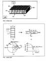
- the high- impedance surface 100includes a lower permittivity spacer layer 104 and a capacitive frequency selective surface (FSS) 102 formed on a metal backplane 106.
- FSScapacitive frequency selective surface
- Metal vias 108extend through the spacer layer 104, and connect the metal backplane to the metal patches of the FSS layer.
- the thickness h of the high impedance surface 100is much less than ⁇ /4 at resonance, and typically on the order of ⁇ /50, as indicated in FIG. 1.
- the FSS 102 of the prior art high impedance surface 100is a periodic array of metal patches 110 which are edge coupled to form an effective sheet capacitance. This is referred to as a capacitive frequency selective surface (FSS).
- Each metal patch 110defines a unit cell which extends through the thickness of the high impedance surface 100.
- Each patch 110is connected to the metal backplane 106, which forms a ground plane, by means of a metal via 108, which can be plated through holes.
- the periodic array of metal vias 108has been known in the prior art as a rodded media, so these vias are sometimes referred to as rods or posts.
- the spacer layer 104 through which the vias 108 passis a relatively low permittivity dielectric typical of many printed circuit board substrates.
- the spacer layer 104is the region occupied by the vias 108 and the low permittivity dielectric.
- the spacer layeris typically 10 to 100 times thicker than the FSS layer 102. Also, the dimensions of a unit cell in the prior art high-impedance surface are much smaller than ⁇ at the fundamental resonance. The period is typically between ⁇ /40 and ⁇ /12.
- a frequency selective surfaceis a two-dimensional array of periodically arranged elements which may be etched on, or embedded within, one or multiple layers of dielectric laminates. Such elements may be either conductive dipoles, patches, loops, or even slots. As a thin periodic structure, it is often referred to as a periodic surface.
- Frequency selective surfaceshave historically found applications in out-of-band radar cross section reduction for antennas on military airborne and naval platforms. Frequency selective surfaces are also used as dichroic subreflectors in dual-band Cassegrain reflector antenna systems. In this application, the subreflector is transparent at frequency band f 1 and opaque or reflective at frequency band f 2 . This allows one to place the feed horn for band f 1 at the focal point for the main reflector, and another feed horn operating at f 2 at the Cassegrain focal point. One can achieve a significant weight and volume savings over using two conventional reflector antennas, which is critical for space-based platforms.
- the prior art high-impedance surface 100provides many advantages.
- the surfaceis constructed with relatively inexpensive printed circuit technology and can be made much lighter than a corrugated metal waveguide, which is typically machined from a block of aluminum.
- the prior art high-impedance surfacecan be 10 to 100 times less expensive for the same frequency of operation.
- the prior art surfaceoffers a high surface impedance for both x and y components of tangential electric field, which is not possible with a corrugated waveguide.
- Corrugated waveguidesoffer a high surface impedance for one polarization of electric field only. According to the coordinate convention used herein, a surface lies in the xy plane and the z-axis is normal or perpendicular to the surface.
- the prior art high-impedance surfaceprovides a substantial advantage in its height reduction over a corrugated metal waveguide, and may be less than one-tenth the thickness of an air-filled corrugated metal waveguide.
- a high-impedance surfaceis important because it offers a boundary condition which permits wire antennas conducting electric currents to be well matched and to radiate efficiently when the wires are placed in very close proximity to this surface (e.g., less than ⁇ /100 away). The opposite is true if the same wire antenna is placed very close to a metal or perfect electric conductor (PEC) surface.
- PECelectric conductor
- the wire antenna/PEC surface combinationwill not radiate efficiently due to a very severe impedance mismatch.
- the radiation pattern from the antenna on a high-impedance surfaceis confined to the upper half space, and the performance is unaffected even if the high-impedance surface is placed on top of another metal surface. Accordingly, an electrically-thin, efficient antenna is very appealing for countless wireless devices and skin-embedded antenna applications.
- FIG. 2illustrates electrical properties of the prior art high-impedance surface.
- FIG. 2(a)illustrates a plane wave normally incident upon the prior art high-impedance surface 100. Let the reflection coefficient referenced to the surface be denoted by ⁇ .
- the physical structure shown in FIG. 2(a)has an equivalent transverse electro-magnetic mode transmission line shown in FIG. 2(b).
- the capacitive FSS 102(FIG. 1) is modeled as a shunt capacitance C and the spacer layer 104 is modeled as a transmission line of length h which is terminated in a short circuit corresponding to the backplane 106.
- Figure 2(c)shows a Smith chart in which the short is transformed into the stub impedance Z stub just below the FSS layer 102.
- the admittance of this stub lineis added to the capacitive susceptance to create a high impedance Z in at the outer surface. Note that the Z in locus on the Smith Chart in FIG. 2(c) will always be found on the unit circle since our model is ideal and lossless. So ⁇ has an amplitude of unity.
- the reflection coefficient ⁇has a phase angle ⁇ which sweeps from 180° at DC, through 0° at the center of the high impedance band, and rotates into negative angles at higher frequencies where it becomes asymptotic to -180°. This is illustrated in FIG. 2(d).
- Resonanceis defined as that frequency corresponding to 0° reflection phase.
- the reflection phase bandwidthis defined as that bandwidth between the frequencies corresponding to the +90° and -90° phases. This reflection phase bandwidth also corresponds to the range of frequencies where the magnitude of the surface reactance exceeds the impedance of free space:
- ⁇ ⁇ o377 ohms.
- a perfect magnetic conductoris a mathematical boundary condition whereby the tangential magnetic field on this boundary is forced to be zero. It is the electromagnetic dual to a perfect electric conductor (PEC) upon which the tangential electric field is defined to be zero.
- PECperfect electric conductor
- a PMCcan be used as a mathematical tool to create simpler but equivalent electromagnetic problems for slot antenna analysis. PMCs do not exist except as mathematical artifacts.
- the prior art high-impedance surfaceis a good approximation to a PMC over a limited band of frequencies defined by the +/-90° reflection phase bandwidth. So in recognition of its limited frequency bandwidth, the prior art high-impedance surface is referred to herein as an example of an artificial magnetic conductor, or AMC.
- an artificial magnetic conductorincludes a frequency selective surface having a frequency dependent permeability ⁇ 1z in a direction normal to the frequency dependent surface, a conductive ground plane, and a rodded medium disposed between the frequency selective surface and the conductive ground plane.
- an artificial magnetic conductorin another aspect, includes a conductive ground plane and a spacer layer disposed on the ground plane.
- One or more arrays of coplanar loopsare resonant at two or more frequency bands, each loop having a similar shape and similar size.
- the one or more arrays of coplanar loopsproduce a frequency dependent normal permeability ⁇ z .
- a disclosed electrical apparatusin another aspect, includes a conductive ground plane and a dielectric layer perforated by conductive rods in electrical contact with the conductive ground plane.
- the electrical apparatusfurther includes a frequency selective surface (FSS) disposed on the dielectric layer.
- the FSSincludes a first layer of capacitively coupled loops resonant at a first frequency, a dielectric spacer layer and a second layer of capacitively coupled loops resonant at a second frequency.
- the frequency selective surfacehas a frequency dependent permeability in a direction substantially normal to the frequency selectively surface.
- a planar, electrically-thin, anisotropic materialis designed to be a high-impedance surface to electromagnetic waves. It is a two-layer, periodic, magnetodielectric structure where each layer is engineered to have a specific tensor permittivity and permeability behavior with frequency. This structure has the properties of an artificial magnetic conductor over a limited frequency band or bands, whereby, near its resonant frequency, the reflection amplitude is near unity and the reflection phase at the surface lies between +/- 90 degrees.
- This engineered materialalso offers suppression of transverse electric (TE) and transverse magnetic (TM) mode surface waves over a band of frequencies near where it operates as a high impedance surface.
- the high impedance surfaceprovides substantial improvements and advantages.
- Advantagesinclude a description of how to optimize the material's effective media constituent parameters to offer multiple bands of high surface impedance. Advantages further include the introduction of various embodiments of conducting loop structures into the engineered material to exhibit multiple reflection-phase resonant frequencies. Advantages still further include a creation of a high-impedance surface exhibiting multiple reflection-phase resonant frequencies without resorting to additional magnetodielectric layers.
- This high-impedance surfacehas numerous antenna applications where surface wave suppression is desired, and where physically thin, readily attachable antennas are desired.
- An artificial magnetic conductoroffers a band of high surface impedance to plane waves, and a surface wave bandgap over which bound, guided transverse electric (TE) and transverse magnetic (TM) modes cannot propagate.
- TE and TM modesare surface waves moving transverse or across the surface of the AMC, in parallel with the plane of the AMC.
- the dominant TM modeis cut off and the dominant TE mode is leaky in this bandgap.
- the bandgapis a band of frequencies over which the TE and TM modes will not propagate as bound modes.
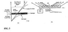
- FIG. 3illustrates surface wave properties of an AMC 300 in proximity to an antenna or radiator 304.
- FIG. 3(a)is an ⁇ - ⁇ diagram for the lowest order TM and TE surface wave modes which propagate on the AMC 300.
- Knowledge of the bandgap over which bound TE and TM waves cannot propagateis very critical for antenna applications of an AMC because it is the radiation from the unbound or leaky TE mode, excited by the wire antenna 304 and the inability to couple into the TM mode that makes bent-wire monopoles, such as the antenna 304 on the AMC 300, a practical antenna element.
- the leaky TE modeoccurs at frequencies only within the bandgap.
- FIG. 3(b)is a cross sectional view of the AMC 300 showing TE waves radiating from the AMC 300 as leaky waves. Leakage is illustrated by the exponentially increasing spacing between the arrows illustrating radiation from the surface as the waves radiate power away from the AMC 300 near the antenna 304. Leakage of the surface wave dramatically reduces the diffracted energy from the edges of the AMC surface in antenna applications.
- the radiation pattern from small AMC ground planescan therefore be substantially confined to one hemisphere, the hemisphere above the front or top surface of the AMC 300.
- the front or top surfaceis the surface proximate the antenna 304.
- the hemisphere below or behind the AMC 300, below the rear or bottom surface of the AMC 300is essentially shielded from radiation.
- the rear or bottom surface of the AMC 300is the surface away from the antenna 304.
- FIG. 4illustrates a TE surface wave mode on the artificial magnetic conductor 300 of FIG. 3.
- FIG. 5illustrates a TM surface wave mode on the AMC 300 of FIG. 3.
- the z axisis normal to the surface.
- the TE mode of FIG. 4propagates in the x direction along with loops of an associated magnetic field H.
- the amplitude of the x component of magnetic field H both above the surface and within the surfaceis shown by the graph in FIG. 4.
- FIG. 5shows the TM mode propagating in the x direction, along with loops of an associated electric field E.
- the relative amplitude of the x component of the electric field Eis shown in the graph in FIG. 5.
- An effective media modelallows transformation all of the fine, detailed, physical structure of an AMC's unit cell into that of equivalent media defined only by the permittivity and permeability parameters. These parameters allow use of analytic methods to parametrically study wave propagation on AMCs. Such analytic models lead to physical insights as to how and why AMCs work, and insights on how to improve them. They allow one to study an AMC in general terms, and then consider each physical embodiment as a specific case of this general model. However, it is to be noted that such models represent only approximations of device and material performance and are not necessarily precise calculations of that performance.
- a prior art high-impedance surface 100comprised of a square lattice of square patches 110 as illustrated in FIG. 6.
- Each patch 110has a metal via 108 connecting it to the backplane 106.
- the via 108passes through a spacer layer 102, whose isotropic host media parameters are ⁇ D and ⁇ D .
- FIG. 7presents a new effective media model for substantially characterizing the prior art high-impedance surface of FIG. 6.
- Elements of the permittivity tensorare given in FIG. 7.
- Each unit cellhas an area A and includes one patch 110, measuring b x b in size, plus the space g in the x and y directions to an adjacent patch 110, for a pitch or period of a , and with a thickness equal to the thickness of the high impedance surface 100, or h + ⁇ in FIG. 6.
- ⁇is typically a small number much less than unity, and usually below 1%.
- the high impedance surface 100includes a first or upper region 602 and a second or lower region 604.
- the lower region 604, denoted here as region 2is referred to as a rodded media.
- Transverse electric and magnetic fields in this region 604are only minimally influenced by the presence of the vias or rods 108.
- the effective transverse permittivity, ⁇ 2 x and permeability, ⁇ 2 xare calculated as minor perturbations from the media parameters of the host dielectric. This is because the electric polarisability of a circular cylinder, ⁇ d 2 /2, is quite small for the thin metal rods whose diameter is small relative to the period a .
- the upper region 602is a capacitive FSS.
- the effective sheet capacitance, C⁇ o ⁇ 1 x t , is uniquely defined by the geometry of each patch 110, but ⁇ 1 x in the effective media model is somewhat arbitrary since t is chosen arbitrarily.
- the variable tis not necessarily the thickness of the patches, which is denoted as ⁇ . However, t should be much less than the spacer layer 604 height h .
- An artificial magnetic moleculeis an electrically small conductive loop which typically lies in one plane. Both the loop circumference and the loop diameter are much less than one free-space wavelength at the useful frequency of operation.
- the loopscan be circular, square, hexagonal, or any polygonal shape, as only the loop area will affect the magnetic dipole moment.
- the loopsare loaded with series capacitors to force them to resonate at frequencies well below their natural resonant frequency
- a three dimensional, regular array or lattice of AMMsis an artificial material whose permeability can exhibit a Lorentz resonance, assuming no intentional losses are added. At a Lorentz resonant frequency, the permeability of the artificial material approaches infinity.
- the array of moleculescan behave as a bulk paramagnetic material ( ⁇ r > 1) or as a diamagnetic material ( ⁇ r ⁇ 1 ) in the direction normal to the loops.
- AMMsmay be used to depress the normal permeability of the FSS layer, region 1, in AMCs. This in turn has a direct impact on the TE mode cutoff frequencies, and hence the surface wave bandgaps.
- a prior art high impedance surface designed to operate at low microwave frequencies (1-3 GHz)will typically exhibit its next reflection phase resonance in millimeter wave bands (above 30 GHz).
- an AMCwhich provides a second band or even multiple bands of high surface impedance whose resonant frequencies are all relatively closely spaced, within a ratio of about 2:1 or 3:1. This is needed, for example, for multi-band antenna applications. Furthermore, there is a need for an AMC with sufficient engineering degrees of freedom to allow the second and higher reflection phase resonances to be engineered or designated arbitrarily. Multiple reflection phase resonances are possible if more than two layers (4, 6, 8, etc.) are used in the fabrication of an AMC. However, this adds cost, weight, and thickness relative to the single resonant frequency design. Thus there is a need for a means of achieving multiple resonances from a more economical two-layer design. In addition, there is a need for a means of assuring the existence of a bandgap for bound, guided, TE and TM mode surface waves for all of the high-impedance bands, and within the +/- 90° reflection phase bandwidths.
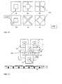
- FIG. 8illustrates an artificial magnetic conductor (AMC) 800.
- the AMC 800includes an array 802 that is in one embodiment a coplanar array of resonant loops or artificial magnetic molecules 804 which are strongly capacitively coupled to each other, forming a capacitive frequency selective surface (FSS).
- the resonant loops 804 in the illustrated embodimentare uniformly spaced and at a height h above a solid conductive ground plane 806.
- An array of electrically short, conductive posts or vias 808are attached to the ground plane 806 only and have a length h .
- Each loop 804includes a lumped capacitive load 810.
- the one or more layers of artificial magnetic molecules (AMMs) or resonant loops of the artificial magnetic conductor 800create a frequency dependent permeability in the z direction, normal to the surface of the AMC 800.
- each loop and capacitor loadare substantially identical so that all loops have substantially the same resonant frequency.
- loops having different characteristicsmay be used. In physical realizations, due to manufacturing tolerances and other causes, individual loops and their associated resonant frequencies will not necessarily be identical.
- FIG. 10is a cross sectional view of the artificial magnetic conductor 900 of FIG. 9.
- the AMC 900includes a first layer 902 of loops 804 resonant at a first frequency f 1 .
- the AMC 900includes a second layer 904 of loops 804 resonant at a second frequency f 2 .
- Each loop 804 of the first layer 902 of loopsincludes a lumped capacitive load C 1 908.
- Each loop 804 of the second layer 904 of loopsincludes a lumped capacitive load C 2 906.
- the lumped capacitancesmay be the same but need not be.
- the first layer 902 of loops 804 and the second layer 906 of loops 904form a frequency selective surface (FSS) layer 910 disposed on a spacer layer 912.
- FSSfrequency selective surface
- the low frequency limit of the transverse effective relative permittivity, ⁇ 1x and ⁇ 1ylies between 100 and 2000. Accordingly, strong capacitive coupling is present between loops 902 and 904.
- a practical way to achieve this couplingis to print two layers of loops on opposite sides of an FSS dielectric layer as shown in FIG. 10. Other realizations may be chosen as well.
- FIG. 11illustrates a first physical embodiment of a loop 1100 for use in an artificial magnetic conductor such as the AMC 800 of FIG. 8.
- Conducting loopssuch as loop 1100 which form the artificial magnetic molecules can be implemented in a variety of shapes such as square, rectangular, circular, triangular, hexagonal, etc.
- the loop 1100is square in shape.
- Notches 1102can be designed in the loops to increase the self inductance, which lowers the resonant frequency of the AMMs.
- Notches 1102 and gaps 1104can also be introduced to engineer the performance of the loop 1100 to a particular desired response. For example, the bands or resonance frequencies may be chosen by selecting a particular shape for the loop 1100.
- a gap 1104cuts all the way through a side of the loop 1100 from the center of the loop 1100 to the periphery.
- a notchcuts through only a portion of a side between the center and periphery of the loop 1100.
- FIG. 11illustrates a selection of potential square loop designs.
- FIG. 12illustrates a portion of a two layer artificial magnetic conductor whose FSS layer uses a square loop of FIG. 11(d). Wide loops with relatively large surface area promote capacitive coupling between loops of adjacent layers when used in a two-layer overlapping AMC, as illustrated in FIG. 12. An overlap region 1202 at the gap 1104 provides the series capacitive coupling required for loop resonance.
- loops of the type illustrated in FIGS. 11 and 12are formed on surfaces of dielectric materials using conventional printed circuit board (PCB) manufacturing techniques.
- PCBprinted circuit board
- a metallic layeris deposited on a surface of the PCB and subsequently patterned by chemical etching or other technique. Such processes provide precise control of sizes, spacing and uniformity of printed features.
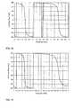
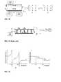
- FIG. 13 and FIG. 14show simulation results for the normal-incidence reflection phase of the AMC illustrated in FIG. 12.
- the incident electric fieldis y-polarized.
- FIG. 13shows a fundamental resonance near 1.685 GHz, and a second resonance near 2.8 GHz.
- the reason that the AMC 800 with gaps 1104 has a second resonanceis that the effective transverse permittivity of the frequency selective surface has become frequency dependent.
- a simple capacitive modelis no longer adequate.
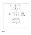
- FIG. 15shows equivalent circuits for portions of the artificial magnetic conductor 800 of FIG. 8.
- FIG. 15(a)illustrates the second Foster canonical form for the input admittance of a one-port circuit, which is a general analytic model for the effective transverse permittivity of complex frequency selective surface (FSS) structures.
- FIG. 15(b)gives an example of a specific equivalent circuit model for an FSS whereby two material or intrinsic resonances are assumed.
- FIG. 15(c)shows the TEM mode equivalent circuit for plane waves normally incident on a two layer AMC, such as AMC 900 of FIG. 9.
- the models developed hereinare useful for characterizing, understanding, designing and engineering devices such as the AMCs described and illustrated herein. These models represent approximations of actual device behavior.
- Complex loop FSS structuressuch as that shown in FIG. 12, have a dispersive, or frequency dependent, effective transverse permittivity which can be properly modeled using a more complex circuit model. Furthermore, analytic circuit models for dispersive dielectric media can be extended in applicability to model the transverse permittivity of complex FSS structures.
- the second Foster canonical circuit for one-port networks, shown in FIG. 15(a),is a general case which should cover all electrically-thin FSS structures. Each branch manifests an intrinsic resonance of the FSS. For an FSS made from low loss materials, R n is expected to be very low, hence resonances are expected to be Lorentzian.
- the effective sheet capacitance for the loop FSS shown in FIG. 12has a Lorentz resonance somewhere between 1.685 GHz and 2.8 GHz.
- the ⁇ 1 y curve 1602 shown in the upper graph of FIG. 16is obtained.
- Two FSS material resonancesare evident near 2.25 GHz and 3.2 GHz.
- the ⁇ 1 y curve 1604is the transverse relative permittivity required to achieve resonance for the AMC, a zero degree reflection phase.
- the reflection phase curve shown in the lower graph of FIG. 16was computed using the transmission line model shown in FIG.
- FIGS. 17, 20 and 21There are many additional square loop designs which may be implemented in FSS structures to yield a large transverse effective permittivity. More examples are shown in FIGS. 17, 20 and 21 where loops of substantially identical size and similar shape are printed on opposite sides of a single dielectric layer FSS. Reflection phase results for x and y polarized electric fields applied to an AMC of the design shown in FIG. 17 are shown in FIGS. 18 and 19.
- P400 mils
- g130 mils
- g220 mils
- r40 mils
- w30 mils
- t8 mils
- h60 mils.
- ⁇ r3.38 in both FSS and spacer layers since this printed AMC is fabricated using Rogers R04003 substrate material.
- a viais fabricated using a 20 mil diameter plated through hole.
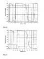
- FIG. 18shows measured reflection phase data for an x polarized electric field normally incident on the AMC of FIG. 17. Resonant frequencies are observed near 1.6 GHz and 3.45 GHz.
- FIG. 19shows measured reflection phase data for a y polarized electric field normally incident on the AMC of FIG. 17. Resonant frequencies are observed near 1.4 GHz and 2.65 GHz.
- each polarizationsees different resonant frequencies. However, it is believed that the design has sufficient degrees of freedom to make the resonance frequencies polarization independent.
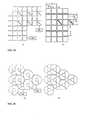
- FIG. 21shows an additional alternative embodiment for a frequency selective surface implemented with square loops.
- the illustrated loop design of FIG. 21has overlapping square loops 2100 on each layer 902, 904 with deep notches 2102 cut from the center 2104 toward each corner. Gaps 2106, 2108 are found at the 4:30 position on the upper layer and at the 7:30 position on the lower layer respectively.
- AMC reflection phase for the x and y directed E field polarizationis shown in FIGS. 22 and 23 respectively. Again, dual resonant frequencies are clearly seen.
- FIG. 24An alternative type of dispersive capacitive FSS structure can be created where loops 2402 are printed on the one side and notched patches 2404 are printed on the other side of a single dielectric layer FSS. An example is shown in FIG. 24.
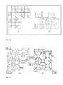
- hexagonal loopscan be printed in a variety of shapes that include notches which increase the loop self inductance. These notches may vary in number and position, and they are not necessarily the same size in a given loop. Furthermore, loops printed on opposite sides of a dielectric layer can have different sizes and features. There are a tremendous number of independent variables which uniquely define a multilayer loop FSS structure.
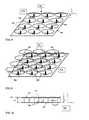
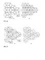
- FIGS. 25, 26 and 27Six possibilities of hexagonal loop FSS designs are illustrated in FIGS. 25, 26 and 27.
- a first layer 902 of loopsis capacitively coupled with a second layer of loops 904.
- the hexagonal loops presented hereare intended to be regular hexagons. Distorted hexagons could be imagined in this application, but their advantage is unknown at this time.
- FIG. 28illustrates an effective media model for a high impedance surface 2800.
- the general effective media model of FIG. 28is applicable to high impedance surfaces such as the prior art high impedance surface 100 of FIG. 1 and the artificial magnetic conductor (AMC) 800 of FIG. 8.
- the AMC 800includes two distinct electrically-thin layers, a frequency selective surface (FSS) 802 and a spacer layer 804.
- Each layer 802, 804is a periodic structure with a unit cell repeated periodically in both the x and y directions.
- the periods of each layer 802, 804are not necessarily equal or even related by an integer ratio, although they may be in some embodiments.
- the period of each layeris much smaller than a free space wavelength ⁇ at the frequency of analysis ( ⁇ /10 or smaller).
- the effective media modeldoes not necessarily characterize precisely the performance or attributes of a surface such as the AMC 800 of FIG. 8 but merely models the performance for engineering and analysis. Changes may be made to aspects of the effective media model without altering the overall effectiveness of the model or the benefits obtained therefrom.
- the high impedance surface 2800 for the AMC 800 of FIG. 8is characterized by an effective media model which includes an upper layer and a lower layer, each layer having a unique tensor permittivity and tensor permeability.
- Each layer's tensor permittivity and each layer's tensor permeabilityhave non-zero elements on the main tensor diagonal only, with the x and y tensor directions being in-plane with each respective layer and the z tensor direction being normal to each layer.
- the result for the AMC 800is an AMC resonant at multiple resonance frequencies.
- each layer 2802, 2804is a bi-anisotropic media, meaning both permeability ⁇ and permittivity ⁇ are tensors. Further, each layer 2802, 2804 is uniaxial meaning two of the three main diagonal components are equal, and off-diagonal elements are zero, in both ⁇ and ⁇ . So each layer 2802, 2804 may be considered a bi-uniaxial media.
- the subscripts t and ndenote the transverse ( x and y directions) and normal ( z direction) components.
- Each of the two layers 2802, 2804 in the bi-uniaxial effective media model for the high impedance surface 2800has four material parameters: the transverse and normal permittivity, and the transverse and normal permeability.
- the transverse and normal permittivityGiven two layers 2802, 2804, there are a total of eight material parameters required to uniquely define this model. However, any given type of electromagnetic wave will see only a limited subset of these eight parameters. For instance, uniform plane waves at normal incidence, which are a transverse electromagnetic (TEM) mode, are affected by only the transverse components of permittivity and permeability.
- TEMtransverse electromagnetic
- a transverse electric (TE) surface wave propagating on the high impedance surface 2800has a field structure shown in FIG. 4.
- the electric field (E field)is transverse to the direction of wave propagation, the + x direction. It is also parallel to the surface. So the electric field sees only transverse permittivities.
- the magnetic field (H field) linesform loops in the xz plane which encircle the E field lines. So the H field sees both transverse and normal permeabilities.
- the transverse magnetic (TM) surface wavehas a field structure shown in FIG. 5. Note that, for TM waves, the role of the E and H fields is reversed relative to the TE surface waves. For TM modes, the H field is transverse to the direction of propagation, and the E field lines (in the xz plane) encircle the H field. So the TM mode electric field sees both transverse and normal permittivities.
- ⁇ 1 n and ⁇ 2 nare fundamental parameters which permit independent control of the TM modes, and hence the dominant TM mode cutoff frequency.
- ⁇ 1 n and ⁇ 2 nare fundamental parameters which permit independent control of the TE modes, and hence the dominant TE mode cutoff frequency.
- FIG. 29shows a prior art high impedance surface 100 whose frequency selective surface 102 is a coplanar layer of square conductive patches of size b x b, separated by a gap of dimension g..
- ⁇ Dis the relative permittivity of the background or host dielectric media in the spacer layer 104
- ⁇ Dis the relative permeability of this background media in the spacer layer 104
- ⁇is the ratio of cross sectional area of each rod or post to the area A of the unit cell in the rodded media or spacer layer 104.
- Cdenotes the fixed FSS sheet capacitance.
- the rods or postsmay be realized by any suitable physical embodiment, such as plated-through holes or vias in a conventional printed circuit board or by wires inserted through a foam. Any technique for creating a forest of vertical conductors (i.e., parallel to the z axis), each conductor being electrically coupled with the ground plane, may be used.
- the conductors or rodsmay be circular in cross section or may be flat strips of any cross section whose dimensions are small with respect to the wavelength ⁇ in the host medium or dielectric of the spacer layer. In this context, small dimensions for the rods are generally in the range of ⁇ /1000 to ⁇ /25.
- the AMC 800has transverse permittivity in the y tensor direction substantially equal to the transverse permittivity in the x tensor direction. This yields an isotropic high impedance surface in which the impedance along the y axis is substantially equal to the impedance along the x axis.
- the transverse permittivity in the y tensor directiondoes not equal the transverse permittivity in the x tensor direction to produce an anisotropic high impedance surface, meaning the impedances along the two inplane axes are not equal. Examples of the latter are shown in Figures 17 and 21.
- Effective media models for substantially modelling both the high impedance surface 100 and an AMC 800, 900are listed in Table 2. Two of the tensor elements are distinctly different in the AMC 800, 900 relative to the prior art high-impedance surface 100. These are the transverse permittivity ⁇ 1 x , ⁇ 1 y and the normal permeability ⁇ 1 z , both of the upper layer or frequency selective surface. The model for the lower layer or spacer layer is the same in both the high impedance surface 100 and the AMC 800, 900.
- Y ( ⁇ )is an admittance function written in the second Foster canonical form for a one port circuit:
- the high impedance surface 100has an FSS capacitance which is frequency independent.
- the AMC 800, 900has an FSS 802 whose capacitance contains inductive elements in such a way that the sheet capacitance undergoes one or more Lorentz resonances at prescribed frequencies. Such resonances are accomplished by integrating into the FSS 802 the physical features of resonant loop structures, also referred to as artificial magnetic molecules. As the frequency of operation is increased, the capacitance of the FSS 802 will undergo a series of abrupt changes in total capacitance.
- FIG. 30illustrates sheet capacitance for the frequency selective surface 802 of the AMC 800 of FIG. 8 and the AMC 900 of FIG. 9.
- FIG. 30(a)shows that the capacitance of the FSS 802 is frequency dependent.
- FIG 30(b)shows a Debye response obtained from a lossy FSS where R n is significant.
- the drop in capacitance across each resonant frequencyis equal to C n , the capacitance in each shunt branch of Y ( ⁇ ).
- This FSS capacitanceis used to tune the inductance of the spacer layer 804, which is a constant, to achieve a resonance in the reflection coefficient phase for the AMC 800, 900.
- This multi-valued FSS capacitance as a function of frequencyis the mechanism by which multiple bands of high surface impedance are achieved for the AMC 800, 900.
- the two-layer high impedance surface 100will offer reflection phase resonances at a fundamental frequency, plus higher frequencies near where the electrical thickness of the bottom layer is n ⁇ and n is an integer. These higher frequency resonances are approximately harmonically related, and hence uncontrollable.
- a second difference in the tensor effective media properties for the high impedance surface 100 and AMC 800is in the normal permeability component ⁇ 1 n .
- the high impedance surface 100has a constant ⁇ 1 n
- the AMC 800, 900is designed to have a frequency dependent ⁇ 1 n .
- the impedance function Z ( ⁇ )can be written in the first Foster canonical form for a one-port circuit.
- This impedance functionis sufficient to accurately describe the normal permeability of the FSS 802 in an AMC 800, 900 regardless of the number and orientation of uniquely resonant artificial magnetic molecules.
- the prior art high-impedance surface 100whose FSS 102 is composed of metal patches, has a lower bound for ⁇ 1 n .
- This lower boundis inversely related to the transverse permittivity according to the approximate relation ⁇ 1 n ⁇ 2/ ⁇ 1 t .
- ⁇ 1 nis anchored at this value for the prior art high- impedance surface 100.
- the overlapping loops used in the FSS 802 of the AMC 800, 900allow independent control of the normal permeability. Normal permeabilities may be chosen so that surface wave suppression occurs over some and possibly all of the +/- 90° reflection phase bandwidths in a multi-band AMC such as AMC 800 and AMC 900.
- the illustrated embodimentuses arrays of overlapping loops as the FSS layer 802, or in conjunction with a capacitive FSS layer, tuned individually or in multiplicity with a capacitance. This capacitance may be the self capacitance of the loops, the capacitance offered by adjacent layers, or the capacitance of external capacitors attached to the FSS. such as chip capacitors.
- the loops and capacitanceare tuned so as to obtain a series of Lorentz resonances across the desired bands of operation.
- the resonances of the artificial magnetic moleculesaffords the designer a series of staircase steps of progressively dropping normal permeability.
- the region of rapidly changing normal permeability around the resonancesmay be used to advantage in narrowband operations.
- the illustrated embodimentuses plateaus of extended depressed normal permeability to suppress the onset of guided bound TE surface waves within the desired bands of high-impedance operation.
- the purpose of the resonance in the effective transverse permittivities ⁇ 1 tis to provide multiple bands of high surface impedance.
- the purpose of the resonances in the normal permeability ⁇ 1 nis to depress its value so as to prevent the onset of TE modes inside the desired bands of high impedance operation.
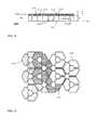
- FIG. 31illustrates an artificial magnetic conductor 3100 including a multiple layer frequency selective surface (FSS) 3102.
- the AMC 3100further includes a conductive ground plane 3104 and a rodded media forming a spacer layer 3106 disposed between the FSS 3102 and the conductive ground plane 3104.
- the FSS 3102has a frequency dependent permeability ⁇ 1z in a direction normal to the frequency dependent surface 3102. Exemplary dimensions and coordinate axes are shown in FIG. 31.
- the FSS 3102includes three arrays of substantially coplanar artificial magnetic molecules.
- the artificial magnetic moleculesare preferably implemented as overlapping capacitively coupled loops.
- the FSS 3102includes a first array 3112, a second array 3114 and a third array 3116 of artificial magnetic molecules.
- a first dielectric layer 3118separates the first array 3112 of artificial magnetic molecules from the second array 3114 of artificial magnetic molecules.
- the arrays 3112, 3114, 3116are shown as being coplanar in respective planes. This arrangement is particularly well suited to manufacture using conventional printed circuit board (PCB) manufacturing techniques of depositing a metallic layer on a PCB surface and etching with a chemical or other process. In other embodiments, other manufacturing techniques, some of which will produce arrays of artificial magnetic molecules which are not substantially coplanar, may be substituted.
- PCBprinted circuit board
- the AMC 3100includes three layers 3112, 3114, 3116 of loops separated by two dielectric layers 3118, 3120. In other embodiments, other combinations of layers of loops and dielectric layers may be used.
- a FSS in accordance with the disclosed embodimentswill include n layers of loops and n-1 dielectric layers isolating the layers of loops.
- the spacer layer 3106includes metallic rods 3108 periodically positioned in a dielectric material.
- each loop of each array of loops 3112, 3114, 3116is associated with a rod 3108 of the spacer layer 3106.
- Any suitable manufacturing methodfor example, as described above, may be used to manufacture the rodded media of the spacer layer 3108.
- FIG. 32illustrates a top view of the multiple-layer frequency selective surface 3102 of FIG. 31.
- FIG. 32shows the first array 3112, the second array 3114 and the third array 3116 of the frequency selective surface 3102. A portion only of each array is visible to illustrate the layering of the respective arrays.
- each of the arrays 3112, 3114, 3116includes substantially identical hexagonal loops periodically spaced on the FSS 3102. Each loop is notched to tailor the self-inductance of the loop and includes a gap to tailor the resonant frequency of the loop.
- the embodiment of FIGS. 31 and 32is illustrative only. In other embodiments, different size and shape loops may be used along with different numbers of layers or arrays.
- the present embodimentsprovide a variety of high-impedance surfaces or artificial magnetic conductors which exhibit multiple reflection phase resonances, or multi-band performance.
- the resonant frequencies for high surface impedanceare not harmonically related, but occur at frequencies which may be designed or engineered. This is accomplished by designing the tensor permittivity of the upper layer to have a behavior with frequency which exhibits one or more Lorentzian resonances.
Landscapes
- Physics & Mathematics (AREA)
- Optics & Photonics (AREA)
- Aerials With Secondary Devices (AREA)
- Details Of Aerials (AREA)
- Waveguide Aerials (AREA)
Abstract

Description
This application is a continuation in part of application serial number 09/678, 128 filed October 4, 2000 and commonly assigned with the present application.
The present invention relates generally to high-impedance surfaces. Moreparticularly, the present invention relates to a multi-resonant, high-impedanceelectromagnetic surface.
A high impedance surface is a lossless, reactive surface whose equivalentsurface impedance,Zs =Etan /Htan, approximates an open circuit and which inhibitsthe flow of equivalent tangential electric surface current, thereby approximating azero tangential magnetic field,Htan ≈ 0.Etan andHtan are the electric andmagnetic fields, respectively, tangential to the surface. High impedance surfaceshave been used in various antenna applications. These applications range fromcorrugated horns which are specially designed to offer equal E and H plane halfpower beamwidths to traveling wave antennas in planar or cylindrical form.However, in these applications, the corrugations or troughs are made of metalwhere the depth of the corrugations is one quarter of a free space wavelength, λ/4,where λ is the wavelength at the frequency of interest. At high microwavefrequencies, λ/4 is a small dimension, but at ultra-high frequencies (UHF, 300MHz to 1 GHz), or even at low microwave frequencies (1-3 GHz), λ/4 can bequite large. For antenna applications in these frequency ranges, an electrically-thin(λ/100 to λ/50 thick) and physically thin high impedance surface is desired.
One example of a thin high-impedance surface is disclosed in D.Sievenpiper, "High-impedance electromagnetic surfaces," Ph.D. dissertation,UCLA electrical engineering department, filed January 1999, and in PCT Patent Application number PCT/US99/06884. Thishigh impedance surface 100 isshown in FIG. 1. The high-impedance surface 100 includes a lowerpermittivityspacer layer 104 and a capacitive frequency selective surface (FSS) 102 formed onametal backplane 106.Metal vias 108 extend through thespacer layer 104, andconnect the metal backplane to the metal patches of the FSS layer. The thicknessh of thehigh impedance surface 100 is much less than λ/4 at resonance, andtypically on the order of λ/50, as indicated in FIG. 1.
The FSS 102 of the prior arthigh impedance surface 100 is a periodic arrayofmetal patches 110 which are edge coupled to form an effective sheetcapacitance. This is referred to as a capacitive frequency selective surface (FSS).Eachmetal patch 110 defines a unit cell which extends through the thickness ofthehigh impedance surface 100. Eachpatch 110 is connected to themetalbackplane 106, which forms a ground plane, by means of a metal via 108, whichcan be plated through holes. The periodic array ofmetal vias 108 has been knownin the prior art as a rodded media, so these vias are sometimes referred to as rodsor posts. Thespacer layer 104 through which thevias 108 pass is a relatively lowpermittivity dielectric typical of many printed circuit board substrates. Thespacerlayer 104 is the region occupied by thevias 108 and the low permittivitydielectric. The spacer layer is typically 10 to 100 times thicker than theFSS layer 102. Also, the dimensions of a unit cell in the prior art high-impedance surfaceare much smaller than λ at the fundamental resonance. The period is typicallybetween λ/40 and λ/12.
A frequency selective surface is a two-dimensional array of periodicallyarranged elements which may be etched on, or embedded within, one or multiplelayers of dielectric laminates. Such elements may be either conductive dipoles,patches, loops, or even slots. As a thin periodic structure, it is often referred to asa periodic surface.
Frequency selective surfaces have historically found applications in out-of-bandradar cross section reduction for antennas on military airborne and navalplatforms. Frequency selective surfaces are also used as dichroic subreflectors in dual-band Cassegrain reflector antenna systems. In this application, thesubreflector is transparent at frequency band f1 and opaque or reflective atfrequency band f2. This allows one to place the feed horn for band f1 at the focalpoint for the main reflector, and another feed horn operating at f2 at the Cassegrainfocal point. One can achieve a significant weight and volume savings over usingtwo conventional reflector antennas, which is critical for space-based platforms.
The prior art high-impedance surface 100 provides many advantages. Thesurface is constructed with relatively inexpensive printed circuit technology andcan be made much lighter than a corrugated metal waveguide, which is typicallymachined from a block of aluminum. In printed circuit form, the prior art high-impedancesurface can be 10 to 100 times less expensive for the same frequencyof operation. Furthermore, the prior art surface offers a high surface impedancefor both x and y components of tangential electric field, which is not possible witha corrugated waveguide. Corrugated waveguides offer a high surface impedancefor one polarization of electric field only. According to the coordinate conventionused herein, a surface lies in the xy plane and the z-axis is normal or perpendicularto the surface. Further, the prior art high-impedance surface provides a substantialadvantage in its height reduction over a corrugated metal waveguide, and may beless than one-tenth the thickness of an air-filled corrugated metal waveguide.
A high-impedance surface is important because it offers a boundarycondition which permits wire antennas conducting electric currents to be wellmatched and to radiate efficiently when the wires are placed in very closeproximity to this surface (e.g., less than λ/100 away). The opposite is true if thesame wire antenna is placed very close to a metal or perfect electric conductor(PEC) surface. The wire antenna/PEC surface combination will not radiateefficiently due to a very severe impedance mismatch. The radiation pattern fromthe antenna on a high-impedance surface is confined to the upper half space, andthe performance is unaffected even if the high-impedance surface is placed on topof another metal surface. Accordingly, an electrically-thin, efficient antenna is very appealing for countless wireless devices and skin-embedded antennaapplications.
FIG. 2 illustrates electrical properties of the prior art high-impedancesurface. FIG. 2(a) illustrates a plane wave normally incident upon the prior arthigh-impedance surface 100. Let the reflection coefficient referenced to thesurface be denoted by Γ. The physical structure shown in FIG. 2(a) has anequivalent transverse electro-magnetic mode transmission line shown in FIG. 2(b).The capacitive FSS 102 (FIG. 1) is modeled as a shunt capacitance C and thespacer layer 104 is modeled as a transmission line of lengthh which is terminatedin a short circuit corresponding to thebackplane 106. Figure 2(c) shows a Smithchart in which the short is transformed into the stub impedanceZstub just belowtheFSS layer 102. The admittance of this stub line is added to the capacitivesusceptance to create a high impedanceZin at the outer surface. Note that theZinlocus on the Smith Chart in FIG. 2(c) will always be found on the unit circle sinceour model is ideal and lossless. So Γ has an amplitude of unity.
The reflection coefficient Γ has a phase angle which sweeps from 180°at DC, through 0° at the center of the high impedance band, and rotates intonegative angles at higher frequencies where it becomes asymptotic to -180°. Thisis illustrated in FIG. 2(d). Resonance is defined as that frequency correspondingto 0° reflection phase. Herein, the reflection phase bandwidth is defined as thatbandwidth between the frequencies corresponding to the +90° and -90° phases.This reflection phase bandwidth also corresponds to the range of frequencieswhere the magnitude of the surface reactance exceeds the impedance of free space:|X| ≥ ηo = 377 ohms.
A perfect magnetic conductor (PMC) is a mathematical boundary conditionwhereby the tangential magnetic field on this boundary is forced to be zero. It isthe electromagnetic dual to a perfect electric conductor (PEC) upon which thetangential electric field is defined to be zero. A PMC can be used as amathematical tool to create simpler but equivalent electromagnetic problems forslot antenna analysis. PMCs do not exist except as mathematical artifacts. However, the prior art high-impedance surface is a good approximation to a PMCover a limited band of frequencies defined by the +/-90° reflection phasebandwidth. So in recognition of its limited frequency bandwidth, the prior arthigh-impedance surface is referred to herein as an example of an artificialmagnetic conductor, or AMC.
The prior art high-impedance surface offers reflection phase resonances ata fundamental frequency, plus higher frequencies approximated by the conditionwhere the electrical thickness of the spacer layer,βh, in the high-impedancesurface 100 isnπ, where n is an integer. These higher frequency resonances areharmonically related and hence uncontrollable. If the prior art AMC is to be usedin a dual-band antenna application where the center frequencies are separated by afrequency range of, say 1.5:1, we would be forced to make a very thick AMC.Assuming a non-magnetic spacer layer (µD =1), the thicknessh must be h=λ/14to achieve at least a 50% fractional frequency bandwidth where both centerfrequencies would be contained in the reflection phase bandwidth. Alternatively,magnetic materials could be used to load the spacer layer, but this is a topic ofongoing research and nontrivial expense. Accordingly, there is a need for a classof AMCs which exhibit multiple reflection phase resonances, or multi-bandperformance, that are not harmonically related, but at frequencies which may beprescribed.
By way of introduction only, in a first aspect, an artificial magneticconductor includes a frequency selective surface having a frequency dependentpermeability µ1z in a direction normal to the frequency dependent surface, aconductive ground plane, and a rodded medium disposed between the frequencyselective surface and the conductive ground plane.
In another aspect, an artificial magnetic conductor includes a conductiveground plane and a spacer layer disposed on the ground plane. One or more arraysof coplanar loops are resonant at two or more frequency bands, each loop having a similar shape and similar size. The one or more arrays of coplanar loops producea frequency dependent normal permeability µz.
In another aspect, a disclosed electrical apparatus includes a conductiveground plane and a dielectric layer perforated by conductive rods in electricalcontact with the conductive ground plane. The electrical apparatus furtherincludes a frequency selective surface (FSS) disposed on the dielectric layer. TheFSS includes a first layer of capacitively coupled loops resonant at a firstfrequency, a dielectric spacer layer and a second layer of capacitively coupledloops resonant at a second frequency. The frequency selective surface has afrequency dependent permeability in a direction substantially normal to thefrequency selectively surface.
The foregoing summary has been provided only by way of introduction.Nothing in this section should be taken as a limitation on the following claims,which define the scope of the invention.
A planar, electrically-thin, anisotropic material is designed to be a high-impedancesurface to electromagnetic waves. It is a two-layer, periodic,magnetodielectric structure where each layer is engineered to have a specifictensor permittivity and permeability behavior with frequency. This structure hasthe properties of an artificial magnetic conductor over a limited frequency band orbands, whereby, near its resonant frequency, the reflection amplitude is near unityand the reflection phase at the surface lies between +/- 90 degrees. This engineeredmaterial also offers suppression of transverse electric (TE) and transverse magnetic (TM) mode surface waves over a band of frequencies near where itoperates as a high impedance surface. The high impedance surface providessubstantial improvements and advantages. Advantages include a description ofhow to optimize the material's effective media constituent parameters to offermultiple bands of high surface impedance. Advantages further include theintroduction of various embodiments of conducting loop structures into theengineered material to exhibit multiple reflection-phase resonant frequencies.Advantages still further include a creation of a high-impedance surface exhibitingmultiple reflection-phase resonant frequencies without resorting to additionalmagnetodielectric layers.
This high-impedance surface has numerous antenna applications wheresurface wave suppression is desired, and where physically thin, readily attachableantennas are desired. This includes internal antennas in radiotelephones and inprecision GPS antennas where mitigation of multipath signals near the horizon isdesired.
An artificial magnetic conductor (AMC) offers a band of high surfaceimpedance to plane waves, and a surface wave bandgap over which bound, guidedtransverse electric (TE) and transverse magnetic (TM) modes cannot propagate.TE and TM modes are surface waves moving transverse or across the surface ofthe AMC, in parallel with the plane of the AMC. The dominant TM mode is cutoff and the dominant TE mode is leaky in this bandgap. The bandgap is a band offrequencies over which the TE and TM modes will not propagate as bound modes.
FIG. 3 illustrates surface wave properties of anAMC 300 in proximity toan antenna orradiator 304. FIG. 3(a) is an ω-β diagram for the lowest order TMand TE surface wave modes which propagate on theAMC 300. Knowledge ofthe bandgap over which bound TE and TM waves cannot propagate is very criticalfor antenna applications of an AMC because it is the radiation from the unboundor leaky TE mode, excited by thewire antenna 304 and the inability to couple intothe TM mode that makes bent-wire monopoles, such as theantenna 304 on theAMC 300, a practical antenna element. The leaky TE mode occurs at frequenciesonly within the bandgap.
FIG. 3(b) is a cross sectional view of theAMC 300 showing TE wavesradiating from theAMC 300 as leaky waves. Leakage is illustrated by theexponentially increasing spacing between the arrows illustrating radiation from thesurface as the waves radiate power away from theAMC 300 near theantenna 304.Leakage of the surface wave dramatically reduces the diffracted energy from theedges of the AMC surface in antenna applications. The radiation pattern fromsmall AMC ground planes can therefore be substantially confined to onehemisphere, the hemisphere above the front or top surface of theAMC 300. Thefront or top surface is the surface proximate theantenna 304. The hemispherebelow or behind theAMC 300, below the rear or bottom surface of theAMC 300,is essentially shielded from radiation. The rear or bottom surface of theAMC 300is the surface away from theantenna 304.
FIG. 4 illustrates a TE surface wave mode on the artificialmagneticconductor 300 of FIG. 3. Similarly, FIG. 5 illustrates a TM surface wave mode ontheAMC 300 of FIG. 3. The coordinate axes in FIGS. 4 and 5, and as usedherein, place the surface of theAMC 300 in the xy plane. The z axis is normal tothe surface. The TE mode of FIG. 4 propagates in the x direction along with loopsof an associated magnetic field H. The amplitude of the x component of magneticfield H both above the surface and within the surface is shown by the graph inFIG. 4. FIG. 5 shows the TM mode propagating in the x direction, along withloops of an associated electric field E. The relative amplitude of the x componentof the electric field E is shown in the graph in FIG. 5.
The performance and operation of theAMC 300 will be described in termsof an effective media model. An effective media model allows transformation allof the fine, detailed, physical structure of an AMC's unit cell into that ofequivalent media defined only by the permittivity and permeability parameters.These parameters allow use of analytic methods to parametrically study wavepropagation on AMCs. Such analytic models lead to physical insights as to howand why AMCs work, and insights on how to improve them. They allow one to study an AMC in general terms, and then consider each physical embodiment as aspecific case of this general model. However, it is to be noted that such modelsrepresent only approximations of device and material performance and are notnecessarily precise calculations of that performance.
First, the effective media model for the prior art high-impedance surface ispresented. Consider a prior art high-impedance surface 100 comprised of a squarelattice ofsquare patches 110 as illustrated in FIG. 6. Eachpatch 110 has a metalvia 108 connecting it to thebackplane 106. The via 108 passes through aspacerlayer 102, whose isotropic host media parameters are εD and µD.
FIG. 7 presents a new effective media model for substantiallycharacterizing the prior art high-impedance surface of FIG. 6. Elements of thepermittivity tensor are given in FIG. 7. The parameter α is a ratio of areas,specifically the area of the cross section of the via 108, πd2/4, to the area of aunit cell,a2 =A. Each unit cell has an area A and includes onepatch 110,measuringb xb in size, plus the space g in the x and y directions to anadjacentpatch 110, for a pitch or period ofa, and with a thickness equal to the thickness ofthehigh impedance surface 100, orh + δ in FIG. 6. Note that α is typically asmall number much less than unity, and usually below 1%.
In the cross sectional view of FIG. 6(b), thehigh impedance surface 100includes a first orupper region 602 and a second orlower region 604. Thelowerregion 604, denoted here asregion 2, is referred to as a rodded media. Transverseelectric and magnetic fields in thisregion 604 are only minimally influenced bythe presence of the vias orrods 108. The effective transverse permittivity, ε2x andpermeability, µ2x, are calculated as minor perturbations from the mediaparameters of the host dielectric. This is because the electric polarisability of acircular cylinder, πd2 /2, is quite small for the thin metal rods whose diameter issmall relative to the perioda. Also note that effective transverse permittivity, ε2x,and permeability , µ2x , are constant with frequency. However, the normal, or z-directed,permittivity is highly dispersive or frequency dependent. A transverse electromagnetic (TEM) wave with a z-directed electric field traveling in a lateraldirection (x or y), in an infinite rodded medium, will see therodded media 102 asa high pass filter. The TEM wave will experience a cutoff frequency,∫c, belowwhich ε2z is negative, and above this cutoff frequency, ε2z is positive andasymptotically approaches the host permittivity εD. This cutoff frequency isessentially given by The reflection phase resonant frequency of the prior art high-
impedance surface 100 is found well below the cutoff frequency of therodded media 102, where ε2zis quite negative.

Theupper region 602, denoted asregion 1, is a capacitive FSS. Thetransverse permittivity, ε1x or ε1y, is increased by the presence of the edgecoupledmetal patches 110 so that ε1x = ε1y >>1, typically between 10 and 100 fora single layer frequency selective surface such as the high-impedance surface 100.The effective sheet capacitance,C =εoε1xt, is uniquely defined by the geometryof eachpatch 110, but ε1x in the effective media model is somewhat arbitrary sincet is chosen arbitrarily. The variablet is not necessarily the thickness of thepatches, which is denoted as δ. However,t should be much less than thespacerlayer 604 heighth.
The tensor elements for theupper layer 602 of the prior art high-impedancesurface 100 are constant values which do not change with frequency. That is, theyare non-dispersive. Furthermore, for theupper layer 602, the z component of thepermeability is inversely related to the transverse permittivity by µ1z = 2/ε1x.Once the sheet capacitance is defined, µ1z is fixed.
It is useful to introduce the concept of an artificial magnetic molecule. Anartificial magnetic molecule (AMM) is an electrically small conductive loop which typically lies in one plane. Both the loop circumference and the loop diameter aremuch less than one free-space wavelength at the useful frequency of operation.The loops can be circular, square, hexagonal, or any polygonal shape, as only theloop area will affect the magnetic dipole moment. Typically, the loops are loadedwith series capacitors to force them to resonate at frequencies well below theirnatural resonant frequency
A three dimensional, regular array or lattice of AMMs is an artificialmaterial whose permeability can exhibit a Lorentz resonance, assuming nointentional losses are added. At a Lorentz resonant frequency, the permeability ofthe artificial material approaches infinity. Depending on where the loop resonanceis engineered, the array of molecules can behave as a bulk paramagnetic material(µr > 1) or as a diamagnetic material (µr < 1 ) in the direction normal to the loops.AMMs may be used to depress the normal permeability of the FSS layer,region 1,in AMCs. This in turn has a direct impact on the TE mode cutoff frequencies, andhence the surface wave bandgaps.
The prior art high impedance surface has a fundamental, or lowest,resonant frequency near∫o = 1/(2πµD o hC µD o εD εo
There is a need for an AMC which provides a second band or even multiplebands of high surface impedance whose resonant frequencies are all relativelyclosely spaced, within a ratio of about 2:1 or 3:1. This is needed, for example, formulti-band antenna applications. Furthermore, there is a need for an AMC withsufficient engineering degrees of freedom to allow the second and higherreflection phase resonances to be engineered or designated arbitrarily. Multiplereflection phase resonances are possible if more than two layers (4, 6, 8, etc.) are used in the fabrication of an AMC. However, this adds cost, weight, and thicknessrelative to the single resonant frequency design. Thus there is a need for a meansof achieving multiple resonances from a more economical two-layer design. Inaddition, there is a need for a means of assuring the existence of a bandgap forbound, guided, TE and TM mode surface waves for all of the high-impedancebands, and within the +/- 90° reflection phase bandwidths.
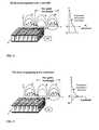
FIG. 8 illustrates an artificial magnetic conductor (AMC) 800. TheAMC 800 includes anarray 802 that is in one embodiment a coplanar array of resonantloops or artificialmagnetic molecules 804 which are strongly capacitively coupledto each other, forming a capacitive frequency selective surface (FSS). Theresonant loops 804 in the illustrated embodiment are uniformly spaced and at aheighth above a solidconductive ground plane 806. An array of electrically short,conductive posts orvias 808 are attached to theground plane 806 only and have alengthh. Eachloop 804 includes a lumpedcapacitive load 810. The one or morelayers of artificial magnetic molecules (AMMs) or resonant loops of the artificialmagnetic conductor 800 create a frequency dependent permeability in thezdirection, normal to the surface of theAMC 800.
AnAMC 800 with a single layer of artificialmagnetic molecules 804 isshown in FIG. 8. In this embodiment, each loop and capacitor load aresubstantially identical so that all loops have substantially the same resonantfrequency. In alternative embodiments, loops having different characteristics maybe used. In physical realizations, due to manufacturing tolerances and othercauses, individual loops and their associated resonant frequencies will notnecessarily be identical.
AnAMC 900 with multiple layers of artificialmagnetic molecules 804 isshown in FIG. 9. FIG. 10 is a cross sectional view of the artificialmagneticconductor 900 of FIG. 9. TheAMC 900 includes afirst layer 902 ofloops 804resonant at a first frequency f1. TheAMC 900 includes asecond layer 904 ofloops 804 resonant at a second frequency f2. Eachloop 804 of thefirst layer 902of loops includes a lumpedcapacitive load C 1 908. Eachloop 804 of thesecondlayer 904 of loops includes a lumpedcapacitive load C 2 906. The lumped capacitances may be the same but need not be. In combination, thefirst layer 902ofloops 804 and thesecond layer 906 ofloops 904 form a frequency selectivesurface (FSS)layer 910 disposed on aspacer layer 912. In practical application,the low frequency limit of the transverse effective relative permittivity, ε1x and ε1y,for themultiple layer AMC 900 lies between 100 and 2000. Accordingly, strongcapacitive coupling is present betweenloops
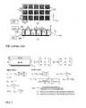
FIG. 11 illustrates a first physical embodiment of aloop 1100 for use in anartificial magnetic conductor such as theAMC 800 of FIG. 8. Conducting loopssuch asloop 1100 which form the artificial magnetic molecules can beimplemented in a variety of shapes such as square, rectangular, circular, triangular,hexagonal, etc. In the embodiment of FIG. 11, theloop 1100 is square in shape.Notches 1102 can be designed in the loops to increase the self inductance, whichlowers the resonant frequency of the AMMs.Notches 1102 andgaps 1104 canalso be introduced to engineer the performance of theloop 1100 to a particulardesired response. For example, the bands or resonance frequencies may be chosenby selecting a particular shape for theloop 1100. In general, agap 1104 cuts allthe way through a side of theloop 1100 from the center of theloop 1100 to theperiphery. In contrast, a notch cuts through only a portion of a side between thecenter and periphery of theloop 1100. FIG. 11 illustrates a selection of potentialsquare loop designs.
FIG. 12 illustrates a portion of a two layer artificial magnetic conductorwhose FSS layer uses a square loop of FIG. 11(d). Wide loops with relativelylarge surface area promote capacitive coupling between loops of adjacent layerswhen used in a two-layer overlapping AMC, as illustrated in FIG. 12. Anoverlapregion 1202 at thegap 1104 provides the series capacitive coupling required forloop resonance.
In one preferred embodiment, loops of the type illustrated in FIGS. 11 and12 are formed on surfaces of dielectric materials using conventional printed circuit board (PCB) manufacturing techniques. For example, a metallic layer is depositedon a surface of the PCB and subsequently patterned by chemical etching or othertechnique. Such processes provide precise control of sizes, spacing anduniformity of printed features.
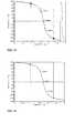
FIG. 13 and FIG. 14 show simulation results for the normal-incidencereflection phase of the AMC illustrated in FIG. 12. In both simulations, theincident electric field is y-polarized. In the simulation illustrated in FIG. 13,P=10.4mm, h=6mm, t=0.2mm, s=7.2mm, w=1.6mm, g2=0.4mm, εr1=εr2=3.38.FIG. 13 shows a fundamental resonance near 1.685 GHz, and a second resonancenear 2.8 GHz. In FIG. 14, when the gap in the loops is eliminated so that theloops are shorted and g2=0 in FIG. 12, then only one resonance is obtained. Thereason that theAMC 800 withgaps 1104 has a second resonance is that theeffective transverse permittivity of the frequency selective surface has becomefrequency dependent. A simple capacitive model is no longer adequate.
FIG. 15 shows equivalent circuits for portions of the artificialmagneticconductor 800 of FIG. 8. FIG. 15(a) illustrates the second Foster canonical formfor the input admittance of a one-port circuit, which is a general analytic model forthe effective transverse permittivity of complex frequency selective surface (FSS)structures. FIG. 15(b) gives an example of a specific equivalent circuit model foran FSS whereby two material or intrinsic resonances are assumed. FIG. 15(c)shows the TEM mode equivalent circuit for plane waves normally incident on atwo layer AMC, such asAMC 900 of FIG. 9. As noted above, the modelsdeveloped herein are useful for characterizing, understanding, designing andengineering devices such as the AMCs described and illustrated herein. Thesemodels represent approximations of actual device behavior.
Complex loop FSS structures, such as that shown in FIG. 12, have adispersive, or frequency dependent, effective transverse permittivity which can beproperly modeled using a more complex circuit model. Furthermore, analyticcircuit models for dispersive dielectric media can be extended in applicability tomodel the transverse permittivity of complex FSS structures. The second Foster canonical circuit for one-port networks, shown in FIG. 15(a), is a general casewhich should cover all electrically-thin FSS structures. Each branch manifests anintrinsic resonance of the FSS. For an FSS made from low loss materials, Rn isexpected to be very low, hence resonances are expected to be Lorentzian.
The effective sheet capacitance for the loop FSS shown in FIG. 12 has aLorentz resonance somewhere between 1.685 GHz and 2.8 GHz. In fact, if thetransverse permittivity of this FSS is modeled using only a three-branchadmittance circuit, as shown in FIG. 15(b), theε1y curve 1602 shown in the uppergraph of FIG. 16 is obtained. Two FSS material resonances are evident near 2.25GHz and 3.2 GHz. The ε1y curve 1604 is the transverse relative permittivityrequired to achieve resonance for the AMC, a zero degree reflection phase. Thiscurve 1604 is simply found by equating the capacitive reactance of the FSS,Xc = 1/(ωC) = 1/(ωε1yεot), to the inductive reactance of the spacer layer,XL = ωL = ωµ2xµoh, and solving for transverse relative permittivity:
ε1y = 1/(ω2µ2xµoεoht). Intersections of thecurve 1602 and thecurve 1604 definethe frequencies for reflection phase resonance. The reflection phase curve shownin the lower graph of FIG. 16 was computed using the transmission line modelshown in FIG. 15(c) in which the admittance of the FSS is placed in parallel withthe shorted transmission line of lengthh representing the spacer layer andbackplane. This circuit model predicts a dual resonance near 1.2 GHz and 2.75GHz, which are substantially the frequencies of intersection in theε1y plot. Thusthe multiple resonant branches in the analytic circuit model for the FSS transversepermittivity can be used to explain the existence of multiple AMC phaseresonances. Any realizable FSS structure can be modeled accurately using asufficient number of shunt branches.
ε1y = 1/(ω2µ2xµoεoht). Intersections of the
There are many additional square loop designs which may be implementedin FSS structures to yield a large transverse effective permittivity. More examplesare shown in FIGS. 17, 20 and 21 where loops of substantially identical size andsimilar shape are printed on opposite sides of a single dielectric layer FSS. Reflection phase results for x and y polarized electric fields applied to an AMC ofthe design shown in FIG. 17 are shown in FIGS. 18 and 19. In this design, P=400mils, g1=30 mils, g2=20 mils, r=40 mils, w=30 mils, t=8 mils, and h=60 mils.εr=3.38 in both FSS and spacer layers since this printed AMC is fabricated usingRogers R04003 substrate material. In the center of each loop, a via is fabricatedusing a 20 mil diameter plated through hole.
FIG. 18 shows measured reflection phase data for anx polarized electricfield normally incident on the AMC of FIG. 17. Resonant frequencies areobserved near 1.6 GHz and 3.45 GHz. Similarly, FIG. 19 shows measuredreflection phase data for a y polarized electric field normally incident on the AMCof FIG. 17. Resonant frequencies are observed near 1.4 GHz and 2.65 GHz.
In FIGS. 18 and 19, a dual resonant performance is clearly seen in thephase data. For the specific case fabricated, each polarization sees differentresonant frequencies. However, it is believed that the design has sufficientdegrees of freedom to make the resonance frequencies polarization independent.
FIG. 21 shows an additional alternative embodiment for a frequencyselective surface implemented with square loops. The illustrated loop design ofFIG. 21 has overlappingsquare loops 2100 on eachlayer deepnotches 2102 cut from thecenter 2104 toward each corner.Gaps
An alternative type of dispersive capacitive FSS structure can be createdwhereloops 2402 are printed on the one side and notchedpatches 2404 are printedon the other side of a single dielectric layer FSS. An example is shown in FIG. 24.
In addition to the square loops illustrated in FIGS. 17, 20, 21 and 24,hexagonal loops can be printed in a variety of shapes that include notches which increase the loop self inductance. These notches may vary in number andposition, and they are not necessarily the same size in a given loop. Furthermore,loops printed on opposite sides of a dielectric layer can have different sizes andfeatures. There are a tremendous number of independent variables which uniquelydefine a multilayer loop FSS structure.
Six possibilities of hexagonal loop FSS designs are illustrated in FIGS. 25,26 and 27. In each of FIGS. 25, 26 and 27, afirst layer 902 of loops iscapacitively coupled with a second layer ofloops 904. The hexagonal loopspresented here are intended to be regular hexagons. Distorted hexagons could beimagined in this application, but their advantage is unknown at this time.
FIG. 28 illustrates an effective media model for ahigh impedance surface 2800. The general effective media model of FIG. 28 is applicable to highimpedance surfaces such as the prior arthigh impedance surface 100 of FIG. 1 andthe artificial magnetic conductor (AMC) 800 of FIG. 8. TheAMC 800 includestwo distinct electrically-thin layers, a frequency selective surface (FSS) 802 and aspacer layer 804. Eachlayer layer AMC 800 of FIG. 8 but merely models the performance for engineering andanalysis. Changes may be made to aspects of the effective media model withoutaltering the overall effectiveness of the model or the benefits obtained therefrom.
As will be described, thehigh impedance surface 2800 for theAMC 800 ofFIG. 8 is characterized by an effective media model which includes an upper layerand a lower layer, each layer having a unique tensor permittivity and tensorpermeability. Each layer's tensor permittivity and each layer's tensor permeability have non-zero elements on the main tensor diagonal only, with the x and y tensordirections being in-plane with each respective layer and the z tensor directionbeing normal to each layer. The result for theAMC 800 is an AMC resonant atmultiple resonance frequencies.
In the two-layer effective media model of FIG. 28, eachlayer layer layer
Each of the twolayers high impedance surface 2800 has four material parameters: the transverseand normal permittivity, and the transverse and normal permeability. Given twolayers
| Wave Type | Electric Field Sees | Magnetic Field Sees |
| TEM, normal incidence | ε1t ,ε2t | µ1t , µ2t |
| TE to x | ε1t, ε2t | µ1t , µ2t, µ1n , µ2n |
| TM to x | ε1t , ε2t , ε1n, ε2n | µ1t , µ2t |
A transverse electric (TE) surface wave propagating on thehigh impedancesurface 2800 has a field structure shown in FIG. 4. By definition, the electric field(E field) is transverse to the direction of wave propagation, the +x direction. It isalso parallel to the surface. So the electric field sees only transverse permittivities.However, the magnetic field (H field) lines form loops in thexz plane whichencircle the E field lines. So the H field sees both transverse and normalpermeabilities.
The transverse magnetic (TM) surface wave has a field structure shown inFIG. 5. Note that, for TM waves, the role of the E and H fields is reversed relativeto the TE surface waves. For TM modes, the H field is transverse to the directionof propagation, and the E field lines (in thexz plane) encircle the H field. So theTM mode electric field sees both transverse and normal permittivities.
The following conclusions may be drawn from the general effective mediamodel of FIG. 28. First, ε1n andε2n are fundamental parameters which permitindependent control of the TM modes, and hence the dominant TM mode cutofffrequency. Second, µ1n and µ2n are fundamental parameters which permitindependent control of the TE modes, and hence the dominant TE mode cutofffrequency.
One way to distinguish between prior arthigh impedance surface 100 ofFIG. 1 and an AMC such as AMC 800 (FIG. 8) or AMC 900 (FIG. 9, FIG. 10) isby examining the differences in the elements of theµi andεi tensors. FIG. 29shows a prior arthigh impedance surface 100 whose frequencyselective surface 102 is a coplanar layer of square conductive patches of size b x b, separated by agap of dimension g.. In thehigh impedance surface 100, εD is the relativepermittivity of the background or host dielectric media in thespacer layer 104, µDis the relative permeability of this background media in thespacer layer 104, andα is the ratio of cross sectional area of each rod or post to the area A of the unitcell in the rodded media orspacer layer 104. The relative permittivityεavg = 1+εD / 2 is the average of the relative dielectric constants of air and the background media in thespacer layer 104.C denotes the fixed FSS sheetcapacitance.
The permittivity tensor for both the high-impedance surface 100 and theAMCs high impedance surface 100 has a squarelattice of both rods and square patches, each having the same period. Therefore,unit cell areaA = (g +b)2. Also, α= (πd2/4)/A, whered is the diameter of therods or posts. The dimensions of the rods or posts are very small relative to thewavelength at the resonance frequencies. The rods or posts may be realized byany suitable physical embodiment, such as plated-through holes or vias in aconventional printed circuit board or by wires inserted through a foam. Anytechnique for creating a forest of vertical conductors (i.e., parallel to the z axis),each conductor being electrically coupled with the ground plane, may be used.The conductors or rods may be circular in cross section or may be flat strips of anycross section whose dimensions are small with respect to the wavelength λ in thehost medium or dielectric of the spacer layer. In this context, small dimensions forthe rods are generally in the range of λ/1000 to λ/25.
In some embodiments, theAMC 800 has transverse permittivity in the ytensor direction substantially equal to the transverse permittivity in the x tensordirection. This yields an isotropic high impedance surface in which the impedancealong the y axis is substantially equal to the impedance along the x axis. Inalternative embodiments, the transverse permittivity in the y tensor direction doesnot equal the transverse permittivity in the x tensor direction to produce ananisotropic high impedance surface, meaning the impedances along the two inplaneaxes are not equal. Examples of the latter are shown in Figures 17 and 21.
Effective media models for substantially modelling both thehighimpedance surface 100 and anAMC AMC impedance surface 100. These are the transverse permittivity ε1x, ε1y andthe normal permeability µ1z, both of the upper layer or frequency selective surface. The model for the lower layer or spacer layer is the same in both thehighimpedance surface 100 and theAMC 

In Table 2,Y(ω) is an admittance function written in the second Fostercanonical form for a one port circuit:

This admittance functionY(ω) is related to the sheet capacitance(C = ε1tεot) of theFSS 802 of theAMC high impedance surface 100 has an FSS capacitance which is frequencyindependent. However, theAMC FSS 802 whose capacitancecontains inductive elements in such a way that the sheet capacitance undergoesone or more Lorentz resonances at prescribed frequencies. Such resonances areaccomplished by integrating into theFSS 802 the physical features of resonantloop structures, also referred to as artificial magnetic molecules. As the frequency of operation is increased, the capacitance of theFSS 802 will undergo a series ofabrupt changes in total capacitance.
FIG. 30 illustrates sheet capacitance for the frequencyselective surface 802of theAMC 800 of FIG. 8 and theAMC 900 of FIG. 9. FIG. 30(a) shows that thecapacitance of theFSS 802 is frequency dependent. FIG 30(b) shows a Debyeresponse obtained from a lossy FSS where Rn is significant. In FIG. 30, two FSSresonances (ωn =1/Ln Cn spacer layer 804, which is a constant, to achieve a resonance in the reflectioncoefficient phase for theAMC AMC
In contrast, the two-layerhigh impedance surface 100 will offer reflectionphase resonances at a fundamental frequency, plus higher frequencies near wherethe electrical thickness of the bottom layer isnπ and n is an integer. These higherfrequency resonances are approximately harmonically related, and henceuncontrollable.
A second difference in the tensor effective media properties for thehighimpedance surface 100 andAMC 800 is in the normal permeability componentµ1n. Thehigh impedance surface 100 has a constant µ1n, whereas theAMC 

This impedance function is sufficient to accurately describe the normalpermeability of theFSS 802 in anAMC
The prior art high-impedance surface 100, whoseFSS 102 is composed ofmetal patches, has a lower bound for µ1n. This lower bound is inversely related tothe transverse permittivity according to the approximate relation µ1n ≈ 2/ε1t.Regardless of the FSS sheet capacitance, µ1n is anchored at this value for the priorart high-impedance surface 100. However, a normal permeability which is lowerthan µ1n = 2/ε1t is needed to cut off the guided bound TE mode in all of the high-impedancebands of a multi-band AMC such asAMC 800 andAMC 900.
The overlapping loops used in theFSS 802 of theAMC AMC 800 andAMC 900. The illustrated embodiment uses arrays of overlapping loops as theFSS layer 802, or in conjunction with a capacitive FSS layer, tuned individually orin multiplicity with a capacitance. This capacitance may be the self capacitance ofthe loops, the capacitance offered by adjacent layers, or the capacitance of externalcapacitors attached to the FSS. such as chip capacitors. The loops and capacitanceare tuned so as to obtain a series of Lorentz resonances across the desired bands ofoperation. Just as in the case of the resonant FSS transverse permittivity, theresonances of the artificial magnetic molecules affords the designer a series ofstaircase steps of progressively dropping normal permeability. Again, the regionof rapidly changing normal permeability around the resonances may be used toadvantage in narrowband operations. However, the illustrated embodiment usesplateaus of extended depressed normal permeability to suppress the onset ofguided bound TE surface waves within the desired bands of high-impedanceoperation.
In summary, the purpose of the resonance in the effective transversepermittivities ε1t is to provide multiple bands of high surface impedance. The purpose of the resonances in the normal permeability µ1n is to depress its value soas to prevent the onset of TE modes inside the desired bands of high impedanceoperation.
In some applications, an artificial magnetic conductor having more thantwo layers of loops separated by more than a single dielectric layer may provideimportant performance advantages. FIG. 31 illustrates an artificialmagneticconductor 3100 including a multiple layer frequency selective surface (FSS) 3102.TheAMC 3100 further includes aconductive ground plane 3104 and a roddedmedia forming aspacer layer 3106 disposed between theFSS 3102 and theconductive ground plane 3104. TheFSS 3102 has a frequency dependentpermeability µ1z in a direction normal to the frequencydependent surface 3102.Exemplary dimensions and coordinate axes are shown in FIG. 31.
TheFSS 3102 includes three arrays of substantially coplanar artificialmagnetic molecules. The artificial magnetic molecules are preferablyimplemented as overlapping capacitively coupled loops. In the embodiment ofFIG. 31, theFSS 3102 includes afirst array 3112, asecond array 3114 and athirdarray 3116 of artificial magnetic molecules. Afirst dielectric layer 3118 separatesthefirst array 3112 of artificial magnetic molecules from thesecond array 3114 ofartificial magnetic molecules.
Thearrays
Also, theAMC 3100 includes threelayers dielectric layers
Thespacer layer 3106 includesmetallic rods 3108 periodically positionedin a dielectric material. Preferably, each loop of each array ofloops rod 3108 of thespacer layer 3106. Any suitablemanufacturing method, for example, as described above, may be used tomanufacture the rodded media of thespacer layer 3108.
FIG. 32 illustrates a top view of the multiple-layer frequencyselectivesurface 3102 of FIG. 31. FIG. 32 shows thefirst array 3112, thesecond array 3114 and thethird array 3116 of the frequencyselective surface 3102. A portiononly of each array is visible to illustrate the layering of the respective arrays.
In FIG. 32, each of thearrays FSS 3102. Each loop isnotched to tailor the self-inductance of the loop and includes a gap to tailor theresonant frequency of the loop. The embodiment of FIGS. 31 and 32 is illustrativeonly. In other embodiments, different size and shape loops may be used alongwith different numbers of layers or arrays.
From the foregoing, it can be seen that the present embodiments provide avariety of high-impedance surfaces or artificial magnetic conductors which exhibitmultiple reflection phase resonances, or multi-band performance. The resonantfrequencies for high surface impedance are not harmonically related, but occur atfrequencies which may be designed or engineered. This is accomplished bydesigning the tensor permittivity of the upper layer to have a behavior withfrequency which exhibits one or more Lorentzian resonances.
While a particular embodiment of the present invention has been shownand described, modifications may be made. Other methods of making or usinganisotropic materials with negative axial permittivity and depressed axialpermeability, for the purpose of constructing multiband surface wave suppressingAMCs, such as by using artificial dielectric and magnetic materials, are extensionsof the embodiments described herein. Any such method can be used to advantageby a person ordinarily skilled in the art by following the description herein for the interrelationship between the Lorentz material resonances and the positions of thedesired operating bands. Accordingly, it is therefore intended in the appendedclaims to cover such changes and modifications which follow in the true spirit andscope of the invention.
Claims (17)
- An antenna systemcharacterized by:an artificial magnetic conductor (AMC) (300) includinga frequency selective surface having a frequency dependentpermeability µ1z in a direction normal to the frequencydependent surface;a conductive ground plane (806) anda rodded media (808) disposed between the frequency selective surfaceand the conductive ground plane.
- The antenna system of claim 1 furthercharacterized by:an antenna (304) in proximity to the AMC.
- The antenna system of claim 2 wherein the frequency selective surfaceischaracterized by:a plurality of substantially identical periodically spaced loops (804)which are substantially coplanar and substantially uniformlyspaced a distanceh from the conductive ground plane.
- The antenna system of 3 wherein the loopscharacterized by a lowfrequency limit of transverse effective relative permittivity ε1x and ε1y in the plane ofthe frequency selective surface in the range 100 to 2000.
- The antenna system of claim 2 wherein the frequency selective surfaceischaracterized by a normal permeability µ1z which exhibits one or more Lorentzmaterial resonances at particular frequencies.
- The antenna system of claim 1 wherein the AMC is characterized to beresonant with a substantially zero degree reflection phase over two or more AMCresonant frequency bands and wherein the rodded media comprises a spacer layerincluding an array of metal posts extending through the spacer layer and wherein the afrequency selective surface (FSS) is disposed on the spacer layer, the frequencyselective surface, as an effective media, having one or more Lorentz resonances atpredetermined frequencies different from the two or more AMC resonant frequencybands.
- An antenna systemcharacterized by:an artificial magnetic conductor (300) includinga conductive ground plane (806),a spacer layer (808) disposed on the ground plane, andone or more arrays of coplanar loops (804) resonant at two or morefrequency bands, each loop having a similar shape and similarsize, the one or more arrays of coplanar loops producing afrequency dependent normal permeability µz; andan antenna (304) proximate the artificial magnetic conductor.
- The antenna system of claim 7 wherein the one or more arrays ofcoplanar loops arecharacterized by:a first array (902) of loops regularly spaced a with a period P in a first plane;
anda second array (904) of loops regularly spaced in a second plane. - The antenna system of claim 7 furthercharacterized by externalcapacitors to produce a series capacitance between adjacent loops.
- The antenna system of claim 7 furthercharacterized by one or moredielectric layers separating each of the one or more arrays of coplanar loops.
- An antenna systemcharacterized by:a conductive ground plane (806);a dielectric layer (912) perforated by conductive rods (808) in electricalcontact with the conductive ground plane;a frequency selective surface (910) disposed on the dielectric layer andincludinga first layer (902) of capacitively coupled loops resonant at a firstfrequency,a dielectric spacer layer, anda second layer (904) of capacitively coupled loops resonant at a secondfrequency, the frequency selective surface having a frequencydependent permeability in a direction substantially normal to thefrequency selectively surface; andan antenna (304) positioned proximate the frequency selective surface.
- An artificial magnetic conductor (300) resonant with a substantiallyzero degree reflection phase over at least two resonant frequency bands, the artificialmagnetic conductorcharacterized by a frequency selective surface having a pluralityof Lorentz resonances in transverse permittivity at independent, non-harmonicallyrelated, predetermined frequencies different from the resonant frequency bands.
- An artificial magnetic conductor (AMC) (300) resonant at multipleresonance frequencies, the AMCcharacterized by an effective media model, theeffective media modelcharacterized by:a first layer and a second layer, each layer having a layer tensor permittivityand a layer tensor permeability, each layer tensor permittivity and eachlayer tensor permeability having non-zero elements on a main diagonalonly, x and y tensor directions being in-plane with each respective layerand z tensor direction being normal to each layer.
- The AMC of claim 13 wherein the effective media model is furthercharacterized by:a first layercharacterized by transverse permittivities in the y tensor directionand the x tensor direction which are variable with frequency and whichexhibit one or more Lorentz resonances.
- The AMC of claim 14 wherein the transverse permittivity of the firstlayer is modeled by ε1t =Y(ω) /jωεot whereY(ω) is an admittance function described byFoster's second canonical form for a one port circuit,wherej is the imaginary operator, ω is radian frequency,εo is the permittivity of freespace,C∞ is the asymptotic limit on transverse capacitance of the first layer asω approaches an infinite value,Lo is the asymptotic limit on shunt inductance of themodel as ω approaches 0,Rn is a branch resistance,Ln is a branch inductance andCn is a branch capacitance.

- An artificial magnetic conductor (300) operable over at least a firsthigh-impedance frequency band and a second high-impedance frequency band as ahigh- impedance surface, the artificial magnetic conductor being defined by aneffective media modelcharacterized by:a spacer layer; anda frequency selective surface (FSS) disposed adjacent the spacer layer andhaving a transverse permittivity ε1t defined by ε1x = ε1y =Y(ω) /jωε0t,whereinY(ω) is a frequency dependent admittance function for thefrequency selective surface,j is the imaginary operator, ω corresponds to angular frequency, ε0 is the permittivity of free space, and tcorresponds to thickness of the frequency selective surface.
- The artificial magnetic conductor of claim 16 wherein the FSS layerhas a normal permeability µ1z defined by µ1z =Z(ω) /jωµ0t, wherein Z(ω) is a frequencydependent impedance function,j is the imaginary operator, ω corresponds to angularfrequency, µ0 is the permeability of free space, andt corresponds to thickness of thefrequency selective surface.

Applications Claiming Priority (4)
| Application Number | Priority Date | Filing Date | Title |
|---|---|---|---|
| US09/678,128US6512494B1 (en) | 2000-10-04 | 2000-10-04 | Multi-resonant, high-impedance electromagnetic surfaces |
| US678128 | 2000-10-04 | ||
| US704510 | 2000-11-01 | ||
| US09/704,510US6670932B1 (en) | 2000-11-01 | 2000-11-01 | Multi-resonant, high-impedance surfaces containing loaded-loop frequency selective surfaces |
Publications (2)
| Publication Number | Publication Date |
|---|---|
| EP1195847A2true EP1195847A2 (en) | 2002-04-10 |
| EP1195847A3 EP1195847A3 (en) | 2002-05-15 |
Family
ID=27101962
Family Applications (1)
| Application Number | Title | Priority Date | Filing Date |
|---|---|---|---|
| EP01308496AWithdrawnEP1195847A3 (en) | 2000-10-04 | 2001-10-04 | Multi-resonant, high-impedance surfaces containing loaded-loop frequency selective surfaces |
Country Status (4)
| Country | Link |
|---|---|
| EP (1) | EP1195847A3 (en) |
| JP (1) | JP2002204123A (en) |
| KR (1) | KR20020027225A (en) |
| AU (1) | AU762267B2 (en) |
Cited By (172)
| Publication number | Priority date | Publication date | Assignee | Title |
|---|---|---|---|---|
| WO2004025783A1 (en)* | 2002-09-14 | 2004-03-25 | Bae Systems Plc | Periodic electromagnetic structure |
| FR2859309A1 (en)* | 2003-09-02 | 2005-03-04 | Commissariat Energie Atomique | HIGH IMPEDANCE SUBSTRATE |
| US7315289B2 (en) | 2002-09-10 | 2008-01-01 | Fractus, S.A. | Coupled multiband antennas |
| EP1722618A4 (en)* | 2004-03-01 | 2008-10-29 | Nitta Corp | Electromagnetic wave absorber |
| US7486242B2 (en) | 2002-06-25 | 2009-02-03 | Fractus, S.A. | Multiband antenna for handheld terminal |
| CN103326107A (en)* | 2012-03-22 | 2013-09-25 | 美国博通公司 | Programmable antenna having a programmable substrate |
| US8842055B2 (en) | 2011-05-26 | 2014-09-23 | Texas Instruments Incorporated | High impedance surface |
| WO2015184867A1 (en)* | 2014-09-15 | 2015-12-10 | 中兴通讯股份有限公司 | Specular reflector and wireless terminal antenna device |
| US9544006B2 (en) | 2014-11-20 | 2017-01-10 | At&T Intellectual Property I, L.P. | Transmission device with mode division multiplexing and methods for use therewith |
| US9577306B2 (en) | 2014-10-21 | 2017-02-21 | At&T Intellectual Property I, L.P. | Guided-wave transmission device and methods for use therewith |
| US9596001B2 (en) | 2014-10-21 | 2017-03-14 | At&T Intellectual Property I, L.P. | Apparatus for providing communication services and methods thereof |
| US9608692B2 (en) | 2015-06-11 | 2017-03-28 | At&T Intellectual Property I, L.P. | Repeater and methods for use therewith |
| US9608740B2 (en) | 2015-07-15 | 2017-03-28 | At&T Intellectual Property I, L.P. | Method and apparatus for launching a wave mode that mitigates interference |
| US9615269B2 (en) | 2014-10-02 | 2017-04-04 | At&T Intellectual Property I, L.P. | Method and apparatus that provides fault tolerance in a communication network |
| US9627768B2 (en) | 2014-10-21 | 2017-04-18 | At&T Intellectual Property I, L.P. | Guided-wave transmission device with non-fundamental mode propagation and methods for use therewith |
| US9628116B2 (en) | 2015-07-14 | 2017-04-18 | At&T Intellectual Property I, L.P. | Apparatus and methods for transmitting wireless signals |
| US9640850B2 (en) | 2015-06-25 | 2017-05-02 | At&T Intellectual Property I, L.P. | Methods and apparatus for inducing a non-fundamental wave mode on a transmission medium |
| US9653770B2 (en) | 2014-10-21 | 2017-05-16 | At&T Intellectual Property I, L.P. | Guided wave coupler, coupling module and methods for use therewith |
| US9654173B2 (en) | 2014-11-20 | 2017-05-16 | At&T Intellectual Property I, L.P. | Apparatus for powering a communication device and methods thereof |
| US9661505B2 (en) | 2013-11-06 | 2017-05-23 | At&T Intellectual Property I, L.P. | Surface-wave communications and methods thereof |
| US9667317B2 (en) | 2015-06-15 | 2017-05-30 | At&T Intellectual Property I, L.P. | Method and apparatus for providing security using network traffic adjustments |
| US9685992B2 (en) | 2014-10-03 | 2017-06-20 | At&T Intellectual Property I, L.P. | Circuit panel network and methods thereof |
| US9692101B2 (en) | 2014-08-26 | 2017-06-27 | At&T Intellectual Property I, L.P. | Guided wave couplers for coupling electromagnetic waves between a waveguide surface and a surface of a wire |
| US9699785B2 (en) | 2012-12-05 | 2017-07-04 | At&T Intellectual Property I, L.P. | Backhaul link for distributed antenna system |
| US9705610B2 (en) | 2014-10-21 | 2017-07-11 | At&T Intellectual Property I, L.P. | Transmission device with impairment compensation and methods for use therewith |
| US9705561B2 (en) | 2015-04-24 | 2017-07-11 | At&T Intellectual Property I, L.P. | Directional coupling device and methods for use therewith |
| US9712350B2 (en) | 2014-11-20 | 2017-07-18 | At&T Intellectual Property I, L.P. | Transmission device with channel equalization and control and methods for use therewith |
| US9722318B2 (en) | 2015-07-14 | 2017-08-01 | At&T Intellectual Property I, L.P. | Method and apparatus for coupling an antenna to a device |
| US9729197B2 (en) | 2015-10-01 | 2017-08-08 | At&T Intellectual Property I, L.P. | Method and apparatus for communicating network management traffic over a network |
| US9735833B2 (en) | 2015-07-31 | 2017-08-15 | At&T Intellectual Property I, L.P. | Method and apparatus for communications management in a neighborhood network |
| US9742462B2 (en) | 2014-12-04 | 2017-08-22 | At&T Intellectual Property I, L.P. | Transmission medium and communication interfaces and methods for use therewith |
| US9748626B2 (en) | 2015-05-14 | 2017-08-29 | At&T Intellectual Property I, L.P. | Plurality of cables having different cross-sectional shapes which are bundled together to form a transmission medium |
| US9749013B2 (en) | 2015-03-17 | 2017-08-29 | At&T Intellectual Property I, L.P. | Method and apparatus for reducing attenuation of electromagnetic waves guided by a transmission medium |
| US9749053B2 (en) | 2015-07-23 | 2017-08-29 | At&T Intellectual Property I, L.P. | Node device, repeater and methods for use therewith |
| US9762289B2 (en) | 2014-10-14 | 2017-09-12 | At&T Intellectual Property I, L.P. | Method and apparatus for transmitting or receiving signals in a transportation system |
| US9769020B2 (en) | 2014-10-21 | 2017-09-19 | At&T Intellectual Property I, L.P. | Method and apparatus for responding to events affecting communications in a communication network |
| US9769128B2 (en) | 2015-09-28 | 2017-09-19 | At&T Intellectual Property I, L.P. | Method and apparatus for encryption of communications over a network |
| US9768833B2 (en) | 2014-09-15 | 2017-09-19 | At&T Intellectual Property I, L.P. | Method and apparatus for sensing a condition in a transmission medium of electromagnetic waves |
| US9780834B2 (en) | 2014-10-21 | 2017-10-03 | At&T Intellectual Property I, L.P. | Method and apparatus for transmitting electromagnetic waves |
| US9787412B2 (en) | 2015-06-25 | 2017-10-10 | At&T Intellectual Property I, L.P. | Methods and apparatus for inducing a fundamental wave mode on a transmission medium |
| US9793954B2 (en) | 2015-04-28 | 2017-10-17 | At&T Intellectual Property I, L.P. | Magnetic coupling device and methods for use therewith |
| US9794003B2 (en) | 2013-12-10 | 2017-10-17 | At&T Intellectual Property I, L.P. | Quasi-optical coupler |
| US9793955B2 (en) | 2015-04-24 | 2017-10-17 | At&T Intellectual Property I, Lp | Passive electrical coupling device and methods for use therewith |
| US9793951B2 (en) | 2015-07-15 | 2017-10-17 | At&T Intellectual Property I, L.P. | Method and apparatus for launching a wave mode that mitigates interference |
| US9800327B2 (en) | 2014-11-20 | 2017-10-24 | At&T Intellectual Property I, L.P. | Apparatus for controlling operations of a communication device and methods thereof |
| US9820146B2 (en) | 2015-06-12 | 2017-11-14 | At&T Intellectual Property I, L.P. | Method and apparatus for authentication and identity management of communicating devices |
| US9838078B2 (en) | 2015-07-31 | 2017-12-05 | At&T Intellectual Property I, L.P. | Method and apparatus for exchanging communication signals |
| US9838896B1 (en) | 2016-12-09 | 2017-12-05 | At&T Intellectual Property I, L.P. | Method and apparatus for assessing network coverage |
| US9836957B2 (en) | 2015-07-14 | 2017-12-05 | At&T Intellectual Property I, L.P. | Method and apparatus for communicating with premises equipment |
| US9847566B2 (en) | 2015-07-14 | 2017-12-19 | At&T Intellectual Property I, L.P. | Method and apparatus for adjusting a field of a signal to mitigate interference |
| US9847850B2 (en) | 2014-10-14 | 2017-12-19 | At&T Intellectual Property I, L.P. | Method and apparatus for adjusting a mode of communication in a communication network |
| US9853342B2 (en) | 2015-07-14 | 2017-12-26 | At&T Intellectual Property I, L.P. | Dielectric transmission medium connector and methods for use therewith |
| US9860075B1 (en) | 2016-08-26 | 2018-01-02 | At&T Intellectual Property I, L.P. | Method and communication node for broadband distribution |
| US9866309B2 (en) | 2015-06-03 | 2018-01-09 | At&T Intellectual Property I, Lp | Host node device and methods for use therewith |
| US9866276B2 (en) | 2014-10-10 | 2018-01-09 | At&T Intellectual Property I, L.P. | Method and apparatus for arranging communication sessions in a communication system |
| US9865911B2 (en) | 2015-06-25 | 2018-01-09 | At&T Intellectual Property I, L.P. | Waveguide system for slot radiating first electromagnetic waves that are combined into a non-fundamental wave mode second electromagnetic wave on a transmission medium |
| US9871283B2 (en) | 2015-07-23 | 2018-01-16 | At&T Intellectual Property I, Lp | Transmission medium having a dielectric core comprised of plural members connected by a ball and socket configuration |
| US9871282B2 (en) | 2015-05-14 | 2018-01-16 | At&T Intellectual Property I, L.P. | At least one transmission medium having a dielectric surface that is covered at least in part by a second dielectric |
| US9876571B2 (en) | 2015-02-20 | 2018-01-23 | At&T Intellectual Property I, Lp | Guided-wave transmission device with non-fundamental mode propagation and methods for use therewith |
| US9876605B1 (en) | 2016-10-21 | 2018-01-23 | At&T Intellectual Property I, L.P. | Launcher and coupling system to support desired guided wave mode |
| US9876264B2 (en) | 2015-10-02 | 2018-01-23 | At&T Intellectual Property I, Lp | Communication system, guided wave switch and methods for use therewith |
| US9882257B2 (en) | 2015-07-14 | 2018-01-30 | At&T Intellectual Property I, L.P. | Method and apparatus for launching a wave mode that mitigates interference |
| US9882277B2 (en) | 2015-10-02 | 2018-01-30 | At&T Intellectual Property I, Lp | Communication device and antenna assembly with actuated gimbal mount |
| US9887447B2 (en) | 2015-05-14 | 2018-02-06 | At&T Intellectual Property I, L.P. | Transmission medium having multiple cores and methods for use therewith |
| US9893795B1 (en) | 2016-12-07 | 2018-02-13 | At&T Intellectual Property I, Lp | Method and repeater for broadband distribution |
| CN107706528A (en)* | 2016-08-08 | 2018-02-16 | 华为技术有限公司 | Antenna system |
| US9904535B2 (en) | 2015-09-14 | 2018-02-27 | At&T Intellectual Property I, L.P. | Method and apparatus for distributing software |
| US9906269B2 (en) | 2014-09-17 | 2018-02-27 | At&T Intellectual Property I, L.P. | Monitoring and mitigating conditions in a communication network |
| US9912419B1 (en) | 2016-08-24 | 2018-03-06 | At&T Intellectual Property I, L.P. | Method and apparatus for managing a fault in a distributed antenna system |
| US9912381B2 (en) | 2015-06-03 | 2018-03-06 | At&T Intellectual Property I, Lp | Network termination and methods for use therewith |
| US9912027B2 (en) | 2015-07-23 | 2018-03-06 | At&T Intellectual Property I, L.P. | Method and apparatus for exchanging communication signals |
| US9913139B2 (en) | 2015-06-09 | 2018-03-06 | At&T Intellectual Property I, L.P. | Signal fingerprinting for authentication of communicating devices |
| US9911020B1 (en) | 2016-12-08 | 2018-03-06 | At&T Intellectual Property I, L.P. | Method and apparatus for tracking via a radio frequency identification device |
| US9917341B2 (en) | 2015-05-27 | 2018-03-13 | At&T Intellectual Property I, L.P. | Apparatus and method for launching electromagnetic waves and for modifying radial dimensions of the propagating electromagnetic waves |
| US9930668B2 (en) | 2013-05-31 | 2018-03-27 | At&T Intellectual Property I, L.P. | Remote distributed antenna system |
| US9927517B1 (en) | 2016-12-06 | 2018-03-27 | At&T Intellectual Property I, L.P. | Apparatus and methods for sensing rainfall |
| US9948333B2 (en) | 2015-07-23 | 2018-04-17 | At&T Intellectual Property I, L.P. | Method and apparatus for wireless communications to mitigate interference |
| US9948354B2 (en) | 2015-04-28 | 2018-04-17 | At&T Intellectual Property I, L.P. | Magnetic coupling device with reflective plate and methods for use therewith |
| US9954287B2 (en) | 2014-11-20 | 2018-04-24 | At&T Intellectual Property I, L.P. | Apparatus for converting wireless signals and electromagnetic waves and methods thereof |
| US9967173B2 (en) | 2015-07-31 | 2018-05-08 | At&T Intellectual Property I, L.P. | Method and apparatus for authentication and identity management of communicating devices |
| US9973940B1 (en) | 2017-02-27 | 2018-05-15 | At&T Intellectual Property I, L.P. | Apparatus and methods for dynamic impedance matching of a guided wave launcher |
| US9991580B2 (en) | 2016-10-21 | 2018-06-05 | At&T Intellectual Property I, L.P. | Launcher and coupling system for guided wave mode cancellation |
| US9998870B1 (en) | 2016-12-08 | 2018-06-12 | At&T Intellectual Property I, L.P. | Method and apparatus for proximity sensing |
| US9999038B2 (en) | 2013-05-31 | 2018-06-12 | At&T Intellectual Property I, L.P. | Remote distributed antenna system |
| US9997819B2 (en) | 2015-06-09 | 2018-06-12 | At&T Intellectual Property I, L.P. | Transmission medium and method for facilitating propagation of electromagnetic waves via a core |
| US10009065B2 (en) | 2012-12-05 | 2018-06-26 | At&T Intellectual Property I, L.P. | Backhaul link for distributed antenna system |
| US10009901B2 (en) | 2015-09-16 | 2018-06-26 | At&T Intellectual Property I, L.P. | Method, apparatus, and computer-readable storage medium for managing utilization of wireless resources between base stations |
| US10009063B2 (en) | 2015-09-16 | 2018-06-26 | At&T Intellectual Property I, L.P. | Method and apparatus for use with a radio distributed antenna system having an out-of-band reference signal |
| US10009067B2 (en) | 2014-12-04 | 2018-06-26 | At&T Intellectual Property I, L.P. | Method and apparatus for configuring a communication interface |
| US10020587B2 (en) | 2015-07-31 | 2018-07-10 | At&T Intellectual Property I, L.P. | Radial antenna and methods for use therewith |
| US10020844B2 (en) | 2016-12-06 | 2018-07-10 | T&T Intellectual Property I, L.P. | Method and apparatus for broadcast communication via guided waves |
| US10027397B2 (en) | 2016-12-07 | 2018-07-17 | At&T Intellectual Property I, L.P. | Distributed antenna system and methods for use therewith |
| US10033108B2 (en) | 2015-07-14 | 2018-07-24 | At&T Intellectual Property I, L.P. | Apparatus and methods for generating an electromagnetic wave having a wave mode that mitigates interference |
| US10033107B2 (en) | 2015-07-14 | 2018-07-24 | At&T Intellectual Property I, L.P. | Method and apparatus for coupling an antenna to a device |
| US10044409B2 (en) | 2015-07-14 | 2018-08-07 | At&T Intellectual Property I, L.P. | Transmission medium and methods for use therewith |
| CN108470973A (en)* | 2018-03-09 | 2018-08-31 | 南京航空航天大学 | Broadband RCS based on gap load reduces super surface |
| US10069535B2 (en) | 2016-12-08 | 2018-09-04 | At&T Intellectual Property I, L.P. | Apparatus and methods for launching electromagnetic waves having a certain electric field structure |
| US10079661B2 (en) | 2015-09-16 | 2018-09-18 | At&T Intellectual Property I, L.P. | Method and apparatus for use with a radio distributed antenna system having a clock reference |
| US10090594B2 (en) | 2016-11-23 | 2018-10-02 | At&T Intellectual Property I, L.P. | Antenna system having structural configurations for assembly |
| US10090606B2 (en) | 2015-07-15 | 2018-10-02 | At&T Intellectual Property I, L.P. | Antenna system with dielectric array and methods for use therewith |
| US10103801B2 (en) | 2015-06-03 | 2018-10-16 | At&T Intellectual Property I, L.P. | Host node device and methods for use therewith |
| US10103422B2 (en) | 2016-12-08 | 2018-10-16 | At&T Intellectual Property I, L.P. | Method and apparatus for mounting network devices |
| US10135147B2 (en) | 2016-10-18 | 2018-11-20 | At&T Intellectual Property I, L.P. | Apparatus and methods for launching guided waves via an antenna |
| US10135146B2 (en) | 2016-10-18 | 2018-11-20 | At&T Intellectual Property I, L.P. | Apparatus and methods for launching guided waves via circuits |
| US10135145B2 (en) | 2016-12-06 | 2018-11-20 | At&T Intellectual Property I, L.P. | Apparatus and methods for generating an electromagnetic wave along a transmission medium |
| US10136434B2 (en) | 2015-09-16 | 2018-11-20 | At&T Intellectual Property I, L.P. | Method and apparatus for use with a radio distributed antenna system having an ultra-wideband control channel |
| WO2018209422A1 (en)* | 2017-05-15 | 2018-11-22 | Valorbec Societe En Commandite | Contactless air-filled substrate integrated waveguide devices and methods |
| US10139820B2 (en) | 2016-12-07 | 2018-11-27 | At&T Intellectual Property I, L.P. | Method and apparatus for deploying equipment of a communication system |
| US10142086B2 (en) | 2015-06-11 | 2018-11-27 | At&T Intellectual Property I, L.P. | Repeater and methods for use therewith |
| US10144036B2 (en) | 2015-01-30 | 2018-12-04 | At&T Intellectual Property I, L.P. | Method and apparatus for mitigating interference affecting a propagation of electromagnetic waves guided by a transmission medium |
| US10148016B2 (en) | 2015-07-14 | 2018-12-04 | At&T Intellectual Property I, L.P. | Apparatus and methods for communicating utilizing an antenna array |
| US10170840B2 (en) | 2015-07-14 | 2019-01-01 | At&T Intellectual Property I, L.P. | Apparatus and methods for sending or receiving electromagnetic signals |
| US10168695B2 (en) | 2016-12-07 | 2019-01-01 | At&T Intellectual Property I, L.P. | Method and apparatus for controlling an unmanned aircraft |
| US10178445B2 (en) | 2016-11-23 | 2019-01-08 | At&T Intellectual Property I, L.P. | Methods, devices, and systems for load balancing between a plurality of waveguides |
| US10205655B2 (en) | 2015-07-14 | 2019-02-12 | At&T Intellectual Property I, L.P. | Apparatus and methods for communicating utilizing an antenna array and multiple communication paths |
| US10225025B2 (en) | 2016-11-03 | 2019-03-05 | At&T Intellectual Property I, L.P. | Method and apparatus for detecting a fault in a communication system |
| US10224634B2 (en) | 2016-11-03 | 2019-03-05 | At&T Intellectual Property I, L.P. | Methods and apparatus for adjusting an operational characteristic of an antenna |
| US10243270B2 (en) | 2016-12-07 | 2019-03-26 | At&T Intellectual Property I, L.P. | Beam adaptive multi-feed dielectric antenna system and methods for use therewith |
| US10264586B2 (en) | 2016-12-09 | 2019-04-16 | At&T Mobility Ii Llc | Cloud-based packet controller and methods for use therewith |
| US10291334B2 (en) | 2016-11-03 | 2019-05-14 | At&T Intellectual Property I, L.P. | System for detecting a fault in a communication system |
| US10291311B2 (en) | 2016-09-09 | 2019-05-14 | At&T Intellectual Property I, L.P. | Method and apparatus for mitigating a fault in a distributed antenna system |
| US10298293B2 (en) | 2017-03-13 | 2019-05-21 | At&T Intellectual Property I, L.P. | Apparatus of communication utilizing wireless network devices |
| US10305190B2 (en) | 2016-12-01 | 2019-05-28 | At&T Intellectual Property I, L.P. | Reflecting dielectric antenna system and methods for use therewith |
| US10312567B2 (en) | 2016-10-26 | 2019-06-04 | At&T Intellectual Property I, L.P. | Launcher with planar strip antenna and methods for use therewith |
| US10320586B2 (en) | 2015-07-14 | 2019-06-11 | At&T Intellectual Property I, L.P. | Apparatus and methods for generating non-interfering electromagnetic waves on an insulated transmission medium |
| US10326689B2 (en) | 2016-12-08 | 2019-06-18 | At&T Intellectual Property I, L.P. | Method and system for providing alternative communication paths |
| US10326494B2 (en) | 2016-12-06 | 2019-06-18 | At&T Intellectual Property I, L.P. | Apparatus for measurement de-embedding and methods for use therewith |
| US10341142B2 (en) | 2015-07-14 | 2019-07-02 | At&T Intellectual Property I, L.P. | Apparatus and methods for generating non-interfering electromagnetic waves on an uninsulated conductor |
| US10340601B2 (en) | 2016-11-23 | 2019-07-02 | At&T Intellectual Property I, L.P. | Multi-antenna system and methods for use therewith |
| US10340600B2 (en) | 2016-10-18 | 2019-07-02 | At&T Intellectual Property I, L.P. | Apparatus and methods for launching guided waves via plural waveguide systems |
| US10340983B2 (en) | 2016-12-09 | 2019-07-02 | At&T Intellectual Property I, L.P. | Method and apparatus for surveying remote sites via guided wave communications |
| US10340573B2 (en) | 2016-10-26 | 2019-07-02 | At&T Intellectual Property I, L.P. | Launcher with cylindrical coupling device and methods for use therewith |
| US10340603B2 (en) | 2016-11-23 | 2019-07-02 | At&T Intellectual Property I, L.P. | Antenna system having shielded structural configurations for assembly |
| US10355367B2 (en) | 2015-10-16 | 2019-07-16 | At&T Intellectual Property I, L.P. | Antenna structure for exchanging wireless signals |
| US10361489B2 (en) | 2016-12-01 | 2019-07-23 | At&T Intellectual Property I, L.P. | Dielectric dish antenna system and methods for use therewith |
| US10359749B2 (en) | 2016-12-07 | 2019-07-23 | At&T Intellectual Property I, L.P. | Method and apparatus for utilities management via guided wave communication |
| US10374316B2 (en) | 2016-10-21 | 2019-08-06 | At&T Intellectual Property I, L.P. | System and dielectric antenna with non-uniform dielectric |
| US10382976B2 (en) | 2016-12-06 | 2019-08-13 | At&T Intellectual Property I, L.P. | Method and apparatus for managing wireless communications based on communication paths and network device positions |
| US10389037B2 (en) | 2016-12-08 | 2019-08-20 | At&T Intellectual Property I, L.P. | Apparatus and methods for selecting sections of an antenna array and use therewith |
| US10389029B2 (en) | 2016-12-07 | 2019-08-20 | At&T Intellectual Property I, L.P. | Multi-feed dielectric antenna system with core selection and methods for use therewith |
| US10411356B2 (en) | 2016-12-08 | 2019-09-10 | At&T Intellectual Property I, L.P. | Apparatus and methods for selectively targeting communication devices with an antenna array |
| US10439675B2 (en) | 2016-12-06 | 2019-10-08 | At&T Intellectual Property I, L.P. | Method and apparatus for repeating guided wave communication signals |
| US10446936B2 (en) | 2016-12-07 | 2019-10-15 | At&T Intellectual Property I, L.P. | Multi-feed dielectric antenna system and methods for use therewith |
| CN110474163A (en)* | 2019-07-24 | 2019-11-19 | 西北工业大学 | A kind of frequency agility cavity antenna |
| US10498044B2 (en) | 2016-11-03 | 2019-12-03 | At&T Intellectual Property I, L.P. | Apparatus for configuring a surface of an antenna |
| US10530505B2 (en) | 2016-12-08 | 2020-01-07 | At&T Intellectual Property I, L.P. | Apparatus and methods for launching electromagnetic waves along a transmission medium |
| US10535928B2 (en) | 2016-11-23 | 2020-01-14 | At&T Intellectual Property I, L.P. | Antenna system and methods for use therewith |
| US10547348B2 (en) | 2016-12-07 | 2020-01-28 | At&T Intellectual Property I, L.P. | Method and apparatus for switching transmission mediums in a communication system |
| CN110858271A (en)* | 2018-08-26 | 2020-03-03 | 吴成彬 | Electronic passive tag identification system and method based on frequency selection characteristic |
| US10601494B2 (en) | 2016-12-08 | 2020-03-24 | At&T Intellectual Property I, L.P. | Dual-band communication device and method for use therewith |
| US10637149B2 (en) | 2016-12-06 | 2020-04-28 | At&T Intellectual Property I, L.P. | Injection molded dielectric antenna and methods for use therewith |
| US10650940B2 (en) | 2015-05-15 | 2020-05-12 | At&T Intellectual Property I, L.P. | Transmission medium having a conductive material and methods for use therewith |
| US10665942B2 (en) | 2015-10-16 | 2020-05-26 | At&T Intellectual Property I, L.P. | Method and apparatus for adjusting wireless communications |
| US10694379B2 (en) | 2016-12-06 | 2020-06-23 | At&T Intellectual Property I, L.P. | Waveguide system with device-based authentication and methods for use therewith |
| WO2020124251A1 (en)* | 2018-12-19 | 2020-06-25 | Huawei Technologies Canada Co., Ltd. | Dual end-fed broadside leaky-wave antenna |
| US10727599B2 (en) | 2016-12-06 | 2020-07-28 | At&T Intellectual Property I, L.P. | Launcher with slot antenna and methods for use therewith |
| US10755542B2 (en) | 2016-12-06 | 2020-08-25 | At&T Intellectual Property I, L.P. | Method and apparatus for surveillance via guided wave communication |
| CN111585051A (en)* | 2020-05-27 | 2020-08-25 | 南京航空航天大学 | A compact low RCS metasurface antenna array and its design method |
| US10777873B2 (en) | 2016-12-08 | 2020-09-15 | At&T Intellectual Property I, L.P. | Method and apparatus for mounting network devices |
| US10784670B2 (en) | 2015-07-23 | 2020-09-22 | At&T Intellectual Property I, L.P. | Antenna support for aligning an antenna |
| US10797781B2 (en) | 2015-06-03 | 2020-10-06 | At&T Intellectual Property I, L.P. | Client node device and methods for use therewith |
| US10811767B2 (en) | 2016-10-21 | 2020-10-20 | At&T Intellectual Property I, L.P. | System and dielectric antenna with convex dielectric radome |
| US10819035B2 (en) | 2016-12-06 | 2020-10-27 | At&T Intellectual Property I, L.P. | Launcher with helical antenna and methods for use therewith |
| CN112216993A (en)* | 2020-09-23 | 2021-01-12 | 电子科技大学 | Ultra-thin ultra-wideband chessboard structure RCS reduced super surface |
| US10916969B2 (en) | 2016-12-08 | 2021-02-09 | At&T Intellectual Property I, L.P. | Method and apparatus for providing power using an inductive coupling |
| US10938108B2 (en) | 2016-12-08 | 2021-03-02 | At&T Intellectual Property I, L.P. | Frequency selective multi-feed dielectric antenna system and methods for use therewith |
| CN112640216A (en)* | 2018-08-27 | 2021-04-09 | 京瓷株式会社 | Resonant structure, antenna, wireless communication module, and wireless communication device |
| US11032819B2 (en) | 2016-09-15 | 2021-06-08 | At&T Intellectual Property I, L.P. | Method and apparatus for use with a radio distributed antenna system having a control channel reference signal |
| CN113067162A (en)* | 2021-03-30 | 2021-07-02 | 北京环境特性研究所 | Frequency selective wave-transmitting structure for multi-band filtering |
| CN115377683A (en)* | 2021-05-20 | 2022-11-22 | 华为技术有限公司 | A signal decoupling device, antenna device and communication equipment |
| CN115579619A (en)* | 2022-10-27 | 2023-01-06 | 珠海中科慧智科技有限公司 | Dual-band high-gain antenna and preparation method thereof |
| CN117374604A (en)* | 2023-11-07 | 2024-01-09 | 中南大学 | Active frequency selective surface structure based on PIN diode |
Families Citing this family (22)
| Publication number | Priority date | Publication date | Assignee | Title |
|---|---|---|---|---|
| AU2002327874A1 (en) | 2002-07-15 | 2004-02-09 | Fractus, S.A. | Antenna with one or more holes |
| JP3947793B2 (en)* | 2005-03-03 | 2007-07-25 | 国立大学法人山口大学 | Left-handed media without vias |
| TWI261386B (en)* | 2005-10-25 | 2006-09-01 | Tatung Co | Partial reflective surface antenna |
| WO2008038542A1 (en)* | 2006-09-26 | 2008-04-03 | Yamaguchi University | Two-dimensional left hand system meta material |
| KR100859714B1 (en)* | 2006-10-31 | 2008-09-23 | 한국전자통신연구원 | Tag antenna mountable on metallic objects using artificial magnetic conductorAMC for wireless identification and wireless identification system using the same tag antenna |
| US8514147B2 (en) | 2006-11-22 | 2013-08-20 | Nec Tokin Corporation | EBG structure, antenna device, RFID tag, noise filter, noise absorptive sheet and wiring board with noise absorption function |
| KR100859718B1 (en) | 2006-12-04 | 2008-09-23 | 한국전자통신연구원 | Dipole tag antenna mountable on metallic objects using artificial magnetic conductorAMC for wireless identification and wireless identification system using the same dipole tag antenna |
| KR100859712B1 (en) | 2006-12-08 | 2008-09-23 | 한국전자통신연구원 | Apparatus and method for preventing forged multicast packets |
| JP5019033B2 (en)* | 2007-03-16 | 2012-09-05 | 日本電気株式会社 | Common mode current suppression EBG filter |
| JP4821722B2 (en)* | 2007-07-09 | 2011-11-24 | ソニー株式会社 | Antenna device |
| JP4916468B2 (en)* | 2008-03-11 | 2012-04-11 | Necトーキン株式会社 | Antenna device and RFID tag |
| JP5006820B2 (en)* | 2008-03-11 | 2012-08-22 | Necトーキン株式会社 | Antenna device |
| JP5380919B2 (en) | 2008-06-24 | 2014-01-08 | 日本電気株式会社 | Waveguide structure and printed wiring board |
| GB2467763B (en) | 2009-02-13 | 2013-02-20 | Univ Kent Canterbury | Tuneable surface |
| US9269999B2 (en) | 2009-04-30 | 2016-02-23 | Nec Corporation | Structural body, printed board, antenna, transmission line waveguide converter, array antenna, and electronic device |
| US9190738B2 (en) | 2010-04-11 | 2015-11-17 | Broadcom Corporation | Projected artificial magnetic mirror |
| US9281570B2 (en) | 2010-04-11 | 2016-03-08 | Broadcom Corporation | Programmable antenna having a programmable substrate |
| TWI525902B (en)* | 2012-03-22 | 2016-03-11 | 美國博通公司 | Artificial magnetic mirror cell and applications thereof |
| KR102193134B1 (en)* | 2013-10-14 | 2020-12-21 | 삼성전자주식회사 | Wearable body sensing device and system including the same |
| KR101895723B1 (en)* | 2017-07-11 | 2018-09-05 | 홍익대학교 산학협력단 | Directional monopole array antenna using hybrid type ground plane |
| CN112640214B (en)* | 2018-08-24 | 2023-07-21 | 京瓷株式会社 | Structural body, antenna, wireless communication module, and wireless communication device |
| KR102113089B1 (en)* | 2019-03-22 | 2020-05-20 | 홍익대학교 산학협력단 | Polarization independent retrodirective surface antenna |
Family Cites Families (2)
| Publication number | Priority date | Publication date | Assignee | Title |
|---|---|---|---|---|
| US6262495B1 (en)* | 1998-03-30 | 2001-07-17 | The Regents Of The University Of California | Circuit and method for eliminating surface currents on metals |
| GB9900034D0 (en)* | 1999-01-04 | 1999-02-24 | Marconi Electronic Syst Ltd | Structure with magnetic properties |
- 2001
- 2001-10-03AUAU77370/01Apatent/AU762267B2/ennot_activeCeased
- 2001-10-04KRKR1020010061117Apatent/KR20020027225A/ennot_activeWithdrawn
- 2001-10-04JPJP2001343888Apatent/JP2002204123A/enactivePending
- 2001-10-04EPEP01308496Apatent/EP1195847A3/ennot_activeWithdrawn
Cited By (228)
| Publication number | Priority date | Publication date | Assignee | Title |
|---|---|---|---|---|
| US7486242B2 (en) | 2002-06-25 | 2009-02-03 | Fractus, S.A. | Multiband antenna for handheld terminal |
| US7903037B2 (en) | 2002-06-25 | 2011-03-08 | Fractus, S.A. | Multiband antenna for handheld terminal |
| US7315289B2 (en) | 2002-09-10 | 2008-01-01 | Fractus, S.A. | Coupled multiband antennas |
| US10734723B2 (en) | 2002-09-10 | 2020-08-04 | Fractus, S. A. | Couple multiband antennas |
| US10468770B2 (en) | 2002-09-10 | 2019-11-05 | Fractus, S.A. | Coupled multiband antennas |
| US10135138B2 (en) | 2002-09-10 | 2018-11-20 | Fractus, S.A. | Coupled multiband antennas |
| US8994604B2 (en) | 2002-09-10 | 2015-03-31 | Fractus, S.A. | Coupled multiband antennas |
| WO2004025783A1 (en)* | 2002-09-14 | 2004-03-25 | Bae Systems Plc | Periodic electromagnetic structure |
| FR2859309A1 (en)* | 2003-09-02 | 2005-03-04 | Commissariat Energie Atomique | HIGH IMPEDANCE SUBSTRATE |
| WO2005024999A1 (en)* | 2003-09-02 | 2005-03-17 | Commissariat A L'energie Atomique | High impedance substrate |
| US7071876B2 (en) | 2003-09-02 | 2006-07-04 | Commissariat A L'energie Atomique | High impedance substrate |
| US7804439B2 (en) | 2004-03-01 | 2010-09-28 | Nitta Corporation | Electromagnetic wave absorber |
| EP1722618A4 (en)* | 2004-03-01 | 2008-10-29 | Nitta Corp | Electromagnetic wave absorber |
| US8842055B2 (en) | 2011-05-26 | 2014-09-23 | Texas Instruments Incorporated | High impedance surface |
| CN103326107A (en)* | 2012-03-22 | 2013-09-25 | 美国博通公司 | Programmable antenna having a programmable substrate |
| US9788326B2 (en) | 2012-12-05 | 2017-10-10 | At&T Intellectual Property I, L.P. | Backhaul link for distributed antenna system |
| US9699785B2 (en) | 2012-12-05 | 2017-07-04 | At&T Intellectual Property I, L.P. | Backhaul link for distributed antenna system |
| US10009065B2 (en) | 2012-12-05 | 2018-06-26 | At&T Intellectual Property I, L.P. | Backhaul link for distributed antenna system |
| US10194437B2 (en) | 2012-12-05 | 2019-01-29 | At&T Intellectual Property I, L.P. | Backhaul link for distributed antenna system |
| US10091787B2 (en) | 2013-05-31 | 2018-10-02 | At&T Intellectual Property I, L.P. | Remote distributed antenna system |
| US9999038B2 (en) | 2013-05-31 | 2018-06-12 | At&T Intellectual Property I, L.P. | Remote distributed antenna system |
| US10051630B2 (en) | 2013-05-31 | 2018-08-14 | At&T Intellectual Property I, L.P. | Remote distributed antenna system |
| US9930668B2 (en) | 2013-05-31 | 2018-03-27 | At&T Intellectual Property I, L.P. | Remote distributed antenna system |
| US9674711B2 (en) | 2013-11-06 | 2017-06-06 | At&T Intellectual Property I, L.P. | Surface-wave communications and methods thereof |
| US9661505B2 (en) | 2013-11-06 | 2017-05-23 | At&T Intellectual Property I, L.P. | Surface-wave communications and methods thereof |
| US9876584B2 (en) | 2013-12-10 | 2018-01-23 | At&T Intellectual Property I, L.P. | Quasi-optical coupler |
| US9794003B2 (en) | 2013-12-10 | 2017-10-17 | At&T Intellectual Property I, L.P. | Quasi-optical coupler |
| US10096881B2 (en) | 2014-08-26 | 2018-10-09 | At&T Intellectual Property I, L.P. | Guided wave couplers for coupling electromagnetic waves to an outer surface of a transmission medium |
| US9692101B2 (en) | 2014-08-26 | 2017-06-27 | At&T Intellectual Property I, L.P. | Guided wave couplers for coupling electromagnetic waves between a waveguide surface and a surface of a wire |
| US9768833B2 (en) | 2014-09-15 | 2017-09-19 | At&T Intellectual Property I, L.P. | Method and apparatus for sensing a condition in a transmission medium of electromagnetic waves |
| WO2015184867A1 (en)* | 2014-09-15 | 2015-12-10 | 中兴通讯股份有限公司 | Specular reflector and wireless terminal antenna device |
| US10063280B2 (en) | 2014-09-17 | 2018-08-28 | At&T Intellectual Property I, L.P. | Monitoring and mitigating conditions in a communication network |
| US9906269B2 (en) | 2014-09-17 | 2018-02-27 | At&T Intellectual Property I, L.P. | Monitoring and mitigating conditions in a communication network |
| US9615269B2 (en) | 2014-10-02 | 2017-04-04 | At&T Intellectual Property I, L.P. | Method and apparatus that provides fault tolerance in a communication network |
| US9998932B2 (en) | 2014-10-02 | 2018-06-12 | At&T Intellectual Property I, L.P. | Method and apparatus that provides fault tolerance in a communication network |
| US9973416B2 (en) | 2014-10-02 | 2018-05-15 | At&T Intellectual Property I, L.P. | Method and apparatus that provides fault tolerance in a communication network |
| US9685992B2 (en) | 2014-10-03 | 2017-06-20 | At&T Intellectual Property I, L.P. | Circuit panel network and methods thereof |
| US9866276B2 (en) | 2014-10-10 | 2018-01-09 | At&T Intellectual Property I, L.P. | Method and apparatus for arranging communication sessions in a communication system |
| US9973299B2 (en) | 2014-10-14 | 2018-05-15 | At&T Intellectual Property I, L.P. | Method and apparatus for adjusting a mode of communication in a communication network |
| US9847850B2 (en) | 2014-10-14 | 2017-12-19 | At&T Intellectual Property I, L.P. | Method and apparatus for adjusting a mode of communication in a communication network |
| US9762289B2 (en) | 2014-10-14 | 2017-09-12 | At&T Intellectual Property I, L.P. | Method and apparatus for transmitting or receiving signals in a transportation system |
| US9871558B2 (en) | 2014-10-21 | 2018-01-16 | At&T Intellectual Property I, L.P. | Guided-wave transmission device and methods for use therewith |
| US9577306B2 (en) | 2014-10-21 | 2017-02-21 | At&T Intellectual Property I, L.P. | Guided-wave transmission device and methods for use therewith |
| US9769020B2 (en) | 2014-10-21 | 2017-09-19 | At&T Intellectual Property I, L.P. | Method and apparatus for responding to events affecting communications in a communication network |
| US9627768B2 (en) | 2014-10-21 | 2017-04-18 | At&T Intellectual Property I, L.P. | Guided-wave transmission device with non-fundamental mode propagation and methods for use therewith |
| US9948355B2 (en) | 2014-10-21 | 2018-04-17 | At&T Intellectual Property I, L.P. | Apparatus for providing communication services and methods thereof |
| US9780834B2 (en) | 2014-10-21 | 2017-10-03 | At&T Intellectual Property I, L.P. | Method and apparatus for transmitting electromagnetic waves |
| US9596001B2 (en) | 2014-10-21 | 2017-03-14 | At&T Intellectual Property I, L.P. | Apparatus for providing communication services and methods thereof |
| US9876587B2 (en) | 2014-10-21 | 2018-01-23 | At&T Intellectual Property I, L.P. | Transmission device with impairment compensation and methods for use therewith |
| US9960808B2 (en) | 2014-10-21 | 2018-05-01 | At&T Intellectual Property I, L.P. | Guided-wave transmission device and methods for use therewith |
| US9653770B2 (en) | 2014-10-21 | 2017-05-16 | At&T Intellectual Property I, L.P. | Guided wave coupler, coupling module and methods for use therewith |
| US9912033B2 (en) | 2014-10-21 | 2018-03-06 | At&T Intellectual Property I, Lp | Guided wave coupler, coupling module and methods for use therewith |
| US9954286B2 (en) | 2014-10-21 | 2018-04-24 | At&T Intellectual Property I, L.P. | Guided-wave transmission device with non-fundamental mode propagation and methods for use therewith |
| US9705610B2 (en) | 2014-10-21 | 2017-07-11 | At&T Intellectual Property I, L.P. | Transmission device with impairment compensation and methods for use therewith |
| US9800327B2 (en) | 2014-11-20 | 2017-10-24 | At&T Intellectual Property I, L.P. | Apparatus for controlling operations of a communication device and methods thereof |
| US9749083B2 (en) | 2014-11-20 | 2017-08-29 | At&T Intellectual Property I, L.P. | Transmission device with mode division multiplexing and methods for use therewith |
| US9654173B2 (en) | 2014-11-20 | 2017-05-16 | At&T Intellectual Property I, L.P. | Apparatus for powering a communication device and methods thereof |
| US9954287B2 (en) | 2014-11-20 | 2018-04-24 | At&T Intellectual Property I, L.P. | Apparatus for converting wireless signals and electromagnetic waves and methods thereof |
| US9712350B2 (en) | 2014-11-20 | 2017-07-18 | At&T Intellectual Property I, L.P. | Transmission device with channel equalization and control and methods for use therewith |
| US9742521B2 (en) | 2014-11-20 | 2017-08-22 | At&T Intellectual Property I, L.P. | Transmission device with mode division multiplexing and methods for use therewith |
| US9544006B2 (en) | 2014-11-20 | 2017-01-10 | At&T Intellectual Property I, L.P. | Transmission device with mode division multiplexing and methods for use therewith |
| US10009067B2 (en) | 2014-12-04 | 2018-06-26 | At&T Intellectual Property I, L.P. | Method and apparatus for configuring a communication interface |
| US9742462B2 (en) | 2014-12-04 | 2017-08-22 | At&T Intellectual Property I, L.P. | Transmission medium and communication interfaces and methods for use therewith |
| US10144036B2 (en) | 2015-01-30 | 2018-12-04 | At&T Intellectual Property I, L.P. | Method and apparatus for mitigating interference affecting a propagation of electromagnetic waves guided by a transmission medium |
| US9876570B2 (en) | 2015-02-20 | 2018-01-23 | At&T Intellectual Property I, Lp | Guided-wave transmission device with non-fundamental mode propagation and methods for use therewith |
| US9876571B2 (en) | 2015-02-20 | 2018-01-23 | At&T Intellectual Property I, Lp | Guided-wave transmission device with non-fundamental mode propagation and methods for use therewith |
| US9749013B2 (en) | 2015-03-17 | 2017-08-29 | At&T Intellectual Property I, L.P. | Method and apparatus for reducing attenuation of electromagnetic waves guided by a transmission medium |
| US9705561B2 (en) | 2015-04-24 | 2017-07-11 | At&T Intellectual Property I, L.P. | Directional coupling device and methods for use therewith |
| US9831912B2 (en) | 2015-04-24 | 2017-11-28 | At&T Intellectual Property I, Lp | Directional coupling device and methods for use therewith |
| US9793955B2 (en) | 2015-04-24 | 2017-10-17 | At&T Intellectual Property I, Lp | Passive electrical coupling device and methods for use therewith |
| US10224981B2 (en) | 2015-04-24 | 2019-03-05 | At&T Intellectual Property I, Lp | Passive electrical coupling device and methods for use therewith |
| US9793954B2 (en) | 2015-04-28 | 2017-10-17 | At&T Intellectual Property I, L.P. | Magnetic coupling device and methods for use therewith |
| US9948354B2 (en) | 2015-04-28 | 2018-04-17 | At&T Intellectual Property I, L.P. | Magnetic coupling device with reflective plate and methods for use therewith |
| US9887447B2 (en) | 2015-05-14 | 2018-02-06 | At&T Intellectual Property I, L.P. | Transmission medium having multiple cores and methods for use therewith |
| US9871282B2 (en) | 2015-05-14 | 2018-01-16 | At&T Intellectual Property I, L.P. | At least one transmission medium having a dielectric surface that is covered at least in part by a second dielectric |
| US9748626B2 (en) | 2015-05-14 | 2017-08-29 | At&T Intellectual Property I, L.P. | Plurality of cables having different cross-sectional shapes which are bundled together to form a transmission medium |
| US10650940B2 (en) | 2015-05-15 | 2020-05-12 | At&T Intellectual Property I, L.P. | Transmission medium having a conductive material and methods for use therewith |
| US9917341B2 (en) | 2015-05-27 | 2018-03-13 | At&T Intellectual Property I, L.P. | Apparatus and method for launching electromagnetic waves and for modifying radial dimensions of the propagating electromagnetic waves |
| US9967002B2 (en) | 2015-06-03 | 2018-05-08 | At&T Intellectual I, Lp | Network termination and methods for use therewith |
| US9935703B2 (en) | 2015-06-03 | 2018-04-03 | At&T Intellectual Property I, L.P. | Host node device and methods for use therewith |
| US10103801B2 (en) | 2015-06-03 | 2018-10-16 | At&T Intellectual Property I, L.P. | Host node device and methods for use therewith |
| US10050697B2 (en) | 2015-06-03 | 2018-08-14 | At&T Intellectual Property I, L.P. | Host node device and methods for use therewith |
| US10797781B2 (en) | 2015-06-03 | 2020-10-06 | At&T Intellectual Property I, L.P. | Client node device and methods for use therewith |
| US9912382B2 (en) | 2015-06-03 | 2018-03-06 | At&T Intellectual Property I, Lp | Network termination and methods for use therewith |
| US10812174B2 (en) | 2015-06-03 | 2020-10-20 | At&T Intellectual Property I, L.P. | Client node device and methods for use therewith |
| US9912381B2 (en) | 2015-06-03 | 2018-03-06 | At&T Intellectual Property I, Lp | Network termination and methods for use therewith |
| US9866309B2 (en) | 2015-06-03 | 2018-01-09 | At&T Intellectual Property I, Lp | Host node device and methods for use therewith |
| US9997819B2 (en) | 2015-06-09 | 2018-06-12 | At&T Intellectual Property I, L.P. | Transmission medium and method for facilitating propagation of electromagnetic waves via a core |
| US9913139B2 (en) | 2015-06-09 | 2018-03-06 | At&T Intellectual Property I, L.P. | Signal fingerprinting for authentication of communicating devices |
| US10142086B2 (en) | 2015-06-11 | 2018-11-27 | At&T Intellectual Property I, L.P. | Repeater and methods for use therewith |
| US10142010B2 (en) | 2015-06-11 | 2018-11-27 | At&T Intellectual Property I, L.P. | Repeater and methods for use therewith |
| US10027398B2 (en) | 2015-06-11 | 2018-07-17 | At&T Intellectual Property I, Lp | Repeater and methods for use therewith |
| US9608692B2 (en) | 2015-06-11 | 2017-03-28 | At&T Intellectual Property I, L.P. | Repeater and methods for use therewith |
| US9820146B2 (en) | 2015-06-12 | 2017-11-14 | At&T Intellectual Property I, L.P. | Method and apparatus for authentication and identity management of communicating devices |
| US9667317B2 (en) | 2015-06-15 | 2017-05-30 | At&T Intellectual Property I, L.P. | Method and apparatus for providing security using network traffic adjustments |
| US9882657B2 (en) | 2015-06-25 | 2018-01-30 | At&T Intellectual Property I, L.P. | Methods and apparatus for inducing a fundamental wave mode on a transmission medium |
| US9787412B2 (en) | 2015-06-25 | 2017-10-10 | At&T Intellectual Property I, L.P. | Methods and apparatus for inducing a fundamental wave mode on a transmission medium |
| US9640850B2 (en) | 2015-06-25 | 2017-05-02 | At&T Intellectual Property I, L.P. | Methods and apparatus for inducing a non-fundamental wave mode on a transmission medium |
| US10069185B2 (en) | 2015-06-25 | 2018-09-04 | At&T Intellectual Property I, L.P. | Methods and apparatus for inducing a non-fundamental wave mode on a transmission medium |
| US9865911B2 (en) | 2015-06-25 | 2018-01-09 | At&T Intellectual Property I, L.P. | Waveguide system for slot radiating first electromagnetic waves that are combined into a non-fundamental wave mode second electromagnetic wave on a transmission medium |
| US9947982B2 (en) | 2015-07-14 | 2018-04-17 | At&T Intellectual Property I, Lp | Dielectric transmission medium connector and methods for use therewith |
| US9929755B2 (en) | 2015-07-14 | 2018-03-27 | At&T Intellectual Property I, L.P. | Method and apparatus for coupling an antenna to a device |
| US9853342B2 (en) | 2015-07-14 | 2017-12-26 | At&T Intellectual Property I, L.P. | Dielectric transmission medium connector and methods for use therewith |
| US9847566B2 (en) | 2015-07-14 | 2017-12-19 | At&T Intellectual Property I, L.P. | Method and apparatus for adjusting a field of a signal to mitigate interference |
| US10341142B2 (en) | 2015-07-14 | 2019-07-02 | At&T Intellectual Property I, L.P. | Apparatus and methods for generating non-interfering electromagnetic waves on an uninsulated conductor |
| US9628116B2 (en) | 2015-07-14 | 2017-04-18 | At&T Intellectual Property I, L.P. | Apparatus and methods for transmitting wireless signals |
| US10148016B2 (en) | 2015-07-14 | 2018-12-04 | At&T Intellectual Property I, L.P. | Apparatus and methods for communicating utilizing an antenna array |
| US10170840B2 (en) | 2015-07-14 | 2019-01-01 | At&T Intellectual Property I, L.P. | Apparatus and methods for sending or receiving electromagnetic signals |
| US10033108B2 (en) | 2015-07-14 | 2018-07-24 | At&T Intellectual Property I, L.P. | Apparatus and methods for generating an electromagnetic wave having a wave mode that mitigates interference |
| US10320586B2 (en) | 2015-07-14 | 2019-06-11 | At&T Intellectual Property I, L.P. | Apparatus and methods for generating non-interfering electromagnetic waves on an insulated transmission medium |
| US9836957B2 (en) | 2015-07-14 | 2017-12-05 | At&T Intellectual Property I, L.P. | Method and apparatus for communicating with premises equipment |
| US9882257B2 (en) | 2015-07-14 | 2018-01-30 | At&T Intellectual Property I, L.P. | Method and apparatus for launching a wave mode that mitigates interference |
| US10044409B2 (en) | 2015-07-14 | 2018-08-07 | At&T Intellectual Property I, L.P. | Transmission medium and methods for use therewith |
| US10205655B2 (en) | 2015-07-14 | 2019-02-12 | At&T Intellectual Property I, L.P. | Apparatus and methods for communicating utilizing an antenna array and multiple communication paths |
| US9722318B2 (en) | 2015-07-14 | 2017-08-01 | At&T Intellectual Property I, L.P. | Method and apparatus for coupling an antenna to a device |
| US10033107B2 (en) | 2015-07-14 | 2018-07-24 | At&T Intellectual Property I, L.P. | Method and apparatus for coupling an antenna to a device |
| US10090606B2 (en) | 2015-07-15 | 2018-10-02 | At&T Intellectual Property I, L.P. | Antenna system with dielectric array and methods for use therewith |
| US9793951B2 (en) | 2015-07-15 | 2017-10-17 | At&T Intellectual Property I, L.P. | Method and apparatus for launching a wave mode that mitigates interference |
| US9608740B2 (en) | 2015-07-15 | 2017-03-28 | At&T Intellectual Property I, L.P. | Method and apparatus for launching a wave mode that mitigates interference |
| US9749053B2 (en) | 2015-07-23 | 2017-08-29 | At&T Intellectual Property I, L.P. | Node device, repeater and methods for use therewith |
| US10784670B2 (en) | 2015-07-23 | 2020-09-22 | At&T Intellectual Property I, L.P. | Antenna support for aligning an antenna |
| US9912027B2 (en) | 2015-07-23 | 2018-03-06 | At&T Intellectual Property I, L.P. | Method and apparatus for exchanging communication signals |
| US9948333B2 (en) | 2015-07-23 | 2018-04-17 | At&T Intellectual Property I, L.P. | Method and apparatus for wireless communications to mitigate interference |
| US9806818B2 (en) | 2015-07-23 | 2017-10-31 | At&T Intellectual Property I, Lp | Node device, repeater and methods for use therewith |
| US9871283B2 (en) | 2015-07-23 | 2018-01-16 | At&T Intellectual Property I, Lp | Transmission medium having a dielectric core comprised of plural members connected by a ball and socket configuration |
| US10074886B2 (en) | 2015-07-23 | 2018-09-11 | At&T Intellectual Property I, L.P. | Dielectric transmission medium comprising a plurality of rigid dielectric members coupled together in a ball and socket configuration |
| US10020587B2 (en) | 2015-07-31 | 2018-07-10 | At&T Intellectual Property I, L.P. | Radial antenna and methods for use therewith |
| US9735833B2 (en) | 2015-07-31 | 2017-08-15 | At&T Intellectual Property I, L.P. | Method and apparatus for communications management in a neighborhood network |
| US9838078B2 (en) | 2015-07-31 | 2017-12-05 | At&T Intellectual Property I, L.P. | Method and apparatus for exchanging communication signals |
| US9967173B2 (en) | 2015-07-31 | 2018-05-08 | At&T Intellectual Property I, L.P. | Method and apparatus for authentication and identity management of communicating devices |
| US9904535B2 (en) | 2015-09-14 | 2018-02-27 | At&T Intellectual Property I, L.P. | Method and apparatus for distributing software |
| US10009901B2 (en) | 2015-09-16 | 2018-06-26 | At&T Intellectual Property I, L.P. | Method, apparatus, and computer-readable storage medium for managing utilization of wireless resources between base stations |
| US10136434B2 (en) | 2015-09-16 | 2018-11-20 | At&T Intellectual Property I, L.P. | Method and apparatus for use with a radio distributed antenna system having an ultra-wideband control channel |
| US10079661B2 (en) | 2015-09-16 | 2018-09-18 | At&T Intellectual Property I, L.P. | Method and apparatus for use with a radio distributed antenna system having a clock reference |
| US10225842B2 (en) | 2015-09-16 | 2019-03-05 | At&T Intellectual Property I, L.P. | Method, device and storage medium for communications using a modulated signal and a reference signal |
| US10009063B2 (en) | 2015-09-16 | 2018-06-26 | At&T Intellectual Property I, L.P. | Method and apparatus for use with a radio distributed antenna system having an out-of-band reference signal |
| US10349418B2 (en) | 2015-09-16 | 2019-07-09 | At&T Intellectual Property I, L.P. | Method and apparatus for managing utilization of wireless resources via use of a reference signal to reduce distortion |
| US9769128B2 (en) | 2015-09-28 | 2017-09-19 | At&T Intellectual Property I, L.P. | Method and apparatus for encryption of communications over a network |
| US9729197B2 (en) | 2015-10-01 | 2017-08-08 | At&T Intellectual Property I, L.P. | Method and apparatus for communicating network management traffic over a network |
| US9882277B2 (en) | 2015-10-02 | 2018-01-30 | At&T Intellectual Property I, Lp | Communication device and antenna assembly with actuated gimbal mount |
| US9876264B2 (en) | 2015-10-02 | 2018-01-23 | At&T Intellectual Property I, Lp | Communication system, guided wave switch and methods for use therewith |
| US10355367B2 (en) | 2015-10-16 | 2019-07-16 | At&T Intellectual Property I, L.P. | Antenna structure for exchanging wireless signals |
| US10665942B2 (en) | 2015-10-16 | 2020-05-26 | At&T Intellectual Property I, L.P. | Method and apparatus for adjusting wireless communications |
| US10923808B2 (en) | 2016-08-08 | 2021-02-16 | Huawei Technologies Co., Ltd. | Antenna system |
| CN107706528A (en)* | 2016-08-08 | 2018-02-16 | 华为技术有限公司 | Antenna system |
| CN107706528B (en)* | 2016-08-08 | 2020-05-08 | 华为技术有限公司 | Antenna system |
| US9912419B1 (en) | 2016-08-24 | 2018-03-06 | At&T Intellectual Property I, L.P. | Method and apparatus for managing a fault in a distributed antenna system |
| US9860075B1 (en) | 2016-08-26 | 2018-01-02 | At&T Intellectual Property I, L.P. | Method and communication node for broadband distribution |
| US10291311B2 (en) | 2016-09-09 | 2019-05-14 | At&T Intellectual Property I, L.P. | Method and apparatus for mitigating a fault in a distributed antenna system |
| US11032819B2 (en) | 2016-09-15 | 2021-06-08 | At&T Intellectual Property I, L.P. | Method and apparatus for use with a radio distributed antenna system having a control channel reference signal |
| US10340600B2 (en) | 2016-10-18 | 2019-07-02 | At&T Intellectual Property I, L.P. | Apparatus and methods for launching guided waves via plural waveguide systems |
| US10135146B2 (en) | 2016-10-18 | 2018-11-20 | At&T Intellectual Property I, L.P. | Apparatus and methods for launching guided waves via circuits |
| US10135147B2 (en) | 2016-10-18 | 2018-11-20 | At&T Intellectual Property I, L.P. | Apparatus and methods for launching guided waves via an antenna |
| US10811779B2 (en) | 2016-10-21 | 2020-10-20 | At&T Intellectual Property I, L.P. | System and dielectric antenna with non-uniform dielectric |
| US9876605B1 (en) | 2016-10-21 | 2018-01-23 | At&T Intellectual Property I, L.P. | Launcher and coupling system to support desired guided wave mode |
| US10553953B2 (en) | 2016-10-21 | 2020-02-04 | At&T Intellectual Property I, L.P. | System and dielectric antenna with non-uniform dielectric |
| US10811767B2 (en) | 2016-10-21 | 2020-10-20 | At&T Intellectual Property I, L.P. | System and dielectric antenna with convex dielectric radome |
| US9991580B2 (en) | 2016-10-21 | 2018-06-05 | At&T Intellectual Property I, L.P. | Launcher and coupling system for guided wave mode cancellation |
| US10374316B2 (en) | 2016-10-21 | 2019-08-06 | At&T Intellectual Property I, L.P. | System and dielectric antenna with non-uniform dielectric |
| US10340573B2 (en) | 2016-10-26 | 2019-07-02 | At&T Intellectual Property I, L.P. | Launcher with cylindrical coupling device and methods for use therewith |
| US10312567B2 (en) | 2016-10-26 | 2019-06-04 | At&T Intellectual Property I, L.P. | Launcher with planar strip antenna and methods for use therewith |
| US10498044B2 (en) | 2016-11-03 | 2019-12-03 | At&T Intellectual Property I, L.P. | Apparatus for configuring a surface of an antenna |
| US10225025B2 (en) | 2016-11-03 | 2019-03-05 | At&T Intellectual Property I, L.P. | Method and apparatus for detecting a fault in a communication system |
| US10291334B2 (en) | 2016-11-03 | 2019-05-14 | At&T Intellectual Property I, L.P. | System for detecting a fault in a communication system |
| US10224634B2 (en) | 2016-11-03 | 2019-03-05 | At&T Intellectual Property I, L.P. | Methods and apparatus for adjusting an operational characteristic of an antenna |
| US10178445B2 (en) | 2016-11-23 | 2019-01-08 | At&T Intellectual Property I, L.P. | Methods, devices, and systems for load balancing between a plurality of waveguides |
| US10535928B2 (en) | 2016-11-23 | 2020-01-14 | At&T Intellectual Property I, L.P. | Antenna system and methods for use therewith |
| US10090594B2 (en) | 2016-11-23 | 2018-10-02 | At&T Intellectual Property I, L.P. | Antenna system having structural configurations for assembly |
| US10340601B2 (en) | 2016-11-23 | 2019-07-02 | At&T Intellectual Property I, L.P. | Multi-antenna system and methods for use therewith |
| US10340603B2 (en) | 2016-11-23 | 2019-07-02 | At&T Intellectual Property I, L.P. | Antenna system having shielded structural configurations for assembly |
| US10305190B2 (en) | 2016-12-01 | 2019-05-28 | At&T Intellectual Property I, L.P. | Reflecting dielectric antenna system and methods for use therewith |
| US10361489B2 (en) | 2016-12-01 | 2019-07-23 | At&T Intellectual Property I, L.P. | Dielectric dish antenna system and methods for use therewith |
| US10755542B2 (en) | 2016-12-06 | 2020-08-25 | At&T Intellectual Property I, L.P. | Method and apparatus for surveillance via guided wave communication |
| US10439675B2 (en) | 2016-12-06 | 2019-10-08 | At&T Intellectual Property I, L.P. | Method and apparatus for repeating guided wave communication signals |
| US10020844B2 (en) | 2016-12-06 | 2018-07-10 | T&T Intellectual Property I, L.P. | Method and apparatus for broadcast communication via guided waves |
| US10135145B2 (en) | 2016-12-06 | 2018-11-20 | At&T Intellectual Property I, L.P. | Apparatus and methods for generating an electromagnetic wave along a transmission medium |
| US10326494B2 (en) | 2016-12-06 | 2019-06-18 | At&T Intellectual Property I, L.P. | Apparatus for measurement de-embedding and methods for use therewith |
| US10637149B2 (en) | 2016-12-06 | 2020-04-28 | At&T Intellectual Property I, L.P. | Injection molded dielectric antenna and methods for use therewith |
| US9927517B1 (en) | 2016-12-06 | 2018-03-27 | At&T Intellectual Property I, L.P. | Apparatus and methods for sensing rainfall |
| US10382976B2 (en) | 2016-12-06 | 2019-08-13 | At&T Intellectual Property I, L.P. | Method and apparatus for managing wireless communications based on communication paths and network device positions |
| US10694379B2 (en) | 2016-12-06 | 2020-06-23 | At&T Intellectual Property I, L.P. | Waveguide system with device-based authentication and methods for use therewith |
| US10727599B2 (en) | 2016-12-06 | 2020-07-28 | At&T Intellectual Property I, L.P. | Launcher with slot antenna and methods for use therewith |
| US10819035B2 (en) | 2016-12-06 | 2020-10-27 | At&T Intellectual Property I, L.P. | Launcher with helical antenna and methods for use therewith |
| US10389029B2 (en) | 2016-12-07 | 2019-08-20 | At&T Intellectual Property I, L.P. | Multi-feed dielectric antenna system with core selection and methods for use therewith |
| US9893795B1 (en) | 2016-12-07 | 2018-02-13 | At&T Intellectual Property I, Lp | Method and repeater for broadband distribution |
| US10027397B2 (en) | 2016-12-07 | 2018-07-17 | At&T Intellectual Property I, L.P. | Distributed antenna system and methods for use therewith |
| US10139820B2 (en) | 2016-12-07 | 2018-11-27 | At&T Intellectual Property I, L.P. | Method and apparatus for deploying equipment of a communication system |
| US10446936B2 (en) | 2016-12-07 | 2019-10-15 | At&T Intellectual Property I, L.P. | Multi-feed dielectric antenna system and methods for use therewith |
| US10168695B2 (en) | 2016-12-07 | 2019-01-01 | At&T Intellectual Property I, L.P. | Method and apparatus for controlling an unmanned aircraft |
| US10359749B2 (en) | 2016-12-07 | 2019-07-23 | At&T Intellectual Property I, L.P. | Method and apparatus for utilities management via guided wave communication |
| US10547348B2 (en) | 2016-12-07 | 2020-01-28 | At&T Intellectual Property I, L.P. | Method and apparatus for switching transmission mediums in a communication system |
| US10243270B2 (en) | 2016-12-07 | 2019-03-26 | At&T Intellectual Property I, L.P. | Beam adaptive multi-feed dielectric antenna system and methods for use therewith |
| US9998870B1 (en) | 2016-12-08 | 2018-06-12 | At&T Intellectual Property I, L.P. | Method and apparatus for proximity sensing |
| US10103422B2 (en) | 2016-12-08 | 2018-10-16 | At&T Intellectual Property I, L.P. | Method and apparatus for mounting network devices |
| US10326689B2 (en) | 2016-12-08 | 2019-06-18 | At&T Intellectual Property I, L.P. | Method and system for providing alternative communication paths |
| US10069535B2 (en) | 2016-12-08 | 2018-09-04 | At&T Intellectual Property I, L.P. | Apparatus and methods for launching electromagnetic waves having a certain electric field structure |
| US10938108B2 (en) | 2016-12-08 | 2021-03-02 | At&T Intellectual Property I, L.P. | Frequency selective multi-feed dielectric antenna system and methods for use therewith |
| US10916969B2 (en) | 2016-12-08 | 2021-02-09 | At&T Intellectual Property I, L.P. | Method and apparatus for providing power using an inductive coupling |
| US10411356B2 (en) | 2016-12-08 | 2019-09-10 | At&T Intellectual Property I, L.P. | Apparatus and methods for selectively targeting communication devices with an antenna array |
| US10601494B2 (en) | 2016-12-08 | 2020-03-24 | At&T Intellectual Property I, L.P. | Dual-band communication device and method for use therewith |
| US9911020B1 (en) | 2016-12-08 | 2018-03-06 | At&T Intellectual Property I, L.P. | Method and apparatus for tracking via a radio frequency identification device |
| US10530505B2 (en) | 2016-12-08 | 2020-01-07 | At&T Intellectual Property I, L.P. | Apparatus and methods for launching electromagnetic waves along a transmission medium |
| US10389037B2 (en) | 2016-12-08 | 2019-08-20 | At&T Intellectual Property I, L.P. | Apparatus and methods for selecting sections of an antenna array and use therewith |
| US10777873B2 (en) | 2016-12-08 | 2020-09-15 | At&T Intellectual Property I, L.P. | Method and apparatus for mounting network devices |
| US10264586B2 (en) | 2016-12-09 | 2019-04-16 | At&T Mobility Ii Llc | Cloud-based packet controller and methods for use therewith |
| US9838896B1 (en) | 2016-12-09 | 2017-12-05 | At&T Intellectual Property I, L.P. | Method and apparatus for assessing network coverage |
| US10340983B2 (en) | 2016-12-09 | 2019-07-02 | At&T Intellectual Property I, L.P. | Method and apparatus for surveying remote sites via guided wave communications |
| US9973940B1 (en) | 2017-02-27 | 2018-05-15 | At&T Intellectual Property I, L.P. | Apparatus and methods for dynamic impedance matching of a guided wave launcher |
| US10298293B2 (en) | 2017-03-13 | 2019-05-21 | At&T Intellectual Property I, L.P. | Apparatus of communication utilizing wireless network devices |
| WO2018209422A1 (en)* | 2017-05-15 | 2018-11-22 | Valorbec Societe En Commandite | Contactless air-filled substrate integrated waveguide devices and methods |
| CN108470973B (en)* | 2018-03-09 | 2023-11-07 | 南京航空航天大学 | Broadband RCS (radio control system) reduced super surface based on gap loading |
| CN108470973A (en)* | 2018-03-09 | 2018-08-31 | 南京航空航天大学 | Broadband RCS based on gap load reduces super surface |
| CN110858271A (en)* | 2018-08-26 | 2020-03-03 | 吴成彬 | Electronic passive tag identification system and method based on frequency selection characteristic |
| CN110858271B (en)* | 2018-08-26 | 2024-05-14 | 吴成彬 | Electronic passive tag identification system and method based on frequency selection characteristics |
| CN112640216B (en)* | 2018-08-27 | 2022-04-29 | 京瓷株式会社 | Resonant structure, antenna, wireless communication module and wireless communication device |
| CN112640216A (en)* | 2018-08-27 | 2021-04-09 | 京瓷株式会社 | Resonant structure, antenna, wireless communication module, and wireless communication device |
| WO2020124251A1 (en)* | 2018-12-19 | 2020-06-25 | Huawei Technologies Canada Co., Ltd. | Dual end-fed broadside leaky-wave antenna |
| CN113316868B (en)* | 2018-12-19 | 2023-11-28 | 华为技术加拿大有限公司 | Double-end-feed broadside leaky-wave antenna |
| CN113316868A (en)* | 2018-12-19 | 2021-08-27 | 华为技术加拿大有限公司 | Double-end-fed broadside leaky-wave antenna |
| CN110474163A (en)* | 2019-07-24 | 2019-11-19 | 西北工业大学 | A kind of frequency agility cavity antenna |
| CN111585051A (en)* | 2020-05-27 | 2020-08-25 | 南京航空航天大学 | A compact low RCS metasurface antenna array and its design method |
| CN112216993B (en)* | 2020-09-23 | 2021-07-06 | 电子科技大学 | An ultra-thin and ultra-broadband checkerboard-structured RCS-reduced metasurface |
| CN112216993A (en)* | 2020-09-23 | 2021-01-12 | 电子科技大学 | Ultra-thin ultra-wideband chessboard structure RCS reduced super surface |
| CN113067162A (en)* | 2021-03-30 | 2021-07-02 | 北京环境特性研究所 | Frequency selective wave-transmitting structure for multi-band filtering |
| CN115377683A (en)* | 2021-05-20 | 2022-11-22 | 华为技术有限公司 | A signal decoupling device, antenna device and communication equipment |
| CN115579619A (en)* | 2022-10-27 | 2023-01-06 | 珠海中科慧智科技有限公司 | Dual-band high-gain antenna and preparation method thereof |
| CN117374604A (en)* | 2023-11-07 | 2024-01-09 | 中南大学 | Active frequency selective surface structure based on PIN diode |
| CN117374604B (en)* | 2023-11-07 | 2024-06-04 | 中南大学 | An Active Frequency Selective Surface Structure Based on PIN Diode |
Also Published As
| Publication number | Publication date |
|---|---|
| AU7737001A (en) | 2002-04-11 |
| EP1195847A3 (en) | 2002-05-15 |
| KR20020027225A (en) | 2002-04-13 |
| JP2002204123A (en) | 2002-07-19 |
| AU762267B2 (en) | 2003-06-19 |
Similar Documents
| Publication | Publication Date | Title |
|---|---|---|
| US6774867B2 (en) | Multi-resonant, high-impedance electromagnetic surfaces | |
| EP1195847A2 (en) | Multi-resonant, high-impedance surfaces containing loaded-loop frequency selective surfaces | |
| US6670932B1 (en) | Multi-resonant, high-impedance surfaces containing loaded-loop frequency selective surfaces | |
| US6476771B1 (en) | Electrically thin multi-layer bandpass radome | |
| Kumar et al. | Electromagnetic metamaterials: A new paradigm of antenna design | |
| Lee et al. | Application of electromagnetic bandgap (EBG) superstrates with controllable defects for a class of patch antennas as spatial angular filters | |
| Kern et al. | The design synthesis of multiband artificial magnetic conductors using high impedance frequency selective surfaces | |
| US7256753B2 (en) | Synthesis of metamaterial ferrites for RF applications using electromagnetic bandgap structures | |
| US7071889B2 (en) | Low frequency enhanced frequency selective surface technology and applications | |
| US20030142036A1 (en) | Multiband or broadband frequency selective surface | |
| CN100424930C (en) | Antenna with filter material assembly | |
| US8035568B2 (en) | Electromagnetic reactive edge treatment | |
| Pirhadi et al. | Using electromagnetic bandgap superstrate to enhance the bandwidth of probe-fed microstrip antenna | |
| GB2378820A (en) | Electromagnetic filter | |
| WO2004013933A1 (en) | Low frequency enhanced frequency selective surface technology and applications | |
| McVay et al. | Peano high-impedance surfaces | |
| WO2003047030A1 (en) | Multiband or broadband frequency selective surface | |
| Ziolkowski | The directivity of a compact antenna: An unforgettable figure of merit | |
| Dewantari et al. | Bandwidth enhancement of artificial magnetic conductor-based microwave absorber using square patch corner cutting | |
| F. Mamedes et al. | Dual‐and triple‐passband coupled‐complementary FSSs based on the four‐arms star geometry | |
| Arghand Lafmajani et al. | A novel frequency-selective metamaterial to improve helix antenna | |
| Russo et al. | Tunable pass-band FSS for beam steering applications | |
| Jiang et al. | Novel metamaterial insulator for compact array isolation | |
| Behdad | Miniaturized-element frequency selective surfaces (MEFSS) using sub-wavelength periodic structures | |
| Yeo et al. | GA‐based design of artificial magnetic ground planes (AMGS) utilizing frequency‐selective surfaces for bandwidth enhancement of microstrip antennas |
Legal Events
| Date | Code | Title | Description |
|---|---|---|---|
| PUAI | Public reference made under article 153(3) epc to a published international application that has entered the european phase | Free format text:ORIGINAL CODE: 0009012 | |
| PUAL | Search report despatched | Free format text:ORIGINAL CODE: 0009013 | |
| AK | Designated contracting states | Kind code of ref document:A2 Designated state(s):AT BE CH CY DE DK ES FI FR GB GR IE IT LI LU MC NL PT SE TR | |
| AX | Request for extension of the european patent | Free format text:AL;LT;LV;MK;RO;SI | |
| AK | Designated contracting states | Kind code of ref document:A3 Designated state(s):AT BE CH CY DE DK ES FI FR GB GR IE IT LI LU MC NL PT SE TR | |
| AX | Request for extension of the european patent | Free format text:AL;LT;LV;MK;RO;SI | |
| AKX | Designation fees paid | ||
| 17P | Request for examination filed | Effective date:20021114 | |
| RBV | Designated contracting states (corrected) | Designated state(s):AT BE CH CY DE DK ES FI FR GB GR IE IT LI LU MC NL PT SE TR | |
| STAA | Information on the status of an ep patent application or granted ep patent | Free format text:STATUS: THE APPLICATION HAS BEEN WITHDRAWN | |
| 18W | Application withdrawn | Effective date:20031016 |