EP1193793A2 - Antenna - Google Patents
AntennaDownload PDFInfo
- Publication number
- EP1193793A2 EP1193793A2EP01123470AEP01123470AEP1193793A2EP 1193793 A2EP1193793 A2EP 1193793A2EP 01123470 AEP01123470 AEP 01123470AEP 01123470 AEP01123470 AEP 01123470AEP 1193793 A2EP1193793 A2EP 1193793A2
- Authority
- EP
- European Patent Office
- Prior art keywords
- antenna
- converger
- conductor
- magnetic flux
- conductor plate
- Prior art date
- Legal status (The legal status is an assumption and is not a legal conclusion. Google has not performed a legal analysis and makes no representation as to the accuracy of the status listed.)
- Granted
Links
Images


Classifications
- H—ELECTRICITY
- H01—ELECTRIC ELEMENTS
- H01Q—ANTENNAS, i.e. RADIO AERIALS
- H01Q13/00—Waveguide horns or mouths; Slot antennas; Leaky-waveguide antennas; Equivalent structures causing radiation along the transmission path of a guided wave
- H01Q13/10—Resonant slot antennas
- H—ELECTRICITY
- H01—ELECTRIC ELEMENTS
- H01Q—ANTENNAS, i.e. RADIO AERIALS
- H01Q1/00—Details of, or arrangements associated with, antennas
- H01Q1/12—Supports; Mounting means
- H01Q1/22—Supports; Mounting means by structural association with other equipment or articles
- H—ELECTRICITY
- H01—ELECTRIC ELEMENTS
- H01Q—ANTENNAS, i.e. RADIO AERIALS
- H01Q1/00—Details of, or arrangements associated with, antennas
- H01Q1/48—Earthing means; Earth screens; Counterpoises
- H—ELECTRICITY
- H01—ELECTRIC ELEMENTS
- H01Q—ANTENNAS, i.e. RADIO AERIALS
- H01Q7/00—Loop antennas with a substantially uniform current distribution around the loop and having a directional radiation pattern in a plane perpendicular to the plane of the loop
Definitions
- the present inventionrelates to an antenna which communicates an electromagnetic wave, and more particularly, to an antenna which can be used for waves ranging from an MF (medium frequency) band to a VHF (very high frequency) band and a UHF (ultra high frequency) band.
- MFmedium frequency
- VHFvery high frequency
- UHFultra high frequency
- a first type of antennais one which produces a voltage as a result of an electric field acting on a conductor of linear shape or an analogous shape.
- a second type of antennais one which produces a voltage across the ends of an annular conductor from an electromagnetic wave penetrating therethrough.
- a third type of antennais one which converges an electromagnetic wave into an opening in a conductor by utilizing an eddy current developing around the opening.
- a fourth type of antennais one which converges magnetic flux by a high-frequency magnetic substance and converts the magnetic flux into voltage by an electric coil.
- a fifth type of antennais one which converges an electromagnetic wave by utilizing reflection developing in the surface of a parabolic conductor.
- the first type of antennaincludes an inverted L-shaped antenna used in a frequency band shorter than short wave, and a dipole antenna and a mono-pole antenna which are used for a high frequency band or higher. Further, the first type of antenna includes a Yagi antenna which is utilized for receiving an FM broadcast or a TV signal.
- the Yagi antennais constituted by providing a dipole antenna with a wave director and a reflector.
- the second type of antennais called a loop antenna.
- the third type of antennais called a slot antenna.
- This slot antennais employed by cell sites for a portable cellular phone or as a flat antenna for receiving satellite broadcast.
- the fourth type of antennais called a ferrite antenna or a bar antenna.
- a ferrite coreis used as high frequency magnetic substance.
- the fifth type of antennais called a parabolic antenna.
- the parabolic antennais used for communicating radio waves of higher frequency than VHF or is used as a radar antenna.
- the maximum output voltage of each of the first and third antennasis defined as the product of field intensity and the length of an antenna.
- the first and third types of antennaspossess the drawback of not. being expected to be able to acquire a great antenna gain.
- a plurality of the third type of antennasare connected in parallel to acquire great output power at a load of low impedance.
- the second type of antennathat is, a loop antenna
- An output voltage of the loop antennacan be increased by increasing the size of a coil and the winding number thereof.
- the inductance of the coil and stray capacitance existing between lines of the coilare increased, thus reducing the resonance frequency of the coil. Since there is a necessity of selecting, as the resonance frequency, a frequency higher than a frequency to be used for communication, restrictions are imposed on the area of a coil and the winding number thereof.
- the fourth type of antennathat is, a ferrite antenna
- a ferrite antennaenables reduction in the area of a coil by converging magnetic flux through use of a ferrite core. Since the winding number of a coil can be increased, the ferrite antenna has been widely adopted as a high-sensitivity MF antenna. At a frequency of higher than 1 MHz, permeability of ferrite magnetic material drops, in substantially inverse proportion to frequency. Since the highest operation frequency of magnetic material is about 10 GHz, the ferrite antenna possesses the drawback of not being able to be applied to frequencies of higher than the VHF range.
- the fifth, parabolic antennaconverges an electromagnetic wave through use of a parabolic reflection mirror, the outer dimension of the mirror being greater than the wavelength of a subject electromagnetic wave, thereby acquiring a high antenna gain. Since the antenna has high directionality, the antenna is used primarily for fixed stations.
- the present inventionhas been conceived to solve the foregoing drawbacks and is aimed at providing an antenna which enables an increase in the winding number of a coil without involvement of drop in resonance frequency and which has a high voltage sensitivity and can be applied over a wide frequency range.
- an antennacomprising:
- an antenna for communicating an electromagnetic wavecomprising:
- an antennacomprising:
- the first characteristic of the present inventionlies in that magnetic flux of high frequency is converged into a minute area, by converging magnetic flux through utilization of the eddy current effect of a conductor plate of specific geometry.
- the second characteristic of the present inventionlies in that a multiple-turn detection coil which has a small area and possesses a high resonance frequency converts the converged magnetic flux into voltage.
- the present inventionembodies an antenna of high receiving sensitivity in a high frequency range through use of the above-described means.
- the magnetic flux converger described in the publicationsis constituted by forming a small cutout in a conductor disk having a hole formed in the center thereof so as to extend from the hole to an outer periphery of the disk. Alternating magnetic flux developing in the direction perpendicular to the disk surface by the action of an eddy current is converged into the hole.
- the publicationsteaches convergence of alternating magnetic flux produced by a magnetization coil.
- the publicationsmake no statement about convergence of a magnetic flux component included in an electromagnetic wave.
- the magnetic flux converger according to the present inventionis basically identical in operation with the conductor plate described in the publications. However, the magnetic flux converger according to the present invention differs from the conductor plate described in the publications in that the magnetic flux converger is used in a considerably high frequency range from hundreds of kHz to GHz range.
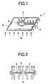
- Fig. 1is a perspective view showing the appearance of the magnetic flux converger 1
- Fig. 2is a cross-sectional view of the magnetic flux converger, showing the flow of alternating magnetic flux.
- the magnetic flux converger 1is constituted by forming a hole 3 in the center of a square conductor plate 2 and forming a cutout 4 so as to extend from the hole 3 to the periphery of the conductor plate 2.
- an eddy current 5develops in the periphery of the conductor plate 2, as shown in Fig. 1.
- the eddy current 5acts on the electromagnetic field so as to prevent the electromagnetic field from entering the conductor plate 2.
- the eddy current 5flows around the hole 3 and the cutout 4 in the direction opposite to that in which the eddy current 5 flows along the periphery.
- the eddy current 5converges magnetic flux ⁇ .
- the converged magnetic fluxcan be converted into voltage.
- the inductance L of a coilis proportional to the square of the winding number of the coil and the area of the coil.
- stray capacitance existing between lines of a coilis substantially proportional to the length of an electric wire of the coil. Hence, the capacitance can be diminished by reducing the diameter of the coil.
- the area of the coilcan be reduced by employment of. the magnetic flux converger 1. Because of the foregoing reasons, reduction in the inductance and capacitance of the coil and rising in the resonance frequency of the coil can be achieved without involvement of reduction in the winding number. If the area of the coil is reduced, the same resonance frequency can be achieved even when the winding number of the coil is increased. Accordingly, for a given electromagnetic field intensity a greater receiving voltage can be achieved.
- the antenna according to the present inventioncomprises a magnetic flux converger 1, an IC chip 10, and an electromagnetic flux converger 20.
- the magnetic flux converger 1is constituted by forming a hole 3 in substantially the center of a square conductor plate 2, and a cutout 4 so as to extend from the hole 3 to a peripheral section of the conductor plate 2.
- the radius of the hole 3is set to a value which is sufficiently smaller than the wavelength of a subject electromagnetic wave.
- a wall-like upright conductor 8is orthogonally coupled on the conductor plate 2 along the periphery thereof, the hole 3, and the cutout 4.
- the upright conductor 8is provided in the portion of the conductor plate 2 through which an eddy current flows intensively, for increasing the area in which the eddy current flows.
- the IC chip 10is constituted of a semiconductor integrated circuit including an amplifier, and a coil 11 is fabricated in a center of an upper face of the IC chip 10.
- the IC chip 10is arranged such that the coil 11 is aligned with the hole 3 of the conductor plate 2.
- the IC chip 10is closely fixed to the lower side of the conductor plate 2 via, e.g., a dielectric layer.
- the electromagnetic flux converger 20is constituted by forming a slot 22 in substantially the center of a conductor plate 21 sufficiently larger than the conductor plate 2.
- a wall-like upright conductor 23is orthogonally coupled on an upper face of the conductor plate 21 along a periphery of a slot 22 through which an eddy current flows intensively.
- the upright conductor 23is provided for increasing the area in which the eddy current flows.
- the outer dimension of the magnetic flux converger 1; that is, the outer dimension of the upright conductor 8, and the inside dimension of the slot 22 of the electromagnetic flux converger 20are set to a value which is about one-half the wavelength of a subject electromagnetic wave.
- the outer periphery of the magnetic flux converger 1 and the inner periphery of the slot 22are formed into substantially the same square.
- the electromagnetic flux converger 20is stacked on the magnetic flux converger 1 in an insulated manner. The above example has described a case where the conductor plate 2 of the magnetic flux converger 1 and the slot 22 of the electromagnetic flux converger 20 are formed into a square.
- the only requirementis that at least one side of the conductor plate 2 and one side of the slot 22 are set to substantially one-half the wavelength of a subject electromagnetic wave.
- the conductor plate 2 and the slot 22are not limited to a square. More specifically, the geometry of the conductor plate 2 of the magnetic flux converger 1 and that of the slot 22 of the electromagnetic flux converger 20 can be set arbitrarily in accordance with the type of polarized wave. Further, even when a superconductor is employed for the magnetic flux converger 1 and the electromagnetic flux converger 20, there is yielded the same result as that yielded when an ordinary conductor is used.
- Fig. 4is a cross-sectional view of Fig. 3.
- Fig. 4the direction in which an external alternating magnetic flux ⁇ is imparted is shown upside down in relation with that shown in Figs. 1 and 2.
- the electromagnetic flux converger 20When an electromagnetic wave considered to be uniform has arrived at the antenna, the electromagnetic flux converger 20 first converges the electromagnetic wave.
- the electromagnetic flux converger 20operates according to the same principle as that of a related slot antenna.
- An electromagnetic fieldis converged into the slot 22 by an eddy current flowing around the slot 22 whose size is one-half the wavelength of the subject electromagnetic wave.
- the upright conductor 23 around the slot 22is provided for reducing electrical resistance against the eddy current.
- the upright conductor 23operates in the same manner as the upright conductor 8 provided in the magnetic flux converger 1.
- the magnetic flux converger 1converges magnetic flux into an area of the hole 3 having a sufficiently smaller diameter than the wavelength of the subject electromagnetic wave received by the magnetic flux converger 1, regardless of the wavelength of the electromagnetic wave.
- the operation of the magnetic flux converger 1is as described with reference to Figs. 1 and 2.
- the upright conductor 8is provided on the conductor plate 2 for increasing an eddy current flowing in the magnetic flux converger 1. The operation of the upright conductor 8 is now be described.
- s2 ⁇ ⁇
- ⁇resistivity of a conductor plate
- ⁇angular velocity
- ⁇permeability of the conductor plate
- the permeability ⁇ of a non-magnetic conductoris substantially equal to the permeability of a vacuum; that is, a value of 4 ⁇ x 10 -7 [H/m].
- conductivity ⁇is 1.6 x 10 -8 [ ⁇ m]. From these values, the skin depth "s" at 100 MHz assumes a value of about 6.4 ⁇ m.
- the electrical resistance R ed of the conductor plate 2 against the eddy currentis defined by the following equation (2).
- R ed⁇ L ed sT
- resistivity ⁇assumes a value of 1.6 x 10 -8 [ ⁇ m].
- the resistance R ed of the conductor plate 2is inversely proportional to the skin depth "s" and the thickness T of the conductor plate.
- the skin depth "s"becomes a fixed value.
- the length L ed of the eddy current flowing pathis defined so as to become substantially proportional to the wavelength of the electromagnetic wave (i.e., the reciprocal of a frequency). Hence, it is evident that the length L ed cannot be reduced greatly.
- the thickness T of the conductor plate 2has a wide range of selection.
- the resistance R ed of the conductor plate 2can be reduced by increasing the thickness T of the conductor plate 2. Reduction in the resistance R ed can be achieved, by increasing the thickness of only an area of the conductor plate 2 in which an eddy current flows.
- the geometry of the upright conductor 8 formed only along the periphery of the conductor plate 2 of the magnetic flux converger 1 and the geometry of the upright conductor 23 formed only along the periphery of the slot 22 of the electromagnetic flux converger 20are preferable.
- the thickness of the upright conductor 8 or that of the upright conductor 23is greater than the skin depth "s."
- the thickness of the upright conductor 8 and 23is preferably several micrometers.
- the upright conductors 8 and 23can be embodied by use of a technique such as electric deposition or electroless deposition.
- conductive materialsuch as copper
- a female mold formed of, e.g., organic materialthrough deposition.
- the manufacturing methodfacilitates setting of the diameter of the hole 3 formed in the magnetic flux converger 1 to a value of 1 mm or less. Further, the dimension of the magnetic flux converger 1 and that of the electromagnetic flux converger 20 become smaller in a higher frequency range, thus requiring a more minute female mold.
- the antennais applied to an electromagnetic wave of, e.g., 30 GHz, one side of the magnetic flux converger 1 assumes a size of 5 mm, and the hole 3 must be finished so as to assume a size of tens of micrometers to hundreds of micrometers.
- the objectiveis achieved by applying a photolithography technique to finishing of the hole 3 through use of a photosensitive plastic film used for manufacturing a printed wiring board.
- the upright conductor 8is provided on the conductor plate 2 of the magnetic flux converger 1
- the upright conductor 23is provided on the conductor plate 21 of the electromagnetic flux converger 20.
- magnetic flux ⁇is converged into the hole 3 formed in the magnetic flux converger 1.
- the thus-converged magnetic fluxpenetrates through the coil 11, thereby producing a voltage across the terminals of the coil 11. It is evident that formation of the coils 11 on a semiconductor integrated circuit results in the following two advantages.
- the first advantageis that the coil 11 can be made small. As is well known, an interconnection having a width of 1 ⁇ m or less can be easily formed on a semiconductor integrated circuit.
- the second advantageis that electrical connection between terminals of the coil 11 and an electric circuit such as an amplifying circuit or a rectifying circuit can be established within processes for fabricating a semiconductor integrated circuit.
- an electric circuitsuch as an amplifying circuit or a rectifying circuit
- the coil 11 and electronic circuitsare formed separately, there is a necessity for use of a connection pad having a side of at least 100 ⁇ m or more for electrically connecting the coil 11 with the electronic circuits.
- electrostatic stray capacitancearises in the connection pad, thereby yielding an adverse influence of reducing the resonance frequency of the coil 11.
- fabricating the coil 11 on a semiconductor integrated circuitobviates operations required for electrical connection.
- an advantage of the antenna according to the present inventionbeing applied to a high frequency range.
- Fig. 5shows an equivalent circuit of the magnetic flux converger 1 and the coil 11.
- a loop A and a loop Bcorrespond to an eddy current flowing path of the magnetic flux converger 1. More specifically, the loop A corresponds to the outer periphery of the conductor plate 2 of the magnetic flux converger 1, and the loop B corresponds to the hole 3 formed in the conductor plate 2.
- the loop B and the coil 11are magnetically coupled together. It is obvious that the loop B and the coil 11 operate in a manner equivalent to that of a transformer. At this time, provided that the loop B serving as a primary winding has one turn and that the coil 11 has N turns, the voltage developing across the coil 11 becomes N times that of the loop B. Accordingly, if a large number is selected for the winding number N of the coil 11, the sensitivity of the antenna can be increased.
- the winding number Ncannot be increased without limitation, because a resonance frequency f c (defined by the inductance L of the coil 11, by the capacitance 'C of the coil 11, and by the capacitance C of the electrostatic stray capacitance 31 of an electric circuit including the coil 11) must be made higher than a frequency f r to be received by the antenna.
- a resonance frequency f cdefined by the inductance L of the coil 11, by the capacitance 'C of the coil 11, and by the capacitance C of the electrostatic stray capacitance 31 of an electric circuit including the coil 11
- a resonance frequency f cdefined by the inductance L of the coil 11, by the capacitance 'C of the coil 11, and by the capacitance C of the electrostatic stray capacitance 31 of an electric circuit including the coil 11
- line capacitance of the coil 11is substantially proportional to the product of the line length of the coil and (N-1)/N.
- the line capacitanceis approximately proportional to the line length of the coil.
- the electrostatic stray capacitance 31 between the coil 11 and the conductor plate 2is proportional to the line length of the coil 11. Accordingly, it is analogously thought that the total capacitance C of the electrostatic stray capacitance 31 is proportional to the length of the line.
- reference numeral 32designates load resistance; e.g., input impedance of an amplifying circuit.
- the resonance frequency f cis inversely proportional to (N ⁇ r) 3/2 . The result shows that the radius "r" of the coil 11 must be made smaller in order to increase the resonance frequency f c of the coil 11 having a large winding number N.
- k 1 and k 2denote coefficients
- Ndenotes the winding number of a coil
- rdenotes the radius of the coil.
- the radius of the hole 3 of the magnetic flux converger 1is selected so as to become considerably smaller than the wavelength of an electromagnetic wave. Hence, the winding number N of the coil 11 can be increased without involvement of drop in the resonance frequency f c of the coil 11.
- the first embodimenthas described the antenna to which is applied the magnetic flux converger 1 constituted of an electrically-continuous single conductor plate 2, the principle of the gist of the present invention is not limited to the embodiment. As shown in Fig. 6, it is evident that an electrically-divided conductor plates 2 may be employed.
- Fig. 6Ashows that two conductor plates 2' are arranged symmetrically, wherein each conductor plate 2' measures a half wavelength x a quarter wavelength.
- an equivalent hole 3'is formed by denting the center of the sides of the two conductor plates 2' where they meet each other.
- the eddy current 5flows in a single direction in the two conductor plates 2'.
- the area where the dents oppose each otheracts as the equivalent hole 3'.
- a third embodiment of the present inventionwill now be described.
- a plurality of antennas according to the present inventionare arranged in a manner as shown in Fig. 7.
- Fig. 7is an equivalent circuit representing a state that a plurality of antennas are interconnected.
- a plate electrode called a patchis placed in a position corresponding to the slot 22 of the electromagnetic flux converger 20 shown in Fig. 3, thus constituting a set of antenna.
- a plurality of antenna setsare used in an arranged manner for receiving satellite broadcast, for example. In this case, patch voltages of the individual patches cannot be added together. Hence, the antennas are connected in parallel with each other for the purpose of supplying heavy power to a load of low impedance.
- the coil 11 of the antenna according to the present inventionoperates independently of a ground-plane potential.
- a plurality of coils 11 and 11' of antennasare connected in series, as shown in Fig. 7, thereby enabling addition of voltages developing in the coils 11 and 11'.
- One methodis to match the length of a wire of the coil 11 with that of a wire of the coil 11' at a point where the voltage of the coil 11 and that of the coil 11' are added together.
- Another methodis to connect the two coils 11 and 11' together via a delay line 38, as shown in Fig. 7. After the phase of a voltage has been shifted 360° relative to the phase of a voltage output from a coil having no delay through use of the delay line 33, the voltages of the two coils are added together.
- the speed of signals propagating in a printed wiring boardis slightly greater than half light speed. Since the magnetic flux converger 1 has a size of a half of the wavelength of the electromagnetic wave, the objective can be achieved by electrically interconnecting the magnetic flux converger 1 and the coil 11 via the printed wiring board such that an interval between the magnetic flux converger 1 and the coil 11 is set so as to be slightly greater than the size. If the winding direction of the coil 11 is made opposite to that of the coil 11', the phase of the voltage output from the coil 11 becomes 180° out of phase with that of the voltage output from the coil 11'. Hence, a delay line for shifting a phase through only 180° may be adopted as the delay line 33.
- a dipole antenna thereofwas replaced with the magnetic flux converger 1 according to the present invention. Further, the coil 11 having two turns was employed. Results of detection tests were performed through use of the thus-modified antenna and a commercially-available Yagi antenna. The test results show that the modified antenna acquired a voltage sensitivity of 5.7 dB (i.e., 1.8 times as large as that obtained by a commercially-available Yagi antenna).
- the dipole antenna of a standard Yagi antennacan be deemed as a single-turn coil. It can be understood that the sensitivity has been increased substantially proportional to an increase in the winding number of the coil.
- the electromagnetic flux converger 20is not limited to a planar structure shown in Fig. 3 but may be embodied as a wave director employed in a standard Yagi antenna.
- the IC chip 10may be replaced with a semiconductor chip having formed therein a rectification diode or a rectification diode bridge.
- the IC chip 10may be replaced with a semiconductor chip provided as a transponder which communicate power with a reader antenna while modulation is performed.
- an electromagnetic waveis converged by magnetic flux converger constituted of a conductor plate.
- the thus-converged magnetic fluxis converted into voltage by a coil.
- the area of the coilcan be reduced, and the winding number of the coil can be increased without involvement of drop in resonance frequency.
- an antenna of high voltage sensitivityMagnetic material is not used for magnetic flux converger, and an eddy current effect of a conductor appearing in a wide range of frequency is utilized.
- the antennacan be applied to a frequency range from hundreds of kHz to tens of GHz.
Landscapes
- Aerials With Secondary Devices (AREA)
- Waveguide Aerials (AREA)
- Details Of Aerials (AREA)
- Variable-Direction Aerials And Aerial Arrays (AREA)
Abstract

Description
Claims (15)
- An antenna, comprising:a converger, including a conductor which converges a magnetic fluxof an electromagnetic wave; anda converter, which coverts the converged magnetic flux into voltage.
- The antenna as set forth in claim 1, wherein:a through hole into which the magnetic flux is converged is formed ata center portion of the conductor; anda cutout is formed so as to extend from a part of the through hole toan outer periphery of the conductor.
- The antenna as set forth in claim 2, wherein the converger includes aresistance reducer provided on at least a peripheral. portion of the conductor toreduce resistance against current flowing in the conductor.
- The antenna as set forth in claim 2, wherein the conductor plate iscomposed of a plurality of sub-plates.
- The antenna as set forth in claim 1, wherein the converter is providedas a coil.
- The antenna as set forth in claim 1, wherein the converter has a sizewhich is sufficiently smaller than a wavelength of the electromagnetic wave.
- The antenna as set forth in claim 5, wherein a winding number of thecoil is two or more.
- The antenna as set forth in claim 1, wherein the converter is formedon a semiconductor integrated circuit.
- An antenna for communicating an electromagnetic wave, comprising:a first converger, which converges the electromagnetic wave;a second converger, which faces the first converger and includes aconductor plate having a through hole, into which a magnetic flux of theconverged electromagnetic wave is converged, formed at a center portionthereof so as to have a size which is sufficiently smaller than a wavelength ofthe electromagnetic wave, and a cutout extending from a part of the throughhole to an outer periphery of the conductor plate; anda converter, which faces the through hole of the conductor plate toconvert the converged magnetic flux into voltage.
- The antenna as set forth in claim 9, wherein the second convergerincludes an upright conductor formed along an outer peripheral portion of theconductor plate, the through hole and the cutout, so as to extend in anorthogonal direction of a direction in which the conductor plate extends.
- The antenna as set forth in claim 9, wherein the first convergerincludes a conductor plate having a slot formed at a center portion thereof andan upright conductor formed along an outer periphery of the conductor plate soas to extend in an orthogonal direction of a direction in which the conductorplate extends.
- The antenna as set forth in claim 11, wherein each of the slot of thefirst converger and the outer periphery of the conductor plate of the secondconverger has a linear portion whose dimension is substantially a half of awavelength of the electromagnetic wave.
- The antenna as set forth in claim 9, wherein the converter is providedas a coil.
- An antenna, comprising;a plurality of antenna elements, interconnected with each other, eachantenna element including:a converger, including a conductor which converges amagnetic flux of an electromagnetic wave; anda converter, which coverts the converged magnetic flux intovoltage.
- The antenna as set forth in claim 14, wherein the antenna elementsare interconnected such that voltages outputted from the respective convertersare added.
Applications Claiming Priority (2)
| Application Number | Priority Date | Filing Date | Title |
|---|---|---|---|
| JP2000297604 | 2000-09-28 | ||
| JP2000297604AJP3481575B2 (en) | 2000-09-28 | 2000-09-28 | antenna |
Publications (3)
| Publication Number | Publication Date |
|---|---|
| EP1193793A2true EP1193793A2 (en) | 2002-04-03 |
| EP1193793A3 EP1193793A3 (en) | 2004-03-03 |
| EP1193793B1 EP1193793B1 (en) | 2006-02-08 |
Family
ID=18779697
Family Applications (1)
| Application Number | Title | Priority Date | Filing Date |
|---|---|---|---|
| EP01123470AExpired - LifetimeEP1193793B1 (en) | 2000-09-28 | 2001-09-28 | Antenna |
Country Status (4)
| Country | Link |
|---|---|
| US (1) | US6861992B2 (en) |
| EP (1) | EP1193793B1 (en) |
| JP (1) | JP3481575B2 (en) |
| DE (1) | DE60117080T2 (en) |
Cited By (60)
| Publication number | Priority date | Publication date | Assignee | Title |
|---|---|---|---|---|
| US8228765B2 (en) | 2006-06-30 | 2012-07-24 | Murata Manufacturing Co., Ltd. | Optical disc |
| US8299929B2 (en) | 2006-09-26 | 2012-10-30 | Murata Manufacturing Co., Ltd. | Inductively coupled module and item with inductively coupled module |
| US8336786B2 (en) | 2010-03-12 | 2012-12-25 | Murata Manufacturing Co., Ltd. | Wireless communication device and metal article |
| US8381997B2 (en) | 2009-06-03 | 2013-02-26 | Murata Manufacturing Co., Ltd. | Radio frequency IC device and method of manufacturing the same |
| US8400365B2 (en) | 2009-11-20 | 2013-03-19 | Murata Manufacturing Co., Ltd. | Antenna device and mobile communication terminal |
| US8413907B2 (en) | 2007-07-17 | 2013-04-09 | Murata Manufacturing Co., Ltd. | Wireless IC device and electronic apparatus |
| US8424769B2 (en) | 2010-07-08 | 2013-04-23 | Murata Manufacturing Co., Ltd. | Antenna and RFID device |
| US8424762B2 (en) | 2007-04-14 | 2013-04-23 | Murata Manufacturing Co., Ltd. | Wireless IC device and component for wireless IC device |
| US8531346B2 (en) | 2007-04-26 | 2013-09-10 | Murata Manufacturing Co., Ltd. | Wireless IC device |
| US8544759B2 (en) | 2009-01-09 | 2013-10-01 | Murata Manufacturing., Ltd. | Wireless IC device, wireless IC module and method of manufacturing wireless IC module |
| US8552870B2 (en) | 2007-07-09 | 2013-10-08 | Murata Manufacturing Co., Ltd. | Wireless IC device |
| US8590797B2 (en) | 2008-05-21 | 2013-11-26 | Murata Manufacturing Co., Ltd. | Wireless IC device |
| EP2424042A4 (en)* | 2009-04-21 | 2013-11-27 | Murata Manufacturing Co | ANTENNA APPARATUS |
| US8602310B2 (en) | 2010-03-03 | 2013-12-10 | Murata Manufacturing Co., Ltd. | Radio communication device and radio communication terminal |
| US8613395B2 (en) | 2011-02-28 | 2013-12-24 | Murata Manufacturing Co., Ltd. | Wireless communication device |
| US8676117B2 (en) | 2006-01-19 | 2014-03-18 | Murata Manufacturing Co., Ltd. | Wireless IC device and component for wireless IC device |
| US8680971B2 (en) | 2009-09-28 | 2014-03-25 | Murata Manufacturing Co., Ltd. | Wireless IC device and method of detecting environmental state using the device |
| US8690070B2 (en) | 2009-04-14 | 2014-04-08 | Murata Manufacturing Co., Ltd. | Wireless IC device component and wireless IC device |
| US8718727B2 (en) | 2009-12-24 | 2014-05-06 | Murata Manufacturing Co., Ltd. | Antenna having structure for multi-angled reception and mobile terminal including the antenna |
| US8720789B2 (en) | 2012-01-30 | 2014-05-13 | Murata Manufacturing Co., Ltd. | Wireless IC device |
| US8740093B2 (en) | 2011-04-13 | 2014-06-03 | Murata Manufacturing Co., Ltd. | Radio IC device and radio communication terminal |
| US8757500B2 (en) | 2007-05-11 | 2014-06-24 | Murata Manufacturing Co., Ltd. | Wireless IC device |
| US8770489B2 (en) | 2011-07-15 | 2014-07-08 | Murata Manufacturing Co., Ltd. | Radio communication device |
| US8797225B2 (en) | 2011-03-08 | 2014-08-05 | Murata Manufacturing Co., Ltd. | Antenna device and communication terminal apparatus |
| US8797148B2 (en) | 2008-03-03 | 2014-08-05 | Murata Manufacturing Co., Ltd. | Radio frequency IC device and radio communication system |
| US8810456B2 (en) | 2009-06-19 | 2014-08-19 | Murata Manufacturing Co., Ltd. | Wireless IC device and coupling method for power feeding circuit and radiation plate |
| US8814056B2 (en) | 2011-07-19 | 2014-08-26 | Murata Manufacturing Co., Ltd. | Antenna device, RFID tag, and communication terminal apparatus |
| US8847831B2 (en) | 2009-07-03 | 2014-09-30 | Murata Manufacturing Co., Ltd. | Antenna and antenna module |
| US8853549B2 (en) | 2009-09-30 | 2014-10-07 | Murata Manufacturing Co., Ltd. | Circuit substrate and method of manufacturing same |
| US8870077B2 (en) | 2008-08-19 | 2014-10-28 | Murata Manufacturing Co., Ltd. | Wireless IC device and method for manufacturing same |
| US8878739B2 (en) | 2011-07-14 | 2014-11-04 | Murata Manufacturing Co., Ltd. | Wireless communication device |
| US8905296B2 (en) | 2011-12-01 | 2014-12-09 | Murata Manufacturing Co., Ltd. | Wireless integrated circuit device and method of manufacturing the same |
| US8917211B2 (en) | 2008-11-17 | 2014-12-23 | Murata Manufacturing Co., Ltd. | Antenna and wireless IC device |
| US8937576B2 (en) | 2011-04-05 | 2015-01-20 | Murata Manufacturing Co., Ltd. | Wireless communication device |
| US8944335B2 (en) | 2010-09-30 | 2015-02-03 | Murata Manufacturing Co., Ltd. | Wireless IC device |
| US8981906B2 (en) | 2010-08-10 | 2015-03-17 | Murata Manufacturing Co., Ltd. | Printed wiring board and wireless communication system |
| US8991713B2 (en) | 2011-01-14 | 2015-03-31 | Murata Manufacturing Co., Ltd. | RFID chip package and RFID tag |
| US9024837B2 (en) | 2010-03-31 | 2015-05-05 | Murata Manufacturing Co., Ltd. | Antenna and wireless communication device |
| US9024725B2 (en) | 2009-11-04 | 2015-05-05 | Murata Manufacturing Co., Ltd. | Communication terminal and information processing system |
| US9104950B2 (en) | 2009-01-30 | 2015-08-11 | Murata Manufacturing Co., Ltd. | Antenna and wireless IC device |
| US9117157B2 (en) | 2009-10-02 | 2015-08-25 | Murata Manufacturing Co., Ltd. | Wireless IC device and electromagnetic coupling module |
| US9166291B2 (en) | 2010-10-12 | 2015-10-20 | Murata Manufacturing Co., Ltd. | Antenna device and communication terminal apparatus |
| US9165239B2 (en) | 2006-04-26 | 2015-10-20 | Murata Manufacturing Co., Ltd. | Electromagnetic-coupling-module-attached article |
| US9178279B2 (en) | 2009-11-04 | 2015-11-03 | Murata Manufacturing Co., Ltd. | Wireless IC tag, reader-writer, and information processing system |
| US9236651B2 (en) | 2010-10-21 | 2016-01-12 | Murata Manufacturing Co., Ltd. | Communication terminal device |
| US9281873B2 (en) | 2008-05-26 | 2016-03-08 | Murata Manufacturing Co., Ltd. | Wireless IC device system and method of determining authenticity of wireless IC device |
| CN105680157A (en)* | 2014-12-04 | 2016-06-15 | Tdk株式会社 | Antenna device and portable electronic device using the same |
| US9378452B2 (en) | 2011-05-16 | 2016-06-28 | Murata Manufacturing Co., Ltd. | Radio IC device |
| US9444143B2 (en) | 2009-10-16 | 2016-09-13 | Murata Manufacturing Co., Ltd. | Antenna and wireless IC device |
| US9460376B2 (en) | 2007-07-18 | 2016-10-04 | Murata Manufacturing Co., Ltd. | Radio IC device |
| US9461363B2 (en) | 2009-11-04 | 2016-10-04 | Murata Manufacturing Co., Ltd. | Communication terminal and information processing system |
| US9460320B2 (en) | 2009-10-27 | 2016-10-04 | Murata Manufacturing Co., Ltd. | Transceiver and radio frequency identification tag reader |
| US9543642B2 (en) | 2011-09-09 | 2017-01-10 | Murata Manufacturing Co., Ltd. | Antenna device and wireless device |
| US9558384B2 (en) | 2010-07-28 | 2017-01-31 | Murata Manufacturing Co., Ltd. | Antenna apparatus and communication terminal instrument |
| US9692128B2 (en) | 2012-02-24 | 2017-06-27 | Murata Manufacturing Co., Ltd. | Antenna device and wireless communication device |
| US9727765B2 (en) | 2010-03-24 | 2017-08-08 | Murata Manufacturing Co., Ltd. | RFID system including a reader/writer and RFID tag |
| US9761923B2 (en) | 2011-01-05 | 2017-09-12 | Murata Manufacturing Co., Ltd. | Wireless communication device |
| US10013650B2 (en) | 2010-03-03 | 2018-07-03 | Murata Manufacturing Co., Ltd. | Wireless communication module and wireless communication device |
| US10235544B2 (en) | 2012-04-13 | 2019-03-19 | Murata Manufacturing Co., Ltd. | Inspection method and inspection device for RFID tag |
| US11354558B2 (en) | 2013-01-18 | 2022-06-07 | Amatech Group Limited | Contactless smartcards with coupling frames |
Families Citing this family (49)
| Publication number | Priority date | Publication date | Assignee | Title |
|---|---|---|---|---|
| JP4143340B2 (en)* | 2002-06-17 | 2008-09-03 | 日立マクセル株式会社 | Non-contact communication type information carrier |
| KR102593172B1 (en)* | 2016-10-05 | 2023-10-24 | 삼성전자 주식회사 | Electronic device having loop antenna |
| JP4922845B2 (en)* | 2007-06-19 | 2012-04-25 | 株式会社エヌ・ティ・ティ・ドコモ | Loop antenna mounting device |
| US9232893B2 (en) | 2009-03-09 | 2016-01-12 | Nucurrent, Inc. | Method of operation of a multi-layer-multi-turn structure for high efficiency wireless communication |
| US11476566B2 (en) | 2009-03-09 | 2022-10-18 | Nucurrent, Inc. | Multi-layer-multi-turn structure for high efficiency wireless communication |
| US9439287B2 (en) | 2009-03-09 | 2016-09-06 | Nucurrent, Inc. | Multi-layer wire structure for high efficiency wireless communication |
| US9208942B2 (en)* | 2009-03-09 | 2015-12-08 | Nucurrent, Inc. | Multi-layer-multi-turn structure for high efficiency wireless communication |
| US9300046B2 (en) | 2009-03-09 | 2016-03-29 | Nucurrent, Inc. | Method for manufacture of multi-layer-multi-turn high efficiency inductors |
| US9306358B2 (en) | 2009-03-09 | 2016-04-05 | Nucurrent, Inc. | Method for manufacture of multi-layer wire structure for high efficiency wireless communication |
| US9444213B2 (en) | 2009-03-09 | 2016-09-13 | Nucurrent, Inc. | Method for manufacture of multi-layer wire structure for high efficiency wireless communication |
| WO2011129151A1 (en)* | 2010-04-12 | 2011-10-20 | 株式会社村田製作所 | Antenna device and communication terminal device |
| US8412276B2 (en)* | 2010-05-24 | 2013-04-02 | Tdk Corporation | Proximity type antenna and radio communication device |
| KR101403681B1 (en)* | 2010-05-28 | 2014-06-09 | 삼성전자주식회사 | Loop antenna |
| JP5924006B2 (en)* | 2012-02-02 | 2016-05-25 | 株式会社村田製作所 | Antenna device |
| JP5772868B2 (en)* | 2012-05-21 | 2015-09-02 | 株式会社村田製作所 | ANTENNA DEVICE AND WIRELESS COMMUNICATION DEVICE |
| CN103918125B (en)* | 2012-09-26 | 2017-03-08 | 株式会社村田制作所 | Antenna assembly and possesses the electronic equipment of antenna assembly |
| CN104094468B (en)* | 2012-12-21 | 2016-01-20 | 株式会社村田制作所 | Interface unit and computer |
| EP2838157A1 (en) | 2013-08-14 | 2015-02-18 | Samsung Electro-Mechanics Co., Ltd. | Cover for electronic device, antenna assembly, electronic device, and method for manufacturing the same |
| US9461500B2 (en)* | 2013-11-21 | 2016-10-04 | Htc Corporation | Wireless charging receiving device and wireless charging system using the same |
| DE112014006211T5 (en)* | 2014-01-20 | 2016-11-10 | Murata Manufacturing Co., Ltd. | antenna component |
| US10186753B2 (en) | 2014-01-31 | 2019-01-22 | Tdk Corporation | Antenna device and portable electronic device using the same |
| US10290934B2 (en) | 2014-04-30 | 2019-05-14 | Tdk Corporation | Antenna device |
| KR101681409B1 (en)* | 2015-04-16 | 2016-12-12 | 삼성전기주식회사 | Coil electronic component |
| US10636563B2 (en) | 2015-08-07 | 2020-04-28 | Nucurrent, Inc. | Method of fabricating a single structure multi mode antenna for wireless power transmission using magnetic field coupling |
| US9941743B2 (en) | 2015-08-07 | 2018-04-10 | Nucurrent, Inc. | Single structure multi mode antenna having a unitary body construction for wireless power transmission using magnetic field coupling |
| US9941590B2 (en) | 2015-08-07 | 2018-04-10 | Nucurrent, Inc. | Single structure multi mode antenna for wireless power transmission using magnetic field coupling having magnetic shielding |
| US10658847B2 (en) | 2015-08-07 | 2020-05-19 | Nucurrent, Inc. | Method of providing a single structure multi mode antenna for wireless power transmission using magnetic field coupling |
| US9948129B2 (en) | 2015-08-07 | 2018-04-17 | Nucurrent, Inc. | Single structure multi mode antenna for wireless power transmission using magnetic field coupling having an internal switch circuit |
| US9960628B2 (en) | 2015-08-07 | 2018-05-01 | Nucurrent, Inc. | Single structure multi mode antenna having a single layer structure with coils on opposing sides for wireless power transmission using magnetic field coupling |
| US10063100B2 (en) | 2015-08-07 | 2018-08-28 | Nucurrent, Inc. | Electrical system incorporating a single structure multimode antenna for wireless power transmission using magnetic field coupling |
| US9941729B2 (en) | 2015-08-07 | 2018-04-10 | Nucurrent, Inc. | Single layer multi mode antenna for wireless power transmission using magnetic field coupling |
| US11205848B2 (en) | 2015-08-07 | 2021-12-21 | Nucurrent, Inc. | Method of providing a single structure multi mode antenna having a unitary body construction for wireless power transmission using magnetic field coupling |
| US9960629B2 (en) | 2015-08-07 | 2018-05-01 | Nucurrent, Inc. | Method of operating a single structure multi mode antenna for wireless power transmission using magnetic field coupling |
| US10985465B2 (en) | 2015-08-19 | 2021-04-20 | Nucurrent, Inc. | Multi-mode wireless antenna configurations |
| US20180062434A1 (en) | 2016-08-26 | 2018-03-01 | Nucurrent, Inc. | Wireless Connector Receiver Module Circuit |
| WO2018101013A1 (en)* | 2016-12-02 | 2018-06-07 | 株式会社村田製作所 | Auxiliary antenna, rfid system, and method for reading rfid tag |
| US10432031B2 (en) | 2016-12-09 | 2019-10-01 | Nucurrent, Inc. | Antenna having a substrate configured to facilitate through-metal energy transfer via near field magnetic coupling |
| US11502547B2 (en) | 2017-02-13 | 2022-11-15 | Nucurrent, Inc. | Wireless electrical energy transmission system with transmitting antenna having magnetic field shielding panes |
| US11283295B2 (en) | 2017-05-26 | 2022-03-22 | Nucurrent, Inc. | Device orientation independent wireless transmission system |
| US11271430B2 (en) | 2019-07-19 | 2022-03-08 | Nucurrent, Inc. | Wireless power transfer system with extended wireless charging range |
| US11227712B2 (en) | 2019-07-19 | 2022-01-18 | Nucurrent, Inc. | Preemptive thermal mitigation for wireless power systems |
| US11056922B1 (en) | 2020-01-03 | 2021-07-06 | Nucurrent, Inc. | Wireless power transfer system for simultaneous transfer to multiple devices |
| US11283303B2 (en) | 2020-07-24 | 2022-03-22 | Nucurrent, Inc. | Area-apportioned wireless power antenna for maximized charging volume |
| US11876386B2 (en) | 2020-12-22 | 2024-01-16 | Nucurrent, Inc. | Detection of foreign objects in large charging volume applications |
| US11881716B2 (en) | 2020-12-22 | 2024-01-23 | Nucurrent, Inc. | Ruggedized communication for wireless power systems in multi-device environments |
| US11695302B2 (en)* | 2021-02-01 | 2023-07-04 | Nucurrent, Inc. | Segmented shielding for wide area wireless power transmitter |
| US12003116B2 (en) | 2022-03-01 | 2024-06-04 | Nucurrent, Inc. | Wireless power transfer system for simultaneous transfer to multiple devices with cross talk and interference mitigation |
| US11831174B2 (en) | 2022-03-01 | 2023-11-28 | Nucurrent, Inc. | Cross talk and interference mitigation in dual wireless power transmitter |
| CN116632518A (en)* | 2023-06-14 | 2023-08-22 | 北京理工大学 | Fully Polarized High-Gain Broadband Conformal Antenna |
Family Cites Families (9)
| Publication number | Priority date | Publication date | Assignee | Title |
|---|---|---|---|---|
| BE482157A (en)* | 1938-12-13 | |||
| GB1207595A (en)* | 1968-03-25 | 1970-10-07 | Pye Ltd | Aerials |
| EP0221694A3 (en) | 1985-10-29 | 1988-06-01 | Toyota Jidosha Kabushiki Kaisha | Vehicle antenna system |
| GB9004431D0 (en)* | 1990-02-28 | 1990-04-25 | Scient Generics Ltd | Detection system for security systems |
| US5223851A (en)* | 1991-06-05 | 1993-06-29 | Trovan Limited | Apparatus for facilitating interconnection of antenna lead wires to an integrated circuit and encapsulating the assembly to form an improved miniature transponder device |
| US5432518A (en) | 1993-06-15 | 1995-07-11 | Texas Instruments Incorporated | Closed slot antenna having outer and inner magnetic loops |
| DE4407116A1 (en) | 1994-03-04 | 1995-09-14 | Lacher Erich Uhren | Long wave ferrite antenna |
| US5495259A (en)* | 1994-03-31 | 1996-02-27 | Lyasko; Gennady | Compact parametric antenna |
| US5826178A (en)* | 1996-01-29 | 1998-10-20 | Seiko Communications Systems, Inc. | Loop antenna with reduced electrical field sensitivity |
- 2000
- 2000-09-28JPJP2000297604Apatent/JP3481575B2/ennot_activeExpired - Fee Related
- 2001
- 2001-09-28DEDE60117080Tpatent/DE60117080T2/ennot_activeExpired - Lifetime
- 2001-09-28USUS09/964,410patent/US6861992B2/ennot_activeExpired - Fee Related
- 2001-09-28EPEP01123470Apatent/EP1193793B1/ennot_activeExpired - Lifetime
Cited By (74)
| Publication number | Priority date | Publication date | Assignee | Title |
|---|---|---|---|---|
| US8725071B2 (en) | 2006-01-19 | 2014-05-13 | Murata Manufacturing Co., Ltd. | Wireless IC device and component for wireless IC device |
| US8676117B2 (en) | 2006-01-19 | 2014-03-18 | Murata Manufacturing Co., Ltd. | Wireless IC device and component for wireless IC device |
| US9165239B2 (en) | 2006-04-26 | 2015-10-20 | Murata Manufacturing Co., Ltd. | Electromagnetic-coupling-module-attached article |
| US8228765B2 (en) | 2006-06-30 | 2012-07-24 | Murata Manufacturing Co., Ltd. | Optical disc |
| US8299929B2 (en) | 2006-09-26 | 2012-10-30 | Murata Manufacturing Co., Ltd. | Inductively coupled module and item with inductively coupled module |
| US8424762B2 (en) | 2007-04-14 | 2013-04-23 | Murata Manufacturing Co., Ltd. | Wireless IC device and component for wireless IC device |
| US8531346B2 (en) | 2007-04-26 | 2013-09-10 | Murata Manufacturing Co., Ltd. | Wireless IC device |
| US8757500B2 (en) | 2007-05-11 | 2014-06-24 | Murata Manufacturing Co., Ltd. | Wireless IC device |
| US8662403B2 (en) | 2007-07-04 | 2014-03-04 | Murata Manufacturing Co., Ltd. | Wireless IC device and component for wireless IC device |
| US8552870B2 (en) | 2007-07-09 | 2013-10-08 | Murata Manufacturing Co., Ltd. | Wireless IC device |
| US8413907B2 (en) | 2007-07-17 | 2013-04-09 | Murata Manufacturing Co., Ltd. | Wireless IC device and electronic apparatus |
| US9460376B2 (en) | 2007-07-18 | 2016-10-04 | Murata Manufacturing Co., Ltd. | Radio IC device |
| US9830552B2 (en) | 2007-07-18 | 2017-11-28 | Murata Manufacturing Co., Ltd. | Radio IC device |
| US8797148B2 (en) | 2008-03-03 | 2014-08-05 | Murata Manufacturing Co., Ltd. | Radio frequency IC device and radio communication system |
| US8590797B2 (en) | 2008-05-21 | 2013-11-26 | Murata Manufacturing Co., Ltd. | Wireless IC device |
| US8973841B2 (en) | 2008-05-21 | 2015-03-10 | Murata Manufacturing Co., Ltd. | Wireless IC device |
| US9022295B2 (en) | 2008-05-21 | 2015-05-05 | Murata Manufacturing Co., Ltd. | Wireless IC device |
| US9281873B2 (en) | 2008-05-26 | 2016-03-08 | Murata Manufacturing Co., Ltd. | Wireless IC device system and method of determining authenticity of wireless IC device |
| US8870077B2 (en) | 2008-08-19 | 2014-10-28 | Murata Manufacturing Co., Ltd. | Wireless IC device and method for manufacturing same |
| US8917211B2 (en) | 2008-11-17 | 2014-12-23 | Murata Manufacturing Co., Ltd. | Antenna and wireless IC device |
| US8544759B2 (en) | 2009-01-09 | 2013-10-01 | Murata Manufacturing., Ltd. | Wireless IC device, wireless IC module and method of manufacturing wireless IC module |
| US9104950B2 (en) | 2009-01-30 | 2015-08-11 | Murata Manufacturing Co., Ltd. | Antenna and wireless IC device |
| US8690070B2 (en) | 2009-04-14 | 2014-04-08 | Murata Manufacturing Co., Ltd. | Wireless IC device component and wireless IC device |
| US8876010B2 (en) | 2009-04-14 | 2014-11-04 | Murata Manufacturing Co., Ltd | Wireless IC device component and wireless IC device |
| US9203157B2 (en) | 2009-04-21 | 2015-12-01 | Murata Manufacturing Co., Ltd. | Antenna device and method of setting resonant frequency of antenna device |
| US9564678B2 (en) | 2009-04-21 | 2017-02-07 | Murata Manufacturing Co., Ltd. | Antenna device and method of setting resonant frequency of antenna device |
| EP2424042A4 (en)* | 2009-04-21 | 2013-11-27 | Murata Manufacturing Co | ANTENNA APPARATUS |
| US9000619B2 (en) | 2009-04-21 | 2015-04-07 | Murata Manufacturing Co., Ltd. | Antenna apparatus |
| US8976075B2 (en) | 2009-04-21 | 2015-03-10 | Murata Manufacturing Co., Ltd. | Antenna device and method of setting resonant frequency of antenna device |
| US8381997B2 (en) | 2009-06-03 | 2013-02-26 | Murata Manufacturing Co., Ltd. | Radio frequency IC device and method of manufacturing the same |
| US8810456B2 (en) | 2009-06-19 | 2014-08-19 | Murata Manufacturing Co., Ltd. | Wireless IC device and coupling method for power feeding circuit and radiation plate |
| US8847831B2 (en) | 2009-07-03 | 2014-09-30 | Murata Manufacturing Co., Ltd. | Antenna and antenna module |
| US8680971B2 (en) | 2009-09-28 | 2014-03-25 | Murata Manufacturing Co., Ltd. | Wireless IC device and method of detecting environmental state using the device |
| US8853549B2 (en) | 2009-09-30 | 2014-10-07 | Murata Manufacturing Co., Ltd. | Circuit substrate and method of manufacturing same |
| US9117157B2 (en) | 2009-10-02 | 2015-08-25 | Murata Manufacturing Co., Ltd. | Wireless IC device and electromagnetic coupling module |
| US9444143B2 (en) | 2009-10-16 | 2016-09-13 | Murata Manufacturing Co., Ltd. | Antenna and wireless IC device |
| US9460320B2 (en) | 2009-10-27 | 2016-10-04 | Murata Manufacturing Co., Ltd. | Transceiver and radio frequency identification tag reader |
| US9024725B2 (en) | 2009-11-04 | 2015-05-05 | Murata Manufacturing Co., Ltd. | Communication terminal and information processing system |
| US9461363B2 (en) | 2009-11-04 | 2016-10-04 | Murata Manufacturing Co., Ltd. | Communication terminal and information processing system |
| US9178279B2 (en) | 2009-11-04 | 2015-11-03 | Murata Manufacturing Co., Ltd. | Wireless IC tag, reader-writer, and information processing system |
| US8704716B2 (en) | 2009-11-20 | 2014-04-22 | Murata Manufacturing Co., Ltd. | Antenna device and mobile communication terminal |
| US8400365B2 (en) | 2009-11-20 | 2013-03-19 | Murata Manufacturing Co., Ltd. | Antenna device and mobile communication terminal |
| US8718727B2 (en) | 2009-12-24 | 2014-05-06 | Murata Manufacturing Co., Ltd. | Antenna having structure for multi-angled reception and mobile terminal including the antenna |
| US10013650B2 (en) | 2010-03-03 | 2018-07-03 | Murata Manufacturing Co., Ltd. | Wireless communication module and wireless communication device |
| US8602310B2 (en) | 2010-03-03 | 2013-12-10 | Murata Manufacturing Co., Ltd. | Radio communication device and radio communication terminal |
| US8336786B2 (en) | 2010-03-12 | 2012-12-25 | Murata Manufacturing Co., Ltd. | Wireless communication device and metal article |
| US8528829B2 (en) | 2010-03-12 | 2013-09-10 | Murata Manufacturing Co., Ltd. | Wireless communication device and metal article |
| US9727765B2 (en) | 2010-03-24 | 2017-08-08 | Murata Manufacturing Co., Ltd. | RFID system including a reader/writer and RFID tag |
| US9024837B2 (en) | 2010-03-31 | 2015-05-05 | Murata Manufacturing Co., Ltd. | Antenna and wireless communication device |
| US8424769B2 (en) | 2010-07-08 | 2013-04-23 | Murata Manufacturing Co., Ltd. | Antenna and RFID device |
| US9558384B2 (en) | 2010-07-28 | 2017-01-31 | Murata Manufacturing Co., Ltd. | Antenna apparatus and communication terminal instrument |
| US8981906B2 (en) | 2010-08-10 | 2015-03-17 | Murata Manufacturing Co., Ltd. | Printed wiring board and wireless communication system |
| US8944335B2 (en) | 2010-09-30 | 2015-02-03 | Murata Manufacturing Co., Ltd. | Wireless IC device |
| US9166291B2 (en) | 2010-10-12 | 2015-10-20 | Murata Manufacturing Co., Ltd. | Antenna device and communication terminal apparatus |
| US9236651B2 (en) | 2010-10-21 | 2016-01-12 | Murata Manufacturing Co., Ltd. | Communication terminal device |
| US9761923B2 (en) | 2011-01-05 | 2017-09-12 | Murata Manufacturing Co., Ltd. | Wireless communication device |
| US8991713B2 (en) | 2011-01-14 | 2015-03-31 | Murata Manufacturing Co., Ltd. | RFID chip package and RFID tag |
| US8613395B2 (en) | 2011-02-28 | 2013-12-24 | Murata Manufacturing Co., Ltd. | Wireless communication device |
| US8757502B2 (en) | 2011-02-28 | 2014-06-24 | Murata Manufacturing Co., Ltd. | Wireless communication device |
| US8960561B2 (en) | 2011-02-28 | 2015-02-24 | Murata Manufacturing Co., Ltd. | Wireless communication device |
| US8797225B2 (en) | 2011-03-08 | 2014-08-05 | Murata Manufacturing Co., Ltd. | Antenna device and communication terminal apparatus |
| US8937576B2 (en) | 2011-04-05 | 2015-01-20 | Murata Manufacturing Co., Ltd. | Wireless communication device |
| US8740093B2 (en) | 2011-04-13 | 2014-06-03 | Murata Manufacturing Co., Ltd. | Radio IC device and radio communication terminal |
| US9378452B2 (en) | 2011-05-16 | 2016-06-28 | Murata Manufacturing Co., Ltd. | Radio IC device |
| US8878739B2 (en) | 2011-07-14 | 2014-11-04 | Murata Manufacturing Co., Ltd. | Wireless communication device |
| US8770489B2 (en) | 2011-07-15 | 2014-07-08 | Murata Manufacturing Co., Ltd. | Radio communication device |
| US8814056B2 (en) | 2011-07-19 | 2014-08-26 | Murata Manufacturing Co., Ltd. | Antenna device, RFID tag, and communication terminal apparatus |
| US9543642B2 (en) | 2011-09-09 | 2017-01-10 | Murata Manufacturing Co., Ltd. | Antenna device and wireless device |
| US8905296B2 (en) | 2011-12-01 | 2014-12-09 | Murata Manufacturing Co., Ltd. | Wireless integrated circuit device and method of manufacturing the same |
| US8720789B2 (en) | 2012-01-30 | 2014-05-13 | Murata Manufacturing Co., Ltd. | Wireless IC device |
| US9692128B2 (en) | 2012-02-24 | 2017-06-27 | Murata Manufacturing Co., Ltd. | Antenna device and wireless communication device |
| US10235544B2 (en) | 2012-04-13 | 2019-03-19 | Murata Manufacturing Co., Ltd. | Inspection method and inspection device for RFID tag |
| US11354558B2 (en) | 2013-01-18 | 2022-06-07 | Amatech Group Limited | Contactless smartcards with coupling frames |
| CN105680157A (en)* | 2014-12-04 | 2016-06-15 | Tdk株式会社 | Antenna device and portable electronic device using the same |
Also Published As
| Publication number | Publication date |
|---|---|
| US20020053992A1 (en) | 2002-05-09 |
| DE60117080T2 (en) | 2006-07-20 |
| JP2002111363A (en) | 2002-04-12 |
| JP3481575B2 (en) | 2003-12-22 |
| DE60117080D1 (en) | 2006-04-20 |
| US6861992B2 (en) | 2005-03-01 |
| EP1193793A3 (en) | 2004-03-03 |
| EP1193793B1 (en) | 2006-02-08 |
Similar Documents
| Publication | Publication Date | Title |
|---|---|---|
| US6861992B2 (en) | Antenna | |
| US9191072B2 (en) | RF identification device with near-field-coupled antenna | |
| US8508429B2 (en) | Radio communication equipment | |
| US7990337B2 (en) | Radio frequency IC device | |
| CN1823447B (en) | Slotted cylinder antenna | |
| US6147655A (en) | Flat loop antenna in a single plane for use in radio frequency identification tags | |
| Edwards et al. | High-efficiency elliptical slot antennas with quartz superstrates for silicon RFICs | |
| US4827266A (en) | Antenna with lumped reactive matching elements between radiator and groundplate | |
| US8400231B2 (en) | High-frequency coupler and communication device | |
| US8797148B2 (en) | Radio frequency IC device and radio communication system | |
| US11367942B2 (en) | Antenna device and IC card having the same | |
| US4318109A (en) | Planar antenna with tightly wound folded sections | |
| US10333198B2 (en) | Antenna apparatus and communication terminal apparatus | |
| US7751793B2 (en) | Integrated structure of inductances with shared values on a semiconductor substrate | |
| US11276909B2 (en) | Nonreciprocal circuit element, manufacturing method of the same, and communication apparatus using the same | |
| EP0506091B1 (en) | CM type directional coupler destined for use as power detector in portable telephone | |
| JP2004064780A (en) | antenna | |
| US6097265A (en) | Millimeter wave polymeric waveguide-to-coax transition | |
| US20220336949A1 (en) | Compact directional antenna, device comprising such an antenna | |
| JPH0229007A (en) | Antenna system | |
| JPH01305603A (en) | Line transformer | |
| CN110600873A (en) | Circularly polarized antenna using ground potential metal plate radiation technology and design method thereof | |
| JPWO2020012726A1 (en) | Wireless communication device and manufacturing method thereof | |
| JP3462635B2 (en) | Microstrip antenna | |
| Kim et al. | Densely Placed Rectenna Array with Decoupling Slots for Enhanced Received Power in Far-Field Wireless Power Transfer |
Legal Events
| Date | Code | Title | Description |
|---|---|---|---|
| PUAI | Public reference made under article 153(3) epc to a published international application that has entered the european phase | Free format text:ORIGINAL CODE: 0009012 | |
| AK | Designated contracting states | Kind code of ref document:A2 Designated state(s):AT BE CH CY DE DK ES FI FR GB GR IE IT LI LU MC NL PT SE TR | |
| AX | Request for extension of the european patent | Free format text:AL;LT;LV;MK;RO;SI | |
| PUAL | Search report despatched | Free format text:ORIGINAL CODE: 0009013 | |
| AK | Designated contracting states | Kind code of ref document:A3 Designated state(s):AT BE CH CY DE DK ES FI FR GB GR IE IT LI LU MC NL PT SE TR | |
| AX | Request for extension of the european patent | Extension state:AL LT LV MK RO SI | |
| RIC1 | Information provided on ipc code assigned before grant | Ipc:7H 01Q 7/00 A | |
| 17P | Request for examination filed | Effective date:20040416 | |
| 17Q | First examination report despatched | Effective date:20040719 | |
| AKX | Designation fees paid | Designated state(s):DE FR GB | |
| GRAP | Despatch of communication of intention to grant a patent | Free format text:ORIGINAL CODE: EPIDOSNIGR1 | |
| RAP1 | Party data changed (applicant data changed or rights of an application transferred) | Owner name:YAGI ANTENNA INC. Owner name:KAWAKAMI, KANJI | |
| GRAS | Grant fee paid | Free format text:ORIGINAL CODE: EPIDOSNIGR3 | |
| GRAA | (expected) grant | Free format text:ORIGINAL CODE: 0009210 | |
| AK | Designated contracting states | Kind code of ref document:B1 Designated state(s):DE FR GB | |
| REG | Reference to a national code | Ref country code:GB Ref legal event code:FG4D | |
| REF | Corresponds to: | Ref document number:60117080 Country of ref document:DE Date of ref document:20060420 Kind code of ref document:P | |
| ET | Fr: translation filed | ||
| PLBE | No opposition filed within time limit | Free format text:ORIGINAL CODE: 0009261 | |
| STAA | Information on the status of an ep patent application or granted ep patent | Free format text:STATUS: NO OPPOSITION FILED WITHIN TIME LIMIT | |
| 26N | No opposition filed | Effective date:20061109 | |
| PGFP | Annual fee paid to national office [announced via postgrant information from national office to epo] | Ref country code:FR Payment date:20100921 Year of fee payment:10 | |
| PGFP | Annual fee paid to national office [announced via postgrant information from national office to epo] | Ref country code:GB Payment date:20100922 Year of fee payment:10 | |
| PGFP | Annual fee paid to national office [announced via postgrant information from national office to epo] | Ref country code:DE Payment date:20100922 Year of fee payment:10 | |
| GBPC | Gb: european patent ceased through non-payment of renewal fee | Effective date:20110928 | |
| REG | Reference to a national code | Ref country code:FR Ref legal event code:ST Effective date:20120531 | |
| REG | Reference to a national code | Ref country code:DE Ref legal event code:R119 Ref document number:60117080 Country of ref document:DE Effective date:20120403 | |
| PG25 | Lapsed in a contracting state [announced via postgrant information from national office to epo] | Ref country code:DE Free format text:LAPSE BECAUSE OF NON-PAYMENT OF DUE FEES Effective date:20120403 | |
| PG25 | Lapsed in a contracting state [announced via postgrant information from national office to epo] | Ref country code:FR Free format text:LAPSE BECAUSE OF NON-PAYMENT OF DUE FEES Effective date:20110930 Ref country code:GB Free format text:LAPSE BECAUSE OF NON-PAYMENT OF DUE FEES Effective date:20110928 |