EP1191596A2 - Semiconductor memory device and its manufacturing method - Google Patents
Semiconductor memory device and its manufacturing methodDownload PDFInfo
- Publication number
- EP1191596A2 EP1191596A2EP01120769AEP01120769AEP1191596A2EP 1191596 A2EP1191596 A2EP 1191596A2EP 01120769 AEP01120769 AEP 01120769AEP 01120769 AEP01120769 AEP 01120769AEP 1191596 A2EP1191596 A2EP 1191596A2
- Authority
- EP
- European Patent Office
- Prior art keywords
- columnar semiconductor
- layer
- layers
- semiconductor layer
- columnar
- Prior art date
- Legal status (The legal status is an assumption and is not a legal conclusion. Google has not performed a legal analysis and makes no representation as to the accuracy of the status listed.)
- Withdrawn
Links
- 239000004065semiconductorSubstances0.000titleclaimsabstractdescription87
- 238000004519manufacturing processMethods0.000titleclaimsdescription33
- 238000009792diffusion processMethods0.000claimsabstractdescription65
- 239000000758substrateSubstances0.000claimsabstractdescription55
- 239000000969carrierSubstances0.000claimsabstractdescription18
- 239000011159matrix materialSubstances0.000claimsabstractdescription3
- XUIMIQQOPSSXEZ-UHFFFAOYSA-NSiliconChemical compound[Si]XUIMIQQOPSSXEZ-UHFFFAOYSA-N0.000claimsdescription79
- 229910052710siliconInorganic materials0.000claimsdescription78
- 239000010703siliconSubstances0.000claimsdescription78
- 238000005530etchingMethods0.000claimsdescription5
- 238000009413insulationMethods0.000claimsdescription5
- 239000012535impuritySubstances0.000claimsdescription3
- 230000005012migrationEffects0.000claimsdescription3
- 238000013508migrationMethods0.000claimsdescription3
- 239000011800void materialSubstances0.000claimsdescription3
- 241000402754Erythranthe moschataSpecies0.000claims1
- 238000000137annealingMethods0.000claims1
- 238000007599dischargingMethods0.000claims1
- 239000010410layerSubstances0.000description133
- VYPSYNLAJGMNEJ-UHFFFAOYSA-NSilicium dioxideChemical compoundO=[Si]=OVYPSYNLAJGMNEJ-UHFFFAOYSA-N0.000description25
- 229910052814silicon oxideInorganic materials0.000description25
- 238000010586diagramMethods0.000description21
- 238000000034methodMethods0.000description15
- 229910052581Si3N4Inorganic materials0.000description12
- HQVNEWCFYHHQES-UHFFFAOYSA-Nsilicon nitrideChemical compoundN12[Si]34N5[Si]62N3[Si]51N64HQVNEWCFYHHQES-UHFFFAOYSA-N0.000description12
- 230000008569processEffects0.000description10
- 230000008878couplingEffects0.000description8
- 238000010168coupling processMethods0.000description8
- 238000005859coupling reactionMethods0.000description8
- 229910021420polycrystalline siliconInorganic materials0.000description8
- 239000003990capacitorSubstances0.000description6
- 239000011229interlayerSubstances0.000description6
- 230000003647oxidationEffects0.000description4
- 238000007254oxidation reactionMethods0.000description4
- 230000003139buffering effectEffects0.000description3
- 230000002349favourable effectEffects0.000description3
- 150000002500ionsChemical class0.000description3
- 238000001459lithographyMethods0.000description3
- 238000003491arrayMethods0.000description2
- 230000015572biosynthetic processEffects0.000description2
- 230000008859changeEffects0.000description2
- 230000007423decreaseEffects0.000description2
- 230000003247decreasing effectEffects0.000description2
- 230000001066destructive effectEffects0.000description2
- 230000000694effectsEffects0.000description2
- 238000002955isolationMethods0.000description2
- 230000002093peripheral effectEffects0.000description2
- 230000000630rising effectEffects0.000description2
- UFHFLCQGNIYNRP-UHFFFAOYSA-NHydrogenChemical compound[H][H]UFHFLCQGNIYNRP-UHFFFAOYSA-N0.000description1
- 238000009825accumulationMethods0.000description1
- 230000003213activating effectEffects0.000description1
- 230000003321amplificationEffects0.000description1
- 239000004020conductorSubstances0.000description1
- 230000003292diminished effectEffects0.000description1
- 230000006870functionEffects0.000description1
- 229910052739hydrogenInorganic materials0.000description1
- 239000001257hydrogenSubstances0.000description1
- 239000002184metalSubstances0.000description1
- 238000003199nucleic acid amplification methodMethods0.000description1
- 239000011295pitchSubstances0.000description1
- 230000001681protective effectEffects0.000description1
- 238000009751slip formingMethods0.000description1
Images


Classifications
- H—ELECTRICITY
- H10—SEMICONDUCTOR DEVICES; ELECTRIC SOLID-STATE DEVICES NOT OTHERWISE PROVIDED FOR
- H10D—INORGANIC ELECTRIC SEMICONDUCTOR DEVICES
- H10D84/00—Integrated devices formed in or on semiconductor substrates that comprise only semiconducting layers, e.g. on Si wafers or on GaAs-on-Si wafers
- H—ELECTRICITY
- H10—SEMICONDUCTOR DEVICES; ELECTRIC SOLID-STATE DEVICES NOT OTHERWISE PROVIDED FOR
- H10D—INORGANIC ELECTRIC SEMICONDUCTOR DEVICES
- H10D30/00—Field-effect transistors [FET]
- H10D30/60—Insulated-gate field-effect transistors [IGFET]
- H10D30/67—Thin-film transistors [TFT]
- H10D30/6729—Thin-film transistors [TFT] characterised by the electrodes
- H10D30/673—Thin-film transistors [TFT] characterised by the electrodes characterised by the shapes, relative sizes or dispositions of the gate electrodes
- H10D30/6735—Thin-film transistors [TFT] characterised by the electrodes characterised by the shapes, relative sizes or dispositions of the gate electrodes having gates fully surrounding the channels, e.g. gate-all-around
- H—ELECTRICITY
- H10—SEMICONDUCTOR DEVICES; ELECTRIC SOLID-STATE DEVICES NOT OTHERWISE PROVIDED FOR
- H10B—ELECTRONIC MEMORY DEVICES
- H10B12/00—Dynamic random access memory [DRAM] devices
- H—ELECTRICITY
- H10—SEMICONDUCTOR DEVICES; ELECTRIC SOLID-STATE DEVICES NOT OTHERWISE PROVIDED FOR
- H10D—INORGANIC ELECTRIC SEMICONDUCTOR DEVICES
- H10D86/00—Integrated devices formed in or on insulating or conducting substrates, e.g. formed in silicon-on-insulator [SOI] substrates or on stainless steel or glass substrates
- H10D86/201—Integrated devices formed in or on insulating or conducting substrates, e.g. formed in silicon-on-insulator [SOI] substrates or on stainless steel or glass substrates the substrates comprising an insulating layer on a semiconductor body, e.g. SOI
- H—ELECTRICITY
- H10—SEMICONDUCTOR DEVICES; ELECTRIC SOLID-STATE DEVICES NOT OTHERWISE PROVIDED FOR
- H10B—ELECTRONIC MEMORY DEVICES
- H10B12/00—Dynamic random access memory [DRAM] devices
- H10B12/01—Manufacture or treatment
- H10B12/02—Manufacture or treatment for one transistor one-capacitor [1T-1C] memory cells
- H10B12/05—Making the transistor
- H10B12/053—Making the transistor the transistor being at least partially in a trench in the substrate
Definitions
- This inventionrelates to a dynamic semiconductor memory device (DRAM) and its manufacturing method.
- DRAMdynamic semiconductor memory device
- each memory cellsis made up of a MOS transistor and a capacitor. Employment of trench capacitor structures and stacked capacitor structures has greatly progressed miniaturization of DRAM.
- a semiconductor memory devicecomprising:
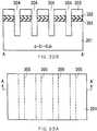
- Fig. 1is a diagram that shows a layout of a DRAM cell array according to an embodiment of the invention
- Figs. 2 and 3are cross-sectional views taken along the A-A' and B-B' lines of Fig. 1, respectively.
- Columnar silicon layersare formed in positions of respective memory cells MC by processing a p-type silicon substrate 1.
- Each memory cell MCis composed of a vertical MOS transistor formed by using the columnar silicon layer 2.
- the transistor of each memory cell MCis an NMOS transistor in which a gate electrode is formed to surround the columnar silicon layer 2 via a gate insulating film 3 and an n + -type source diffusion layer 6 is formed at the bottom.
- This transistor structureis disclosed as so-called “SGT” in the paper “Impact of Surrounding Gate Transistor (SGT) for high density LSI's” by H. Takato et al. (IEEE Transactions on Electron Devices, vol. 38, No. 3, pp. 573-577, March 1991).
- the source diffusion layer 6 formed at the bottom of the columnar silicon layer 2is important for the source diffusion layer 6 formed at the bottom of the columnar silicon layer 2 to lie across the full extent of the bottom of the columnar silicon layer 2 to electrically insulate the p-type region of the columnar silicon layer 2 from the p-type region of the substrate 1.
- the columnar silicon layer 2is held floating and can be controlled in bulk potential to enable dynamic recording operation by one transistor according to the invention, as explained later.
- the source diffusion layer 6is formed to cover the entire surface of the substrate 1 to behave as a fixed potential line SS common to all memory cells MC.
- the gate electrodes 4 surrounding the columnar silicon layer 2are formed of a polycrystalline silicon film.
- word lines (WL) 9commonly connecting the gate electrodes 4 are formed.
- the surface having formed the transistorsis covered by an inter-layer insulating film 7, and bit lines 8 are formed thereon.
- the bit lines 8extend in the direction orthogonal to the word lines 9, and are connected to drain diffusion layers 5 of respective memory cells MC.
- Fig. 4shows a equivalent circuit of this DRAM cell array.
- Each memory cell MCis composed only of a single NMOS transistor. Drains are connected to bit lines BL, gates are connected to word lines WL and sources are commonly connected to a fixed potential line SS.
- sense amplifiers SAare connected in an open bit line system, and a pair of bit lines BL, BBL of cell arrays disposed at opposite sides of each sense amplifier are connected to the sense amplifier SA. Therefore, although not shown, at least one dummy cell is disposed in each of the cell arrays associated with bit lines BL, BBL.
- Operation principle of the DRAM cell mad up of the NMOS transistorutilizes excessive accumulation of holes that are majority carriers in the bulk region (p-type columnar silicon layer 2 insulated and isolated from others) of the MOS transistor. More specifically, a predetermined positive potential is applied to the gate electrode while a large channel current is supplied from the drain diffusion layer 5, thereby to generate hot carriers by impact ionization and have the silicon layer 2 excessively hold holes that are majority carriers of the silicon layer 2.
- the excessive hold storage state(with a higher potential than in the thermal equilibrium state) is determined as data "1", for example.
- the state, in which the pn junction between the drain diffusion layer 5 and the silicon layer 2 is forwardly biased and excessive holes in the silicon layer 2 are released to the drain side,is determined as data "0".
- Data “0” and “1”are different potentials of the bulk region, and they are stored as a difference of threshold voltages of the MOS transistor. That is, threshold voltage Vth1 in the sate of hi potential data "1" of the bulk region by storage of holes is lower than threshold voltage Vth0 in the state of data "0".
- threshold voltage Vth1 in the sate of hi potential data "1" of the bulk region by storage of holesis lower than threshold voltage Vth0 in the state of data "0".
- Vth1 in the sate of hi potential data "1" of the bulk region by storage of holesis lower than threshold voltage Vth0 in the state of data "0".
- a first data read-out methodsupplies the word line WL with a read-out potential that is an intermediate value between the threshold voltages Vth0 and Vth1 of the data "0" and “1", and utilizes the phenomenon that no current flows in memory cells with data "0” but a current flows in memory cells with data "1". More specifically, for example, the bit line BL is precharged to a predetermined potential VBL, and the word line WL is driven later. As a result, as shown in Fig. 6, in case of data "0", no change occurs in the bit line precharge potential VBL, and in case of data "1", the precharge potential VBL decreases.
- a second read-out systemsupplies the bit line BL with a current after activating the word line WL, and utilizes a difference in rising speed of the bit line potential, depending upon conductivities of "0" and "1".
- the bit line BLis precharged to 0 V, and the word line WL is activated as shown in Fig. 7, thereby to supply the bit line current.
- the difference in rising speed of the potential in the bit linedata can be distinguished.
- a third read-out systemreads a difference between bit line currents that are different depending on "0" and "1" when the bit line BL is clamped to a predetermined potential. To read out the current difference, a current-voltage converting circuit is necessary. Finally, however, a sense output is issued through differential amplification of the potential difference.
- write operationis preferably effected by writing pulses for both "0" and "1" to save power consumption.
- FIGs. 8 through 11show waveforms of read/refresh and read/write operations in case of using the first read-out system configured to distinguish data depending on the presence or absence of discharge to the bit line by the selected cell.
- the reference potential given to the fixed potential line SS commonly connecting the sources of all memory cells MCis o V.
- Figs. 8 and 9are waveforms of read/refresh operations of data "1" and data "0", respectively.
- the memoryUp to the time t1, the memory is in the data holding state (non-selected state), and the word line WL is supplied with a negative potential.
- the word line WLis raised to a predetermined positive potential.
- the word line potentialis adjusted to a value between the threshold values Vth0 and Vth1 of data "0" and "1".
- the precharged bit line VBLis becomes a low potential due to a discharge.
- the bit line potential VBLIn case of data "0", the bit line potential VBL is maintained. Thereby, data "1" and "0" are distinguished.
- the word line WLis negatively biased, thereby to complete the read/refresh operations.
- the word lines WLare held in negative potentials, that is, the bulk region is held in a negative potential, no channel current flows, and writing does not occur.
- the word line WLare held in negative potentials, and emission of holes does not occur.
- Figs. 10 and 11are waveforms of read/write operations of data "1" and data "0" by the same read-out system. Read-out operations at the time t1 in Figs. 10 and 11 are the same as those of Figs. 8 and 9, respectively.
- the word line WLis raised to a high potential, and in case of writing data "0" in the same selected cell, a negative potential is simultaneously applied to the bit line BL (Fig. 10).
- a positive potentialis applied to the bit line BL (Fig. 11).
- the drain junctionis forwardly biased, and holes in the bulk region are emitted.
- a channel currentflows, impact ionization occurs, and holes are accumulated in the bulk region.
- the DRAM cell according to the inventionis made of SGT having the floating bulk region electrically isolated from others, and enables realization of the cell size of 4F 2 .
- potential control of the floating bulk regionis attained by using the capacity coupling from the gate electrode, without using back gate control, and the source diffusion layer is fixed in potential as well. That is, control of read/write operations is easily accomplished only by the word line WL and the bit line BL.
- the memory cellis basically can be read in a non-destructive mode, it is not necessary to provide the sense amplifier for each bit line, and layout of the sense amplifiers is easy.
- the current read-out systemit has a resistance to noise, and reading is possible even in the open bit line system.
- the channel regionsurrounds the columnar silicon layer and the channel length is determined by the height of the columnar silicon layer, a large channel length can be obtained independently from the horizontal size determined by lithography. In other words, without increasing the horizontal area, a large channel length can be realized within substantially the same area as the bit line contact. Therefore, capacity coupling between the word line and the bulk region can be increased, and reliable operation control by controlling the bulk potential from the word line is ensured.
- the threshold valuechange largely relative to changes of the bulk potential.
- Thiscan be also realized easily by employing the SGT structure. That is, by producing a concentration profile in the substrate in its thickness direction such that the substrate impurity concentration is high in a central portion of the channel and the channel concentration near the pn junction is low, changes of the threshold value relative to changes of the bulk potential can be enlarged by the substrate biasing effect while minimizing the junction leakage.
- the pn junction capacity connected to the bit linecan be reduced, and this also contributes to relatively increasing the capacity coupling ratio of the word line and the bulk region. Further, as a result, since the bit line capacity also decreases, the charge and discharge current of the bit line capacity upon read and write operations is diminished, and higher speed and lower power consumption are attained thereby.
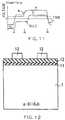
- FIG. 12A concrete manufacturing process of the cell array explained with reference to Figs. 1 through 3 is next explained with reference to Figs. 12 through 17 that are cross-sectional views corresponding to the cross-sectional view of Fig. 2, showing different steps of the manufacturing process.
- a buffering silicon oxide film 11is formed to a thickness around 10 nm on a p-type silicon substrate 1
- a silicon nitride film 12approximately 200 nm thick, is formed thereon, and a resist 13 is formed and patterned thereon by lithography.
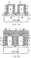
- the silicon nitride film 12 and the silicon oxide film 11are etched, and the silicon substrate 1 is further etched to make channels 14 extending in crossing directions and thereby form the columnar silicon layers 2.
- the resist 13 and the silicon nitride film 12are removed, As ions are implanted, and as shown in Fig. 14, diffusion layers 6, 5 to be used as sources and drains, respectively, are formed on tops of the channels 14 and the columnar silicon layers 2.
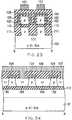
- a gate oxide film 3is formed on and around the columnar silicon layers 2, by thermal oxidation, and a polycrystalline silicon film 40 for forming gate electrodes is formed subsequently.
- the thermal oxidation process including gate oxidation and subsequent thermal processthe n + -type source diffusion layers 6 formed at bottoms of the channels 14 diffuse laterally.
- p-type regions of the columnar silicon layers 2 and p-type regions of the substrate 1are electrically isolated by the source diffusion layer 6.
- the entire surface of the polycrystalline silicon film 40is etched by RIE to form the gate electrodes 4 only on side walls of the columnar silicon layers 2 as shown in Fig. 16, In this etching process, however, spaces between the columnar silicon layers 2 aligned in the direction orthogonal to the sheet of Fig. 16 are covered with a resist. As a result, as shown in figs. 1 and 3, word lines 9 are made of the same polycrystalline silicon film 40 to connect the gate electrodes 4.
- a silicon oxide filmis formed as shown in Fig. 17, and it is leveled by CMP to form the inter-layer insulating film 7.
- an Al filmis formed and patterned to form bit lines 8, as shown in Fig. 2.
- bit lines 8are other metal films of W, etc., for example, instead of the Al film, or films of other conductive materials, such as or polycrystalline silicon.
- an inter-layer insulating filmis formed to make wirings for connection to peripheral circuits.
- the source diffusion layer 6 formed at bottoms of the columnar silicon layers 2is connected to a signal line fixed in potential, such as a grounded line, at a peripheral portion of the cell array.
- the columnar silicon layers 2are completely isolated electrically from the substrate by using lateral diffusion of the source diffusion layer 6. This is easy when the diameter of each columnar silicon layer 2 is sufficiently small, but it is not always easy when the diameter is relatively large. In that case, it is desirable that an n + -type layer to be used as the source diffusion layer 6 is built in the substrate beforehand. That is, a structure as shown in Fig. 18 is previously prepared as the silicon substrate 1.
- This structurecan be obtained, for example, by using a p-type layer 20 as the substrate, then forming an n + -type buried layer 21 on the entire surface of the p-type layer 20, and next epitaxially growing a p-type silicon layer 22.
- the substrate of Fig. 18can be made by preparing independent silicon substrates as the p-type layers 20, 21, then forming the n + -type layer 21 on one of them, and thereafter bonding them directly. Using such an epitaxial substrate or a bonded substrate, once the columnar silicon layers are formed by etching the substrate to the depth of the n + -type layer 21, reliable electric isolation between the columnar silicon layers and the substrate is ensured.
- n + -type layer 6It is not indispensable that bottoms of the columnar silicon layers are completely closed by the n + -type layer 6.
- n + -type layers 6 extending from bottoms of the channelsdo not completely traverse the columnar silicon layers 2, only if the depletion layers 23 extending from portions encircling the columnar silicon layers 2 toward their centers connect to each other under zero bias, p-type regions of the columnar silicon layers 2 and p-type regions of the substrate 1 are electrically isolated.
- Fig. 20shows a cross section of another cell array structure, which corresponds to Fig. 2.
- top portions of the columnar silicon layers 2are tapered to diminish the diameter toward the tops. In this manner, contact area of each drain diffusion layers 5 formed on top ends of the columnar silicon layers 2 with the bit line 8 can be reduced.
- junction between the n*-type source region 6 and the drain diffusion layers 5 with the p-type silicon layer 2is preferably graded junction in which the n + -type layer joins the p-type layer via an n-type layer gradually decreased in concentration, instead of step-like junction. In this manner, junction leakage can be reduced, and the junction capacity can be reduced as well. Even when this junction structure is used, since the height of the columnar silicon layers ensure the channel length, unlike the horizontal transistors, a sufficiently high p-type impurity concentration can be ensured in the central portions of the channels. Therefore, it is convenient for dynamic recording operation by bulk potential control using the gate capacity.
- the first embodimenthas been explained above as using as memory cells MC the transistors having the SGT structure in which side wall surfaces of the columnar silicon layers are used as channel regions.
- the second embodimenthas the transistor shown in Fig. 21. That is, a columnar silicon layer 102 formed on a silicon substrate 101 is used as an active layer, a gate electrode 104 is provided to lie across the columnar silicon layer 102 and oppose to the top surface and opposite side surfaces of the columnar silicon layer 102 via a gate insulating film 103, and drain and source diffusion layers are formed at opposite sides of the gate electrode 104.
- the columnar silicon layer 102is held floating by an insulating film buried at the bottom thereof.
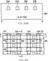
- Fig. 22shows a layout of a DRAM cell according to the instant embodiment
- Figs. 23 and 24are cross-sectional views taken along the A-A' and B-B' lines of Fig. 22.
- used as the columnar silicon layer 102is a p-type silicon layer epitaxially grown on the silicon substrate 101.
- Active layer 102which are convex silicon layers obtained by processing the p-type silicon layer, are arranged in a pattern of a grating such that each drain diffusion layer is shared by active layers 102 of different memory cells MC adjacent to each other in the bit line direction and the source diffusion layer is continuously formed in the word line direction as a common source line.
- each active layer 102a silicon oxide film 110 is buried.
- a silicon oxide film 111is buried also in each device isolating region.
- the gate electrode 104is formed as a word line that lies across the active layer 102 and opposes to its three surfaces.
- the n + -type source and drain diffusion layer 105are formed in self alignment with the gate electrode 104.
- the surface having formed the transistorsis covered with an inter-layer insulating film 106, and bit lines 107 are formed thereon.
- FIG. 25show the cross section corresponding to the cross section shown in Fig. 23.
- the silicon oxide film 110is formed on locations of silicon substrate 101 where silicon layers should be formed later as active regions having a grating pattern, with a certain tolerance for misalignment.
- a p-type silicon layer 1020is epitaxially grown on the silicon substrate 101.
- a buffering silicon oxide film 120 and a silicon oxide film 121are formed on the silicon layer 1020, and a resist 123 is formed and patterned thereon to cover the regions to be used as active regions by lithography.
- RIEetching silicon oxide film 120 and a silicon oxide film 121
- the silicon nitride film 121, silicon oxide film 121 and silicon layer 1020are etched sequentially.
- the silicon oxide film 110is etched and the exposed silicon substrate 101 is also etched to a predetermined depth.
- the active layer 102 having a convex grating pattern of the p-type silicon layer 1020, which is the epitaxially grown layer,is obtained.
- the silicon oxide film 110is buried.
- the configuration where the silicon oxide film 111 is buried approximately up to the surface level of the silicon oxide film 110is obtained as shown in Fig. 28.
- the silicon oxide film 111is used as the device isolating insulation film for isolating respective transistors in their lateral direction.
- the configuration shown in Fig. 28is illustrated in a perspective view in Fig. 30.
- the p-type active layer 102is shaped into a grating pattern, and the device isolating insulation film is buried in spaces.
- the gate insulating film 103is formed on surfaces of the p-type active layer 102 (three surfaces including the top surface and opposite side surfaces), a polycrystalline silicon film is formed and patterned to form the gate electrodes 104 which will become the word lines.
- the gate electrodes 104As ions are injected to form the source and drain diffusion layers 105. These diffusion layers 105 herein has a depth enough to reach the buried silicon oxide film 110 as shown in Fig. 24. As a result, the p-type bulk region of the transistors can be held floating to be independently controlled in potential. Thereafter, the inter-layer insulating film 106 is formed, contact holes are formed in locations thereof corresponding to the drain diffusion layers, and bit lines 107 are formed to intersect with the word lines.
- Fig. 31shows an embodiment using still another transistor structure to make up memory cells MC.
- a gate insulating film 203is formed, and a gate electrode 204 is formed to lie across the active layer 202 and oppose to the top, bottom and opposite side surfaces of the active layer 202.
- source and drain diffusion layersare formed at opposite sides of the gate electrode 204.
- Fig. 31illustrates the active layer 202 as floating from the substrate 201. Actually, however, this structure is made by using a technique of making holes inside a silicon substrate as explained later, and the active layer 202 is not floating.
- the DRAM cell arrayis made by using a single NMOS transistor as each memory cell MC, write and read operations of data are effected in the same manner as the first and second embodiments. Also in this case, as already explained with reference to the first embodiment, magnitude of the capacity coupling from the gate electrode to the floating bulk region is important for data write/read operations. Since the gate electrode 204 is opposed to the top and bottom surfaces of the active layer 202 mad of the columnar silicon layer, a large coupling capacity is obtained, and a favorable property is obtained.
- a manufacturing method of the DRAM cell array according to the third embodimentis explained below in greater detail with reference to Fig. 32A et seq.
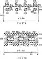
- a number of trenches 304are formed in the silicon substrate 201 to extend in the word line directions in regions for forming word lines later in by using the same technique as used for trench-type DRAM. More specifically, a buffering silicon oxide film 301, silicon nitride film 302 are formed, a resist 303 is formed and patterned thereon, and the silicon substrate 201 is etched by RIE, thereby to make the trenches 304.
- the trenches 304are arrange densely in the word line direction and thinly in the direction orthogonal thereto. Depth of each trench 304 is several times its diameter.
- the substrateis annealed in a hydrogen atmosphere approximately at 1100°C.
- a hydrogen atmosphereapproximately at 1100°C.
- surface migrationoccurs, and due to movements of silicon atoms, openings of the trenches 30-4 are closed, and here is obtained a structure having a plurality of buried voids 305 in which voids are aligned continuously in form of pipes in the direction where the trenches are densely arranged.
- Figs. 33A and 33Bshow the layout of this state and its A-A' cross-section.
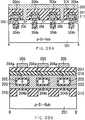
- Fig. 35A, Figs 35B through 39A and 39Bare A-A' cross-sectional views and B-B' cross-sectional views of Fig. 34, respectively.
- the silicon oxide film 310 and the silicon nitride film 311are formed, and a resist 312 is formed and patterned thereon to cover the active layer regions.
- the silicon nitride film 311 and the silicon oxide film 310are etched by RIE, and the silicon substrate 201 is etched as well, thereby to form the device isolating channels 313,
- the device isolating channels 313are formed to be deeper than the voids 305.
- the columnar (convex) active layers 202 in which the voids 305 transversely pass throughare formed in respective transistor forming regions.
- the active layers 202are formed in a grating-shaped continuous pattern similarly to the second embodiment to form each drain diffusion layer to be shared by transistors adjacent in the bit line direction and to form each source diffusion layer to be shared by transistors adjacent in the word line directions.
- the silicon nitride film 311 and the silicon oxide film 310are removed by etching, and another silicon oxide film 315 is formed and processed by etch-back to obtain a structure where the silicon oxide film 315 is buried in the device isolating channels 313 to function as device separating insulation films.
- Surfaces of the silicon oxide films 315are approximately aligned with bottoms of the voids 305 not to close openings of the voids 305 passing through the active layers 202.
- a gate insulating film 203is formed, and a gate electrode 204 made of a polycrystalline silicon film to be used as word lines are formed and patterned along the voids 305.
- the top surface of the gate electrode 204is kept covered by the silicon nitride film 316.
- the gate insulating film 203when formed by thermal oxidation, is formed not only on the top surface of the active layer 202 but also on inner walls of the voids 305.
- the gate electrode 204is buried also in the voids 305.
- gate electrode portions 204a formed on the top surface of the active layer 202 and the gate electrode portions 204b buried in the voids 305are connected at end portions of the voids 305 to extend continuously as word lines.
- transistorsare formed having the top and bottom surfaces and continuous side surfaces of the active layer 202 as their channels.
- This transistor structureis a SGT structure rotated by 90°C from that of the first embodiment.
- a silicon nitride film 317is formed and processed by etch-back by RIE to remain only on side walls of the gate electrode, and source and drain diffusion layers 206 are formed by doping As ions.
- the source and drain diffusion regions 206are formed to be deeper than the top end level of the voids 305. As a result, the bulk region of each transistor can be held floating by electrical isolation by the gate insulating film 203, diffusion layers and device isolating insulation film.
- the inter-layer insulating film 207is formed, contact holes are made in the drain diffusion layer regions, and bit lines 205 are formed to extend orthogonally to the word lines.
- the contactsoverlap the word lines due to misalignment between the bit line contacts and the word lines, since there is the silicon nitride film on the top and side surfaces of the word lines, they behave as a protective film of the contacts during the etching process of the silicon oxide film, and the bit lines and the word lines are prevented from short circuit.
- the word linescan be arranged in minimum pitches.
- the single-transistor memory cell MCexecutes dynamic write/read operations according to the same principle as that of the first embodiment.
- the gate electrodeis formed to encircle the silicon layer and oppose to four surfaces thereof, a large gate capacity can be obtained from a small cell area, and therefore, favorable write and read characteristics are obtained.
- the transistor structures according to the second and third embodimentsare applicable not only to single-transistor DRAM cells but also to, in general, integrated circuits integrating transistors having a large gate capacity with a small area.
- top and bottom portions of the silicon layerare used as channels, it is possible to use only one of them as a channel. For example, a transistor using only the top wall of the void 305 as the channel can be made.
Landscapes
- Semiconductor Memories (AREA)
- Dram (AREA)
- Non-Volatile Memory (AREA)
Abstract
Description
- This invention relates to a dynamic semiconductor memorydevice (DRAM) and its manufacturing method.
- In conventional DRAM, each memory cells is made up of aMOS transistor and a capacitor. Employment of trench capacitorstructures and stacked capacitor structures has greatlyprogressed miniaturization of DRAM. Currently, size of eachmemory cell (cell size) has been reduced to the area of 2Fx4F=8F2where F is the minimum processible size. That is, the minimumprocessible size F has been getting smaller and smaller throughsome periods of generation. If the cell size is generallyexpressed as αF2, the coefficient α has also decreased together,and today with F=0.18µm, α=8 has been realized.
- To continue this trend regarding the cell size or chip size,it is requested to satisfy α<8 for F<18µm and α<6 for F<13µm,together with further progress of micro fabrication, it is animportant issue how small area each cell can be formed in. Inthis connection, there are various proposals toward reducing thecell size of one-transistor/one capacitor memory cells to 6F2 or4F2. However, practical application of these proposals is noteasy because of the problems such as increase of electricalinterference between adjacent memory cells and difficulties inthe manufacturing techniques including processing and formationof films.
- According to an embodiment of the present invention, thereis provided a semiconductor memory device comprising:
- a source diffusion layer formed on a semiconductorsubstrate and connected to a fixed potential line;
- a plurality of columnar semiconductor layers arranged ina matrix form and formed on the source diffusion layer and eachhaving one end connected to the source diffusion layer commonly, the columnar semiconductor layer taking a first data state witha first threshold voltage that excessive majority carriers areaccumulated in the columnar semiconductor layer, and a seconddata state with a second threshold voltage that excessive majoritycarriers are discharged from the columnar semiconductor layer;
- a plurality of drain diffusion layers each formed at theother end of the columnar semiconductor layer;
- a plurality of gate electrodes each opposed to the columnarsemiconductor layer via a gate insulating film, and connectedto the word line;
- a plurality of word lines each connected to correspondingthe gate electrodes; and
- a plurality of bit lines each connected to correspondingthe drain diffusion layers, the bit lines being perpendicularto the word lines.
- Fig. 1 is a diagram that shows a layout of a DRAM cell arrayaccording to an embodiment of the invention;
- Fig. 2 is a cross-sectional view taken along the A-A' lineof Fig. 1;
- Fig. 3 is a cross-sectional view taken along the B-B' lineof Fig. 1;
- Fig. 4 is a equivalent circuit diagram of the same DRAMcell array;
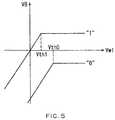
- Fig. 5 is a diagram that shows a relation between a wordline potential and a bulk potential in the same DRAM;
- Fig. 6 is a diagram for explaining a data read system ofthe same DRAM cell;
- Fig. 7 is a diagram for explaining a data read system ofthe same DRAM cell;
- Fig. 8 shows waveforms of read/refresh operations of data"1" by the same DRAM cell;
- Fig. 9 shows waveforms of read/refresh operations data "0"by the same DRAM cell;
- Fig. 10 shows waveforms of read operation of data "0" andwrite operation of data "1" by the same DRAM cell;
- Fig. 11 shows waveforms of read operation of data "1" andwrite operation of data "1" by the same DRAM cell;
- Fig. 12 is a diagram of the same DRAM cell array under itsmanufacturing process;
- Fig. 13 is a diagram of the same DRAM cell array under itsmanufacturing process;
- Fig. 14 is a diagram of the same DRAM cell array under itsmanufacturing process;
- Fig. 15 is a diagram of the same DRAM cell array under itsmanufacturing process;
- Fig. 16 is a diagram of the same DRAM cell array under itsmanufacturing process;
- Fig. 17 is a diagram of the same DRAM cell array under itsmanufacturing process;
- Fig. 18 is a diagram that shows a further substratestructure;
- Fig. 19 is a cross-sectional view of a further DRAM cellarray;
- Fig. 20 is a cross-sectional view of a further DRAM cellarray;
- Fig. 21 is a diagram that shows a memory cell structureaccording to a further embodiment;
- Fig. 22 is a diagram that shows a layout of a DRAM cellarray according to the same embodiment;
- Fig. 23 is a cross-sectional view taken along the B-B' lineof Fig. 22;
- Fig. 24 is a cross-sectional view taken along the A-A' lineof Fig. 22;
- Fig. 25 is a diagram of the same DRAM cell array under itsmanufacturing process;
- Fig. 26 is a diagram of the same DRAM cell array under itsmanufacturing process;
- Fig. 27 is a diagram of the same DRAM cell array under itsmanufacturing process;
- Fig. 28 is a diagram of the same DRAM cell array under itsmanufacturing process;
- Fig. 29 is a diagram of the same DRAM cell array under its manufacturing process;
- Fig. 30 is a perspective of the structure obtained throughthe process of Fig. 28;
- Fig. 31 is a diagram that shows a memory cell structureaccording to a still further embodiment;
- Fig. 32A is a plan view that shows a pretreatment processof a substrate according to the same embodiment;
- Fig. 32B is a cross-sectional view taken along the A-A'line of Fig. 32A;
- Fig. 33A is a plan view that shows a pretreatment processof a substrate according to the same embodiment;
- Fig. 33B is a cross-sectional view taken along the A-A'line of Fig. 33A;
- Fig. 34 is a plan view of a DRAM cell array according tothe same embodiment;
- Fig. 35A is a cross-sectional view taken along the A-A'line of Fig. 34 to show a manufacturing process of the sameembodiment;
- Fig. 35B is a cross-sectional view taken along the A-A'line of Fig. 34 to show a manufacturing process of the sameembodiment;
- Fig. 36A is a cross-sectional view taken along the A-A'line of Fig. 34 to show a manufacturing process of the sameembodiment;
- Fig. 36B is a cross-sectional view taken along the A-A'line of Fig. 34 to show a manufacturing process of the sameembodiment;
- Fig. 37A is a cross-sectional view taken along the A-A'line of Fig. 34 to show a manufacturing process of the sameembodiment;
- Fig. 37B is a cross-sectional view taken along the A-A'line of Fig. 34 to show a manufacturing process of the sameembodiment;
- Fig. 38A is a cross-sectional view taken along the A-A'line of Fig. 34 to show a manufacturing process of the sameembodiment;
- Fig. 38B is a cross-sectional view taken along the A-A' line of Fig. 34 to show a manufacturing process of the sameembodiment;
- Fig. 39A is a cross-sectional view taken along the A-A'line of Fig. 34 to show a manufacturing process of the sameembodiment; and
- Fig. 39B is a cross-sectional view taken along the A-A'line of Fig. 34 to show a manufacturing process of the sameembodiment.
- Embodiments of the invention will now be explained belowwith reference to the drawings.
- Fig. 1 is a diagram that shows a layout of a DRAM cell arrayaccording to an embodiment of the invention, and Figs. 2 and 3are cross-sectional views taken along the A-A' and B-B' linesof Fig. 1, respectively. Columnar silicon layers are formed inpositions of respective memory cells MC by processing a p-
typesilicon substrate 1. Each memory cell MC is composed of a verticalMOS transistor formed by using thecolumnar silicon layer 2. - More specifically, the transistor of each memory cell MCis an NMOS transistor in which a gate electrode is formed tosurround the
columnar silicon layer 2 via agate insulating film 3 and an n+-typesource diffusion layer 6 is formed at the bottom.This transistor structure is disclosed as so-called "SGT" in thepaper "Impact of Surrounding Gate Transistor (SGT) for highdensity LSI's" by H. Takato et al. (IEEE Transactions on ElectronDevices, vol. 38, No. 3, pp. 573-577, March 1991). - It is important for the
source diffusion layer 6 formedat the bottom of thecolumnar silicon layer 2 to lie across thefull extent of the bottom of thecolumnar silicon layer 2 toelectrically insulate the p-type region of thecolumnar siliconlayer 2 from the p-type region of thesubstrate 1. Thereby, ineach memory cell MC, thecolumnar silicon layer 2 is held floatingand can be controlled in bulk potential to enable dynamicrecording operation by one transistor according to the invention,as explained later. In addition, thesource diffusion layer 6 is formed to cover the entire surface of thesubstrate 1 to behaveas a fixed potential line SS common to all memory cells MC. - The
gate electrodes 4 surrounding thecolumnar siliconlayer 2 are formed of a polycrystalline silicon film. Bymaintaining the same polycrystalline silicon film as thegateelectrodes 4 continuously in one direction of the cell array,word lines (WL) 9 commonly connecting thegate electrodes 4 areformed. The surface having formed the transistors is covered byan inter-layerinsulating film 7, andbit lines 8 are formedthereon. The bit lines 8 extend in the direction orthogonal totheword lines 9, and are connected to draindiffusion layers 5 of respective memory cells MC. - In this DRAM cell array, if the
word lines 9 and thebitlines 8 are processed with lines and spaces of the minimumprocessible size F, as shown in Fig. 1, its unit cell area is2Fx2F=4F2. - Fig. 4 shows a equivalent circuit of this DRAM cell array.Each memory cell MC is composed only of a single NMOS transistor.Drains are connected to bit lines BL, gates are connected to wordlines WL and sources are commonly connected to a fixed potentialline SS. In this case, sense amplifiers SA are connected in anopen bit line system, and a pair of bit lines BL, BBL of cellarrays disposed at opposite sides of each sense amplifier areconnected to the sense amplifier SA. Therefore, although notshown, at least one dummy cell is disposed in each of the cellarrays associated with bit lines BL, BBL.
- Operation principle of the DRAM cell mad up of the NMOStransistor utilizes excessive accumulation of holes that aremajority carriers in the bulk region (p-type
columnar siliconlayer 2 insulated and isolated from others) of the MOS transistor.More specifically, a predetermined positive potential is appliedto the gate electrode while a large channel current is suppliedfrom thedrain diffusion layer 5, thereby to generate hot carriersby impact ionization and have thesilicon layer 2 excessivelyhold holes that are majority carriers of thesilicon layer 2.The excessive hold storage state (with a higher potential thanin the thermal equilibrium state) is determined as data "1", for example. The state, in which the pn junction between thedraindiffusion layer 5 and thesilicon layer 2 is forwardly biasedand excessive holes in thesilicon layer 2 are released to thedrain side, is determined as data "0". - Data "0" and "1" are different potentials of the bulk region,and they are stored as a difference of threshold voltages of theMOS transistor. That is, threshold voltage Vth1 in the sate ofhi potential data "1" of the bulk region by storage of holes islower than threshold voltage Vth0 in the state of data "0". Inorder to maintain the data "1" state accumulating majoritycarriers, holes, in the bulk region, it is necessary to applya negative bias voltage to the word line WL. In this data holdingstate, read operation may be done as far as write operation ofthe opposite data (erase) is not effected. That is, unlike aone-transistor/one-capacitor DRAM relying charge storage of acapacitor, non-destructive read-out is possible.
- There are some data read-out systems. Relation betweena word line potential Vwl and a bulk potential VB is as shownin Fig. 5 in the relation between data "0" and "1". Therefore,a first data read-out method supplies the word line WL with aread-out potential that is an intermediate value between thethreshold voltages Vth0 and Vth1 of the data "0" and "1", andutilizes the phenomenon that no current flows in memory cellswith data "0" but a current flows in memory cells with data "1".More specifically, for example, the bit line BL is prechargedto a predetermined potential VBL, and the word line WL is drivenlater. As a result, as shown in Fig. 6, in case of data "0", nochange occurs in the bit line precharge potential VBL, and incase of data "1", the precharge potential VBL decreases.
- A second read-out system supplies the bit line BL with acurrent after activating the word line WL, and utilizes adifference in rising speed of the bit line potential, dependingupon conductivities of "0" and "1". Simply, the bit line BL isprecharged to 0 V, and the word line WL is activated as shownin Fig. 7, thereby to supply the bit line current. At that time,by detecting the difference in rising speed of the potential inthe bit line, data can be distinguished.
- A third read-out system reads a difference between bit linecurrents that are different depending on "0" and "1" when thebit line BL is clamped to a predetermined potential. To read outthe current difference, a current-voltage converting circuit isnecessary. Finally, however, a sense output is issued throughdifferential amplification of the potential difference.
- In the present invention, in order to selectively writedata "0", that is, to ensure that holes are emitted only fromthe bulk region of a memory cell selected by potentials of aselected word line WL and a bit line BL from the memory cell array,capacity coupling between the word line WL and the bulk regionis essential. The state of data "1", with excessive holes storedin the bulk region, has to be maintained in the state where theword line WL is sufficiently biased to the negative direction,and the gate/bulk interstitial capacity of the memory cell becomesequal to the gate oxide film capacity (in which no depletion layeris formed on the surface).
- Additionally, write operation is preferably effected bywriting pulses for both "0" and "1" to save power consumption.Upon writing "0", although a hole current flows from the bulkregion of the selected transistor to the drain and an electroncurrent flows from the drain to the bulk region, it does not occurthat holes are injected to the bulk region.
- More concrete operation waveforms will be explained. Figs.8 through 11 show waveforms of read/refresh and read/writeoperations in case of using the first read-out system configuredto distinguish data depending on the presence or absence ofdischarge to the bit line by the selected cell. Assume that thereference potential given to the fixed potential line SS commonlyconnecting the sources of all memory cells MC is o V.
- Figs. 8 and 9 are waveforms of read/refresh operations ofdata "1" and data "0", respectively. Up to the time t1, the memoryis in the data holding state (non-selected state), and the wordline WL is supplied with a negative potential. At the time t1,the word line WL is raised to a predetermined positive potential.At that time, the word line potential is adjusted to a valuebetween the threshold values Vth0 and Vth1 of data "0" and "1". As a result, in case of data "1", the precharged bit line VBLis becomes a low potential due to a discharge. In case of data"0", the bit line potential VBL is maintained. Thereby, data "1"and "0" are distinguished.
- At the time t2, potential of the word line WL is furtherraised, and at the same time, a positive potential is appliedto the bit line BL (Fig. 8) when the read-out data is "1" whereasa negative potential is applied to the bit line BL (Fig. 9) whenthe read-out data is "0". As a result, if the data of the selectedmemory cell is "1", a large channel current flows and causes impactionization, and excessive holes flow into the bulk region andhave the memory write data "1" again. In case of data "0", thedrain junction is forwardly biased, and holes are emitted fromthe bulk region and have the memory write data "0" again.
- At the time t3, the word line WL is negatively biased,thereby to complete the read/refresh operations. In the othernon-selected memory cells connected to the bit line BL commonlywith the memory cell from which data "1" has been read out, sincethe word lines WL are held in negative potentials, that is, thebulk region is held in a negative potential, no channel currentflows, and writing does not occur. Also in the other non-selectedmemory cells connected to the bit line BL commonly to the memorycell from which data "0" has been read out, the word line WL areheld in negative potentials, and emission of holes does not occur.
- Figs. 10 and 11 are waveforms of read/write operations ofdata "1" and data "0" by the same read-out system. Read-outoperations at the time t1 in Figs. 10 and 11 are the same as thoseof Figs. 8 and 9, respectively. After reading, at the time t2,the word line WL is raised to a high potential, and in case ofwriting data "0" in the same selected cell, a negative potentialis simultaneously applied to the bit line BL (Fig. 10). In caseof writing data "1", a positive potential is applied to the bitline BL (Fig. 11). As a result, in the cell to which the data"0" is given, the drain junction is forwardly biased, and holesin the bulk region are emitted. In the cell to which the data"1" is given, a channel current flows, impact ionization occurs,and holes are accumulated in the bulk region.
- As explained above, the DRAM cell according to theinvention is made of SGT having the floating bulk regionelectrically isolated from others, and enables realization ofthe cell size of 4F2. In addition, potential control of thefloating bulk region is attained by using the capacity couplingfrom the gate electrode, without using back gate control, andthe source diffusion layer is fixed in potential as well. Thatis, control of read/write operations is easily accomplished onlyby the word line WL and the bit line BL. furthermore, since thememory cell is basically can be read in a non-destructive mode,it is not necessary to provide the sense amplifier for each bitline, and layout of the sense amplifiers is easy. Moreover,because of the current read-out system, it has a resistance tonoise, and reading is possible even in the open bit line system.
- In addition, by utilizing SGT using the columnarsilicon layer as the memory cell, a lot of effects are obtained.In the memory cell based on the operation principle accordingto the invention as explained above, it is desirable that thebulk potential changes faithfully following to the word line (gateelectrode). Thereby, charges accumulated in the bulk region canbe held without turning on the pn junction. In normal horizontalMOS transistors, capacity between the gate electrode, i.e. theword line, and the bulk region becomes smaller as the transistoris miniaturized, and the capacity of the source and drain pnjunction cannot be disregarded.
- In contrast, when the SGT structure is used, since thechannel region surrounds the columnar silicon layer and thechannel length is determined by the height of the columnar siliconlayer, a large channel length can be obtained independently fromthe horizontal size determined by lithography. In other words,without increasing the horizontal area, a large channel lengthcan be realized within substantially the same area as the bitline contact. Therefore, capacity coupling between the word lineand the bulk region can be increased, and reliable operationcontrol by controlling the bulk potential from the word line isensured.
- Further, in the memory cell according to the invention, it is desirable that the threshold value change largely relativeto changes of the bulk potential. This can be also realized easilyby employing the SGT structure. That is, by producing aconcentration profile in the substrate in its thickness directionsuch that the substrate impurity concentration is high in acentral portion of the channel and the channel concentration nearthe pn junction is low, changes of the threshold value relativeto changes of the bulk potential can be enlarged by the substratebiasing effect while minimizing the junction leakage.furthermore, by reducing the top area of the columnar siliconlayer for contact with the bit line, the pn junction capacityconnected to the bit line can be reduced, and this also contributesto relatively increasing the capacity coupling ratio of the wordline and the bulk region. Further, as a result, since the bitline capacity also decreases, the charge and discharge currentof the bit line capacity upon read and write operations isdiminished, and higher speed and lower power consumption areattained thereby.
- A concrete manufacturing process of the cell arrayexplained with reference to Figs. 1 through 3 is next explainedwith reference to Figs. 12 through 17 that are cross-sectionalviews corresponding to the cross-sectional view of Fig. 2, showingdifferent steps of the manufacturing process.
- As shown in Fig. 12, after a buffering
silicon oxide film 11 is formed to a thickness around 10 nm on a p-type siliconsubstrate 1, asilicon nitride film 12, approximately 200 nm thick,is formed thereon, and a resist 13 is formed and patterned thereonby lithography. - After that, as shown in Fig. 13, using the resist 13 asa mask, the
silicon nitride film 12 and thesilicon oxide film 11 are etched, and thesilicon substrate 1 is further etched tomakechannels 14 extending in crossing directions and therebyform the columnar silicon layers 2. After than, the resist 13and thesilicon nitride film 12 are removed, As ions are implanted,and as shown in Fig. 14, diffusion layers 6, 5 to be used as sourcesand drains, respectively, are formed on tops of thechannels 14and the columnar silicon layers 2. - Thereafter, as shown in Fig. 15, a
gate oxide film 3 isformed on and around thecolumnar silicon layers 2, by thermaloxidation, and apolycrystalline silicon film 40 for forming gateelectrodes is formed subsequently. Through the thermaloxidation process including gate oxidation and subsequentthermal process, the n+-type source diffusion layers 6 formed atbottoms of thechannels 14 diffuse laterally. As a result, p-typeregions of thecolumnar silicon layers 2 and p-type regions ofthesubstrate 1 are electrically isolated by thesource diffusionlayer 6. - After that, the entire surface of the
polycrystallinesilicon film 40 is etched by RIE to form thegate electrodes 4only on side walls of thecolumnar silicon layers 2 as shown inFig. 16, In this etching process, however, spaces between thecolumnar silicon layers 2 aligned in the direction orthogonalto the sheet of Fig. 16 are covered with a resist. As a result,as shown in figs. 1 and 3,word lines 9 are made of the samepolycrystalline silicon film 40 to connect thegate electrodes 4. - After that, a silicon oxide film is formed as shown in Fig.17, and it is leveled by CMP to form the inter-layer
insulatingfilm 7. Subsequently, after contact holes are formed atpositions of thecolumnar silicon layers 2, an Al film is formedand patterned to formbit lines 8, as shown in Fig. 2. Usableas thebit lines 8 are other metal films of W, etc., for example,instead of the Al film, or films of other conductive materials,such as or polycrystalline silicon. Thereafter, although notshown, an inter-layer insulating film is formed to make wiringsfor connection to peripheral circuits. Thesource diffusionlayer 6 formed at bottoms of the columnar silicon layers 2 isconnected to a signal line fixed in potential, such as a groundedline, at a peripheral portion of the cell array. - Through the manufacturing processes explained above, acell array composed of single-transistor memory cells having theSGT structure using a small cell area and ensuring a large gatecapacity can be obtained.
- In the example explained above, the
columnar silicon layers 2 are completely isolated electrically from the substrate by usinglateral diffusion of thesource diffusion layer 6. This is easywhen the diameter of eachcolumnar silicon layer 2 is sufficientlysmall, but it is not always easy when the diameter is relativelylarge. In that case, it is desirable that an n+-type layer tobe used as thesource diffusion layer 6 is built in the substratebeforehand. That is, a structure as shown in Fig. 18 is previouslyprepared as thesilicon substrate 1. - This structure can be obtained, for example, by using ap-
type layer 20 as the substrate, then forming an n+-type buriedlayer 21 on the entire surface of the p-type layer 20, and nextepitaxially growing a p-type silicon layer 22. Alternatively,the substrate of Fig. 18 can be made by preparing independentsilicon substrates as the p-type layers type layer 21 on one of them, and thereafter bonding themdirectly. Using such an epitaxial substrate or a bondedsubstrate, once the columnar silicon layers are formed by etchingthe substrate to the depth of the n+-type layer 21, reliableelectric isolation between the columnar silicon layers and thesubstrate is ensured. - It is not indispensable that bottoms of the columnarsilicon layers are completely closed by the n+-
type layer 6. Forexample, as shown in Fig. 19, even when the n+-type layers 6extending from bottoms of the channels do not completely traversethecolumnar silicon layers 2, only if the depletion layers 23extending from portions encircling thecolumnar silicon layers 2 toward their centers connect to each other under zero bias,p-type regions of thecolumnar silicon layers 2 and p-type regionsof thesubstrate 1 are electrically isolated. - Fig. 20 shows a cross section of another cell arraystructure, which corresponds to Fig. 2. In this example, topportions of the
columnar silicon layers 2 are tapered to diminishthe diameter toward the tops. In this manner, contact area ofeachdrain diffusion layers 5 formed on top ends of thecolumnarsilicon layers 2 with thebit line 8 can be reduced. - In the examples explained heretofore, junction between then*-
type source region 6 and thedrain diffusion layers 5 with the p-type silicon layer 2 is preferably graded junction in whichthe n+-type layer joins the p-type layer via an n-type layergradually decreased in concentration, instead of step-likejunction. In this manner, junction leakage can be reduced, andthe junction capacity can be reduced as well. Even when thisjunction structure is used, since the height of the columnarsilicon layers ensure the channel length, unlike the horizontaltransistors, a sufficiently high p-type impurity concentrationcan be ensured in the central portions of the channels. Therefore,it is convenient for dynamic recording operation by bulk potentialcontrol using the gate capacity. - The first embodiment has been explained above as using asmemory cells MC the transistors having the SGT structure in whichside wall surfaces of the columnar silicon layers are used aschannel regions. In contrast, although using a single transistorin form of a columnar silicon layer as each memory cell MC, thesecond embodiment has the transistor shown in Fig. 21. That is,a
columnar silicon layer 102 formed on asilicon substrate 101is used as an active layer, agate electrode 104 is provided tolie across thecolumnar silicon layer 102 and oppose to the topsurface and opposite side surfaces of thecolumnar silicon layer 102 via agate insulating film 103, and drain and source diffusionlayers are formed at opposite sides of thegate electrode 104.thecolumnar silicon layer 102 is held floating by an insulatingfilm buried at the bottom thereof. - Fig. 22 shows a layout of a DRAM cell according to theinstant embodiment, and Figs. 23 and 24 are cross-sectional viewstaken along the A-A' and B-B' lines of Fig. 22. As explained later,used as the
columnar silicon layer 102 is a p-type silicon layerepitaxially grown on thesilicon substrate 101.Active layer 102,which are convex silicon layers obtained by processing the p-typesilicon layer, are arranged in a pattern of a grating such thateach drain diffusion layer is shared byactive layers 102 ofdifferent memory cells MC adjacent to each other in the bit linedirection and the source diffusion layer is continuously formed in the word line direction as a common source line. - At the bottom of each
active layer 102, asilicon oxidefilm 110 is buried. Asilicon oxide film 111 is buried also ineach device isolating region. Then, thegate electrode 104 isformed as a word line that lies across theactive layer 102 andopposes to its three surfaces. the n+-type source and draindiffusion layer 105 are formed in self alignment with thegateelectrode 104. The surface having formed the transistors iscovered with an inter-layerinsulating film 106, and bitlines 107 are formed thereon. - In this manner, operation principle of the DRAM cell arrayusing a single NMOS transistor as each memory cell MC is the sameas that of the foregoing first embodiment. As already explainedwith the first embodiment, magnitude of the capacity couplingfrom the gate electrode to the floating bulk region is importantfor data write/read operations. Also in this embodiment, sincethe
gate electrode 104 is opposed to three surfaces of theactivelayer 102 made of the columnar silicon layer, a large couplingcapacity is obtained, and a favorable property is obtained. - A manufacturing process for obtaining the cell arraystructure according to the second embodiment is next explainedwith reference to Fig. 25 et seq., which show the cross sectioncorresponding to the cross section shown in Fig. 23. As shownin Fig. 25, the
silicon oxide film 110 is formed on locationsofsilicon substrate 101 where silicon layers should be formedlater as active regions having a grating pattern, with a certaintolerance for misalignment. Thereafter, as shown in Fig. 26, ap-type silicon layer 1020 is epitaxially grown on thesiliconsubstrate 101. - Next as shown in Fig. 27, a buffering
silicon oxide film 120 and asilicon oxide film 121 are formed on thesilicon layer 1020, and a resist 123 is formed and patterned thereon to coverthe regions to be used as active regions by lithography. By RIEusing this resistpattern 123, thesilicon nitride film 121,silicon oxide film 121 andsilicon layer 1020 are etchedsequentially. Consecutively, thesilicon oxide film 110 isetched and the exposedsilicon substrate 101 is also etched to a predetermined depth. - As a result, the
active layer 102 having a convex gratingpattern of the p-type silicon layer 1020, which is the epitaxiallygrown layer, is obtained. At the bottom thereof, thesiliconoxide film 110 is buried. Thereafter, by forming thesiliconoxide film 111, leveling it by CMP, and processing it by etch-backusing RIE, the configuration where thesilicon oxide film 111is buried approximately up to the surface level of thesiliconoxide film 110 is obtained as shown in Fig. 28. Thesilicon oxidefilm 111 is used as the device isolating insulation film forisolating respective transistors in their lateral direction. - The configuration shown in Fig. 28 is illustrated in aperspective view in Fig. 30. The p-type
active layer 102 is shapedinto a grating pattern, and the device isolating insulation filmis buried in spaces. Subsequently, as shown in Fig. 29, afterthegate insulating film 103 is formed on surfaces of the p-typeactive layer 102 (three surfaces including the top surfaceand opposite side surfaces), a polycrystalline silicon film isformed and patterned to form thegate electrodes 104 which willbecome the word lines. - After that, as shown in Fig. 24, using the
gate electrodes 104 as a mask, As ions are injected to form the source and draindiffusion layers 105. These diffusion layers 105 herein has adepth enough to reach the buriedsilicon oxide film 110 as shownin Fig. 24. As a result, the p-type bulk region of the transistorscan be held floating to be independently controlled in potential.Thereafter, the inter-layerinsulating film 106 is formed,contact holes are formed in locations thereof corresponding tothe drain diffusion layers, and bitlines 107 are formed tointersect with the word lines. - Fig. 31 shows an embodiment using still another transistorstructure to make up memory cells MC. On top, bottom and oppositeside surfaces of an
active layer 202 formed on asilicon substrate 201, agate insulating film 203 is formed, and agate electrode 204 is formed to lie across theactive layer 202 and oppose to the top, bottom and opposite side surfaces of theactive layer 202. At opposite sides of thegate electrode 204, source and draindiffusion layers are formed. Fig. 31 illustrates theactivelayer 202 as floating from thesubstrate 201. Actually, however,this structure is made by using a technique of making holes insidea silicon substrate as explained later, and theactive layer 202is not floating. - Here again, the DRAM cell array is made by using a singleNMOS transistor as each memory cell MC, write and read operationsof data are effected in the same manner as the first and secondembodiments. Also in this case, as already explained withreference to the first embodiment, magnitude of the capacitycoupling from the gate electrode to the floating bulk region isimportant for data write/read operations. Since the
gateelectrode 204 is opposed to the top and bottom surfaces of theactive layer 202 mad of the columnar silicon layer, a largecoupling capacity is obtained, and a favorable property isobtained. - A manufacturing method of the DRAM cell array accordingto the third embodiment is explained below in greater detail withreference to Fig. 32A et seq. First, pipe-shaped voids are formedin the
silicon substrate 201. for this purpose, as shown in Fig.32A and its A-A' cross-sectional view, Fig. 32B, a number oftrenches 304 are formed in thesilicon substrate 201 to extendin the word line directions in regions for forming word lineslater in by using the same technique as used for trench-type DRAM.More specifically, a bufferingsilicon oxide film 301,siliconnitride film 302 are formed, a resist 303 is formed and patternedthereon, and thesilicon substrate 201 is etched by RIE, therebyto make thetrenches 304. Thetrenches 304 are arrange denselyin the word line direction and thinly in the direction orthogonalthereto. Depth of eachtrench 304 is several times its diameter. - Then, after the resist 303 is removed and the
siliconnitride film 302 and thesilicon oxide film 301 are removed aswell, the substrate is annealed in a hydrogen atmosphereapproximately at 1100°C. In this process, surface migrationoccurs, and due to movements of silicon atoms, openings of the trenches 30-4 are closed, and here is obtained a structure havinga plurality of buriedvoids 305 in which voids are alignedcontinuously in form of pipes in the direction where the trenchesare densely arranged. Figs. 33A and 33B show the layout of thisstate and its A-A' cross-section. - The technique making pipe-shaped voids inside the siliconsubstrate in this manner is taught in detail in the paper disclosedby T. Sato et al, "A New Substrate Engineering for Formation EmptySpace in Silicon (ESS) Induced by Silicon Surface Migration" (IEDM'99, Technical Digest, pp. 517-520).
- In this manner, using the
silicon substrate 201 havingburiedvoids 304, as shown in Fig. 34, active regions partitionedin a grating form by thedevice isolating region 306 are formedto obtain a cell array having the word lines 204 overlapping thevoids 305 and thebit lines 204 extending orthogonally thereto.More specifically, a part of the manufacturing process from thedevice isolating process to the device forming process isexplained below with reference to Fig. 35A, Figs 35B through 39Aand 39B which are A-A' cross-sectional views and B-B' cross-sectionalviews of Fig. 34, respectively. - First referring to Figs. 35A and 35B, the
silicon oxidefilm 310 and thesilicon nitride film 311 are formed, and a resist312 is formed and patterned thereon to cover the active layerregions. Then, thesilicon nitride film 311 and thesilicon oxidefilm 310 are etched by RIE, and thesilicon substrate 201 is etchedas well, thereby to form thedevice isolating channels 313, Thedevice isolating channels 313 are formed to be deeper than thevoids 305. As a result, the columnar (convex)active layers 202in which thevoids 305 transversely pass through are formed inrespective transistor forming regions. Actually, theactivelayers 202 are formed in a grating-shaped continuous patternsimilarly to the second embodiment to form each drain diffusionlayer to be shared by transistors adjacent in the bit linedirection and to form each source diffusion layer to be sharedby transistors adjacent in the word line directions. - After that, as shown in Figs. 36A and 36B, the
siliconnitride film 311 and thesilicon oxide film 310 are removed by etching, and anothersilicon oxide film 315 is formed andprocessed by etch-back to obtain a structure where thesiliconoxide film 315 is buried in thedevice isolating channels 313to function as device separating insulation films. Surfaces ofthesilicon oxide films 315 are approximately aligned with bottomsof thevoids 305 not to close openings of thevoids 305 passingthrough theactive layers 202. - After that, as shown in Figs. 37A and 37B, a
gate insulatingfilm 203 is formed, and agate electrode 204 made of apolycrystalline silicon film to be used as word lines are formedand patterned along thevoids 305. The top surface of thegateelectrode 204 is kept covered by thesilicon nitride film 316.Thegate insulating film 203, when formed by thermal oxidation,is formed not only on the top surface of theactive layer 202but also on inner walls of thevoids 305. Thegate electrode 204is buried also in thevoids 305. that is,gate electrode portions 204a formed on the top surface of theactive layer 202 and thegate electrode portions 204b buried in thevoids 305 are connectedat end portions of thevoids 305 to extend continuously as wordlines. In other words, transistors are formed having the top andbottom surfaces and continuous side surfaces of theactive layer 202 as their channels. This transistor structure is a SGTstructure rotated by 90°C from that of the first embodiment. - After that, as shown in figs. 38A and 38B, a
silicon nitridefilm 317 is formed and processed by etch-back by RIE to remainonly on side walls of the gate electrode, and source and draindiffusion layers 206 are formed by doping As ions. The sourceand draindiffusion regions 206 are formed to be deeper than thetop end level of thevoids 305. As a result, the bulk region ofeach transistor can be held floating by electrical isolation bythegate insulating film 203, diffusion layers and deviceisolating insulation film. - After that, as shown in Figs. 39A and 39B, the inter-layer
insulating film 207 is formed, contact holes are made in the draindiffusion layer regions, and bitlines 205 are formed to extendorthogonally to the word lines. In this case, even if the contactsoverlap the word lines due to misalignment between the bit line contacts and the word lines, since there is the silicon nitridefilm on the top and side surfaces of the word lines, they behaveas a protective film of the contacts during the etching processof the silicon oxide film, and the bit lines and the word linesare prevented from short circuit. As a result, the word linescan be arranged in minimum pitches. - The single-transistor memory cell MC according to theinstant invention executes dynamic write/read operationsaccording to the same principle as that of the first embodiment.Similarly to the SGT structure, since the gate electrode is formedto encircle the silicon layer and oppose to four surfaces thereof,a large gate capacity can be obtained from a small cell area,and therefore, favorable write and read characteristics areobtained.
- The transistor structures according to the second and thirdembodiments are applicable not only to single-transistor DRAMcells but also to, in general, integrated circuits integratingtransistors having a large gate capacity with a small area. Incase of the third embodiment, top and bottom portions of thesilicon layer are used as channels, it is possible to use onlyone of them as a channel. For example, a transistor using onlythe top wall of the void 305 as the channel can be made.
- As described above, according to the invention, it ispossible to provide a semiconductor memory device capable ofdynamic recording of binary data with fewer signal lines by usingsingle-transistor memory cells having a gate large capacity witha small cell area.
Claims (15)
- A semiconductor memory device comprising:a source diffusion layer formed on a semiconductorsubstrate and connected to a fixed potential line;a plurality of columnar semiconductor layers arranged ina matrix form and formed on said source diffusion layer and eachhaving one end connected to said source diffusion layer commonly,said columnar semiconductor layer taking a first data state witha first threshold voltage that excessive majority carriers areaccumulated in said columnar semiconductor layer, and a seconddata state with a second threshold voltage that excessive majoritycarriers are discharged from said columnar semiconductor layer;a plurality of drain diffusion layers each formed at theother end of said columnar semiconductor layer;a plurality of gate electrodes each opposed to saidcolumnar semiconductor layer via a gate insulating film, andconnected to said word line;a plurality of word lines each connected to correspondingsaid gate electrodes; anda plurality of bit lines each connected to correspondingsaid drain diffusion layers, said bit lines being perpendicularto said word lines.
- The semiconductor memory device according to claim 1wherein said source diffusion layer is made as a planar shapeand commonly connects said columnar semiconductor layersarranged along said bit lines and said word lines.
- The semiconductor memory device according to claim 1wherein said source diffusion layer is formed to commonly connectsaid columnar semiconductor layers aligned along each said bitline.
- The semiconductor memory device according to claim 1wherein said source diffusion layer is formed to commonly connectsaid columnar semiconductor layers aligned along each said word line.
- The semiconductor memory device according to claim 1wherein each said columnar semiconductor layer is formed byprocessing said semiconductor substrate, and said sourcediffusion layer is formed at the bottom portions of said columnarsemiconductor layers to keep said columnar semiconductor layersfloating state where said columnar semiconductor layers areelectrically isolated from said semiconductor substrate.
- The semiconductor memory device according to claim 1wherein said first data state is set by holding in said columnarsemiconductor layer supplied with a predetermined potential fromsaid gate electrode an excessive amount of majority carriersgenerated by impact ionization caused by flowing a channel currentfrom said drain diffusion layer to said columnar semiconductorlayer, and said second data state is set by discharging excessivemajority carriers in said columnar semiconductor layer suppliedwith a predetermined potential from said gate electrode to saiddrain diffusion layer by applying a forward bias between saiddrain diffusion layer and said columnar semiconductor layer.
- The semiconductor memory device according to claim 1wherein said semiconductor substrate is a p-type siliconsubstrate.
- The semiconductor memory device according to claim 1wherein, upon a date write operation, said fixed potential lineis set at a reference potential and wherein a first potentialhigher than said reference potential is applied to a selectedword line, a second potential lower than said reference potentialis applied to non-selected word lines, and a third potentialhigher than said reference potential and a fourth potential lowerthan said reference potential are applied to said bit linesdepending upon said first and second data states, respectively.
- The semiconductor memory device according to claim 8 wherein, upon a data read operation, a fifth potential betweensaid first threshold voltage and said second threshold voltageand higher than said reference potential is applied to a selectedword line, to detect whether a selected memory cell is in aconduction state or in a non-conduction state.
- The semiconductor memory device according to claim8 wherein, upon a data read operation, a fifth potential higherthan said first and second threshold voltages and higher thansaid reference potential is applied to a selected word line, todetect conductivity of a selected memory cell.
- A semiconductor memory device comprising:a plurality of columnar semiconductor layers formed on asemiconductor substrate via an insulating film, and each takinga first data state with a first threshold voltage that excessivemajority carriers are accumulated in said columnar semiconductorlayer, and a second data state with a second threshold voltagethat excessive majority carriers are discharged from saidcolumnar semiconductor layer;a plurality of source diffusion layers each formed atone-side ends of said columnar semiconductor layer and connectedto a fixed potential line;a plurality of drain diffusion layers each formed at theother ends of said columnar semiconductor layer;a plurality of gate electrodes each opposed to saidcolumnar semiconductor layer via a gate insulating film, andconnected to said word line;.a plurality of word lines each connected to correspondingsaid gate electrodes; anda plurality of bit lines each connected to correspondingsaid drain diffusion layers, said bit lines being perpendicularto said word lines.
- A semiconductor memory device comprising:a plurality of columnar semiconductor layers each formedon a semiconductor substrate and extended in one direction;a plurality of gate electrodes each including a firstportion and a second portion, said first and second portionsextending in other direction perpendicular to said one direction,said first and second portions being formed to cross said columnarsemiconductor layer and sandwich said columnar semiconductorlayer from the top and the bottom thereof via an insulating film,said first and second portions being connected to each other atend portions thereof;a plurality of source diffusion layers and a draindiffusion layers each source diffusion layer and each draindiffusion layer being formed at both sides of each said columnarsemiconductor layer, each said source layer and each said drainlayer being positioned at both sides of said electrode;a plurality of word lines each connected to correspondingsaid gate electrodes; anda plurality of bit lines each connected to correspondingsaid drain diffusion layers, said bit lines being perpendicularto said word lines.
- A semiconductor integrated circuit device having atransistor integrated on a semiconductor substrate, saidtransistor comprising:a columnar semiconductor layer formed on saidsemiconductor substrate to extend in one direction;a gate electrode including a first portion and a secondportion, said first and second portions extending in otherdirection perpendicular to said one direction, said first andsecond portions being formed to cross said columnar semiconductorlayer and sandwich said columnar semiconductor layer via aninsulating film, said first and second portions being connectedto each other at end portions thereof; anda source diffusion layer and a drain diffusion layer ofsaid columnar semiconductor layer, said source and draindiffusion layers being positioned at both sides of said electrode.
- A manufacturing method of a semiconductor memory devicehaving a first data state with a first threshold voltage that excessive majority carriers are accumulated in said columnarsemiconductor layer, and a second data state with a secondthreshold voltage that excessive majority carriers aredischarged from said columnar semiconductor layer, comprising:forming an musk pattern on a semiconductor substrate tocover a portions where columnar semiconductor layer will beformed;etching said semiconductor layer to form said columnarsemiconductor layers;burying device isolating insulation films at bottomportions of device isolating channels;deffusing one conductive type impurities into said bottomportions of said channels and top portions of said columnarsemiconductor layers, to form source and drain diffusion layers;forming gate insulating layers on top surfaces and sidesurfaces of said columnar semiconductor layers; andforming gate electrodes on said gate insulating layers.
- A manufacturing method of a semiconductor memorydevice having a first data state with a first threshold voltagethat excessive majority carriers are accumulated in said columnarsemiconductor layer, and a second data state with a secondthreshold voltage that excessive majority carriers aredischarged from said columnar semiconductor layer, comprising:forming trenches in a semiconductor substrate in a densealignment in a first direction and in a thin alignment in a seconddirection perpendicular to said first direction;annealing said semiconductor substrate to cause surfacemigration and thereby close upper openings of said trenches toform voids buried in said semiconductor substrate and extendingin said one direction, from corresponding said closed trenches;forming a device isolating channels deeper than said voidsin a device isolating regions of said semiconductor substrateto form active layers each having said void passing through abottom portion thereof;burying said device isolating grooves with deviceisolating layers to a depth not closing both ends of said voids;forming gate insulating films each including a firstinsulating film on surface of said active layer and secondinsulating film on the inner wall surface of said void;forming gate electrodes such that each said gate electrodeincludes a first portion and a second portion, said first andsecond portions extending in other direction perpendicular tosaid one direction, said first and second portions being formedto cross said active layer, said first portion being on said firstinsulating film and said second portion being on said secondinsulating film, said first and second portions being connectedto each other at end portions thereof; andforming source and drain diffusion layers in said activelayer in self alignment with said gate electrode.
Applications Claiming Priority (2)
| Application Number | Priority Date | Filing Date | Title |
|---|---|---|---|
| JP2000274221 | 2000-09-08 | ||
| JP2000274221AJP4064607B2 (en) | 2000-09-08 | 2000-09-08 | Semiconductor memory device |
Publications (2)
| Publication Number | Publication Date |
|---|---|
| EP1191596A2true EP1191596A2 (en) | 2002-03-27 |
| EP1191596A3 EP1191596A3 (en) | 2008-10-08 |
Family
ID=18760014
Family Applications (1)
| Application Number | Title | Priority Date | Filing Date |
|---|---|---|---|
| EP01120769AWithdrawnEP1191596A3 (en) | 2000-09-08 | 2001-09-07 | Semiconductor memory device and its manufacturing method |
Country Status (6)
| Country | Link |
|---|---|
| US (1) | US6891225B2 (en) |
| EP (1) | EP1191596A3 (en) |
| JP (1) | JP4064607B2 (en) |
| KR (1) | KR100419269B1 (en) |
| CN (1) | CN1199280C (en) |
| TW (1) | TW511279B (en) |
Cited By (58)
| Publication number | Priority date | Publication date | Assignee | Title |
|---|---|---|---|---|
| US6873539B1 (en) | 2001-06-18 | 2005-03-29 | Pierre Fazan | Semiconductor device |
| US6912150B2 (en) | 2003-05-13 | 2005-06-28 | Lionel Portman | Reference current generator, and method of programming, adjusting and/or operating same |
| US7061050B2 (en) | 2002-04-18 | 2006-06-13 | Innovative Silicon S.A. | Semiconductor device utilizing both fully and partially depleted devices |
| US7085156B2 (en) | 2003-05-13 | 2006-08-01 | Innovative Silicon S.A. | Semiconductor memory device and method of operating same |
| US7085153B2 (en) | 2003-05-13 | 2006-08-01 | Innovative Silicon S.A. | Semiconductor memory cell, array, architecture and device, and method of operating same |
| US7170807B2 (en) | 2002-04-18 | 2007-01-30 | Innovative Silicon S.A. | Data storage device and refreshing method for use with such device |
| US7177175B2 (en) | 2003-09-24 | 2007-02-13 | Innovative Silicon S.A. | Low power programming technique for a floating body memory transistor, memory cell, and memory array |
| US7251164B2 (en) | 2004-11-10 | 2007-07-31 | Innovative Silicon S.A. | Circuitry for and method of improving statistical distribution of integrated circuits |
| US7301838B2 (en) | 2004-12-13 | 2007-11-27 | Innovative Silicon S.A. | Sense amplifier circuitry and architecture to write data into and/or read from memory cells |
| US7301803B2 (en) | 2004-12-22 | 2007-11-27 | Innovative Silicon S.A. | Bipolar reading technique for a memory cell having an electrically floating body transistor |
| US7335934B2 (en) | 2003-07-22 | 2008-02-26 | Innovative Silicon S.A. | Integrated circuit device, and method of fabricating same |
| US7355916B2 (en) | 2005-09-19 | 2008-04-08 | Innovative Silicon S.A. | Method and circuitry to generate a reference current for reading a memory cell, and device implementing same |
| WO2008042165A3 (en)* | 2006-09-29 | 2008-05-29 | Micron Technology Inc | Transistor surround gate structure with partial silicon-on-insulator for memory cells, memory arrays, memory devices and systems and methods of forming same |
| US7436069B2 (en)* | 2004-12-02 | 2008-10-14 | Nec Electronics Corporation | Semiconductor device, having a through electrode semiconductor module employing thereof and method for manufacturing semiconductor device having a through electrode |
| US7476939B2 (en) | 2004-11-04 | 2009-01-13 | Innovative Silicon Isi Sa | Memory cell having an electrically floating body transistor and programming technique therefor |
| US7492632B2 (en) | 2006-04-07 | 2009-02-17 | Innovative Silicon Isi Sa | Memory array having a programmable word length, and method of operating same |
| US7542340B2 (en) | 2006-07-11 | 2009-06-02 | Innovative Silicon Isi Sa | Integrated circuit including memory array having a segmented bit line architecture and method of controlling and/or operating same |
| US7542345B2 (en) | 2006-02-16 | 2009-06-02 | Innovative Silicon Isi Sa | Multi-bit memory cell having electrically floating body transistor, and method of programming and reading same |
| US7606066B2 (en) | 2005-09-07 | 2009-10-20 | Innovative Silicon Isi Sa | Memory cell and memory cell array having an electrically floating body transistor, and methods of operating same |
| US7606098B2 (en) | 2006-04-18 | 2009-10-20 | Innovative Silicon Isi Sa | Semiconductor memory array architecture with grouped memory cells, and method of controlling same |
| US7683430B2 (en) | 2005-12-19 | 2010-03-23 | Innovative Silicon Isi Sa | Electrically floating body memory cell and array, and method of operating or controlling same |
| US7924630B2 (en) | 2008-10-15 | 2011-04-12 | Micron Technology, Inc. | Techniques for simultaneously driving a plurality of source lines |
| US7933140B2 (en) | 2008-10-02 | 2011-04-26 | Micron Technology, Inc. | Techniques for reducing a voltage swing |
| US7933142B2 (en) | 2006-05-02 | 2011-04-26 | Micron Technology, Inc. | Semiconductor memory cell and array using punch-through to program and read same |
| US7947543B2 (en) | 2008-09-25 | 2011-05-24 | Micron Technology, Inc. | Recessed gate silicon-on-insulator floating body device with self-aligned lateral isolation |
| US7957206B2 (en) | 2008-04-04 | 2011-06-07 | Micron Technology, Inc. | Read circuitry for an integrated circuit having memory cells and/or a memory cell array, and method of operating same |
| US8014195B2 (en) | 2008-02-06 | 2011-09-06 | Micron Technology, Inc. | Single transistor memory cell |
| US8064274B2 (en) | 2007-05-30 | 2011-11-22 | Micron Technology, Inc. | Integrated circuit having voltage generation circuitry for memory cell array, and method of operating and/or controlling same |
| US8069377B2 (en) | 2006-06-26 | 2011-11-29 | Micron Technology, Inc. | Integrated circuit having memory array including ECC and column redundancy and method of operating the same |
| US8085594B2 (en) | 2007-06-01 | 2011-12-27 | Micron Technology, Inc. | Reading technique for memory cell with electrically floating body transistor |
| US8139418B2 (en) | 2009-04-27 | 2012-03-20 | Micron Technology, Inc. | Techniques for controlling a direct injection semiconductor memory device |
| US8174881B2 (en) | 2009-11-24 | 2012-05-08 | Micron Technology, Inc. | Techniques for reducing disturbance in a semiconductor device |
| US8189376B2 (en) | 2008-02-08 | 2012-05-29 | Micron Technology, Inc. | Integrated circuit having memory cells including gate material having high work function, and method of manufacturing same |
| US8194487B2 (en) | 2007-09-17 | 2012-06-05 | Micron Technology, Inc. | Refreshing data of memory cells with electrically floating body transistors |
| US8199595B2 (en) | 2009-09-04 | 2012-06-12 | Micron Technology, Inc. | Techniques for sensing a semiconductor memory device |
| US8213226B2 (en) | 2008-12-05 | 2012-07-03 | Micron Technology, Inc. | Vertical transistor memory cell and array |
| US8223574B2 (en) | 2008-11-05 | 2012-07-17 | Micron Technology, Inc. | Techniques for block refreshing a semiconductor memory device |
| US8264041B2 (en) | 2007-01-26 | 2012-09-11 | Micron Technology, Inc. | Semiconductor device with electrically floating body |
| US8310893B2 (en) | 2009-12-16 | 2012-11-13 | Micron Technology, Inc. | Techniques for reducing impact of array disturbs in a semiconductor memory device |
| US8315099B2 (en) | 2009-07-27 | 2012-11-20 | Micron Technology, Inc. | Techniques for providing a direct injection semiconductor memory device |
| US8319294B2 (en) | 2009-02-18 | 2012-11-27 | Micron Technology, Inc. | Techniques for providing a source line plane |
| US8349662B2 (en) | 2007-12-11 | 2013-01-08 | Micron Technology, Inc. | Integrated circuit having memory cell array, and method of manufacturing same |
| US8369177B2 (en) | 2010-03-05 | 2013-02-05 | Micron Technology, Inc. | Techniques for reading from and/or writing to a semiconductor memory device |
| US8411524B2 (en) | 2010-05-06 | 2013-04-02 | Micron Technology, Inc. | Techniques for refreshing a semiconductor memory device |
| US8411513B2 (en) | 2010-03-04 | 2013-04-02 | Micron Technology, Inc. | Techniques for providing a semiconductor memory device having hierarchical bit lines |
| US8416636B2 (en) | 2010-02-12 | 2013-04-09 | Micron Technology, Inc. | Techniques for controlling a semiconductor memory device |
| US8498157B2 (en) | 2009-05-22 | 2013-07-30 | Micron Technology, Inc. | Techniques for providing a direct injection semiconductor memory device |
| US8508994B2 (en) | 2009-04-30 | 2013-08-13 | Micron Technology, Inc. | Semiconductor device with floating gate and electrically floating body |
| US8518774B2 (en) | 2007-03-29 | 2013-08-27 | Micron Technology, Inc. | Manufacturing process for zero-capacitor random access memory circuits |
| US8531878B2 (en) | 2011-05-17 | 2013-09-10 | Micron Technology, Inc. | Techniques for providing a semiconductor memory device |
| US8537610B2 (en) | 2009-07-10 | 2013-09-17 | Micron Technology, Inc. | Techniques for providing a semiconductor memory device |
| US8536628B2 (en) | 2007-11-29 | 2013-09-17 | Micron Technology, Inc. | Integrated circuit having memory cell array including barriers, and method of manufacturing same |
| US8547738B2 (en) | 2010-03-15 | 2013-10-01 | Micron Technology, Inc. | Techniques for providing a semiconductor memory device |
| US8576631B2 (en) | 2010-03-04 | 2013-11-05 | Micron Technology, Inc. | Techniques for sensing a semiconductor memory device |
| US8710566B2 (en) | 2009-03-04 | 2014-04-29 | Micron Technology, Inc. | Techniques for forming a contact to a buried diffusion layer in a semiconductor memory device |
| US8748959B2 (en) | 2009-03-31 | 2014-06-10 | Micron Technology, Inc. | Semiconductor memory device |
| US8773933B2 (en) | 2012-03-16 | 2014-07-08 | Micron Technology, Inc. | Techniques for accessing memory cells |
| US9559216B2 (en) | 2011-06-06 | 2017-01-31 | Micron Technology, Inc. | Semiconductor memory device and method for biasing same |
Families Citing this family (67)
| Publication number | Priority date | Publication date | Assignee | Title |
|---|---|---|---|---|
| US20020083439A1 (en)* | 2000-08-31 | 2002-06-27 | Eldering Charles A. | System for rescheduling and inserting advertisements |
| JP2003031693A (en)* | 2001-07-19 | 2003-01-31 | Toshiba Corp | Semiconductor memory |
| US6962851B2 (en)* | 2003-03-19 | 2005-11-08 | Promos Technologies, Inc. | Nonvolatile memories and methods of fabrication |
| JP2004319808A (en)* | 2003-04-17 | 2004-11-11 | Takehide Shirato | Mis field effect transistor and its manufacturing method |
| JP3933608B2 (en)* | 2003-06-30 | 2007-06-20 | 株式会社東芝 | Semiconductor memory device and semiconductor integrated circuit |
| US7301804B2 (en)* | 2003-12-16 | 2007-11-27 | Micro Technology, Inc. | NROM memory cell, memory array, related devices and methods |
| JP4559728B2 (en) | 2003-12-26 | 2010-10-13 | 株式会社東芝 | Semiconductor memory device |
| US7158410B2 (en)* | 2004-08-27 | 2007-01-02 | Micron Technology, Inc. | Integrated DRAM-NVRAM multi-level memory |
| US7271052B1 (en) | 2004-09-02 | 2007-09-18 | Micron Technology, Inc. | Long retention time single transistor vertical memory gain cell |
| US7259415B1 (en) | 2004-09-02 | 2007-08-21 | Micron Technology, Inc. | Long retention time single transistor vertical memory gain cell |
| US7271433B1 (en) | 2004-09-02 | 2007-09-18 | Micron Technology, Inc. | High-density single transistor vertical memory gain cell |
| TWI259585B (en)* | 2005-03-21 | 2006-08-01 | Powerchip Semiconductor Corp | Split gate flash memory and manufacturing method thereof |
| KR100734266B1 (en) | 2005-07-15 | 2007-07-02 | 삼성전자주식회사 | Vertical channel semiconductor device with improved contact resistance and manufacturing method thereof |
| US20070023833A1 (en)* | 2005-07-28 | 2007-02-01 | Serguei Okhonin | Method for reading a memory cell having an electrically floating body transistor, and memory cell and array implementing same |
| US20070052012A1 (en)* | 2005-08-24 | 2007-03-08 | Micron Technology, Inc. | Vertical tunneling nano-wire transistor |
| KR100673012B1 (en) | 2005-09-02 | 2007-01-24 | 삼성전자주식회사 | A dynamic random access memory device having double gate type vertical channel transistors and a method of manufacturing the same |
| KR100697291B1 (en) | 2005-09-15 | 2007-03-20 | 삼성전자주식회사 | Nonvolatile Semiconductor Memory Device and Manufacturing Method Thereof |
| US20070085140A1 (en)* | 2005-10-19 | 2007-04-19 | Cedric Bassin | One transistor memory cell having strained electrically floating body region, and method of operating same |
| KR100675297B1 (en) | 2005-12-19 | 2007-01-29 | 삼성전자주식회사 | Semiconductor memory device having a capacitorless dynamic memory cell and arrangement method thereof |
| JP4599310B2 (en)* | 2006-02-01 | 2010-12-15 | 株式会社東芝 | Nonvolatile semiconductor memory device and manufacturing method thereof |
| JP4959990B2 (en)* | 2006-03-01 | 2012-06-27 | 株式会社東芝 | Semiconductor device |
| JP4755946B2 (en)* | 2006-07-11 | 2011-08-24 | 株式会社東芝 | Semiconductor memory device and manufacturing method thereof |
| JP2008053388A (en)* | 2006-08-23 | 2008-03-06 | Toshiba Corp | Semiconductor device and manufacturing method thereof |
| US8643087B2 (en)* | 2006-09-20 | 2014-02-04 | Micron Technology, Inc. | Reduced leakage memory cells |
| JP5600373B2 (en) | 2007-05-17 | 2014-10-01 | ピーエスフォー ルクスコ エスエイアールエル | Semiconductor device and manufacturing method thereof |
| US7842999B2 (en) | 2007-05-17 | 2010-11-30 | Elpida Memory, Inc. | Semiconductor memory device and method of manufacturing the same |
| US7910986B2 (en) | 2007-05-31 | 2011-03-22 | Elpida Memory, Inc. | Semiconductor memory device and data processing system |
| JP5503971B2 (en)* | 2007-11-07 | 2014-05-28 | ルネサスエレクトロニクス株式会社 | Semiconductor device |
| JP5555408B2 (en)* | 2008-01-18 | 2014-07-23 | ピーエスフォー ルクスコ エスエイアールエル | Semiconductor device manufacturing method and semiconductor device |
| JP5121475B2 (en)* | 2008-01-28 | 2013-01-16 | 株式会社東芝 | Semiconductor memory device |
| US8598650B2 (en)* | 2008-01-29 | 2013-12-03 | Unisantis Electronics Singapore Pte Ltd. | Semiconductor device and production method therefor |
| JP5317343B2 (en)* | 2009-04-28 | 2013-10-16 | ユニサンティス エレクトロニクス シンガポール プライベート リミテッド | Semiconductor device and manufacturing method thereof |
| WO2009110048A1 (en)* | 2008-02-15 | 2009-09-11 | 日本ユニサンティスエレクトロニクス株式会社 | Semiconductor devuce and manufacturing method thereof |
| US8211758B2 (en) | 2008-02-15 | 2012-07-03 | Unisantis Electronics Singapore Pte Ltd. | Semiconductor device and method of producing the same |
| US8158468B2 (en)* | 2008-02-15 | 2012-04-17 | Unisantis Electronics Singapore Pte Ltd. | Production method for surrounding gate transistor semiconductor device |
| US8241976B2 (en)* | 2008-02-15 | 2012-08-14 | Unisantis Electronics Singapore Pte Ltd. | Semiconductor surrounding gate transistor device and production method therefor |
| KR20090126077A (en)* | 2008-06-03 | 2009-12-08 | 삼성전자주식회사 | Memory semiconductor device and manufacturing method thereof |
| JP4530098B1 (en)* | 2009-05-29 | 2010-08-25 | 日本ユニサンティスエレクトロニクス株式会社 | Semiconductor device |
| JP2011066109A (en)* | 2009-09-16 | 2011-03-31 | Unisantis Electronics Japan Ltd | Semiconductor memory device |
| JP5356970B2 (en)* | 2009-10-01 | 2013-12-04 | ユニサンティス エレクトロニクス シンガポール プライベート リミテッド | Semiconductor device |
| JP4912513B2 (en)* | 2010-03-08 | 2012-04-11 | ユニサンティス エレクトロニクス シンガポール プライベート リミテッド | Solid-state imaging device |
| JP5066590B2 (en) | 2010-06-09 | 2012-11-07 | ユニサンティス エレクトロニクス シンガポール プライベート リミテッド | Semiconductor device and manufacturing method thereof |
| JP5087655B2 (en) | 2010-06-15 | 2012-12-05 | ユニサンティス エレクトロニクス シンガポール プライベート リミテッド | Semiconductor device and manufacturing method thereof |
| KR101069559B1 (en) | 2010-10-29 | 2011-10-05 | 한국과학기술원 | Capacitorless DRAM device and manufacturing method thereof |
| US8564034B2 (en) | 2011-09-08 | 2013-10-22 | Unisantis Electronics Singapore Pte. Ltd. | Solid-state imaging device |
| US8669601B2 (en) | 2011-09-15 | 2014-03-11 | Unisantis Electronics Singapore Pte. Ltd. | Method for producing semiconductor device and semiconductor device having pillar-shaped semiconductor |
| US8916478B2 (en) | 2011-12-19 | 2014-12-23 | Unisantis Electronics Singapore Pte. Ltd. | Method for manufacturing semiconductor device and semiconductor device |
| US8772175B2 (en)* | 2011-12-19 | 2014-07-08 | Unisantis Electronics Singapore Pte. Ltd. | Method for manufacturing semiconductor device and semiconductor device |
| US8748938B2 (en) | 2012-02-20 | 2014-06-10 | Unisantis Electronics Singapore Pte. Ltd. | Solid-state imaging device |
| US8918746B1 (en)* | 2013-09-04 | 2014-12-23 | Globalfoundries Inc. | Cut mask aware contact enclosure rule for grating and cut patterning solution |
| US9263349B2 (en)* | 2013-11-08 | 2016-02-16 | Globalfoundries Inc. | Printing minimum width semiconductor features at non-minimum pitch and resulting device |
| US9755033B2 (en) | 2014-06-13 | 2017-09-05 | Taiwan Semiconductor Manufacturing Co., Ltd. | Semiconductor device and method of forming vertical structure |
| US9391120B2 (en) | 2014-08-01 | 2016-07-12 | Sandisk Technologies Llc | Semiconductor memory device having unequal pitch vertical channel transistors used as selection transistors |
| US10686091B2 (en)* | 2016-02-12 | 2020-06-16 | Lg Innotek Co., Ltd. | Semiconductor device |
| CN110366775B (en)* | 2016-12-28 | 2023-06-02 | 新加坡优尼山帝斯电子私人有限公司 | Method for manufacturing columnar semiconductor device |
| US9831317B1 (en)* | 2017-03-02 | 2017-11-28 | Globalfoundries Inc. | Buried contact structures for a vertical field-effect transistor |
| JP6329301B2 (en)* | 2017-05-01 | 2018-05-23 | ユニサンティス エレクトロニクス シンガポール プライベート リミテッドUnisantis Electronics Singapore Pte Ltd. | Semiconductor device manufacturing method and semiconductor device |
| JP7249269B2 (en)* | 2019-12-27 | 2023-03-30 | 株式会社東芝 | Semiconductor device and its manufacturing method |
| CN113013167A (en)* | 2021-03-08 | 2021-06-22 | 电子科技大学 | Novel DRAM structure and implementation method |
| CN115249661B (en)* | 2021-04-28 | 2024-05-21 | 长鑫存储技术有限公司 | Semiconductor structure and manufacturing method thereof |
| CN113488471B (en)* | 2021-07-08 | 2023-09-12 | 长鑫存储技术有限公司 | Semiconductor memory device and method for manufacturing the same |
| JP7572088B2 (en)* | 2021-09-06 | 2024-10-23 | ユニサンティス エレクトロニクス シンガポール プライベート リミテッド | Memory device using semiconductor elements |
| WO2023037446A1 (en)* | 2021-09-08 | 2023-03-16 | ユニサンティス エレクトロニクス シンガポール プライベート リミテッド | Memory device using semiconductor element |
| US12256531B2 (en) | 2021-09-14 | 2025-03-18 | Changxin Memory Technologies, Inc. | Method for forming buried bit lines in the bit line trenchs |
| CN116133394A (en)* | 2021-09-14 | 2023-05-16 | 长鑫存储技术有限公司 | Semiconductor structure and forming method thereof |
| CN117337027A (en)* | 2022-06-23 | 2024-01-02 | 长鑫存储技术有限公司 | Semiconductor structures and methods of forming them |
| US12426237B2 (en) | 2022-06-23 | 2025-09-23 | Changxin Memory Technologies, Inc. | Semiconductor structure and method for forming same |
Citations (2)
| Publication number | Priority date | Publication date | Assignee | Title |
|---|---|---|---|---|
| JPS63142850A (en) | 1986-12-05 | 1988-06-15 | Nec Corp | Semiconductor memory |
| JPH08316337A (en) | 1995-05-12 | 1996-11-29 | Nec Corp | Semiconductor memory device |
Family Cites Families (14)
| Publication number | Priority date | Publication date | Assignee | Title |
|---|---|---|---|---|
| JPH01262657A (en)* | 1988-04-14 | 1989-10-19 | Oki Electric Ind Co Ltd | Semiconductor storage device |
| JP2703970B2 (en) | 1989-01-17 | 1998-01-26 | 株式会社東芝 | MOS type semiconductor device |
| JP3057661B2 (en) | 1988-09-06 | 2000-07-04 | 株式会社東芝 | Semiconductor device |
| US5258635A (en) | 1988-09-06 | 1993-11-02 | Kabushiki Kaisha Toshiba | MOS-type semiconductor integrated circuit device |
| JPH03171768A (en) | 1989-11-30 | 1991-07-25 | Toshiba Corp | semiconductor storage device |
| JPH0536930A (en) | 1991-07-25 | 1993-02-12 | Toshiba Corp | Semiconductor memory device |
| JPH05121693A (en) | 1991-10-24 | 1993-05-18 | Oki Electric Ind Co Ltd | Semiconductor memory cell |
| JPH06216337A (en)* | 1992-11-26 | 1994-08-05 | Toshiba Corp | Semiconductor storage device |
| JPH06268173A (en)* | 1993-03-15 | 1994-09-22 | Toshiba Corp | Semiconductor memory device |
| DE19638439C2 (en)* | 1996-09-19 | 2000-06-15 | Siemens Ag | Vertical semiconductor device controllable by field effect and manufacturing process |
| JPH11224907A (en)* | 1998-02-05 | 1999-08-17 | Sony Corp | Semiconductor memory cell and manufacture thereof |
| US6114205A (en)* | 1998-10-30 | 2000-09-05 | Sony Corporation | Epitaxial channel vertical MOS transistor |
| US6351009B1 (en)* | 1999-03-01 | 2002-02-26 | Fairchild Semiconductor Corporation | MOS-gated device having a buried gate and process for forming same |
| US6188105B1 (en)* | 1999-04-01 | 2001-02-13 | Intersil Corporation | High density MOS-gated power device and process for forming same |
- 2000
- 2000-09-08JPJP2000274221Apatent/JP4064607B2/ennot_activeExpired - Fee Related
- 2001
- 2001-09-06TWTW090122121Apatent/TW511279B/enactive
- 2001-09-07EPEP01120769Apatent/EP1191596A3/ennot_activeWithdrawn
- 2001-09-07USUS09/947,908patent/US6891225B2/ennot_activeExpired - Fee Related
- 2001-09-07KRKR10-2001-0055115Apatent/KR100419269B1/ennot_activeExpired - Fee Related
- 2001-09-07CNCNB011328029Apatent/CN1199280C/ennot_activeExpired - Fee Related
Patent Citations (2)
| Publication number | Priority date | Publication date | Assignee | Title |
|---|---|---|---|---|
| JPS63142850A (en) | 1986-12-05 | 1988-06-15 | Nec Corp | Semiconductor memory |
| JPH08316337A (en) | 1995-05-12 | 1996-11-29 | Nec Corp | Semiconductor memory device |
Cited By (131)
| Publication number | Priority date | Publication date | Assignee | Title |
|---|---|---|---|---|
| US7239549B2 (en) | 2001-06-18 | 2007-07-03 | Innovative Silicon S.A. | Semiconductor device |
| US7732816B2 (en) | 2001-06-18 | 2010-06-08 | Innovative Silicon Isi Sa | Semiconductor device |
| US6925006B2 (en) | 2001-06-18 | 2005-08-02 | Innovative Silicon S.A. | Semiconductor device |
| US6930918B2 (en) | 2001-06-18 | 2005-08-16 | Innovative Silicon S.A. | Semiconductor device |
| US6934186B2 (en) | 2001-06-18 | 2005-08-23 | Innovative Silicon S.A. | Semiconductor device |
| US6937516B2 (en) | 2001-06-18 | 2005-08-30 | Innovative Silicon S.A. | Semiconductor device |
| US6969662B2 (en) | 2001-06-18 | 2005-11-29 | Pierre Fazan | Semiconductor device |
| US6873539B1 (en) | 2001-06-18 | 2005-03-29 | Pierre Fazan | Semiconductor device |
| US7280399B2 (en) | 2001-06-18 | 2007-10-09 | Innovative Silicon S.A. | Semiconductor device |
| US7541616B2 (en) | 2001-06-18 | 2009-06-02 | Innovative Silicon Isi Sa | Semiconductor device |
| US7170807B2 (en) | 2002-04-18 | 2007-01-30 | Innovative Silicon S.A. | Data storage device and refreshing method for use with such device |
| US7342842B2 (en) | 2002-04-18 | 2008-03-11 | Innovative Silicon, S.A. | Data storage device and refreshing method for use with such device |
| US7514748B2 (en) | 2002-04-18 | 2009-04-07 | Innovative Silicon Isi Sa | Semiconductor device |
| US7061050B2 (en) | 2002-04-18 | 2006-06-13 | Innovative Silicon S.A. | Semiconductor device utilizing both fully and partially depleted devices |
| US6912150B2 (en) | 2003-05-13 | 2005-06-28 | Lionel Portman | Reference current generator, and method of programming, adjusting and/or operating same |
| US7085153B2 (en) | 2003-05-13 | 2006-08-01 | Innovative Silicon S.A. | Semiconductor memory cell, array, architecture and device, and method of operating same |
| US7085156B2 (en) | 2003-05-13 | 2006-08-01 | Innovative Silicon S.A. | Semiconductor memory device and method of operating same |
| US7187581B2 (en) | 2003-05-13 | 2007-03-06 | Innovative Silicon S.A. | Semiconductor memory device and method of operating same |
| US6980461B2 (en) | 2003-05-13 | 2005-12-27 | Innovative Silicon S.A. | Reference current generator, and method of programming, adjusting and/or operating same |
| US7359229B2 (en) | 2003-05-13 | 2008-04-15 | Innovative Silicon S.A. | Semiconductor memory device and method of operating same |
| US7733693B2 (en) | 2003-05-13 | 2010-06-08 | Innovative Silicon Isi Sa | Semiconductor memory device and method of operating same |
| US7335934B2 (en) | 2003-07-22 | 2008-02-26 | Innovative Silicon S.A. | Integrated circuit device, and method of fabricating same |
| US7736959B2 (en) | 2003-07-22 | 2010-06-15 | Innovative Silicon Isi Sa | Integrated circuit device, and method of fabricating same |
| US7184298B2 (en) | 2003-09-24 | 2007-02-27 | Innovative Silicon S.A. | Low power programming technique for a floating body memory transistor, memory cell, and memory array |
| US7177175B2 (en) | 2003-09-24 | 2007-02-13 | Innovative Silicon S.A. | Low power programming technique for a floating body memory transistor, memory cell, and memory array |
| US7476939B2 (en) | 2004-11-04 | 2009-01-13 | Innovative Silicon Isi Sa | Memory cell having an electrically floating body transistor and programming technique therefor |
| US7251164B2 (en) | 2004-11-10 | 2007-07-31 | Innovative Silicon S.A. | Circuitry for and method of improving statistical distribution of integrated circuits |
| US7436069B2 (en)* | 2004-12-02 | 2008-10-14 | Nec Electronics Corporation | Semiconductor device, having a through electrode semiconductor module employing thereof and method for manufacturing semiconductor device having a through electrode |
| US7811920B2 (en) | 2004-12-02 | 2010-10-12 | Nec Electronics Corporation | Semiconductor device having a through electrode, semiconductor module employing thereof and method for manufacturing semiconductor device having a through electrode |
| US7301838B2 (en) | 2004-12-13 | 2007-11-27 | Innovative Silicon S.A. | Sense amplifier circuitry and architecture to write data into and/or read from memory cells |
| US7486563B2 (en) | 2004-12-13 | 2009-02-03 | Innovative Silicon Isi Sa | Sense amplifier circuitry and architecture to write data into and/or read from memory cells |
| US7301803B2 (en) | 2004-12-22 | 2007-11-27 | Innovative Silicon S.A. | Bipolar reading technique for a memory cell having an electrically floating body transistor |
| US7477540B2 (en) | 2004-12-22 | 2009-01-13 | Innovative Silicon Isi Sa | Bipolar reading technique for a memory cell having an electrically floating body transistor |
| US8873283B2 (en) | 2005-09-07 | 2014-10-28 | Micron Technology, Inc. | Memory cell and memory cell array having an electrically floating body transistor, and methods of operating same |
| US11031069B2 (en) | 2005-09-07 | 2021-06-08 | Ovonyx Memory Technology, Llc | Memory cell and memory cell array having an electrically floating body transistor, and methods of operating same |
| US7606066B2 (en) | 2005-09-07 | 2009-10-20 | Innovative Silicon Isi Sa | Memory cell and memory cell array having an electrically floating body transistor, and methods of operating same |
| US10418091B2 (en) | 2005-09-07 | 2019-09-17 | Ovonyx Memory Technology, Llc | Memory cell and memory cell array having an electrically floating body transistor, and methods of operating same |
| US7499358B2 (en) | 2005-09-19 | 2009-03-03 | Innovative Silicon Isi Sa | Method and circuitry to generate a reference current for reading a memory cell, and device implementing same |
| US7355916B2 (en) | 2005-09-19 | 2008-04-08 | Innovative Silicon S.A. | Method and circuitry to generate a reference current for reading a memory cell, and device implementing same |
| US7683430B2 (en) | 2005-12-19 | 2010-03-23 | Innovative Silicon Isi Sa | Electrically floating body memory cell and array, and method of operating or controlling same |
| US7542345B2 (en) | 2006-02-16 | 2009-06-02 | Innovative Silicon Isi Sa | Multi-bit memory cell having electrically floating body transistor, and method of programming and reading same |
| US8134867B2 (en) | 2006-04-07 | 2012-03-13 | Micron Technology, Inc. | Memory array having a programmable word length, and method of operating same |
| US7940559B2 (en) | 2006-04-07 | 2011-05-10 | Micron Technology, Inc. | Memory array having a programmable word length, and method of operating same |
| US7492632B2 (en) | 2006-04-07 | 2009-02-17 | Innovative Silicon Isi Sa | Memory array having a programmable word length, and method of operating same |
| US7606098B2 (en) | 2006-04-18 | 2009-10-20 | Innovative Silicon Isi Sa | Semiconductor memory array architecture with grouped memory cells, and method of controlling same |
| US7933142B2 (en) | 2006-05-02 | 2011-04-26 | Micron Technology, Inc. | Semiconductor memory cell and array using punch-through to program and read same |
| US8295078B2 (en) | 2006-05-02 | 2012-10-23 | Micron Technology, Inc. | Semiconductor memory cell and array using punch-through to program and read same |
| US8402326B2 (en) | 2006-06-26 | 2013-03-19 | Micron Technology, Inc. | Integrated circuit having memory array including ECC and column redundancy and method of operating same |
| US8069377B2 (en) | 2006-06-26 | 2011-11-29 | Micron Technology, Inc. | Integrated circuit having memory array including ECC and column redundancy and method of operating the same |
| US7969779B2 (en) | 2006-07-11 | 2011-06-28 | Micron Technology, Inc. | Integrated circuit including memory array having a segmented bit line architecture and method of controlling and/or operating same |
| US7542340B2 (en) | 2006-07-11 | 2009-06-02 | Innovative Silicon Isi Sa | Integrated circuit including memory array having a segmented bit line architecture and method of controlling and/or operating same |
| US8395937B2 (en) | 2006-07-11 | 2013-03-12 | Micron Technology, Inc. | Integrated circuit including memory array having a segmented bit line architecture and method of controlling and/or operating same |
| WO2008042165A3 (en)* | 2006-09-29 | 2008-05-29 | Micron Technology Inc | Transistor surround gate structure with partial silicon-on-insulator for memory cells, memory arrays, memory devices and systems and methods of forming same |
| US7445973B2 (en) | 2006-09-29 | 2008-11-04 | Micron Technology, Inc. | Transistor surround gate structure with silicon-on-insulator isolation for memory cells, memory arrays, memory devices and systems and methods of forming same |
| US8492209B2 (en) | 2007-01-26 | 2013-07-23 | Micron Technology, Inc. | Semiconductor device with electrically floating body |
| US8264041B2 (en) | 2007-01-26 | 2012-09-11 | Micron Technology, Inc. | Semiconductor device with electrically floating body |
| US8796770B2 (en) | 2007-01-26 | 2014-08-05 | Micron Technology, Inc. | Semiconductor device with electrically floating body |
| US8518774B2 (en) | 2007-03-29 | 2013-08-27 | Micron Technology, Inc. | Manufacturing process for zero-capacitor random access memory circuits |
| US9276000B2 (en) | 2007-03-29 | 2016-03-01 | Micron Technology, Inc. | Manufacturing process for zero-capacitor random access memory circuits |
| US8064274B2 (en) | 2007-05-30 | 2011-11-22 | Micron Technology, Inc. | Integrated circuit having voltage generation circuitry for memory cell array, and method of operating and/or controlling same |
| US8659956B2 (en) | 2007-05-30 | 2014-02-25 | Micron Technology, Inc. | Integrated circuit having voltage generation circuitry for memory cell array, and method of operating and/or controlling same |
| US9257155B2 (en) | 2007-05-30 | 2016-02-09 | Micron Technology, Inc. | Integrated circuit having voltage generation circuitry for memory cell array, and method of operating and/or controlling same |
| US8659948B2 (en) | 2007-06-01 | 2014-02-25 | Micron Technology, Inc. | Techniques for reading a memory cell with electrically floating body transistor |
| US8085594B2 (en) | 2007-06-01 | 2011-12-27 | Micron Technology, Inc. | Reading technique for memory cell with electrically floating body transistor |
| US8797819B2 (en) | 2007-09-17 | 2014-08-05 | Micron Technology, Inc. | Refreshing data of memory cells with electrically floating body transistors |
| US8194487B2 (en) | 2007-09-17 | 2012-06-05 | Micron Technology, Inc. | Refreshing data of memory cells with electrically floating body transistors |
| US8446794B2 (en) | 2007-09-17 | 2013-05-21 | Micron Technology, Inc. | Refreshing data of memory cells with electrically floating body transistors |
| US8536628B2 (en) | 2007-11-29 | 2013-09-17 | Micron Technology, Inc. | Integrated circuit having memory cell array including barriers, and method of manufacturing same |
| US10304837B2 (en) | 2007-11-29 | 2019-05-28 | Ovonyx Memory Technology, Llc | Integrated circuit having memory cell array including barriers, and method of manufacturing same |
| US11081486B2 (en) | 2007-11-29 | 2021-08-03 | Ovonyx Memory Technology, Llc | Integrated circuit having memory cell array including barriers, and method of manufacturing same |
| US8349662B2 (en) | 2007-12-11 | 2013-01-08 | Micron Technology, Inc. | Integrated circuit having memory cell array, and method of manufacturing same |
| US9019788B2 (en) | 2008-01-24 | 2015-04-28 | Micron Technology, Inc. | Techniques for accessing memory cells |
| US8325515B2 (en) | 2008-02-06 | 2012-12-04 | Micron Technology, Inc. | Integrated circuit device |
| US8014195B2 (en) | 2008-02-06 | 2011-09-06 | Micron Technology, Inc. | Single transistor memory cell |
| US8189376B2 (en) | 2008-02-08 | 2012-05-29 | Micron Technology, Inc. | Integrated circuit having memory cells including gate material having high work function, and method of manufacturing same |
| US8274849B2 (en) | 2008-04-04 | 2012-09-25 | Micron Technology, Inc. | Read circuitry for an integrated circuit having memory cells and/or a memory cell array, and method of operating same |
| US7957206B2 (en) | 2008-04-04 | 2011-06-07 | Micron Technology, Inc. | Read circuitry for an integrated circuit having memory cells and/or a memory cell array, and method of operating same |
| US8790968B2 (en) | 2008-09-25 | 2014-07-29 | Micron Technology, Inc. | Recessed gate silicon-on-insulator floating body device with self-aligned lateral isolation |
| US7947543B2 (en) | 2008-09-25 | 2011-05-24 | Micron Technology, Inc. | Recessed gate silicon-on-insulator floating body device with self-aligned lateral isolation |
| US9553186B2 (en) | 2008-09-25 | 2017-01-24 | Micron Technology, Inc. | Recessed gate silicon-on-insulator floating body device with self-aligned lateral isolation |
| US7933140B2 (en) | 2008-10-02 | 2011-04-26 | Micron Technology, Inc. | Techniques for reducing a voltage swing |
| US8315083B2 (en) | 2008-10-02 | 2012-11-20 | Micron Technology Inc. | Techniques for reducing a voltage swing |
| US7924630B2 (en) | 2008-10-15 | 2011-04-12 | Micron Technology, Inc. | Techniques for simultaneously driving a plurality of source lines |
| US8223574B2 (en) | 2008-11-05 | 2012-07-17 | Micron Technology, Inc. | Techniques for block refreshing a semiconductor memory device |
| US8213226B2 (en) | 2008-12-05 | 2012-07-03 | Micron Technology, Inc. | Vertical transistor memory cell and array |
| US8319294B2 (en) | 2009-02-18 | 2012-11-27 | Micron Technology, Inc. | Techniques for providing a source line plane |
| US8710566B2 (en) | 2009-03-04 | 2014-04-29 | Micron Technology, Inc. | Techniques for forming a contact to a buried diffusion layer in a semiconductor memory device |
| US9064730B2 (en) | 2009-03-04 | 2015-06-23 | Micron Technology, Inc. | Techniques for forming a contact to a buried diffusion layer in a semiconductor memory device |
| US9093311B2 (en) | 2009-03-31 | 2015-07-28 | Micron Technology, Inc. | Techniques for providing a semiconductor memory device |
| US8748959B2 (en) | 2009-03-31 | 2014-06-10 | Micron Technology, Inc. | Semiconductor memory device |
| US9425190B2 (en) | 2009-04-27 | 2016-08-23 | Micron Technology, Inc. | Techniques for providing a direct injection semiconductor memory device |
| US8139418B2 (en) | 2009-04-27 | 2012-03-20 | Micron Technology, Inc. | Techniques for controlling a direct injection semiconductor memory device |
| US8351266B2 (en) | 2009-04-27 | 2013-01-08 | Micron Technology, Inc. | Techniques for controlling a direct injection semiconductor memory device |
| US8508970B2 (en) | 2009-04-27 | 2013-08-13 | Micron Technology, Inc. | Techniques for providing a direct injection semiconductor memory device |
| US8861247B2 (en) | 2009-04-27 | 2014-10-14 | Micron Technology, Inc. | Techniques for providing a direct injection semiconductor memory device |
| US8400811B2 (en) | 2009-04-27 | 2013-03-19 | Micron Technology, Inc. | Techniques for providing a direct injection semiconductor memory device having ganged carrier injection lines |
| US9240496B2 (en) | 2009-04-30 | 2016-01-19 | Micron Technology, Inc. | Semiconductor device with floating gate and electrically floating body |
| US8508994B2 (en) | 2009-04-30 | 2013-08-13 | Micron Technology, Inc. | Semiconductor device with floating gate and electrically floating body |
| US8792276B2 (en) | 2009-04-30 | 2014-07-29 | Micron Technology, Inc. | Semiconductor device with floating gate and electrically floating body |
| US8982633B2 (en) | 2009-05-22 | 2015-03-17 | Micron Technology, Inc. | Techniques for providing a direct injection semiconductor memory device |
| US8498157B2 (en) | 2009-05-22 | 2013-07-30 | Micron Technology, Inc. | Techniques for providing a direct injection semiconductor memory device |
| US8817534B2 (en) | 2009-07-10 | 2014-08-26 | Micron Technology, Inc. | Techniques for providing a semiconductor memory device |
| US9331083B2 (en) | 2009-07-10 | 2016-05-03 | Micron Technology, Inc. | Techniques for providing a semiconductor memory device |
| US8537610B2 (en) | 2009-07-10 | 2013-09-17 | Micron Technology, Inc. | Techniques for providing a semiconductor memory device |
| US8587996B2 (en) | 2009-07-27 | 2013-11-19 | Micron Technology, Inc. | Techniques for providing a direct injection semiconductor memory device |
| US8315099B2 (en) | 2009-07-27 | 2012-11-20 | Micron Technology, Inc. | Techniques for providing a direct injection semiconductor memory device |
| US8947965B2 (en) | 2009-07-27 | 2015-02-03 | Micron Technology Inc. | Techniques for providing a direct injection semiconductor memory device |
| US9076543B2 (en) | 2009-07-27 | 2015-07-07 | Micron Technology, Inc. | Techniques for providing a direct injection semiconductor memory device |
| US8964461B2 (en) | 2009-07-27 | 2015-02-24 | Micron Technology, Inc. | Techniques for providing a direct injection semiconductor memory device |
| US9679612B2 (en) | 2009-07-27 | 2017-06-13 | Micron Technology, Inc. | Techniques for providing a direct injection semiconductor memory device |
| US8199595B2 (en) | 2009-09-04 | 2012-06-12 | Micron Technology, Inc. | Techniques for sensing a semiconductor memory device |
| US8699289B2 (en) | 2009-11-24 | 2014-04-15 | Micron Technology, Inc. | Techniques for reducing disturbance in a semiconductor memory device |
| US8760906B2 (en) | 2009-11-24 | 2014-06-24 | Micron Technology, Inc. | Techniques for reducing disturbance in a semiconductor memory device |
| US8174881B2 (en) | 2009-11-24 | 2012-05-08 | Micron Technology, Inc. | Techniques for reducing disturbance in a semiconductor device |
| US9812179B2 (en) | 2009-11-24 | 2017-11-07 | Ovonyx Memory Technology, Llc | Techniques for reducing disturbance in a semiconductor memory device |
| US8310893B2 (en) | 2009-12-16 | 2012-11-13 | Micron Technology, Inc. | Techniques for reducing impact of array disturbs in a semiconductor memory device |
| US8416636B2 (en) | 2010-02-12 | 2013-04-09 | Micron Technology, Inc. | Techniques for controlling a semiconductor memory device |
| US8964479B2 (en) | 2010-03-04 | 2015-02-24 | Micron Technology, Inc. | Techniques for sensing a semiconductor memory device |
| US8411513B2 (en) | 2010-03-04 | 2013-04-02 | Micron Technology, Inc. | Techniques for providing a semiconductor memory device having hierarchical bit lines |
| US8576631B2 (en) | 2010-03-04 | 2013-11-05 | Micron Technology, Inc. | Techniques for sensing a semiconductor memory device |
| US8369177B2 (en) | 2010-03-05 | 2013-02-05 | Micron Technology, Inc. | Techniques for reading from and/or writing to a semiconductor memory device |
| US9019759B2 (en) | 2010-03-15 | 2015-04-28 | Micron Technology, Inc. | Techniques for providing a semiconductor memory device |
| US9524971B2 (en) | 2010-03-15 | 2016-12-20 | Micron Technology, Inc. | Techniques for providing a semiconductor memory device |
| US8547738B2 (en) | 2010-03-15 | 2013-10-01 | Micron Technology, Inc. | Techniques for providing a semiconductor memory device |
| US8411524B2 (en) | 2010-05-06 | 2013-04-02 | Micron Technology, Inc. | Techniques for refreshing a semiconductor memory device |
| US9142264B2 (en) | 2010-05-06 | 2015-09-22 | Micron Technology, Inc. | Techniques for refreshing a semiconductor memory device |
| US8630126B2 (en) | 2010-05-06 | 2014-01-14 | Micron Technology, Inc. | Techniques for refreshing a semiconductor memory device |
| US8531878B2 (en) | 2011-05-17 | 2013-09-10 | Micron Technology, Inc. | Techniques for providing a semiconductor memory device |
| US9263133B2 (en) | 2011-05-17 | 2016-02-16 | Micron Technology, Inc. | Techniques for providing a semiconductor memory device |
| US9559216B2 (en) | 2011-06-06 | 2017-01-31 | Micron Technology, Inc. | Semiconductor memory device and method for biasing same |
| US8773933B2 (en) | 2012-03-16 | 2014-07-08 | Micron Technology, Inc. | Techniques for accessing memory cells |
Also Published As
| Publication number | Publication date |
|---|---|
| EP1191596A3 (en) | 2008-10-08 |
| US20020034855A1 (en) | 2002-03-21 |
| CN1199280C (en) | 2005-04-27 |
| KR100419269B1 (en) | 2004-02-19 |
| KR20020020644A (en) | 2002-03-15 |
| US6891225B2 (en) | 2005-05-10 |
| JP2002083945A (en) | 2002-03-22 |
| TW511279B (en) | 2002-11-21 |
| JP4064607B2 (en) | 2008-03-19 |
| CN1344029A (en) | 2002-04-10 |
Similar Documents
| Publication | Publication Date | Title |
|---|---|---|
| US6891225B2 (en) | Dynamic semiconductor memory device | |
| US12046675B2 (en) | Memory device comprising an electrically floating body transistor and methods of using | |
| JP4053738B2 (en) | Semiconductor memory device | |
| US6246083B1 (en) | Vertical gain cell and array for a dynamic random access memory | |
| KR100466559B1 (en) | Semiconductor memory device | |
| JP3423128B2 (en) | Side wall capacitance DRAM cell | |
| KR100525331B1 (en) | Semiconductor device | |
| US7075820B2 (en) | Semiconductor memory device for dynamically storing data with channel body of transistor used as storage node | |
| CN100380666C (en) | Thin film memory, array and method of operation and manufacturing thereof | |
| US7911000B2 (en) | Semiconductor memory device | |
| JPH11191596A (en) | Semiconductor memory cell and method of manufacturing the same | |
| US4855953A (en) | Semiconductor memory device having stacked memory capacitors and method for manufacturing the same | |
| US7894255B1 (en) | Thyristor based memory cell | |
| KR100502374B1 (en) | Semiconductor memory device and method for manufacturing the same | |
| US20060138558A1 (en) | Semiconductor memory device and method of fabricating the same | |
| US7894256B1 (en) | Thyristor based memory cell | |
| US6831316B1 (en) | Semiconductor memory device and method of manufacturing the same | |
| US7015526B2 (en) | Dynamic memory cell and method of manufacturing same | |
| JP4104836B2 (en) | Semiconductor memory device and manufacturing method thereof | |
| JP3607499B2 (en) | Semiconductor integrated circuit device | |
| JPH04302470A (en) | Dynamic semiconductor memory device |
Legal Events
| Date | Code | Title | Description |
|---|---|---|---|
| PUAI | Public reference made under article 153(3) epc to a published international application that has entered the european phase | Free format text:ORIGINAL CODE: 0009012 | |
| 17P | Request for examination filed | Effective date:20010907 | |
| AK | Designated contracting states | Kind code of ref document:A2 Designated state(s):AT BE CH CY DE DK ES FI FR GB GR IE IT LI LU MC NL PT SE TR | |
| AX | Request for extension of the european patent | Free format text:AL;LT;LV;MK;RO;SI | |
| PUAL | Search report despatched | Free format text:ORIGINAL CODE: 0009013 | |
| AK | Designated contracting states | Kind code of ref document:A3 Designated state(s):AT BE CH CY DE DK ES FI FR GB GR IE IT LI LU MC NL PT SE TR | |
| AX | Request for extension of the european patent | Extension state:AL LT LV MK RO SI | |
| 17Q | First examination report despatched | Effective date:20090127 | |
| AKX | Designation fees paid | Designated state(s):DE FR GB | |
| STAA | Information on the status of an ep patent application or granted ep patent | Free format text:STATUS: THE APPLICATION IS DEEMED TO BE WITHDRAWN | |
| 18D | Application deemed to be withdrawn | Effective date:20110406 |