EP1189465A1 - Mobile terminal with removable memory having SIM card function - Google Patents
Mobile terminal with removable memory having SIM card functionDownload PDFInfo
- Publication number
- EP1189465A1 EP1189465A1EP00120475AEP00120475AEP1189465A1EP 1189465 A1EP1189465 A1EP 1189465A1EP 00120475 AEP00120475 AEP 00120475AEP 00120475 AEP00120475 AEP 00120475AEP 1189465 A1EP1189465 A1EP 1189465A1
- Authority
- EP
- European Patent Office
- Prior art keywords
- control means
- memory
- subscriber identity
- mobile terminal
- memory module
- Prior art date
- Legal status (The legal status is an assumption and is not a legal conclusion. Google has not performed a legal analysis and makes no representation as to the accuracy of the status listed.)
- Granted
Links
- 230000006870functionEffects0.000titleclaimsabstractdescription15
- 230000006386memory functionEffects0.000abstractdescription3
- 230000001413cellular effectEffects0.000description3
- 230000010354integrationEffects0.000description3
- 230000005540biological transmissionEffects0.000description1
- 238000010586diagramMethods0.000description1
- 238000003780insertionMethods0.000description1
- 230000037431insertionEffects0.000description1
Images

Classifications
- H—ELECTRICITY
- H04—ELECTRIC COMMUNICATION TECHNIQUE
- H04W—WIRELESS COMMUNICATION NETWORKS
- H04W8/00—Network data management
- H04W8/18—Processing of user or subscriber data, e.g. subscribed services, user preferences or user profiles; Transfer of user or subscriber data
- H04W8/183—Processing at user equipment or user record carrier
Definitions
- the present inventionrelates to a mobile terminal for a wireless telecommunication system, such as the GSM or the UMTS system, having a removable memory module.
- Mobile terminalssuch as portable telephones, palmtops, personal digital assistants or the like, of wireless telecommunication systems of the second generation and the third generation are recently developing into more and more versatile and powerful multimedia devices. Due to the higher transmission data rates between the mobile terminal and respective base stations of the wireless telecommunication system, increasing data amounts have to be stored and managed in the mobile terminals.
- removable memory moduleswhich are called and protected as memory sticks, comprise essentially a memory means such as a random access memory (RAM) of any kind and a memory control means controlling the data reading and writing from and to the memory means.
- RAMrandom access memory
- Such a removable memory moduleconsiderably extends the storage capacity of modern mobile terminals.
- the removable memory modulemay be used on the basis of standardised interface connections with several different electronic devices, so that a user may use valuable information, such as eMail addresses, telephone numbers etc., flexibly in different devices by simply interchanging the removable memory module.
- mobile terminals for wireless telecommunication systemsgenerally require the insertion of a subscriber identity module card or SIM card before to be operated by a user.
- a subscriber identity module cardcomprises subscriber identity information identifying a user or a subscriber to the respectively used wireless telecommunication system.
- a respective useris recognised while communicating in the wireless telecommunication system so that the respectively contracted features can be provided by the system and the user can be billed.
- EP 0 564 105 A2proposes a memory module adapter which may be removably inserted into a cellular radio telephone.
- the memory module adapterhas the size and configuration, i.e. electrical contacts, to be compatible with a reader for a credit card sized SIM card in the cellular radio telephone.
- the memory module adaptercomprises a memory module reader such as a plug for a small SIM card.
- the memory module adapteris described to be a data card or any other form of package enclosing or carrying a memory device.
- contactsare provided, which are compatible in size and configuration with a credit card size SIM card reader of the telephone.
- the object of the present inventionis therefore to provide a mobile terminal for a wireless telecommunication system which combines the necessity of providing subscriber identity information in a removable device with the advantages of a removable memory module considerably expanding the storage capacity of the mobile terminal.
- a mobile terminal for a wireless telecommunication systemaccording to claim 1, which comprises a terminal control means for controlling the function of the mobile terminal and a removable memory module comprising a memory means and a memory control means for controlling the memory means.
- the memory moduleis removably connected to the terminal control means by an interface having several connections for exchanging information between the terminal control means and the memory control means, whereby the memory module further comprises a subscriber identity means for providing subscriber identity information to the terminal control module via at least one of said several connections of said interface.
- the mobile terminal according to the present inventionadvantageously combines the functions of a removable memory module and a removable SIM card in a single removable device in a simple and effective way.
- the integration of the subscriber identity function and the memory module function into a single removable deviceensures a high level of integration.
- the subscriber identity means and the memory control meansuse at least one common connection for exchanging information with the terminal control means a high level of simplicity is achieved.
- the subscriber identity meanscomprises a connector means for connecting a removable subscriber identity module card.
- the removable memory modulecarries a port or a connector to insert a separate subscriber identity module card.
- the subscriber identity meansadvantageously comprises a subscriber memory means for storing subscriber identity information.
- the subscriber identity functionis integrated in the removable memory module and the subscriber memory means is a permanent part of the memory module.
- the subscriber identity meansis connected via respective switch means to said at least one of said several connections of said interface.
- the respective switch meanscan selectively switch the respective connection of said interface between said memory control means and said subscriber identity means.
- the subscriber identity means and the memory control meansshare at least one common connection of the interface and the selective switch means ensures that the wanted subscriber identity function or the memory function of the removable memory module can be selected in a simple way.
- switch meanscan be easily controlled by respective control signals and are easy to integrate so that the entire removable memory module can be based on a highly integrated IC technology.
- said at least one connection selectively connected to said subscriber identity means and said memory control meansis a data in/out connection.
- data stored in the memory means or subscriber information provided by the subscriber identity meansare selectively supplied to or from the same connector connecting the respective data line to a corresponding data in/out connector and line of the terminal control means.
- the respective switch meansis controlled by the terminal control means.
- the terminal control meanssends a control signal to the respective switch means in order to switch the respective line between the memory control means and the subscriber identity means.
- the respective switch meansis advantageously controlled by the memory control means.
- the memory control meanstransmits a control signal to the respective switch means in order to switch it between the subscriber identity means and the respective line of the memory control means.
- the mobile terminal according to the present inventiontherefore integrates the subscriber identity function and an additional memory function on a separate removable device in a simple and effective way. Particularly, the integration of these two functions in a single device reduces the space requirements in the mobile terminal. Further, by using the same interface connections for the subscriber identity means and the memory control means of the removable memory module, the number of necessary connections is considerably reduced.
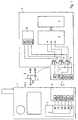
- FIG. 1shows a mobile terminal 1 for a wireless telecommunication system, as e.g. the GSM or the UMTS system.
- the mobile terminal 1comprises all necessary elements for the operation in a wireless telecommunication system, such as input keys, display, loudspeaker, microphone, antenna, and the like. For the sake of clarity, only the elements important and necessary for the present invention are shown.
- the mobile terminal 1comprises a terminal control means 2 for controlling the functions of the mobile terminal 1.
- the terminal control means 2may e.g. be a microcontroller, a microchip, or the like.
- the terminal control means 2is adapted to control the information exchange with a removable memory module 5 as shown in a first embodiment in figure 1 or a removable memory module 12 as shown in a second embodiment in figure 2. It is to be understood, that the removable memory modules 5 and 12 shown in figure 1 and 2, respectively, are only shown schematically and that their real sizes are considerably smaller as compared to the size of the mobile terminal 1 according to the present invention.
- the terminal control means 2 of the mobile terminal 1comprises a group 3 of input/output connections or input/output pins respectively being connected to a corresponding connection or terminal of an interface 4.
- the removable memory module 5 or 12is adapted to be removably connected to the interface 4, e.g. by means of a snap-in connection or the like.
- the interface 4 of the mobile terminal 1comprises, as shown in figure 1, a bus state connection BS connected with a corresponding bus state pin of the terminal control means 2 for providing a bus state signal to a connected memory module 5 or 12. Further, the interface 4 comprises a data input/output connection connected to a corresponding data input/output pin IO of the terminal control means 2 for exchanging input/output data with a connected memory module 5 or 12. The interface 4 further comprises a clock signal connection SCLK connected to a corresponding clock pin CLK of the terminal control means 2 for providing a clock signal to a connected removable memory module 5 or 12.
- the interface 4comprises a control voltage terminal VCC connected to a corresponding control voltage pin VCC of the terminal control means 2 for providing a control voltage to a connected removable memory module 5 or 12.
- the interface 4further comprises a steady voltage connection VSS connected to a corresponding steady voltage pin VSS of the terminal control means 2 for providing a steady voltage to a connected removable memory module 5 or 12.
- the steady voltage terminal VSS of the terminal control means 2is connected to ground.
- the interface 4may further comprise a reserve connection RES connected to a corresponding output pin OUT of the terminal control means 2.
- the reserve connection RESis e.g. a connection reserved for further use designed to have space for future extensions of the functionality.
- the terminal control means 2supplies a control signal via the output pin OUT and the reserve connection RES of the interface 4 to the connected removable memory module 5 in order to control the switching of the switch means 9 as explained below in more detail.
- the reserve connection of the interface 4is not needed to control the removable memory module 12.
- the removable memory module 5 shown in figure 1comprises a number of electrical connections or terminals to be connected with the connections BS, DIO, SCLK, VCC, VSS and RES of the interface 4 of the mobile terminal 1.
- the removable memory module 5further comprises a memory control means 6 for controlling a memory means 7.
- the memory control means 6may e.g. be a microprocessor, a microcontroller or the like.
- the memory means 7 controlled by the memory control means 6is a storage unit to which data can be written and from which data can be read.
- the removable memory module 5comprises a subscriber identity means 8 for providing subscriber identity information.
- the subscriber identity means 8is either a connector means for connecting a removable subscriber identity module card or comprises a subscriber memory means for storing subscriber identity information. In the latter case, the subscriber identity means 8 may further comprise a subscriber identity controller means for controlling the reading and writing of subscriber data from and to the subscriber memory means.
- Respective switch means 9selectively connect some of the connections or terminals of the removable memory module 5 with corresponding connections or terminals of the subscriber identity means 8 and the memory control means 6 in order to control and provide a data exchange as necessary.
- a first switch means 9is connected between the bus state signal connection BS of the memory module 5 a reset signal connection RST of the subscriber identity means 8 and a bus state signal connection of the memory control means 6.
- a second switch means 9is connected between the data input/output connection DIO of the memory module 5, a subscriber data input/output connection SIO of the subscriber identity means 8 and a data input/output connection of the memory control means 6.
- a third switch means 9is connected between the clock signal connection SCLK of the memory module 5, a clock signal connection CLK of the subscriber identity means 8 and a clock signal connection of the memory control means 6.
- the first, second and third switch means 9are connected to the reserve connection RES of the memory module 5 to be selectively and simultaneously switched between the respective connections of the memory control means 6 and the subscriber identity means 8.
- the first, second and third switch means 9may e.g. be configured as shown enlarged in figure 1.
- the first, second and third switch means 9respectively comprise a first diode 10 and a second diode 11.
- a control signal CTL supplied via the reserve connection RESis supplied directly to the first diode 10 but supplied as an inverted signal to the second diode 11.
- an input signal INas e.g. a signal supplied from one of the connections BS, DIO or SCLK, is either supplied via the first diode 10 to the respective connection of the subscriber identity means 8 or via the second diode 11 to the memory control means 6.
- the control means CTLis supplied from the terminal control means 2 via the OUT pin depending on which of the functionalities of the memory module 5 is required.
- the connections BS, DIO and SCLK of the memory module 5are selectively used by the subscriber identity means 8 or the memory control means 6 depending on which of the functionalities is requested by the terminal control means 2.
- the bus state signal supplied from the terminal control means 2 via the respective bus state signal connections BSis used in the subscriber identity module 8 as a reset signal.
- one or more clock signals supplied from the terminal control means 2 via the respective clock signal connections SCLKis used as a clock signal in the subscriber identity means 8.
- Subscriber identity datacan be supplied to the subscriber identity means 8 via the respective data input/output terminals DIO or read from the subscriber identity means 8 to the terminal control means 2.
- control voltage connection VCC and the steady voltage connection VSSare also connected to the memory control means 6 and/or the subscriber identity means 8 as necessary. However, their function is not important for the understanding of the present invention and thus no connections are shown. Further, the interface 4 as well as the removably memory module 5 may further comprise additional and not shown connections or terminals necessary for further functions as required.
- subscriber identity means 8which may comprise more than the three connections shown in figure 1 or figure 2, such as an additional connection for supplying a variable supply voltage, as e.g. a programming voltage or the like.
- the subscriber identity means 8 and the memory control means 6do not necessarily need the same number and kind of clock signals, so that the terminal control means 2 may supply the respectively necessary clock signals via the clock signal connections SCLK depending on which of the two units is addressed.
- the sameis true for the bus state signal supplied from the terminal control means 2 via the bus state signal connections, which may be varied depending on how the setting of the switch means 9 is.
- the terminal control means 2directly controls and changes the settings of the first, second and third switch means 9 by a control signal supplied via the reserved connections RES.
- the setting of the first, second and third switch means 9as directly changed upon the reception of a control signal from the terminal control means 2.
- FIG. 2shows a schematic diagram of a removable memory module 12 according to the second embodiment of the present invention.
- the essential features and units of the removable memory module 12correspond to the ones shown for and explained in relation to the removable memory module 5 shown in figure 1.
- the main differenceis that the reserve connection RES of the interface 4 is not necessary to supply a control signal for changing the settings of the switch means 13 and 14 connecting respective connections of the interface 4, the subscriber identity means 8 and the memory control means 6.
- the clock signal connection SCLK of the memory module 12is directly and steadily connected to the clock signal connection CLK of the subscriber identity means 8 and the clock signal connection CLK of the memory control means 6.
- a first switch means 13is connected between the bus state signal connection BS of the memory module 12, the reset signal connection RST of the subscriber identity means 8 and the bus state signal connection of the memory control means 6.
- a second switch means 14is connected between the data input/output connection DIE of the memory module 12, the data input/output connection IO of the subscriber identity means 8 and the data input/output connection of the memory control means 6.
- the first switch means 13 and the second switch means 14are respectively connected to and controlled via a switch control signal connection SWCTL of the memory control means 6.
- the first switch means 13is a three-state output controlled switch means like the first, second and third switch means 9 of the memory module 5 shown in figure 1, whereas the second switch means 15 of the memory module 12 only is a two-state output controlled switch.
- the first switch means 13selectively switches the bus state signal connection BS between the respective connections or terminals of the subscriber identity means 8 and the memory control means 6.
- the data input/output connection DIO of the memory module 12is constantly and directly connected to the data input/output connection IO of the memory control means 6.
- the second switch means 15is selectively connecting the data input/output connection DIO of the memory module 12 and the data input/output connection IO of the memory control means 6 with the data input/output connection IO of the subscriber identity means 8.
- the terminal control means 2 of the mobile terminal 1When the terminal control means 2 of the mobile terminal 1 first addresses the removable memory module 12, it sends a first command to the memory control means 6, e.g. via the bus state signal connection BS.
- the first switch means 13is thus normally switched to the memory control means 6 and the second switch means 14 is open (disconnected).
- the terminal control means 2wants to address the memory control means 6 and the memory means 7, the setting of the first switch 13 and the second switch 14 remains unchanged.
- the memory control means 6After the reception of a respective command, outputs a control signal via its switch control connection SWCTL which simultaneously switches the first switch means 13 and the second switch means 14 so that the subscriber identity means 8 can be addressed.
- the memory control means 6While the terminal control means 2 accesses the subscriber identity means 8, the data exchange is monitored by the memory control means 6.
- the memory control means 6recognizes the end of the data transfer between the terminal control means 2 and the subscriber identity means 8, e.g. after detecting that a certain time period has passed without any data having been sent, the memory control means 6 automatically outputs another control signal via the switch control connection SWCTL which switches the first switch means 13 and the second switch means 14 back to their original position.
- the memory module 12 according to the second embodimenthas, compared to the memory module 5 according to the first embodiment, the advantage that one connection less is required for controlling the setting of the switches. On the other hand, the required processing is more complex.
- the second switch means 14may comprise a diode 15.
- a control signal CTL supplied from the switch control connection tap SWCTL of the memory control means 6is supplied as an inverted signal to the diode 15 in order to selectively connect or disconnect the data input/output connection tap IO of the subscriber identity means 8.
- the configuration of the first switch means 13 of the memory module 12can e.g. correspond to the configuration of the switch means 9 shown enlarged in figure 1.
- the other functionalities and configurations of the subscriber identity means 8, the memory control means 6, the memory means 7 and the several connection taps of the memory module 15correspond identically to the functionalities and configurations respectively explained in relation to the memory module 5 shown in figure 1.
Landscapes
- Engineering & Computer Science (AREA)
- Databases & Information Systems (AREA)
- Computer Networks & Wireless Communication (AREA)
- Signal Processing (AREA)
- Mobile Radio Communication Systems (AREA)
- Telephone Function (AREA)
Abstract
Description
Claims (8)
- Mobile terminal (1) for a wireless telecommunication system, withwhereby said memory module (5, 12) further comprises a subscriber identity means (8)for providing subscriber identity information to said terminal control module (2) via atleast one of said several connections of said interface (4).a terminal control means (2) for controlling the functions of the mobile terminal, anda removable memory module (5, 12) comprising a memory means (7) and a memorycontrol means (6) for controlling the memory means (7),said memory module (5, 12) being removably connected to the terminal control means(2) by an interface (4) having several connections for exchanging information betweensaid terminal control means (2) and said memory control means (6),
- Mobile terminal according to claim 1,
characterized in,that said subscriber identity means (8) comprises a connector means for connecting aremovable subscriber identity module card. - Mobile terminal according to claim 1,
characterized in,that said subscriber identity means (8) comprises a subscriber memory means forstoring subscriber identity information. - Mobile terminal according to claim 1, 2 or 3,
characterized in,that said subscriber identity means (8) is connected via respective switch means(9, 13, 14) to said at least one of said several connections of said interface (4). - Mobile terminal according to claim 4,
characterized in,that said respective switch means (9, 13, 14) selectively switch a respective connectionof said interface (4) between said memory control means (6) and said subscriber identitymeans (8). - Mobile terminal according to claim 4 or 5,
characterized in,
said at least one connection selectively connected to said subscriber identity means (8)and said memory control means (6) is a data in/out connection. - Mobile terminal according to claim 4, 5 or 6,
characterized in,that said respective switch means (5) is controlled by said terminal control means (2). - Mobile terminal according to claim 4, 5 or 6,
characterized in,that said respective switch means (13, 14) is controlled by said memory controlmeans (6).
Priority Applications (2)
| Application Number | Priority Date | Filing Date | Title |
|---|---|---|---|
| EP20000120475EP1189465B1 (en) | 2000-09-19 | 2000-09-19 | Mobile terminal with removable memory having SIM card function |
| DE2000626768DE60026768T2 (en) | 2000-09-19 | 2000-09-19 | Mobile terminal with removable memory and SIM card function |
Applications Claiming Priority (1)
| Application Number | Priority Date | Filing Date | Title |
|---|---|---|---|
| EP20000120475EP1189465B1 (en) | 2000-09-19 | 2000-09-19 | Mobile terminal with removable memory having SIM card function |
Publications (2)
| Publication Number | Publication Date |
|---|---|
| EP1189465A1true EP1189465A1 (en) | 2002-03-20 |
| EP1189465B1 EP1189465B1 (en) | 2006-03-22 |
Family
ID=8169877
Family Applications (1)
| Application Number | Title | Priority Date | Filing Date |
|---|---|---|---|
| EP20000120475Expired - LifetimeEP1189465B1 (en) | 2000-09-19 | 2000-09-19 | Mobile terminal with removable memory having SIM card function |
Country Status (2)
| Country | Link |
|---|---|
| EP (1) | EP1189465B1 (en) |
| DE (1) | DE60026768T2 (en) |
Cited By (16)
| Publication number | Priority date | Publication date | Assignee | Title |
|---|---|---|---|---|
| KR100486525B1 (en)* | 2002-07-05 | 2005-05-03 | 엘지전자 주식회사 | Transport protocol data unit transmission method for mobile communication device |
| WO2006052293A1 (en)* | 2004-11-08 | 2006-05-18 | Sony Ericsson Mobile Communications Ab | Combined mass data storage and subscriber identity module |
| US7051169B2 (en)* | 2002-02-26 | 2006-05-23 | Kyocera Wireless Corp. | Memory configuration for a wireless communications device |
| WO2006108184A1 (en)* | 2005-04-07 | 2006-10-12 | Tyfone, Inc. | Sleeve for electronic transaction card |
| WO2007107166A1 (en)* | 2006-03-21 | 2007-09-27 | Anwar Reda Sedra Henein | Back-up device for a mobile telephone |
| DE102007006570A1 (en)* | 2007-02-09 | 2008-08-14 | Giesecke & Devrient Gmbh | Method for backing up data of a mobile terminal |
| CN100446600C (en)* | 2005-09-22 | 2008-12-24 | 华为技术有限公司 | System and method for expanding storage space of mobile terminal |
| WO2009106204A1 (en)* | 2008-02-29 | 2009-09-03 | T-Mobile International Ag | Memory card with integrated sim |
| US7856249B2 (en) | 2004-11-08 | 2010-12-21 | Sony Ericsson Mobile Communications Ab | Combined mass storage and subscriber identity module providing information security and apparatus for use therewith |
| US7954715B2 (en) | 2005-02-22 | 2011-06-07 | Tyfone, Inc. | Mobile device with transaction card in add-on slot |
| US7961101B2 (en) | 2008-08-08 | 2011-06-14 | Tyfone, Inc. | Small RFID card with integrated inductive element |
| US7991158B2 (en) | 2006-12-13 | 2011-08-02 | Tyfone, Inc. | Secure messaging |
| US8231061B2 (en) | 2009-02-24 | 2012-07-31 | Tyfone, Inc | Contactless device with miniaturized antenna |
| US8451122B2 (en) | 2008-08-08 | 2013-05-28 | Tyfone, Inc. | Smartcard performance enhancement circuits and systems |
| US9741027B2 (en) | 2007-12-14 | 2017-08-22 | Tyfone, Inc. | Memory card based contactless devices |
| US12147863B2 (en) | 2008-08-08 | 2024-11-19 | Icashe, Inc. | Method and apparatus for transmitting data via NFC for mobile applications including mobile payments and ticketing |
Citations (2)
| Publication number | Priority date | Publication date | Assignee | Title |
|---|---|---|---|---|
| US5633484A (en)* | 1994-12-26 | 1997-05-27 | Motorola, Inc. | Method and apparatus for personal attribute selection and management using a preference memory |
| FR2748834A1 (en)* | 1996-05-17 | 1997-11-21 | Gemplus Card Int | COMMUNICATION SYSTEM ALLOWING SECURE AND INDEPENDENT MANAGEMENT OF A PLURALITY OF APPLICATIONS BY EACH USER CARD, USER CARD AND CORRESPONDING MANAGEMENT METHOD |
- 2000
- 2000-09-19EPEP20000120475patent/EP1189465B1/ennot_activeExpired - Lifetime
- 2000-09-19DEDE2000626768patent/DE60026768T2/ennot_activeExpired - Lifetime
Patent Citations (2)
| Publication number | Priority date | Publication date | Assignee | Title |
|---|---|---|---|---|
| US5633484A (en)* | 1994-12-26 | 1997-05-27 | Motorola, Inc. | Method and apparatus for personal attribute selection and management using a preference memory |
| FR2748834A1 (en)* | 1996-05-17 | 1997-11-21 | Gemplus Card Int | COMMUNICATION SYSTEM ALLOWING SECURE AND INDEPENDENT MANAGEMENT OF A PLURALITY OF APPLICATIONS BY EACH USER CARD, USER CARD AND CORRESPONDING MANAGEMENT METHOD |
Cited By (52)
| Publication number | Priority date | Publication date | Assignee | Title |
|---|---|---|---|---|
| US7051169B2 (en)* | 2002-02-26 | 2006-05-23 | Kyocera Wireless Corp. | Memory configuration for a wireless communications device |
| KR100486525B1 (en)* | 2002-07-05 | 2005-05-03 | 엘지전자 주식회사 | Transport protocol data unit transmission method for mobile communication device |
| US7856249B2 (en) | 2004-11-08 | 2010-12-21 | Sony Ericsson Mobile Communications Ab | Combined mass storage and subscriber identity module providing information security and apparatus for use therewith |
| WO2006052293A1 (en)* | 2004-11-08 | 2006-05-18 | Sony Ericsson Mobile Communications Ab | Combined mass data storage and subscriber identity module |
| US8091786B2 (en) | 2005-02-22 | 2012-01-10 | Tyfone, Inc. | Add-on card with smartcard circuitry powered by a mobile device |
| US8083145B2 (en) | 2005-02-22 | 2011-12-27 | Tyfone, Inc. | Provisioning an add-on apparatus with smartcard circuity for enabling transactions |
| US9208423B1 (en) | 2005-02-22 | 2015-12-08 | Tyfone, Inc. | Mobile device with time-varying magnetic field and single transaction account numbers |
| US9202156B2 (en) | 2005-02-22 | 2015-12-01 | Tyfone, Inc. | Mobile device with time-varying magnetic field |
| US9626611B2 (en) | 2005-02-22 | 2017-04-18 | Tyfone, Inc. | Provisioning mobile device with time-varying magnetic field |
| US7954715B2 (en) | 2005-02-22 | 2011-06-07 | Tyfone, Inc. | Mobile device with transaction card in add-on slot |
| US7954717B2 (en) | 2005-02-22 | 2011-06-07 | Tyfone, Inc. | Provisioning electronic transaction card in mobile device |
| US7954716B2 (en) | 2005-02-22 | 2011-06-07 | Tyfone, Inc. | Electronic transaction card powered by mobile device |
| US9715649B2 (en) | 2005-02-22 | 2017-07-25 | Tyfone, Inc. | Device with current carrying conductor to produce time-varying magnetic field |
| US9092708B1 (en) | 2005-02-22 | 2015-07-28 | Tyfone, Inc. | Wearable device with time-varying magnetic field |
| US12223378B2 (en) | 2005-02-22 | 2025-02-11 | Icashe, Inc. | Electronic transaction mechanism |
| US9004361B2 (en) | 2005-02-22 | 2015-04-14 | Tyfone, Inc. | Wearable device transaction system |
| US9251453B1 (en) | 2005-02-22 | 2016-02-02 | Tyfone, Inc. | Wearable device with time-varying magnetic field and single transaction account numbers |
| US8136732B2 (en) | 2005-02-22 | 2012-03-20 | Tyfone, Inc. | Electronic transaction card with contactless interface |
| US11720777B2 (en) | 2005-02-22 | 2023-08-08 | Icashe, Inc. | Mobile phone with magnetic card emulation |
| US8408463B2 (en) | 2005-02-22 | 2013-04-02 | Tyfone, Inc. | Mobile device add-on apparatus for financial transactions |
| US11436461B2 (en) | 2005-02-22 | 2022-09-06 | Kepler Computing Inc. | Mobile phone with magnetic card emulation |
| US11270174B2 (en) | 2005-02-22 | 2022-03-08 | Icashe, Inc. | Mobile phone with magnetic card emulation |
| US8474718B2 (en) | 2005-02-22 | 2013-07-02 | Tyfone, Inc. | Method for provisioning an apparatus connected contactless to a mobile device |
| US8573494B2 (en) | 2005-02-22 | 2013-11-05 | Tyfone, Inc. | Apparatus for secure financial transactions |
| US10803370B2 (en) | 2005-02-22 | 2020-10-13 | Tyfone, Inc. | Provisioning wearable device with current carrying conductor to produce time-varying magnetic field |
| US10185909B2 (en) | 2005-02-22 | 2019-01-22 | Tyfone, Inc. | Wearable device with current carrying conductor to produce time-varying magnetic field |
| WO2006108184A1 (en)* | 2005-04-07 | 2006-10-12 | Tyfone, Inc. | Sleeve for electronic transaction card |
| CN100446600C (en)* | 2005-09-22 | 2008-12-24 | 华为技术有限公司 | System and method for expanding storage space of mobile terminal |
| WO2007107166A1 (en)* | 2006-03-21 | 2007-09-27 | Anwar Reda Sedra Henein | Back-up device for a mobile telephone |
| US7991158B2 (en) | 2006-12-13 | 2011-08-02 | Tyfone, Inc. | Secure messaging |
| DE102007006570A1 (en)* | 2007-02-09 | 2008-08-14 | Giesecke & Devrient Gmbh | Method for backing up data of a mobile terminal |
| US9741027B2 (en) | 2007-12-14 | 2017-08-22 | Tyfone, Inc. | Memory card based contactless devices |
| WO2009106204A1 (en)* | 2008-02-29 | 2009-09-03 | T-Mobile International Ag | Memory card with integrated sim |
| US7961101B2 (en) | 2008-08-08 | 2011-06-14 | Tyfone, Inc. | Small RFID card with integrated inductive element |
| US10318855B2 (en) | 2008-08-08 | 2019-06-11 | Tyfone, Inc. | Computing device with NFC and active load modulation for mass transit ticketing |
| US9483722B2 (en) | 2008-08-08 | 2016-11-01 | Tyfone, Inc. | Amplifier and transmission solution for 13.56MHz radio coupled to smartcard controller |
| US9489608B2 (en) | 2008-08-08 | 2016-11-08 | Tyfone, Inc. | Amplifier and transmission solution for 13.56MHz radio coupled to smartmx smartcard controller |
| US9122965B2 (en) | 2008-08-08 | 2015-09-01 | Tyfone, Inc. | 13.56 MHz enhancement circuit for smartcard controller |
| US9117152B2 (en) | 2008-08-08 | 2015-08-25 | Tyfone, Inc. | 13.56 MHz enhancement circuit for smartmx smartcard controller |
| US8937549B2 (en) | 2008-08-08 | 2015-01-20 | Tyfone, Inc. | Enhanced integrated circuit with smartcard controller |
| US9904887B2 (en) | 2008-08-08 | 2018-02-27 | Tyfone, Inc. | Computing device with NFC and active load modulation |
| US8866614B2 (en) | 2008-08-08 | 2014-10-21 | Tyfone, Inc. | Active circuit for RFID |
| US9390359B2 (en) | 2008-08-08 | 2016-07-12 | Tyfone, Inc. | Mobile device with a contactless smartcard device and active load modulation |
| US10607129B2 (en) | 2008-08-08 | 2020-03-31 | Tyfone, Inc. | Sideband generating NFC apparatus to mimic load modulation |
| US8814053B2 (en) | 2008-08-08 | 2014-08-26 | Tyfone, Inc. | Mobile payment device with small inductive device powered by a host device |
| US10949726B2 (en) | 2008-08-08 | 2021-03-16 | Icashe, Inc. | Mobile phone with NFC apparatus that does not rely on power derived from an interrogating RF field |
| US8451122B2 (en) | 2008-08-08 | 2013-05-28 | Tyfone, Inc. | Smartcard performance enhancement circuits and systems |
| US8410936B2 (en) | 2008-08-08 | 2013-04-02 | Tyfone, Inc. | Contactless card that receives power from host device |
| US11694053B2 (en) | 2008-08-08 | 2023-07-04 | Icashe, Inc. | Method and apparatus for transmitting data via NFC for mobile applications including mobile payments and ticketing |
| US8072331B2 (en) | 2008-08-08 | 2011-12-06 | Tyfone, Inc. | Mobile payment device |
| US12147863B2 (en) | 2008-08-08 | 2024-11-19 | Icashe, Inc. | Method and apparatus for transmitting data via NFC for mobile applications including mobile payments and ticketing |
| US8231061B2 (en) | 2009-02-24 | 2012-07-31 | Tyfone, Inc | Contactless device with miniaturized antenna |
Also Published As
| Publication number | Publication date |
|---|---|
| DE60026768D1 (en) | 2006-05-11 |
| EP1189465B1 (en) | 2006-03-22 |
| DE60026768T2 (en) | 2006-11-09 |
Similar Documents
| Publication | Publication Date | Title |
|---|---|---|
| EP1189465B1 (en) | Mobile terminal with removable memory having SIM card function | |
| US8433840B2 (en) | Storage card having selectable contact elements and method of its operation | |
| EP2075744B1 (en) | A dual mode smart card controller for a smart card reader | |
| US8544752B2 (en) | Nonvolatile memory card adaptable to plural specifications | |
| EP1597696B1 (en) | Multi-protocol memory card | |
| CN100469079C (en) | Dual-mode dual-standby mobile phone with dual card slots and its implementation method | |
| JP2006217586A (en) | Dual universal integrated circuit card (uicc) system for portable device | |
| US7219846B2 (en) | Circuit module and memory card kit compliant with various access protocols | |
| KR100556853B1 (en) | SIM card access device of mobile terminal | |
| WO2005086583A2 (en) | System, apparatus and method for sharing media | |
| CN101025782A (en) | Method and apparatus for contactless interface on ICC supporting high speed interface | |
| US8560007B2 (en) | Apparatus and method for supporting different types of universal integrated circuit cards | |
| CN102549605B (en) | For the electronic circuit of the intelligent card chip that interconnects | |
| CN111598206A (en) | Multifunctional SIM card and terminal equipment | |
| EP2304729B1 (en) | Memory card adapter | |
| EP0564105A2 (en) | Memory module adapter | |
| CN101883176A (en) | Expansion card processing method, device and mobile terminal | |
| KR200438503Y1 (en) | Smart Card Adapter for Mobile Devices | |
| EP3697172B1 (en) | Memory card and mobile terminal | |
| KR100455990B1 (en) | Mobile wireless device with user identify card sharing memory card | |
| EP3737128B1 (en) | Common data and clock signal lines | |
| KR100855262B1 (en) | Nonvolatile Memory Card Adapts to Multiple Specifications | |
| KR200341165Y1 (en) | USB connection device by using data port of portable phone | |
| KR200339123Y1 (en) | Structure for Installing Card in Mobile Telecommunication Terminal | |
| CN102254198A (en) | Data transmitting method for expansion microSD card and user identification module |
Legal Events
| Date | Code | Title | Description |
|---|---|---|---|
| PUAI | Public reference made under article 153(3) epc to a published international application that has entered the european phase | Free format text:ORIGINAL CODE: 0009012 | |
| AK | Designated contracting states | Kind code of ref document:A1 Designated state(s):AT BE CH CY DE DK ES FI FR GB GR IE IT LI LU MC NL PT SE Kind code of ref document:A1 Designated state(s):DE FR GB | |
| AX | Request for extension of the european patent | Free format text:AL;LT;LV;MK;RO;SI | |
| 17P | Request for examination filed | Effective date:20020522 | |
| AKX | Designation fees paid | Free format text:DE FR GB | |
| 17Q | First examination report despatched | Effective date:20041007 | |
| GRAP | Despatch of communication of intention to grant a patent | Free format text:ORIGINAL CODE: EPIDOSNIGR1 | |
| GRAS | Grant fee paid | Free format text:ORIGINAL CODE: EPIDOSNIGR3 | |
| RAP1 | Party data changed (applicant data changed or rights of an application transferred) | Owner name:SONY DEUTSCHLAND GMBH | |
| RAP1 | Party data changed (applicant data changed or rights of an application transferred) | Owner name:SONY DEUTSCHLAND GMBH | |
| RAP1 | Party data changed (applicant data changed or rights of an application transferred) | Owner name:SONY DEUTSCHLAND GMBH | |
| GRAA | (expected) grant | Free format text:ORIGINAL CODE: 0009210 | |
| AK | Designated contracting states | Kind code of ref document:B1 Designated state(s):DE FR GB | |
| REG | Reference to a national code | Ref country code:GB Ref legal event code:FG4D | |
| RIN1 | Information on inventor provided before grant (corrected) | Inventor name:YAMAGISHI, YUTAKA,DIGITAL TELECOMM. EUROPE Inventor name:CHRISTENSEN, PER HARTMANN Inventor name:USHINO, TATSUJI,DIGITAL TELECOMMUNICATIONS EUROPE | |
| REF | Corresponds to: | Ref document number:60026768 Country of ref document:DE Date of ref document:20060511 Kind code of ref document:P | |
| ET | Fr: translation filed | ||
| PLBE | No opposition filed within time limit | Free format text:ORIGINAL CODE: 0009261 | |
| STAA | Information on the status of an ep patent application or granted ep patent | Free format text:STATUS: NO OPPOSITION FILED WITHIN TIME LIMIT | |
| 26N | No opposition filed | Effective date:20061227 | |
| PGFP | Annual fee paid to national office [announced via postgrant information from national office to epo] | Ref country code:FR Payment date:20110928 Year of fee payment:12 | |
| REG | Reference to a national code | Ref country code:FR Ref legal event code:ST Effective date:20130531 | |
| PG25 | Lapsed in a contracting state [announced via postgrant information from national office to epo] | Ref country code:FR Free format text:LAPSE BECAUSE OF NON-PAYMENT OF DUE FEES Effective date:20121001 | |
| PGFP | Annual fee paid to national office [announced via postgrant information from national office to epo] | Ref country code:DE Payment date:20140922 Year of fee payment:15 | |
| PGFP | Annual fee paid to national office [announced via postgrant information from national office to epo] | Ref country code:GB Payment date:20140919 Year of fee payment:15 | |
| REG | Reference to a national code | Ref country code:DE Ref legal event code:R119 Ref document number:60026768 Country of ref document:DE | |
| GBPC | Gb: european patent ceased through non-payment of renewal fee | Effective date:20150919 | |
| PG25 | Lapsed in a contracting state [announced via postgrant information from national office to epo] | Ref country code:DE Free format text:LAPSE BECAUSE OF NON-PAYMENT OF DUE FEES Effective date:20160401 Ref country code:GB Free format text:LAPSE BECAUSE OF NON-PAYMENT OF DUE FEES Effective date:20150919 |