EP1181768B1 - Linearisation and modulation device - Google Patents
Linearisation and modulation deviceDownload PDFInfo
- Publication number
- EP1181768B1 EP1181768B1EP99925037AEP99925037AEP1181768B1EP 1181768 B1EP1181768 B1EP 1181768B1EP 99925037 AEP99925037 AEP 99925037AEP 99925037 AEP99925037 AEP 99925037AEP 1181768 B1EP1181768 B1EP 1181768B1
- Authority
- EP
- European Patent Office
- Prior art keywords
- signal
- digital
- linearisation
- correction value
- modulation device
- Prior art date
- Legal status (The legal status is an assumption and is not a legal conclusion. Google has not performed a legal analysis and makes no representation as to the accuracy of the status listed.)
- Expired - Lifetime
Links
- 238000012937correctionMethods0.000claimsdescription71
- 239000013598vectorSubstances0.000claimsdescription25
- 230000006978adaptationEffects0.000claimsdescription15
- 230000007274generation of a signal involved in cell-cell signalingEffects0.000claimsdescription4
- 238000000034methodMethods0.000description4
- 238000001228spectrumMethods0.000description4
- 208000024269Mucopolysaccharidosis-like syndrome with congenital heart defects and hematopoietic diseaseDiseases0.000description3
- 238000012545processingMethods0.000description3
- 230000015556catabolic processEffects0.000description2
- 238000006243chemical reactionMethods0.000description2
- 238000004891communicationMethods0.000description2
- 238000006731degradation reactionMethods0.000description2
- 238000010295mobile communicationMethods0.000description2
- QTYLEXQVLJYJHT-UHFFFAOYSA-N2-(2-fluorophenyl)-3-methylmorpholineChemical compoundCC1NCCOC1C1=CC=CC=C1FQTYLEXQVLJYJHT-UHFFFAOYSA-N0.000description1
- 230000003044adaptive effectEffects0.000description1
- 230000005540biological transmissionEffects0.000description1
- 230000015572biosynthetic processEffects0.000description1
- 239000000969carrierSubstances0.000description1
- 238000010276constructionMethods0.000description1
- 230000001419dependent effectEffects0.000description1
- 238000011161developmentMethods0.000description1
- 230000018109developmental processEffects0.000description1
- 230000000694effectsEffects0.000description1
- 238000001914filtrationMethods0.000description1
- 238000005259measurementMethods0.000description1
- 238000003786synthesis reactionMethods0.000description1
Images


Classifications
- H—ELECTRICITY
- H03—ELECTRONIC CIRCUITRY
- H03C—MODULATION
- H03C3/00—Angle modulation
- H03C3/38—Angle modulation by converting amplitude modulation to angle modulation
- H03C3/40—Angle modulation by converting amplitude modulation to angle modulation using two signal paths the outputs of which have a predetermined phase difference and at least one output being amplitude-modulated
- H—ELECTRICITY
- H03—ELECTRONIC CIRCUITRY
- H03F—AMPLIFIERS
- H03F1/00—Details of amplifiers with only discharge tubes, only semiconductor devices or only unspecified devices as amplifying elements
- H03F1/32—Modifications of amplifiers to reduce non-linear distortion
- H03F1/3241—Modifications of amplifiers to reduce non-linear distortion using predistortion circuits
- H03F1/3247—Modifications of amplifiers to reduce non-linear distortion using predistortion circuits using feedback acting on predistortion circuits
- H—ELECTRICITY
- H03—ELECTRONIC CIRCUITRY
- H03F—AMPLIFIERS
- H03F1/00—Details of amplifiers with only discharge tubes, only semiconductor devices or only unspecified devices as amplifying elements
- H03F1/32—Modifications of amplifiers to reduce non-linear distortion
- H03F1/3241—Modifications of amplifiers to reduce non-linear distortion using predistortion circuits
- H03F1/3282—Acting on the phase and the amplitude of the input signal
- H03F1/3288—Acting on the phase and the amplitude of the input signal to compensate phase shift as a function of the amplitude
- H—ELECTRICITY
- H04—ELECTRIC COMMUNICATION TECHNIQUE
- H04L—TRANSMISSION OF DIGITAL INFORMATION, e.g. TELEGRAPHIC COMMUNICATION
- H04L27/00—Modulated-carrier systems
- H04L27/32—Carrier systems characterised by combinations of two or more of the types covered by groups H04L27/02, H04L27/10, H04L27/18 or H04L27/26
- H04L27/34—Amplitude- and phase-modulated carrier systems, e.g. quadrature-amplitude modulated carrier systems
- H04L27/36—Modulator circuits; Transmitter circuits
- H04L27/366—Arrangements for compensating undesirable properties of the transmission path between the modulator and the demodulator
- H04L27/367—Arrangements for compensating undesirable properties of the transmission path between the modulator and the demodulator using predistortion
- H04L27/368—Arrangements for compensating undesirable properties of the transmission path between the modulator and the demodulator using predistortion adaptive predistortion
- H—ELECTRICITY
- H03—ELECTRONIC CIRCUITRY
- H03F—AMPLIFIERS
- H03F2201/00—Indexing scheme relating to details of amplifiers with only discharge tubes, only semiconductor devices or only unspecified devices as amplifying elements covered by H03F1/00
- H03F2201/32—Indexing scheme relating to modifications of amplifiers to reduce non-linear distortion
- H03F2201/3233—Adaptive predistortion using lookup table, e.g. memory, RAM, ROM, LUT, to generate the predistortion
Definitions
- the present inventionrelates to a linearisation and modulation device, and especially to a combined digital predistortion and DDS vector modulator linearisation device for a power amplifier.
- an RF signal to be transmitted via an antennais usually modulated from two baseband signals which are orthogonal to each other.
- One signalis an in-phase signal (I signal)
- the other signalis a quadrature-phase signal (Q signal).
- I and Qbaseband signals
- I and Qare converted to a bandpass signal by an IQ mixer.
- the principle of such an IQ-mixeris described with reference to Fig. 6. Inside the IQ mixer the I signal is modulated with an in-phase carrier and the Q signal is modulated with a quadrature-phase carrier. The modulated signals are summed together to form a bandpass signal.
- the conversion from the baseband signals to the bandpass signalcan be effected directly to a radio frequency (RF) signal or first to an intermediate frequency (IF) signal and then to an RF signal.
- RFradio frequency
- IFintermediate frequency
- a digital IQ mixerthe signal is first converted to a digital IF signal, which is then converted to analogue form by means of a digital-analogue (D/A) converter.
- D/Adigital-analogue
- This analogue signalis then upconverted to an RF signal, or even firstly to a second IF signal and then to the RF signal.
- the RF signalBefore the RF signal is supplied to the antenna, it has to be amplified by a power amplifier PA.
- the power amplifieris power-efficient and at the same time shows a very low non-linear distortion in order to prevent a degradation of the RF signal to be transmitted.
- available power amplifierssuffer from non-linear characteristics. In the frequency domain, the effect of such a non-linear power amplifier occurs as a widening of the original spectrum.
- a predistortion methodAccording to this method, a predistortion signal is added to the input signal of a power amplifier. The predistortion signal is chosen such that the distortion generated in the power amplifier is cancelled.
- the basic structure according to this solutionis shown in Fig. 8, according to which a predistorter 61 adds a predistortion signal to a use signal x(t) which is to be amplified by a power amplifier 62.
- the non-linear distortion generated in the power amplifier 62is eliminated as described in the following.
- the predistortioncan be implemented in analogue form or can be effected by digital signal processing. In the latter case, a digital-analogue converter and a band-pass filter have to be provided between the predistorter 61 and the power amplifier 62.
- Upsampling meansinclude a sample rate expander and a low pass filter. For example, samples are read into the upsampling means by 4 MSPS (million samples per second) and samples are output by 16 MPSPS. This is done by first adding three zeros between the 4 MPSPS samples, so that the rate is changed to 16 MPSPS. This new sequence is then low-pass filtered in order to eliminate the image caused by the original rate.
- a sample-rate expansioncould also be effected by repeating the original sample, but this adds a sinc-response (in the frequency domain) to the signal and in this case it must be compensated for in the following filter.
- the digital baseband signals IIN and QIN output from the upsampling means 71 and 72are multiplied by multipliers 73 and 74 by an in-phase signal (cosine signal) and a quadrature-phase signal (sine signal), respectively, which are supplied for a DDS carrier generator 76.
- the output signals of the multipliers 73 and 74are added by an adder 75, and a resultant IF signal IF_OUT is output.
- this output signal IF_OUTis converted to an RF signal and then supplied to an RF power amplifier in order to supply it to an antenna.
- a complicated structureis required wherein first the modulation and then a linearisation of the power amplifier have to performed, which can be effected by the predistortion as described above, for example.
- a large spaceis required for the whole circuit.
- the signalsare affected by noises, especially when the above mentioned linearisation using the predistortion method is performed in an analogue form.
- the document EP-A-0 658 975discloses a baseband predistortion scheme for adaptive linearisation of power amplifiers. As shown in fig. 2, it teaches the use of correction value means generating amplitude (err- ⁇ ) and phase correction values (err- ⁇ ), amplitude and phase correction means (pre-distortion) and carrier signal generation means (fig. 1, DEM). However, both the amplitude and the phase information are passed back to determine the correction values.
- the document US-A-5 448 203teaches a scheme (see fig. 1) in which phase correction of the carrier generator (6) is performed, however, only on the basis of an abstract correction indication circuit (1) not necessarily using the digital baseband signals. In the document EP-A-0 823 805 the modulation (65, OL) is performed independent of the predistortion.
- the object underlying the present inventionresides in providing a device by which the above described drawbacks are removed.
- the linearisation and modulation devicecomprises a digital vector modulator for generating a modulated digital signal on the basis of digital baseband signals and digital carrier signals; a correction value generating means for generating an amplitude correction value and a phase correction value on the basis of said digital baseband signals and on the basis of a non-linearity distortion generated in said power amplifier arranged in a subsequent stage; an amplitude correction means for generating a corrected digital signal on the basis of said modulated digital signal and said amplitude correction value; a phase correction means for generating a corrected phase control signal on the basis of said phase correction value and an output signal of a phase control signal generation means; and a carrier signal generating means for generating said carrier signals on the basis of an output of said phase correction means.
- a compact devicecan be constructed in which the modulation and the linearisation are performed simultaneously.
- the systemis less affected by disturbances.
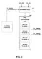
- Reference numeral 101denotes an upsampling means receiving a digital in-phase (I) signal IIN_BB for upsampling I signal IIN_BB. This is effected as mentioned above, that is, by increasing the sample rate (adding zero values between the original sample values) and by low pass filtering the expanded signal.
- the upsampling means 101outputs a digital I signal IIN which is supplied to a first multiplier 103.
- Reference numeral 102denotes an upsampling means receiving a digital quadrature-phase (Q) signal QIN_BB similar to the upsampling means 101.
- the upsampling means 102outputs a digital quadrature-phase signal QIN which is supplied to a second multiplier 104.
- the multipliers 103 and 104receive a sine signal (quadrature-phase signal) PH_S and a cosine signal (in-phase signal) PH_C, respectively, supplied from a DDS carrier generation means 112 which will be described later.
- the outputs of the multipliers 103 and 104are supplied to an adder 105.
- the output signal of the adder 105represents a modulated IF (intermediate frequency) signal IF_MOD.
- Fig. 2the address calculation means 114 and the predistortion LUT 108 are shown in more detail.
- the signal TX_FREQ indicating the transmitting frequencyis provided by a system controller.
- the predistortion LUT 108a plurality of sections PD-LUT TX BAND 1 to 4 are provided, each section comprising correction value for a specific frequency. Thus, a coarse frequency dependence of the predistortion can be provided.
- the phase correction value CV_AMPM read out of the predistortion LUT 108is supplied to an adder 111.
- the adder 111further receives a phase control signal from a phase accumulator (phase control signal generating means) 110.
- the adderoutputs a corrected phase control signal in which the phase is shifted relative to the input phase control signal according to the phase correction value CV_AMPM.
- the adder 11represents a phase correction means.
- the corrected phase control signal of the adder 111is supplied to the above mentioned DDS carrier signal generating means 112 which outputs a digital sine phase signal PH_S and a digital cosine phase signal PH_C which are supplied to the multipliers 103 and 104, respectively.
- the amplitude correction signal CV_AMAMis supplied to a shift register 113 serving to match a signal delay caused by the multipliers 103 and 104 and the adder 105.
- the output of the shift register 113is supplied to a further multiplier 106.
- the multiplier 106receives the modulated IF signal IF_MOD of the adder 105.
- the multiplier 106multiplies the modulated IF signal IF_MOD by the amplitude correction value CV_AMAM.
- the multiplier 106represents an amplitude correction means.
- the output of the multiplier 106is supplied to a rounding means 107 for rounding the resultant signal on an appropriate bit number, for example, 12 bits, as required for a subsequent stage to which the output signal IF_OUT is supplied.
- a sinc correction means 115is provided which compensates the output signal IF_OUT for the sinc response caused by a D/A converter in a following stage.
- the linearisation of a power amplifier in a subsequent stagei.e., the predistortion of the intermediate frequency signal is effected in the modulator. That is, the phase is corrected in the adder 111, i.e., the phase correction means, and the amplitude is corrected in the multiplier 106, i.e., the amplitude correction means.
- the adder 111i.e., the phase correction means
- the amplitudeis corrected in the multiplier 106, i.e., the amplitude correction means.
- the linearisationis performed by adding predetermined predistortion correction values which are selected only in dependence on the input baseband signals IIN_BB and QIN_BB.
- predetermined predistortion correction valueswhich are selected only in dependence on the input baseband signals IIN_BB and QIN_BB.
- the use of fixed predetermined valuesis sufficient in case the characteristic of the power amplifier does not change during operation. That is, the amplifier parameters may not deviate from preset values or only deviate to a relative small amount.
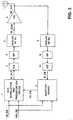
- Fig. 3shows a linearisation system including such an adaptation.
- Reference numeral 1denotes a linearisation and modulation device according to the second embodiment.
- the linearisation and modulation device 1supplies an output signal IF_OUT to a digital-analogue converter 3 which supplies an output signal to a band-pass filter 4.
- the analogue output signal of the band-pass filter 4is supplied to an analogue high frequency transmission circuit (analogue RF TX) 5 in which the analogue IF signal is upconverted to a desired TX frequency.
- the digital-analogue converter 3, the band-pass filter 4 and the analogue RF TX 5serve as a signal converting means for converting the digital intermediate frequency signal IF_OUT to an analogue RF signal RF_CON.
- the analogue RF signal RF_CONis supplied to a power amplifier 6 which amplifies the analogue RF signal and supplies the resultant RF signal RF_OUT to an antenna 7.
- correction valuesare obtained from the RF signal RF_OUT.
- a receiver structureis included in the feedback path.
- the RF signal RF_OUTis supplied to an analogue RF receiver circuit (analogue RF RX) 8 which downconverts the RF signal.
- the output signal of the analogue RF RX 8is supplied to a band-pass filter 9 which supplies its output signal to an analogue-digital converter 10.
- the analogue-digital converter 10outputs a digital feedback signal IF_FB.
- the analogue RF RX 8, the band-pass filter 9 and the analogue-digital converter 10serve as a signal de-converting means for converting the analogue RF signal RF to the digital feedback signal IF_FB.
- the digital feedback signal IF_FBis supplied to the adaptation device 2.
- the adaptation device 2also receives the baseband signals IIN_BB and QIN_BB. Based on the feedback signal IF_FB and the baseband signals IIN_BB and QIN_BB, the adaptation device 2 generates a feedback correction value CV_FB.
- the feedback correction value CV_FBis supplied to the linearisation and modulation device 1.
- the linearisation and modulation device 1is described in more detail with respect to Fig. 4.
- the linearisation and modulation device 1 according to the second embodimentis basically the same as that according to the first embodiment described with reference to Fig. 1, with the exception that the predistortion LUT is modified.
- the modified predistortion LUT 108ais a dual-port RAM. That is, new amplitude and phase correction values FAM and FPM can be written into the predistortion LUT 108a while the predistortion values CV_AMAM and CV_AMPM are read out via the first port.
- the new correction values FAM and FPMare generated from the feedback correction value CV_FB by means of a demultiplexer 109.
- the new correction valuesare written into the predistortion LUT 108a at an address which is determined in the same way as during reading out the predistortion values CV_AMAM and CV_AMPM, i.e. by using the baseband signals QIN_BB and IIN_BB and also the frequency TX_FREQ, if desired. This is effected by an accordingly adapted address calculation means 114a.
- the calculation of the feedback correction valuescan be based on 1) a comparison of input and feedback vectors, or 2) a measurement of adjacent channel power.
- the comparison between the input vector IN_BB consisting of the components IIN_BB and QIN_BB, and the feedback vector IF_FBis described in more detail with reference to Fig. 5.
- the input vector IN_BBis already decomposed in its components IIN_BB and QIN_BB.
- the multipliersalso receive a sine signal PH_S and a cosine signal PH_C, respectively, which are supplied from a DDS carrier generating means 206.
- the DDS carrier generating means 206generates the sine and cosine signals on the basis of a phase control signal received from a phase accumulator 205.
- the multipliersgenerate an in-phase signal and a quadrature-phase signal which are supplied to digital low-pass filters 203 and 204, respectively.
- the outputs I_FB and Q_FB of the digital low-pass filters 203 and 204are supplied to comparators 207 and 208, respectively.
- the outputs of the comparators 207 and 208represent the differences between the components of the input vector IN_BB and the feedback vector IF_FB and are supplied to a correction value calculator 209.
- the correction value calculator 209calculates a new correction value CV_FB. It is to be noted that CV_FB is a vector.
- the correction valuesare calculated after adjusting the time delay between the input vector IN_BB and the feedback vector IF_FB.
- vectors IN_BB (n) and IF_FB(n)are complex numbers. It is noted that the correction values are presented in polar coordinates.
- FPMFq Fi
Landscapes
- Engineering & Computer Science (AREA)
- Physics & Mathematics (AREA)
- Nonlinear Science (AREA)
- Power Engineering (AREA)
- Computer Networks & Wireless Communication (AREA)
- Signal Processing (AREA)
- Amplifiers (AREA)
- Digital Transmission Methods That Use Modulated Carrier Waves (AREA)
Description
- The present invention relates to a linearisation andmodulation device, and especially to a combined digitalpredistortion and DDS vector modulator linearisationdevice for a power amplifier.
- In the field of radio communication, an RF signal to betransmitted via an antenna, for example, is usuallymodulated from two baseband signals which are orthogonalto each other. One signal is an in-phase signal (Isignal), and the other signal is a quadrature-phasesignal (Q signal). These baseband signals (I and Q) areconverted to a bandpass signal by an IQ mixer. Theprinciple of such an IQ-mixer is described with referenceto Fig. 6. Inside the IQ mixer the I signal is modulatedwith an in-phase carrier and the Q signal is modulatedwith a quadrature-phase carrier. The modulated signalsare summed together to form a bandpass signal.
- The conversion from the baseband signals to the bandpasssignal can be effected directly to a radio frequency (RF)signal or first to an intermediate frequency (IF) signaland then to an RF signal. In a digital IQ mixer thesignal is first converted to a digital IF signal, whichis then converted to analogue form by means of a digital-analogue(D/A) converter. This analogue signal is thenupconverted to an RF signal, or even firstly to a secondIF signal and then to the RF signal. This is because of the limitation of speed of digital devices and DAconverters. However, since the processing speed ofdigital devices is currently increasing, it might bepossible in the future to convert signals directly intoan RF signal also by means of a digital device.
- Before the RF signal is supplied to the antenna, it hasto be amplified by a power amplifier PA.
- In such an arrangement, it is essential that the poweramplifier is power-efficient and at the same time shows avery low non-linear distortion in order to prevent adegradation of the RF signal to be transmitted. However,available power amplifiers suffer from non-linearcharacteristics. In the frequency domain, the effect ofsuch a non-linear power amplifier occurs as a widening ofthe original spectrum.
- In Fig. 7, spectrums of four channels are shown, wherein
channel 3 exhibits the above-mentioned widening of thespectrum. Thus, an interference with theadjacentchannels - Several different solutions have been proposed to copewith this situation. One solution is the so-calledpredistortion method. According to this method, apredistortion signal is added to the input signal of apower amplifier. The predistortion signal is chosen suchthat the distortion generated in the power amplifier iscancelled. The basic structure according to this solutionis shown in Fig. 8, according to which a
predistorter 61adds a predistortion signal to a use signal x(t) which isto be amplified by apower amplifier 62. The non-linear distortion generated in thepower amplifier 62 iseliminated as described in the following. - The distortion caused by the power amplifier can beexpressed by
- The
predistorter 61 adds a predistortion to the signal:poweramplifier 62. - Thus, the output signal of the
power amplifier 62 is - If the function p is inverse to the function of g(p= g-1), the resultant output signal is:
- Hence, the distortion is cancelled.
- The predistortion can be implemented in analogue form orcan be effected by digital signal processing. In thelatter case, a digital-analogue converter and a band-passfilter have to be provided between the
predistorter 61and thepower amplifier 62. - On the other hand, as mentioned above, in a transmittingsystem a modulation has to be performed, in which anintermediate frequency signal (IF signal) is generatedfrom in-phase and quadrature-phase signals (I and Qsignals). For this purpose, the I signal and the Q signalare multiplied with a sine signal and a cosine signal,respectively. This modulation is usually performed inanalogue form, but recently also a digital processing ofthis modulation has been proposed. This is called a DDS(Direct Digital Synthesis) and vector modulation. Thebasic structure of the DDS and vector modulation is shownin Fig. 9. The input baseband signals IIN_BB and QIN_BBare supplied to upsampling means 71 and 72, respectively.
- Upsampling means (interpolation means) include a samplerate expander and a low pass filter. For example, samplesare read into the upsampling means by 4 MSPS (millionsamples per second) and samples are output by 16 MPSPS.This is done by first adding three zeros between the 4MPSPS samples, so that the rate is changed to 16 MPSPS.This new sequence is then low-pass filtered in order toeliminate the image caused by the original rate. Asample-rate expansion could also be effected by repeatingthe original sample, but this adds a sinc-response (inthe frequency domain) to the signal and in this case itmust be compensated for in the following filter.
- The digital baseband signals IIN and QIN output from theupsampling means 71 and 72 are multiplied by
multipliers multipliers adder 75, and a resultant IF signal IF_OUT is output. - Conventionally, this output signal IF_OUT is converted toan RF signal and then supplied to an RF power amplifierin order to supply it to an antenna. Hence, for a wholemodulation and amplifier system, a complicated structureis required wherein first the modulation and then alinearisation of the power amplifier have to performed,which can be effected by the predistortion as describedabove, for example. Thus, a large space is required forthe whole circuit.
- Moreover, due to the large number of separate units, thesignals are affected by noises, especially when the abovementioned linearisation using the predistortion method isperformed in an analogue form.
- On the other hand, if it is performed in digital form,digital-analogue and analogue-digital converters have tobe included which in addition can cause degradation ofthe signals.
- The document EP-A-0 658 975 discloses a baseband predistortion scheme for adaptivelinearisation of power amplifiers. As shown in fig. 2, it teaches the use of correctionvalue means generating amplitude (err-ρ) and phase correction values (err-),amplitude and phase correction means (pre-distortion) and carrier signal generationmeans (fig. 1, DEM). However, both the amplitude and the phase information arepassed back to determine the correction values. The document US-A-5 448 203teaches a scheme (see fig. 1) in which phase correction of the carrier generator (6) isperformed, however, only on the basis of an abstract correction indication circuit (1) notnecessarily using the digital baseband signals. In the document EP-A-0 823 805 themodulation (65, OL) is performed independent of the predistortion.
- Hence, the object underlying the present inventionresides in providing a device by which the abovedescribed drawbacks are removed.
- This object is achieved by a linearisation and modulationdevice according to the present invention for a poweramplifier. The linearisation and modulation deviceaccording to the invention comprises a digital vectormodulator for generating a modulated digital signal onthe basis of digital baseband signals and digital carriersignals; a correction value generating means forgenerating an amplitude correction value and a phase correction value on the basis of said digital basebandsignals and on the basis of a non-linearity distortiongenerated in said power amplifier arranged in asubsequent stage; an amplitude correction means forgenerating a corrected digital signal on the basis ofsaid modulated digital signal and said amplitudecorrection value; a phase correction means for generatinga corrected phase control signal on the basis of saidphase correction value and an output signal of a phasecontrol signal generation means; and a carrier signalgenerating means for generating said carrier signals onthe basis of an output of said phase correction means.
- With such a device, a compact device can be constructedin which the modulation and the linearisation areperformed simultaneously.
- Thus, in case the modulation and linearisation deviceaccording to the invention is applied in a transmittingsystem for mobile communication, for example, the systemcan be made very compact.
- Furthermore, since the digital predistortion and themodulation are performed together in one circuit, thesystem is less affected by disturbances.
- Further advantageous developments are defined in thedependent claims.
- The present invention will be more readily understoodwith reference to the accompanying drawings in which:
- Fig. 1 shows the structure of a combined digitalpredistortion and DDS vector modulator for an RF poweramplifier according to a first embodiment of theinvention,
- Fig. 2 shows a predistortion LUT of Fig. 1 in moredetail,
- Fig. 3 shows a combined digital predistortion and DDSvector modulator included in a feedback linearisationsystem according to a second embodiment,
- Fig. 4 shows the combined digital predistortion and DDSvector modulator of Fig. 3,
- Fig. 5 shows a DDS vector modulator used in an
adaptationdevice 2 shown in Fig. 3, - Fig. 6 shows a an IQ-mixer,
- Fig. 7 shows a spectrum widening caused by a non-linearamplifier,
- Fig. 8 shows a power amplifier with a predistorter, and
- Fig. 9 shows a vector modulator with DDS carriers.
- In the following, embodiments of the invention aredescribed in more detail with reference to theaccompanying drawings.
- Fig. 1 shows the general construction of a combineddigital predistortion and DDS vector modulationlinearisation device (in the following referred to as alinearisation and modulation device) according to theinvention.
Reference numeral 101 denotes an upsampling meansreceiving a digital in-phase (I) signal IIN_BB forupsampling I signal IIN_BB. This is effected as mentionedabove, that is, by increasing the sample rate (addingzero values between the original sample values) and bylow pass filtering the expanded signal. The upsamplingmeans 101 outputs a digital I signal IIN which issupplied to afirst multiplier 103.Reference numeral 102denotes an upsampling means receiving a digitalquadrature-phase (Q) signal QIN_BB similar to theupsampling means 101. The upsampling means 102 outputs adigital quadrature-phase signal QIN which is supplied toasecond multiplier 104. Themultipliers multipliers adder 105. The outputsignal of theadder 105 represents a modulated IF(intermediate frequency) signal IF_MOD.Reference numeral 114 denotes an address calculationmeans which calculates an address in a predistortion LUT(look up table) 108 based on the input signals IIN_BB andQIN_BB and on a transceiver frequency TX_FREQ. In thepredistortion LUT 108, a plurality of correction valuesare stored which are necessary to cancel a distortiongenerated in a power amplifier connected after thelinearisation and modulation device. Based on the input signals IIN_BB and QIN_BB and TX_FREQ, the appropriatecorrection values for cancelling a distortion generatedin a power amplifier are read out. The correction valuescomprise an amplitude correction value CV_AMAM and aphase correction value CV_AMPM. Both this value areneeded to cancel the distortion generated in the poweramplifier. Thus, thepredistortion LUT 108 represents acorrection value generating means.- In Fig. 2 the address calculation means 114 and the
predistortion LUT 108 are shown in more detail. Thesignal TX_FREQ indicating the transmitting frequency isprovided by a system controller. In thepredistortion LUT 108 a plurality of sections PD-LUT TX BAND 1 to 4 areprovided, each section comprising correction value for aspecific frequency. Thus, a coarse frequency dependenceof the predistortion can be provided. - Nevertheless, it has to be noted that the predistortionand linearisation device shown in Fig. 1 can also beoperated without using the frequency information. Thatis, the predistortion correction values can be determinedbased only on the baseband signals IIN_BB and QIN_BB. Forexample, in case the frequency dependence of the poweramplifier is tolerable or in case usually only one fixedtransmitting frequency is used, the use of the frequencyinformation can be omitted.
- The phase correction value CV_AMPM read out of the
predistortion LUT 108 is supplied to anadder 111. Theadder 111 further receives a phase control signal from aphase accumulator (phase control signal generating means)110. The adder outputs a corrected phase control signalin which the phase is shifted relative to the input phasecontrol signal according to the phase correction value CV_AMPM. Hence, the adder 11 represents a phasecorrection means. - The corrected phase control signal of the
adder 111 issupplied to the above mentioned DDS carrier signalgenerating means 112 which outputs a digital sine phasesignal PH_S and a digital cosine phase signal PH_C whichare supplied to themultipliers - The amplitude correction signal CV_AMAM is supplied to a
shift register 113 serving to match a signal delay causedby themultipliers adder 105. Theoutput of theshift register 113 is supplied to afurthermultiplier 106. Furthermore, themultiplier 106 receivesthe modulated IF signal IF_MOD of theadder 105. Thus,themultiplier 106 multiplies the modulated IF signalIF_MOD by the amplitude correction value CV_AMAM. Thus,themultiplier 106 represents an amplitude correctionmeans. - The output of the
multiplier 106 is supplied to arounding means 107 for rounding the resultant signal onan appropriate bit number, for example, 12 bits, asrequired for a subsequent stage to which the outputsignal IF_OUT is supplied. - Moreover, a sinc correction means 115 is provided whichcompensates the output signal IF_OUT for the sincresponse caused by a D/A converter in a following stage.
- Thus, in the linearisation and modulation deviceaccording to the first embodiment of the invention, thelinearisation of a power amplifier in a subsequent stage,i.e., the predistortion of the intermediate frequency signal is effected in the modulator. That is, the phaseis corrected in the
adder 111, i.e., the phase correctionmeans, and the amplitude is corrected in themultiplier 106, i.e., the amplitude correction means. Thus, acompact structure of the linearisation and modulationdevice is achieved. - According to the first embodiment, the linearisation isperformed by adding predetermined predistortioncorrection values which are selected only in dependenceon the input baseband signals IIN_BB and QIN_BB. The useof fixed predetermined values is sufficient in case thecharacteristic of the power amplifier does not changeduring operation. That is, the amplifier parameters maynot deviate from preset values or only deviate to arelative small amount.
- However, in practise, this condition cannot always bemet. Therefore, an adaptation of the linearisation, i.e.an adaptation of the correction values is to bepreferred. A linearisation and modulation device in whichsuch an adaptation is applied is hereinafter described asa second embodiment of the present invention with respectto Figs. 3 and 4.
- Fig. 3 shows a linearisation system including such anadaptation.
Reference numeral 1 denotes a linearisationand modulation device according to the second embodiment.The linearisation andmodulation device 1 supplies anoutput signal IF_OUT to a digital-analogue converter 3which supplies an output signal to a band-pass filter 4.The analogue output signal of the band-pass filter 4 issupplied to an analogue high frequency transmissioncircuit (analogue RF TX) 5 in which the analogue IFsignal is upconverted to a desired TX frequency. The digital-analogue converter 3, the band-pass filter 4 andtheanalogue RF TX 5 serve as a signal converting meansfor converting the digital intermediate frequency signalIF_OUT to an analogue RF signal RF_CON. - The analogue RF signal RF_CON is supplied to a
poweramplifier 6 which amplifies the analogue RF signal andsupplies the resultant RF signal RF_OUT to anantenna 7. - In the feedback path, correction values are obtained fromthe RF signal RF_OUT. For this purpose, a receiverstructure is included in the feedback path. In detail,the RF signal RF_OUT is supplied to an analogue RFreceiver circuit (analogue RF RX) 8 which downconvertsthe RF signal. The output signal of the
analogue RF RX 8is supplied to a band-pass filter 9 which supplies itsoutput signal to an analogue-digital converter 10. Theanalogue-digital converter 10 outputs a digital feedbacksignal IF_FB. Thus, theanalogue RF RX 8, the band-passfilter 9 and the analogue-digital converter 10 serve as asignal de-converting means for converting the analogue RFsignal RF to the digital feedback signal IF_FB. - The digital feedback signal IF_FB is supplied to the
adaptation device 2. Theadaptation device 2 alsoreceives the baseband signals IIN_BB and QIN_BB. Based onthe feedback signal IF_FB and the baseband signals IIN_BBand QIN_BB, theadaptation device 2 generates a feedbackcorrection value CV_FB. The feedback correction valueCV_FB is supplied to the linearisation andmodulationdevice 1. - The linearisation and
modulation device 1 is described inmore detail with respect to Fig. 4. The linearisation andmodulation device 1 according to the second embodiment is basically the same as that according to the firstembodiment described with reference to Fig. 1, with theexception that the predistortion LUT is modified.According the second embodiment, the modifiedpredistortion LUT 108a is a dual-port RAM. That is, newamplitude and phase correction values FAM and FPM can bewritten into thepredistortion LUT 108a while thepredistortion values CV_AMAM and CV_AMPM are read out viathe first port. The new correction values FAM and FPM aregenerated from the feedback correction value CV_FB bymeans of ademultiplexer 109. - The new correction values are written into the
predistortion LUT 108a at an address which is determinedin the same way as during reading out the predistortionvalues CV_AMAM and CV_AMPM, i.e. by using the basebandsignals QIN_BB and IIN_BB and also the frequency TX_FREQ,if desired. This is effected by an accordingly adaptedaddress calculation means 114a. - Thus, by the above adaptation, correct predistortionvalues can always be provided such that changes of thecharacteristic of the power amplifier can be taken intoaccount and a precise predistortion can be obtained.
- Mathematically, the above described linearisation methodaccording to the second embodiment can be expressed bythe following formula:
- The original output signal IF_OUT of the DDS modulationand predistortion means 1 can be expressed as
- The corrected output signal in which the new correctionvalues are taken into account can be expressed as:
- In the following, the
adaptation device 2 according tothe second embodiment is described in more detail. Thecalculation of the feedback correction values can bebased on 1) a comparison of input and feedback vectors,or 2) a measurement of adjacent channel power. - The comparison between the input vector IN_BB consistingof the components IIN_BB and QIN_BB, and the feedbackvector IF_FB is described in more detail with referenceto Fig. 5. The input vector IN_BB is already decomposedin its components IIN_BB and QIN_BB. In order todecompose the feedback vector IF_FB, it is supplied totwo
multipliers phase accumulator 205. - Thus, the multipliers generate an in-phase signal and aquadrature-phase signal which are supplied to digitallow-
pass filters - The outputs I_FB and Q_FB of the digital low-
pass filters comparators comparators correction value calculator 209. Thecorrection value calculator 209 calculates a newcorrection value CV_FB. It is to be noted that CV_FB is avector. - The correction values are calculated after adjusting thetime delay between the input vector IN_BB and thefeedback vector IF_FB. The correction value for a singletable place (indicated with k + 1) can be calculated byusing the following formula:
- F_new(k) is the new value for a table place k,
- F_old(k) is the old value in a table place k,
- a is an adaptation factor that controls theconvergence speed and stability of the adaptation,
- IN_BB(n) is the input vector,
- IF_FB(n) is the feedback vector,
- n is the sample time, and
- Δn is the time delay in the loop from thepredistortion device to the adaptation device.
- Furthermore, the vectors IN_BB (n) and IF_FB(n) arecomplex numbers. It is noted that the correction valuesare presented in polar coordinates.
- The address is calculated on the basis of the table sizeTS:
- A conversion to polar coordinates can be effected asfollows:
- When the phase error is small, FPM can be expressed as:
- The above description and accompanying drawings onlyillustrate the present invention by way of example. Thus,the embodiments of the invention may vary within thescope of the attached claims.
Claims (13)
- A linearisation and modulation device in a poweramplifier, comprising
a digital vector modulator(103, 104, 105) forgenerating a modulated digital signal(IF_MOD) on thebasis of digital baseband signals(IIN, QIN) and digitalcarrier signals(PH_S, PH_C) ;
a correction value generating means(114, 108; 114a108a) for generating an amplitude correction value(CV_AMAM) and a phase correction value(CV_AMPM) on thebasis of said digital baseband signals(IIN, QIN) and onthe basis of a non-linearity distortion generated in saidpower amplifier(6) arranged in a subsequent stage;
an amplitude correction means(106) for generating acorrected digital signal(IF_OUT) on the basis of saidmodulated digital signal(IF_MOD) and said amplitudecorrection value(CV_AMAM);
a phase correction means(111) for generating acorrected phase control signal on the basis of said phasecorrection value and an output signal of a phase controlsignal generation means(110); and
a carrier signal generating means(112) forgenerating said carrier signals(PH_S, PH_C) on the basisof an output of said phase correction means(111). - A linearisation and modulation device according toclaim 1, wherein said digital vector modulator(103)comprises
a first multiplying means(103) for multiplying afirst one of said digital baseband signals(IIN_ BB) by said firstdigital carrier signal(PH_S);
a second multiplying means (104) for multiplying asecond one of said digital baseband signals(QIN_BB) by said seconddigital carrier signal(PH_C) ; and
an adding means (105) for adding output signals ofsaid first multiplying means(103) and said secondmultiplying means(104). - A linearisation and modulation device according toclaim 1 or 2, wherein said correction value generatingmeans(114, 108; 114a, 108a) comprises a look-up-table(108; 108a) and said amplitude and phase correctionvalues(CV_AMAM, CV_AMPM) are read out on the basis ofsaid digital baseband signals(IIN_BB, QIN_BB).
- A linearisation and modulation device according toclaim 3, wherein said amplitude and phase correctionvalues(CV_AMAM, CV_AMPM) are read out on the basis ofsaid digital baseband signals(IIN_BB, QIN_BB) and alsoon the basis of a transmitting frequency(TX_FREQ).
- A linearisation and modulation device according toone of the previous claims, wherein said amplitudecorrection means(106) comprises a multiplier whichmultiplies said modulated digital signal(IF_MOD) by saidamplitude correction value(CV_AMAM).
- A linearisation and modulation device according toone of the previous claims, wherein said phase correctionmeans(111) comprises an adder which adds said phasecorrection value (CV_AMPM) and said output signal of saidphase control signal generation means(110).
- A linearisation and modulation device according toclaim 3 or 4, wherein said look-up-table(108a) is adapted such that it can be updated by with a newcorrection value(CV_FB).
- A linearisation and modulation device according toclaim 7, wherein said correction value(CV_FB) issupplied from an adaptation device(2) which receives asinputs said digital baseband signals(IIN_BB, QIN_BB) anda digital feedback signal(IF_FB) which corresponds tosaid corrected digital signal(IF_OUT).
- A linearisation and modulation device according toclaim 8, comprising
a signal converting means(3, 4, 5) for generatingan analogue signal(RF_CON) on the basis of saidcorrected digital signal(IF_OUT) ;
a power amplifier(6) for amplifying said analoguecarrier signal(RF_CON) and outputting an amplifiedcarrier signal(RF_OUT) ; and
a signal de-converting means(8, 9, 10) forgenerating said digital feedback signal(IF_FB) on the basis ofsaid amplified carrier signal(RF_OUT). - A linearisation and modulation device according toclaim 8 or 9, wherein said correction value generatingmeans(114a, 108a) and said adaptation means (2) areconstructed as one unit which calculates said phasecorrection value(CV_AMPM) and said amplitude correctionvalue(CV_AMAM) directly on the basis of said basebandsignals(IIN, QIN) and said feedback correction value(IF_FB).
- A linearisation and modulation device according toany one of the previous claims, wherein said digitalbaseband signals comprise a digital in-phase signal(IIN_BB) and a digital quadrature-phase signal(QIN_BB).
- A linearisation and modulation device according toany one of the previous claims, wherein said modulateddigital signal(IF_ MOD) is a modulated digitalintermediate frequency signal.
- A linearisation and modulation device according toany one of the previous claims, wherein said correcteddigital signal(IF_OUT) is a corrected digitalintermediate frequency signal.
Applications Claiming Priority (1)
| Application Number | Priority Date | Filing Date | Title |
|---|---|---|---|
| PCT/EP1999/003610WO2000072438A1 (en) | 1999-05-25 | 1999-05-25 | Linearisation and modulation device |
Publications (2)
| Publication Number | Publication Date |
|---|---|
| EP1181768A1 EP1181768A1 (en) | 2002-02-27 |
| EP1181768B1true EP1181768B1 (en) | 2004-11-24 |
Family
ID=8167304
Family Applications (1)
| Application Number | Title | Priority Date | Filing Date |
|---|---|---|---|
| EP99925037AExpired - LifetimeEP1181768B1 (en) | 1999-05-25 | 1999-05-25 | Linearisation and modulation device |
Country Status (5)
| Country | Link |
|---|---|
| US (1) | US6647073B2 (en) |
| EP (1) | EP1181768B1 (en) |
| AU (1) | AU4146599A (en) |
| DE (1) | DE69922266D1 (en) |
| WO (1) | WO2000072438A1 (en) |
Families Citing this family (38)
| Publication number | Priority date | Publication date | Assignee | Title |
|---|---|---|---|---|
| US6519773B1 (en)* | 2000-02-08 | 2003-02-11 | Sherjil Ahmed | Method and apparatus for a digitized CATV network for bundled services |
| KR100374828B1 (en)* | 2000-09-15 | 2003-03-04 | 엘지전자 주식회사 | Adaptive predistortion transmitter |
| CN1252910C (en) | 2000-10-17 | 2006-04-19 | 艾利森电话股份有限公司 | Communications systems |
| GB2368214B (en)* | 2000-10-17 | 2004-11-03 | Ericsson Telefon Ab L M | Communications systems |
| ATE397803T1 (en) | 2001-06-14 | 2008-06-15 | Alcatel Lucent | METHOD AND DEVICE FOR PREDISTORING A TRANSMITTED SIGNAL |
| GB2376582A (en)* | 2001-06-15 | 2002-12-18 | Wireless Systems Int Ltd | Digital interpolation and frequency conversion in predistortion and feedforward power amplifier linearisers |
| KR100408043B1 (en)* | 2001-09-21 | 2003-12-01 | 엘지전자 주식회사 | Predistortion type digital linearier with digital if circuit |
| US7058139B2 (en) | 2001-11-16 | 2006-06-06 | Koninklijke Philips Electronics N.V. | Transmitter with transmitter chain phase adjustment on the basis of pre-stored phase information |
| US7149261B2 (en)* | 2001-12-15 | 2006-12-12 | Matsushita Electric Industrial Co., Ltd. | Image reject circuit using sigma-delta conversion |
| US7421043B2 (en)* | 2002-11-27 | 2008-09-02 | Lsi Corporation | Method and/or apparatus for stabilizing the frequency of digitally synthesized waveforms |
| US7453927B2 (en)* | 2003-09-26 | 2008-11-18 | Nokia Corporation | Method and apparatus to compensate AM-PM delay mismatch in envelope restoration transmitter |
| US7424064B2 (en)* | 2003-11-20 | 2008-09-09 | Nokia Corporation | Polar transmitter with digital to RF converter |
| US7421037B2 (en)* | 2003-11-20 | 2008-09-02 | Nokia Corporation | Reconfigurable transmitter with direct digital to RF modulator |
| US7355470B2 (en) | 2006-04-24 | 2008-04-08 | Parkervision, Inc. | Systems and methods of RF power transmission, modulation, and amplification, including embodiments for amplifier class transitioning |
| US7327803B2 (en) | 2004-10-22 | 2008-02-05 | Parkervision, Inc. | Systems and methods for vector power amplification |
| US7193462B2 (en)* | 2005-03-22 | 2007-03-20 | Powerwave Technologies, Inc. | RF power amplifier system employing an analog predistortion module using zero crossings |
| CN101213755B (en)* | 2005-06-30 | 2012-07-04 | 松下电器产业株式会社 | Transmission circuit and communication device |
| US7911272B2 (en) | 2007-06-19 | 2011-03-22 | Parkervision, Inc. | Systems and methods of RF power transmission, modulation, and amplification, including blended control embodiments |
| US8334722B2 (en) | 2007-06-28 | 2012-12-18 | Parkervision, Inc. | Systems and methods of RF power transmission, modulation and amplification |
| US20130078934A1 (en) | 2011-04-08 | 2013-03-28 | Gregory Rawlins | Systems and Methods of RF Power Transmission, Modulation, and Amplification |
| US9106316B2 (en) | 2005-10-24 | 2015-08-11 | Parkervision, Inc. | Systems and methods of RF power transmission, modulation, and amplification |
| DE602006001356D1 (en)* | 2006-02-06 | 2008-07-10 | Alcatel Lucent | Modular multiband, multi-standard transceiver circuit for mobile and base stations of radio communication systems |
| US8031804B2 (en) | 2006-04-24 | 2011-10-04 | Parkervision, Inc. | Systems and methods of RF tower transmission, modulation, and amplification, including embodiments for compensating for waveform distortion |
| US7937106B2 (en) | 2006-04-24 | 2011-05-03 | ParkerVision, Inc, | Systems and methods of RF power transmission, modulation, and amplification, including architectural embodiments of same |
| US20080130785A1 (en)* | 2006-12-04 | 2008-06-05 | Raytheon Company | Frequency and temperature dependent pre-distortion |
| US7620129B2 (en) | 2007-01-16 | 2009-11-17 | Parkervision, Inc. | RF power transmission, modulation, and amplification, including embodiments for generating vector modulation control signals |
| US7890067B2 (en) | 2007-05-10 | 2011-02-15 | Pine Valley Investments, Inc. | Linear RF amplifier with polar feedback |
| WO2008144017A1 (en) | 2007-05-18 | 2008-11-27 | Parkervision, Inc. | Systems and methods of rf power transmission, modulation, and amplification |
| WO2008156800A1 (en) | 2007-06-19 | 2008-12-24 | Parkervision, Inc. | Combiner-less multiple input single output (miso) amplification with blended control |
| US8995838B1 (en) | 2008-06-18 | 2015-03-31 | Hrl Laboratories, Llc | Waveguide assembly for a microwave receiver with electro-optic modulator |
| US8180183B1 (en)* | 2008-07-18 | 2012-05-15 | Hrl Laboratories, Llc | Parallel modulator photonic link |
| US8059969B1 (en) | 2008-06-18 | 2011-11-15 | Hrl Laboratories, Llc | Enhanced linearity RF photonic link |
| US8750709B1 (en) | 2008-07-18 | 2014-06-10 | Hrl Laboratories, Llc | RF receiver front-end assembly |
| JP5505001B2 (en)* | 2010-03-17 | 2014-05-28 | 富士通株式会社 | Distortion compensation device, amplification device, transmission device, and distortion compensation method |
| KR20140034895A (en) | 2011-06-02 | 2014-03-20 | 파커비전, 인크. | Antenna control |
| US9335568B1 (en) | 2011-06-02 | 2016-05-10 | Hrl Laboratories, Llc | Electro-optic grating modulator |
| CN106415435B (en) | 2013-09-17 | 2020-08-11 | 帕克维辛股份有限公司 | Method, apparatus, and system for presenting information-carrying time functions |
| US11451329B2 (en)* | 2021-01-25 | 2022-09-20 | Huawei Technologies Co., Ltd. | Method and apparatus of low-complexity pattern dependent lookup table pre-compensation |
Family Cites Families (8)
| Publication number | Priority date | Publication date | Assignee | Title |
|---|---|---|---|---|
| JP2500744B2 (en)* | 1993-04-09 | 1996-05-29 | 日本電気株式会社 | Negative feedback amplifier |
| IT1265271B1 (en)* | 1993-12-14 | 1996-10-31 | Alcatel Italia | BASEBAND PREDISTRITORTION SYSTEM FOR THE ADAPTIVE LINEARIZATION OF POWER AMPLIFIERS |
| US5770971A (en)* | 1996-07-26 | 1998-06-23 | Northern Telecom Limited | Distortion compensation control for a power amplifier |
| FR2752313B1 (en)* | 1996-08-07 | 1998-11-13 | Alcatel Telspace | METHOD AND DEVICE FOR MODELING THE AM / AM AND AM / PM CHARACTERISTICS OF AN AMPLIFIER, AND CORRESPONDING PREDISTORSION METHOD |
| US5834985A (en)* | 1996-12-20 | 1998-11-10 | Telefonaktiebolaget L M Ericsson (Publ) | Digital continuous phase modulation for a DDS-driven phase locked loop |
| FI105366B (en)* | 1997-10-29 | 2000-07-31 | Nokia Networks Oy | Linearization procedure and amplifier arrangement |
| IL125022A (en)* | 1998-06-21 | 2001-09-13 | Israel Bar David | Methods and apparatus for adaptive adjustment of feed-forward linearized amplifiers |
| US6052568A (en)* | 1998-08-24 | 2000-04-18 | Celeritek | Apparatus and method for efficiently implementing a satellite transceiver system |
- 1999
- 1999-05-25EPEP99925037Apatent/EP1181768B1/ennot_activeExpired - Lifetime
- 1999-05-25DEDE69922266Tpatent/DE69922266D1/ennot_activeExpired - Lifetime
- 1999-05-25AUAU41465/99Apatent/AU4146599A/ennot_activeAbandoned
- 1999-05-25WOPCT/EP1999/003610patent/WO2000072438A1/enactiveIP Right Grant
- 2001
- 2001-11-01USUS09/999,569patent/US6647073B2/ennot_activeExpired - Lifetime
Also Published As
| Publication number | Publication date |
|---|---|
| US6647073B2 (en) | 2003-11-11 |
| US20020105378A1 (en) | 2002-08-08 |
| EP1181768A1 (en) | 2002-02-27 |
| AU4146599A (en) | 2000-12-12 |
| DE69922266D1 (en) | 2004-12-30 |
| WO2000072438A1 (en) | 2000-11-30 |
Similar Documents
| Publication | Publication Date | Title |
|---|---|---|
| EP1181768B1 (en) | Linearisation and modulation device | |
| EP0982849B1 (en) | Predistorter | |
| KR100421145B1 (en) | Compensating method and circuit of non-linear distortion | |
| KR100326176B1 (en) | Apparatus and method for linearizing power amplification using predistortion and feedfoward method in rf communicaiton | |
| CA2200387C (en) | Method of correcting nonlinearities of an amplifier, and radio transmitter employing a method of this type | |
| US6980604B2 (en) | Transmission device and transmission method | |
| JP2002534829A (en) | Multi-frequency transmitter using pre-distortion and transmission method | |
| KR100279948B1 (en) | Apparatus and method for linearized power amplification | |
| JP2006261969A (en) | Distortion compensation device | |
| JP2007267345A (en) | Transmitter and carrier leak detection method | |
| JP2002009557A (en) | Linear compensation amplifier | |
| JP2003524339A (en) | Communication system with predistortion processing | |
| US7095799B2 (en) | Systems and methods for providing baseband-derived predistortion to increase efficiency of transmitters | |
| JP4619827B2 (en) | Distortion compensation device | |
| US6904267B2 (en) | Amplifying device | |
| KR100266795B1 (en) | Adaptive predistortion apparatus and method for linearizing a power amplifier in wireless communication system | |
| JP2001060883A (en) | Transmitter and data transmission device | |
| JP2004165900A (en) | Communication device | |
| JP3221326B2 (en) | Transmission device | |
| KR100251781B1 (en) | Apparatus and method for linearizing power amplifier in digital communication system | |
| KR100251385B1 (en) | Apparatus and method for linearizing power amp with adaptive predistortion and modem error compensation | |
| JP2012175708A (en) | Predistortion device | |
| JPH11196140A (en) | Power amplifier | |
| KR20050069500A (en) | Method for eliminating local oscillation leakage, and transmitter for the same | |
| RU2172552C1 (en) | Device and method for linearizing power amplifier in mobile radio communication system |
Legal Events
| Date | Code | Title | Description |
|---|---|---|---|
| PUAI | Public reference made under article 153(3) epc to a published international application that has entered the european phase | Free format text:ORIGINAL CODE: 0009012 | |
| 17P | Request for examination filed | Effective date:20011125 | |
| AK | Designated contracting states | Kind code of ref document:A1 Designated state(s):AT BE CH CY DE DK ES FI FR GB GR IE IT LI LU MC NL PT SE | |
| RAP1 | Party data changed (applicant data changed or rights of an application transferred) | Owner name:NOKIA CORPORATION | |
| GRAP | Despatch of communication of intention to grant a patent | Free format text:ORIGINAL CODE: EPIDOSNIGR1 | |
| RBV | Designated contracting states (corrected) | Designated state(s):DE FR GB IT | |
| GRAS | Grant fee paid | Free format text:ORIGINAL CODE: EPIDOSNIGR3 | |
| GRAA | (expected) grant | Free format text:ORIGINAL CODE: 0009210 | |
| AK | Designated contracting states | Kind code of ref document:B1 Designated state(s):DE FR GB IT | |
| PG25 | Lapsed in a contracting state [announced via postgrant information from national office to epo] | Ref country code:IT Free format text:LAPSE BECAUSE OF FAILURE TO SUBMIT A TRANSLATION OF THE DESCRIPTION OR TO PAY THE FEE WITHIN THE PRE;WARNING: LAPSES OF ITALIAN PATENTS WITH EFFECTIVE DATE BEFORE 2007 MAY HAVE OCCURRED AT ANY TIME BEFORE 2007. THE CORRECT EFFECTIVE DATE MAY BE DIFFERENT FROM THE ONE RECORDED.SCRIBED TIME-LIMIT Effective date:20041124 Ref country code:FR Free format text:LAPSE BECAUSE OF FAILURE TO SUBMIT A TRANSLATION OF THE DESCRIPTION OR TO PAY THE FEE WITHIN THE PRESCRIBED TIME-LIMIT Effective date:20041124 | |
| REG | Reference to a national code | Ref country code:GB Ref legal event code:FG4D | |
| REF | Corresponds to: | Ref document number:69922266 Country of ref document:DE Date of ref document:20041230 Kind code of ref document:P | |
| REG | Reference to a national code | Ref country code:IE Ref legal event code:FG4D | |
| PG25 | Lapsed in a contracting state [announced via postgrant information from national office to epo] | Ref country code:DE Free format text:LAPSE BECAUSE OF FAILURE TO SUBMIT A TRANSLATION OF THE DESCRIPTION OR TO PAY THE FEE WITHIN THE PRESCRIBED TIME-LIMIT Effective date:20050225 | |
| PG25 | Lapsed in a contracting state [announced via postgrant information from national office to epo] | Ref country code:GB Free format text:LAPSE BECAUSE OF NON-PAYMENT OF DUE FEES Effective date:20050525 | |
| PLBE | No opposition filed within time limit | Free format text:ORIGINAL CODE: 0009261 | |
| STAA | Information on the status of an ep patent application or granted ep patent | Free format text:STATUS: NO OPPOSITION FILED WITHIN TIME LIMIT | |
| 26N | No opposition filed | Effective date:20050825 | |
| EN | Fr: translation not filed | ||
| GBPC | Gb: european patent ceased through non-payment of renewal fee | Effective date:20050525 |