EP1177597B1 - Chip card comprising an antenna - Google Patents
Chip card comprising an antennaDownload PDFInfo
- Publication number
- EP1177597B1 EP1177597B1EP00918651AEP00918651AEP1177597B1EP 1177597 B1EP1177597 B1EP 1177597B1EP 00918651 AEP00918651 AEP 00918651AEP 00918651 AEP00918651 AEP 00918651AEP 1177597 B1EP1177597 B1EP 1177597B1
- Authority
- EP
- European Patent Office
- Prior art keywords
- antenna
- coil
- smart card
- card
- card according
- Prior art date
- Legal status (The legal status is an assumption and is not a legal conclusion. Google has not performed a legal analysis and makes no representation as to the accuracy of the status listed.)
- Expired - Lifetime
Links
Images


Classifications
- H—ELECTRICITY
- H01—ELECTRIC ELEMENTS
- H01Q—ANTENNAS, i.e. RADIO AERIALS
- H01Q1/00—Details of, or arrangements associated with, antennas
- H01Q1/12—Supports; Mounting means
- H01Q1/22—Supports; Mounting means by structural association with other equipment or articles
- H01Q1/2208—Supports; Mounting means by structural association with other equipment or articles associated with components used in interrogation type services, i.e. in systems for information exchange between an interrogator/reader and a tag/transponder, e.g. in Radio Frequency Identification [RFID] systems
- H01Q1/2225—Supports; Mounting means by structural association with other equipment or articles associated with components used in interrogation type services, i.e. in systems for information exchange between an interrogator/reader and a tag/transponder, e.g. in Radio Frequency Identification [RFID] systems used in active tags, i.e. provided with its own power source or in passive tags, i.e. deriving power from RF signal
- G—PHYSICS
- G06—COMPUTING OR CALCULATING; COUNTING
- G06K—GRAPHICAL DATA READING; PRESENTATION OF DATA; RECORD CARRIERS; HANDLING RECORD CARRIERS
- G06K19/00—Record carriers for use with machines and with at least a part designed to carry digital markings
- G06K19/06—Record carriers for use with machines and with at least a part designed to carry digital markings characterised by the kind of the digital marking, e.g. shape, nature, code
- G06K19/067—Record carriers with conductive marks, printed circuits or semiconductor circuit elements, e.g. credit or identity cards also with resonating or responding marks without active components
- G06K19/07—Record carriers with conductive marks, printed circuits or semiconductor circuit elements, e.g. credit or identity cards also with resonating or responding marks without active components with integrated circuit chips
- G06K19/0701—Record carriers with conductive marks, printed circuits or semiconductor circuit elements, e.g. credit or identity cards also with resonating or responding marks without active components with integrated circuit chips at least one of the integrated circuit chips comprising an arrangement for power management
- G06K19/0715—Record carriers with conductive marks, printed circuits or semiconductor circuit elements, e.g. credit or identity cards also with resonating or responding marks without active components with integrated circuit chips at least one of the integrated circuit chips comprising an arrangement for power management the arrangement including means to regulate power transfer to the integrated circuit
- G—PHYSICS
- G06—COMPUTING OR CALCULATING; COUNTING
- G06K—GRAPHICAL DATA READING; PRESENTATION OF DATA; RECORD CARRIERS; HANDLING RECORD CARRIERS
- G06K19/00—Record carriers for use with machines and with at least a part designed to carry digital markings
- G06K19/06—Record carriers for use with machines and with at least a part designed to carry digital markings characterised by the kind of the digital marking, e.g. shape, nature, code
- G06K19/067—Record carriers with conductive marks, printed circuits or semiconductor circuit elements, e.g. credit or identity cards also with resonating or responding marks without active components
- G06K19/07—Record carriers with conductive marks, printed circuits or semiconductor circuit elements, e.g. credit or identity cards also with resonating or responding marks without active components with integrated circuit chips
- G06K19/0723—Record carriers with conductive marks, printed circuits or semiconductor circuit elements, e.g. credit or identity cards also with resonating or responding marks without active components with integrated circuit chips the record carrier comprising an arrangement for non-contact communication, e.g. wireless communication circuits on transponder cards, non-contact smart cards or RFIDs
- H—ELECTRICITY
- H01—ELECTRIC ELEMENTS
- H01Q—ANTENNAS, i.e. RADIO AERIALS
- H01Q21/00—Antenna arrays or systems
- H01Q21/28—Combinations of substantially independent non-interacting antenna units or systems
- H—ELECTRICITY
- H01—ELECTRIC ELEMENTS
- H01Q—ANTENNAS, i.e. RADIO AERIALS
- H01Q21/00—Antenna arrays or systems
- H01Q21/29—Combinations of different interacting antenna units for giving a desired directional characteristic
- H—ELECTRICITY
- H01—ELECTRIC ELEMENTS
- H01Q—ANTENNAS, i.e. RADIO AERIALS
- H01Q7/00—Loop antennas with a substantially uniform current distribution around the loop and having a directional radiation pattern in a plane perpendicular to the plane of the loop
Definitions
- the present inventionrelates to a contactless smart card, of the RF type. (radio frequency).
- the simplest cardsonly have a code that can be read remotely, but there are also more and more smart cards read / write with an EEPROM type memory capable of save its information even in the absence of a power source.
- Writing in these memoriesrequires a relatively large energy that it is necessary to take from the terminals of the pick-up coil. This can cause problems, particularly in hands-free access systems which represent one of the major applications of such cards.
- a solution to obtain the energy necessary for the operation of the card at the greatest possible distanceis to use a large surface coil allowing to capture a maximum of flow. So the round coils have often a diameter close to the width of the card and, in some cases, even uses rectangular coils that cover almost the entire the surface of it.
- Another possibilityis to integrate into the card antennas made of high permeability material to concentrate the flux passing near the card in the center of the pick-up reel.
- the document WO 98/52141describes such a system which makes it possible to obtain with coils of small diameter performances equivalent to those large diameter coils.
- the object of the present inventionis precisely to provide a combination sensing coil / antenna to largely resolve the problem mentioned above by making the amount of flux picked up by the coil a lot more independent of the position between the map and the generated flow lines by the reader.
- the inventionrelates to a contactless smart card, RF type, comprising a pick-up coil, an electronic circuit connected to the coil and elements made of high magnetic permeability material acting as an antenna, have a first part located substantially in the plane of the face upper part of the coil and a second part located substantially in the plane of the underside of the coil. It is characterized by the fact that the antenna includes a connecting part between the first and second part, positioned in the center of the spool, this last being dimensioned with respect to the antenna so that the induced voltages at its terminals are of the same order of magnitude, that the antenna is parallel or perpendicular to the magnetic flux lines generated by a reading device.
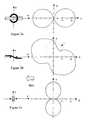
- Figure 1schematically represents a smart card according to the invention, in credit card format. This is the format more common, but the invention is, of course, applicable to smart cards and other electronic labels of very varied dimensions.
- the chip card showncomprises a pick-up coil 1 connected to a electronic circuit 2 comprising a memory and means for RF transmission at 125 kHz, frequency very generally used in this type of application.
- This type of circuitwell known to those skilled in the art, can be, for example, one of the circuits marketed by the company EM Marin (CH) under the references H 4000, 4001 to 4005 and 4050.
- the coil 1is crossed by an antenna 3 of high material magnetic permeability.
- This antennashould be very thin and have a particular shape. Thus, it can be carried out in a ribbon or a sheet metal with a high nickel content such as Mumétall® or Permalloy® which are said to have very high magnetic permeability. Found on the market for sheets 100 microns thick, or even 50 microns. This thin is necessary, on the one hand, so as not to increase by significantly the thickness of the card and, on the other hand, to reduce the eddy current losses in the antenna. Another possibility for further reducing these losses consists in making the antenna in a stack of even thinner sheets, e.g. 10 or 20 microns, isolated electrically between them like the sheets of a transformer.
- the coil 1, circuit 2 and antenna 3 assemblyis incorporated into the thickness of the body of the card 4, for example by overmolding of plastic material.
- the antenna 3has 3 zones, zone A which is in the plane of the face upper part of the coil, zone B which is in the plane of its lower face and zone C which is a connection zone between zones A and B.
- zone Awhich is in the plane of the face upper part of the coil
- zone Bwhich is in the plane of its lower face
- zone Cwhich is a connection zone between zones A and B.
- the extra thickness due to the antennais limited to the thicknesses of zones A and B which are superimposed on each side of the coil. For a thickness 50 micron antenna, so there is an extra thickness of 100 microns. We can easily play on the thickness of the coil to compensate for this extra thickness and keep the total thickness of the card inside the values standard.
- the antenna 3is diagonal. She is straight and, as its width is much less than the inside diameter of the coil 1, it can easily be slid inside. It is therefore made of single piece and area C is a simple folding that compensates for the height difference between parts A and B.
- the antennapractically does not pick up the flows perpendicular to the surface of the smart card, and its use is clearly associated with readers that generate stream lines parallel to the this surface.
- the antennaessentially allows concentrate the flow in the center of the card, in a small diameter coil, but does not solve the problem of dead positions.
- the present inventiontherefore represents an important improvement, mainly for "hands-free” applications, insofar as it largely solves this problem of dead positions.
- a conventional coil 1 of large diameteras shown in Figure 1
- the flows perpendicular to the surface of the card to chippass directly through the center of coil 1 without passing through antenna 3.
- equivalent diameterwe find characteristics equivalent to those of a conventional card without antenna. So by combining these two systems, antenna plus large diameter coil, we manage to do cross the coil as well by the flows parallel to the surface of the card, through the antenna 3, only through the flows perpendicular to this surface, directly through the large diameter coil 1, which done with the aim of eliminating dead positions, as it will appear better further.
- FIG. 1brepresents a card in which the antenna 3 is no longer in diagonal, but aligned along the longitudinal axis of the smart card. We arrive, indeed, to modify the response of the card in the different positions by changing the antenna configuration, which optimizes its depending on the applications. In the case of Figure 1b, the antenna is always in one piece. The characteristics of this card are given in figure 2.
- the antenna 3has a Z shape, more complex, to modify the characteristics, as shown in Figure 3. It may be easier to do in two parts.
- the upper part A and the lower part Boverlap in area C and are folded so that they overlap. They can be assembled by riveting, gluing or any other method. It is also possible, in certain cases, to have an antenna in two parts and leave an air gap between them, without affecting the good system operation.
- the voltage induced at 125 kHz across the pickup coil 1 with the Figure 1b antenna configurationis shown in Figure 2.
- the X axisis in the direction of the length of the card, the Y axis in the direction of the width and the Z axis perpendicular to the first two, or perpendicular to the surface from the menu.
- the voltageis represented vectorially as a function of the angle of rotation of the antenna assuming that it rotates along an axis perpendicular to the plane of the drawing.
- the thin linerepresents the tension obtained without antenna, and the thicker line the voltage obtained with the antenna in square.
- the starting position, corresponding to the angle of rotation 0,is shown on the left. Measurements are made inside a coil of Helmoltz supplied with constant current so as to have a uniform flow. The direction of this flow is horizontal, as indicated by the arrow.
- the X and Y axesare in the plane of the drawing and the card rotates along the Z axis.
- the coilis parallel to the flux lines on all of the 360 degrees of rotation. It is therefore not crossed by these flow lines if although, without antenna (dotted curve), the induced voltage is practically zero regardless of the angle.
- the flux passing through the antenna inside the coilis maximum at 0 and 180 degrees when the antenna is parallel to the flux lines. It is zero at 90 and 270 degrees when the antenna is perpendicular to the lines flow.
- the axes Z and Xare in the plane of the drawing and the card turns along the Y axis.
- the coilis parallel to the 0 and 180 degree flux lines. She is perpendicular to the flow lines at 90 and 270 degrees. Without antenna (dashed curve), the flux is zero in the first case and maximum in the second. So we have a sinusoidal distribution of the induced voltage in function of the angle, with passages at 0 and 180 degrees, and maximums at 90 and 270 degrees.
- the flux passing through the antenna inside the coilis maximum at 0 and 180 degrees when the antenna is parallel to the flux lines. It is zero at 90 and 270 degrees when the antenna is perpendicular to the lines flow. We can then see a very interesting phenomenon. A 0 and 180 degrees, the entire flux passing through the coil is brought by the antenna and we have the corresponding induced voltage. At 90 and 270 degrees, the antenna is inoperative, but we have the tension due to the direct passage of the flux through the coil, corresponding to the maximum voltage obtained when there is no antenna.
- the Z and Y axesare in the plane of the drawing and the card rotates along the X axis.
- the coilis parallel to the 0 and 180 degree flux lines. She is perpendicular to the flow lines at 90 and 270 degrees. Without antenna (dashed curve), the flux is zero in the first case and maximum in the second. So we have a sinusoidal distribution of the induced voltage in function of the angle, with passages at 0 and 180 degrees, and maximums at 90 and 270 degrees.
- the antennais practically inoperative at all angles, if although we find practically the same distribution of the induced voltage than without antenna. In this case, therefore, it is the use of a relatively large coil which is favorable, while the antenna does nothing.
- the voltage across the coilis proportional to the square of its diameter. With a small coil, we would have a tension negligible whatever the angle.
- it is necessary to dimension the pick-up coil with respect to the antennaso that the induced voltage across its terminals is of the same order of magnitude as the antenna either perpendicular or parallel to the flow lines.
Landscapes
- Engineering & Computer Science (AREA)
- Computer Hardware Design (AREA)
- Microelectronics & Electronic Packaging (AREA)
- Physics & Mathematics (AREA)
- General Physics & Mathematics (AREA)
- Theoretical Computer Science (AREA)
- Computer Networks & Wireless Communication (AREA)
- Credit Cards Or The Like (AREA)
- Near-Field Transmission Systems (AREA)
Abstract
Description
Translated fromFrenchLa présente invention concerne une carte à puce sans contact, de type RF(radio-fréquence).The present invention relates to a contactless smart card, of the RF type.(radio frequency).
De nombreuses exécutions de ce genre de carte sont disponibles sur lemarché. Elles comportent généralement un module électronique comprenantune bobine captrice associée à un circuit intégré, cette bobine permettant,d'une part, de transmettre les signaux RF et, d'autre part, de fournir l'énergienécessaire au fonctionnement du module électronique. Les documents US 4 155 091et EP 762 535 décrivent des exemples de telles réalisations.Many versions of this kind of card are available on themarket. They generally include an electronic module comprisinga sensing coil associated with an integrated circuit, this coil enabling,on the one hand, to transmit RF signals and, on the other hand, to supply energynecessary for the operation of the electronic module. US documents 4,155,091and EP 762 535 describe examples of such embodiments.
Les cartes les plus simples comportent uniquement un code que l'on peut lireà distance, mais on trouve également de plus en plus de cartes à puce àlecture/écriture comportant une mémoire de type EEPROM capable desauvegarder son information même en absence de source d'alimentation.L'écriture dans ces mémoires demande une énergie relativement importantequ'il est nécessaire de prélever aux bornes de la bobine captrice. Or cela peutposer des problèmes, particulièrement dans les systèmes d'accès "main libre"qui représentent l'une des applications majeures de telles cartes.The simplest cards only have a code that can be readremotely, but there are also more and more smart cardsread / write with an EEPROM type memory capable ofsave its information even in the absence of a power source.Writing in these memories requires a relatively large energythat it is necessary to take from the terminals of the pick-up coil. This cancause problems, particularly in hands-free access systemswhich represent one of the major applications of such cards.
Une solution pour obtenir l'énergie nécessaire au fonctionnement de la carteà la plus grande distance possible est d'utiliser une bobine de grande surfacepermettant de capter un maximum de flux. Ainsi, les bobines rondes ontsouvent un diamètre proche de la largeur de la carte et, dans certains cas, onutilise même des bobines rectangulaires qui couvrent pratiquement l'entier dela surface de celle-ci. Une autre possibilité consiste à intégrer dans la cartedes antennes en matériau à perméabilité élevée pour concentrer le fluxpassant à proximité de la carte au centre de la bobine captrice. Le documentWO 98/52141 décrit un tel système qui permet d'obteniravec des bobines de petit diamètre des performances équivalentes à cellesde bobines de grand diamètre.A solution to obtain the energy necessary for the operation of the cardat the greatest possible distance is to use a large surface coilallowing to capture a maximum of flow. So the round coils haveoften a diameter close to the width of the card and, in some cases,even uses rectangular coils that cover almost the entirethe surface of it. Another possibility is to integrate into the cardantennas made of high permeability material to concentrate the fluxpassing near the card in the center of the pick-up reel. The documentWO 98/52141 describes such a system which makes it possible to obtainwith coils of small diameter performances equivalent to thoselarge diameter coils.
Cependant, il subsiste un problème majeur. En effet, dans les deux casmentionnés, le flux maximum dans la bobine n'est obtenu que lorsque la cartea une orientation bien définie par rapport aux lignes de flux générées par le lecteur. Lorsqu' on modifie la position de la carte, le flux diminue rapidementet il y a même de nombreuses positions mortes où le flux dans la bobine esttout simplement nul ou, tout au moins, proche de zéro. Cela poseévidemment de graves problèmes, particulièrement dans le cadre desapplications "main libre" car la position de la carte relativement aux lignes deflux générées par le lecteur peut être très variable selon le porteur et l'endroitoù il a rangé sa carte.However, there remains a major problem. In fact, in both casesmentioned, the maximum flow in the coil is only obtained when the cardhas a well-defined orientation with respect to the flow lines generated by thereader. When you change the position of the map, the flow decreases quicklyand there are even many dead positions where the flux in the coil issimply zero or, at least, close to zero. That posesobviously serious problems, especially in the context of"hands-free" applications because the position of the card relative to the lines offlows generated by the reader can be very variable depending on the carrier and the locationwhere he put his card away.
La présente invention a précisément pour but de fournir une combinaisonbobine captrice/antenne permettant de résoudre en grande partie le problèmeévoqué ci-dessus en rendant la quantité de flux capté par la bobine beaucoupplus indépendant de la position entre la carte et les lignes de flux généréespar le lecteur.The object of the present invention is precisely to provide a combinationsensing coil / antenna to largely resolve the problemmentioned above by making the amount of flux picked up by the coil a lotmore independent of the position between the map and the generated flow linesby the reader.
De manière plus précise, l'invention concerne une carte à puce sans contact,de type RF, comportant une bobine captrice, un circuit électronique relié à labobine et des éléments en matériau de perméabilité magnétique élevéefaisant office d'antenne,comportent une première partie située sensiblement dans le plan de la facesupérieure de la bobine et une deuxième partie située sensiblement dans leplan de la face inférieure de la bobine. Elle est caractérisée par le fait que l'antenne comporte une partie de liaison entre lapremière et la deuxième partie, positionnée au centre de la bobine, cettedernière étant dimensionnée par rapport à l'antenne de manière que lestensions induites à ses bornes soient du même ordre de grandeur, quel'antenne soit parallèle ou perpendiculaire aux lignes de flux magnétiquegénérées par un dispositif de lecture.More specifically, the invention relates to a contactless smart card,RF type, comprising a pick-up coil, an electronic circuit connected to thecoil and elements made of high magnetic permeability materialacting as an antenna,have a first part located substantially in the plane of the faceupper part of the coil and a second part located substantially in theplane of the underside of the coil. It is characterized by the fact that the antenna includes a connecting part between thefirst and second part, positioned in the center of the spool, thislast being dimensioned with respect to the antenna so that theinduced voltages at its terminals are of the same order of magnitude, thatthe antenna is parallel or perpendicular to the magnetic flux linesgenerated by a reading device.
L'invention sera mieux comprise à la lecture de la description qui va suivre,donnée à titre explicatif et faite en regard des dessins annexés sur lesquels:
- les figures 1 a, b et c représentent quelques formes d'exécution d'unecarte à puce selon l'invention avec son antenne et sa bobine captrice;
- les figures 2 a, b et c représentent la tension aux bornes de la bobinecaptrice en fonction de la position de celle-ci dans le flux pour unepremière forme d'antenne; et
- les figures 3 a, b et c représentent la tension aux bornes de la bobinecaptrice en fonction de la position de celle-ci dans le flux pour unedeuxième forme d'antenne.
- Figures 1 a, b and c show some embodiments of a smart card according to the invention with its antenna and its pickup coil;
- Figures 2 a, b and c show the voltage across the pickup coil as a function of its position in the flux for a first form of antenna; and
- Figures 3 a, b and c show the voltage across the pickup coil as a function of its position in the flux for a second form of antenna.
On se référera tout d'abord à la figure 1 qui représente schématiquement unecarte à puce selon l'invention, au format carte de crédit. Il s'agit là du format leplus courant, mais l'invention est, bien sur, applicable à des cartes à puce etautres étiquettes électroniques de dimensions très variées.We will first refer to Figure 1 which schematically represents asmart card according to the invention, in credit card format. This is the formatmore common, but the invention is, of course, applicable to smart cards andother electronic labels of very varied dimensions.
La carte à puce représentée comporte une bobine captrice 1 reliée à uncircuit électronique 2 comportant une mémoire et des moyens detransmission RF à 125 kHz, fréquence très généralement utilisée dans cetype d'application. Ce type de circuit, bien connu de l'homme de métier, peutêtre, par exemple, l'un des circuits commercialisés par la société EM Marin(CH) sous les références H 4000, 4001 à 4005 et 4050.The chip card shown comprises a pick-
La bobine 1 est traversée par une antenne 3 en matériau à hauteperméabilité magnétique. Cette antenne doit être très mince et avoir uneforme particulière. Ainsi, elle peut être réalisée dans un ruban ou une feuillede métal à forte teneur en nickel comme le Mumétall® ou le Permalloy® quisont réputés avoir une perméabilité magnétique très élevée. On trouve sur lemarché des feuilles de 100 microns d'épaisseur, voire de 50 microns. Cettefaible épaisseur est nécessaire, d'une part, pour ne pas augmenter demanière significative l'épaisseur de la carte et, d'autre part, pour réduire lespertes par courant de Foucault dans l'antenne. Une autre possibilité pourdiminuer encore ces pertes consiste à réaliser l'antenne dans un empilage defeuilles encore plus minces, par exempte 10 ou 20 microns, isoléesélectriquement entre elles comme les tôles d'un transformateur.The
L'ensemble bobine 1, circuit 2 et antenne 3 est incorporé dans l'épaisseur ducorps de la carte 4, par exemple par surmoulage de matière plastique.The
L'antenne 3 comporte 3 zones, la zone A qui est dans le plan de la facesupérieure de la bobine, la zone B qui est dans le plan de sa face inférieure etla zone C qui est une zone de liaison entre les zones A et B. La surépaisseur due à l'antenne se limite aux épaisseurs des zones A et B qui sontsuperposées sur chacune des faces de la bobine. Pour une épaisseurd'antenne de 50 microns, on a donc une surépaisseur de 100 microns. Onpeut facilement jouer sur l'épaisseur de la bobine pour compenser cettesurépaisseur et maintenir l'épaisseur totale de la carte à l'intérieur des valeursstandard.The
Dans l'exemple de la figure 1a, l'antenne 3 est en diagonale. Elle est droite et,comme sa largeur est nettement inférieure au diamètre intérieur de la bobine1, elle peut facilement être glissée à l'intérieur. Elle est donc réalisée d'uneseule pièce et la zone C est un simple pliage qui permet de compenser ladifférence de hauteur entre les parties A et B.In the example of Figure 1a, the
En l'absence d'antenne, les flux magnétiques parallèles à la surface de lacarte à puce ne traversent pas la bobine 1 et ne génèrent donc aucunetension à ses bornes. Comme décrit dans le document WO 98/52 141,le fait d'incorporer l'antenne 3 à la carte permet de capter ces fluxmagnétiques parallèles à la surface de la carte, plus particulièrement ceux quisont dans l'axe de l'antenne. Ces flux vont passer de la zone A, soit de la facesupérieure de la bobine 1, vers la zone B, soit vers la face inférieure de celle-ci,ou inversement, en traversant le centre de la bobine 1 dans la zone C.Cela permet de générer aux bornes de la bobine 1 la tension nécessaire aubon fonctionnement du circuit électronique 2.In the absence of an antenna, magnetic fluxes parallel to the surface of thesmart card does not cross
Dans le brevet suisse susmentionné, l'antenne ne capte pratiquement pas lesflux perpendiculaires à la surface de la carte à puce, et son usage estclairement associé à des lecteurs qui génèrent des lignes de flux parallèles àla cette surface. Avec une telle stucture, l'antenne permet essentiellement deconcentrer le flux au centre de la carte, dans une bobine de petit diamètre,mais ne résout aucunement le problème des positions mortes.In the aforementioned Swiss patent, the antenna practically does not pick up theflows perpendicular to the surface of the smart card, and its use isclearly associated with readers that generate stream lines parallel tothe this surface. With such a structure, the antenna essentially allowsconcentrate the flow in the center of the card, in a small diameter coil,but does not solve the problem of dead positions.
La présente invention représente donc un perfectionnement important,principalement pour les applications "main libre", dans la mesure où ellepermet de résoudre en grande partie ce problème de positions mortes. Enassociant à l'antenne 3 une bobine 1 classique de grand diamètre, comme représenté à la figure 1, les flux perpendiculaires à la surface de la carte àpuce traversent directement le centre de la bobine 1 sans passer parl'antenne 3. A diamètre équivalent, on retrouve des caractéristiqueséquivalentes à celles d'une carte classique sans antenne. Ainsi, en combinantces deux systèmes, antenne plus bobine de grand diamètre, on arrive à fairetraverser la bobine aussi bien par les flux parallèles à la surface de la carte,par l'intermédiaire de l'antenne 3, que par les flux perpendiculaires à cettesurface, directement à travers la bobine 1 de grand diamètre, ce qui va tout àfait dans le but visé d'éliminer les positions mortes, comme il apparaítra mieuxplus loin.The present invention therefore represents an important improvement,mainly for "hands-free" applications, insofar as itlargely solves this problem of dead positions. Inassociating with antenna 3 a
La figure 1b représente une carte dans laquelle l'antenne 3 n'est plus endiagonale, mais alignée selon l'axe longitidinal de la carte à puce. On arrive,en effet, à modifier la réponse de la carte dans les différentes positions enchangeant la configuration de l'antenne, ce qui permet d'optimaliser sonfonctionnement en fonction des applications. Dans le cas de la figure 1b,l'antenne est toujours d'une seule pièce. Les caractéristiques de cette cartesont données à la figure 2.FIG. 1b represents a card in which the
A la figure 1c, au contraire, l'antenne 3 a une forme en Z, plus complexe,permettant de modifier les caractéristiques, comme représenté à la figure 3. Ilpeut être plus facile de la réaliser en deux parties. La partie supérieure A et lapartie inférieure B se recoupent dans la zone C et sont pliées de manière à sesuperposer. Elles peuvent être assemblées par rivetage, collage ou touteautre méthode. On peut également, dans certains cas, avoir une antenne endeux parties et laisser entre elles un entrefer, sans que cela nuise au bonfonctionnement du système.In FIG. 1c, on the contrary, the
La tension induite à 125 kHz aux bornes de la bobine captrice 1 avec laconfiguration d'antenne de la figure 1b est représentée à la figure 2. L'axe Xest dans le sens de la longueur de la carte, l'axe Y dans le sens de la largeuret l'axe Z perpendiculaire aux deux premiers, soit perpendiculaire à la surfacede la carte. La tension est représentée vectoriellement en fonction de l'anglede rotation de l'antenne en admettant que celle-ci tourne selon un axe perpendiculaire au plan du dessin. Le trait fin représente la tension obtenuesans antenne, et le trait plus épais la tension obtenue avec l'antenne enplace. La position de départ, correspondant à l'angle de rotation 0, estreprésentée à gauche. Les mesures sont faites à l'intérieur d'une bobine deHelmoltz alimentée à courant constant de manière à avoir un flux uniforme.La direction de ce flux est horizontale, comme l'indique la flèche.The voltage induced at 125 kHz across the
A la figure 2a, les axes X et Y sont dans le plan du dessin et la carte tourneselon l'axe Z. La bobine est parallèle aux lignes de flux sur l'ensemble des360 degrés de rotation. Elle n'est donc pas traversée par ces lignes de flux sibien que , sans antenne (courbe en pointillés), la tension induite estpratiquement nulle quel que soit l'angle.In Figure 2a, the X and Y axes are in the plane of the drawing and the card rotatesalong the Z axis. The coil is parallel to the flux lines on all of the360 degrees of rotation. It is therefore not crossed by these flow lines ifalthough, without antenna (dotted curve), the induced voltage ispractically zero regardless of the angle.
Avec l'antenne, le flux passant par l'antenne à l'intérieur de la bobine estmaximum à 0 et 180 degrés lorsque l'antenne est parallèle aux lignes de flux.Il est nul à 90 et 270 degrés lorsque l'antenne est perpendiculaire aux lignesde flux. On a donc une répartition sinusoïdale de la tension induite en fonctionde l'angle. Cette répartition avec antenne, même si elle présente deuxpassages par 0, est de toute manière beaucoup plus favorable que larépartition sans antenne.With the antenna, the flux passing through the antenna inside the coil ismaximum at 0 and 180 degrees when the antenna is parallel to the flux lines.It is zero at 90 and 270 degrees when the antenna is perpendicular to the linesflow. We therefore have a sinusoidal distribution of the induced voltage as a functionof the angle. This distribution with antenna, even if it has twopassages by 0, is in any case much more favorable than thedistribution without antenna.
A la figure 2b, les axes Z et X sont dans le plan du dessin et la carte tourneselon l'axe Y. La bobine est parallèle aux lignes de flux à 0 et 180 degrés. Elleest perpendiculaire aux lignes de flux à 90 et 270 degrés. Sans antenne(courbe en pointillés), le flux est nul dans le premier cas et maximum dans lesecond. On a donc une répartition sinusoïdale de la tension induite enfonction de l'angle, avec des passages à 0 et 180 degrés, et des maximum à90 et 270 degrés.In FIG. 2b, the axes Z and X are in the plane of the drawing and the card turnsalong the Y axis. The coil is parallel to the 0 and 180 degree flux lines. Sheis perpendicular to the flow lines at 90 and 270 degrees. Without antenna(dashed curve), the flux is zero in the first case and maximum in thesecond. So we have a sinusoidal distribution of the induced voltage infunction of the angle, with passages at 0 and 180 degrees, and maximums at90 and 270 degrees.
Avec l'antenne, le flux passant par l'antenne à l'intérieur de la bobine estmaximum à 0 et 180 degrés lorsque l'antenne est parallèle aux lignes de flux.Il est nul à 90 et 270 degrés lorsque l'antenne est perpendiculaire aux lignesde flux. On peut alors constater un phénomène très intéressant. A 0 et 180degrés, la totalité du flux traversant la bobine est amené par l'antenne et on ala tension induite correspondante. A 90 et 270 degrés, l'antenne est inopérante, mais on a la tension due au passage direct du flux à travers labobine, correspondant au maximum de tension obtenu lorsqu'il n'y a pasd'antenne. Dans les positions intermédiaires, par exemple à 60 et 240 degrés,les flux passant dans la bobine directement, d'une part, et par l'antenne,d'autre part, se contrarient, si bien que l'on a une certaine diminution de latension induite, sans qu'il y ait pourtant de passage à 0. Par contre, à 140 et330 degrés, ces flux s'additionnent, si bien que c'est là que l'on trouve lemaximum de tension induite.With the antenna, the flux passing through the antenna inside the coil ismaximum at 0 and 180 degrees when the antenna is parallel to the flux lines.It is zero at 90 and 270 degrees when the antenna is perpendicular to the linesflow. We can then see a very interesting phenomenon. A 0 and 180degrees, the entire flux passing through the coil is brought by the antenna and we havethe corresponding induced voltage. At 90 and 270 degrees, the antenna isinoperative, but we have the tension due to the direct passage of the flux through thecoil, corresponding to the maximum voltage obtained when there is noantenna. In the intermediate positions, for example at 60 and 240 degrees,the fluxes passing through the coil directly, on the one hand, and through the antenna,on the other hand, contradict each other so that there is a certain decrease in theinduced voltage, without however passing to 0. On the other hand, at 140 and330 degrees, these fluxes add up, so that's where we find themaximum induced voltage.
A la figure 2c, les axes Z et Y sont dans le plan du dessin et la carte tourneselon l'axe X. La bobine est parallèle aux lignes de flux à 0 et 180 degrés. Elleest perpendiculaire aux lignes de flux à 90 et 270 degrés. Sans antenne(courbe en pointillés), le flux est nul dans le premier cas et maximum dans lesecond. On a donc une répartition sinusoïdale de la tension induite enfonction de l'angle, avec des passages à 0 et 180 degrés, et des maximum à90 et 270 degrés.In Figure 2c, the Z and Y axes are in the plane of the drawing and the card rotatesalong the X axis. The coil is parallel to the 0 and 180 degree flux lines. Sheis perpendicular to the flow lines at 90 and 270 degrees. Without antenna(dashed curve), the flux is zero in the first case and maximum in thesecond. So we have a sinusoidal distribution of the induced voltage infunction of the angle, with passages at 0 and 180 degrees, and maximums at90 and 270 degrees.
Dans ce cas là, l'antenne est pratiquement inopérante dans tous les angles, sibien que l'on retrouve pratiquement la même répartition de la tension induiteque sans antenne. Dans ce cas, c'est donc l'utilisation d'une relativementgrande bobine qui est favorable, alors que l'antenne n'apporte rien. On noteraque, sans antenne, la tension aux bornes de la bobine est proportionnelle aucarré de son diamètre. Avec une petite bobine, on aurait une tensionnégligeable quel que soit l'angle. Pour avoir des performances similaires de lacarte à puce dans les principales directions, il est donc nécessaire dedimensionner la bobine captrice par rapport à l'antenne de manière que latension induite à ses bornes soit du même ordre de grandeur, que l'antennesoit perpendiculaire ou parrallèle aux lignes de flux.In this case, the antenna is practically inoperative at all angles, ifalthough we find practically the same distribution of the induced voltagethan without antenna. In this case, therefore, it is the use of a relativelylarge coil which is favorable, while the antenna does nothing. We will notethat, without antenna, the voltage across the coil is proportional to thesquare of its diameter. With a small coil, we would have a tensionnegligible whatever the angle. To have similar performances of thesmart card in the main directions, so it is necessary todimension the pick-up coil with respect to the antenna so that theinduced voltage across its terminals is of the same order of magnitude as the antennaeither perpendicular or parallel to the flow lines.
On voit ainsi clairement qu'en combinant, selon la présente invention, unebobine relativement grande qui capte les lignes de flux perpendiculaires à lacarte à puce non captées par l'antenne, alors que celle-ci capte les lignes deflux parallèles à la carte à puce que la bobine ne capte pas, on réalise cettecondition et on réduit de manière considérable les positions mortes, ce que l'on ne peut obtenir ni avec une bobine seule, même de grand diamètre, niavec une antenne associée à une petite bobine.It is thus clearly seen that by combining, according to the present invention, arelatively large coil which captures the flow lines perpendicular to thesmart card not picked up by the antenna, while the antenna picks up the lines offlows parallel to the smart card that the coil does not pick up, we realize thiscondition and the dead positions are considerably reduced, whichone cannot obtain neither with a single coil, even of large diameter, norwith an antenna associated with a small coil.
Sur la figure 3, on a représenté les mêmes courbes, mais avec une antenneen forme de Z . A la figure 3a, les axes X et Y sont dans le plan du dessin etla carte tourne selon l'axe Z. A la figure 3b, les axes Z et X sont dans le plandu dessin et la carte tourne selon l'axe Y. Enfin, à la figure 3c, les axes Z et Ysont dans le plan du dessin et la carte tourne selon l'axe X. Cetteconfiguration d'antenne en Z est particulièrement intéressante dans la mesureoù elle ne présente pratiquement pas de position morte quand on tourneselon l'axe Z (figure 3a). Quand on tourne selon les axes Y ou X (figures 3b et3c), le flux dans l'antenne est nul dans certaines positions, mais cela estcompensé par le flux qui traverse directement la bobine sans passer parl'antenne. On voit que l'on a donc une répartition très homogène de la tensioninduite dans les trois cas de figure, pratiquement sans passage à 0.In Figure 3, the same curves are shown, but with an antennaZ-shaped. In FIG. 3a, the axes X and Y are in the plane of the drawing andthe card rotates along the Z axis. In Figure 3b, the Z and X axes are in the planeof the drawing and the map rotates along the Y axis. Finally, in Figure 3c, the Z and Y axesare in the drawing plane and the map rotates along the X axis.Z antenna configuration is particularly interesting in the measurementwhere there is practically no dead position when we turnalong the Z axis (Figure 3a). When we turn along the Y or X axes (Figures 3b and3c), the flux in the antenna is zero in certain positions, but this iscompensated by the flux which directly crosses the coil without passing throughthe antenna. We see that we have a very homogeneous distribution of the tensioninduced in the three cases, practically without going to 0.
Il est donc possible d'adapter les caractéristiques de la carte à puce, et plusparticulièrement son comportement dans les différentes positions qu'ellepourrait avoir par rapport aux lignes de flux générées par le système delecture en adaptant la forme de l'antenne travaillant en association avec unebobine captrice de grand diamètre.It is therefore possible to adapt the characteristics of the smart card, and moreparticularly her behavior in the different positions shecould have compared to the flow lines generated by the systemreading by adapting the shape of the antenna working in association with alarge diameter pick-up coil.
Il existe, bien sûr, d'autres configurations possible de la carte à puce selon laprésente invention, mais leur description n'apporterait pas d'élémentsnouveaux pour la description de celle-ci.There are, of course, other possible configurations of the smart card depending on thepresent invention, but their description would not provide elementsnew for the description of it.
Claims (8)
- Contactless RF-type smart card, including a sensor coil (1), an electronic circuit(2) connected to said coil and an antenna (3) made of a material with high magneticpermeability, including a first part (A) located substantially in the plane of the upper coilsurface and a second part (B) located substantially in the plane of the lower coilsurface,characterised in that said antenna (3) includes a connecting part (C) betweenthe first and second parts located at the centre of the coil, the latter being dimensionedrelative to the antenna (3) such that the voltages induced across its terminals are ofthe same order of magnitude, whether the antenna is parallel or perpendicular to thelines of flux generated by a reader.
- Smart card according to claim 1,characterised in that the antenna (3) is madein a thin sheet or strip of metal with high magnetic permeability.
- Smart card according to claim 1,characterised in that the antenna (3) is madeof a metal with a high nickel content.
- Smart card according to claim 1,characterised in that the antenna (3) is madein a single piece, the connecting part (C) consisting of a fold passing through thecentre of the coil (1).
- Smart card according to claim 1,characterised in that the antenna (3) is madein two parts, the first (A) and the second (B) parts overlapping each other at the centreof the coil (1) in the connecting part (C).
- Smart card according to claim 1,characterised in that the antenna (3) isstraight.
- Smart card according to claim 1,characterised in that the antenna (3) is placeddiagonally.
- Smart card according to claim 1,characterised in that the antenna (3) is Z-shaped.
Applications Claiming Priority (3)
| Application Number | Priority Date | Filing Date | Title |
|---|---|---|---|
| CH00867/99ACH693394A5 (en) | 1999-05-07 | 1999-05-07 | chip card comprising an antenna. |
| CH86799 | 1999-05-07 | ||
| PCT/CH2000/000242WO2000069016A1 (en) | 1999-05-07 | 2000-05-03 | Chip card comprising an antenna |
Publications (2)
| Publication Number | Publication Date |
|---|---|
| EP1177597A1 EP1177597A1 (en) | 2002-02-06 |
| EP1177597B1true EP1177597B1 (en) | 2003-07-09 |
Family
ID=4197034
Family Applications (1)
| Application Number | Title | Priority Date | Filing Date |
|---|---|---|---|
| EP00918651AExpired - LifetimeEP1177597B1 (en) | 1999-05-07 | 2000-05-03 | Chip card comprising an antenna |
Country Status (5)
| Country | Link |
|---|---|
| US (1) | US6644555B1 (en) |
| EP (1) | EP1177597B1 (en) |
| CH (1) | CH693394A5 (en) |
| DE (1) | DE60003811T2 (en) |
| WO (1) | WO2000069016A1 (en) |
Cited By (2)
| Publication number | Priority date | Publication date | Assignee | Title |
|---|---|---|---|---|
| US7190319B2 (en) | 2001-10-29 | 2007-03-13 | Forster Ian J | Wave antenna wireless communication device and method |
| US7345643B2 (en) | 2001-10-29 | 2008-03-18 | Mineral Lassen Llc | Wave antenna wireless communication device and method |
Families Citing this family (16)
| Publication number | Priority date | Publication date | Assignee | Title |
|---|---|---|---|---|
| TW531976B (en)* | 2001-01-11 | 2003-05-11 | Hanex Co Ltd | Communication apparatus and installing structure, manufacturing method and communication method |
| US6630910B2 (en) | 2001-10-29 | 2003-10-07 | Marconi Communications Inc. | Wave antenna wireless communication device and method |
| JP4367013B2 (en)* | 2002-10-28 | 2009-11-18 | セイコーエプソン株式会社 | Non-contact communication medium |
| US20050237241A1 (en)* | 2004-04-27 | 2005-10-27 | Garber Richard S | Antenna for radio frequency identification reader |
| US20060118639A1 (en)* | 2004-12-06 | 2006-06-08 | First Data Corporation | Punchout contactless transaction card |
| JP2006235825A (en)* | 2005-02-23 | 2006-09-07 | Omron Corp | Broadband ic tag |
| US7061769B1 (en)* | 2005-03-11 | 2006-06-13 | Jung-Che Chang | USB/OTG-interface storage card |
| EP1892794A4 (en)* | 2005-06-14 | 2010-07-14 | Murata Manufacturing Co | Coil antenna structure and portable electronic apparatus |
| JP4414940B2 (en) | 2005-06-14 | 2010-02-17 | ソニーケミカル&インフォメーションデバイス株式会社 | ANTENNA DEVICE AND ANTENNA DEVICE ADJUSTING METHOD |
| FR2891091B1 (en)* | 2005-09-22 | 2008-01-11 | Commissariat Energie Atomique | OMNIDIRECTIONAL PLANAR ANTENNA AND METHOD OF MANUFACTURE |
| US7991692B2 (en) | 2006-10-09 | 2011-08-02 | First Data Corporation | Electronic payment instrument and packaging |
| TWI345856B (en)* | 2007-09-14 | 2011-07-21 | Arcadyan Technology Corp | Dual band antenna |
| US7885878B2 (en) | 2008-05-28 | 2011-02-08 | First Data Corporation | Systems and methods of payment account activation |
| TWI483471B (en) | 2011-08-02 | 2015-05-01 | Arcadyan Technology Corp | Dual band antenna |
| JP6287271B2 (en)* | 2014-01-31 | 2018-03-07 | 株式会社村田製作所 | 3-axis antenna |
| JP6179543B2 (en)* | 2014-05-13 | 2017-08-16 | 株式会社村田製作所 | 3-axis antenna |
Family Cites Families (4)
| Publication number | Priority date | Publication date | Assignee | Title |
|---|---|---|---|---|
| US4155091A (en)* | 1977-09-12 | 1979-05-15 | Iec Electronics Corporation | Compact omnidirectional antenna array |
| FR2714988B1 (en)* | 1994-01-11 | 1996-03-29 | Gemplus Card Int | System for the contactless identification of objects, in particular metallic objects. |
| KR100459839B1 (en)* | 1995-08-22 | 2005-02-07 | 미쓰비시 마테리알 가부시키가이샤 | Antennas and transponders for transponders |
| FR2776797B1 (en)* | 1998-03-30 | 2000-06-30 | Gemplus Card Int | CONTACTLESS INTEGRATED CIRCUIT CARD WITH MEANS OF INHIBITION |
- 1999
- 1999-05-07CHCH00867/99Apatent/CH693394A5/ennot_activeIP Right Cessation
- 2000
- 2000-05-03DEDE60003811Tpatent/DE60003811T2/ennot_activeExpired - Fee Related
- 2000-05-03WOPCT/CH2000/000242patent/WO2000069016A1/enactiveIP Right Grant
- 2000-05-03USUS10/031,648patent/US6644555B1/ennot_activeExpired - Lifetime
- 2000-05-03EPEP00918651Apatent/EP1177597B1/ennot_activeExpired - Lifetime
Cited By (5)
| Publication number | Priority date | Publication date | Assignee | Title |
|---|---|---|---|---|
| US7190319B2 (en) | 2001-10-29 | 2007-03-13 | Forster Ian J | Wave antenna wireless communication device and method |
| US7345643B2 (en) | 2001-10-29 | 2008-03-18 | Mineral Lassen Llc | Wave antenna wireless communication device and method |
| US7373713B2 (en) | 2001-10-29 | 2008-05-20 | Mineral Lassen Llc | Wave antenna wireless communication device and method |
| US7420520B2 (en) | 2001-10-29 | 2008-09-02 | Mineral Lassen Llc | Wave antenna wireless communication device and method |
| US7439928B2 (en) | 2001-10-29 | 2008-10-21 | Mineral Lassen Llc | Wave antenna wireless communication device and method |
Also Published As
| Publication number | Publication date |
|---|---|
| CH693394A5 (en) | 2003-07-15 |
| EP1177597A1 (en) | 2002-02-06 |
| WO2000069016A1 (en) | 2000-11-16 |
| US6644555B1 (en) | 2003-11-11 |
| DE60003811D1 (en) | 2003-08-14 |
| DE60003811T2 (en) | 2004-06-03 |
Similar Documents
| Publication | Publication Date | Title |
|---|---|---|
| EP1177597B1 (en) | Chip card comprising an antenna | |
| EP0980562B1 (en) | Contactless chip card associated with rf transmission means | |
| EP1118960B1 (en) | Contactless electronic module for a card or a label | |
| FR2919409A1 (en) | SECURE DOCUMENT WITH NON-CONTACT CHIP WITH DATA PROTECTION AGAINST UNAUTHORIZED READING. | |
| EP1275082B1 (en) | Electronic label | |
| WO2005078649A1 (en) | Passive transmitter receiver device fed by an electromagnetic wave | |
| EP1883996A2 (en) | Electronic entity with magnetic antenna | |
| FR2963696A1 (en) | MICROCIRCUIT DEVICE COMPRISING NEAR FIELD COMMUNICATION ANTENNA CIRCUIT | |
| WO2016009142A1 (en) | Electronic entity having an rfid transponder | |
| EP0642181B1 (en) | Magnetoresistive device and sensor with a geometric repetitive pattern | |
| WO1997034249A1 (en) | Device for contactless data exchange with an electronic ticket | |
| EP3794507B1 (en) | Electronic passport secured against unauthorised reading | |
| CA2646813A1 (en) | Radiofrequency device | |
| FR2610754A1 (en) | DATA EXCHANGE TRANSDUCER FOR INTEGRATED CIRCUIT BOARD | |
| WO2007057467A1 (en) | Method of producing a contactless transponder by stitching the contactless module to an antenna, and transponder obtained | |
| EP2966597A1 (en) | Frequency tuning of an electronic label | |
| EP3391461B1 (en) | Wireless communication module, plate suitable for use in manufacturing said module and method for manufacturing said module | |
| EP0960387B1 (en) | Rf label comprising an integrated circuit associated with highly permeable elements | |
| WO2007054631A1 (en) | Smart card provided with an advantageously interdigital capacitor | |
| FR3132581A1 (en) | Contactless communication device | |
| FR2983325A1 (en) | Method for cutting data carrier card e.g. subscriber identity module, for mobile phone, involves moving cutting surface in direction perpendicular to planar structure, and bringing cutting surface in contact with arcuate structure | |
| FR2944367A1 (en) | Thin film type battery for e.g. dual smart card, has end face provided with extension forming deformable tabs extending from body, where tabs are arranged in offset position with respect to each other along peripheral sidewall of body |
Legal Events
| Date | Code | Title | Description |
|---|---|---|---|
| PUAI | Public reference made under article 153(3) epc to a published international application that has entered the european phase | Free format text:ORIGINAL CODE: 0009012 | |
| 17P | Request for examination filed | Effective date:20011121 | |
| AK | Designated contracting states | Kind code of ref document:A1 Designated state(s):AT BE CH CY DE DK ES FI FR GB GR IE IT LI LU MC NL PT SE | |
| GRAH | Despatch of communication of intention to grant a patent | Free format text:ORIGINAL CODE: EPIDOS IGRA | |
| GRAH | Despatch of communication of intention to grant a patent | Free format text:ORIGINAL CODE: EPIDOS IGRA | |
| GRAA | (expected) grant | Free format text:ORIGINAL CODE: 0009210 | |
| AK | Designated contracting states | Designated state(s):DE FR GB IT | |
| REG | Reference to a national code | Ref country code:GB Ref legal event code:FG4D Free format text:NOT ENGLISH | |
| REF | Corresponds to: | Ref document number:60003811 Country of ref document:DE Date of ref document:20030814 Kind code of ref document:P | |
| REG | Reference to a national code | Ref country code:IE Ref legal event code:FG4D Free format text:FRENCH | |
| GBT | Gb: translation of ep patent filed (gb section 77(6)(a)/1977) | Effective date:20031110 | |
| REG | Reference to a national code | Ref country code:IE Ref legal event code:FD4D | |
| PGFP | Annual fee paid to national office [announced via postgrant information from national office to epo] | Ref country code:GB Payment date:20040420 Year of fee payment:5 | |
| PLBE | No opposition filed within time limit | Free format text:ORIGINAL CODE: 0009261 | |
| STAA | Information on the status of an ep patent application or granted ep patent | Free format text:STATUS: NO OPPOSITION FILED WITHIN TIME LIMIT | |
| 26N | No opposition filed | Effective date:20040414 | |
| PG25 | Lapsed in a contracting state [announced via postgrant information from national office to epo] | Ref country code:DE Free format text:LAPSE BECAUSE OF NON-PAYMENT OF DUE FEES Effective date:20041201 | |
| PG25 | Lapsed in a contracting state [announced via postgrant information from national office to epo] | Ref country code:FR Free format text:LAPSE BECAUSE OF NON-PAYMENT OF DUE FEES Effective date:20050131 | |
| REG | Reference to a national code | Ref country code:FR Ref legal event code:ST | |
| PG25 | Lapsed in a contracting state [announced via postgrant information from national office to epo] | Ref country code:IT Free format text:LAPSE BECAUSE OF NON-PAYMENT OF DUE FEES Effective date:20050503 Ref country code:GB Free format text:LAPSE BECAUSE OF NON-PAYMENT OF DUE FEES Effective date:20050503 | |
| GBPC | Gb: european patent ceased through non-payment of renewal fee | Effective date:20050503 |