EP1172962A2 - Bit rate agile clock recovery circuit - Google Patents
Bit rate agile clock recovery circuitDownload PDFInfo
- Publication number
- EP1172962A2 EP1172962A2EP01305957AEP01305957AEP1172962A2EP 1172962 A2EP1172962 A2EP 1172962A2EP 01305957 AEP01305957 AEP 01305957AEP 01305957 AEP01305957 AEP 01305957AEP 1172962 A2EP1172962 A2EP 1172962A2
- Authority
- EP
- European Patent Office
- Prior art keywords
- clock
- phase
- pair
- input
- clock signals
- Prior art date
- Legal status (The legal status is an assumption and is not a legal conclusion. Google has not performed a legal analysis and makes no representation as to the accuracy of the status listed.)
- Withdrawn
Links
- 238000011084recoveryMethods0.000titleclaimsabstractdescription20
- 230000007704transitionEffects0.000claimsabstractdescription19
- 238000000034methodMethods0.000claimsdescription6
- 238000005070samplingMethods0.000claimsdescription6
- 239000013643reference controlSubstances0.000claimsdescription4
- 238000010586diagramMethods0.000description5
- 230000005540biological transmissionEffects0.000description4
- 230000001960triggered effectEffects0.000description3
- RGNPBRKPHBKNKX-UHFFFAOYSA-NhexaflumuronChemical compoundC1=C(Cl)C(OC(F)(F)C(F)F)=C(Cl)C=C1NC(=O)NC(=O)C1=C(F)C=CC=C1FRGNPBRKPHBKNKX-UHFFFAOYSA-N0.000description2
- 238000000819phase cycleMethods0.000description2
- 230000035559beat frequencyEffects0.000description1
- 238000009432framingMethods0.000description1
- 230000003287optical effectEffects0.000description1
- 230000036961partial effectEffects0.000description1
Images

Classifications
- H—ELECTRICITY
- H04—ELECTRIC COMMUNICATION TECHNIQUE
- H04L—TRANSMISSION OF DIGITAL INFORMATION, e.g. TELEGRAPHIC COMMUNICATION
- H04L7/00—Arrangements for synchronising receiver with transmitter
- H04L7/02—Speed or phase control by the received code signals, the signals containing no special synchronisation information
- H04L7/033—Speed or phase control by the received code signals, the signals containing no special synchronisation information using the transitions of the received signal to control the phase of the synchronising-signal-generating means, e.g. using a phase-locked loop
- H04L7/0337—Selecting between two or more discretely delayed clocks or selecting between two or more discretely delayed received code signals
- H04L7/0338—Selecting between two or more discretely delayed clocks or selecting between two or more discretely delayed received code signals the correction of the phase error being performed by a feed forward loop
- H—ELECTRICITY
- H03—ELECTRONIC CIRCUITRY
- H03L—AUTOMATIC CONTROL, STARTING, SYNCHRONISATION OR STABILISATION OF GENERATORS OF ELECTRONIC OSCILLATIONS OR PULSES
- H03L7/00—Automatic control of frequency or phase; Synchronisation
- H03L7/06—Automatic control of frequency or phase; Synchronisation using a reference signal applied to a frequency- or phase-locked loop
- H03L7/08—Details of the phase-locked loop
- H03L7/099—Details of the phase-locked loop concerning mainly the controlled oscillator of the loop
- H03L7/0995—Details of the phase-locked loop concerning mainly the controlled oscillator of the loop the oscillator comprising a ring oscillator
- H03L7/0996—Selecting a signal among the plurality of phase-shifted signals produced by the ring oscillator
Definitions
- the present inventionrelates to the recovery of clock information from a digital data signal, and more particularly to a bit rate agile clock recovery circuit that performs instant lock-on clock recovery without glitches.
- the Banu/Dunlop proposed methoduses three matched gated voltage controlled oscillators, with two of the oscillators being zero-phase-started and stopped alternately by data transitions and the third allowed to run continuously.
- the output of the third oscillatoris fed into a conventional charge-pumped PLL and phase locked to a local reference signal. Since the same control voltage is applied to all three oscillators, the output frequencies of the first two are in precise relationships to the reference frequency for all process and temperature conditions within a small but finite matching error.
- This indirect frequency tuning techniqueoperates continuously and is not affected by the on/off state of the first two oscillators at any particular time. Combining continuous frequency tuning with data-transition-triggered zero-phase start is sufficient to reconstruct the clock instantaneously.
- phase errors that accumulate between transitions of the first two oscillators due to their frequency mismatches to the actual data rateare discarded every time the oscillators are stopped.
- the open-loop nature of this techniqueprovides great locking agility, but the clock inherits all the timing errors of the data transitions, such as input signal duty-cycle distortion.
- An optional divide-by-twomay be used to insure that the oscillators are triggered only by up or down transitions at the expense of effectively halving the input transition density.
- a more serious data timing erroris due to phase noise or jitter.
- An elastic storemay be added to the clock recovery circuit, the noisy data being input to a FIFO and read out by a clean local clock.
- Banu/Dunlop approachrequires that two oscillators match in frequency roughly within 1/2000, depending upon the data transmission protocol. This requirement has to be met while the two oscillators are tuned over a frequency range of 1.5-3 GHz for current high-speed transmission systems, especially those carrying baseband high definition television data.
- the present inventionprovides a bit rate agile clock recovery circuit that generates from a VCO and PLL combination a pair of quadrature phase clock signals at approximately the frequency of an input digital data signal, the frequency being determined by a reference control signal input to the PLL.
- the quadrature phase clock signalsare not phase locked to the input digital data signal.
- a clock phase select circuithas as inputs the pair of quadrature phase clock signals and a code generated from the pair of quadrature phase clock signals by the transitions in the input digital data signal. Based upon the code the clock phase select circuit selects one of four phases of the VCO clock frequency as the regenerated clock that is then used to extract the data from the input digital data signal.
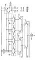
- Fig. 1is a block diagram view of a bit rate agile clock recovery circuit according to the present invention.
- Fig. 2is a block diagram view of a flip-flop triggered on both clock edges for the bit agile clock recovery circuit according to the present invention.
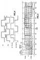
- Fig. 3is a circuit diagram view of a clock phase select circuit for the bit rate agile clock recovery circuit according to the present invention.
- Fig. 4is a waveform diagram view illustrating the transition between phases of the VCO clock frequency for the bit rate agile clock recovery circuit according to the present invention.
- Fig. 5is a waveform diagram view of various waveforms associated with the bit rate agile clock recover circuit according to the present invention.
- a phase locked loop (PLL) 12is used to control the frequency of a tunable voltage controlled oscillator (VCO) 14.
- the frequency of the VCO 14is determined by a reference control signal input to the PLL 12.
- the VCO 14may be a two stage ring oscillator.
- the outputs from the VCO 14are a pair of differential clock signals P1, P2 in quadrature phase which are input to a clock phase select circuit 16.
- the quadrature phase clock signalsare not phase locked to the input digital data signal, but are set to the approximate frequency expected for the input digital data signal.
- the pair of differential clock signals P1, P2also are input to respective flip-flops 18, 20 at the data input terminals.
- An input digital data signalis input to the clock input terminals of the flip-flops 18, 20.
- the pair of differential clock signals P1, P2are inverted by the clock phase select circuit 16 so that there exist two additional pairs of differential clock signals P3, P4 for selecting from.
- the Q outputs from the flip-flops 18, 20are input to the clock phase select circuit 16 which selects one of the four pairs of differential signals P1, P2, P3, P4 as an output clock signal C based upon the outputs from the flip-flops.
- the output clock signal Cclocks another flip-flop 22 to which the input digital data signal is input at the data input terminal to recover the data D.
- a delay at the data input of the data flip-flop 22may be used to assure that clock phase selection is not changed just as the input is changing.
- the two pairs of quadrature clock outputs P1, P2 from the VCO 14are sampled by the two flip-flops 18, 20 on transitions of the input digital data signal.
- the samplesare held as Q1, Q2.
- the flip-flopsmay be clocked on both positive and negative edges to extract all available timing information from the input digital data signal.
- Such a flip-flopis shown in Fig. 2 having a pair of latches 24, 26 to which the quadrature clock signals P1,P2 are applied and an inverter 28 coupled to the clock input of one of the two latches, with the input data being applied to the input of the inverter and to the clock input of the other of the two latches.
- the outputs of the two latches 24, 26are applied as inputs to an output multiplexer 30 , to which the input data signal is applied as a select signal. Therefore on positive transitions of the input data signal the value of the clock signal is latched in one latch and on negative transitions the value of the clock signal is latched in the other latched. Simultaneously the output of one latch is output by the multiplexer while the other latch is being loaded.
- the samples Q1, Q2define how the input signal phase is related to the clock phases P1, P2, P3, P4 as illustrated by the waveform in Fig. 1.
- the "1"s and “0"s on the P1 and P2 waveformsare the values of Q1 and Q2 when sampled during that time.
- the clock phase select circuit 16uses the Q1, Q2 values to select the clock phase P1-P4 which fits the timing of the input data transition best. That phase is output as clock C .
- the VCO 14is perfectly matched in frequency to the input signal clock frequency, the selected phase from the clock phase select circuit 16 does not change.
- the selected phasecycles 1-4 over and over again, either backwards or forwards, at the beat frequency of the two clocks. Therefore the VCO frequency should match the input signal clock frequency well enough so that it drifts less than one phase, i.e., one quarter cycle, in the longest period of no transitions in the input data signal.
- SONET OC-48this is the 384 bits still unscrambled immediately following the A1, A2 framing signal.
- the VCO frequencyneeds to match the input data signal frequency better than 1/1546, or about 500 ppm.
- the clock phase select circuit 16is shown in greater detail in Fig. 3. This circuit is designed to interpolate between adjacent phases if there is metastability in either Q1 or Q2 in order to make it "metastable proof.” If there is metastability in either of the sampling flip-flops 18, 20, partials of two adjacent phases of the recovered clock which add to one are chosen. When there is a clock phase change, the circuit is designed to change during a time when the old phase and new phase are equal, as shown in Fig. 4, to avoid generating glitches. This circuit has four phase differential transistor circuits 32, 34, 36, 38 to which clock phase pairs P1, P3 and P2, P4 are applied, with two of the circuits being reversed from the other two.
- a cascade of drive differential transistor circuits 40, 42, 44are configured to receive the Q1, Q2 samples, and the entire cascade of transistor circuits 32-44 is driven by a current source 46.
- the single current source 46 at the bottom of the cascade of transistor circuits 32-44insures that two adjacent clock phases are partially selected with a total sum of one if there is metastability in either sampling flip-flop 18, 20.
- the outputs from the collectors of the phase differential transistor circuits 32-38are coupled to an output differential emitter follower transistor circuit 48 to provide the selected phase clock output C.
- the VCO control voltageis shown at a negative value for the first five nanoseconds and positive for the next five nanoseconds. This indicates that the VCO frequency is too low for the first five nanoseconds and too high for the next five nanoseconds.
- the first phase select bit Q1is negative until about 1.7 nanoseconds and then goes positive until about 5.3 nanoseconds, returns to positive at about 5.7 nanoseconds until about 9.3 nanoseconds.
- the second phase select bit Q2is negative until about 3.7 nanoseconds, and returns negative at about 7.3 nanoseconds. Therefore until 1.7 nanoseconds P3 is the selected clock phase output C, at which point P4 is selected.
- the bit rate agile clock recovery circuit described abovemay be built almost entirely from standard digital building blocks, except for the tunable voltage controlled oscillator 12 which of necessity has a tunable analog feature.
- the jitter of the recovered clock Chas a peak-to-peak value of 0.25 unit intervals (UI), which is the time allocated to each bit, due to the phase select circuit 16. Since the clock C is used only internally to recover the data from the input digital data signal, this jitter is not of concern.
- the present inventionprovides a bit rate agile clock recovery circuit by generating a pair of quadrature clock signals from a VCO and PLL combination, and selecting one of four clock phases to use based upon the phase of the quadrature clock signals when the input data transitions.
Landscapes
- Engineering & Computer Science (AREA)
- Computer Networks & Wireless Communication (AREA)
- Signal Processing (AREA)
- Stabilization Of Oscillater, Synchronisation, Frequency Synthesizers (AREA)
- Synchronisation In Digital Transmission Systems (AREA)
- Manipulation Of Pulses (AREA)
Abstract
Description
The present invention relates to the recovery of clock information froma digital data signal, and more particularly to a bit rate agile clock recoverycircuit that performs instant lock-on clock recovery without glitches.
Traditional narrow-band clock recovery circuits, such as those basedon LC tanks, SAW filters or phase locked loops (PLLs), suffer from thefundamental limitation of locking, i.e., reaching steady-state operation slowlycompared to an input data rate. This is inconsequential in classical digitallinks where phase-coherent data flows continuously. However if data arrivesin asynchronous packets as in modern telecommunication systems such aspassive optical networks, long locking times cause significant problems intransmission efficiency.
The early solutions for fast-locking clock recovery were based onanalog PLLs (see "A Single Chip NMOS Ethernet Controller" by A.G. Bell andG. Borriello, Digest of Technical Papers, IEEE ISSCC, pp. 70-71, February1983), but these circuits still required small preambles, typically 5-15 bits,and/or bandwidth-wasting line coding, such as Manchester coding. Adifferent integrated solution is provided by an over-sampled analog/digitalapproach (see "A 30 MHz High-Speed Analog/Digital PLL in 2 µm CMOS" byB. Kim, D.N. Helman and R.R. Gray, Digest of Technical Papers, IEEEISSCC, pp. 104-105, February 1990). These circuits may be designed towork with non-return to zero (NRZ) data and with very small or no preambles. However due to the significant amount of fast digital circuitry required and tosubtle problems, such as latch metastability, this approach is very difficult athigh frequencies in the gigahertz range. Also the resulting circuits tend to belarge and to dissipate large amounts of power. The clock recovery methodproposed by M. Banu and A.E. Dunlop, "660 Mb/s CMOS Clock RecoveryCircuit with Instantaneous Locking", Electronics Letters, Vol. 28, No. 23, pp.2127-2130, November 5, 1992, avoids most of these problems inherently.Lock is accomplished instantaneously on the first data transition without over-samplingand is suitable for low-power and/or high-frequency operation.
The Banu/Dunlop proposed method uses three matched gated voltagecontrolled oscillators, with two of the oscillators being zero-phase-started andstopped alternately by data transitions and the third allowed to runcontinuously. The output of the third oscillator is fed into a conventionalcharge-pumped PLL and phase locked to a local reference signal. Since thesame control voltage is applied to all three oscillators, the output frequenciesof the first two are in precise relationships to the reference frequency for allprocess and temperature conditions within a small but finite matching error.This indirect frequency tuning technique operates continuously and is notaffected by the on/off state of the first two oscillators at any particular time.Combining continuous frequency tuning with data-transition-triggered zero-phasestart is sufficient to reconstruct the clock instantaneously. The phaseerrors that accumulate between transitions of the first two oscillators due totheir frequency mismatches to the actual data rate are discarded every timethe oscillators are stopped. The open-loop nature of this technique provides great locking agility, but the clock inherits all the timing errors of the datatransitions, such as input signal duty-cycle distortion. An optional divide-by-twomay be used to insure that the oscillators are triggered only by up ordown transitions at the expense of effectively halving the input transitiondensity. A more serious data timing error is due to phase noise or jitter. Anelastic store may be added to the clock recovery circuit, the noisy data beinginput to a FIFO and read out by a clean local clock.
The Banu/Dunlop approach requires that two oscillators match infrequency roughly within 1/2000, depending upon the data transmissionprotocol. This requirement has to be met while the two oscillators are tunedover a frequency range of 1.5-3 GHz for current high-speed transmissionsystems, especially those carrying baseband high definition television data.
What is desired is a bit rate agile instantaneous clock recovery circuitfor gigahertz data transmission systems that is relatively simple and providesclock transitions without glitches.
Accordingly the present invention provides a bit rate agile clockrecovery circuit that generates from a VCO and PLL combination a pair ofquadrature phase clock signals at approximately the frequency of an inputdigital data signal, the frequency being determined by a reference controlsignal input to the PLL. The quadrature phase clock signals are not phaselocked to the input digital data signal. A clock phase select circuit has asinputs the pair of quadrature phase clock signals and a code generated from the pair of quadrature phase clock signals by the transitions in the inputdigital data signal. Based upon the code the clock phase select circuitselects one of four phases of the VCO clock frequency as the regeneratedclock that is then used to extract the data from the input digital data signal.
The objects, advantages and other novel features are apparent fromthe following detailed description when read in conjunction with the appendedclaims and attached drawing.
Fig. 1 is a block diagram view of a bit rate agile clock recovery circuitaccording to the present invention.
Fig. 2 is a block diagram view of a flip-flop triggered on both clockedges for the bit agile clock recovery circuit according to the presentinvention.
Fig. 3 is a circuit diagram view of a clock phase select circuit for the bitrate agile clock recovery circuit according to the present invention.
Fig. 4 is a waveform diagram view illustrating the transition betweenphases of the VCO clock frequency for the bit rate agile clock recovery circuitaccording to the present invention.
Fig. 5 is a waveform diagram view of various waveforms associatedwith the bit rate agile clock recover circuit according to the present invention.
Referring now to Fig. 1 a phase locked loop (PLL)12 is used to controlthe frequency of a tunable voltage controlled oscillator (VCO)14. Thefrequency of theVCO 14 is determined by a reference control signal input tothePLL 12. The VCO14 may be a two stage ring oscillator. The outputsfrom theVCO 14 are a pair of differential clock signalsP1, P2 in quadraturephase which are input to a clock phaseselect circuit 16. The quadraturephase clock signals are not phase locked to the input digital data signal, butare set to the approximate frequency expected for the input digital datasignal. The pair of differential clock signalsP1, P2 also are input torespective flip-flops flops select circuit 16 so that there exist two additional pairs of differential clock signalsP3, P4for selecting from. The Q outputs from the flip-flops select circuit 16 which selects one of the four pairs of differentialsignalsP1, P2, P3, P4 as an output clock signalC based upon the outputsfrom the flip-flops. The output clock signalC clocks another flip-flop 22 towhich the input digital data signal is input at the data input terminal to recoverthe dataD. A delay at the data input of the data flip-flop 22 may be used toassure that clock phase selection is not changed just as the input ischanging.
In operation the two pairs of quadrature clock outputsP1, P2 from theVCO 14 are sampled by the two flip-flops latches inverter 28 coupled to the clock input of one of the twolatches, with the input data being applied to the input of the inverter and tothe clock input of the other of the two latches. The outputs of the twolatches output multiplexer 30, to which the inputdata signal is applied as a select signal. Therefore on positive transitions ofthe input data signal the value of the clock signal is latched in one latch andon negative transitions the value of the clock signal is latched in the otherlatched. Simultaneously the output of one latch is output by the multiplexerwhile the other latch is being loaded.
The samplesQ1, Q2 define how the input signal phase is related tothe clock phasesP1, P2, P3, P4 as illustrated by the waveform in Fig. 1. The"1"s and "0"s on theP1 andP2 waveforms are the values ofQ1 andQ2 whensampled during that time. The clock phaseselect circuit 16 uses theQ1, Q2values to select the clock phaseP1-P4 which fits the timing of the input datatransition best. That phase is output as clockC.
If theVCO 14 is perfectly matched in frequency to the input signalclock frequency, the selected phase from the clock phaseselect circuit 16 does not change. When there is a mismatch, which is generally the case inan imperfect world, the selected phase cycles1-4 over and over again, eitherbackwards or forwards, at the beat frequency of the two clocks. Thereforethe VCO frequency should match the input signal clock frequency wellenough so that it drifts less than one phase, i.e., one quarter cycle, in thelongest period of no transitions in the input data signal. In SONET OC-48this is the 384 bits still unscrambled immediately following the A1, A2 framingsignal. Thus for SONET OC-48 the VCO frequency needs to match the inputdata signal frequency better than 1/1546, or about 500 ppm.
The clock phaseselect circuit 16 is shown in greater detail in Fig. 3.This circuit is designed to interpolate between adjacent phases if there ismetastability in eitherQ1 orQ2 in order to make it "metastable proof." Ifthere is metastability in either of the sampling flip-flops differential transistor circuits differential transistor circuits current source 46. The singlecurrent source 46 at the bottom of the cascadeof transistor circuits32-44 insures that two adjacent clock phases are partially selected with a total sum of one if there is metastability in either sampling flip-flop follower transistorcircuit 48 to provide the selected phase clock outputC.
Referring now to the waveforms shown overlaid in Fig. 5, the VCOcontrol voltage is shown at a negative value for the first five nanosecondsand positive for the next five nanoseconds. This indicates that the VCOfrequency is too low for the first five nanoseconds and too high for the nextfive nanoseconds. The first phase select bitQ1 is negative until about 1.7nanoseconds and then goes positive until about 5.3 nanoseconds, returns topositive at about 5.7 nanoseconds until about 9.3 nanoseconds. The secondphase select bitQ2 is negative until about 3.7 nanoseconds, and returnsnegative at about 7.3 nanoseconds. Therefore until 1.7 nanosecondsP3 isthe selected clock phase outputC, at which pointP4 is selected. At 3.7nanosecondsP1 is selected and at 5.3 nanosecondsP2 is selected. Then at5.7 nanosecondsP1 is selected and at 7.3 nanosecondsP4 is selected.Finally at 9.3 secondsP3 is selected. Note that at these times when theclock phase changes, the recovered clock cycles change ― while the VCOfrequency is slow relative to the input data signal frequency the clock cycle atthe phase change times is shorter, while conversely the phase change timesare longer at the phase change times when the VCO frequency is fast relativeto the input data signal frequency. Also note that the phase cycles in onedirection ― P3, P4, P1, P2 ― and then changes direction ― P2, P1, P4, P3 ― depending upon the relative frequency relationship between the VCOfrequency and the input data signal frequency.
The bit rate agile clock recovery circuit described above may be builtalmost entirely from standard digital building blocks, except for the tunablevoltage controlledoscillator 12 which of necessity has a tunable analogfeature. The jitter of the recovered clockC has a peak-to-peak value of 0.25unit intervals (UI), which is the time allocated to each bit, due to the phaseselect circuit 16. Since the clockC is used only internally to recover the datafrom the input digital data signal, this jitter is not of concern.
Thus the present invention provides a bit rate agile clock recoverycircuit by generating a pair of quadrature clock signals from a VCO and PLLcombination, and selecting one of four clock phases to use based upon thephase of the quadrature clock signals when the input data transitions.
Claims (9)
- A bit rate agile clock recovery circuit comprising:means for generating a pair of quadrature phase clock signals at afrequency approximately equal to the frequency of an input digital data signal;means for sampling the pair of quadrature phase clock signals as afunction of transitions in the input digital data signal to produce a phase code;andmeans for selecting as a recovered clock one of four clock phasesfrom the pair of quadrature phase clock signals as a function of the phasecode.
- The circuit as recited in claim 1 wherein the generating means comprises:a tunable voltage controlled oscillator; anda phase locked loop coupled to the tunable voltage controlledoscillator, the phase locked loop receiving a reference control signal thatdetermines the frequency of the tunable voltage controlled oscillator.
- The circuit as recited in claim 1 wherein the sampling means comprises:a first flip-flop having one of the quadrature phase clock signals as adata input and the input digital data signal as a clock input, and providing onebit of the phase code as an output; anda second flip-flop having the other of the quadrature phase clock signals as a data input and the input digital data signal as a clock input, andproviding one bit of the phase code as an output, the phase code being atwo-bit code.
- The circuit as recited in claim 1 wherein the selecting means comprises:a transistor clock driver having an input and providing the recoveredclock at an output;four transistor current switches at a first level, each having a pair ofinputs to which one of the quadrature phase clock signals and an inversion ofone of the quadrature phase clock signals are coupled and each beingcoupled to the input of the transistor clock driver;a pair of transistor current switches at a second level, each having apair of inputs to which one bit of the phase code and its inverse are coupledand each being coupled to a pair of the transistor current switches at the firstlevel;a final transistor current switch as a third level having a pair of inputsto which the other bit of the phase code and its inverse are coupled andbeing coupled to the pair of transistor current switches at the second level;anda current source coupled to the final transistor current switch such thatone of the four clock phases is selected as the recovered clock from thequadrature phase clock signals as a function of the phase code.
- A method of recovering a bit rate agile clock signal from an input digitaldata signal comprising the steps of:generating a pair of quadrature phase clock signals at a frequencyapproximately equal to the frequency of the input digital data signal;sampling the pair of quadrature phase clock signals as a function oftransitions in the input digital data signal to produce a phase code; andselecting as the bit rate agile clock signal one of four clock phasesignals from the pair of quadrature clock signals as a function of the phasecode.
- An apparatus for recovering a bit rate agile clock signal from an inputdigital data signal comprising:a tunable oscillator having a frequency control input and a pair ofquadrature phase clock signals as output;a sampler having the pair of quadrature phase clock signals from thecontrollable oscillator and the input digital data signal as inputs and having aphase code as output, the phase code being a function of transitions of theinput digital data signal; anda clock phase selector having as inputs the pair of quadrature phaseclock signals from the controllable oscillator and the phase code from theencoder and having as an output the bit rate agile clock signal selected fromone of four phases of the pair of quadrature phase clock signals as a functionof the phase code.
- The circuit as recited in claim 6 wherein the tunable oscillator comprises:a tunable voltage controlled oscillator; anda phase locked loop coupled to the tunable voltage controlledoscillator, the phase locked loop receiving a reference control signal thatdetermines the frequency of the tunable voltage controlled oscillator..
- The circuit as recited in claim 6 wherein the sampler comprises:a first flip-flop having one of the quadrature phase clock signals as adata input and the input digital data signal as a clock input, and providing onebit of the phase code as an output; anda second flip-flop having the other of the quadrature phase clocksignals as a data input and the input digital data signal as a clock input, andproviding one bit of the phase code as an output, the phase code being atwo-bit code.
- The circuit as recited in claim 6 wherein the clock phase selectorcomprises:a transistor clock driver having an input and providing the recoveredclock at an output;four transistor current switches at a first level, each having a pair ofinputs to which one of the quadrature phase clock signals and an inversion ofone of the quadrature phase clock signals are coupled and each beingcoupled to the input of the transistor clock driver;a pair of transistor current switches at a second level, each having apair of inputs to which one bit of the phase code and its inverse are coupledand each being coupled to a pair of the transistor current switches at the firstlevel;a final transistor current switch as a third level having a pair of inputsto which the other bit of the phase code and its inverse are coupled andbeing coupled to the pair of transistor current switches at the second level;anda current source coupled to the final transistor current switch such thatone of the four clock phases is selected as the recovered clock from thequadrature phase clock signals as a function of the phase code.
Applications Claiming Priority (2)
| Application Number | Priority Date | Filing Date | Title |
|---|---|---|---|
| US61542000A | 2000-07-13 | 2000-07-13 | |
| US615420 | 2000-07-13 |
Publications (2)
| Publication Number | Publication Date |
|---|---|
| EP1172962A2true EP1172962A2 (en) | 2002-01-16 |
| EP1172962A3 EP1172962A3 (en) | 2003-09-03 |
Family
ID=24465292
Family Applications (1)
| Application Number | Title | Priority Date | Filing Date |
|---|---|---|---|
| EP01305957AWithdrawnEP1172962A3 (en) | 2000-07-13 | 2001-07-10 | Bit rate agile clock recovery circuit |
Country Status (2)
| Country | Link |
|---|---|
| EP (1) | EP1172962A3 (en) |
| JP (1) | JP2002094494A (en) |
Cited By (4)
| Publication number | Priority date | Publication date | Assignee | Title |
|---|---|---|---|---|
| WO2004105303A1 (en)* | 2003-04-29 | 2004-12-02 | Telefonaktiebolaget Lm Ericsson (Publ) | Multiphase clock recovery |
| GB2446319A (en)* | 2006-04-26 | 2008-08-06 | Realtek Semiconductor Corp | Circuit including a phase detector for selecting a clock signal to output a signal from a bistable element |
| WO2015167680A1 (en)* | 2014-05-02 | 2015-11-05 | Qualcomm Incorporated | Clock and data recovery with high jitter tolerance and fast phase locking |
| US10693684B1 (en) | 2019-03-14 | 2020-06-23 | Rohde & Schwarz Gmbh & Co. Kg | Symbol rate determination method and measurement instrument |
Families Citing this family (5)
| Publication number | Priority date | Publication date | Assignee | Title |
|---|---|---|---|---|
| JP4708242B2 (en)* | 2006-03-28 | 2011-06-22 | 三菱電機株式会社 | Phase comparator |
| WO2008029438A1 (en)* | 2006-09-04 | 2008-03-13 | Mitsubishi Electric Corporation | Data reproduction circuit |
| JP5276928B2 (en)* | 2008-08-29 | 2013-08-28 | 株式会社日立製作所 | Phase comparison circuit for signal regeneration circuit and optical communication apparatus provided with phase comparison circuit for signal regeneration circuit |
| JP5672931B2 (en)* | 2010-10-13 | 2015-02-18 | 富士通株式会社 | Clock recovery circuit and clock data recovery circuit |
| JP6554956B2 (en)* | 2015-07-14 | 2019-08-07 | 富士通株式会社 | Phase detection circuit and signal reproduction circuit |
Family Cites Families (7)
| Publication number | Priority date | Publication date | Assignee | Title |
|---|---|---|---|---|
| US4604582A (en)* | 1985-01-04 | 1986-08-05 | Lockheed Electronics Company, Inc. | Digital phase correlator |
| CA1270911A (en)* | 1986-07-18 | 1990-06-26 | Einar O. Traa | Programmable high-speed digital delay circuit |
| US5022056A (en)* | 1989-10-23 | 1991-06-04 | National Semiconductor Corporation | Method and structure for digital phase synchronization |
| US5394116A (en)* | 1993-12-29 | 1995-02-28 | At&T Corp. | Fractional phase shift ring oscillator arrangement |
| JP2669347B2 (en)* | 1994-06-15 | 1997-10-27 | 日本電気株式会社 | Clock signal extraction circuit |
| IT1284718B1 (en)* | 1996-07-31 | 1998-05-21 | Cselt Centro Studi Lab Telecom | DEVICE AND PROCEDURE FOR TEMPORALLY ALIGNING NUMERICAL SIGNALS, FOR EXAMPLE A CLOCK SIGNAL AND A FLOW OF DATA. |
| GB2325803B (en)* | 1997-05-30 | 1999-09-29 | Lsi Logic Corp | Digital frequency generation method and apparatus |
- 2001
- 2001-07-10EPEP01305957Apatent/EP1172962A3/ennot_activeWithdrawn
- 2001-07-12JPJP2001212460Apatent/JP2002094494A/enactivePending
Cited By (10)
| Publication number | Priority date | Publication date | Assignee | Title |
|---|---|---|---|---|
| WO2004105303A1 (en)* | 2003-04-29 | 2004-12-02 | Telefonaktiebolaget Lm Ericsson (Publ) | Multiphase clock recovery |
| US7567629B2 (en) | 2003-04-29 | 2009-07-28 | Jesper Jonas Fredriksson | Multiphase clock recovery |
| GB2446319A (en)* | 2006-04-26 | 2008-08-06 | Realtek Semiconductor Corp | Circuit including a phase detector for selecting a clock signal to output a signal from a bistable element |
| GB2446319B (en)* | 2006-04-26 | 2009-03-25 | Realtek Semiconductor Corp | Phase selector for data transmitting device |
| US7936857B2 (en) | 2006-04-26 | 2011-05-03 | Realtek Semiconductor Corp. | Phase selector for data transmitting device |
| WO2015167680A1 (en)* | 2014-05-02 | 2015-11-05 | Qualcomm Incorporated | Clock and data recovery with high jitter tolerance and fast phase locking |
| US9281934B2 (en) | 2014-05-02 | 2016-03-08 | Qualcomm Incorporated | Clock and data recovery with high jitter tolerance and fast phase locking |
| CN106165298A (en)* | 2014-05-02 | 2016-11-23 | 高通股份有限公司 | There is high shake tolerance and the most phase-locked clock and data recovery |
| CN106165298B (en)* | 2014-05-02 | 2018-06-12 | 高通股份有限公司 | Clock and data recovery with high shake tolerance and fast lock phase |
| US10693684B1 (en) | 2019-03-14 | 2020-06-23 | Rohde & Schwarz Gmbh & Co. Kg | Symbol rate determination method and measurement instrument |
Also Published As
| Publication number | Publication date |
|---|---|
| JP2002094494A (en) | 2002-03-29 |
| EP1172962A3 (en) | 2003-09-03 |
Similar Documents
| Publication | Publication Date | Title |
|---|---|---|
| US5301196A (en) | Half-speed clock recovery and demultiplexer circuit | |
| Banu et al. | A 660 Mb/s CMOS clock recovery circuit with instantaneous locking for NRZ data and burst-mode transmission | |
| US6002279A (en) | Clock recovery circuit | |
| US5812619A (en) | Digital phase lock loop and system for digital clock recovery | |
| US8228126B2 (en) | Multi-band burst-mode clock and data recovery circuit | |
| US6956923B1 (en) | High speed phase detector architecture | |
| US5734301A (en) | Dual phase-locked loop clock synthesizer | |
| US6999543B1 (en) | Clock data recovery deserializer with programmable SYNC detect logic | |
| US6496555B1 (en) | Phase locked loop | |
| US6937685B2 (en) | Apparatus and method for counting high-speed early/late pulses from a high speed phase detector using a pulse accumulator | |
| US7978801B2 (en) | Clock and data recovery method and corresponding device | |
| US5491729A (en) | Digital phase-locked data recovery circuit | |
| US20040114702A1 (en) | Bang-bang phase detector for full-rate and half-rate schemes clock and data recovery and method therefor | |
| JP2002135093A (en) | Phase frequency comparator circuit | |
| EP0463380A1 (en) | Digital data regeneration and deserialization circuits | |
| EP1172962A2 (en) | Bit rate agile clock recovery circuit | |
| EP1145440B1 (en) | Low jitter high phase resolution pll-based timing recovery system | |
| US6748027B1 (en) | CMI signal timing recovery | |
| EP1113616B1 (en) | Method for recovering a clock signal in a telecommunications system and circuit thereof | |
| EP1965537B1 (en) | Clock recovery apparatus | |
| CA2851837A1 (en) | Systems and methods for acquiring a received data signal in a clock and data recovery circuit | |
| Tang et al. | A non-sequential phase detector for PLL-based high-speed data/clock recovery | |
| Gierkink | A 2.5 Gb/s run-length-tolerant burst-mode CDR based on a 1/8th-rate dual pulse ring oscillator | |
| Kim et al. | Novel 622 Mb/s burst-mode clock and data recovery circuits with muxed oscillators | |
| JP3994545B2 (en) | Data receiver |
Legal Events
| Date | Code | Title | Description |
|---|---|---|---|
| PUAI | Public reference made under article 153(3) epc to a published international application that has entered the european phase | Free format text:ORIGINAL CODE: 0009012 | |
| AK | Designated contracting states | Kind code of ref document:A2 Designated state(s):AT BE CH CY DE DK ES FI FR GB GR IE IT LI LU MC NL PT SE TR | |
| AX | Request for extension of the european patent | Free format text:AL;LT;LV;MK;RO;SI | |
| PUAL | Search report despatched | Free format text:ORIGINAL CODE: 0009013 | |
| AK | Designated contracting states | Kind code of ref document:A3 Designated state(s):AT BE CH CY DE DK ES FI FR GB GR IE IT LI LU MC NL PT SE TR | |
| AX | Request for extension of the european patent | Extension state:AL LT LV MK RO SI | |
| 17P | Request for examination filed | Effective date:20031201 | |
| 17Q | First examination report despatched | Effective date:20040217 | |
| AKX | Designation fees paid | Designated state(s):DE FR GB IT | |
| STAA | Information on the status of an ep patent application or granted ep patent | Free format text:STATUS: THE APPLICATION IS DEEMED TO BE WITHDRAWN | |
| 18D | Application deemed to be withdrawn | Effective date:20040629 |