EP1168022A2 - Opto-module with substrate having through-hole connections - Google Patents
Opto-module with substrate having through-hole connectionsDownload PDFInfo
- Publication number
- EP1168022A2 EP1168022A2EP01250221AEP01250221AEP1168022A2EP 1168022 A2EP1168022 A2EP 1168022A2EP 01250221 AEP01250221 AEP 01250221AEP 01250221 AEP01250221 AEP 01250221AEP 1168022 A2EP1168022 A2EP 1168022A2
- Authority
- EP
- European Patent Office
- Prior art keywords
- carrier substrate
- optomodule
- optical semiconductor
- component
- light
- Prior art date
- Legal status (The legal status is an assumption and is not a legal conclusion. Google has not performed a legal analysis and makes no representation as to the accuracy of the status listed.)
- Withdrawn
Links
Images


Classifications
- G—PHYSICS
- G02—OPTICS
- G02B—OPTICAL ELEMENTS, SYSTEMS OR APPARATUS
- G02B6/00—Light guides; Structural details of arrangements comprising light guides and other optical elements, e.g. couplings
- G02B6/24—Coupling light guides
- G02B6/42—Coupling light guides with opto-electronic elements
- G02B6/4201—Packages, e.g. shape, construction, internal or external details
- G02B6/4274—Electrical aspects
- G02B6/4277—Protection against electromagnetic interference [EMI], e.g. shielding means
- G—PHYSICS
- G02—OPTICS
- G02B—OPTICAL ELEMENTS, SYSTEMS OR APPARATUS
- G02B6/00—Light guides; Structural details of arrangements comprising light guides and other optical elements, e.g. couplings
- G02B6/24—Coupling light guides
- G02B6/42—Coupling light guides with opto-electronic elements
- G02B6/4201—Packages, e.g. shape, construction, internal or external details
- G02B6/4204—Packages, e.g. shape, construction, internal or external details the coupling comprising intermediate optical elements, e.g. lenses, holograms
- G02B6/4206—Optical features
- G—PHYSICS
- G02—OPTICS
- G02B—OPTICAL ELEMENTS, SYSTEMS OR APPARATUS
- G02B6/00—Light guides; Structural details of arrangements comprising light guides and other optical elements, e.g. couplings
- G02B6/24—Coupling light guides
- G02B6/42—Coupling light guides with opto-electronic elements
- G02B6/4201—Packages, e.g. shape, construction, internal or external details
- G02B6/4204—Packages, e.g. shape, construction, internal or external details the coupling comprising intermediate optical elements, e.g. lenses, holograms
- G02B6/4214—Packages, e.g. shape, construction, internal or external details the coupling comprising intermediate optical elements, e.g. lenses, holograms the intermediate optical element having redirecting reflective means, e.g. mirrors, prisms for deflecting the radiation from horizontal to down- or upward direction toward a device
- G—PHYSICS
- G02—OPTICS
- G02B—OPTICAL ELEMENTS, SYSTEMS OR APPARATUS
- G02B6/00—Light guides; Structural details of arrangements comprising light guides and other optical elements, e.g. couplings
- G02B6/24—Coupling light guides
- G02B6/42—Coupling light guides with opto-electronic elements
- G02B6/43—Arrangements comprising a plurality of opto-electronic elements and associated optical interconnections
- H—ELECTRICITY
- H01—ELECTRIC ELEMENTS
- H01L—SEMICONDUCTOR DEVICES NOT COVERED BY CLASS H10
- H01L2224/00—Indexing scheme for arrangements for connecting or disconnecting semiconductor or solid-state bodies and methods related thereto as covered by H01L24/00
- H01L2224/01—Means for bonding being attached to, or being formed on, the surface to be connected, e.g. chip-to-package, die-attach, "first-level" interconnects; Manufacturing methods related thereto
- H01L2224/42—Wire connectors; Manufacturing methods related thereto
- H01L2224/47—Structure, shape, material or disposition of the wire connectors after the connecting process
- H01L2224/48—Structure, shape, material or disposition of the wire connectors after the connecting process of an individual wire connector
- H01L2224/481—Disposition
- H01L2224/48135—Connecting between different semiconductor or solid-state bodies, i.e. chip-to-chip
- H01L2224/48137—Connecting between different semiconductor or solid-state bodies, i.e. chip-to-chip the bodies being arranged next to each other, e.g. on a common substrate
- H—ELECTRICITY
- H01—ELECTRIC ELEMENTS
- H01L—SEMICONDUCTOR DEVICES NOT COVERED BY CLASS H10
- H01L2224/00—Indexing scheme for arrangements for connecting or disconnecting semiconductor or solid-state bodies and methods related thereto as covered by H01L24/00
- H01L2224/01—Means for bonding being attached to, or being formed on, the surface to be connected, e.g. chip-to-package, die-attach, "first-level" interconnects; Manufacturing methods related thereto
- H01L2224/42—Wire connectors; Manufacturing methods related thereto
- H01L2224/47—Structure, shape, material or disposition of the wire connectors after the connecting process
- H01L2224/48—Structure, shape, material or disposition of the wire connectors after the connecting process of an individual wire connector
- H01L2224/481—Disposition
- H01L2224/48151—Connecting between a semiconductor or solid-state body and an item not being a semiconductor or solid-state body, e.g. chip-to-substrate, chip-to-passive
- H01L2224/48221—Connecting between a semiconductor or solid-state body and an item not being a semiconductor or solid-state body, e.g. chip-to-substrate, chip-to-passive the body and the item being stacked
- H01L2224/48225—Connecting between a semiconductor or solid-state body and an item not being a semiconductor or solid-state body, e.g. chip-to-substrate, chip-to-passive the body and the item being stacked the item being non-metallic, e.g. insulating substrate with or without metallisation
- H01L2224/48227—Connecting between a semiconductor or solid-state body and an item not being a semiconductor or solid-state body, e.g. chip-to-substrate, chip-to-passive the body and the item being stacked the item being non-metallic, e.g. insulating substrate with or without metallisation connecting the wire to a bond pad of the item
- H—ELECTRICITY
- H01—ELECTRIC ELEMENTS
- H01L—SEMICONDUCTOR DEVICES NOT COVERED BY CLASS H10
- H01L2924/00—Indexing scheme for arrangements or methods for connecting or disconnecting semiconductor or solid-state bodies as covered by H01L24/00
- H01L2924/01—Chemical elements
- H01L2924/01004—Beryllium [Be]
- H—ELECTRICITY
- H01—ELECTRIC ELEMENTS
- H01L—SEMICONDUCTOR DEVICES NOT COVERED BY CLASS H10
- H01L2924/00—Indexing scheme for arrangements or methods for connecting or disconnecting semiconductor or solid-state bodies as covered by H01L24/00
- H01L2924/30—Technical effects
- H01L2924/301—Electrical effects
- H01L2924/30107—Inductance
- H—ELECTRICITY
- H01—ELECTRIC ELEMENTS
- H01L—SEMICONDUCTOR DEVICES NOT COVERED BY CLASS H10
- H01L2924/00—Indexing scheme for arrangements or methods for connecting or disconnecting semiconductor or solid-state bodies as covered by H01L24/00
- H01L2924/30—Technical effects
- H01L2924/301—Electrical effects
- H01L2924/3025—Electromagnetic shielding
Definitions
- the inventionis in the field of optical components, especially optical subcomponents, also called opto-ICs be designated.
- Such optical componentsare used to generate optical signals to generate, receive, transform, process etc. It can be, for example, a PIN-photodiode-preamplifier combination act. It is known the optical To build subcomponents based on TO46 housings.
- the object of the present inventionis therefore an opto module to create which has a higher integration density of the Components of the opto module enables.
- the opto modulecomprises a carrier substrate; Wiring means on a front side of the carrier substrate are upset; Contact agent on a back of the carrier substrate are arranged and over at least a through-contact formed in the carrier substrate electrically connected to a line of the wiring means are; and an optical semiconductor for transmission and / or reception of light, the opto-semiconductor with the line of the wiring means is in electrical contact and on one Front of the carrier substrate in the area of one in the carrier substrate trained through opening arranged is that the light is sent through the through hole and / or can be received.
- the inventionis based on the essential idea when Construction and manufacture of opto modules with an opto semiconductor To use technologies such as those used for integrated circuits are used. In this way high integration of the components of the opto module possible because the wiring of the carrier substrate is essential more complex and flexible than with the known techniques, for example the leadframe technology can be realized.
- a major advantage of the invention over the prior artis that improved radio frequency capability the opto module, in particular the carrier substrate is guaranteed. This is the result of the improved wiring options and short connections of high-frequency components, for example capacitors in the carrier substrate.
- Another advantage of the inventionis that technologies and processing steps can be used for their execution extensive experience related to the manufacture of integrated circuits.
- An expedient development of the inventionprovides that the optical semiconductor on a front surface of the Carrier substrate is arranged, making a simple and with application of the optical semiconductor can be carried out with little effort is possible.
- Protective layerprovided that the opto semiconductor at least partially surrounds and so on the front of the carrier substrate is applied that a substantially closed Protective surface is formed, which in use or the use of the opto module, protection against mechanical Interference is formed.
- a component arranged with the Opto semiconductors and the wiring means in electrical contact and at least partially from the Protective layeris surrounded. This is a circuit of the Opto semiconductor for operating and controlling the same.
- the protective layeris preferably of a casting compound or an injection molding compound, whereby the protective layer with Created with the help of known techniques in a simple manner can be.
- the wiring meansat least include a wiring level and a ground level.
- the carrier substrateis formed from a printed circuit board material is, whereby for the processing and processing of the carrier substrate a variety of proven techniques are available.
- One regarding the trouble-free functionality of the opto module expedient embodiment of the inventionprovides that shielding for the optical semiconductor and / or the component is formed, which is formed with the aid of a shielding layer where the shielding layer is essentially extends over the entire area of the carrier substrate.
- a low inductance connection of the opto modulecan be used for an appropriate training of the invention thereby guaranteed be that the contact means are solder balls.
- the contact meansare each electrically connected with connector pins.
- An improved coupling of that emitted by the optical semiconductor Light or to be coupled to the optical semiconductorcan thereby be achieved that an optical in the through hole Imaging element is arranged.
- the inventionprovides that on a back An optical element is arranged on the surface of the carrier substrate is so that that which passes through the through opening Light can be guided optically.
- the contact means with a wiring of the PCB sectionare in electrical contact, and the opto module using the contact means on the circuit board section is mounted so that the light through an opening sent through in the circuit board section and / or can be received.
- Thisis a flexible connection of the opto module to a variety of other circuit components or circuits possible.
- a high level of integration of such a connection arrangementcan achieved in a preferred development of the invention that a light channel in the circuit board section is formed so that transmission light emitted by the optical semiconductor through the through opening in the carrier substrate is sent through, can be coupled into the light channel can, and receiving light from the light channel through the through hole in the carrier substrate onto the optical semiconductor can be coupled.
- Guiding the light in the light channelis advantageous Embodiment using one in the light channel arranged optical deflection means and / or an optical Imaging means enabled.
- a portion of a flange memberis arranged so that between an end surface section of the Flange component and a rear surface portion a connection of the carrier substrate is formed, wherein the flange component has a receiving section for at least has a partial receptacle of a plug component, and wherein the connector component is arranged in the receiving section is that the emitted by the optical semiconductor and / or that of Optical semiconductor received light coupled into the connector component or can be coupled out of the plug component.
- a flange componentis arranged, wherein the flange component has a receiving section for at least has a partial receptacle of a plug component, and wherein the connector component is arranged in the receiving section is that the emitted by the optical semiconductor and / or that of Opto semiconductor received light coupled into the connector component or can be coupled out of the plug component.
- an appropriate Training of the inventionshould be provided that in the Flange component an optical imaging element for coupling and / or for coupling the light into or out of the plug component is arranged.
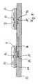
- an opto module 1is shown in plan view.
- an opto-semiconductor 3is an integrated one Circuit 4, which via a bond connection 5 is in electrical contact with the optical semiconductor 3, and further components, for example capacitors 6, 7 are arranged.
- the optical semiconductor 3 and the integrated circuit 4are each via bonds 8, 9 with wiring (not shown) connected on the carrier substrate 2, preferably formed in wiring levels (not shown) are.
- Such bond connectionscan of course also provided for the other components 6, 7 his.
- the wiring levelsallow for a complex and flexible design of the electrical Connections between the optical semiconductor 3, the integrated Circuit 4 and the other components 6, 7.
- Preferably one or more ground levelsare provided.
- the opto module 1As technologies for the production of the opto module 1, the "Chip Size Package” - or the “Ball Grid Array” technology be used. The application of these technologies in conjunction with the opto module 1 comprising the opto semiconductor 3 a high integration density of the individual components of the opto module 1.
- FIG. 2shows the opto module 1 from below.
- solder pads 11are arranged on the lower one Surface 10 of the opto module 1.
- the Solder pads 11form contact means for connecting the opto module 1 to external circuit components. With the help of the solder pads 11 For example, the opto module can be soldered onto a circuit board become.
- FIG. 3shows a cross-sectional illustration of the opto module 1.
- the solder pads 11have plated-through holes 12 connected, which are formed in the carrier substrate 2. On this way is between the solder pads 11 and the wiring plane (not shown) made an electrical contact, so that the optical semiconductor 3, the integrated Circuit 4 and the other components 6, 7 on the Solder pads 11, the via 12 and the wiring level can be connected to external circuit components can.
- the carrier substrate 2points in a region of the optical semiconductor 3 a through opening 13 (see FIG. 2).
- Through the Through opening 13passes light that from the Optical semiconductor 3 is emitted, and / or light that on the optical semiconductor 3 is to be coupled.
- Itcan be provided in the through opening 13 an optical Imaging element (not shown) to arrange the To redirect light and / or to focus on the optical semiconductor.
- Figure 4shows an enlarged view of a section of the opto module 1 according to FIGS. 1 to 3.
- a solder ball 14is arranged in each case.
- the use of the Solder balls 14enable a low inductance connection of the Optomodule 1 to external circuit components.
- the solder balls 14in particular have a lower inductance than connecting pins on how they are known from leadframe technology.
- the mass 16can be a casting compound or an injection compound and serves to protect the electrical components of the opto module 1.
- the mass 16can be made using known ones Manufacturing techniques are poured or sprayed on, how they integrated from the field of manufacturing Circuits are known. With the help of mass 16 is a mechanical Protection of the electrical components of the opto module 1 created.
- Cooling elementspreferably cooling plates, can be used for heat dissipation be encapsulated or encapsulated by the mass 16.
- the opto module 1 according to FIGS. 1 to 3can be produced be processed in such a way that it is on a PCB section 30 is soldered, as shown in Figure 5 is shown as an example. Between the circuit board section 30 and the opto module 1, a solder connection 29 is formed.
- the opto module 1is here on the circuit board section 30 positioned so that the through hole 13 in the carrier substrate 2 relative to one in the circuit board section 30 trained opening 31 is arranged, such that the light emitted by the optical semiconductor 3 through the through opening 13 in the carrier substrate 2 and the opening 31 in the circuit board section 30 can reach.
- a flange component 33On a surface 32 of the surface facing away from the opto module 1 Printed circuit board section 30 is a flange component 33 with Fixed with the aid of an adhesive connection 34.
- a plug pin 36In a recording section 35 of the flange component 33 is a plug pin 36 arranged.
- the plug pin 36comprises an optical waveguide 37, in which the emitted by the optical semiconductor 3 Light is injected.
- you can use the opto-semiconductor 3 lightcan also be coupled, which with the help of the optical fiber 37 is transmitted.
- the circuit board section 30is via a flexible conductor section 38 connected to a module circuit board 39.
- a module circuit board 39On the module circuit board 39 are a plurality of external components 40, 41, 42 mounted.
- an optical imaging element 44is arranged. It can this is an imaging lens (see FIG. 6).
- Figure 6shows a connection arrangement in which in a PCB section 50 formed an opening 51 in such a way is that in the opening 51, a flange member 52 partially can be inserted so that between an end Surface 53 of the flange member 52 and a lower surface 54 of the carrier substrate 2, an adhesive connection 55 is formed can be.
- the difference from the embodiment according to Figure 3is thus that a direct connection formed between the flange member 52 and the support substrate 2 is.
- Figure 6is between a transmitting / receiving surface 56 of the Optical semiconductor 3 and an end face 57 of an optical waveguide 58, an optical lens element 59 arranged to be optical To avoid losses.
- the optical lens elementis optimized here so that focus points 60, 61 on the transmission / reception surface 56 of the optical semiconductor 3 or generated on the end face 57 of the optical waveguide 58 become.
- FIG. 7shows an embodiment with an opto module 1 and a flange member 70, wherein, as in the embodiment in Figure 4, a direct attachment of the Flange component 70 on a lower surface 71 of the carrier substrate 2 is formed.
- the opto module 1is not using the solder pads 11 on a circuit board section is mounted, but the solder pads 11 with (leadframe) Connection pins 72 are connected.
- the leadframe materialcan also use the leadframe material to make a shield plate 73 can be formed, which in the same operation as the Connection pins 72 is soldered.
- the shield plate 73forms electromagnetic shielding for the opto module 1.
- Figure 8shows an application in which a first and a second opto module 80, 81, which the opto module 1 according to the figures 1a-1c are designed accordingly on a system circuit board 82 mounted with the help of solder connections 83 are.
- a System circuit board 82trained light channel 86 light signals be replaced. This is shown in FIG Arrows A, B indicated.
- the light signalsare here in Corner areas 87, 88 of the light channel 86 with the help of respective Deflecting mirror 89 or 90 deflected.
- FIGS. 9 to 11show an opto module 1 according to the figures 1 - 3 shown, in which the solder pads 11 with (leadframe) Connection pins 100 are connected.
- an optical component 102 for guiding the light emitted by the optical semiconductor 3arranged in the area of the through opening 13 of the carrier substrate 2 is on a lower surface 101 of the carrier substrate 2, an optical component 102 for guiding the light emitted by the optical semiconductor 3 arranged.
- the optical component 102is preferred here glued.
- the optical component 102can be used a deflection of the emitted light take place, one side surface 103 of the optical component 102 a Stop surface for a connector pin 104 with an optical fiber 105 forms.
- the emerging from the opto-semiconductor 3In this way, light can go directly into the optical fiber 105 of the connector pin 104 are coupled.
Landscapes
- Physics & Mathematics (AREA)
- General Physics & Mathematics (AREA)
- Optics & Photonics (AREA)
- Electromagnetism (AREA)
- Optical Couplings Of Light Guides (AREA)
- Light Receiving Elements (AREA)
Abstract
Translated fromGerman
Description
Translated fromGermanDie Erfindung liegt auf dem Gebiet optischer Bauelemente,insbesondere optischer Subkomponenten, die auch als Opto-ICsbezeichnet werden.The invention is in the field of optical components,especially optical subcomponents, also called opto-ICsbe designated.
Solche optischen Bauelemente werden benutzt, um optische Signalezu erzeugen, zu empfangen, umzuwandeln, zu verarbeitenusw. Es kann sich beispielsweise um eine PIN-Fotodiode-Vorverstärker-Kombinationhandeln. Es ist bekannt, die optischenSubkomponenten auf der Basis von TO46-Gehäusen zu bauen.Such optical components are used to generate optical signalsto generate, receive, transform, processetc. It can be, for example, a PIN-photodiode-preamplifier combinationact. It is known the opticalTo build subcomponents based on TO46 housings.
Aus dem Artikel von C. Schwantes: "Small Form Factor: HigherDensity For Fiber Based High Speed Networking", ElectronicComponents and Technology Conference IEEE, 1999, Seiten 539-542,sind optische Subkomponenten bzw. Optomodule auf der Basisder Leadframe-Technologie bekannt. Die zunehmendeVerbreitung und Anwendung von Optomodulen verlangt einen höherenGrad der Integrationsdichte, welcher mit diesen bekanntenTechniken nicht erreicht werden kann.From the article by C. Schwantes: "Small Form Factor: HigherDensity For Fiber Based High Speed Networking ", ElectronicComponents and Technology Conference IEEE, 1999, pages 539-542,are optical subcomponents or opto modules on the basisknown as leadframe technology. The increasingThe spread and application of opto modules requires a higher oneDegree of integration density, which with these knownTechniques cannot be achieved.
Aufgabe der vorliegenden Erfindung ist es deshalb, ein Optomodulzu schaffen, welches eine höhere Integrationsdichte derKomponenten des Optomoduls ermöglicht.The object of the present invention is therefore an opto moduleto create which has a higher integration density of theComponents of the opto module enables.
Diese Aufgabe wird erfindungsgemäß durch ein Optomodul gemäßAnspruch 1 gelöst. Das Optomodul umfaßt ein Trägersubstrat;Verdrahtungsmittel, die auf einer Vorderseite des Trägersubstratsaufgebracht sind; Kontaktmittel, die auf einer Rückseitedes Trägersubstrats angeordnet sind und über mindestenseine in dem Trägersubstrat ausgebildete Druchkontaktierungmit einer Leitung der Verdrahtungsmittel elektrisch verbundensind; und ein Optohalbleiter zum Senden und/oder Empfangenvon Licht, wobei der Optohalbleiter mit der Leitung der Verdrahtungsmittelin elektrischem Kontakt steht und auf einer Vorderseite des Trägersubstrats im Bereich einer in dem Trägersubstratausgebildeten Durchgangsöffnung so angeordnetist, daß das Licht durch die Durchgangsöffnung hindurch gesendetund/oder empfangen werden kann.This object is achieved according to the invention by an opto moduleClaim 1 solved. The opto module comprises a carrier substrate;Wiring means on a front side of the carrier substrateare upset; Contact agent on a backof the carrier substrate are arranged and over at leasta through-contact formed in the carrier substrateelectrically connected to a line of the wiring meansare; and an optical semiconductor for transmission and / or receptionof light, the opto-semiconductor with the line of the wiring meansis in electrical contact and on oneFront of the carrier substrate in the area of one in the carrier substratetrained through opening arrangedis that the light is sent through the through holeand / or can be received.
Der Erfindung liegt der wesentliche Gedanke zugrunde, beimAufbau und der Herstellung von Optomodulen mit einem OptohalbleiterTechnologien zu nutzen, wie sie beispielsweise fürintegrierte Schaltungen verwendet werden. Auf diese Weisewird eine hohe Integration der Komponenten des Optomodulsmöglich, da die Verdrahtung des Trägersubstrats wesentlichkomplexer und flexibler als bei den bekannten Techniken, beispielsweiseder Leadframe-Technologie realisiert werden kann.The invention is based on the essential idea whenConstruction and manufacture of opto modules with an opto semiconductorTo use technologies such as those used forintegrated circuits are used. In this wayhigh integration of the components of the opto modulepossible because the wiring of the carrier substrate is essentialmore complex and flexible than with the known techniques, for examplethe leadframe technology can be realized.
Ein wesentlicher Vorteil der Erfindung gegenüber dem Standder Technik besteht darin, daß eine verbesserte Hochfrequenztauglichkeitdes Optomoduls, insbesondere des Trägersubstratsgewährleistet ist. Dieses ist die Folge der verbesserten Verdrahtungsmöglichkeitenund kurzer Anbindungen von Hochfrequenzkomponenten,beispielsweise Kondensatoren in dem Trägersubstrat.A major advantage of the invention over the prior artThe technology is that improved radio frequency capabilitythe opto module, in particular the carrier substrateis guaranteed. This is the result of the improved wiring optionsand short connections of high-frequency components,for example capacitors in the carrier substrate.
Ein weiterer Vorteil der Erfindung besteht darin, daß Technologienund Verarbeitungsschritte genutzt werden können, fürderen Ausführung umfangreiche Erfahrungen im Zusammenhang mitder Herstellung integrierter Schaltungen bestehen.Another advantage of the invention is that technologiesand processing steps can be used fortheir execution extensive experience related tothe manufacture of integrated circuits.
Eine zweckmäßige Weiterbildung der Erfindung sieht vor, daßder Optohalbleiter auf einer vorderseitigen Oberfläche desTrägersubstrats angeordnet ist, wodurch ein einfaches und mitgeringem Aufwand ausführbares Aufbringen des Optohalbleitersermöglicht ist.An expedient development of the invention provides thatthe optical semiconductor on a front surface of theCarrier substrate is arranged, making a simple and withapplication of the optical semiconductor can be carried out with little effortis possible.
Bei einer vorteilhaften Ausgestaltung der Erfindung ist eineSchutzschicht vorgesehen, die den Optohalbleiter wenigstensteilweise umgibt und derart auf der Vorderseite des Trägersubstratsaufgebracht ist, daß eine im wesentlichen geschlossene Schutzoberfläche gebildet ist, wodurch bei der Verwendungbzw. dem Einsatz des Optomoduls ein Schutz vor mechanischenStöreinflüssen gebildet ist.In an advantageous embodiment of the inventionProtective layer provided that the opto semiconductor at leastpartially surrounds and so on the front of the carrier substrateis applied that a substantially closedProtective surface is formed, which in useor the use of the opto module, protection against mechanicalInterference is formed.
Zweckmäßig ist bei einer Ausführungsform auf der Vorderseitedes Trägersubstrats ein Bauelement angeordnet, das mit demOptohalbleiter und der Leitung der Verdrahtungsmittel inelektrischem Kontakt steht und zumindest teilweise von derSchutzschicht umgeben ist. Hierdurch ist eine Beschaltung desOptohalbleiters zum Betreiben und Steuern desselben ermöglicht.In one embodiment, it is useful on the frontof the carrier substrate, a component arranged with theOpto semiconductors and the wiring means inelectrical contact and at least partially from theProtective layer is surrounded. This is a circuit of theOpto semiconductor for operating and controlling the same.
Vorzugsweise ist die Schutzschicht von einer Vergußmasse odereiner Spritzmasse gebildet, wodurch die Schutzschicht mitHilfe bekannter Techniken auf einfache Art und Weise geschaffenwerden kann.The protective layer is preferably of a casting compound oran injection molding compound, whereby the protective layer withCreated with the help of known techniques in a simple mannercan be.
Eine hinsichtlich der Verwendung moderner Chip-Herstellungstechnologienbevorzugte Ausführungsform der Erfindung siehtvor, daß der Optohalbleiter und/oder das Bauelement jeweilsüber eine Bondverbindung mit der Leitung der Verdrahtungsmittelverbunden sind.One regarding the use of modern chip manufacturing technologiespreferred embodiment of the inventionbefore that the optical semiconductor and / or the component in each casevia a bond connection with the line of the wiring meansare connected.
Eine in Bezug auf die komplexe Verdrahtung und die verbesserteHochfrequenztauglichkeit bevorzugte Ausgestaltung derErfindung sieht vor, daß die Verdrahtungsmittel mindestenseine Verdrahtungsebene und eine Masseebene umfassen.One in terms of complex wiring and improvedHigh-frequency suitability preferred embodiment of theInvention provides that the wiring means at leastinclude a wiring level and a ground level.
Eine zweckmäßige Weiterbildung der Erfindung sieht vor, daßdas Trägersubstrat aus einem Leiterplattenmaterial gebildetist, wodurch für die Be- und Verarbeitung des Trägersubstratseine Vielzahl von bewährten Techniken zur Verfügung stehen.An expedient development of the invention provides thatthe carrier substrate is formed from a printed circuit board materialis, whereby for the processing and processing of the carrier substratea variety of proven techniques are available.
Eine hinsichtlich der störungsfreien Funktionalität des Optomodulszweckmäßige Ausgestaltung der Erfindung sieht vor, daßfür den Optohalbleiter und/oder das Bauelement eine Schirmungausgebildet ist, die mit Hilfe einer Schirmungsschicht gebildet ist, wobei sich die Schirmungsschicht im wesentlichenüber den gesamten Bereich des Trägersubstrats erstreckt.One regarding the trouble-free functionality of the opto moduleexpedient embodiment of the invention provides thatshielding for the optical semiconductor and / or the componentis formed, which is formed with the aid of a shielding layerwhere the shielding layer is essentiallyextends over the entire area of the carrier substrate.
Zur Erhöhung der Integrationsdichte des Optomoduls kann vorgesehensein, daß die Schirmungsschicht von dem Trägersubstratumfaßt ist.Provision can be made to increase the integration density of the optomodulebe that the shielding layer from the carrier substrateis included.
Eine induktivitätsarme Anbindung des Optomoduls kann beieiner zweckmäßigen Fortbildung der Erfindung dadurch gewährleistetwerden, daß die Kontaktmittel Lotbälle sind.A low inductance connection of the opto module can be used foran appropriate training of the invention thereby guaranteedbe that the contact means are solder balls.
Eine hinsichtlich der Flexibilität der Anbindung des Optomodulsbevorzugte Ausführungsform sieht vor, daß die Kontaktmitteljeweils mit Anschlußpins elektrisch verbunden sind.One in terms of the flexibility of connecting the opto modulepreferred embodiment provides that the contact meansare each electrically connected with connector pins.
Eine verbesserte Kopplung des von dem Optohalbleiter ausgesendetenLichts bzw. des auf den Optohalbleiter zu koppelndenLichts kann bei einer vorteilhaften Ausführungsform dadurcherreicht werden, daß in der Durchgangsöffnung ein optischesAbbildungselement angeordnet ist.An improved coupling of that emitted by the optical semiconductorLight or to be coupled to the optical semiconductorIn an advantageous embodiment, light can therebybe achieved that an optical in the through holeImaging element is arranged.
Eine hinsichtlich der Leitung des von dem Optohalbleiter ausgesendetenLichts zu einem anderen Bauelement, beispielsweiseeinem Stecker mit einem Lichtwellenleiter bevorzugte Ausgestaltungder Erfindung sieht vor, daß auf einer rückseitigenOberfläche des Trägersubstrats ein optisches Element angeordnetist, so daß das durch die Durchgangsöffnung hindurch tretendeLicht optisch geleitet werden kann.One with regard to the line of that emitted by the optical semiconductorLight to another component, for examplea connector with an optical fiber preferred embodimentthe invention provides that on a backAn optical element is arranged on the surface of the carrier substrateis so that that which passes through the through openingLight can be guided optically.
Die mit dem beschriebenen Optomodul verbundenen Vorteile erweiternund verbessern die Anwendungsmöglichkeiten des Optomodulsdann zweckmäßig, wenn eine Verbindungsanordnung miteinem solchen Optomodul und einem Leiterplattenabschnitt gebildetist, wobei die Kontaktmittel mit einer Verdrahtung desLeiterplattenabschnitts in elektrischem Kontakt stehen, unddas Optomodul mit Hilfe der Kontaktmittel auf dem Leiterplattenabschnittmontiert ist, so daß das Licht durch eine Öffnung in dem Leiterplattenabschnitt hindurch gesendet und/oderempfangen werden kann. Auf diese Weise ist eine flexible Anbindungdes Optomoduls an eine Vielzahl anderer Schaltungskomponentenbzw. Schaltungen möglich.Extend the advantages associated with the opto module describedand improve the possible uses of the opto modulethen useful when a connection arrangement withsuch an opto module and a circuit board sectionis, the contact means with a wiring of thePCB section are in electrical contact, andthe opto module using the contact means on the circuit board sectionis mounted so that the light through an openingsent through in the circuit board section and / orcan be received. This is a flexible connectionof the opto module to a variety of other circuit componentsor circuits possible.
Eine hohe Integration einer solchen Verbindungsanordnung kannbei einer bevorzugten Fortbildung der Erfindung dadurch erreichtwerden, daß in dem Leiterplattenabschnitt ein Lichtkanalausgebildet ist, so daß Sendelicht, welches von dem Optohalbleiterdurch die Durchgangsöffnung in dem Trägersubstrathindurch gesendet wird, in den Lichtkanal eingekoppelt werdenkann, und Empfangslicht aus dem Lichtkanal durch die Durchgangsöffnungin dem Trägersubstrat hindurch auf den Optohalbleitergekoppelt werden kann.A high level of integration of such a connection arrangement canachieved in a preferred development of the inventionthat a light channel in the circuit board sectionis formed so that transmission light emitted by the optical semiconductorthrough the through opening in the carrier substrateis sent through, can be coupled into the light channelcan, and receiving light from the light channel through the through holein the carrier substrate onto the optical semiconductorcan be coupled.
Eine Führung des Lichts in dem Lichtkanal ist bei einer vorteilhaftenAusführungsform mit Hilfe eines in dem Lichtkanalangeordneten optischen Umlenkmittels und/oder eines optischenAbbildungsmittels ermöglicht.Guiding the light in the light channel is advantageousEmbodiment using one in the light channelarranged optical deflection means and / or an opticalImaging means enabled.
Bei einer bevorzugten Weiterbildung der Erfindung kann vorgesehensein, daß in der Öffnung des Leiterplattenabschnittsein Abschnitt eines Flanschbauteils angeordnet ist, so daßzwischen einem stirnseitigen Oberflächenabschnitt desFlanschbauteils und einem rückseitigen Oberflächenabschnittdes Trägersubstrats eine Verbindung ausgebildet ist, wobeidas Flanschbauteil einen Aufnahmeabschnitt zur wenigstensteilweisen Aufnahme eines Steckerbauteils aufweist, und wobeidas Steckerbauteil in dem Aufnahmeabschnitt so angeordnetist, daß das vom Optohalbleiter ausgesendete und/oder das vomOptohalbleiter empfangene Licht in das Steckerbauteil eingekoppeltbzw. aus dem Steckerbauteil ausgekoppelt werden kann.Hierdurch ist eine kompakte Kopplung zwischen dem Optomodulund einem zur Anbindung verschiedener Bauteile nutzbarenFlanschbauteil ermöglicht.In a preferred development of the invention can be providedbe that in the opening of the circuit board sectiona portion of a flange member is arranged so thatbetween an end surface section of theFlange component and a rear surface portiona connection of the carrier substrate is formed, whereinthe flange component has a receiving section for at leasthas a partial receptacle of a plug component, and whereinthe connector component is arranged in the receiving sectionis that the emitted by the optical semiconductor and / or that ofOptical semiconductor received light coupled into the connector componentor can be coupled out of the plug component.This is a compact coupling between the opto moduleand one that can be used to connect various componentsFlange component allows.
Eine hinsichtlich der mechanischen Belastbarkeit der Verbindungsanordnungbevorzugte Weiterbildung der Erfindung siehtvor, daß auf einer von dem Optomodul abgewandten Oberflächedes Leiterplattenabschnitts im Bereich der Öffnung des Leiterplattenabschnittsein Flanschbauteil angeordnet ist, wobeidas Flanschbauteil einen Aufnahmeabschnitt zur wenigstensteilweisen Aufnahme eines Steckerbauteils aufweist, und wobeidas Steckerbauteil in dem Aufnahmeabschnitt so angeordnetist, daß das vom Optohalbleiter ausgesendete und/oder das vomOptohalbleiter empfangene Licht in das Steckerbauteil gekoppeltbzw. aus dem Steckerbauteil ausgekoppelt werden kann.One with regard to the mechanical strength of the connection arrangementpreferred development of the invention seesbefore that on a surface facing away from the opto moduleof the circuit board section in the area of the opening of the circuit board sectiona flange component is arranged, whereinthe flange component has a receiving section for at leasthas a partial receptacle of a plug component, and whereinthe connector component is arranged in the receiving sectionis that the emitted by the optical semiconductor and / or that ofOpto semiconductor received light coupled into the connector componentor can be coupled out of the plug component.
Zur Vermeidung optischer Verluste kann bei einer zweckmäßigenFortbildung der Erfindung vorgesehen sein, daß in demFlanschbauteil ein optisches Abbildungselement zum Einkoppelnund/oder zum Auskoppeln des Licht in das bzw. aus dem Steckerbauteilangeordnet ist.In order to avoid optical losses, an appropriateTraining of the invention should be provided that in theFlange component an optical imaging element for couplingand / or for coupling the light into or out of the plug componentis arranged.
Die Erfindung wird im Folgenden anhand von Ausführungsbeispielenunter Bezugnahme auf eine Zeichnung näher erläutert.Hierbei zeigen:
- Figuren 1 bis 3
- ein Optomodul von oben, von unten bzw. ineiner Querschnittsdarstellung;
Figur 4- einen vergrößerten Teilabschnitt des Optomodulsnach
Figur 3; Figur 5- eine Verbindungsanordnung mit einem Optomodulnach
Figur 3 und einem
Leiterplattenabschnitt, wobei dieVerbindungsanordnung an ein Flanschbauteilgekoppelt ist; Figur 6- eine vergrößerte Darstellung der Verbindungsanordnungnach
Figur 5; - Figur 7
- die Anordnung eines Optomoduls nach
Figur 3auf einem Flanschbauteil, wobei das Optomodulteilweise von einer Schirmung umfaßt ist; Figur 8- eine Anordnung mit einem Leiterplattenabschnittund zwei hierauf angeordneten Optomodulennach
Figur 3; und - Figuren 9 - 11
- eine Ausführungsform eines Optomoduls mitAnschlußpins in Draufsicht, in Vorderansichtund in Seitenansicht.
- Figures 1 to 3
- an opto module from above, from below or in a cross-sectional view;
- Figure 4
- an enlarged portion of the opto module of Figure 3;
- Figure 5
- a connection arrangement with an opto module according to Figure 3 and
Printed circuit board section, wherein the connection arrangement is coupled to a flange component; - Figure 6
- an enlarged view of the connection arrangement of Figure 5;
- Figure 7
- the arrangement of an opto module according to Figure 3 on a flange component, the opto module is partially covered by a shield;
- Figure 8
- an arrangement with a circuit board section and two optomodules arranged thereon according to Figure 3; and
- Figures 9-11
- an embodiment of an opto module with connection pins in plan view, in front view and in side view.
In Figur 1 ist ein Optomodul 1 in Draufsicht dargestellt. Aufeinem Trägersubstrat 2 sind ein Optohalbleiter 3 ein integrierterSchaltkreis 4, welcher über eine Bondverbindung 5mit dem Optohalbleiter 3 in elektrischem Kontakt steht, sowieweitere Bauteile, beispielsweise Kondensatoren 6, 7 angeordnet.Der Optohalbleiter 3 und der integrierte Schaltkreis 4sind jeweils über Bondverbindungen 8, 9 mit Verdrahtungen(nicht dargestellt) verbunden, die auf dem Trägersubstrat 2,vorzugsweise in Verdrahtungsebenen (nicht dargestellt) ausgebildetsind. Derartige Bondverbindungen können selbstverständlichauch für die weiteren Bauelemente 6, 7 vorgesehensein. Die Verdrahtungsebenen ermöglichen hierbei eine komplexeund flexibel gestaltbare Ausführung der elektrischenVerbindungen zwischen dem Optohalbleiter 3, dem integriertenSchaltkreis 4 und den weiteren Bauelementen 6, 7. Auf dieseWeise können Optomodule mit komplizierten Verdrahtungswegenund Schaltungsanordnungen hergestellt werden. Vorzugsweisesind ein oder mehrere Masseebenen vorgesehen.In Figure 1, an opto module 1 is shown in plan view. Ona
Als Technologien zur Herstellung des Optomoduls 1 können die"Chip Size Package"- oder die "Ball Grid Array"-Technologiegenutzt werden. Die Anwendung dieser Technologien in Verbindungmit dem den Optohalbleiter 3 umfassenden Optomodul 1 ermöglicht eine hohe Integrationsdichte der einzelnen Komponentendes Optomoduls 1.As technologies for the production of the opto module 1, the"Chip Size Package" - or the "Ball Grid Array" technologybe used. The application of these technologies in conjunctionwith the opto module 1 comprising the opto semiconductor 3a high integration density of the individual componentsof the opto module 1.
Figur 2 zeigt das Optomodul 1 von unten. Auf der unterenOberfläche 10 des Optomodul 1 sind Lötpads 11 angeordnet. DieLötpads 11 bilden Kontaktmittel zum Anbinden des Optomoduls 1an äußere Schaltungskomponenten. Mit Hilfe der Lötpads 11kann das Optomodul beispielsweise auf eine Leiterplatte aufgelötetwerden.Figure 2 shows the opto module 1 from below. On the lower one
Figur 3 zeigt eine Querschnittsdarstellung des Optomoduls 1.Gemäß Figur 3 sind die Lötpads 11 mit Durchkontaktierungen 12verbunden, die in dem Trägersubstrat 2 ausgebildet sind. Aufdiese Weise wird zwischen den Lötpads 11 und der Verdrahtungsebene(nicht dargestellt) ein elektrischer Kontakt hergestellt,so daß der Optohalbleiter 3, der integrierteSchaltkreis 4 sowie die weiteren Bauelemente 6, 7 über dieLötpads 11, die Durchkontaktierung 12 und die Verdrahtungsebenemit externen Schaltungskomponenten verbunden werdenkönnen.FIG. 3 shows a cross-sectional illustration of the opto module 1.According to FIG. 3, the solder pads 11 have plated-through
Das Trägersubstrat 2 weist in einem Bereich des Optohalbleiters3 eine Durchgangsöffnung 13 auf (vgl. Fig. 2). Durch dieDurchgangsöffnung 13 hindurch gelangt Licht, das von demOptohalbleiter 3 ausgesendet wird, und/oder Licht, das aufden Optohalbleiter 3 gekoppelt werden soll. Es kannvorgesehen sein, in der Durchgangsöffnung 13 ein optischesAbbildungselement (nicht dargestellt) anzuordnen, um dasLicht umzulenken und/oder auf den Optohalbleiter zu fokussieren.The
Figur 4 zeigt eine vergrößerte Darstellung eines Abschnittsdes Optomoduls 1 nach den Figuren 1 bis 3. Auf den Lötpads 11ist jeweils ein Lotball 14 angeordnet. Die Verwendung derLotbälle 14 ermöglicht eine induktivitätsarme Anbindung desOptomoduls 1 an äußere Schaltungskomponenten. Die Lotbälle 14 weisen insbesondere eine geringere Induktivität als Anschlußpinsauf, wie sie aus der Leadframe-Technologie bekannt sind.Figure 4 shows an enlarged view of a sectionof the opto module 1 according to FIGS. 1 to 3. On the solder pads 11a
Gemäß den Figuren 3 und 4 ist auf einer oberen Oberfläche 15des Trägersubstrats 2 eine Masse 16 aufgebracht, die den Optohalbleiter3, den integrierten Schaltkreis 4, die weiterenBauelemente 6, 7 sowie die Bondverbindungen 5, 8 bzw. 9 einhüllt.Die Masse 16 kann eine Vergußmasse oder eine Spritzmassesein und dient dem Schutz der elektrischen Komponentendes Optomoduls 1. Die Masse 16 kann unter Verwendung bekannterHerstellungstechniken aufgegossen bzw. aufgespritzt werden,wie sie aus dem Bereich der Herstellung integrierterSchaltkreise bekannt sind. Mit Hilfe der Masse 16 ist ein mechanischerSchutz der elektrischen Komponenten des Optomoduls1 geschaffen.According to FIGS. 3 and 4, 15 is on an upper surfaceof the
Zur Wärmeableitung können Kühlkörper, vorzugsweise Kühlblechevon der Masse 16 umgossen oder umspritzt sein.Cooling elements, preferably cooling plates, can be used for heat dissipationbe encapsulated or encapsulated by the
Das Optomodul 1 gemäß den Figuren 1 bis 3 kann nach der Herstellungderart weiterverarbeitet werden, daß es auf einemLeiterplattenabschnitt 30 aufgelötet wird, wie dies in Figur5 beispielhaft dargestellt ist. Zwischen dem Leiterplattenabschnitt30 und dem Optomodul 1 ist eine Lötverbindung 29 ausgebildet.Das Optomodul 1 ist hierbei auf dem Leiterplattenabschnitt30 positioniert, so daß die Durchgangsöffnung 13 indem Trägersubstrat 2 relativ zu einer in dem Leiterplattenabschnitt30 ausgebildeten Öffnung 31 angeordnet ist, derart,daß das Licht, welches von dem Optohalbleiter 3 ausgesendetwird, durch die Durchgangsöffnung 13 in dem Trägersubstrat 2und die Öffnung 31 in dem Leiterplattenabschnitt 30 hindurchgelangen kann.The opto module 1 according to FIGS. 1 to 3 can be producedbe processed in such a way that it is on a
Auf einer von dem Optomodul 1 abgewandten Oberfläche 32 desLeiterplattenabschnitts 30 ist ein Flanschbauteil 33 mitHilfe einer Klebeverbindung 34 befestigt. In einem Aufnahmeabschnitt 35 des Flanschbauteils 33 ist ein Steckerstift 36angeordnet. Der Steckerstift 36 umfaßt einen Lichtwellenleiter37, in den das von dem Optohalbleiter 3 ausgesendeteLicht eingekoppelt wird. Selbstverständlich kann auf den Optohalbleiter3 auch Licht gekoppelt werden, welches mit Hilfedes Lichtwellenleiters 37 übertragen wird.On a
Der Leiterplattenabschnitt 30 ist über einen Flexleiterabschnitt38 mit einer Modulleiterplatte 39 verbunden. Aufder Modulleiterplatte 39 sind mehrere externe Bauelemente 40,41, 42 montiert. Der Optohalbleiter 3, welcher über die Lötverbindung29 mit der Verdrahtung des Leiterplattenabschnitts30 in Verbindung steht, kann auf diese Weise unter Einbeziehungdes Flexleiterabschnitts 38 und der Modulleiterplatte 39an die externen Bauelemente 40, 41 bzw. 42 gekoppelt werden.An der Modulleiterplatte 39 ist weiterhin ein Anschlußstift43 ausgebildet, welcher es ermöglicht, die Modulleiterplatte39 auf einen Sockel zu stecken.The
Zur Vermeidung von optischen Verlusten beim Einkoppeln desLichts in den Lichtwellenleiter 37 bzw. beim Koppeln vonLicht auf den Optohalbleiter 3 ist in dem Flanschbauteil 36ein optisches Abbildungselement 44 angeordnet. Es kann sichhierbei um eine Abbildungslinse handeln (vgl. Figur 6).To avoid optical losses when coupling theLight in the
Figur 6 zeigt eine Verbindungsanordnung, bei der in einemLeiterplattenabschnitt 50 eine Öffnung 51 derart ausgebildetist, daß in die Öffnung 51 ein Flanschbauteil 52 teilweiseeingeführt werden kann, so daß zwischen einer stirnseitigenOberfläche 53 des Flanschbauteils 52 und einer unteren Oberfläche54 des Trägersubstrats 2 eine Klebeverbindung 55 ausgebildetwerden kann. Der Unterschied zu der Ausführungsformnach Figur 3 besteht somit darin, daß eine direkte Verbindungzwischen dem Flanschbauteil 52 und dem Trägersubstrat 2 gebildetist.Figure 6 shows a connection arrangement in which in a
In Figur 6 ist zwischen einer Sende-/Empfangsfläche 56 desOptohalbleiters 3 und einer Stirnfläche 57 eines Lichtwellenleiters58 ein optisches Linsenelement 59 angeordnet, um optischeVerluste zu vermeiden. Das optische Linsenelement isthierbei dahingehend optimiert, daß Fokussierungspunkte 60, 61auf der Sende-/Empfangsoberfläche 56 des Optohalbleiters 3bzw. auf der Stirnfläche 57 des Lichtwellenleiters 58 erzeugtwerden.In Figure 6 is between a transmitting / receiving
In Figur 7 ist eine Ausführungsform mit einem Optomodul 1 undeinem Flanschbauteil 70 dargestellt, wobei, wie bei der Ausführungsformin Figur 4, eine direkte Befestigung desFlanschbauteils 70 auf einer unteren Oberfläche 71 des Trägersubstrats2 gebildet ist. Ein Unterschied zur Ausführungsformnach Figur 4 besteht darin, daß das Optomodul 1 nichtmit Hilfe der Lötpads 11 auf einem Leiterplattenabschnittmontiert ist, sondern die Lötpads 11 mit (Leadframe-)Anschlußpins 72 verbunden sind. Bei dieser Ausführungsformkann mit Hilfe des Leadframe-Materials auch ein Schirmblech73 ausgeformt werden, welches im gleichen Arbeitsgang wie dieAnschlußpins 72 aufgelötet wird. Das Schirmblech 73 bildeteine elektromagnetische Schirmung für das Optomodul 1.FIG. 7 shows an embodiment with an opto module 1 anda
Figur 8 zeigt eine Anwendung, bei der ein erstes und einzweites Optomodul 80, 81, welche dem Optomodul 1 nach den Figuren1a-1c entsprechend ausgebildet sind, auf einer Systemleiterplatte82 mit Hilfe von Lötverbindungen 83 montiertsind. Zwischen jeweiligen Optohalbleitern 84, 85 des erstenund des zweiten Optomoduls 80, 81 können über einen in derSystemleiterplatte 82 ausgebildeten Lichtkanal 86 Lichtsignaleausgetauscht werden. Dieses ist in Figur 6 mit Hilfe vonPfeilen A, B angedeutet. Die Lichtsignale werden hierbei inEckbereichen 87, 88 des Lichtkanals 86 mit Hilfe jeweiligerUmlenkspiegel 89 bzw. 90 umgelenkt.Figure 8 shows an application in which a first and a
In den Figuren 9 bis 11 ist ein Optomodul 1 nach den Figuren1 - 3 dargestellt, bei dem die Lötpads 11 mit (Leadframe-)Anschlußpins 100 verbunden sind. Im Bereich der Durchgangsöffnung13 des Trägersubstrats 2 ist auf einer unteren Oberfläche101 des Trägersubstrats 2 ein optisches Bauelement 102zum Leiten des von dem Optohalbleiter 3 ausgesandten Lichtsangeordnet. Das optische Bauelement 102 ist hierbei vorzugsweiseaufgeklebt.FIGS. 9 to 11 show an opto module 1 according to the figures1 - 3 shown, in which the solder pads 11 with (leadframe)Connection pins 100 are connected. In the area of the through opening13 of the
Gemäß Figur 11 kann mit Hilfe des optischen Bauelements 102eine Umlenkung des ausgesendeten Lichts erfolgen, wobei eineseitliche Oberfläche 103 des optischen Bauelements 102 eineAnschlagfläche für einen Steckerstift 104 mit einem Lichtwellenleiter105 bildet. Das aus dem Optohalbleiter 3 austretendeLicht kann auf diese Weise direkt in den Lichtwellenleiter105 des Steckerstifts 104 eingekoppelt werden. Selbstverständlichist in gleicher Weise das Koppeln von Licht ausdem Lichtwellenleiter 105 auf den Optohalbleiter 3 möglich.According to FIG. 11, the
Claims (21)
Translated fromGermandadurch gekennzeichnet, daß derOptohalbleiter (3) auf einer vorderseitigen Oberfläche(15) des Trägersubstrats (2) angeordnet ist.Optomodule (1) according to claim 1,
characterized in that the optical semiconductor (3) is arranged on a front surface (15) of the carrier substrate (2).
gekennzeichnet durch
eine Schutzschicht, die den Optohalbleiter (3) wenigstensteilweise umgibt und derart auf der Vorderseite desTrägersubstrats (2) aufgebracht ist, daß eine imwesentlichen geschlossene Schutzoberfläche gebildet ist.Optomodule (1) according to claim 1 or 2,
marked by
a protective layer which at least partially surrounds the optical semiconductor (3) and is applied to the front of the carrier substrate (2) such that an essentially closed protective surface is formed.
dadurch gekennzeichnet, daß auf der Vorderseite des Trägersubstrats (2) einBauelement (4, 6 bzw. 7) angeordnet ist, das mit demOptohalbleiter (3) und der Leitung der Verdrahtungsmittelin elektrischem Kontakt steht und zumindest teilweise vonder Schutzschicht (16) umgeben ist.Optomodule (1) according to claim 3,
characterized in that a component (4, 6 or 7) is arranged on the front of the carrier substrate (2), which is in electrical contact with the optical semiconductor (3) and the line of the wiring means and at least partially from the protective layer (16) is surrounded.
dadurch gekennzeichnet,daß die Schutzschicht (16) von einer Vergußmasse gebildetist.Optomodule (1) according to claim 3 or 4,
characterized in that the protective layer (16) is formed by a potting compound.
dadurch gekennzeichnet,daß die Schutzschicht (16) von einer Spritzmasse gebildetist.Optomodule (1) according to claim 3 or 4,
characterized in that the protective layer (16) is formed by an injection molding compound.
dadurch gekennzeichnet,daß der Optohalbleiter (3) und/oder das Bauelement (4, 6bzw. 7) jeweils über mindestens eine Bondverbindung ( 8bzw. 9) mit der Leitung der Verdrahtungsmittel verbundensind.Optomodule (1) according to one of the preceding claims,
characterized in that the optical semiconductor (3) and / or the component (4, 6 or 7) are each connected to the line of the wiring means via at least one bond connection (8 or 9).
dadurch gekennzeichnet,daß die Verdrahtungsmittel mindestens eineVerdrahtungsebene und eine Masseebene umfassen.Optomodule (1) according to one of the preceding claims,
characterized in that the wiring means comprise at least one wiring level and one ground level.
dadurch gekennzeichnet,daß das Trägersubstrat (2) aus einemLeiterplattenmaterial gebildet ist.Optomodule (1) according to one of the preceding claims,
characterized in that the carrier substrate (2) is formed from a printed circuit board material.
gekennzeichnet durch eine
elektromagnetische Schirmung für den Optohalbleiter (3)und/oder das Bauelement (4, 6 bzw. 7), die mit Hilfeeiner Schirmungsschicht gebildet ist, wobei sich dieSchirmungsschicht im wesentlichen über den gesamtenBereich des Trägersubstrats (2) erstreckt.Optomodule (1) according to one of the preceding claims,
characterized by a
electromagnetic shielding for the optical semiconductor (3) and / or the component (4, 6 or 7), which is formed with the aid of a shielding layer, the shielding layer extending essentially over the entire area of the carrier substrate (2).
dadurch gekennzeichnet,daß die Schirmungsschicht von dem Trägersubstrat (2)umfaßt ist.Optomodule (1) according to claim 10,
characterized in that the shielding layer is surrounded by the carrier substrate (2).
dadurch gekennzeichnet,daß die Kontaktmittel Lotbälle (14) sind.Optomodule (1) according to one of the preceding claims,
characterized in that the contact means are solder balls (14).
dadurch gekennzeichnet,daß die Kontaktmittel jeweils mit Anschlußpins (100)mechanisch und elektrisch verbunden sind.Optomodule (1) according to one of the preceding claims,
characterized in that the contact means are each mechanically and electrically connected to connection pins (100).
dadurch gekennzeichnet,daß in der Durchgangsöffnung (13) ein optischesAbbildungselement angeordnet ist.Optomodule (1) according to one of the preceding claims,
characterized in that an optical imaging element is arranged in the through opening (13).
dadurch gekennzeichnet,daß auf einer rückseitigen Oberfläche des Trägersubstrats(3) ein optisches Element (102) angeordnet ist, so daßdas durch die Durchgangsöffnung (13) hindurch tretendeLicht optisch geleitet werden kann.Optomodule (1) according to one of the preceding claims,
characterized in that an optical element (102) is arranged on a rear surface of the carrier substrate (3) so that the light passing through the through opening (13) can be optically guided.
dadurch gekennzeichnet, daß die Kontaktmittel mit einer Verdrahtung desLeiterplattenabschnitts in elektrischem Kontakt stehen,und daß das Optomodul (1) mit Hilfe der Kontaktmittel aufdem Leiterplattenabschnitt (30; 50; 82) montiert ist, sodaß das Licht durch eine Öffnung (31 bzw. 51) in demLeiterplattenabschnitt (30; 50; 82) hindurch gesendetund/oder empfangen werden kann.Connection arrangement with an opto module (1) according to one of Claims 1 to 14 and a circuit board section,
characterized in that the contact means are in electrical contact with a wiring of the circuit board section, and that the optomodule (1) is mounted on the circuit board section (30; 50; 82) with the aid of the contact means, so that the light passes through an opening (31 or 51) can be transmitted and / or received in the circuit board section (30; 50; 82).
dadurch gekennzeichnet,daß in dem Leiterplattenabschnitt (82) ein Lichtkanal(86) ausgebildet ist, so daß Sendelicht, welches von demOptohalbleiter (3) durch die Durchgangsöffnung (13) indem Trägersubstrat (2) hindurch gesendet wird, in denLichtkanal (86) eingekoppelt werden kann, undEmpfangslicht aus dem Lichtkanal (86) durch dieDurchgangsöffnung (13) in dem Trägersubstrat (2) hindurchauf den Optohalbleiter (3) gekoppelt werden kann.Connection arrangement according to claim 16,
characterized in that a light channel (86) is formed in the circuit board section (82) so that transmission light which is transmitted from the optical semiconductor (3) through the through opening (13) in the carrier substrate (2) into the light channel (86 ) can be coupled in, and receiving light from the light channel (86) can be coupled through the through opening (13) in the carrier substrate (2) onto the optical semiconductor (3).
dadurch gekennzeichnet,daß in dem Lichtkanal ein optisches Umlenkmittel (89; 90)und/oder eine optisches Abbildungsmittel angeordnet sind.Connection arrangement according to claim 17,
characterized in that an optical deflection means (89; 90) and / or an optical imaging means are arranged in the light channel.
dadurch gekennzeichnet,daß in der Öffnung (51) des Leiterplattenabschnitts (50)ein Abschnitt eines Flanschbauteils (52) angeordnet ist,so daß zwischen einem stirnseitigen Oberflächenabschnitt(53) des Flanschbauteils (52) und einem rückseitigenOberflächenabschnitt (54) des Trägersubstrats (2) eineVerbindung (55) ausgebildet ist, wobei das Flanschbauteil(52) einen Aufnahmeabschnitt zur wenigstens teilweisenAufnahme eines Steckerbauteils (58) aufweist, und wobeidas Steckerbauteil (58) in dem Aufnahmeabschnitt so angeordnet ist, daß das vom Optohalbleiter (3)ausgesendete und/oder das vom Optohalbleiter (3)empfangene Licht in das Steckerbauteil (58) eingekoppeltbzw. aus dem Steckerbauteil (58) ausgekoppelt werdenkann.Connection arrangement according to claim 16,
characterized in that a section of a flange component (52) is arranged in the opening (51) of the printed circuit board section (50), so that between an end surface section (53) of the flange component (52) and a rear surface section (54) of the carrier substrate (2 ) a connection (55) is formed, the flange component (52) having a receiving section for at least partially receiving a connector component (58), and wherein the connector component (58) is arranged in the receiving section such that it is emitted by the optical semiconductor (3) and / or the light received by the optical semiconductor (3) can be coupled into the plug component (58) or can be coupled out of the plug component (58).
dadurch gekennzeichnet,daß auf einer von dem Optomodul (1) abgewandtenOberfläche (32) des Leiterplattenabschnitts (30), imBereich der Öffnung (31) des Leiterplattenabschnitts (30)ein Flanschbauteil (33) angeordnet ist, wobei dasFlanschbauteil (33) einen Aufnahmeabschnitt (35) zurwenigstens teilweisen Aufnahme eines Steckerbauteils (36)aufweist, und wobei das Steckerbauteil (36) in demAufnahmeabschnitt (35) so angeordnet ist, daß das vomOptohalbleiter (3) ausgesendete und/oder das vomOptohalbleiter (3) empfangene Licht in das Steckerbauteil(36) eingekoppelt bzw. aus dem Steckerbauteil (36)ausgekoppelt werden kann.Connection arrangement according to claim 16,
characterized in that a flange component (33) is arranged on a surface (32) of the circuit board section (30) facing away from the opto module (1), in the region of the opening (31) of the circuit board section (30), the flange component (33) having a Receiving section (35) for at least partially receiving a connector component (36), and wherein the connector component (36) is arranged in the receiving section (35) so that that emitted by the optical semiconductor (3) and / or received by the optical semiconductor (3) Light can be coupled into the plug component (36) or can be coupled out of the plug component (36).
dadurch gekennzeichnet,daß in dem Flanschbauteil (33; 52) ein optischesAbbildungselement (44; 59) zum Einkoppeln und/oder zumAuskoppeln des Lichts in das bzw. aus dem Steckerbauteil(33; 52) angeordnet ist.Connection arrangement according to claim 19 or 20,
characterized in that an optical imaging element (44; 59) is arranged in the flange component (33; 52) for coupling and / or for coupling the light into and out of the plug component (33; 52).
Applications Claiming Priority (2)
| Application Number | Priority Date | Filing Date | Title |
|---|---|---|---|
| DE10032796 | 2000-06-28 | ||
| DE10032796ADE10032796A1 (en) | 2000-06-28 | 2000-06-28 | optomodule |
Publications (2)
| Publication Number | Publication Date |
|---|---|
| EP1168022A2true EP1168022A2 (en) | 2002-01-02 |
| EP1168022A3 EP1168022A3 (en) | 2004-09-08 |
Family
ID=7647957
Family Applications (1)
| Application Number | Title | Priority Date | Filing Date |
|---|---|---|---|
| EP01250221AWithdrawnEP1168022A3 (en) | 2000-06-28 | 2001-06-15 | Opto-module with substrate having through-hole connections |
Country Status (3)
| Country | Link |
|---|---|
| US (1) | US6483960B2 (en) |
| EP (1) | EP1168022A3 (en) |
| DE (1) | DE10032796A1 (en) |
Cited By (3)
| Publication number | Priority date | Publication date | Assignee | Title |
|---|---|---|---|---|
| EP1447696A1 (en)* | 2003-02-04 | 2004-08-18 | Infineon Technologies AG | Modular system of optoelectronic components and optoelectronic components to be used in the system |
| EP1480063A3 (en)* | 2003-05-19 | 2005-09-07 | Infineon Technologies AG | Opto-electronic modules for transmission and/or reception |
| EP2650852A1 (en)* | 2012-12-10 | 2013-10-16 | Siemens Aktiengesellschaft | Optical receiving unit, in particular for an optical smoke alarm that operates based on the scattered light principle |
Families Citing this family (14)
| Publication number | Priority date | Publication date | Assignee | Title |
|---|---|---|---|---|
| DE10214121C1 (en)* | 2002-03-28 | 2003-12-24 | Osram Opto Semiconductors Gmbh | Optoelectronic component with several semiconductor chips |
| JP4085697B2 (en)* | 2002-05-29 | 2008-05-14 | 住友電気工業株式会社 | Optical link module |
| US6823127B2 (en)* | 2002-09-05 | 2004-11-23 | Intel Corporation | Apparatus for holding a fiber array |
| US7263248B2 (en)* | 2003-02-11 | 2007-08-28 | Avago Technologies Fiber Ip (Singapore) Pte. Ltd. | Optical via to pass signals through a printed circuit board |
| JP2004246279A (en)* | 2003-02-17 | 2004-09-02 | Seiko Epson Corp | Optical module and manufacturing method thereof, optical communication device, opto-electric hybrid integrated circuit, circuit board, electronic equipment |
| JP2004354532A (en)* | 2003-05-27 | 2004-12-16 | Seiko Epson Corp | Optical module and manufacturing method thereof, optical communication device, electronic equipment |
| DE10332015A1 (en)* | 2003-07-14 | 2005-03-03 | Infineon Technologies Ag | Optoelectronic module with transmitter chip and connector for the module to an optical fiber and to a circuit board, and method of making the same |
| US7263256B2 (en)* | 2004-04-02 | 2007-08-28 | Samsung Electronics Co., Ltd. | Optical connection block, optical module, and optical axis alignment method using the same |
| DE102004016949A1 (en) | 2004-04-06 | 2005-12-22 | Siemens Ag | Detector module for an X-ray CT scanner |
| DE102006012780B3 (en)* | 2006-03-17 | 2007-06-06 | Infineon Technologies Ag | Optical coupler for interconversion of optical and electrical signals for mobile phones and cameras has optical and integrated circuit semiconductor chips in housing with light conductor and conductive film contact |
| DE102006061722B4 (en)* | 2006-12-28 | 2010-04-01 | Infineon Technologies Ag | Connection module and method for producing the same |
| DE102012217197B4 (en)* | 2012-09-24 | 2025-08-21 | Ifm Electronic Gmbh | Optical proximity switch |
| TWI617852B (en)* | 2014-10-16 | 2018-03-11 | 英屬開曼群島商鴻騰精密科技股份有限公司 | Optical module |
| CN112652611A (en)* | 2020-12-18 | 2021-04-13 | 维沃移动通信有限公司 | Sensor packaging structure and electronic equipment |
Family Cites Families (10)
| Publication number | Priority date | Publication date | Assignee | Title |
|---|---|---|---|---|
| US4268113A (en)* | 1979-04-16 | 1981-05-19 | International Business Machines Corporation | Signal coupling element for substrate-mounted optical transducers |
| DE3429282A1 (en)* | 1984-08-08 | 1985-04-11 | Siemens AG, 1000 Berlin und 8000 München | Optoelectronic module |
| DE3566169D1 (en)* | 1984-09-24 | 1988-12-15 | Siemens Ag | Opto-electronic device |
| DE19616969A1 (en)* | 1996-04-27 | 1997-10-30 | Bosch Gmbh Robert | Optical assembly for coupling an optical waveguide and method for producing the same |
| DE19635583A1 (en)* | 1996-09-02 | 1998-03-05 | Siemens Ag | Optoelectronic transmitter and / or receiver module |
| US5973337A (en)* | 1997-08-25 | 1999-10-26 | Motorola, Inc. | Ball grid device with optically transmissive coating |
| DE19826648B4 (en)* | 1998-06-16 | 2005-07-28 | Siemens Ag | Circuit carrier with an optical layer and optoelectronic component |
| DE19834090A1 (en)* | 1998-07-29 | 2000-02-03 | Heidenhain Gmbh Dr Johannes | Optoelectronic transmitter and receiver unit |
| JP2000081524A (en)* | 1998-09-07 | 2000-03-21 | Sony Corp | Light transmitter-receiver system |
| JP2001059923A (en)* | 1999-06-16 | 2001-03-06 | Seiko Epson Corp | Optical module and manufacturing method thereof, semiconductor device, and optical transmission device |
- 2000
- 2000-06-28DEDE10032796Apatent/DE10032796A1/ennot_activeCeased
- 2001
- 2001-06-15EPEP01250221Apatent/EP1168022A3/ennot_activeWithdrawn
- 2001-06-28USUS09/894,943patent/US6483960B2/ennot_activeExpired - Lifetime
Cited By (6)
| Publication number | Priority date | Publication date | Assignee | Title |
|---|---|---|---|---|
| EP1447696A1 (en)* | 2003-02-04 | 2004-08-18 | Infineon Technologies AG | Modular system of optoelectronic components and optoelectronic components to be used in the system |
| US7182526B1 (en) | 2003-02-04 | 2007-02-27 | Infineon Technologies Ag | Modular system of optoelectronic components, and optoelectronic component for use in such a system |
| EP1480063A3 (en)* | 2003-05-19 | 2005-09-07 | Infineon Technologies AG | Opto-electronic modules for transmission and/or reception |
| US7223023B2 (en) | 2003-05-19 | 2007-05-29 | Infineon Technologies Ag | Optoelectronic transmission and/or reception arrangements |
| DE10322757B4 (en)* | 2003-05-19 | 2012-08-30 | Avago Technologies Fiber Ip (Singapore) Pte. Ltd. | Optoelectronic transmitting and / or receiving arrangements |
| EP2650852A1 (en)* | 2012-12-10 | 2013-10-16 | Siemens Aktiengesellschaft | Optical receiving unit, in particular for an optical smoke alarm that operates based on the scattered light principle |
Also Published As
| Publication number | Publication date |
|---|---|
| DE10032796A1 (en) | 2002-01-17 |
| US20020001428A1 (en) | 2002-01-03 |
| EP1168022A3 (en) | 2004-09-08 |
| US6483960B2 (en) | 2002-11-19 |
Similar Documents
| Publication | Publication Date | Title |
|---|---|---|
| EP1174745B1 (en) | Optoelectronic surface- mountable module | |
| DE602004006676T2 (en) | Folded flexible connection circuit with raster contact interface | |
| DE69220613T2 (en) | Cast optical module assembly | |
| DE69604333T2 (en) | Optical waveguide module and process for its manufacture | |
| DE69313789T2 (en) | Electro-optical module with linearly arranged components | |
| EP1168022A2 (en) | Opto-module with substrate having through-hole connections | |
| DE69937627T2 (en) | Integrated packaging system for optical transmission equipment that allows automatic alignment with optical fibers | |
| DE69018287T2 (en) | Packaging techniques for optical transmitters / receivers. | |
| DE10217073B4 (en) | Miniature semiconductor packages for optoelectronic components | |
| EP1348143A1 (en) | Coupling device for optically coupling an optical waveguide to an electro-optical element | |
| DE19648728A1 (en) | High density semiconductor integrated circuit package apparatus | |
| DE10217071A1 (en) | Opto-electronic transceiver assembly for packaging opto-electronic devices, has sleeve device consisting of conductive material for dissipating heat | |
| DE102006033870A1 (en) | Electronic component with a plurality of substrates and a method for producing the same | |
| WO2000003571A1 (en) | Method for producing interconnections with electrically conductive cross connections between the top and the bottom part of a substrate and interconnections having such cross connections | |
| DE69532050T2 (en) | A printed circuit board with integrated circuits on both sides | |
| DE10227544B4 (en) | Device for optical data transmission | |
| DE102010031023B9 (en) | Parallel optical communication devices with weldable inserts, and associated methods of attachment | |
| DE102010000697A1 (en) | Fiber optic transceiver (FOT) module and method for making a FOT module | |
| DE19963262C2 (en) | Converter module with an optical semiconductor and method for producing such a converter module | |
| DE10150986A1 (en) | Transmitter and or receiver for optical fibre communication of signals | |
| EP1477833B1 (en) | Opto-electronic transmitting and/or receiving arrangement | |
| DE10310616B3 (en) | Data switching device with electro-optical converter has socket for optical fiber with module at end with optically active region connected to electronic circuit | |
| DE102018215638B4 (en) | Bonding foil, electronic component and method for producing an electronic component | |
| EP1447696B1 (en) | Modular optoelectronic component | |
| DE68917367T2 (en) | Optical semiconductor component. |
Legal Events
| Date | Code | Title | Description |
|---|---|---|---|
| PUAI | Public reference made under article 153(3) epc to a published international application that has entered the european phase | Free format text:ORIGINAL CODE: 0009012 | |
| AK | Designated contracting states | Kind code of ref document:A2 Designated state(s):AT BE CH CY DE DK ES FI FR GB GR IE IT LI LU MC NL PT SE TR | |
| AX | Request for extension of the european patent | Free format text:AL;LT;LV;MK;RO;SI | |
| PUAL | Search report despatched | Free format text:ORIGINAL CODE: 0009013 | |
| AK | Designated contracting states | Kind code of ref document:A3 Designated state(s):AT BE CH CY DE DK ES FI FR GB GR IE IT LI LU MC NL PT SE TR | |
| AX | Request for extension of the european patent | Extension state:AL LT LV MK RO SI | |
| 17P | Request for examination filed | Effective date:20040817 | |
| AKX | Designation fees paid | Designated state(s):FR GB | |
| REG | Reference to a national code | Ref country code:DE Ref legal event code:8566 | |
| RAP1 | Party data changed (applicant data changed or rights of an application transferred) | Owner name:FINISAR CORPORATION | |
| STAA | Information on the status of an ep patent application or granted ep patent | Free format text:STATUS: THE APPLICATION IS DEEMED TO BE WITHDRAWN | |
| 18D | Application deemed to be withdrawn | Effective date:20151111 |