EP1159624B1 - High bandwidth passive integrated circuit tester probe card assembly - Google Patents
High bandwidth passive integrated circuit tester probe card assemblyDownload PDFInfo
- Publication number
- EP1159624B1 EP1159624B1EP00914677AEP00914677AEP1159624B1EP 1159624 B1EP1159624 B1EP 1159624B1EP 00914677 AEP00914677 AEP 00914677AEP 00914677 AEP00914677 AEP 00914677AEP 1159624 B1EP1159624 B1EP 1159624B1
- Authority
- EP
- European Patent Office
- Prior art keywords
- signal path
- impedances
- accordance
- conductive
- probe
- Prior art date
- Legal status (The legal status is an assumption and is not a legal conclusion. Google has not performed a legal analysis and makes no representation as to the accuracy of the status listed.)
- Expired - Lifetime
Links
- 239000000523sampleSubstances0.000titleclaimsdescription95
- 230000004044responseEffects0.000claimsdescription50
- 239000004020conductorSubstances0.000claimsdescription13
- 238000000034methodMethods0.000claimsdescription9
- 238000004513sizingMethods0.000claims1
- 238000012360testing methodMethods0.000description58
- 230000005540biological transmissionEffects0.000description9
- 239000003990capacitorSubstances0.000description7
- 238000013461designMethods0.000description5
- 238000010586diagramMethods0.000description5
- 230000001965increasing effectEffects0.000description4
- 238000013459approachMethods0.000description3
- 230000001939inductive effectEffects0.000description3
- 230000008569processEffects0.000description3
- 230000000712assemblyEffects0.000description2
- 238000000429assemblyMethods0.000description2
- 230000004888barrier functionEffects0.000description2
- 230000001419dependent effectEffects0.000description2
- 230000006872improvementEffects0.000description2
- 238000012986modificationMethods0.000description2
- 230000004048modificationEffects0.000description2
- 230000005405multipoleEffects0.000description2
- XUIMIQQOPSSXEZ-UHFFFAOYSA-NSiliconChemical compound[Si]XUIMIQQOPSSXEZ-UHFFFAOYSA-N0.000description1
- 230000009286beneficial effectEffects0.000description1
- 230000006866deteriorationEffects0.000description1
- 230000000694effectsEffects0.000description1
- 239000011810insulating materialSubstances0.000description1
- 239000000463materialSubstances0.000description1
- 230000008520organizationEffects0.000description1
- 229910052710siliconInorganic materials0.000description1
- 239000010703siliconSubstances0.000description1
- 239000013598vectorSubstances0.000description1
Images


Classifications
- G—PHYSICS
- G01—MEASURING; TESTING
- G01R—MEASURING ELECTRIC VARIABLES; MEASURING MAGNETIC VARIABLES
- G01R1/00—Details of instruments or arrangements of the types included in groups G01R5/00 - G01R13/00 and G01R31/00
- G01R1/02—General constructional details
- G01R1/06—Measuring leads; Measuring probes
- G01R1/067—Measuring probes
- G01R1/073—Multiple probes
- G—PHYSICS
- G01—MEASURING; TESTING
- G01R—MEASURING ELECTRIC VARIABLES; MEASURING MAGNETIC VARIABLES
- G01R1/00—Details of instruments or arrangements of the types included in groups G01R5/00 - G01R13/00 and G01R31/00
- G01R1/02—General constructional details
- G01R1/06—Measuring leads; Measuring probes
- G01R1/067—Measuring probes
- G01R1/06766—Input circuits therefor
- G—PHYSICS
- G01—MEASURING; TESTING
- G01R—MEASURING ELECTRIC VARIABLES; MEASURING MAGNETIC VARIABLES
- G01R1/00—Details of instruments or arrangements of the types included in groups G01R5/00 - G01R13/00 and G01R31/00
- G01R1/02—General constructional details
- G01R1/06—Measuring leads; Measuring probes
- G01R1/067—Measuring probes
- G01R1/06772—High frequency probes
Definitions
- the present inventi onrelates in general to a probe card assembly for interconnecting test equipment to an integrated circuit die to be tested, and in particular to a probe card assembly that implements each signal path as a high-bandwidth, low-distortion, impedance-matched filter structure between the test equipment and the die.
- An integrated circuit (IC) dietypically includes a set of bond pads on its upper surface acting as input/output terminals for the integrated circuit die.
- bond padsprovide points of connection for bond wires or other structures that link the IC to external circuits. These bond pads may also provide access points to an IC tester when testing an IC die before it is separated from a wafer and packaged.
- An IC testertypically includes a separate channel for each terminal of an IC to be tested, and duri ng a test each channel may transmit a test signal to the IC terminal or may receive and process an IC output signal appearing at the IC terminal.
- Each channelis typically implemented on a separate circuit board mounted in a relatively large chassis called a "test head".
- the testernormally includes a probe card assembly for providing signal paths between the circuit boards mounted in the test head and the IC's bond pads.
- PCT published application WO 96/15458, published May 23, 1996describes a high performance probe card assembly including a set of three separate layers stacked vertically under the test head.
- One layer of the assemblya "probe card” mounted on the probe head, provides points of contact on its surface for pogo pin connectors expending from the circuit boards mounted in the test head. The pogo pins act as input and/or output terminals for the test equipment implemented by those circuit boards.
- a "space transformer” layer of the probe card assemblyincludes a set of probes on its underside for contacting the bond pads on the upper surface of the die.
- An “interposer” board residing between the probe card and the space transformerprovides signal routing paths between the probe card and the space transformer therebetween through spring contacts on its surfaces for contacting pads on facing surfaces of the probe card and space transformer.
- the pogo pins through which the circuit boards send and receive signalsare necessarily distributed over a much wider horizontal area than the bond pads on the die being tested.
- the probe assemblymust not only route signals vertically between the bond pads and the pogo pins, it also must also route them horizontally.
- the probes, pogo pins, spring contracts between the various boards of the assembly, and vias within those boardsmove test signals vertically between the bond pads and the tester circuits. Microstrip traces on the surfaces or layers of the various boards of the probe assembly route those signals horizontally.
- the typical approach to reducing the amount of signal distortion and attenuation caused by the interconnect systemhas been to minimize signal path lengths and to match transmission line impedances. In doing so, designers typically try to minimize the physical size of the tester circuits, at least in the horizontal plane, so that they can be packed into a smaller horizontal space above or below the IC under test. This minimizes the horizontal distance that signals must travel between the test equipment and the IC bond pads they access.
- Designersalso try to minimize signal path lengths in the interconnect system by making the probe card assembly as thin as possible in the vertical direction, for example by providing probes and pogo pins that are as short as possible, by making the probe card, interposer and space transformer as thin as possible, and by providing spring contacts or other contact structures between those boards that are as short as possible.
- Capacitancecan be reduced by appropriately choosing physical characteristics of the probes and the various layers of the probe card assembly including the size of the traces, their spacing from ground planes, and the dielectric nature of the insulating material forming those probe card assembly layers.
- probe card assembly designerstypically structure vias so as minimize their capacitance, typically by providing a relatively wide hole through any ground or power plane through which they pass, since the capacitance of a signal path is inversely related to distance between the signal path and any ground or power planes.
- Minimizing interconnect system signal path lengths, minimizing inductance and capacitances of those signal paths, and matching transmission line impedances throughout those signal paths,can help increase the bandwidth, flatten frequency response and reduce the signal distortion. But it is not possible to reduce signal path lengths to zero or to completely eliminate probe card assembly signal path inductance and capacitance. Thus some level of signal distortion and attenuation is inevitable when signal frequencies are sufficiently high. Since distortion and attenuation increase with signal frequency, such signal distortion and attention provide a barrier to accurate high frequency testing.
- US Patent No. 4,523,312discloses an IC tester having a plurality of drivers for delivering test pattern signals through connector lines to corresponding terminal pins of an IC being tested. Outputs supplied from the IC being tested in response to the test pattern signals are delivered back through the connector lines to comparators coupled with output terminals of the drivers, respectively, so that the outputs from the IC can be determined as to their logic levels by the comparators.
- a plurality of low-pass filtersare connected in series between the drivers and junctions between the comparators and the connector lines. Each of the low-pass filters has a ground terminal connected to ground through a switch which is controlled to be turned off at least when an output is supplied from the IC being tested.
- the low-pass filterhas a cutoff frequency selected so that the test pattern signals will have desired rise and fall characteristics.
- What is neededis a way to substantially improve the frequency response of signal paths though a probe card assembly so as to reduce distortion and attenuation of signals below a level that can be provided by simply minimizing the lengths and impedances of those signal paths.
- the present inventionis an improvement to conventional probe card assemblies of the type that interconnect bond pads of an integrated circuit (IC) die to IC test equipment installed in a test head of an integrated circuit tester.
- each signal pathis arranged and adapted to provide a filter function that optimizes relevant characteristics of the path's frequency response and impedance characteristics by appropriately adjusting the magnitudes of its shunt capacitance and series inductance relative to one another. For example when the test equipment and the die communicate using a low frequency analog signal where it is most important to avoid distortion, the "optimal" frequency response of the signal path conveying that signal may have a narrow, but maximally flat, pass band.
- the optimal frequency responsemay have a maximally wide passband.
- FIG. 1illustrates a typical IC tester 10 in block diagram form for performing a test on a DUT 12, suitably in the form of a die on a silicon wafer 13 that has not yet been separated from the wafer and packaged.
- An IC dietypically includes a set of bond pads on its upper surface that are linked to internal circuit nodes and which act as input/output terminals for the IC.
- the bond pads on a diemay provide points of connection for bond wires linking the circuit nodes to pins or legs of an IC package. However when the die is tested before it is packaged, those bond pads may be used as points of contact for probes from the tester for conveying signals between the tester and the internal circuits of the IC.
- Tester 10includes a set of channels 14, one for each bond pad on DUT 12.
- each channel 14may either generate and transmit a digital or analog test signal input to a bond pad of DUT 12 or may receive and process a digital or analog DUT output signal delivered through a bond pad.
- a host computer 16transmits instructions to each channel 14 via a bus 18.
- a pattern generator within each channel 14executes those instructions to produce a sequence of vectors (data values) telling the channel what to do during successive cycles of the test.
- channels 14send results data back to host computer 14 reporting on the behavior of the DUT output signals they monitored during the test.
- Channels 14are implemented on a set of printed circuit boards which, in the example tester architecture of FIG. 1, are mounted within an equipment chassis called a "test head" 20. Channels may also be mounted remote from a test head but linked thereto through transmission lines.
- a probe card assembly 22including the probes that contact the bond pads of DUT 12, provides signal paths between those bond pads and the circuit boards in the test head implementing channels 14.
- Modern testers operating at high frequenciesposition test head 20 as close as possible to DUT 12 in order to minimize signal transit time between tester channels 14 and the IC's bond pads.
- IC tester designersalso try to minimize the length of the signal paths between the bond pads and channels 14 in order to minimize the impedance of those signal paths since signal path impedance can significantly attenuate and distort the DUT input and output signals.
- tester architecture of FIG. 1is commonly employed, many other tester architectures have been used.
- many testerscentralize the pattern generation function of channels 14 by providing a central pattern generator to supply data to the channels during the test.
- channels 14are mounted remote from the test head and connected thereto through transmission lines. The invention is applicable to all tester architectures.
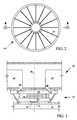
- FIG. 2is a simplified sectional plan view of test head 20 of FIG. 1 including a set of circuit boards 24 implementing channels 14 of FIG. 1.
- FIG. 3includes a partial sectional elevation view of test head 20 of FIG. 2 along with an elevation view of a probe card assembly 22 linking circuit boards 24 to bond pads on an IC die (DUT 12) formed on a wafer 13.
- DUT 12IC die
- FIGS. 2 and 3are intentionally not to scale. For example, those skilled in the art will appreciate, in particular, that test head 20 is much wider and taller relative to DUT 12 than is apparent from FIG. 3.
- probe assembly 22must not only route signals vertically between the bond pads of DUT 12 and circuit boards 24, it also must also route those signals horizontally.
- various probes, pogo pins, spring contacts, and vias within various layers forming probe card assembly 22move test signals vertically, while microstrip and stripline traces included within the various layers of the probe assembly 22 route those signals horizontally.
- Circuit boards 24are radially arrayed about a central vertical axis 26 passing through DUT 12 below the test head 20 so that all circuit boards 24 are substantially the same distance from DUT 12.
- Each circuit board 24is suitably arranged with its signal drivers and receivers mounted near the lower-most corner 28 of the circuit board nearest axis 26.
- One or more pogo pin connectors 30extending downward from corner 28 of each circuit board 24, suitably convey signals between circuit board 24 and probe card assembly 22.
- Probe card assembly 22which conveys signals between DUT 12 and the pogo pins 30 of circuit boards 24, includes a set of three vertically stacked layers.
- the primary layer of probe card assembly 22, a "probe card” 32,is mounted directly beneath probe head 20.
- Probe card 32provides points of contact on its upper surface for the pogo pin connectors 30 that act as input and/or output terminals for the tester channels 14 implemented by circuit boards 24.
- a "space transformer” 34includes a set of probes 36 oriented for contacting the bond pads on DUT 12.
- An “interposer” 38 positioned between probe card 32 and space transformer 34includes spring contacts 40 and 42 on its upper and lower surfaces for providing signal paths between contact pads on the facing surfaces of probe card 32 and space transformer 34.
- probe card assemblygenerally similar to probe card assembly 22 of FIG. 3 is described in more detail in PCT published application WO 96/15458, published May 23, 1996. It should be understood that while the preferred embodiment of the invention is illustrated herein in connection with the particular probe card assembly architecture described herein, the invention described herein is also applicable to other kinds of probe card assembly architectures.
- probe card assembly 22As thin as possible in the vertical direction, for example by providing probes 36 and connectors 40 and 42 that are as short as possible and by making probe card 32, space transformer 34 and interposer 38 as thin as possible.
- probe card assembly 22since there are structural limitations as to how small, thin and short we can make the various components of probe card assembly 22, signals must still travel a significant distance between pogo pins 30 and bond pads on the surface of DUT 12, and the impedance of the signal paths they follow distorts and attenuates those signals.
- the next step in reducing signal distortion and attenuation in the signal paths between IC bond pads and the tester channelshas been to carefully design those signal paths so as to minimize their impedances, particularly their shunt capacitance and series inductance.
- the capacitance of a signal pathdepends largely on its area, on its spacing and orientation relative to nearby ground and power planes, and on the dielectric constant of the material between the path and those ground and power planes.
- the capacitance of the signal paths through probe card assembly 22can be further reduced by appropriately choosing physical characteristics of probes 36, of contacts 40 and 42, and of the various traces and vias within the layers of probe card assembly 22 forming those signal paths.
- the series inductance of a signal pathis largely a function of its length, so when we reduce length of a signal path, we also reduce its inductance.
- other physical characteristics of a signal pathsuch as its width and its spacing relative to other conductors, can also influence path inductance.
- Probe card assembly designershave expended considerable effort to further reduce the inductance of signal paths through probe card assemblies by appropriately adjusting such physical characteristics of those paths.
- probe card assembly 22Although minimizing the signal path inductance and capacitances through probe card assembly 22 can generally increase bandwidth and reduce signal distortion, it is not possible to completely eliminate signal path inductance and capacitance. Likewise it is difficult to maintain a constant transmission line impedance through the probe structure. Thus some level of signal distortion and attenuation is therefore inevitable. Since distortion and attenuation generally increase with signal frequency, such signal distortion and attention provide a barrier to accurate high frequency testing.
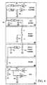
- the present inventionrepresents a next step in the process of improving the frequency response of probe card assembly 22, and to understand the invention, it is helpful to first model the signal path through probe card assembly 22, and the tester circuits and DUT it interconnects, with an equivalent circuit diagram. We can then study the effects on frequency response of various impedance values in the signal paths provided by a probe card assembly using a conventional circuit simulator programmed to simulate the frequency response of the equivalent circuit in a well-known manner.
- FIG. 4is an equivalent circuit diagram of the signal path between a driver 44 and a receiver 46 within a single tester channel 14 and a receiver 48 and driver 50 linked to a bond pad 52 within DUT 12.
- the DUT terminal being testedis a bi-directional input/output terminal, and therefore DUT 12 is depicted as including both a driver 50 for transmitting a DUT output signal from bond pad 50, and receiver 48 for receiving a DUT input signal arriving at bond pad 52.
- Tester channel 14is modeled as an ideal driver 44 linked through its output resistance Rl, a transmission line (if any) having a characteristic impedance Z0 1 , and pogo pin 30 to a pad 54 on the upper surface of probe card 32.
- probe card 32 of FIG. 3includes a microstrip trace of characteristic impedance Z0 3 on one of its surfaces for routing the signal horizontally from pad 54.
- Probe card 32may also include one or more vias for routing the signal vertically through probe card 32.
- the capacitances of such viasare included in C 1 and a capacitor C 2 .
- a viaalso has inductance and resistance, but since its capacitance predominates, it can be adequately modeled as a single shunt capacitor.
- Spring connectors 40 and 42 of interposer 38 of FIG. 3are modeled in FIG. 4 by a pair of series-connected inductors L 1 and L 2 .
- Interposer 38includes a vertical via linking connectors 40 and 42, and the capacitance of that via is suitably represented by a single shunt capacitor C 3 .
- Space transformer 34 of FIG. 3includes a microstrip trace for routing the signal horizontally across one of its surfaces, and that trace appears in FIG. 4 as characteristic impedance Z0 4 .
- a pair of shunt capacitors C 4 and C 5represent the capacitance of a contact pad on the upper surface of space transformer 34 and the capacitance of a via passing vertically through the space transformer 22.
- DUT 12will typically include an internal electrostatic protection device (ESD) linked to bond pad 52 for protecting DUT 12 from high-voltage electrostatic noise.
- ESDelectrostatic protection device
- the ESD device impedanceis represented in FIG. 4 by a shunt capacitor C 6 .
- the circuit formed by capacitors C1-C6, inductors L1-L3, resistors R1-R4, and transmission line impedances Z0 1 - Z0 4has a reactive impedance that can substantially attenuate and distort signals passing between driver 44 and receiver 48.
- the conventional approach to reducing the amount of signal distortion and attenuationhas been to minimize to the extent possible the various series inductances L1-L3 and shunt capacitances C1-C6 along the path. It is also a common practice to adjust all of resistances R1-R4 and characteristic impedances Z0 1 -Z0 4 to similar values (typically a standardized 50 Ohms in high-frequency applications).
- Such impedance matchingreduces signal reflections, thereby reducing the amount of distortion caused by the signal path.
- Table I belowlists impedance values of the various components FIG. 4 when impedances R 1 -R 3 are set to 50 Ohms and all inductances and capacitances have been set to typical minimum attainable values in accordance with conventional practice.
- Component Value R 1 -R 450 Ohms Z0 1 -Z0 4 50 Ohms C 1 0 . 4 pF C 2 0 .1 pF C 3 0.1 pF C 4 0.1 pF C 5 0 .1 pF C 6 0.05 pF L 1 0.8 nH L 2 0.8 nH L 3 0 . 8 nH
- FIG. 5illustrates the frequency response of the interconnect system model of FIG. 4 when components are set to the values indicated in Table I.
- FIG. 5plots signal attenuation as a function of frequency for signals passing from tester driver 44 to DUT receiver 48.
- the frequency response for signal passing in the other direction from driver 50 to receiver 46will be generally similar to that shown in FIG. 5 though there will be minor differences due to a lack of symmetry.
- the "optimal" frequency response characteristics for the interconnect system depicted in FIG. 4depends on the nature of the signals it is to convey. For example, when DUT 12 communicates via a high-frequency digital signal, we may want the interconnect system to pass high frequency signals, but we may not be too concerned about signal distortion, and therefore may be able to tolerate a reasonable amount of ripple in the passband. Under such circumstances we would want the interconnect system's passband to be as wide as possible while other characteristics of the interconnect frequency response are of lesser importance. On the other hand when DUT 12, for example, communicates via a low-frequency analog signal, we may want the interconnect system to convey low frequency signals with little distortion or noise, but we may want a wide bandwidth.
- the optimal frequency response for the interconnect systemmay include a passband that is as flat as possible but only as wide as needed to pass the highest frequency signal expected. We would also want all areas of the stopband to have maximal attenuation so as to block high frequency noise.
- the passband(usually defined as the frequency at which attenuation first falls by 3dB from its level at zero frequency) is about 2 GHz.
- the interconnect system performancemay be acceptable for signals of frequencies ranging between 0 and 2 GHz when a maximum 3dB attenuation is acceptable the interconnect system frequency response depicted by plot A would not be suitable for conveying signals of frequencies exceeding 2GHz.
- the passbandis not particularly flat at frequencies above 1 GHz. Since passband ripple distorts signals, then in applications where low distortion is required, the interconnect system frequency response depicted in plot A of FIG. 5 may not be suitable for conveying signals above 1 MHz.
- the stopbandhas several large peaks at frequencies above 2GHz and may therefore fail to sufficiently attenuate noise at those frequencies.
- the interconnect systemmay not be suitable in applications where we want to greatly attenuate all high frequency noise above a certain maximum signal frequency.
- the frequency response of a probe card assemblyis "optimized" for all applications by minimizing both its shunt capacitance and series inductance.
- interconnect system inductance and capacitancegenerally helps to increase bandwidth and reduce signal distortion, it is not true that setting system inductance and capacitance as low as possible necessarily optimizes the frequency response of the system for any particular application.
- system frequency responseis actually improved by increasing the inductance or capacitance of one or more of the elements forming the signal path through the probe card assembly above their minimum levels so as to appropriately adjust their values relative to one other.
- Table IIcompares typical impedance values of the elements of FIG. 4 set in accordance with prior art practice (Column A) to suitable impedance selected in accordance with the present invention (Column B) in an application where we want to maximize the passband power.
- Plot A of FIG. 5therefore also represents the frequency response of the probe card assembly equivalent circuit of FIG. 4 when values of its circuit components are set in accordance with prior art practice to typical minimum attainable values as listed in Table II, column A.
- Plot B of FIG. 5represents the frequency response of the probe card assembly equivalent circuit of FIG. 4 when values of its circuit components are set in accordance with the present invention as listed in Table II, column B.
- the impedance values of column B of Table IIwere not simply set to their lowest attainable values, but were instead carefully adjusted relative to one another and relative to the physical topology of the interconnect system to optimize the frequency response of the probe card assembly.
- the values listed in Table IIcolumn B were chosen to maximize the power conveyed in the passband - - that is, to maximize the amount of attenuation integrated over the full passband range.
- other impedance valuesmay be selected to optimize other characteristics or combinations of characteristics of frequency response for a given application. Thus for example, we may adjust impedance values to maximize bandwidth, to minimize ripple, to provide rapid fall off in the stop band, or some combination thereof.
- the interconnect systemcan be made to behave, for example, like a well-known, multi-pole "Butterworth” or “Chebyshev” filter. It is well understood how to adjust the component values of such filters in order to obtain a desired frequency response.
- the frequency response of an interconnect systemhas many characteristics and that its "optimal" frequency response is application-dependent.
- the appropriate values to which we adjust the various impedances along the signals paths of probe head assembly 22 should be adjusteddepends on which frequency response and impedance characteristics are most important for the particular application.
- capacitance valueswere chosen to maximize the passband power.
- other combinations of impedance valuescan optimize other characteristics of the interconnect system.
- the frequency response of the interconnect systemmay be desirable that the frequency response of the interconnect system have a "maximally flat" passband, having the least possible amount of ripple. In such case we will want to adjust the interconnect system component impedance values so that the system behaves like a Butterworth filter which does provide a maximally flat frequency response.
- inductive and capacitive componentscan be selected so that the interconnect system behaves as a form of the well-known, multiple-pole Chebyshev filter.
- the design of multi-pole Butterworth and Chebyshev filters,including appropriate choices for filter component values so as to optimize one or more combinations of characteristics of filter's frequency response,is well-known to those skilled in the art. See for example, pages 59-68 of the book Introduction to Radio Frequency Design by W. H. Hayward, published 1982 by Prentice-Hall, Inc..
- Driver and receiver impedances R1-R4, and the various transmission line impedances Z0 1 -Z0 4are typically set to similar values (e.g. , 50 Ohms) to prevent signal reflections which degrade system frequency response, and the values for these components were chosen in Table II, column B in order to conform with industry practice.
- similar valuese.g. , 50 Ohms
- pages 59-68 of the above- mentioned book Introduction to Radio Frequency Designillustrate how to adjust other filter component values to obtain Butterworth and Chebyshev filter frequency response behavior even when such resistive and characteristic impedances are mismatched.
Landscapes
- Physics & Mathematics (AREA)
- General Physics & Mathematics (AREA)
- Measuring Leads Or Probes (AREA)
- Testing Or Measuring Of Semiconductors Or The Like (AREA)
- Tests Of Electronic Circuits (AREA)
Description
| Component | Value |
| R1- | 50 Ohms |
| Z01- | 50 |
| C | |
| 1 | 0 . 4 |
| C | |
| 2 | 0 .1 pF |
| C3 | 0.1 pF |
| C4 | 0.1 |
| C | |
| 5 | 0 .1 pF |
| C6 | 0.05 pF |
| L1 | 0.8 nH |
| L2 | 0.8 |
| L | |
| 3 | 0 . 8 nH |
| Component | Impedance A | Impedance B |
| R1- | 50 | 50 Ohms |
| Z01- | 50 | 50 Ohms |
| C1 | 0.4 pF | 0.4 pF |
| C2 | 0.1 pF | 0.7 pF |
| C3 | 0.1 pF | 1.3 pF |
| C4 | 0.1 pF | 0.5 pF |
| C5 | 0.1 pF | 1.1 pF |
| C6 | 0.05 pF | 0.1 pF |
| L1 | 0.8 nH | 0.8 nH |
| L2 | 0.8 nH | 0.8 nH |
| L3 | 0.8 nH | 0.8 nH |
Claims (22)
- A signal path for linking a node (52) of an electronic device (12) to a terminal(30) of an electronic device tester (20), the signal path comprising:wherein said node (52), said probe (36) and said conductive path (32, 38, 34)have impedances sized relative to one another by choosing physical characteristics to substantially optimize a frequencyresponse characteristic of said signal path.a probe (36) for contacting said node; anda conductive path (32, 38, 34) on a probe card assembly (22) for linking saidprobe (36) to said terminal (30),
- The signal path in accordance with claim 1 wherein said impedances includeinductances in series with said signal path and capacitances shunting said signalpath.
- The signal path in accordance with claim 1 wherein said conductive pathcomprises:wherein said impedances include impedances of said node and of said first,second and third conductors.a probe card (32) including first conductors forming a first part of saidconductive path;a space transformer (34) including second conductors forming a second part ofsaid conductive path; andan interposer (38) including third conductors for conveying signals betweensaid first and second conductors,
- The signal path in accordance with claim 1 wherein said frequency responsecharacteristic is one of maximal passband width, maximal passband flatness andmaximal passband power.
- The signal path in accordance with claim 1 wherein said impedances are sizedrelative to one another so that said signal path forms a multiple-pole Butterworthfilter.
- The signal path in accordance with claim 1 wherein said impedances are sizedrelative to one another so that said signal path forms a multiple-pole Chebyshev filter.
- A signal path for linking a node (52) of an integrated circuit (IC) (12) to aterminal (30) of an IC tester (20), the signal path comprising:wherein said conductive pad and said conductive means have impedancessized by choosing physical characteristics relative to one another to substantially optimize a frequency responsecharacteristic of said signal path.a conductive pad (52) implemented on said IC and linked to said node;a probe (36) for contacting said conductive pad; andconductive means (32, 38, 34) on a probe card assembly (22) for linking saidprobe to said terminal,
- The signal path in accordance with claim 7 wherein said impedances includeinductances in series with said signal path and capacitances shunting said signalpath.
- The signal path in accordance with claim 7 wherein said conductive means(32) includes a printed circuit board via having a capacitance that is one of saidimpedances.
- The signal path in accordance with claim 7 wherein said conductive means(34) includes a trace having a characteristic impedance that is one of saidimpedances.
- The signal path in accordance with claim 7 wherein said conductive means(38) includes a spring contact (40, 42) having an inductance that is one of saidimpedances.
- The signal path in accordance with claim 7 wherein said conductive meanscomprises:a printed circuit board via having a capacitance that is one of said impedances,a trace having a characteristic impedance that is one of said impedances, anda spring contact having an inductance that is one of said impedances.
- The signal path in accordance with claim 7 wherein said conductive meanscomprises:wherein said impedances include impedances of said first, second and thirdconductors.a probe card (32) including first conductors forming a first part of said signalpath;a space transformer (34) including second conductors forming a second part ofsaid signal path; andan interposer (38) including a third conductor for conveying a signal betweensaid first and second conductors,
- The signal path in accordance with claim 7 wherein said frequency responsecharacteristic is one of maximal passband width, maximal passband flatness and amaximal passband power.
- The signal path in accordance with claim 7 wherein said impedances are sizedrelative to one another so that said interconnect system forms a multiple-poleButterworth filter.
- The signal path in accordance with claim 7 wherein said impedances are sizedrelative to one another so that said interconnect system forms a multiple-poleChebyshev filter.
- A method for sizing impedances of a signal path connecting a node (52) of anintegrated circuit (IC) (12) to a terminal (30) of an IC tester (20), wherein the signalpath comprises a bond pad (52) connected to said node, a probe (36) contacting saidbond pad, and conductive means (32, 38, 34) on a probe card assembly (22) linkingsaid probe to said terminal, the method comprising the step ofadjusting impedances of said bond pad, said probe, and said conductive meansrelative to one another by choosing physical characteristics so as to optimize a characteristic of a frequency response ofsaid signal path.
- The method in accordance with claim 17 wherein said characteristic of saidfrequency response is one of maximal passband width, maximal passband flatness andmaximal passband power.
- The method in accordance with claim 17 wherein said impedances are adjustedsuch that said signal path acts substantially. as a multiple-pole Butterworth filter.
- The method in accordance with claim 17 wherein said impedances are adjustedsuch that said signal path acts substantially as a multiple-pole Chebyshev filter.
- The signal path in accordance with claim 1 wherein the electronic device is anintegrated circuit (IC) comprising:wherein the probe (36) contacts said conductive pad; anda conductive pad (52) implemented on said IC (12) and linked to said node;
wherein said conductive pad, said probe, said terminal and said conductivepath have impedances sized relative to one another to substantially optimize afrequency response characteristic of said signal path, and
wherein said conductive path comprises a printed circuit board via having acapacitance that is one of said impedances. - The signal path in accordance with claim 1 wherein the electronic device is anintegrated circuit (IC),
wherein said node, said probe and said conductive path have impedances sizedrelative to one another to substantially optimize a frequency characteristic of saidsignal path, and
wherein said conductive path comprises a printed circuit board via having acapacitance that is one of said impedances.
Applications Claiming Priority (3)
| Application Number | Priority Date | Filing Date | Title |
|---|---|---|---|
| US258186 | 1999-02-25 | ||
| US09/258,186US6218910B1 (en) | 1999-02-25 | 1999-02-25 | High bandwidth passive integrated circuit tester probe card assembly |
| PCT/US2000/004674WO2000050905A1 (en) | 1999-02-25 | 2000-02-23 | High bandwidth passive integrated circuit tester probe card assembly |
Publications (2)
| Publication Number | Publication Date |
|---|---|
| EP1159624A1 EP1159624A1 (en) | 2001-12-05 |
| EP1159624B1true EP1159624B1 (en) | 2004-01-02 |
Family
ID=22979472
Family Applications (1)
| Application Number | Title | Priority Date | Filing Date |
|---|---|---|---|
| EP00914677AExpired - LifetimeEP1159624B1 (en) | 1999-02-25 | 2000-02-23 | High bandwidth passive integrated circuit tester probe card assembly |
Country Status (8)
| Country | Link |
|---|---|
| US (5) | US6218910B1 (en) |
| EP (1) | EP1159624B1 (en) |
| JP (2) | JP2002538435A (en) |
| KR (3) | KR100793501B1 (en) |
| AU (1) | AU3603400A (en) |
| DE (1) | DE60007516T2 (en) |
| TW (1) | TW514733B (en) |
| WO (1) | WO2000050905A1 (en) |
Families Citing this family (135)
| Publication number | Priority date | Publication date | Assignee | Title |
|---|---|---|---|---|
| US20020053734A1 (en) | 1993-11-16 | 2002-05-09 | Formfactor, Inc. | Probe card assembly and kit, and methods of making same |
| US6232789B1 (en)* | 1997-05-28 | 2001-05-15 | Cascade Microtech, Inc. | Probe holder for low current measurements |
| US5729150A (en)* | 1995-12-01 | 1998-03-17 | Cascade Microtech, Inc. | Low-current probe card with reduced triboelectric current generating cables |
| US5914613A (en) | 1996-08-08 | 1999-06-22 | Cascade Microtech, Inc. | Membrane probing system with local contact scrub |
| US6034533A (en)* | 1997-06-10 | 2000-03-07 | Tervo; Paul A. | Low-current pogo probe card |
| US6256882B1 (en) | 1998-07-14 | 2001-07-10 | Cascade Microtech, Inc. | Membrane probing system |
| US6218910B1 (en)* | 1999-02-25 | 2001-04-17 | Formfactor, Inc. | High bandwidth passive integrated circuit tester probe card assembly |
| US6538538B2 (en) | 1999-02-25 | 2003-03-25 | Formfactor, Inc. | High frequency printed circuit board via |
| US7349223B2 (en) | 2000-05-23 | 2008-03-25 | Nanonexus, Inc. | Enhanced compliant probe card systems having improved planarity |
| US6812718B1 (en)* | 1999-05-27 | 2004-11-02 | Nanonexus, Inc. | Massively parallel interface for electronic circuits |
| US6799976B1 (en)* | 1999-07-28 | 2004-10-05 | Nanonexus, Inc. | Construction structures and manufacturing processes for integrated circuit wafer probe card assemblies |
| US7382142B2 (en) | 2000-05-23 | 2008-06-03 | Nanonexus, Inc. | High density interconnect system having rapid fabrication cycle |
| US7247035B2 (en)* | 2000-06-20 | 2007-07-24 | Nanonexus, Inc. | Enhanced stress metal spring contactor |
| US6578264B1 (en) | 1999-06-04 | 2003-06-17 | Cascade Microtech, Inc. | Method for constructing a membrane probe using a depression |
| US6392428B1 (en)* | 1999-11-16 | 2002-05-21 | Eaglestone Partners I, Llc | Wafer level interposer |
| AU2001243200A1 (en)* | 2000-02-22 | 2001-09-03 | Don Mccord | Method and system for wafer and device-level testing of an integrated circuit |
| US6838890B2 (en) | 2000-02-25 | 2005-01-04 | Cascade Microtech, Inc. | Membrane probing system |
| US6724209B1 (en)* | 2000-04-13 | 2004-04-20 | Ralph G. Whitten | Method for testing signal paths between an integrated circuit wafer and a wafer tester |
| JP2001296335A (en)* | 2000-04-14 | 2001-10-26 | Nec Corp | Method and apparatus for inspection of semiconductor device |
| US7952373B2 (en) | 2000-05-23 | 2011-05-31 | Verigy (Singapore) Pte. Ltd. | Construction structures and manufacturing processes for integrated circuit wafer probe card assemblies |
| US20050068054A1 (en)* | 2000-05-23 | 2005-03-31 | Sammy Mok | Standardized layout patterns and routing structures for integrated circuit wafer probe card assemblies |
| US7579848B2 (en) | 2000-05-23 | 2009-08-25 | Nanonexus, Inc. | High density interconnect system for IC packages and interconnect assemblies |
| US6812048B1 (en)* | 2000-07-31 | 2004-11-02 | Eaglestone Partners I, Llc | Method for manufacturing a wafer-interposer assembly |
| US6537831B1 (en) | 2000-07-31 | 2003-03-25 | Eaglestone Partners I, Llc | Method for selecting components for a matched set using a multi wafer interposer |
| US6970005B2 (en)* | 2000-08-24 | 2005-11-29 | Texas Instruments Incorporated | Multiple-chip probe and universal tester contact assemblage |
| US6927591B2 (en)* | 2000-09-22 | 2005-08-09 | Mccord Don | Method and system for wafer and device level testing of an integrated circuit |
| US6815712B1 (en) | 2000-10-02 | 2004-11-09 | Eaglestone Partners I, Llc | Method for selecting components for a matched set from a wafer-interposer assembly |
| US6686657B1 (en)* | 2000-11-07 | 2004-02-03 | Eaglestone Partners I, Llc | Interposer for improved handling of semiconductor wafers and method of use of same |
| DE20114544U1 (en) | 2000-12-04 | 2002-02-21 | Cascade Microtech, Inc., Beaverton, Oreg. | wafer probe |
| US6529022B2 (en)* | 2000-12-15 | 2003-03-04 | Eaglestone Pareners I, Llc | Wafer testing interposer for a conventional package |
| US6524885B2 (en) | 2000-12-15 | 2003-02-25 | Eaglestone Partners I, Llc | Method, apparatus and system for building an interposer onto a semiconductor wafer using laser techniques |
| FR2819678B1 (en)* | 2001-01-12 | 2003-04-11 | Sagem | FILTERING CIRCUIT, AND POWER SUPPLY DEVICE PROVIDED WITH SUCH A FILTERING CIRCUIT |
| US6673653B2 (en) | 2001-02-23 | 2004-01-06 | Eaglestone Partners I, Llc | Wafer-interposer using a ceramic substrate |
| US6729019B2 (en)* | 2001-07-11 | 2004-05-04 | Formfactor, Inc. | Method of manufacturing a probe card |
| EP1407280B1 (en)* | 2001-07-11 | 2005-11-23 | Formfactor, Inc. | Method of manufacturing a probe card |
| JP2003043066A (en)* | 2001-07-26 | 2003-02-13 | Hoya Corp | Contact probe member and its production method |
| US6570397B2 (en) | 2001-08-07 | 2003-05-27 | Agilent Technologies, Inc. | Timing calibration and timing calibration verification of electronic circuit testers |
| US7355420B2 (en) | 2001-08-21 | 2008-04-08 | Cascade Microtech, Inc. | Membrane probing system |
| WO2003018865A1 (en)* | 2001-08-24 | 2003-03-06 | Nanonexus, Inc. | Method and apparatus for producing uniform isotropic stresses in a sputtered film |
| US6714828B2 (en) | 2001-09-17 | 2004-03-30 | Formfactor, Inc. | Method and system for designing a probe card |
| US6816031B1 (en) | 2001-12-04 | 2004-11-09 | Formfactor, Inc. | Adjustable delay transmission line |
| US20060053625A1 (en)* | 2002-05-07 | 2006-03-16 | Microfabrica Inc. | Microprobe tips and methods for making |
| US7531077B2 (en) | 2003-02-04 | 2009-05-12 | Microfabrica Inc. | Electrochemical fabrication process for forming multilayer multimaterial microprobe structures |
| US7412767B2 (en)* | 2003-02-04 | 2008-08-19 | Microfabrica, Inc. | Microprobe tips and methods for making |
| US20060006888A1 (en)* | 2003-02-04 | 2006-01-12 | Microfabrica Inc. | Electrochemically fabricated microprobes |
| US7265565B2 (en) | 2003-02-04 | 2007-09-04 | Microfabrica Inc. | Cantilever microprobes for contacting electronic components and methods for making such probes |
| US20050184748A1 (en)* | 2003-02-04 | 2005-08-25 | Microfabrica Inc. | Pin-type probes for contacting electronic circuits and methods for making such probes |
| US20060238209A1 (en)* | 2002-05-07 | 2006-10-26 | Microfabrica Inc. | Vertical microprobes for contacting electronic components and method for making such probes |
| US7273812B2 (en)* | 2002-05-07 | 2007-09-25 | Microfabrica Inc. | Microprobe tips and methods for making |
| US20060051948A1 (en)* | 2003-02-04 | 2006-03-09 | Microfabrica Inc. | Microprobe tips and methods for making |
| US20050104609A1 (en)* | 2003-02-04 | 2005-05-19 | Microfabrica Inc. | Microprobe tips and methods for making |
| US7363705B2 (en)* | 2003-02-04 | 2008-04-29 | Microfabrica, Inc. | Method of making a contact |
| US7640651B2 (en)* | 2003-12-31 | 2010-01-05 | Microfabrica Inc. | Fabrication process for co-fabricating multilayer probe array and a space transformer |
| US6911835B2 (en)* | 2002-05-08 | 2005-06-28 | Formfactor, Inc. | High performance probe system |
| US6798225B2 (en)* | 2002-05-08 | 2004-09-28 | Formfactor, Inc. | Tester channel to multiple IC terminals |
| US6965244B2 (en)* | 2002-05-08 | 2005-11-15 | Formfactor, Inc. | High performance probe system |
| US6784674B2 (en)* | 2002-05-08 | 2004-08-31 | Formfactor, Inc. | Test signal distribution system for IC tester |
| KR100864916B1 (en) | 2002-05-23 | 2008-10-22 | 캐스케이드 마이크로테크 인코포레이티드 | Probes for Testing Devices Under Test |
| US7102367B2 (en)* | 2002-07-23 | 2006-09-05 | Fujitsu Limited | Probe card and testing method of semiconductor chip, capacitor and manufacturing method thereof |
| US6724205B1 (en)* | 2002-11-13 | 2004-04-20 | Cascade Microtech, Inc. | Probe for combined signals |
| US6956448B1 (en) | 2002-12-17 | 2005-10-18 | Itt Manufacturing Enterprises, Inc. | Electromagnetic energy probe with integral impedance matching |
| US20080157793A1 (en)* | 2003-02-04 | 2008-07-03 | Microfabrica Inc. | Vertical Microprobes for Contacting Electronic Components and Method for Making Such Probes |
| US20080211524A1 (en)* | 2003-02-04 | 2008-09-04 | Microfabrica Inc. | Electrochemically Fabricated Microprobes |
| US10416192B2 (en) | 2003-02-04 | 2019-09-17 | Microfabrica Inc. | Cantilever microprobes for contacting electronic components |
| US8613846B2 (en)* | 2003-02-04 | 2013-12-24 | Microfabrica Inc. | Multi-layer, multi-material fabrication methods for producing micro-scale and millimeter-scale devices with enhanced electrical and/or mechanical properties |
| US7567089B2 (en)* | 2003-02-04 | 2009-07-28 | Microfabrica Inc. | Two-part microprobes for contacting electronic components and methods for making such probes |
| US9244101B2 (en)* | 2003-02-04 | 2016-01-26 | University Of Southern California | Electrochemical fabrication process for forming multilayer multimaterial microprobe structures |
| US9671429B2 (en) | 2003-05-07 | 2017-06-06 | University Of Southern California | Multi-layer, multi-material micro-scale and millimeter-scale devices with enhanced electrical and/or mechanical properties |
| US7057404B2 (en) | 2003-05-23 | 2006-06-06 | Sharp Laboratories Of America, Inc. | Shielded probe for testing a device under test |
| NL1023597C2 (en)* | 2003-06-04 | 2004-12-07 | Tu Delft | Loss compensating circuit. |
| US7276895B2 (en)* | 2003-10-03 | 2007-10-02 | Intest Corporation | Adjustable test head docking apparatus |
| WO2005065258A2 (en) | 2003-12-24 | 2005-07-21 | Cascade Microtech, Inc. | Active wafer probe |
| US10641792B2 (en) | 2003-12-31 | 2020-05-05 | University Of Southern California | Multi-layer, multi-material micro-scale and millimeter-scale devices with enhanced electrical and/or mechanical properties |
| US20080108221A1 (en)* | 2003-12-31 | 2008-05-08 | Microfabrica Inc. | Microprobe Tips and Methods for Making |
| US7388424B2 (en) | 2004-04-07 | 2008-06-17 | Formfactor, Inc. | Apparatus for providing a high frequency loop back with a DC path for a parametric test |
| US10188973B2 (en) | 2004-04-08 | 2019-01-29 | Research Triangle Institute | Apparatus and method using an electric field for creating uniform nanofiber patterns on nonconductive materials to enhance filtration and for embedment of fibers into materials for other applications |
| US7071720B2 (en)* | 2004-06-10 | 2006-07-04 | International Business Machines Corporation | Method and apparatus for managing aligning and coupling of a land grid array interposer for a field replacement unit |
| KR101157449B1 (en) | 2004-07-07 | 2012-06-22 | 캐스케이드 마이크로테크 인코포레이티드 | Probe head having a membrane suspended probe |
| US20060030179A1 (en)* | 2004-08-05 | 2006-02-09 | Palo Alto Research Center, Incorporated | Transmission-line spring structure |
| US6956389B1 (en)* | 2004-08-16 | 2005-10-18 | Jem America Corporation | Highly resilient cantilever spring probe for testing ICs |
| EP1789812A2 (en) | 2004-09-13 | 2007-05-30 | Cascade Microtech, Inc. | Double sided probing structures |
| DE102004050615A1 (en)* | 2004-10-18 | 2006-04-27 | Siemens Ag | Device for testing processing electronics |
| US7088118B2 (en)* | 2004-12-15 | 2006-08-08 | Chipmos Technologies (Bermuda) Ltd. | Modularized probe card for high frequency probing |
| US7414418B2 (en)* | 2005-01-07 | 2008-08-19 | Formfactor, Inc. | Method and apparatus for increasing operating frequency of a system for testing electronic devices |
| US7535247B2 (en) | 2005-01-31 | 2009-05-19 | Cascade Microtech, Inc. | Interface for testing semiconductors |
| US7656172B2 (en) | 2005-01-31 | 2010-02-02 | Cascade Microtech, Inc. | System for testing semiconductors |
| US7449899B2 (en) | 2005-06-08 | 2008-11-11 | Cascade Microtech, Inc. | Probe for high frequency signals |
| JP5080459B2 (en) | 2005-06-13 | 2012-11-21 | カスケード マイクロテック インコーポレイテッド | Wideband active / passive differential signal probe |
| CN100424512C (en)* | 2005-08-25 | 2008-10-08 | 南茂科技股份有限公司 | Modular high-frequency probe card |
| US7498883B2 (en)* | 2005-10-07 | 2009-03-03 | University Of Rochester | Distributed amplifier with built-in filtering functions |
| KR101025895B1 (en)* | 2006-06-08 | 2011-03-30 | 니혼 하츠쵸 가부시키가이샤 | Probe card |
| US7609077B2 (en) | 2006-06-09 | 2009-10-27 | Cascade Microtech, Inc. | Differential signal probe with integral balun |
| US7723999B2 (en) | 2006-06-12 | 2010-05-25 | Cascade Microtech, Inc. | Calibration structures for differential signal probing |
| US7764072B2 (en) | 2006-06-12 | 2010-07-27 | Cascade Microtech, Inc. | Differential signal probing system |
| US7403028B2 (en) | 2006-06-12 | 2008-07-22 | Cascade Microtech, Inc. | Test structure and probe for differential signals |
| US7443186B2 (en) | 2006-06-12 | 2008-10-28 | Cascade Microtech, Inc. | On-wafer test structures for differential signals |
| US7629804B2 (en)* | 2006-08-04 | 2009-12-08 | Vertical Test Inc. | Probe head assembly for use in testing multiple wafer die |
| US7659790B2 (en)* | 2006-08-22 | 2010-02-09 | Lecroy Corporation | High speed signal transmission line having reduced thickness regions |
| US7378832B2 (en)* | 2006-08-22 | 2008-05-27 | Lecroy Corporation | Probing high-frequency signals |
| US20090027071A1 (en)* | 2007-07-23 | 2009-01-29 | Finsar Corporation | Probe tap |
| US7876114B2 (en) | 2007-08-08 | 2011-01-25 | Cascade Microtech, Inc. | Differential waveguide probe |
| KR20090082783A (en)* | 2008-01-28 | 2009-07-31 | 삼성전자주식회사 | Prove card assembly for electrical die sorting process |
| US8056025B1 (en)* | 2008-02-21 | 2011-11-08 | Altera Corporation | Integration of open space/dummy metal at CAD for physical debug of new silicon |
| US8033012B2 (en)* | 2008-03-07 | 2011-10-11 | Taiwan Semiconductor Manufacturing Co., Ltd. | Method for fabricating a semiconductor test probe card space transformer |
| US7924035B2 (en)* | 2008-07-15 | 2011-04-12 | Formfactor, Inc. | Probe card assembly for electronic device testing with DC test resource sharing |
| US7888957B2 (en) | 2008-10-06 | 2011-02-15 | Cascade Microtech, Inc. | Probing apparatus with impedance optimized interface |
| WO2010048971A1 (en)* | 2008-10-30 | 2010-05-06 | Verigy (Singapore) Pte., Ltd. | Test arrangement, pogo-pin and method for testing a device under test |
| US8410806B2 (en) | 2008-11-21 | 2013-04-02 | Cascade Microtech, Inc. | Replaceable coupon for a probing apparatus |
| US8134380B2 (en)* | 2008-11-26 | 2012-03-13 | Taiwan Semiconductor Manufacturing Company, Ltd. | Test probe structure |
| JP5228925B2 (en)* | 2009-01-09 | 2013-07-03 | 三菱電機株式会社 | High frequency contactor |
| US8098076B2 (en)* | 2009-04-01 | 2012-01-17 | Formfactor, Inc. | Method and apparatus for terminating a test signal applied to multiple semiconductor loads under test |
| EP2414809B1 (en) | 2009-04-03 | 2019-08-14 | 3M Innovative Properties Company | Microorganism concentration process and device |
| CN102004173B (en)* | 2009-09-01 | 2014-02-19 | 鸿富锦精密工业(深圳)有限公司 | probe |
| US8638114B2 (en)* | 2009-12-08 | 2014-01-28 | Qualcomm Incorporated | Transformer within wafer test probe |
| US20110147568A1 (en)* | 2009-12-18 | 2011-06-23 | Irvine Sensors Corporation | High density array module and connector |
| IT1403475B1 (en)* | 2010-12-20 | 2013-10-17 | St Microelectronics Srl | CONNECTION STRUCTURE FOR AN INTEGRATED CIRCUIT WITH CAPACITIVE FUNCTION |
| JP5492230B2 (en)* | 2012-01-20 | 2014-05-14 | 株式会社日本マイクロニクス | Inspection device |
| CN103454571B (en)* | 2012-05-30 | 2017-10-27 | 富泰华工业(深圳)有限公司 | Test system, method of testing and the test equipment using the test system |
| US9470753B2 (en) | 2012-11-07 | 2016-10-18 | Cascade Microtech, Inc. | Systems and methods for testing electronic devices that include low power output drivers |
| WO2014094819A1 (en)* | 2012-12-17 | 2014-06-26 | Advantest (Singapore) Pte. Ltd. | Rf probe |
| US10067163B2 (en)* | 2012-12-26 | 2018-09-04 | Mpi Corporation | Probe card capable of transmitting high-frequency signals |
| TWI471570B (en)* | 2012-12-26 | 2015-02-01 | Mpi Corp | High frequency probe card |
| GB2511528A (en) | 2013-03-06 | 2014-09-10 | Speciality Fibres And Materials Ltd | Absorbent materials |
| TWI661206B (en)* | 2018-01-19 | 2019-06-01 | 新加坡商美亞國際電子有限公司 | Printed circuit board for electrical testing |
| EP3807656B1 (en) | 2018-06-14 | 2024-08-07 | FormFactor, Inc. | Electrical test probes having decoupled electrical and mechanical design |
| WO2020033335A1 (en)* | 2018-08-06 | 2020-02-13 | Testmetrix, Inc. | Apparatus and method for testing semiconductor devices |
| US20220137132A1 (en)* | 2018-08-06 | 2022-05-05 | Testmetrix, Inc. | Apparatus and Method for Testing Semiconductor Devices |
| US11262383B1 (en) | 2018-09-26 | 2022-03-01 | Microfabrica Inc. | Probes having improved mechanical and/or electrical properties for making contact between electronic circuit elements and methods for making |
| US12078657B2 (en) | 2019-12-31 | 2024-09-03 | Microfabrica Inc. | Compliant pin probes with extension springs, methods for making, and methods for using |
| US11573264B2 (en)* | 2019-04-10 | 2023-02-07 | Mediatek Inc. | Device for testing chip or die with better system IR drop |
| EP3859359B8 (en)* | 2020-01-28 | 2024-04-10 | Rohde & Schwarz GmbH & Co. KG | Signal analysis method and test system |
| US11215663B2 (en)* | 2020-04-28 | 2022-01-04 | Reedholm Systems Corporation | Systems and methods for parametric testing |
| WO2022217046A1 (en)* | 2021-04-08 | 2022-10-13 | Tektronix, Inc. | Precision, high bandwidth, switching attenuator |
| US11782154B1 (en) | 2021-11-01 | 2023-10-10 | National Technology & Engineering Solutions Of Sandia, Llc | Terrain-aided position determination using range angle radar altimetry |
| EP4533106A1 (en)* | 2022-06-03 | 2025-04-09 | FormFactor, Inc. | Abbreviated loopback attenuation |
Family Cites Families (39)
| Publication number | Priority date | Publication date | Assignee | Title |
|---|---|---|---|---|
| US4354268A (en)* | 1980-04-03 | 1982-10-12 | Santek, Inc. | Intelligent test head for automatic test system |
| US4342013A (en) | 1980-08-25 | 1982-07-27 | Pilgrim Electric Co. | Bidirectional power line filter |
| JPS5873881A (en) | 1981-10-29 | 1983-05-04 | Advantest Corp | Ic tester |
| US4472725A (en) | 1982-02-01 | 1984-09-18 | Century Iii Electronics Inc. | LC Delay line for feedforward amplifier |
| US4616178A (en)* | 1982-05-27 | 1986-10-07 | Harris Corporation | Pulsed linear integrated circuit tester |
| US4837622A (en)* | 1985-05-10 | 1989-06-06 | Micro-Probe, Inc. | High density probe card |
| JPS62130367A (en)* | 1985-12-03 | 1987-06-12 | Hitachi Electronics Eng Co Ltd | Electronic device drive circuit |
| US4928062A (en)* | 1988-01-20 | 1990-05-22 | Texas Instruments Incorporated | Loading and accurate measurement of integrated dynamic parameters at point of contact in automatic device handlers |
| US5012213A (en) | 1989-12-19 | 1991-04-30 | Motorola, Inc. | Providing a PGA package with a low reflection line |
| US5090118A (en)* | 1990-07-31 | 1992-02-25 | Texas Instruments Incorporated | High performance test head and method of making |
| JPH04107940A (en) | 1990-08-29 | 1992-04-09 | Hitachi Ltd | Semiconductor devices and their components |
| US5172051A (en) | 1991-04-24 | 1992-12-15 | Hewlett-Packard Company | Wide bandwidth passive probe |
| US5574382A (en)* | 1991-09-17 | 1996-11-12 | Japan Synthetic Rubber Co., Ltd. | Inspection electrode unit for printed wiring board |
| GB2263980B (en)* | 1992-02-07 | 1996-04-10 | Marconi Gec Ltd | Apparatus and method for testing bare dies |
| US5182220A (en) | 1992-04-02 | 1993-01-26 | United Microelectronics Corporation | CMOS on-chip ESD protection circuit and semiconductor structure |
| US5270673A (en) | 1992-07-24 | 1993-12-14 | Hewlett-Packard Company | Surface mount microcircuit hybrid |
| US5424693A (en) | 1993-01-13 | 1995-06-13 | Industrial Technology Research Institute | Surface mountable microwave IC package |
| US5309019A (en) | 1993-02-26 | 1994-05-03 | Motorola, Inc. | Low inductance lead frame for a semiconductor package |
| US5536906A (en) | 1993-07-23 | 1996-07-16 | Texas Instruments Incorporated | Package for integrated circuits |
| JPH0799220A (en)* | 1993-08-04 | 1995-04-11 | Tokyo Electron Ltd | Probe card, coaxial probe needle for probe card and their production |
| JPH07321168A (en)* | 1994-05-27 | 1995-12-08 | Tokyo Electron Ltd | Probe card |
| US5521406A (en) | 1994-08-31 | 1996-05-28 | Texas Instruments Incorporated | Integrated circuit with improved thermal impedance |
| JPH08139142A (en)* | 1994-11-09 | 1996-05-31 | Tokyo Electron Ltd | Probe unit |
| KR100324059B1 (en)* | 1994-11-15 | 2002-04-17 | 이고르 와이. 칸드로스 | Interconnection Elements for Microelectronic Components |
| US5546405A (en)* | 1995-07-17 | 1996-08-13 | Advanced Micro Devices, Inc. | Debug apparatus for an automated semiconductor testing system |
| US5642054A (en)* | 1995-08-08 | 1997-06-24 | Hughes Aircraft Company | Active circuit multi-port membrane probe for full wafer testing |
| US5744869A (en) | 1995-12-05 | 1998-04-28 | Motorola, Inc. | Apparatus for mounting a flip-chip semiconductor device |
| JP3634074B2 (en)* | 1996-06-28 | 2005-03-30 | 日本発条株式会社 | Conductive contact |
| JPH10123215A (en)* | 1996-10-21 | 1998-05-15 | Toshiba Microelectron Corp | Semiconductor integrated circuit |
| US5917220A (en) | 1996-12-31 | 1999-06-29 | Stmicroelectronics, Inc. | Integrated circuit with improved overvoltage protection |
| US5901022A (en) | 1997-02-24 | 1999-05-04 | Industrial Technology Research Inst. | Charged device mode ESD protection circuit |
| JP2000510653A (en) | 1997-04-16 | 2000-08-15 | ザ ボード オブ トラスティーズ オブ ザ リーランド スタンフォード ジュニア ユニバーシティ | Distributed ESD protection device for high-speed integrated circuits |
| JPH10300778A (en)* | 1997-04-24 | 1998-11-13 | Kiyandotsukusu Syst:Kk | Method for measuring high frequency characteristics of high frequency device |
| US5869898A (en) | 1997-04-25 | 1999-02-09 | Nec Corporation | Lead-frame having interdigitated signal and ground leads with high frequency leads positioned adjacent a corner and shielded by ground leads on either side thereof |
| JP3378259B2 (en) | 1997-05-15 | 2003-02-17 | フォームファクター,インコーポレイテッド | How to create a contact structure |
| US6008533A (en) | 1997-12-08 | 1999-12-28 | Micron Technology, Inc. | Controlling impedances of an integrated circuit |
| US6208225B1 (en) | 1999-02-25 | 2001-03-27 | Formfactor, Inc. | Filter structures for integrated circuit interfaces |
| US6448865B1 (en) | 1999-02-25 | 2002-09-10 | Formfactor, Inc. | Integrated circuit interconnect system |
| US6218910B1 (en)* | 1999-02-25 | 2001-04-17 | Formfactor, Inc. | High bandwidth passive integrated circuit tester probe card assembly |
- 1999
- 1999-02-25USUS09/258,186patent/US6218910B1/ennot_activeExpired - Lifetime
- 2000
- 2000-02-22TWTW089103077Apatent/TW514733B/ennot_activeIP Right Cessation
- 2000-02-23DEDE60007516Tpatent/DE60007516T2/ennot_activeExpired - Lifetime
- 2000-02-23JPJP2000601449Apatent/JP2002538435A/enactivePending
- 2000-02-23KRKR1020077006242Apatent/KR100793501B1/ennot_activeExpired - Fee Related
- 2000-02-23WOPCT/US2000/004674patent/WO2000050905A1/enactiveIP Right Grant
- 2000-02-23AUAU36034/00Apatent/AU3603400A/ennot_activeAbandoned
- 2000-02-23KRKR1020067019906Apatent/KR100757578B1/ennot_activeExpired - Fee Related
- 2000-02-23EPEP00914677Apatent/EP1159624B1/ennot_activeExpired - Lifetime
- 2000-02-23KRKR1020017010746Apatent/KR100757577B1/ennot_activeExpired - Fee Related
- 2001
- 2001-03-13USUS09/805,668patent/US6501343B2/ennot_activeExpired - Fee Related
- 2002
- 2002-10-31USUS10/286,062patent/US6686754B2/ennot_activeExpired - Fee Related
- 2003
- 2003-12-29USUS10/749,358patent/US6917210B2/ennot_activeExpired - Fee Related
- 2005
- 2005-07-12USUS11/180,247patent/US20110115512A1/ennot_activeAbandoned
- 2007
- 2007-02-22JPJP2007043029Apatent/JP2007178440A/enactivePending
Also Published As
| Publication number | Publication date |
|---|---|
| KR100757578B1 (en) | 2007-09-10 |
| JP2007178440A (en) | 2007-07-12 |
| KR100757577B1 (en) | 2007-09-10 |
| WO2000050905A1 (en) | 2000-08-31 |
| US6917210B2 (en) | 2005-07-12 |
| TW514733B (en) | 2002-12-21 |
| AU3603400A (en) | 2000-09-14 |
| US20110115512A1 (en) | 2011-05-19 |
| KR20070038181A (en) | 2007-04-09 |
| US6218910B1 (en) | 2001-04-17 |
| US20030067316A1 (en) | 2003-04-10 |
| US6501343B2 (en) | 2002-12-31 |
| US6686754B2 (en) | 2004-02-03 |
| US20040140822A1 (en) | 2004-07-22 |
| JP2002538435A (en) | 2002-11-12 |
| EP1159624A1 (en) | 2001-12-05 |
| US20010035800A1 (en) | 2001-11-01 |
| KR100793501B1 (en) | 2008-01-14 |
| DE60007516T2 (en) | 2004-09-23 |
| DE60007516D1 (en) | 2004-02-05 |
| KR20060106938A (en) | 2006-10-12 |
| KR20010102357A (en) | 2001-11-15 |
Similar Documents
| Publication | Publication Date | Title |
|---|---|---|
| EP1159624B1 (en) | High bandwidth passive integrated circuit tester probe card assembly | |
| US6208225B1 (en) | Filter structures for integrated circuit interfaces | |
| US6822529B2 (en) | Integrated circuit interconnect system | |
| US6784677B2 (en) | Closed-grid bus architecture for wafer interconnect structure | |
| US6215320B1 (en) | High density printed circuit board | |
| US20030210067A1 (en) | Test signal distribution system for IC tester | |
| WO1999041812A1 (en) | Ic socket | |
| US7388424B2 (en) | Apparatus for providing a high frequency loop back with a DC path for a parametric test | |
| US5311122A (en) | RF test equipment and wire bond interface circuit |
Legal Events
| Date | Code | Title | Description |
|---|---|---|---|
| PUAI | Public reference made under article 153(3) epc to a published international application that has entered the european phase | Free format text:ORIGINAL CODE: 0009012 | |
| 17P | Request for examination filed | Effective date:20010925 | |
| AK | Designated contracting states | Kind code of ref document:A1 Designated state(s):AT BE CH CY DE DK ES FI FR GB GR IE IT LI LU MC NL PT SE | |
| AX | Request for extension of the european patent | Free format text:AL;LT;LV;MK;RO;SI | |
| RAP1 | Party data changed (applicant data changed or rights of an application transferred) | Owner name:FORMFACTOR, INC. | |
| 17Q | First examination report despatched | Effective date:20020114 | |
| GRAH | Despatch of communication of intention to grant a patent | Free format text:ORIGINAL CODE: EPIDOS IGRA | |
| GRAS | Grant fee paid | Free format text:ORIGINAL CODE: EPIDOSNIGR3 | |
| GRAA | (expected) grant | Free format text:ORIGINAL CODE: 0009210 | |
| AK | Designated contracting states | Kind code of ref document:B1 Designated state(s):DE FR GB IT | |
| PG25 | Lapsed in a contracting state [announced via postgrant information from national office to epo] | Ref country code:IT Free format text:LAPSE BECAUSE OF FAILURE TO SUBMIT A TRANSLATION OF THE DESCRIPTION OR TO PAY THE FEE WITHIN THE PRESCRIBED TIME-LIMIT;WARNING: LAPSES OF ITALIAN PATENTS WITH EFFECTIVE DATE BEFORE 2007 MAY HAVE OCCURRED AT ANY TIME BEFORE 2007. THE CORRECT EFFECTIVE DATE MAY BE DIFFERENT FROM THE ONE RECORDED. Effective date:20040102 | |
| REG | Reference to a national code | Ref country code:GB Ref legal event code:FG4D | |
| REG | Reference to a national code | Ref country code:IE Ref legal event code:FG4D | |
| REF | Corresponds to: | Ref document number:60007516 Country of ref document:DE Date of ref document:20040205 Kind code of ref document:P | |
| PGFP | Annual fee paid to national office [announced via postgrant information from national office to epo] | Ref country code:FR Payment date:20040226 Year of fee payment:5 | |
| PG25 | Lapsed in a contracting state [announced via postgrant information from national office to epo] | Ref country code:GB Free format text:LAPSE BECAUSE OF NON-PAYMENT OF DUE FEES Effective date:20040402 | |
| LTIE | Lt: invalidation of european patent or patent extension | Effective date:20040102 | |
| ET | Fr: translation filed | ||
| PLBE | No opposition filed within time limit | Free format text:ORIGINAL CODE: 0009261 | |
| STAA | Information on the status of an ep patent application or granted ep patent | Free format text:STATUS: NO OPPOSITION FILED WITHIN TIME LIMIT | |
| REG | Reference to a national code | Ref country code:IE Ref legal event code:MM4A | |
| GBPC | Gb: european patent ceased through non-payment of renewal fee | ||
| 26N | No opposition filed | Effective date:20041005 | |
| PG25 | Lapsed in a contracting state [announced via postgrant information from national office to epo] | Ref country code:FR Free format text:LAPSE BECAUSE OF NON-PAYMENT OF DUE FEES Effective date:20051031 | |
| REG | Reference to a national code | Ref country code:FR Ref legal event code:ST Effective date:20051031 | |
| PGFP | Annual fee paid to national office [announced via postgrant information from national office to epo] | Ref country code:DE Payment date:20110225 Year of fee payment:12 | |
| REG | Reference to a national code | Ref country code:DE Ref legal event code:R119 Ref document number:60007516 Country of ref document:DE Effective date:20120901 | |
| PG25 | Lapsed in a contracting state [announced via postgrant information from national office to epo] | Ref country code:DE Free format text:LAPSE BECAUSE OF NON-PAYMENT OF DUE FEES Effective date:20120901 |