EP1156589B1 - AM receiver - Google Patents
AM receiverDownload PDFInfo
- Publication number
- EP1156589B1 EP1156589B1EP00110526AEP00110526AEP1156589B1EP 1156589 B1EP1156589 B1EP 1156589B1EP 00110526 AEP00110526 AEP 00110526AEP 00110526 AEP00110526 AEP 00110526AEP 1156589 B1EP1156589 B1EP 1156589B1
- Authority
- EP
- European Patent Office
- Prior art keywords
- signal part
- signal
- wanted
- center frequency
- frequency
- Prior art date
- Legal status (The legal status is an assumption and is not a legal conclusion. Google has not performed a legal analysis and makes no representation as to the accuracy of the status listed.)
- Expired - Lifetime
Links
- 238000006243chemical reactionMethods0.000claimsdescription9
- 238000000034methodMethods0.000claimsdescription8
- 239000000969carrierSubstances0.000claimsdescription2
- 238000001914filtrationMethods0.000claimsdescription2
- 101100120289Drosophila melanogaster Flo1 geneProteins0.000claims1
- 238000005457optimizationMethods0.000claims1
- 230000010355oscillationEffects0.000claims1
- 230000003321amplificationEffects0.000description4
- 238000003199nucleic acid amplification methodMethods0.000description4
- 238000001514detection methodMethods0.000description3
- 239000000919ceramicSubstances0.000description2
- 230000002238attenuated effectEffects0.000description1
- 230000001419dependent effectEffects0.000description1
- 238000005070samplingMethods0.000description1
- 230000001960triggered effectEffects0.000description1
Images


Classifications
- H—ELECTRICITY
- H04—ELECTRIC COMMUNICATION TECHNIQUE
- H04B—TRANSMISSION
- H04B1/00—Details of transmission systems, not covered by a single one of groups H04B3/00 - H04B13/00; Details of transmission systems not characterised by the medium used for transmission
- H04B1/06—Receivers
- H04B1/10—Means associated with receiver for limiting or suppressing noise or interference
- H04B1/1027—Means associated with receiver for limiting or suppressing noise or interference assessing signal quality or detecting noise/interference for the received signal
- H04B1/1036—Means associated with receiver for limiting or suppressing noise or interference assessing signal quality or detecting noise/interference for the received signal with automatic suppression of narrow band noise or interference, e.g. by using tuneable notch filters
- H—ELECTRICITY
- H04—ELECTRIC COMMUNICATION TECHNIQUE
- H04B—TRANSMISSION
- H04B1/00—Details of transmission systems, not covered by a single one of groups H04B3/00 - H04B13/00; Details of transmission systems not characterised by the medium used for transmission
- H04B1/06—Receivers
- H04B1/16—Circuits
- H04B1/26—Circuits for superheterodyne receivers
- H04B1/28—Circuits for superheterodyne receivers the receiver comprising at least one semiconductor device having three or more electrodes
Definitions
- the present inventionrelates to an AM receiver and a method of receiving and processing AM signals, in particular to such AM receivers which comprise an IF filter with a fixed IF bandwidth such as shortwave AM receivers with analog IF filters, in particular receivers for the Digital Radio Music (DRM) system.
- AM receiverswhich comprise an IF filter with a fixed IF bandwidth
- DRMDigital Radio Management
- IF bandwidth of 20 kHzis mandatory for receivers. Therefore, the analog IF filters within a receiver must have a 20 kHz bandwidth.
- a DRM signal and the existing analog signal which should also be processable in a DRM receivermight also have only a useful bandwidth of 10 kHz or even less, like in case of the existing analog AM signal.
- AGCautomatic gain control
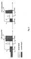
- Fig. 3shows such an AM signal and characteristics of the IF analog filters for two different IF frequencies, namely f IF1 as center frequency of a first analog filter which is obtained after a first downconversion from RF to IF1 and f IF2 as center frequency of a second analog filter which is obtained by a second downconversion from IF1 to IF2.
- the left hand side of Fig. 3shows the signal after the first downconversion. It is shown that the first IF analog filter has a passband of 20 kHz, i. e. the passband of the first IF analog filter has the range of f IF1 -10 kHz to f IF1 +10 kHz.
- unwanted signal parts 31a, 31bAdjacent to this wanted signal part 30 are unwanted signal parts 31a, 31b having smaller, equal or higher levels in comparison to the wanted signal part 30.
- a low frequency low level unwanted signal part 31a and a high frequency high level unwanted signal part 31bare shown.
- These unwanted signal parts 31a, 31blie within and outside the passband of the first IF analog filter.
- the bandwidth of the wanted signal part 30equal to 10 kHz, namely from f IF2 -5 kHz to f IF2 +5 kHz and a 20 kHz bandwidth of the second IF analog filter, namely from f IF2 -10 kHz to f IF2 +10 kHz.
- the unwanted signal parts 31a, 31blie adjacent to the wanted signal part 30 and have respective levels below, equal to and higher than the level of the wanted signal part 30.
- an adjacent disturbance signal eliminating circuitwhich eliminates an adjacent disturbance signal from an adjacent channel of a reception broadcast station by shifting the frequency of an intermediate frequency signal and shifting the frequency of an operating point of a PLL detection circuit simultaneously.
- a circuitis used for detecting an adjacent disturbance signal during fm detection by an adjacent disturbance signal detection circuit.
- the intermediate frequencyis shifted by a frequency difference and passes through a point shifted from the center frequency of a ceramic filter circuit by said frequency difference.
- the adjacent disturbance signalis shifted by said frequency difference and expelled toward a region having a large attenuation of the ceramic filter and the level of the adjacent disturbance signal is attenuated.
- JP 61 154325 Adiscloses a method for shifting a band frequency of an intermediate frequency. By tuning the frequencies of local oscillators, the intermediate frequency can be adjusted.
- the frequency of the first downconverter which shifts the center frequency of the wanted signal part from RF to the first IF frequency IF1is detuned in a way that a e.g. high level unwanted adjacent signal part lies outside the range of the first analog IF filter which is arranged behind said first downconverter.
- the first downconvertercuts-off an unwanted signal part adjacent to the wanted signal part and based on the obtained signal the following AGC stage automatically sets a correct amplification factor so that the desired resolution of wanted signal part can be obtained during the A/D conversion.
- the re-adjusting of the original center frequencycan be done in the digital baseband processing or during the second down conversion to the second IF frequency IF2.
- the best setting for such a "variable" first intermediate frequency 1F 1can be obtained by analyzing the power of the FFT carriers outside the wanted signal part or by BER (Bit Error Rate) fine tuning in the digital baseband processing or by optimizing the AGC control voltage.
- such a detuningcan also be performed during the second downconversion or during the first and the second downconversion. In the latter case it is also possible to cut-off unwanted signal parts on both sides of the wanted signal. In both cases the re-adjusting of the original center frequency has to be done in the digital baseband processing.
- Fig. 1shows a DRM-receiver according to the present invention.
- An AM signalis received by an antenna 1 and after amplification 2 the AM signal having a wanted signal part 30 with a center frequency fRF gets downconverted by a first downconverter 3 so that the center frequency of the wanted signal part equals to f IF1 , namely to the first intermediate frequency IF1.
- the received and downconverted AM signalgets further downconverted by a second downconverter 7 so that the center frequency f C2 of the wanted signal part equals to f IF2 , namely to the second intermediate frequency IF2.
- the resulting signalis filtered in a second IF analog filter 9 before amplification in an automatic gain control unit 10, A/D-conversion by an A/D-converter 11 and a following digital baseband processing 12.
- this processingis in conformity with that of a conventional DRM receiver.
- the first intermediate frequency f IF1is not fixed like in the receiver according to the prior art, but can be detuned from the possible frequency of 10,7 MHz so that a high frequency high level unwanted signal part 31b or a low frequency low level unwanted signal part 31a within the AM signal lies outside the filter range of the first IF analog filter 6. Therefore, according to the preferred embodiment of the present invention a PLL circuit 4 adjusts the output frequency of a first fixed oscillator 5 so that its output frequency f LO1 which is input to the first down-converter 3 determines the appropriate first intermediate frequency f IF1 based on a control signal which is supplied from the digital baseband processing stage 12.
- the detuning of the first intermediate frequencygets corrected during the digital baseband processing 12. Therefore, the downconversion to the second intermediate frequency, the second analog filtering, the automatic gain control and the A/D-conversion in-between the first intermediate frequency filering 6 and the digital baseband processing 12 is performed like in the DRM-receiver according to the prior art.
- the first IF analog filter 6cuts-off the high frequency high level unwanted signal part 31b and the low frequency unwanted signal part 31a basically has a level equal to the level of the wanted signal part 30, the energy of the wanted signal part 30 after the AGC 10 has an appropriate level and is not lowered or raised due to unwanted signal parts 31a, 31b with a level deviating from that of the wanted signal part 30.
- the first intermediate frequency f IF1can be detuned to either be higher or lower than the first intermediate frequency in a DRM-receiver according to the prior art so that a high or low level unwanted signal part 31a, 31b adjacent to the wanted signal part 30 lying on either one side of the wanted signal part 30 can be cut-off.
- the second intermediate frequency f IF2is also made variable by a second PLL circuit receiving the output frequency f LO2 of the second fixed oscillator 8 and supplying it to the second down-converter 7 it is also possible to cut-off unwanted signal parts on both sides of a wanted signal part, e.g. the low frequency unwanted signal part 31a can also be cut-off, in this case by the second IF analog filter 9.
- the second down-converter 7can also be used to set the predetermined second IF frequency f IF2 to the same frequency as used in the DRM-receiver according to the prior art. In this case no frequency correction has to be performed during the digital baseband processing 12.
- Fig. 2shows the downconverted AM signal in the first and second IF stages together with the filter characteristics of the first and second IF analog filters 6 and 9.
- the center frequency f C1 of the wanted signal part 30is not set to f IF1 which is the center frequency of the first IF analog filter 6, but offset by ⁇ f LO1 therefrom so that the high frequency high level unwanted signal part 31b is shifted to have a higher frequency to lie substantially outside the passband of the first IF analog filter 6. Since this high level high frequency unwanted signal part 31b is cut-off by the first IF analog filter 6 the automatic gain control 10 can shift the level of the wanted signal part 30 to an appropriate level for the following A/D-conversion 11.
- the second down-converter 7is triggered by the second fixed oscillator 8 directly no further frequency shift is introduced and the center frequency f C2 of the wanted signal part 30 in the second IF stage is offset from the center frequency f IF2 of the second IF analog filter 9 also by ⁇ f LO1 .
- the center frequency f C2 of the wanted signal part 30could be shifted to the appropriate second intermediate frequency f IF2 or further be offset to the low frequency side to cut-off the low frequency low level unwanted signal part 31a.
Landscapes
- Engineering & Computer Science (AREA)
- Computer Networks & Wireless Communication (AREA)
- Signal Processing (AREA)
- Superheterodyne Receivers (AREA)
- Circuits Of Receivers In General (AREA)
- Digital Transmission Methods That Use Modulated Carrier Waves (AREA)
Description
- The present invention relates to an AM receiver and a method of receiving and processing AM signals, in particular to such AM receivers which comprise an IF filter with a fixed IF bandwidth such as shortwave AM receivers with analog IF filters, in particular receivers for the Digital Radio Mondial (DRM) system.
- In the DRM system an IF bandwidth of 20 kHz is mandatory for receivers. Therefore, the analog IF filters within a receiver must have a 20 kHz bandwidth. On the other hand, a DRM signal and the existing analog signal which should also be processable in a DRM receiver might also have only a useful bandwidth of 10 kHz or even less, like in case of the existing analog AM signal.
- A problem raises if adjacent to such a wanted signal having a smaller bandwidth than the analog IF filters in a receiver an unwanted signal occurs, in particular if such a signal has a high level, since this signal which will not be suppressed by the analog IF filter leads to a wrong setting of the amplification factor of the following automatic gain control (AGC) circuit and therewith a desired resolution of the wanted signal part can not be obtained during an A/ D-conversion which is performed after the AGC and before the digital baseband processing.
- Fig. 3 shows such an AM signal and characteristics of the IF analog filters for two different IF frequencies, namely fIF1 as center frequency of a first analog filter which is obtained after a first downconversion from RF to IF1 and fIF2 as center frequency of a second analog filter which is obtained by a second downconversion from IF1 to IF2.
- The left hand side of Fig. 3 shows the signal after the first downconversion. It is shown that the first IF analog filter has a passband of 20 kHz, i. e. the passband of the first IF analog filter has the range of fIF1-10 kHz to fIF1+10 kHz. The AM signal which is downconverted to IF1 comprises a wanted
signal part 30 having a bandwidth of 10 kHz and a center frequency fC = fIF1, i. e. the frequeny range of the AM signal in the first IF stage is fIF1-5 kHZ to fIF1+5 kHz. Adjacent to this wantedsignal part 30 areunwanted signal parts signal part 30. In particular a low frequency low levelunwanted signal part 31a and a high frequency high levelunwanted signal part 31b are shown. Theseunwanted signal parts - The same is shown in the right hand side of Fig. 3 for the second IF stage with the center frequency fC of the wanted
signal part 30 equal to fIF2, the bandwidth of the wantedsignal part 30 equal to 10 kHz, namely from fIF2-5 kHz to fIF2+5 kHz and a 20 kHz bandwidth of the second IF analog filter, namely from fIF2-10 kHz to fIF2+10 kHz. Also in this case theunwanted signal parts signal part 30 and have respective levels below, equal to and higher than the level of the wantedsignal part 30. - In such a constellation that a high level
unwanted signal part 31b occurs adjacent to the small bandwidth wantedsignal part 30 the energy of the wanted signal after an automatic gain control stage arranged behind the second IF analog filter might be much lower than without theunwanted signal part 31b at the input of a following A/D-converter. - To cope with this problem, either the resolution or the sampling clock of the A/D-converter must be increased so that within the following digital baseband processing a desired resolution of the wanted signal part can be achieved which leads to a higher cost for the realization of the receiver.
- In
JP 02213228 A JP 61 154325 A - It is the object underlying the present invention to provide an improved AM receiver and method for receiving/processing an AM signal.
- This object is solved by an AM receiver according to independent claim 1 and a method to receive/process an AM signal according to independent claim 9. Respective preferred embodiments thereof are defined in the following dependent subclaims, respectively.
- According to a preferred embodiment of the present invention the frequency of the first downconverter which shifts the center frequency of the wanted signal part from RF to the first IF frequency IF1 is detuned in a way that a e.g. high level unwanted adjacent signal part lies outside the range of the first analog IF filter which is arranged behind said first downconverter.
- Therewith, according to the preferred embodiment of the present invention the first downconverter cuts-off an unwanted signal part adjacent to the wanted signal part and based on the obtained signal the following AGC stage automatically sets a correct amplification factor so that the desired resolution of wanted signal part can be obtained during the A/D conversion.
- The re-adjusting of the original center frequency can be done in the digital baseband processing or during the second down conversion to the second IF frequency IF2.
- The best setting for such a "variable" first intermediate frequency 1F 1 can be obtained by analyzing the power of the FFT carriers outside the wanted signal part or by BER (Bit Error Rate) fine tuning in the digital baseband processing or by optimizing the AGC control voltage.
- Of course, such a detuning can also be performed during the second downconversion or during the first and the second downconversion. In the latter case it is also possible to cut-off unwanted signal parts on both sides of the wanted signal. In both cases the re-adjusting of the original center frequency has to be done in the digital baseband processing.
- In the following the present invention is illucidated by an exemplary embodiment thereof with reference to the accompanying drawings, wherein
- Fig. 1
- shows a DRM-receiver according to the present invention;
- Fig. 2
- shows IF signals in the receiver shown in Fig. 1; and
- Fig. 3
- shows IF signals in a receiver according to the prior art.
- Fig. 1 shows a DRM-receiver according to the present invention. An AM signal is received by an antenna 1 and after amplification 2 the AM signal having a wanted
signal part 30 with a center frequency fRF gets downconverted by afirst downconverter 3 so that the center frequency of the wanted signal part equals to fIF1, namely to the first intermediate frequency IF1. After passing through a first IFanalog filter 6 the received and downconverted AM signal gets further downconverted by a second downconverter 7 so that the center frequency fC2 of the wanted signal part equals to fIF2, namely to the second intermediate frequency IF2. The resulting signal is filtered in a second IF analog filter 9 before amplification in an automaticgain control unit 10, A/D-conversion by an A/D-converter 11 and a following digital baseband processing 12. Basically, this processing is in conformity with that of a conventional DRM receiver. - However, according to the described preferred embodiment of the present invention the first intermediate frequency fIF1 is not fixed like in the receiver according to the prior art, but can be detuned from the possible frequency of 10,7 MHz so that a high frequency high level
unwanted signal part 31b or a low frequency low levelunwanted signal part 31a within the AM signal lies outside the filter range of the first IFanalog filter 6. Therefore, according to the preferred embodiment of the present invention a PLL circuit 4 adjusts the output frequency of a firstfixed oscillator 5 so that its output frequency fLO1 which is input to the first down-converter 3 determines the appropriate first intermediate frequency fIF1 based on a control signal which is supplied from the digital baseband processing stage 12. - The detuning of the first intermediate frequency gets corrected during the digital baseband processing 12. Therefore, the downconversion to the second intermediate frequency, the second analog filtering, the automatic gain control and the A/D-conversion in-between the first
intermediate frequency filering 6 and the digital baseband processing 12 is performed like in the DRM-receiver according to the prior art. Since according to the shown preferred embodiment of the present invention the first IFanalog filter 6 cuts-off the high frequency high levelunwanted signal part 31b and the low frequencyunwanted signal part 31a basically has a level equal to the level of the wantedsignal part 30, the energy of the wantedsignal part 30 after theAGC 10 has an appropriate level and is not lowered or raised due tounwanted signal parts signal part 30. - As is apparent from the foregoing description, the first intermediate frequency fIF1 can be detuned to either be higher or lower than the first intermediate frequency in a DRM-receiver according to the prior art so that a high or low level
unwanted signal part signal part 30 lying on either one side of the wantedsignal part 30 can be cut-off. - However, if the second intermediate frequency fIF2 is also made variable by a second PLL circuit receiving the output frequency fLO2 of the second fixed oscillator 8 and supplying it to the second down-converter 7 it is also possible to cut-off unwanted signal parts on both sides of a wanted signal part, e.g. the low frequency
unwanted signal part 31a can also be cut-off, in this case by the second IF analog filter 9. - Alternatively, in this case, the second down-converter 7 can also be used to set the predetermined second IF frequency fIF2 to the same frequency as used in the DRM-receiver according to the prior art. In this case no frequency correction has to be performed during the digital baseband processing 12.
- Fig. 2 shows the downconverted AM signal in the first and second IF stages together with the filter characteristics of the first and second IF
analog filters 6 and 9. In comparison to Fig. 3 the center frequency fC1 of the wantedsignal part 30 is not set to fIF1 which is the center frequency of the first IFanalog filter 6, but offset by ΔfLO1 therefrom so that the high frequency high levelunwanted signal part 31b is shifted to have a higher frequency to lie substantially outside the passband of the first IFanalog filter 6. Since this high level high frequencyunwanted signal part 31b is cut-off by the first IFanalog filter 6 theautomatic gain control 10 can shift the level of the wantedsignal part 30 to an appropriate level for the following A/D-conversion 11. Further, since in this embodiment the second down-converter 7 is triggered by the second fixed oscillator 8 directly no further frequency shift is introduced and the center frequency fC2 of the wantedsignal part 30 in the second IF stage is offset from the center frequency fIF2 of the second IF analog filter 9 also by ΔfLO1. - As discussed above, since the high level high frequency
unwanted signal part 31b is substantially cut-off by the first IFanalog filter 6 the center frequency fC2 of the wantedsignal part 30 could be shifted to the appropriate second intermediate frequency fIF2 or further be offset to the low frequency side to cut-off the low frequency low levelunwanted signal part 31a.
Claims (8)
- AM receiver comprising- at least one IF filter with a fixed IF bandwidth.- at least one down conversion stage (3,4,5) to shift the signal input thereto into an IF range (IFI), said at least one down conversion stage (3, 4, 5) having a variable oscillation frequency (flo1) which is adjustable to detune a wanted center frequency (fc) of a wanted signal part (30) from a center frequency (fIf1) of said at least one IF filter so that an unwanted signal part (31b) adjacent to said wanted signal part (30) lies outside said fixed IF bandwidth, andcharacterized in that it further comprises- a digital baseband processing stage, configured to readjust the detuned IF signal to a predetermined center frequency.
- AM receiver according to claim 1.characterized in that said means for readjusting is a further down conversion stage.
- AM receiver according to anyone of the preceding claims,characterized in that it is a digital shortwave receiver, in particular a Digital Radio Mondial receiver.
- AM receiver according to anyone of the preceding claims,characterized in that said least one IF filter is an analogue filter.
- AM receiver according to anyone of the preceding claims,characterized in that said fixed IF bandwidth is 20 kHz.
- AM receiver according to anyone of the preceding claims,characterized in that said unwanted signal part (31b) is detected by analyzing the power of FFT carriers outside the wanted signal part (30), BER fine tuning in a digital baseband processing or during optimization of an Automatic Gain Control voltage.
- Method to process a received AM signal wherein the received and eventually preprocessed AM signal gets shifted at least once into an IF range (IF1), comprising the steps of:- detuning a wanted center frequency (fc) of a wanted signal part (30) from a center frequency (fill) used during at least one IF filtering with a fixed IF bandwidth so that an unwanted signal part (31b) adjacent to said wanted signal part (30) lies outside said fixed IF bandwidth, andcharacterized in the step of- readjusting the detuned IF signal to a predetermined center frequency in a digital baseband processing stage.
- Method according to claim 9,characterized in that it is used for digital shortwave reception, in particular Digital Radio Mondial reception.
Priority Applications (4)
| Application Number | Priority Date | Filing Date | Title |
|---|---|---|---|
| EP00110526AEP1156589B1 (en) | 2000-05-17 | 2000-05-17 | AM receiver |
| DE60037722TDE60037722T2 (en) | 2000-05-17 | 2000-05-17 | AM receiver |
| US09/855,422US7155189B2 (en) | 2000-05-17 | 2001-05-15 | AM receiver |
| JP2001148291AJP2002026759A (en) | 2000-05-17 | 2001-05-17 | Receiver of amplitude modulation system |
Applications Claiming Priority (1)
| Application Number | Priority Date | Filing Date | Title |
|---|---|---|---|
| EP00110526AEP1156589B1 (en) | 2000-05-17 | 2000-05-17 | AM receiver |
Publications (2)
| Publication Number | Publication Date |
|---|---|
| EP1156589A1 EP1156589A1 (en) | 2001-11-21 |
| EP1156589B1true EP1156589B1 (en) | 2008-01-09 |
Family
ID=8168755
Family Applications (1)
| Application Number | Title | Priority Date | Filing Date |
|---|---|---|---|
| EP00110526AExpired - LifetimeEP1156589B1 (en) | 2000-05-17 | 2000-05-17 | AM receiver |
Country Status (4)
| Country | Link |
|---|---|
| US (1) | US7155189B2 (en) |
| EP (1) | EP1156589B1 (en) |
| JP (1) | JP2002026759A (en) |
| DE (1) | DE60037722T2 (en) |
Families Citing this family (9)
| Publication number | Priority date | Publication date | Assignee | Title |
|---|---|---|---|---|
| EP1073224A3 (en)* | 1999-05-07 | 2002-08-14 | Sony International (Europe) GmbH | Strategy for switching to Alternative Frequencies (AF) for Digital Radio Mondiale (DRM) |
| DE60129342T2 (en) | 2001-12-05 | 2008-03-20 | Sony Deutschland Gmbh | FM receiver with digital bandwidth control |
| US7221917B2 (en)* | 2002-05-01 | 2007-05-22 | Ibiquity Digital Corporation | Adjacent channel interference mitigation for FM digital audio broadcasting receivers |
| US7127008B2 (en) | 2003-02-24 | 2006-10-24 | Ibiquity Digital Corporation | Coherent AM demodulator using a weighted LSB/USB sum for interference mitigation |
| JP2007509559A (en) | 2003-10-21 | 2007-04-12 | コーニンクレッカ フィリップス エレクトロニクス エヌ ヴィ | Analog-to-digital conversion and suppression system |
| US7787829B1 (en)* | 2003-12-23 | 2010-08-31 | Cypress Semiconductor Corporation | Method and apparatus for tuning a radio receiver with a radio transmitter |
| US7746922B2 (en)* | 2005-12-07 | 2010-06-29 | Cypress Semiconductor Corporation | Apparatus and method for frequency calibration between two radios |
| ATE470270T1 (en)* | 2008-03-26 | 2010-06-15 | Ericsson Telefon Ab L M | METHOD FOR PROCESSING A BASEBAND SIGNAL |
| WO2016183720A1 (en)* | 2015-05-15 | 2016-11-24 | 华为技术有限公司 | Downlink and uplink compression method and device using non-standard bandwidth of lte system |
Citations (2)
| Publication number | Priority date | Publication date | Assignee | Title |
|---|---|---|---|---|
| JPS61154325A (en)* | 1984-12-27 | 1986-07-14 | Yaesu Musen Co Ltd | Band frequency shifting method |
| JPH01232832A (en)* | 1988-03-14 | 1989-09-18 | Fujitsu Ten Ltd | Receiver |
Family Cites Families (45)
| Publication number | Priority date | Publication date | Assignee | Title |
|---|---|---|---|---|
| GB797705A (en)* | 1956-01-20 | 1958-07-09 | Marconi Wireless Telegraph Co | Improvements in or relating to narrow band selective circuit arrangements |
| US3204185A (en)* | 1961-04-19 | 1965-08-31 | North American Aviation Inc | Phase-lock receivers |
| US3946148A (en)* | 1974-10-03 | 1976-03-23 | Zenith Radio Corporation | Television receiver operable in exact or extended range tuning modes |
| JPS5826699B2 (en)* | 1975-11-13 | 1983-06-04 | ソニー株式会社 | Chuyuna |
| DE2612720C2 (en)* | 1976-03-25 | 1977-09-29 | Siemens AG, 1000 Berlin und 8000 München | Tunable, selective heterodyne receiver |
| JPS53116017A (en)* | 1977-03-19 | 1978-10-11 | Sony Corp | Automatic frequency control system for ssb receivers |
| AU4953979A (en)* | 1978-08-16 | 1980-02-21 | Sony Corporation | Receiver tuning with frequency synthesizer |
| US4288875A (en)* | 1980-02-08 | 1981-09-08 | Rca Corporation | Controlled local oscillator with apparatus for extending its frequency range |
| FR2526609A1 (en)* | 1982-05-04 | 1983-11-10 | Thomson Csf | MULTI-PORT SIGNAL RECEIVER PROTECTS DISTURBING SIGNALS |
| US4479257A (en)* | 1982-12-30 | 1984-10-23 | Yaesu Musen Co., Ltd. | Superheterodyne circuit having variable bandwidth and center frequency shift function |
| US4715001A (en)* | 1984-08-23 | 1987-12-22 | Motorola, Inc. | Extremely accurate automatic frequency control circuit and method therefor |
| US4619000A (en)* | 1984-09-24 | 1986-10-21 | John Ma | CATV converter having improved tuning circuits |
| FR2596220A1 (en)* | 1986-03-21 | 1987-09-25 | Portenseigne | FREQUENCY DEMODULATOR |
| JPH02213228A (en)* | 1989-02-14 | 1990-08-24 | Kenwood Corp | Adjacent disturbance signal eliminating circuit |
| US5802462A (en)* | 1990-05-24 | 1998-09-01 | Emhiser Research Limited | FM-PM receivers with frequency deviation compression |
| DE4127501A1 (en)* | 1990-09-07 | 1992-03-12 | Telefunken Systemtechnik | METHOD FOR DETECTING THE FREQUENCY STORAGE IN DIGITAL MESSAGE TRANSMISSIONS |
| US5097221A (en)* | 1990-12-21 | 1992-03-17 | The United States Of America As Represented By The Secretary Of The Navy | Adaptive filter technique for suppression of wideband or offset narrowband radio frequency interference |
| US5146227A (en)* | 1991-05-03 | 1992-09-08 | Whistler Corporation | Sweeping receiver |
| JP2912791B2 (en)* | 1993-06-01 | 1999-06-28 | 松下電器産業株式会社 | High frequency receiver |
| FI109736B (en)* | 1993-11-01 | 2002-09-30 | Nokia Corp | Changing the receiver's frequency range and bandwidth using a mirror-frequency-damping mixer |
| US5970400A (en)* | 1996-04-30 | 1999-10-19 | Magellan Corporation | Adjusting the timing and synchronization of a radio's oscillator with a signal from an SATPS satellite |
| FI102229B1 (en)* | 1996-11-05 | 1998-10-30 | Nokia Mobile Phones Ltd | Method to improve tuning of the radio receiver and a radio receiver |
| US5852772A (en)* | 1997-02-25 | 1998-12-22 | Ericsson Inc. | Receiver IF system with active filters |
| GB2326038A (en)* | 1997-06-06 | 1998-12-09 | Nokia Mobile Phones Ltd | Signal level balancing in quadrature receiver |
| US6178314B1 (en)* | 1997-06-27 | 2001-01-23 | Visteon Global Technologies, Inc. | Radio receiver with adaptive bandwidth controls at intermediate frequency and audio frequency sections |
| US6308048B1 (en)* | 1997-11-19 | 2001-10-23 | Ericsson Inc. | Simplified reference frequency distribution in a mobile phone |
| JPH11177646A (en)* | 1997-12-12 | 1999-07-02 | Matsushita Electric Ind Co Ltd | Demodulator |
| SE521035C2 (en)* | 1997-12-29 | 2003-09-23 | Ericsson Telefon Ab L M | A receiver and a method for mobile radio, where the receiver is adapted for different radio communication networks, eg GSM, AMPS |
| US6161004A (en)* | 1998-03-02 | 2000-12-12 | Mentor Graphics Corporation | Method and apparatus for rejecting image signals in a receiver |
| GB2336731A (en)* | 1998-04-22 | 1999-10-27 | Thomson Multimedia Sa | A video tuner in which data representing a PLL division is used to control other circuit parameters |
| US6088569A (en)* | 1998-04-23 | 2000-07-11 | Motorola, Inc. | Method and apparatus for receiving a plurality of signals having different frequency bandwidths |
| JP3912459B2 (en)* | 1998-06-16 | 2007-05-09 | ソニー株式会社 | Receiving machine |
| US6061551A (en)* | 1998-10-21 | 2000-05-09 | Parkervision, Inc. | Method and system for down-converting electromagnetic signals |
| US6256301B1 (en)* | 1998-10-15 | 2001-07-03 | Qualcomm Incorporated | Reservation multiple access |
| US6591091B1 (en)* | 1998-11-12 | 2003-07-08 | Broadcom Corporation | System and method for coarse/fine PLL adjustment |
| US6895232B2 (en)* | 1999-05-07 | 2005-05-17 | Conexant Systems, Inc. | Method and apparatus for receiving radio frequency signals |
| US6683919B1 (en)* | 1999-06-16 | 2004-01-27 | National Semiconductor Corporation | Method and apparatus for noise bandwidth reduction in wireless communication signal reception |
| US6326790B1 (en)* | 1999-08-04 | 2001-12-04 | Ellen Ott | Ground piercing metal detector having range, bearing and metal-type discrimination |
| KR100314113B1 (en)* | 1999-08-25 | 2001-11-15 | 구자홍 | matched filter and filtering method, apparatus and method for receiving plural digital broadcast using digital filter |
| US6658245B2 (en)* | 2001-03-28 | 2003-12-02 | Motorola, Inc. | Radio receiver having a dynamic bandwidth filter and method therefor |
| US6785527B2 (en)* | 2001-04-02 | 2004-08-31 | Tektronix, Inc. | Conversion spur avoidance in a multi-conversion radio frequency receiver |
| US7386286B2 (en)* | 2001-06-01 | 2008-06-10 | Broadband Innovations, Inc. | High frequency low noise phase-frequency detector and phase noise reduction method and apparatus |
| US6957054B2 (en)* | 2002-08-09 | 2005-10-18 | Freescale Semiconductor, Inc. | Radio receiver having a variable bandwidth IF filter and method therefor |
| US7088189B2 (en)* | 2003-09-09 | 2006-08-08 | Synergy Microwave Corporation | Integrated low noise microwave wideband push-push VCO |
| US7005927B2 (en)* | 2004-05-28 | 2006-02-28 | Tektronix, Inc. | Low noise YIG oscillator based phase locked loop |
- 2000
- 2000-05-17EPEP00110526Apatent/EP1156589B1/ennot_activeExpired - Lifetime
- 2000-05-17DEDE60037722Tpatent/DE60037722T2/ennot_activeExpired - Lifetime
- 2001
- 2001-05-15USUS09/855,422patent/US7155189B2/ennot_activeExpired - Fee Related
- 2001-05-17JPJP2001148291Apatent/JP2002026759A/ennot_activeWithdrawn
Patent Citations (2)
| Publication number | Priority date | Publication date | Assignee | Title |
|---|---|---|---|---|
| JPS61154325A (en)* | 1984-12-27 | 1986-07-14 | Yaesu Musen Co Ltd | Band frequency shifting method |
| JPH01232832A (en)* | 1988-03-14 | 1989-09-18 | Fujitsu Ten Ltd | Receiver |
Also Published As
| Publication number | Publication date |
|---|---|
| DE60037722T2 (en) | 2009-01-15 |
| DE60037722D1 (en) | 2008-02-21 |
| EP1156589A1 (en) | 2001-11-21 |
| JP2002026759A (en) | 2002-01-25 |
| US20010044288A1 (en) | 2001-11-22 |
| US7155189B2 (en) | 2006-12-26 |
Similar Documents
| Publication | Publication Date | Title |
|---|---|---|
| US6118499A (en) | Digital television signal receiver | |
| EP2034614B1 (en) | FM tuner | |
| WO1993003550A1 (en) | Intermodulation controller for radio receiver | |
| US8213892B2 (en) | FM-AM demodulator and control method therefor | |
| EP1156589B1 (en) | AM receiver | |
| US7269401B2 (en) | Signal processing circuit for tuner which applies signal processing based on variation in frequency of intermediate frequency signal | |
| US7123892B2 (en) | Architecture for an AM/FM digital intermediate frequency radio | |
| US20080152049A1 (en) | Digital audio broadcast receiver | |
| KR100560192B1 (en) | Digital Broadcast Receiver | |
| KR100233658B1 (en) | Method for reducing time to recover carrier wave in hdtv | |
| JP4235560B2 (en) | Automatic gain control for tuners | |
| EP1383248B1 (en) | Superheterodyne receiver | |
| JP4089275B2 (en) | Reception control method, reception control device, and reception device | |
| JP4506426B2 (en) | COFDM modulation receiver and adjacent channel interference elimination method | |
| EP0944213B1 (en) | Digital broadcast receiver | |
| JP3324465B2 (en) | Digital audio broadcast receiver | |
| JP6887890B2 (en) | Semiconductor devices and their methods | |
| KR100282944B1 (en) | Carrier wave a fine recovery apparatus and method | |
| JPH06291688A (en) | Receiver | |
| KR0162437B1 (en) | Frequency automatic fine tuning device and method of digital satellite broadcasting receiver | |
| JPH0254705B2 (en) | ||
| EP1380108A2 (en) | Methods and apparatus for tuning pre-selection filters in radio receivers | |
| EP2764628B1 (en) | Signal reception multi-tuner system and corresponding method | |
| KR0173229B1 (en) | Digital satellite tuner | |
| WO2003096535A1 (en) | Method and radio frequency receiver apparatus for processes radio frequency signals |
Legal Events
| Date | Code | Title | Description |
|---|---|---|---|
| PUAI | Public reference made under article 153(3) epc to a published international application that has entered the european phase | Free format text:ORIGINAL CODE: 0009012 | |
| AK | Designated contracting states | Kind code of ref document:A1 Designated state(s):AT BE CH CY DE DK ES FI FR GB GR IE IT LI LU MC NL PT SE Kind code of ref document:A1 Designated state(s):DE FR GB | |
| AX | Request for extension of the european patent | Free format text:AL;LT;LV;MK;RO;SI | |
| 17P | Request for examination filed | Effective date:20011213 | |
| AKX | Designation fees paid | Free format text:DE FR GB | |
| RAP1 | Party data changed (applicant data changed or rights of an application transferred) | Owner name:SONY DEUTSCHLAND GMBH | |
| 17Q | First examination report despatched | Effective date:20060508 | |
| RAP1 | Party data changed (applicant data changed or rights of an application transferred) | Owner name:SONY DEUTSCHLAND GMBH | |
| GRAP | Despatch of communication of intention to grant a patent | Free format text:ORIGINAL CODE: EPIDOSNIGR1 | |
| GRAS | Grant fee paid | Free format text:ORIGINAL CODE: EPIDOSNIGR3 | |
| GRAA | (expected) grant | Free format text:ORIGINAL CODE: 0009210 | |
| AK | Designated contracting states | Kind code of ref document:B1 Designated state(s):DE FR GB | |
| REG | Reference to a national code | Ref country code:GB Ref legal event code:FG4D | |
| REF | Corresponds to: | Ref document number:60037722 Country of ref document:DE Date of ref document:20080221 Kind code of ref document:P | |
| ET | Fr: translation filed | ||
| PLBE | No opposition filed within time limit | Free format text:ORIGINAL CODE: 0009261 | |
| STAA | Information on the status of an ep patent application or granted ep patent | Free format text:STATUS: NO OPPOSITION FILED WITHIN TIME LIMIT | |
| 26N | No opposition filed | Effective date:20081010 | |
| PGFP | Annual fee paid to national office [announced via postgrant information from national office to epo] | Ref country code:GB Payment date:20140521 Year of fee payment:15 | |
| PGFP | Annual fee paid to national office [announced via postgrant information from national office to epo] | Ref country code:FR Payment date:20140527 Year of fee payment:15 Ref country code:DE Payment date:20140521 Year of fee payment:15 | |
| REG | Reference to a national code | Ref country code:DE Ref legal event code:R119 Ref document number:60037722 Country of ref document:DE | |
| GBPC | Gb: european patent ceased through non-payment of renewal fee | Effective date:20150517 | |
| REG | Reference to a national code | Ref country code:FR Ref legal event code:ST Effective date:20160129 | |
| PG25 | Lapsed in a contracting state [announced via postgrant information from national office to epo] | Ref country code:DE Free format text:LAPSE BECAUSE OF NON-PAYMENT OF DUE FEES Effective date:20151201 Ref country code:GB Free format text:LAPSE BECAUSE OF NON-PAYMENT OF DUE FEES Effective date:20150517 | |
| PG25 | Lapsed in a contracting state [announced via postgrant information from national office to epo] | Ref country code:FR Free format text:LAPSE BECAUSE OF NON-PAYMENT OF DUE FEES Effective date:20150601 |