EP1156321B1 - Method for checking a surface to be analysed and scanning surface-analyser - Google Patents
Method for checking a surface to be analysed and scanning surface-analyserDownload PDFInfo
- Publication number
- EP1156321B1 EP1156321B1EP99973123AEP99973123AEP1156321B1EP 1156321 B1EP1156321 B1EP 1156321B1EP 99973123 AEP99973123 AEP 99973123AEP 99973123 AEP99973123 AEP 99973123AEP 1156321 B1EP1156321 B1EP 1156321B1
- Authority
- EP
- European Patent Office
- Prior art keywords
- light
- revolution
- mirror
- analysed
- analysed surface
- Prior art date
- Legal status (The legal status is an assumption and is not a legal conclusion. Google has not performed a legal analysis and makes no representation as to the accuracy of the status listed.)
- Expired - Lifetime
Links
- 238000000034methodMethods0.000titleclaimsdescription27
- 230000007547defectEffects0.000claimsdescription14
- 238000012544monitoring processMethods0.000claimsdescription12
- 241000252254CatostomidaeSpecies0.000claimsdescription6
- 238000012937correctionMethods0.000claimsdescription6
- 239000006096absorbing agentSubstances0.000claimsdescription4
- 239000004065semiconductorSubstances0.000description14
- 235000012431wafersNutrition0.000description14
- 238000010586diagramMethods0.000description8
- 238000004519manufacturing processMethods0.000description6
- 239000002245particleSubstances0.000description6
- 238000012545processingMethods0.000description5
- 238000005516engineering processMethods0.000description4
- 238000005259measurementMethods0.000description3
- 230000003287optical effectEffects0.000description3
- 238000000149argon plasma sinteringMethods0.000description2
- 239000000428dustSubstances0.000description2
- 238000004458analytical methodMethods0.000description1
- 230000003749cleanlinessEffects0.000description1
- 238000007689inspectionMethods0.000description1
- 230000000750progressive effectEffects0.000description1
- 239000007787solidSubstances0.000description1
Images


Classifications
- G—PHYSICS
- G01—MEASURING; TESTING
- G01N—INVESTIGATING OR ANALYSING MATERIALS BY DETERMINING THEIR CHEMICAL OR PHYSICAL PROPERTIES
- G01N21/00—Investigating or analysing materials by the use of optical means, i.e. using sub-millimetre waves, infrared, visible or ultraviolet light
- G01N21/84—Systems specially adapted for particular applications
- G01N21/88—Investigating the presence of flaws or contamination
- G01N21/95—Investigating the presence of flaws or contamination characterised by the material or shape of the object to be examined
- G01N21/9501—Semiconductor wafers
Definitions
- the present inventionrelates to the optical instrument engineering and can be used particularly in developing new and improving existing devices for investigating a surface of semiconductor wafers and building devices into the technology equipment, as well as for investigating a uniformity degree of a surface of other articles.
- a method for monitoring an analysed surfaceis known from the US Patent 1 4314763 (Int.Cl. G 01 N 21/88, 09.02.82), comprising steps of: performing a rotation of the analysed surface about a centre of revolution, forming a light spot on the analysed surface, and sensing a light scattered by the analysed surface using an optical system.
- a surface scanning analysercomprising a light source intended for illuminating an analysed surface by a light spot at an angle close to the normal to this analysed surface, a photodetector intended for sensing the light scattered by the analysed surface, and a rotating table for mounting an article with the analysed surface on it and rotating it about an axis of revolution parallel to the normal to the analysed surface.
- the closest analogue to the claimed inventionis a method for monitoring the analysed surface comprised steps of: performing a rotation of an object having the analysed surface about a first centre of revolution; forming a light spot on the analysed surface; sensing separately a light mirror-reflected and scattered by the analysed surface in the incidence point of the light spot (Altendorfer H. et al. "Unpattemed surface inspection for next-generation devices”. - Solid State Technology, 1996, v. 39, 1 8, pp. 93-97).
- a surface scanning analysercomprising: a rotating table for mounting on it an object with an analysed surface and for rotating it about its first axis of revolution that is perpendicular to the analysed surface; a light source intended for illuminating the analysed surface by a light spot at an angle close to the normal to the analysed surface; a gathering mirror in the form of a truncated body of revolution formed by revolving an ellipse about a second axis of revolution which is parallel to the first axis of revolution and substantially coincides with the normal to the analysed surface erected in its incidence point of said light spot, said incidence point being in the focus of said truncated body of revolution, which first section plane is located perpendicularly to the second axis of revolution in the immediate proximity to said focus, and a second section plane of the body of revolution is parallel to its first section plane; a photodetector intended for sensing the light scattered from the analysed surface and reflected by the gathering mirror.
- the object of this inventionis to develop such methods for monitoring the analysed surface and a surface scanning analyser that would be free from the indicated drawbacks.
- the inventionrelates to a method for monitoring an analysed surface comprised steps of: performing a rotation of an object having the analysed surface about a first centre of revolution; forming a light spot on the analysed surface; sensing separately a light mirror-reflected and scattered by the analysed surface in the incidence point of the light spot.
- the methodincludes steps of: performing a movement of the light spot relative to the analysed surface along an arc about a second centre of revolution, which lies off the analysed surface; aligning, at least in one predetermined position, the light spot having an elongated form on the analysed surface with its maximum size along a radius from the first centre of revolution tgrough the centre of the light spot.
- a feature of this methodis that in the predetermined position the light spot is located substantially in the middle of said analysed surface radius from the first centre of revolution, or the light spot, during its movement along said arc, is turned aside so as to retain its alignment along the radius from the first centre of revolution thought the centre of the light spot all the scanning line.
- the light scattered by the analysed surfaceis gathered using a system of mirrors, one of which is made in the form of a truncated ellipsoid of revolution, which one axis of revolution substantially coincides with the normal to the analysed surface erected in its incidence point of said light spot, said incidence point being in a first focus of said truncated ellipsoid of revolution which first section plane is located perpendicularly to its axis of revolution in the immediate proximity to said first focus, a second section plane of the ellipsoid of revolution being parallel to its first section plane, and another mirror is a flat mirror having an aperture in its centre, arranged at an angle to the axis of revolution of the truncated ellipsoid of revolution, and intended for passing through it the light from the light source to the analysed surface and the light mirror-reflected from it and for reflecting the light scattered by the analysed surface and reflected by the gathering mirror, wherein the light reflected by the
- the feature of this methodis that the light scattered by the analysed surface is gathered using a system of mirrors, one of which is made in the form of a truncated paraboloid of revolution, which axis of revolution substantially coincides with the normal to the analysed surface erected in its incidence point of said light spot, said incidence point being in a focus of said truncated paraboloid of revolution which first section plane is located perpendicularly to its axis of revolution in the immediate proximity to said focus, a second section plane of the paraboloid of revolution being parallel to its first section plane, and another mirror is a flat mirror having an aperture in its centre, arranged at an angle to the axis of revolution of the truncated paraboloid of revolution, and intended for passing through it the light from the light source to the analysed surface and the light mirror-reflected from it and for reflecting the light scattered by the analysed surface and reflected by the gathering mirror, wherein the light reflected by the flat mirror is passed through a light filter, gathered using a
- the present inventionrelates to a surface scanning analyser comprising: a rotating table for mounting on it an object with an analysed surface and for rotating it about its first axis of revolution that is perpendicular to the analysed surface; a light source intended for illuminating the analysed surface by a light spot at an angle close to the normal to the analysed surface; a gathering mirror in the form of a truncated body of revolution formed by revolving a second order curve about a second axis of revolution which is parallel to the first axis of revolution and substantially coincides with the normal to the analysed surface erected in its incidence point of said light spot, said incidence point being in the focus of said truncated body of revolution, which first section planc is located perpendicularly to the second axis of revolution in the immediate proximity to said focus, and a second section plane of the body of revolution is parallel to its first section plane; a first light sensing unit intended for sensing the light mirror-reflected from the analysed surface and located close to the
- the first light sensing unitis a light absorber or a photodetector to determine the presence of non-scattering defects on the analysed surface.
- the second light sensing unitis intended for sensing the light reflected from the flat mirror.
- the body of revolution of the gathering mirroris an ellipsoid of revolution in which second focus with regard of reflecting from the flat mirror a diaphragm is mounted intended for passing through it the light reflected from the flat mirror to the second light sensing unit.
- a light filtercan be mounted between the flat mirror and the diaphragm.
- a feature in another variantis that the body of revolution of the gathering mirror is a paraboloid of revolution, and a gathering lens and diaphragm are mounted between the flat mirror and the second light sensing unit, intended for gathering and passing through them the light reflected from the flat mirror to the second light sensing unit.
- a light filtercan mounted between the flat mirror and the gathering lens.
- This analyserfurther comprises a drive for rotating the housing to enable a possibility for moving the housing over the analysed surface at least to one side from its centre of revolution.
- Yet one more feature of this analyseris that in said predetermined position of the housing, said light spot is located substantially in the middle of said analysed surface radius from the centre of its revolving, or in that the drive for rotating the housing is provided with means for measuring a rotating angle of the housing, and the light source is provided with means for correcting a position, which is intended for turning aside the light source in accordance with signals from means for measuring the rotating angle intended for enabling said aligning of the light spot along the radius from the centre of revolution of the analysed surface all the scanning line.
- the housingis made light-absorbing from the inside.
- the rotating tableis provided with three vacuum suckers located symmetrically about the first axis of revolution and intended for mounting the object with the analysed surface on the rotating table.
- a line movement of the assembly with the light source and light sensing unit along the rotating analysed surfaceis known from the Japan Unexamined Application 1 03-163338 (Int.Cl. G 01 N 21/88, 15.07.91).
- a usage of the rotating housing in the form of the tone armis known as such from disk turntables.
- a usage of the gathering mirror in the form of the ellipsoid of revolutionis also known.
- USSR Author's Certificate 1 1297590(Int.Cl. G 01 N 21/47, 15.11.86) a usage of the gathering mirror in the form of the paraboloid of revolution is also known.
- the method for monitoring the analysed surface according to the present inventioncan be realised using the scanning analyser made in accordance with the present invention, which example is shown in the attached drawings.
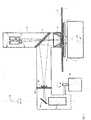
- Fig. 1shows the structure diagram of the optical-mechanical part of the surface scanning analyser in accordance with the present invention.
- An object 1 with an analysed surface 2is mounted on the rotating table 3 which is provided with vacuum suckers 4.
- the vacuum suckersare located symmetrically about the centre of revolution of the rotating table 3, i.e. spaced at 120° along the arc about its centre of revolution.
- the rotating table 3has a revolving motor 5 (particularly, the stepper) for permitting the revolution of the rotating table about the first axis 6 of revolution.
- the present inventionutilises the known fact that defects on the smooth surface scatter the incident light sideways while illuminating said surface with a light beam in the direction close to the normal to this surface.
- the analysed surface 2is illuminated with a light source 7 which comprises a semiconductor laser.
- the light from the source 7is gathered and focused with a lens 8 into a spot on the analysed surface 2.
- the light source 7 with the lens 8is disposed over the object 1 when it is mounted on the rotating table 3, so that the light beam onto the analysed surface 2 has a direction close to the normal to this surface.
- the normal to the analysed surface 2 in its incident point of the light beam from the light source 7coincides with the first axis of revolution 6, this is done only to make an understanding of the present invention more easy.
- a first light sensing unit 9is disposed, which is intended for sensing the light mirrored from the analysed surface 2.
- the first light sensing unit 9can be merely an absorber which prevents for reflecting the light mirror-reflected from the analysed surface 2 back to it.
- this unit as a photodetector 9can sense the light mirror-reflected from the analysed surface 2 in order to determine the presence of non-scattering defects of different types on the surface of the monitored object 1 (for example, a semiconductor wafer) from a change of the intensity of the light mirror-reflected from the analysed surface 2.
- a gathering mirror 10is employed made in the form of a body of revolution formed by revolving a second order curve about a second axis of revolution which is parallel to the first axis of revolution and substantially coincides with the normal to the analysed surface erected in its incidence point of said light spot.
- the second axis of revolutioncoincides with the first axis of revolution 6, but this is done only to make an understanding of the present invention more easy.
- an ellipse or parabolais selected, one focus of the ellipse or the focus of the parabola coinciding with the incident point of the light from the source 7 onto the analysed surface 2.
- the body of revolutionis made truncated, its first section plane being located perpendicularly to the second axis of revolution in the immediate proximity to said focus, and a second section plane of the body of revolution being parallel to its first section plane.
- a so formed gap between the edge of the gathering mirror 10 located in the first section plane, and the analysed surface 2enables a free movement of the gathering mirror 10 over the analysed surface 2.
- the light scattered by defects of the analysed surfacefalls onto the inner reflecting surface of the gathering mirror 10 and is reflected aside from the analysed surface 2 either parallel to its normal in the case of parabolic shape of the mirror 10, or to the point of another focus in the case of elliptical shape of the gathering mirror 10.
- a flat mirror 11 with an aperture in its centreis used, which is mounted at an angle to the normal to the analysed surface 2 (to the second axis of revolution about which the above mentioned second order curve, parabola or ellipse, is revolved).
- This angle in Fig. 1is 45°, but it may have another value if necessary.
- the aperture in the centre of the flat mirror 11enables an unimpeded passing of the light from the light source 7 to the analysed surface 2 and the reflection from it to the first light sensing unit 9.
- the flat mirror 11reflects the light gathered and reflected by the gathering mirror 10 aside from the direction of propagation of the light from the source 7.
- the lightBefore the gathering lens 12 the light may be passed through a light filter 15 for choosing the light only with a required wavelength and optionally is the direction of the light is changed by means of an additional mirror 16 when the second light sensing unit 14 is mounted not in the direction onto the flat mirror 11.
- a light filter 15for choosing the light only with a required wavelength and optionally is the direction of the light is changed by means of an additional mirror 16 when the second light sensing unit 14 is mounted not in the direction onto the flat mirror 11.
- the gathering mirror 10when the gathering mirror 10 is made in the form of ellipsoid of revolution, the light reflected by it will be gathered in the second focus of this ellipsoid. After reflecting from the flat mirror 11 this second focus will be as if turned and found on one side of the second axis of revolution (the propagation line of the light from the source 7).
- the diaphragm 13is mounted just in the point of the second focus of the ellipsoid of revolution with regard to its displacing due to the reflection from the flat mirror 11.
- the light filter 15 and additional mirror 16can be used like in the case of making the gathering mirror 10 in the form of paraboloid of revolution.
- the light source 7, lens 8 gathering mirror 10, flat mirror 11, first and second light sensing units 9, 14, as well as light path elements indicated by numbers 12, 13, 15 and 16are placed into the housing 17 which can be made light-absorbing from the inside.
- the housing 17is provided with a drive (not shown) having a rotating motor 18 (particularly, the stepper) which enables a rotation of the housing 17 about a third axis of revolution 19 parallel to the first axis of revolution 6 and passing off the object 1 with the analysed surface 2 and/or the rotating table 3.
- the rotating drive 18enables movements of the housing 17 so that the a light spot 21 formed by the light source 7 on the analysed surface 2 is moved along an arc 22 passing via the centre 23 of the analysed surface 2 at least to one side from the centre 23 of revolution up to the edge of the analysed surface 2.
- the light spot 21 formed on the analysed surface 2 and having an elongated shapewill trace the arc 22 about the second centre 24 of revolution (being a projection of the third axis of revolution 19 onto the plane of Fig. 3).
- the light spot 21will be directed at some angle to the radius 25 from the first centre 23 of revolution (being a projection of the first axis of revolution 19 onto the plane of Fig. 3) of the analysed surface 2, which passes via this point.
- the optimum orientation of the light spotis in aligning its maximum size (the long axis of the spot) along the radius 25 passing via that point where the light spot 21 is formed at this moment.
- the light spot 21 having the elongated shape on the analysed surface 2is aligned, at least in one predetermined position, with its maximum size along a radius 25 from the first centre 23 of rotation through the centre of the spot.
- Such predetermined position where the radius 25 crosses the arc 22 (a scanning line)can be particularly the middle of the radius 25.
- the light source 7 and lens 8are mounted so as the light spot 21, when forming in the middle of distance from the centre 23 of revolution to the edge of the analysed surface 2, is aligned with its maximum size (the long axis) exactly along the radius 25 from the first centre of rotation 23 through the centre of the spot 21.
- the light source 7 and lens 8can be provided with means 20 for position correction. It may be, for instance, a micromotor (particularly, a stepper).
- the drive with the rotating motor 18is provided with means for measuring a rotating angle of the housing (not shown) relative to its initial position. Then signals from this means for measuring a rotating angle of the housing, after their corresponding processing, can be fed to the means 20 for position correction which will turn aside the light source 7 with the lens 8 so as to retain the alignment of the light spot 21 along the radius 25 from the first centre 23 of rotation via the light spot all the scanning line (the arc 22).
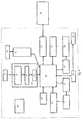
- a circuitcan be used shown in Fig. 4. This circuit is merely illustrative and serves only to confirm the practicability of the present invention.
- a signal processor 26is connected via a parallel interface 27 to a control computer 28 in which memory a program for operating the surface scanning analyser according to the present invention is stored. This program can be composed in accordance with a list of operations below.
- the parallel interfacecarries out the data exchange between the control computer 28 and signal processor 26 in accordance with requirements of the IEEE-1284 Standard, ensuring a compatibility with the majority of computers presently employed.
- the signal processor 26is connected with its inputs to a rotating table angle position transducer 29 and housing rotational angle transducer 30 which is in this case an example of embodiment for the above mentioned means for measuring a rotating angle of the housing.
- the transducers 29 and 30are coupled mechanically to a shaft of the revolving drive 5 and to a shaft of the rotating drive 18 respectively, the control of which drives is performed on signals from corresponding signal processor outputs connected to a rotating table revolution control unit 31 and housing rotation control unit 32 which both form signals necessary to initiate the specific drive.
- the diagram of Fig. 4shows the first 9 and second 14 light sensing units which outputs are connected via respective processing units 33 and 34 to the inputs of the signal processor 26.
- Each of units 33 and 34comprises a preamplifier 35, peak detector 36 and analog-to-digital converter 37. If the first light sensing unit 9 is the light absorber (for instance, a non-reflecting surface), then the first processing unit 33 is absent in the diagram of Fig. 4.
- the diagram of Fig. 4can also have a light source rotation control unit 38 connected with its inputs to corresponding outputs of the signal processor 26, and with its outputs to inputs of the means 20 for position correction.
- FIG. 4shows a vacuum sensor 39 which can be used in the case of employing the present invention in the manufacture of semiconductor wafers, and power supply unit 40 for all blocks of the surface scanning analyser in accordance with the present invention.
- the object 1 with the analysed surface 2(for example, the semiconductor wafer 150, 200 or 300 mm in diameter) is mounted on the rotating table 3 and fixed on it by means of vacuum suckers 4.
- the drive 5begins to revolve the rotating table 3 together with the object 1, and the drive with the motor 18 begins to rotate the housing 17 over the analysed surface 2 of the object 1.
- signals to it from the control unitcause the light source 7 with the lens 8 to turn aside continuously while moving along the arc 22 so as the light spot 21 formed by it on the analysed surface 2 being all the time aligned with its maximum size (its long axis) along the radius 25 from the first centre 23 of revolution, passing via the spot.
- the means 20 for position correctiondoes not employed, it is necessary to set the spot 21 in advance with its long axis along the radius 25 in the given position, for example, when the spot 21 is in the middle of this radius 25.
- the light source 7 via the lens 8forms the light spot 21 on the analysed surface 2 through the aperture in the centre of the flat mirror 11.
- the gathering mirror 10is made in the form of the body of revolution formed by revolving a second order curve, and is mounted so that the focus of said second order curve is placed in the point of forming the light spot 21.
- the gathering mirror 10is made in the form of the paraboloid of revolution, the parallel light beam from the flat mirror 11, when passing the light filter 15 and gathering lens 12, is focused in the aperture of the diaphragm 13 and falls onto the second light sensing unit 14, perhaps with changing again its direction on the additional mirror 16 (in the case, when the second light sensing unit 14 is made in the form of a relatively bulky photomultiplier).
- the gathering mirror 10is made in the form of the ellipsoid of revolution, the light beam reflected by it, after reflecting from the flat mirror 11 and passing through the light filter 15, is gathered in the "reflected" second focus of the ellipsoid of revolution (without the lens 12 which is absent in this case), in which focus the diaphragm 13 is placed, after which the light falls onto the second light sensing unit 14 As in the case of the paraboloid, in this case it is possible to use the additional mirror 16.
- the signal outputting from the photomultiplier of the second light sensing unit 14is practically a sum of two components one of which being proportional to the light scattering caused by a microroughness of the wafer surface and scatter in its subsurface area (dead surface state), and the second component being caused by the presence of particles or other light-scattering defects on the surface.
- a softwareis used. This allows a simply realisation of different measurement conditions while retaining a relative simplicity of the device electronics. Thus, in a time of scanning the wafer, a fact of presence of particles in every point of the wafer, sizes of these particles, as well as the dead surface state of the surface are determined.
- the data from the signal processor 26 via the parallel interface 27enter the control computer 28 for utilising in diagnostics of manufactured semiconductor wafers and adjusting the process of their manufacturing.
- a signal from the vacuum sensor 39is utilised by the signal processor 26 for preventing a slippage of the object 1 on the rotating table 3 at an insufficient vacuum in vacuum suckers 4.
- the present inventioncan be used for analysing the surface uniformity of different objects. Particularly, it is suitable in the semiconductor manufacturing for monitoring the quality of the processed semiconductor wafers inside the technology equipment.
Landscapes
- Physics & Mathematics (AREA)
- Health & Medical Sciences (AREA)
- Life Sciences & Earth Sciences (AREA)
- Chemical & Material Sciences (AREA)
- Analytical Chemistry (AREA)
- Biochemistry (AREA)
- General Health & Medical Sciences (AREA)
- General Physics & Mathematics (AREA)
- Immunology (AREA)
- Pathology (AREA)
- Investigating Materials By The Use Of Optical Means Adapted For Particular Applications (AREA)
- Testing Or Measuring Of Semiconductors Or The Like (AREA)
- Exposure And Positioning Against Photoresist Photosensitive Materials (AREA)
Description
Claims (18)
- A method for monitoring a surface to be analysedcomprising the steps of:characterised in that the method includes steps of:performing a rotation of an object (1) with the analysed surface (2)about a first centre of revolution (6);forming a light spot on the analysed surface;sensing separately a light mirror-reflected and scattered bythe analysed surface in the incidence point of the light spot;performing a movement of the light spot relative to the analysedsurface (2) along an arc about a second centre of revolution, whichlies off the analysed surface (2);aligning, at least in one predetermined position, the lightspot having an elongated form on the analysed surface with itsmaximum size along a radius from the first centre of revolution viathe light spot.
- The method according to the claim 1characterised in thatin said predetermined position the light spot is located substantiallyin the middle of said analysed surface radius from the first centre ofrevolving.
- The method according to the claim 1characterised in thatthe light spot, during its movement along said arc, is turned aside soas to retain its alignment along the radius from the first centre ofrevolution (6) via the light spot all the scanning line.
- The method according to the claim 1characterised in thatthe light scattered by the analysed surface (2) is gathered using a systemof mirrors, one of which is made in the form of a truncated ellipsoidof revolution (10), which one axis of revolution substantially coincides with the normal to the analysed surface erected in its incidence pointof said light spot, said incidence point being in a first focus of saidtruncated ellipsoid of revolution which first section plane is locatedperpendicularly to its axis of revolution in the immediate proximityto said first focus, a second section plane of the ellipsoid of revolutionbeing parallel to its first section plane, and another mirror is aflat mirror (11) having an aperture in its centre arranged at an angle tothe axis of revolution of the truncated ellipsoid of revolution, and intendedfor passing through it the light from the light source (7) to theanalysed surface (2) and the light mirror-reflected from it and for reflectingthe light scattered by the analysed surface (2) and reflected by thegathering mirror (10) wherein the light reflected by the flat mirror (11) ispassed through a light filter (15) and then diaphragmed in a point correspondingto a second focus of said ellipsoid of revolution with regardof reflecting from said flat mirror (11).
- The method according to the claim 1characterised in thatthe light scattered by the analysed surface (2) is gathered using a systemof mirrors, one of which is made in the form of a truncated paraboloidof revolution (10), which axis of revolution substantially coincideswith the normal to the analysed surface erected in its incidence pointof said light spot, said incidence point being in a focus of said truncatedparaboloid of revolution which first section plane is locatedperpendicularly to its axis of revolution in the immediate proximityto said focus, a second section plane of the paraboloid of revolutionbeing parallel to its first section plane, and another mirror is a flatmirror (11) having an aperture in its centre, arranged at an angle to theaxis of revolution of the truncated paraboloid of revolution, and intendedfor passing through it the light from the light source (7) to the analysed surface (2) and the light mirror-reflected from it and for reflectingthe light scattered by the analysed surface (2) and reflected by thegathering mirror (10), wherein the light reflected by the flat mirror (11) ispassed through a light filter, (15) gathered using a lens (12) and then diaphragmedin a point of the lens focus.
- A surface scanning analyser comprising:characterised in that:a rotating table for mounting on it an object (1) with an analysedsurface (2) and for rotating it about its first axis of revolution (6) that is perpendicularto the analysed surface (2);a light source (7) intended for lighting the analysed surface (2) by alight spot at an angle close to the normal to the analysed surface (2);a gathering mirror (10) in the form of a truncated body of revolutionformed by revolving a second order curve about a second axis ofrevolution which is parallel to the first axis of revolution and substantiallycoincides with the normal to the analysed surface erectedin its incidence point of said light spot, said incidence point being inthe focus of said truncated body of revolution, which first sectionplane is located perpendicularly to the second axis of revolution inthe immediate proximity to said focus, and a second section plane ofthe body of revolution is parallel to its first section plane,a first light sensing unit (9) intended for sensing the light mirror-reflectedfrom the analysed surface and located close to the lightsource;a second light sensing unit (14) intended for sensing the lightscattered from the analysed surface and reflected by the gatheringmirror;a flat mirror (11) having an aperture in its centre, arranged at anangle to the second axis of revolution, and intended for passing through it the light from the light source (7) to the analysed surface (2) andthe light mirror-reflected from it to the first light sensing unit (9) and forreflecting the light from the gathering mirror (10) to the second light sensingunit (14);the light source (7), gathering mirror (10), flat mirror (11) with the aperture,and first (9) and second (14) light sensing units are placed in a housing (17)made with a possibility to rotate about a third axis of revolution (19) beingparallel to the first axis of revolution (6) and passing off the object (1)with the analysed surface (2) and/or the rotating table (3);the light source (7) is mounted so as said light spot having anelongated form on the analysed surface (2) is aligned, at least in onepredetermined position, with its maximum size along a radius fromthe first centre of revolution via the light spot.
- The analyser according to the claim 6characterised in thatthe first light sensing unit (9) is a light absorber.
- The analyser according to the claim 6characterised in thatthe first light sensing unit (9) is intended for determining non-scatteringdefects on the analysed surface (2).
- The analyser according to the claim 6characterised in thatthe second light sensing unit (14) is intended for sensing the light reflectedfrom the flat mirror (11).
- The anaiyser according to the claim 6characterised inthat the body of revolution of the gathering mirror (10) is an ellipsoid ofrevolution in which second focus with regard of reflecting from theflat mirror (11) a diaphragm (13) is mounted intended for passing through itthe light reflected from the flat mirror (11) to the second light sensingunit (14).
- The analyser according to the claim 10characterised inthat a light filter (15) is mounted between the flat mirror (11) and the diaphragm(13).
- The analyser according to the claim 6characterised inthat the body of revolution of the gathering mirror (10) is a paraboloid ofrevolution, and a gathering lens (12) and diaphragm (13) are mounted betweenthe flat mirror (11) and the second light sensing unit (14), intended for gatheringand passing through them the light mirrored from the flat mirror (11)to the second light sensing unit (14).
- The analyser according to the claim 12characterised inthat a light filter (15) is mounted between the flat mirror (11) and the gatheringlens (12).
- The analyser according to the claim 6characterised inthat it further comprises a drive (18) for rotating the housing to enable apossibility for moving the housing over the analysed surface (2) at leastto one side from its centre of revolution.
- The analyser according to the claim 14characterised inthat in said predetermined position of the housing (17), said light spot islocated substantially in the middle of said analysed surface (2) radiusfrom the centre of its revolution.
- The analyser according to the claim 14characterised inthat the drive (18) for rotating the house is provided with means formeasuring a rotating angle of the housing, and the light source (7) isprovided with means for position correction (20), which is intended forturning aside the light source (7) in accordance with signals from meansfor measuring the rotating angle intended for enabling said aligningof the light spot along the radius from the centre of revolution of theanalysed surface through the centre of the spot all the scanning line.
- The analyser according to the claim 6characterised inthat the housing (17) is made light-absorbing from the inside.
- The analyser according to the claim 6characterised inthat the rotating table (3) is provided with three vacuum suckers locatedsymmetrically about the first axis of revolution (6) and intended formounting the object (1) with the analysed surface (2) on the rotating table (3).
Applications Claiming Priority (3)
| Application Number | Priority Date | Filing Date | Title |
|---|---|---|---|
| RU98121268/28ARU2141647C1 (en) | 1998-11-30 | 1998-11-30 | Analyzed surface control method and scanning surface analyzer |
| RU98121268 | 1998-11-30 | ||
| PCT/RU1999/000328WO2000033055A1 (en) | 1998-11-30 | 1999-09-08 | Method for checking a surface to be analysed and scanning surface-analyser |
Publications (3)
| Publication Number | Publication Date |
|---|---|
| EP1156321A1 EP1156321A1 (en) | 2001-11-21 |
| EP1156321A4 EP1156321A4 (en) | 2002-07-31 |
| EP1156321B1true EP1156321B1 (en) | 2004-12-22 |
Family
ID=20212676
Family Applications (1)
| Application Number | Title | Priority Date | Filing Date |
|---|---|---|---|
| EP99973123AExpired - LifetimeEP1156321B1 (en) | 1998-11-30 | 1999-09-08 | Method for checking a surface to be analysed and scanning surface-analyser |
Country Status (6)
| Country | Link |
|---|---|
| US (1) | US6633372B2 (en) |
| EP (1) | EP1156321B1 (en) |
| JP (1) | JP2002531825A (en) |
| DE (1) | DE69922844T2 (en) |
| RU (1) | RU2141647C1 (en) |
| WO (1) | WO2000033055A1 (en) |
Families Citing this family (287)
| Publication number | Priority date | Publication date | Assignee | Title |
|---|---|---|---|---|
| RU2141647C1 (en) | 1998-11-30 | 1999-11-20 | Войналович Александр Владимирович | Analyzed surface control method and scanning surface analyzer |
| EP1242421A1 (en) | 1999-12-22 | 2002-09-25 | Ortho-McNeil Pharmaceutical, Inc. | 4-[aryl(8-azabicyclo[3.2.1] octan-3-yl)] aminobenzoic acid derivatives |
| RU2172946C1 (en)* | 2000-08-01 | 2001-08-27 | Митюхляев Виталий Борисович | Device for photoluminescent chart-making of semiconductor plates ( versions ) |
| DE10202304A1 (en)* | 2002-01-22 | 2003-07-31 | Fraunhofer Ges Forschung | Cryogenic storage device with transponder |
| US6798513B2 (en)* | 2002-04-11 | 2004-09-28 | Nanophotonics Ab | Measuring module |
| JP4691499B2 (en)* | 2003-05-19 | 2011-06-01 | ケーエルエー−テンカー コーポレイション | Apparatus and method for enabling robust separation between signals of interest and noise |
| DE102004034160A1 (en)* | 2004-07-15 | 2006-02-09 | Byk Gardner Gmbh | Device for studying optical surface properties |
| JP5532792B2 (en)* | 2009-09-28 | 2014-06-25 | 富士通株式会社 | Surface inspection apparatus and surface inspection method |
| US20130023129A1 (en) | 2011-07-20 | 2013-01-24 | Asm America, Inc. | Pressure transmitter for a semiconductor processing environment |
| US8718353B2 (en) | 2012-03-08 | 2014-05-06 | Kla-Tencor Corporation | Reticle defect inspection with systematic defect filter |
| US10714315B2 (en) | 2012-10-12 | 2020-07-14 | Asm Ip Holdings B.V. | Semiconductor reaction chamber showerhead |
| US20160376700A1 (en) | 2013-02-01 | 2016-12-29 | Asm Ip Holding B.V. | System for treatment of deposition reactor |
| US11015245B2 (en) | 2014-03-19 | 2021-05-25 | Asm Ip Holding B.V. | Gas-phase reactor and system having exhaust plenum and components thereof |
| US10941490B2 (en) | 2014-10-07 | 2021-03-09 | Asm Ip Holding B.V. | Multiple temperature range susceptor, assembly, reactor and system including the susceptor, and methods of using the same |
| US9612273B2 (en)* | 2014-11-28 | 2017-04-04 | Exnodes Inc. | Distributed wafer inspection |
| US10276355B2 (en) | 2015-03-12 | 2019-04-30 | Asm Ip Holding B.V. | Multi-zone reactor, system including the reactor, and method of using the same |
| US10458018B2 (en) | 2015-06-26 | 2019-10-29 | Asm Ip Holding B.V. | Structures including metal carbide material, devices including the structures, and methods of forming same |
| US10211308B2 (en) | 2015-10-21 | 2019-02-19 | Asm Ip Holding B.V. | NbMC layers |
| CN105203561B (en)* | 2015-10-22 | 2019-02-05 | 徐州恒巨机电科技有限公司 | A kind of multi-layer graphene stain laser detector |
| CN105203555B (en)* | 2015-10-22 | 2019-02-05 | 夏烬楚 | A kind of multi-layer graphene dust detection device |
| US11139308B2 (en) | 2015-12-29 | 2021-10-05 | Asm Ip Holding B.V. | Atomic layer deposition of III-V compounds to form V-NAND devices |
| US10529554B2 (en) | 2016-02-19 | 2020-01-07 | Asm Ip Holding B.V. | Method for forming silicon nitride film selectively on sidewalls or flat surfaces of trenches |
| US10343920B2 (en) | 2016-03-18 | 2019-07-09 | Asm Ip Holding B.V. | Aligned carbon nanotubes |
| JP6537992B2 (en)* | 2016-03-30 | 2019-07-03 | 東京エレクトロン株式会社 | Substrate processing apparatus, control method for substrate processing apparatus, and substrate processing system |
| US10367080B2 (en) | 2016-05-02 | 2019-07-30 | Asm Ip Holding B.V. | Method of forming a germanium oxynitride film |
| US11453943B2 (en) | 2016-05-25 | 2022-09-27 | Asm Ip Holding B.V. | Method for forming carbon-containing silicon/metal oxide or nitride film by ALD using silicon precursor and hydrocarbon precursor |
| US9859151B1 (en) | 2016-07-08 | 2018-01-02 | Asm Ip Holding B.V. | Selective film deposition method to form air gaps |
| US10612137B2 (en) | 2016-07-08 | 2020-04-07 | Asm Ip Holdings B.V. | Organic reactants for atomic layer deposition |
| US9887082B1 (en) | 2016-07-28 | 2018-02-06 | Asm Ip Holding B.V. | Method and apparatus for filling a gap |
| US9812320B1 (en) | 2016-07-28 | 2017-11-07 | Asm Ip Holding B.V. | Method and apparatus for filling a gap |
| KR102532607B1 (en) | 2016-07-28 | 2023-05-15 | 에이에스엠 아이피 홀딩 비.브이. | Substrate processing apparatus and method of operating the same |
| US11532757B2 (en) | 2016-10-27 | 2022-12-20 | Asm Ip Holding B.V. | Deposition of charge trapping layers |
| US10714350B2 (en) | 2016-11-01 | 2020-07-14 | ASM IP Holdings, B.V. | Methods for forming a transition metal niobium nitride film on a substrate by atomic layer deposition and related semiconductor device structures |
| DE102016226212A1 (en)* | 2016-12-23 | 2018-06-28 | Fraunhofer-Gesellschaft zur Förderung der angewandten Forschung e.V. | analyzer |
| KR102546317B1 (en) | 2016-11-15 | 2023-06-21 | 에이에스엠 아이피 홀딩 비.브이. | Gas supply unit and substrate processing apparatus including the same |
| KR102762543B1 (en) | 2016-12-14 | 2025-02-05 | 에이에스엠 아이피 홀딩 비.브이. | Substrate processing apparatus |
| US11447861B2 (en) | 2016-12-15 | 2022-09-20 | Asm Ip Holding B.V. | Sequential infiltration synthesis apparatus and a method of forming a patterned structure |
| US11581186B2 (en) | 2016-12-15 | 2023-02-14 | Asm Ip Holding B.V. | Sequential infiltration synthesis apparatus |
| KR102700194B1 (en) | 2016-12-19 | 2024-08-28 | 에이에스엠 아이피 홀딩 비.브이. | Substrate processing apparatus |
| US10269558B2 (en) | 2016-12-22 | 2019-04-23 | Asm Ip Holding B.V. | Method of forming a structure on a substrate |
| US11390950B2 (en) | 2017-01-10 | 2022-07-19 | Asm Ip Holding B.V. | Reactor system and method to reduce residue buildup during a film deposition process |
| US10468261B2 (en) | 2017-02-15 | 2019-11-05 | Asm Ip Holding B.V. | Methods for forming a metallic film on a substrate by cyclical deposition and related semiconductor device structures |
| US10529563B2 (en) | 2017-03-29 | 2020-01-07 | Asm Ip Holdings B.V. | Method for forming doped metal oxide films on a substrate by cyclical deposition and related semiconductor device structures |
| US10770286B2 (en) | 2017-05-08 | 2020-09-08 | Asm Ip Holdings B.V. | Methods for selectively forming a silicon nitride film on a substrate and related semiconductor device structures |
| US12040200B2 (en) | 2017-06-20 | 2024-07-16 | Asm Ip Holding B.V. | Semiconductor processing apparatus and methods for calibrating a semiconductor processing apparatus |
| US11306395B2 (en) | 2017-06-28 | 2022-04-19 | Asm Ip Holding B.V. | Methods for depositing a transition metal nitride film on a substrate by atomic layer deposition and related deposition apparatus |
| KR20190009245A (en) | 2017-07-18 | 2019-01-28 | 에이에스엠 아이피 홀딩 비.브이. | Methods for forming a semiconductor device structure and related semiconductor device structures |
| US11374112B2 (en) | 2017-07-19 | 2022-06-28 | Asm Ip Holding B.V. | Method for depositing a group IV semiconductor and related semiconductor device structures |
| US10541333B2 (en) | 2017-07-19 | 2020-01-21 | Asm Ip Holding B.V. | Method for depositing a group IV semiconductor and related semiconductor device structures |
| US11018002B2 (en) | 2017-07-19 | 2021-05-25 | Asm Ip Holding B.V. | Method for selectively depositing a Group IV semiconductor and related semiconductor device structures |
| US10590535B2 (en) | 2017-07-26 | 2020-03-17 | Asm Ip Holdings B.V. | Chemical treatment, deposition and/or infiltration apparatus and method for using the same |
| TWI815813B (en) | 2017-08-04 | 2023-09-21 | 荷蘭商Asm智慧財產控股公司 | Showerhead assembly for distributing a gas within a reaction chamber |
| US10692741B2 (en) | 2017-08-08 | 2020-06-23 | Asm Ip Holdings B.V. | Radiation shield |
| US10770336B2 (en) | 2017-08-08 | 2020-09-08 | Asm Ip Holding B.V. | Substrate lift mechanism and reactor including same |
| US11139191B2 (en) | 2017-08-09 | 2021-10-05 | Asm Ip Holding B.V. | Storage apparatus for storing cassettes for substrates and processing apparatus equipped therewith |
| US11769682B2 (en) | 2017-08-09 | 2023-09-26 | Asm Ip Holding B.V. | Storage apparatus for storing cassettes for substrates and processing apparatus equipped therewith |
| US11830730B2 (en) | 2017-08-29 | 2023-11-28 | Asm Ip Holding B.V. | Layer forming method and apparatus |
| US11056344B2 (en) | 2017-08-30 | 2021-07-06 | Asm Ip Holding B.V. | Layer forming method |
| KR102491945B1 (en) | 2017-08-30 | 2023-01-26 | 에이에스엠 아이피 홀딩 비.브이. | Substrate processing apparatus |
| US11295980B2 (en) | 2017-08-30 | 2022-04-05 | Asm Ip Holding B.V. | Methods for depositing a molybdenum metal film over a dielectric surface of a substrate by a cyclical deposition process and related semiconductor device structures |
| US10658205B2 (en) | 2017-09-28 | 2020-05-19 | Asm Ip Holdings B.V. | Chemical dispensing apparatus and methods for dispensing a chemical to a reaction chamber |
| US10403504B2 (en) | 2017-10-05 | 2019-09-03 | Asm Ip Holding B.V. | Method for selectively depositing a metallic film on a substrate |
| US10923344B2 (en) | 2017-10-30 | 2021-02-16 | Asm Ip Holding B.V. | Methods for forming a semiconductor structure and related semiconductor structures |
| US11022879B2 (en) | 2017-11-24 | 2021-06-01 | Asm Ip Holding B.V. | Method of forming an enhanced unexposed photoresist layer |
| WO2019103613A1 (en) | 2017-11-27 | 2019-05-31 | Asm Ip Holding B.V. | A storage device for storing wafer cassettes for use with a batch furnace |
| CN111344522B (en) | 2017-11-27 | 2022-04-12 | 阿斯莫Ip控股公司 | Including clean mini-environment device |
| US10872771B2 (en) | 2018-01-16 | 2020-12-22 | Asm Ip Holding B. V. | Method for depositing a material film on a substrate within a reaction chamber by a cyclical deposition process and related device structures |
| TWI799494B (en) | 2018-01-19 | 2023-04-21 | 荷蘭商Asm 智慧財產控股公司 | Deposition method |
| KR102695659B1 (en) | 2018-01-19 | 2024-08-14 | 에이에스엠 아이피 홀딩 비.브이. | Method for depositing a gap filling layer by plasma assisted deposition |
| US11081345B2 (en) | 2018-02-06 | 2021-08-03 | Asm Ip Holding B.V. | Method of post-deposition treatment for silicon oxide film |
| US10896820B2 (en) | 2018-02-14 | 2021-01-19 | Asm Ip Holding B.V. | Method for depositing a ruthenium-containing film on a substrate by a cyclical deposition process |
| WO2019158960A1 (en) | 2018-02-14 | 2019-08-22 | Asm Ip Holding B.V. | A method for depositing a ruthenium-containing film on a substrate by a cyclical deposition process |
| US10731249B2 (en) | 2018-02-15 | 2020-08-04 | Asm Ip Holding B.V. | Method of forming a transition metal containing film on a substrate by a cyclical deposition process, a method for supplying a transition metal halide compound to a reaction chamber, and related vapor deposition apparatus |
| KR102636427B1 (en) | 2018-02-20 | 2024-02-13 | 에이에스엠 아이피 홀딩 비.브이. | Substrate processing method and apparatus |
| US10975470B2 (en) | 2018-02-23 | 2021-04-13 | Asm Ip Holding B.V. | Apparatus for detecting or monitoring for a chemical precursor in a high temperature environment |
| US11473195B2 (en) | 2018-03-01 | 2022-10-18 | Asm Ip Holding B.V. | Semiconductor processing apparatus and a method for processing a substrate |
| US11629406B2 (en) | 2018-03-09 | 2023-04-18 | Asm Ip Holding B.V. | Semiconductor processing apparatus comprising one or more pyrometers for measuring a temperature of a substrate during transfer of the substrate |
| US11114283B2 (en) | 2018-03-16 | 2021-09-07 | Asm Ip Holding B.V. | Reactor, system including the reactor, and methods of manufacturing and using same |
| KR102646467B1 (en) | 2018-03-27 | 2024-03-11 | 에이에스엠 아이피 홀딩 비.브이. | Method of forming an electrode on a substrate and a semiconductor device structure including an electrode |
| US11230766B2 (en) | 2018-03-29 | 2022-01-25 | Asm Ip Holding B.V. | Substrate processing apparatus and method |
| US11088002B2 (en) | 2018-03-29 | 2021-08-10 | Asm Ip Holding B.V. | Substrate rack and a substrate processing system and method |
| KR102600229B1 (en) | 2018-04-09 | 2023-11-10 | 에이에스엠 아이피 홀딩 비.브이. | Substrate supporting device, substrate processing apparatus including the same and substrate processing method |
| TWI811348B (en) | 2018-05-08 | 2023-08-11 | 荷蘭商Asm 智慧財產控股公司 | Methods for depositing an oxide film on a substrate by a cyclical deposition process and related device structures |
| US12025484B2 (en) | 2018-05-08 | 2024-07-02 | Asm Ip Holding B.V. | Thin film forming method |
| US12272527B2 (en) | 2018-05-09 | 2025-04-08 | Asm Ip Holding B.V. | Apparatus for use with hydrogen radicals and method of using same |
| KR102596988B1 (en) | 2018-05-28 | 2023-10-31 | 에이에스엠 아이피 홀딩 비.브이. | Method of processing a substrate and a device manufactured by the same |
| TWI840362B (en) | 2018-06-04 | 2024-05-01 | 荷蘭商Asm Ip私人控股有限公司 | Wafer handling chamber with moisture reduction |
| US11718913B2 (en) | 2018-06-04 | 2023-08-08 | Asm Ip Holding B.V. | Gas distribution system and reactor system including same |
| US11286562B2 (en) | 2018-06-08 | 2022-03-29 | Asm Ip Holding B.V. | Gas-phase chemical reactor and method of using same |
| KR102568797B1 (en) | 2018-06-21 | 2023-08-21 | 에이에스엠 아이피 홀딩 비.브이. | Substrate processing system |
| US10797133B2 (en) | 2018-06-21 | 2020-10-06 | Asm Ip Holding B.V. | Method for depositing a phosphorus doped silicon arsenide film and related semiconductor device structures |
| TWI873894B (en) | 2018-06-27 | 2025-02-21 | 荷蘭商Asm Ip私人控股有限公司 | Cyclic deposition methods for forming metal-containing material and films and structures including the metal-containing material |
| KR102854019B1 (en) | 2018-06-27 | 2025-09-02 | 에이에스엠 아이피 홀딩 비.브이. | Periodic deposition method for forming a metal-containing material and films and structures comprising the metal-containing material |
| US10612136B2 (en) | 2018-06-29 | 2020-04-07 | ASM IP Holding, B.V. | Temperature-controlled flange and reactor system including same |
| US10388513B1 (en) | 2018-07-03 | 2019-08-20 | Asm Ip Holding B.V. | Method for depositing silicon-free carbon-containing film as gap-fill layer by pulse plasma-assisted deposition |
| US10755922B2 (en) | 2018-07-03 | 2020-08-25 | Asm Ip Holding B.V. | Method for depositing silicon-free carbon-containing film as gap-fill layer by pulse plasma-assisted deposition |
| US11053591B2 (en) | 2018-08-06 | 2021-07-06 | Asm Ip Holding B.V. | Multi-port gas injection system and reactor system including same |
| US11430674B2 (en) | 2018-08-22 | 2022-08-30 | Asm Ip Holding B.V. | Sensor array, apparatus for dispensing a vapor phase reactant to a reaction chamber and related methods |
| US11024523B2 (en) | 2018-09-11 | 2021-06-01 | Asm Ip Holding B.V. | Substrate processing apparatus and method |
| KR102707956B1 (en) | 2018-09-11 | 2024-09-19 | 에이에스엠 아이피 홀딩 비.브이. | Method for deposition of a thin film |
| US11049751B2 (en) | 2018-09-14 | 2021-06-29 | Asm Ip Holding B.V. | Cassette supply system to store and handle cassettes and processing apparatus equipped therewith |
| CN110970344B (en) | 2018-10-01 | 2024-10-25 | Asmip控股有限公司 | Substrate holding apparatus, system comprising the same and method of using the same |
| US11232963B2 (en) | 2018-10-03 | 2022-01-25 | Asm Ip Holding B.V. | Substrate processing apparatus and method |
| KR102592699B1 (en) | 2018-10-08 | 2023-10-23 | 에이에스엠 아이피 홀딩 비.브이. | Substrate support unit and apparatuses for depositing thin film and processing the substrate including the same |
| KR102546322B1 (en) | 2018-10-19 | 2023-06-21 | 에이에스엠 아이피 홀딩 비.브이. | Substrate processing apparatus and substrate processing method |
| KR102605121B1 (en) | 2018-10-19 | 2023-11-23 | 에이에스엠 아이피 홀딩 비.브이. | Substrate processing apparatus and substrate processing method |
| USD948463S1 (en) | 2018-10-24 | 2022-04-12 | Asm Ip Holding B.V. | Susceptor for semiconductor substrate supporting apparatus |
| US12378665B2 (en) | 2018-10-26 | 2025-08-05 | Asm Ip Holding B.V. | High temperature coatings for a preclean and etch apparatus and related methods |
| US11087997B2 (en) | 2018-10-31 | 2021-08-10 | Asm Ip Holding B.V. | Substrate processing apparatus for processing substrates |
| KR102748291B1 (en) | 2018-11-02 | 2024-12-31 | 에이에스엠 아이피 홀딩 비.브이. | Substrate support unit and substrate processing apparatus including the same |
| US11572620B2 (en) | 2018-11-06 | 2023-02-07 | Asm Ip Holding B.V. | Methods for selectively depositing an amorphous silicon film on a substrate |
| US11031242B2 (en) | 2018-11-07 | 2021-06-08 | Asm Ip Holding B.V. | Methods for depositing a boron doped silicon germanium film |
| US10818758B2 (en) | 2018-11-16 | 2020-10-27 | Asm Ip Holding B.V. | Methods for forming a metal silicate film on a substrate in a reaction chamber and related semiconductor device structures |
| US10847366B2 (en) | 2018-11-16 | 2020-11-24 | Asm Ip Holding B.V. | Methods for depositing a transition metal chalcogenide film on a substrate by a cyclical deposition process |
| US12040199B2 (en) | 2018-11-28 | 2024-07-16 | Asm Ip Holding B.V. | Substrate processing apparatus for processing substrates |
| US11217444B2 (en) | 2018-11-30 | 2022-01-04 | Asm Ip Holding B.V. | Method for forming an ultraviolet radiation responsive metal oxide-containing film |
| KR102636428B1 (en) | 2018-12-04 | 2024-02-13 | 에이에스엠 아이피 홀딩 비.브이. | A method for cleaning a substrate processing apparatus |
| US11158513B2 (en) | 2018-12-13 | 2021-10-26 | Asm Ip Holding B.V. | Methods for forming a rhenium-containing film on a substrate by a cyclical deposition process and related semiconductor device structures |
| TWI874340B (en) | 2018-12-14 | 2025-03-01 | 荷蘭商Asm Ip私人控股有限公司 | Method of forming device structure, structure formed by the method and system for performing the method |
| TWI866480B (en) | 2019-01-17 | 2024-12-11 | 荷蘭商Asm Ip 私人控股有限公司 | Methods of forming a transition metal containing film on a substrate by a cyclical deposition process |
| KR102727227B1 (en) | 2019-01-22 | 2024-11-07 | 에이에스엠 아이피 홀딩 비.브이. | Semiconductor processing device |
| CN111524788B (en) | 2019-02-01 | 2023-11-24 | Asm Ip私人控股有限公司 | Method for forming topologically selective films of silicon oxide |
| TWI838458B (en) | 2019-02-20 | 2024-04-11 | 荷蘭商Asm Ip私人控股有限公司 | Apparatus and methods for plug fill deposition in 3-d nand applications |
| KR102626263B1 (en) | 2019-02-20 | 2024-01-16 | 에이에스엠 아이피 홀딩 비.브이. | Cyclical deposition method including treatment step and apparatus for same |
| TWI873122B (en) | 2019-02-20 | 2025-02-21 | 荷蘭商Asm Ip私人控股有限公司 | Method of filling a recess formed within a surface of a substrate, semiconductor structure formed according to the method, and semiconductor processing apparatus |
| TWI845607B (en) | 2019-02-20 | 2024-06-21 | 荷蘭商Asm Ip私人控股有限公司 | Cyclical deposition method and apparatus for filling a recess formed within a substrate surface |
| TWI842826B (en) | 2019-02-22 | 2024-05-21 | 荷蘭商Asm Ip私人控股有限公司 | Substrate processing apparatus and method for processing substrate |
| KR102858005B1 (en) | 2019-03-08 | 2025-09-09 | 에이에스엠 아이피 홀딩 비.브이. | Method for Selective Deposition of Silicon Nitride Layer and Structure Including Selectively-Deposited Silicon Nitride Layer |
| KR102782593B1 (en) | 2019-03-08 | 2025-03-14 | 에이에스엠 아이피 홀딩 비.브이. | Structure Including SiOC Layer and Method of Forming Same |
| US11742198B2 (en) | 2019-03-08 | 2023-08-29 | Asm Ip Holding B.V. | Structure including SiOCN layer and method of forming same |
| JP2020167398A (en) | 2019-03-28 | 2020-10-08 | エーエスエム・アイピー・ホールディング・ベー・フェー | Door openers and substrate processing equipment provided with door openers |
| KR102809999B1 (en) | 2019-04-01 | 2025-05-19 | 에이에스엠 아이피 홀딩 비.브이. | Method of manufacturing semiconductor device |
| KR20200123380A (en) | 2019-04-19 | 2020-10-29 | 에이에스엠 아이피 홀딩 비.브이. | Layer forming method and apparatus |
| KR20200125453A (en) | 2019-04-24 | 2020-11-04 | 에이에스엠 아이피 홀딩 비.브이. | Gas-phase reactor system and method of using same |
| US11289326B2 (en) | 2019-05-07 | 2022-03-29 | Asm Ip Holding B.V. | Method for reforming amorphous carbon polymer film |
| KR20200130121A (en) | 2019-05-07 | 2020-11-18 | 에이에스엠 아이피 홀딩 비.브이. | Chemical source vessel with dip tube |
| KR20200130652A (en) | 2019-05-10 | 2020-11-19 | 에이에스엠 아이피 홀딩 비.브이. | Method of depositing material onto a surface and structure formed according to the method |
| JP7612342B2 (en) | 2019-05-16 | 2025-01-14 | エーエスエム・アイピー・ホールディング・ベー・フェー | Wafer boat handling apparatus, vertical batch furnace and method |
| JP7598201B2 (en) | 2019-05-16 | 2024-12-11 | エーエスエム・アイピー・ホールディング・ベー・フェー | Wafer boat handling apparatus, vertical batch furnace and method |
| USD975665S1 (en) | 2019-05-17 | 2023-01-17 | Asm Ip Holding B.V. | Susceptor shaft |
| USD947913S1 (en) | 2019-05-17 | 2022-04-05 | Asm Ip Holding B.V. | Susceptor shaft |
| USD935572S1 (en) | 2019-05-24 | 2021-11-09 | Asm Ip Holding B.V. | Gas channel plate |
| USD922229S1 (en) | 2019-06-05 | 2021-06-15 | Asm Ip Holding B.V. | Device for controlling a temperature of a gas supply unit |
| KR20200141002A (en) | 2019-06-06 | 2020-12-17 | 에이에스엠 아이피 홀딩 비.브이. | Method of using a gas-phase reactor system including analyzing exhausted gas |
| KR20200141931A (en) | 2019-06-10 | 2020-12-21 | 에이에스엠 아이피 홀딩 비.브이. | Method for cleaning quartz epitaxial chambers |
| KR20200143254A (en) | 2019-06-11 | 2020-12-23 | 에이에스엠 아이피 홀딩 비.브이. | Method of forming an electronic structure using an reforming gas, system for performing the method, and structure formed using the method |
| USD944946S1 (en) | 2019-06-14 | 2022-03-01 | Asm Ip Holding B.V. | Shower plate |
| USD931978S1 (en) | 2019-06-27 | 2021-09-28 | Asm Ip Holding B.V. | Showerhead vacuum transport |
| KR20210005515A (en) | 2019-07-03 | 2021-01-14 | 에이에스엠 아이피 홀딩 비.브이. | Temperature control assembly for substrate processing apparatus and method of using same |
| JP7499079B2 (en) | 2019-07-09 | 2024-06-13 | エーエスエム・アイピー・ホールディング・ベー・フェー | Plasma device using coaxial waveguide and substrate processing method |
| CN112216646A (en) | 2019-07-10 | 2021-01-12 | Asm Ip私人控股有限公司 | Substrate supporting assembly and substrate processing device comprising same |
| KR20210010307A (en) | 2019-07-16 | 2021-01-27 | 에이에스엠 아이피 홀딩 비.브이. | Substrate processing apparatus |
| KR20210010816A (en) | 2019-07-17 | 2021-01-28 | 에이에스엠 아이피 홀딩 비.브이. | Radical assist ignition plasma system and method |
| KR102860110B1 (en) | 2019-07-17 | 2025-09-16 | 에이에스엠 아이피 홀딩 비.브이. | Methods of forming silicon germanium structures |
| US11643724B2 (en) | 2019-07-18 | 2023-05-09 | Asm Ip Holding B.V. | Method of forming structures using a neutral beam |
| KR20210010817A (en) | 2019-07-19 | 2021-01-28 | 에이에스엠 아이피 홀딩 비.브이. | Method of Forming Topology-Controlled Amorphous Carbon Polymer Film |
| TWI839544B (en) | 2019-07-19 | 2024-04-21 | 荷蘭商Asm Ip私人控股有限公司 | Method of forming topology-controlled amorphous carbon polymer film |
| TWI851767B (en) | 2019-07-29 | 2024-08-11 | 荷蘭商Asm Ip私人控股有限公司 | Methods for selective deposition utilizing n-type dopants and/or alternative dopants to achieve high dopant incorporation |
| CN112309899A (en) | 2019-07-30 | 2021-02-02 | Asm Ip私人控股有限公司 | Substrate processing apparatus |
| US12169361B2 (en) | 2019-07-30 | 2024-12-17 | Asm Ip Holding B.V. | Substrate processing apparatus and method |
| CN112309900A (en) | 2019-07-30 | 2021-02-02 | Asm Ip私人控股有限公司 | Substrate processing apparatus |
| US11587815B2 (en) | 2019-07-31 | 2023-02-21 | Asm Ip Holding B.V. | Vertical batch furnace assembly |
| US11587814B2 (en) | 2019-07-31 | 2023-02-21 | Asm Ip Holding B.V. | Vertical batch furnace assembly |
| US11227782B2 (en) | 2019-07-31 | 2022-01-18 | Asm Ip Holding B.V. | Vertical batch furnace assembly |
| CN112323048B (en) | 2019-08-05 | 2024-02-09 | Asm Ip私人控股有限公司 | Liquid level sensor for chemical source container |
| CN112342526A (en) | 2019-08-09 | 2021-02-09 | Asm Ip私人控股有限公司 | Heater assembly including cooling device and method of using same |
| USD965044S1 (en) | 2019-08-19 | 2022-09-27 | Asm Ip Holding B.V. | Susceptor shaft |
| USD965524S1 (en) | 2019-08-19 | 2022-10-04 | Asm Ip Holding B.V. | Susceptor support |
| JP2021031769A (en) | 2019-08-21 | 2021-03-01 | エーエスエム アイピー ホールディング ビー.ブイ. | Production apparatus of mixed gas of film deposition raw material and film deposition apparatus |
| USD940837S1 (en) | 2019-08-22 | 2022-01-11 | Asm Ip Holding B.V. | Electrode |
| USD949319S1 (en) | 2019-08-22 | 2022-04-19 | Asm Ip Holding B.V. | Exhaust duct |
| KR20210024423A (en) | 2019-08-22 | 2021-03-05 | 에이에스엠 아이피 홀딩 비.브이. | Method for forming a structure with a hole |
| USD979506S1 (en) | 2019-08-22 | 2023-02-28 | Asm Ip Holding B.V. | Insulator |
| USD930782S1 (en) | 2019-08-22 | 2021-09-14 | Asm Ip Holding B.V. | Gas distributor |
| KR20210024420A (en) | 2019-08-23 | 2021-03-05 | 에이에스엠 아이피 홀딩 비.브이. | Method for depositing silicon oxide film having improved quality by peald using bis(diethylamino)silane |
| US11286558B2 (en) | 2019-08-23 | 2022-03-29 | Asm Ip Holding B.V. | Methods for depositing a molybdenum nitride film on a surface of a substrate by a cyclical deposition process and related semiconductor device structures including a molybdenum nitride film |
| KR102806450B1 (en) | 2019-09-04 | 2025-05-12 | 에이에스엠 아이피 홀딩 비.브이. | Methods for selective deposition using a sacrificial capping layer |
| KR102733104B1 (en) | 2019-09-05 | 2024-11-22 | 에이에스엠 아이피 홀딩 비.브이. | Substrate processing apparatus |
| US11562901B2 (en) | 2019-09-25 | 2023-01-24 | Asm Ip Holding B.V. | Substrate processing method |
| CN112593212B (en) | 2019-10-02 | 2023-12-22 | Asm Ip私人控股有限公司 | Method for forming topologically selective silicon oxide film by cyclic plasma enhanced deposition process |
| TWI846953B (en) | 2019-10-08 | 2024-07-01 | 荷蘭商Asm Ip私人控股有限公司 | Substrate processing device |
| KR20210042810A (en) | 2019-10-08 | 2021-04-20 | 에이에스엠 아이피 홀딩 비.브이. | Reactor system including a gas distribution assembly for use with activated species and method of using same |
| TW202128273A (en) | 2019-10-08 | 2021-08-01 | 荷蘭商Asm Ip私人控股有限公司 | Gas injection system, reactor system, and method of depositing material on surface of substratewithin reaction chamber |
| TWI846966B (en) | 2019-10-10 | 2024-07-01 | 荷蘭商Asm Ip私人控股有限公司 | Method of forming a photoresist underlayer and structure including same |
| US12009241B2 (en) | 2019-10-14 | 2024-06-11 | Asm Ip Holding B.V. | Vertical batch furnace assembly with detector to detect cassette |
| TWI834919B (en) | 2019-10-16 | 2024-03-11 | 荷蘭商Asm Ip私人控股有限公司 | Method of topology-selective film formation of silicon oxide |
| US11637014B2 (en) | 2019-10-17 | 2023-04-25 | Asm Ip Holding B.V. | Methods for selective deposition of doped semiconductor material |
| KR102845724B1 (en) | 2019-10-21 | 2025-08-13 | 에이에스엠 아이피 홀딩 비.브이. | Apparatus and methods for selectively etching films |
| KR20210050453A (en) | 2019-10-25 | 2021-05-07 | 에이에스엠 아이피 홀딩 비.브이. | Methods for filling a gap feature on a substrate surface and related semiconductor structures |
| US11646205B2 (en) | 2019-10-29 | 2023-05-09 | Asm Ip Holding B.V. | Methods of selectively forming n-type doped material on a surface, systems for selectively forming n-type doped material, and structures formed using same |
| KR20210054983A (en) | 2019-11-05 | 2021-05-14 | 에이에스엠 아이피 홀딩 비.브이. | Structures with doped semiconductor layers and methods and systems for forming same |
| US11501968B2 (en) | 2019-11-15 | 2022-11-15 | Asm Ip Holding B.V. | Method for providing a semiconductor device with silicon filled gaps |
| KR102861314B1 (en) | 2019-11-20 | 2025-09-17 | 에이에스엠 아이피 홀딩 비.브이. | Method of depositing carbon-containing material on a surface of a substrate, structure formed using the method, and system for forming the structure |
| CN112951697B (en) | 2019-11-26 | 2025-07-29 | Asmip私人控股有限公司 | Substrate processing apparatus |
| US11450529B2 (en) | 2019-11-26 | 2022-09-20 | Asm Ip Holding B.V. | Methods for selectively forming a target film on a substrate comprising a first dielectric surface and a second metallic surface |
| CN112885692B (en) | 2019-11-29 | 2025-08-15 | Asmip私人控股有限公司 | Substrate processing apparatus |
| CN120432376A (en) | 2019-11-29 | 2025-08-05 | Asm Ip私人控股有限公司 | Substrate processing apparatus |
| JP7527928B2 (en) | 2019-12-02 | 2024-08-05 | エーエスエム・アイピー・ホールディング・ベー・フェー | Substrate processing apparatus and substrate processing method |
| KR20210070898A (en) | 2019-12-04 | 2021-06-15 | 에이에스엠 아이피 홀딩 비.브이. | Substrate processing apparatus |
| KR20210078405A (en) | 2019-12-17 | 2021-06-28 | 에이에스엠 아이피 홀딩 비.브이. | Method of forming vanadium nitride layer and structure including the vanadium nitride layer |
| KR20210080214A (en) | 2019-12-19 | 2021-06-30 | 에이에스엠 아이피 홀딩 비.브이. | Methods for filling a gap feature on a substrate and related semiconductor structures |
| JP7636892B2 (en) | 2020-01-06 | 2025-02-27 | エーエスエム・アイピー・ホールディング・ベー・フェー | Channeled Lift Pins |
| JP7730637B2 (en) | 2020-01-06 | 2025-08-28 | エーエスエム・アイピー・ホールディング・ベー・フェー | Gas delivery assembly, components thereof, and reactor system including same |
| US11993847B2 (en) | 2020-01-08 | 2024-05-28 | Asm Ip Holding B.V. | Injector |
| KR20210093163A (en) | 2020-01-16 | 2021-07-27 | 에이에스엠 아이피 홀딩 비.브이. | Method of forming high aspect ratio features |
| KR102675856B1 (en) | 2020-01-20 | 2024-06-17 | 에이에스엠 아이피 홀딩 비.브이. | Method of forming thin film and method of modifying surface of thin film |
| TWI889744B (en) | 2020-01-29 | 2025-07-11 | 荷蘭商Asm Ip私人控股有限公司 | Contaminant trap system, and baffle plate stack |
| TW202513845A (en) | 2020-02-03 | 2025-04-01 | 荷蘭商Asm Ip私人控股有限公司 | Semiconductor structures and methods for forming the same |
| KR20210100010A (en) | 2020-02-04 | 2021-08-13 | 에이에스엠 아이피 홀딩 비.브이. | Method and apparatus for transmittance measurements of large articles |
| US11776846B2 (en) | 2020-02-07 | 2023-10-03 | Asm Ip Holding B.V. | Methods for depositing gap filling fluids and related systems and devices |
| TW202146691A (en) | 2020-02-13 | 2021-12-16 | 荷蘭商Asm Ip私人控股有限公司 | Gas distribution assembly, shower plate assembly, and method of adjusting conductance of gas to reaction chamber |
| KR20210103956A (en) | 2020-02-13 | 2021-08-24 | 에이에스엠 아이피 홀딩 비.브이. | Substrate processing apparatus including light receiving device and calibration method of light receiving device |
| TWI855223B (en) | 2020-02-17 | 2024-09-11 | 荷蘭商Asm Ip私人控股有限公司 | Method for growing phosphorous-doped silicon layer |
| EP3869183B1 (en)* | 2020-02-24 | 2025-09-24 | Berthold Technologies GmbH & Co. KG | Device for determining the optical properties of samples |
| CN113410160A (en) | 2020-02-28 | 2021-09-17 | Asm Ip私人控股有限公司 | System specially used for cleaning parts |
| KR20210113043A (en) | 2020-03-04 | 2021-09-15 | 에이에스엠 아이피 홀딩 비.브이. | Alignment fixture for a reactor system |
| KR20210116240A (en) | 2020-03-11 | 2021-09-27 | 에이에스엠 아이피 홀딩 비.브이. | Substrate handling device with adjustable joints |
| US11876356B2 (en) | 2020-03-11 | 2024-01-16 | Asm Ip Holding B.V. | Lockout tagout assembly and system and method of using same |
| KR102775390B1 (en) | 2020-03-12 | 2025-02-28 | 에이에스엠 아이피 홀딩 비.브이. | Method for Fabricating Layer Structure Having Target Topological Profile |
| US12173404B2 (en) | 2020-03-17 | 2024-12-24 | Asm Ip Holding B.V. | Method of depositing epitaxial material, structure formed using the method, and system for performing the method |
| KR102755229B1 (en) | 2020-04-02 | 2025-01-14 | 에이에스엠 아이피 홀딩 비.브이. | Thin film forming method |
| TWI887376B (en) | 2020-04-03 | 2025-06-21 | 荷蘭商Asm Ip私人控股有限公司 | Method for manufacturing semiconductor device |
| TWI888525B (en) | 2020-04-08 | 2025-07-01 | 荷蘭商Asm Ip私人控股有限公司 | Apparatus and methods for selectively etching silcon oxide films |
| US11821078B2 (en) | 2020-04-15 | 2023-11-21 | Asm Ip Holding B.V. | Method for forming precoat film and method for forming silicon-containing film |
| KR20210128343A (en) | 2020-04-15 | 2021-10-26 | 에이에스엠 아이피 홀딩 비.브이. | Method of forming chromium nitride layer and structure including the chromium nitride layer |
| US11996289B2 (en) | 2020-04-16 | 2024-05-28 | Asm Ip Holding B.V. | Methods of forming structures including silicon germanium and silicon layers, devices formed using the methods, and systems for performing the methods |
| KR20210130646A (en) | 2020-04-21 | 2021-11-01 | 에이에스엠 아이피 홀딩 비.브이. | Method for processing a substrate |
| CN113555279A (en) | 2020-04-24 | 2021-10-26 | Asm Ip私人控股有限公司 | Methods of forming vanadium nitride-containing layers and structures comprising the same |
| KR20210132612A (en) | 2020-04-24 | 2021-11-04 | 에이에스엠 아이피 홀딩 비.브이. | Methods and apparatus for stabilizing vanadium compounds |
| KR102866804B1 (en) | 2020-04-24 | 2025-09-30 | 에이에스엠 아이피 홀딩 비.브이. | Vertical batch furnace assembly comprising a cooling gas supply |
| TW202208671A (en) | 2020-04-24 | 2022-03-01 | 荷蘭商Asm Ip私人控股有限公司 | Methods of forming structures including vanadium boride and vanadium phosphide layers |
| KR20210132600A (en) | 2020-04-24 | 2021-11-04 | 에이에스엠 아이피 홀딩 비.브이. | Methods and systems for depositing a layer comprising vanadium, nitrogen, and a further element |
| KR102783898B1 (en) | 2020-04-29 | 2025-03-18 | 에이에스엠 아이피 홀딩 비.브이. | Solid source precursor vessel |
| KR20210134869A (en) | 2020-05-01 | 2021-11-11 | 에이에스엠 아이피 홀딩 비.브이. | Fast FOUP swapping with a FOUP handler |
| JP7726664B2 (en) | 2020-05-04 | 2025-08-20 | エーエスエム・アイピー・ホールディング・ベー・フェー | Substrate processing system for processing a substrate |
| KR102788543B1 (en) | 2020-05-13 | 2025-03-27 | 에이에스엠 아이피 홀딩 비.브이. | Laser alignment fixture for a reactor system |
| TW202146699A (en) | 2020-05-15 | 2021-12-16 | 荷蘭商Asm Ip私人控股有限公司 | Method of forming a silicon germanium layer, semiconductor structure, semiconductor device, method of forming a deposition layer, and deposition system |
| KR20210143653A (en) | 2020-05-19 | 2021-11-29 | 에이에스엠 아이피 홀딩 비.브이. | Substrate processing apparatus |
| KR102795476B1 (en) | 2020-05-21 | 2025-04-11 | 에이에스엠 아이피 홀딩 비.브이. | Structures including multiple carbon layers and methods of forming and using same |
| KR20210145079A (en) | 2020-05-21 | 2021-12-01 | 에이에스엠 아이피 홀딩 비.브이. | Flange and apparatus for processing substrates |
| TWI873343B (en) | 2020-05-22 | 2025-02-21 | 荷蘭商Asm Ip私人控股有限公司 | Reaction system for forming thin film on substrate |
| KR20210146802A (en) | 2020-05-26 | 2021-12-06 | 에이에스엠 아이피 홀딩 비.브이. | Method for depositing boron and gallium containing silicon germanium layers |
| TWI876048B (en) | 2020-05-29 | 2025-03-11 | 荷蘭商Asm Ip私人控股有限公司 | Substrate processing device |
| TW202212620A (en) | 2020-06-02 | 2022-04-01 | 荷蘭商Asm Ip私人控股有限公司 | Apparatus for processing substrate, method of forming film, and method of controlling apparatus for processing substrate |
| TW202208659A (en) | 2020-06-16 | 2022-03-01 | 荷蘭商Asm Ip私人控股有限公司 | Method for depositing boron containing silicon germanium layers |
| TW202218133A (en) | 2020-06-24 | 2022-05-01 | 荷蘭商Asm Ip私人控股有限公司 | Method for forming a layer provided with silicon |
| TWI873359B (en) | 2020-06-30 | 2025-02-21 | 荷蘭商Asm Ip私人控股有限公司 | Substrate processing method |
| US12431354B2 (en) | 2020-07-01 | 2025-09-30 | Asm Ip Holding B.V. | Silicon nitride and silicon oxide deposition methods using fluorine inhibitor |
| TW202202649A (en) | 2020-07-08 | 2022-01-16 | 荷蘭商Asm Ip私人控股有限公司 | Substrate processing method |
| KR20220010438A (en) | 2020-07-17 | 2022-01-25 | 에이에스엠 아이피 홀딩 비.브이. | Structures and methods for use in photolithography |
| TWI878570B (en) | 2020-07-20 | 2025-04-01 | 荷蘭商Asm Ip私人控股有限公司 | Method and system for depositing molybdenum layers |
| KR20220011092A (en) | 2020-07-20 | 2022-01-27 | 에이에스엠 아이피 홀딩 비.브이. | Method and system for forming structures including transition metal layers |
| US12322591B2 (en) | 2020-07-27 | 2025-06-03 | Asm Ip Holding B.V. | Thin film deposition process |
| KR20220021863A (en) | 2020-08-14 | 2022-02-22 | 에이에스엠 아이피 홀딩 비.브이. | Method for processing a substrate |
| US12040177B2 (en) | 2020-08-18 | 2024-07-16 | Asm Ip Holding B.V. | Methods for forming a laminate film by cyclical plasma-enhanced deposition processes |
| TW202228863A (en) | 2020-08-25 | 2022-08-01 | 荷蘭商Asm Ip私人控股有限公司 | Method for cleaning a substrate, method for selectively depositing, and reaction system |
| US11725280B2 (en) | 2020-08-26 | 2023-08-15 | Asm Ip Holding B.V. | Method for forming metal silicon oxide and metal silicon oxynitride layers |
| TW202229601A (en) | 2020-08-27 | 2022-08-01 | 荷蘭商Asm Ip私人控股有限公司 | Method of forming patterned structures, method of manipulating mechanical property, device structure, and substrate processing system |
| TW202217045A (en) | 2020-09-10 | 2022-05-01 | 荷蘭商Asm Ip私人控股有限公司 | Methods for depositing gap filing fluids and related systems and devices |
| USD990534S1 (en) | 2020-09-11 | 2023-06-27 | Asm Ip Holding B.V. | Weighted lift pin |
| KR20220036866A (en) | 2020-09-16 | 2022-03-23 | 에이에스엠 아이피 홀딩 비.브이. | Silicon oxide deposition method |
| USD1012873S1 (en) | 2020-09-24 | 2024-01-30 | Asm Ip Holding B.V. | Electrode for semiconductor processing apparatus |
| TWI889903B (en) | 2020-09-25 | 2025-07-11 | 荷蘭商Asm Ip私人控股有限公司 | Semiconductor processing method |
| US12009224B2 (en) | 2020-09-29 | 2024-06-11 | Asm Ip Holding B.V. | Apparatus and method for etching metal nitrides |
| KR20220045900A (en) | 2020-10-06 | 2022-04-13 | 에이에스엠 아이피 홀딩 비.브이. | Deposition method and an apparatus for depositing a silicon-containing material |
| CN114293174A (en) | 2020-10-07 | 2022-04-08 | Asm Ip私人控股有限公司 | Gas supply unit and substrate processing apparatus including the same |
| TW202229613A (en) | 2020-10-14 | 2022-08-01 | 荷蘭商Asm Ip私人控股有限公司 | Method of depositing material on stepped structure |
| TW202232565A (en) | 2020-10-15 | 2022-08-16 | 荷蘭商Asm Ip私人控股有限公司 | Method of manufacturing semiconductor device, and substrate treatment apparatus using ether-cat |
| TW202217037A (en) | 2020-10-22 | 2022-05-01 | 荷蘭商Asm Ip私人控股有限公司 | Method of depositing vanadium metal, structure, device and a deposition assembly |
| TW202223136A (en) | 2020-10-28 | 2022-06-16 | 荷蘭商Asm Ip私人控股有限公司 | Method for forming layer on substrate, and semiconductor processing system |
| TW202229620A (en) | 2020-11-12 | 2022-08-01 | 特文特大學 | Deposition system, method for controlling reaction condition, method for depositing |
| TW202229795A (en) | 2020-11-23 | 2022-08-01 | 荷蘭商Asm Ip私人控股有限公司 | A substrate processing apparatus with an injector |
| TW202235649A (en) | 2020-11-24 | 2022-09-16 | 荷蘭商Asm Ip私人控股有限公司 | Methods for filling a gap and related systems and devices |
| TW202235675A (en) | 2020-11-30 | 2022-09-16 | 荷蘭商Asm Ip私人控股有限公司 | Injector, and substrate processing apparatus |
| US12255053B2 (en) | 2020-12-10 | 2025-03-18 | Asm Ip Holding B.V. | Methods and systems for depositing a layer |
| TW202233884A (en) | 2020-12-14 | 2022-09-01 | 荷蘭商Asm Ip私人控股有限公司 | Method of forming structures for threshold voltage control |
| US11946137B2 (en) | 2020-12-16 | 2024-04-02 | Asm Ip Holding B.V. | Runout and wobble measurement fixtures |
| TW202232639A (en) | 2020-12-18 | 2022-08-16 | 荷蘭商Asm Ip私人控股有限公司 | Wafer processing apparatus with a rotatable table |
| TW202242184A (en) | 2020-12-22 | 2022-11-01 | 荷蘭商Asm Ip私人控股有限公司 | Precursor capsule, precursor vessel, vapor deposition assembly, and method of loading solid precursor into precursor vessel |
| TW202231903A (en) | 2020-12-22 | 2022-08-16 | 荷蘭商Asm Ip私人控股有限公司 | Transition metal deposition method, transition metal layer, and deposition assembly for depositing transition metal on substrate |
| TW202226899A (en) | 2020-12-22 | 2022-07-01 | 荷蘭商Asm Ip私人控股有限公司 | Plasma treatment device having matching box |
| USD981973S1 (en) | 2021-05-11 | 2023-03-28 | Asm Ip Holding B.V. | Reactor wall for substrate processing apparatus |
| USD1023959S1 (en) | 2021-05-11 | 2024-04-23 | Asm Ip Holding B.V. | Electrode for substrate processing apparatus |
| USD980813S1 (en) | 2021-05-11 | 2023-03-14 | Asm Ip Holding B.V. | Gas flow control plate for substrate processing apparatus |
| USD980814S1 (en) | 2021-05-11 | 2023-03-14 | Asm Ip Holding B.V. | Gas distributor for substrate processing apparatus |
| USD990441S1 (en) | 2021-09-07 | 2023-06-27 | Asm Ip Holding B.V. | Gas flow control plate |
| USD1060598S1 (en) | 2021-12-03 | 2025-02-04 | Asm Ip Holding B.V. | Split showerhead cover |
Family Cites Families (18)
| Publication number | Priority date | Publication date | Assignee | Title |
|---|---|---|---|---|
| US465592A (en)* | 1891-12-22 | evans | ||
| GB1514921A (en)* | 1975-04-02 | 1978-06-21 | Kanji S | Record-playing apparatus |
| US4079944A (en)* | 1975-12-05 | 1978-03-21 | Durley Iii Benton A | Cueing device for phonographs |
| US4314763A (en)* | 1979-01-04 | 1982-02-09 | Rca Corporation | Defect detection system |
| JPS5651045A (en)* | 1979-09-29 | 1981-05-08 | Toshiba Corp | Detector for part between data of record player |
| US4655592A (en)* | 1983-12-30 | 1987-04-07 | Hamamatsu Systems, Inc. | Particle detection method and apparatus |
| DE3626724C2 (en)* | 1986-08-07 | 1994-06-16 | Siemens Ag | Arrangement for surface inspection |
| SU1753377A1 (en)* | 1988-11-21 | 1992-08-07 | Институт физики им.Б.И.Степанова | Method of monitoring spot defects on the surface of flat materials in motion and device for realization |
| US5127726A (en) | 1989-05-19 | 1992-07-07 | Eastman Kodak Company | Method and apparatus for low angle, high resolution surface inspection |
| JPH03163338A (en) | 1989-11-22 | 1991-07-15 | Toshiba Corp | Attached-dust inspecting apparatus |
| US5377001A (en) | 1991-07-20 | 1994-12-27 | Tet Techno Trust Investment Settlement | Apparatus for surface inspection |
| US5377002A (en) | 1991-07-20 | 1994-12-27 | Tet Techno Trust Investment Settlement | Apparatus for surface inspections |
| JP3163338B2 (en) | 1992-05-28 | 2001-05-08 | 味の素株式会社 | Process for producing (S) -γ-halogenated-β-hydroxybutyrate |
| US5420689A (en)* | 1993-03-01 | 1995-05-30 | Siu; Bernard | High speed illumination system for microelectronics inspection |
| RU2064670C1 (en) | 1993-04-19 | 1996-07-27 | Александр Владимирович Войналович | Device for measuring intensity of dissipated light |
| US6271916B1 (en)* | 1994-03-24 | 2001-08-07 | Kla-Tencor Corporation | Process and assembly for non-destructive surface inspections |
| WO1997012226A1 (en)* | 1995-09-25 | 1997-04-03 | Tencor Instruments | Improved system for surface inspection |
| RU2141647C1 (en) | 1998-11-30 | 1999-11-20 | Войналович Александр Владимирович | Analyzed surface control method and scanning surface analyzer |
- 1998
- 1998-11-30RURU98121268/28Apatent/RU2141647C1/ennot_activeIP Right Cessation
- 1999
- 1999-09-08JPJP2000585642Apatent/JP2002531825A/enactivePending
- 1999-09-08EPEP99973123Apatent/EP1156321B1/ennot_activeExpired - Lifetime
- 1999-09-08DEDE69922844Tpatent/DE69922844T2/ennot_activeExpired - Lifetime
- 1999-09-08WOPCT/RU1999/000328patent/WO2000033055A1/enactiveIP Right Grant
- 2001
- 2001-05-30USUS09/866,725patent/US6633372B2/ennot_activeExpired - Lifetime
Also Published As
| Publication number | Publication date |
|---|---|
| DE69922844D1 (en) | 2005-01-27 |
| JP2002531825A (en) | 2002-09-24 |
| US20020005943A1 (en) | 2002-01-17 |
| WO2000033055A1 (en) | 2000-06-08 |
| DE69922844T2 (en) | 2005-12-15 |
| RU2141647C1 (en) | 1999-11-20 |
| US6633372B2 (en) | 2003-10-14 |
| EP1156321A4 (en) | 2002-07-31 |
| EP1156321A1 (en) | 2001-11-21 |
Similar Documents
| Publication | Publication Date | Title |
|---|---|---|
| EP1156321B1 (en) | Method for checking a surface to be analysed and scanning surface-analyser | |
| US5424838A (en) | Microelectronics inspection system | |
| JP3801635B2 (en) | Product surface inspection system and method | |
| US5777729A (en) | Wafer inspection method and apparatus using diffracted light | |
| JP3140664B2 (en) | Foreign matter inspection method and apparatus | |
| JP4473581B2 (en) | Method and apparatus for detecting surface anomalies with diffractive patterns | |
| US9182357B2 (en) | Semiconductor wafer inspection system and method | |
| EP0265229A2 (en) | Particle detection method and apparatus | |
| JPS6191985A (en) | Small laser scanner | |
| WO2022190210A1 (en) | Defect inspection device, defect inspection method, and adjustment substrate | |
| WO2016054266A1 (en) | Wafer edge inspection with trajectory following edge profile | |
| JP2019194569A (en) | Optical system for automatic optical inspection | |
| CN1065955C (en) | Apparatus and method for surface inspection | |
| JP2007263612A (en) | Wafer appearance inspection system | |
| JP3982017B2 (en) | Defect inspection equipment | |
| TW201925764A (en) | Methods and apparatus for detecting surface defects on glass sheets | |
| JP5100371B2 (en) | Foreign matter inspection method and foreign matter inspection apparatus for wafer peripheral edge | |
| TW402685B (en) | Method for monitoring the analysed surface and surface scanning analyser | |
| JP4974267B2 (en) | Wafer circumference inspection method | |
| CN1809744A (en) | Method and apparatus for optically controlling the quality of objects with preferred rounded edges | |
| CN223377227U (en) | A 3D imaging system and detection system for chip products | |
| JP2000111484A (en) | Inspection apparatus for defect of wafer | |
| KR200155173Y1 (en) | Semiconductor wafer array apparatus | |
| JPH0434346A (en) | Image reading system | |
| JPH0688709A (en) | Bump-electrode inspecting apparatus |
Legal Events
| Date | Code | Title | Description |
|---|---|---|---|
| PUAI | Public reference made under article 153(3) epc to a published international application that has entered the european phase | Free format text:ORIGINAL CODE: 0009012 | |
| 17P | Request for examination filed | Effective date:20010629 | |
| AK | Designated contracting states | Kind code of ref document:A1 Designated state(s):AT BE CH CY DE DK ES FI FR GB GR IE IT LI LU MC NL PT SE Kind code of ref document:A1 Designated state(s):DE FR GB | |
| AX | Request for extension of the european patent | Free format text:AL;LT;LV;MK;RO;SI | |
| RAP1 | Party data changed (applicant data changed or rights of an application transferred) | Owner name:ASM INTERNATIONAL N.V. | |
| RIN1 | Information on inventor provided before grant (corrected) | Inventor name:ASM INTERNATIONAL N.V. | |
| A4 | Supplementary search report drawn up and despatched | Effective date:20020619 | |
| AK | Designated contracting states | Kind code of ref document:A4 Designated state(s):DE FR GB | |
| RIC1 | Information provided on ipc code assigned before grant | Free format text:7G 01N 21/88 A, 7G 01N 21/95 B | |
| RBV | Designated contracting states (corrected) | Designated state(s):DE FR GB | |
| GRAP | Despatch of communication of intention to grant a patent | Free format text:ORIGINAL CODE: EPIDOSNIGR1 | |
| GRAS | Grant fee paid | Free format text:ORIGINAL CODE: EPIDOSNIGR3 | |
| GRAA | (expected) grant | Free format text:ORIGINAL CODE: 0009210 | |
| AK | Designated contracting states | Kind code of ref document:B1 Designated state(s):DE FR GB | |
| REG | Reference to a national code | Ref country code:GB Ref legal event code:FG4D | |
| REF | Corresponds to: | Ref document number:69922844 Country of ref document:DE Date of ref document:20050127 Kind code of ref document:P | |
| PLBE | No opposition filed within time limit | Free format text:ORIGINAL CODE: 0009261 | |
| STAA | Information on the status of an ep patent application or granted ep patent | Free format text:STATUS: NO OPPOSITION FILED WITHIN TIME LIMIT | |
| ET | Fr: translation filed | ||
| 26N | No opposition filed | Effective date:20050923 | |
| PGFP | Annual fee paid to national office [announced via postgrant information from national office to epo] | Ref country code:GB Payment date:20090925 Year of fee payment:11 | |
| REG | Reference to a national code | Ref country code:GB Ref legal event code:732E Free format text:REGISTERED BETWEEN 20100415 AND 20100421 | |
| REG | Reference to a national code | Ref country code:FR Ref legal event code:TP | |
| GBPC | Gb: european patent ceased through non-payment of renewal fee | Effective date:20100908 | |
| REG | Reference to a national code | Ref country code:FR Ref legal event code:ST Effective date:20110531 | |
| PG25 | Lapsed in a contracting state [announced via postgrant information from national office to epo] | Ref country code:FR Free format text:LAPSE BECAUSE OF NON-PAYMENT OF DUE FEES Effective date:20100930 | |
| PG25 | Lapsed in a contracting state [announced via postgrant information from national office to epo] | Ref country code:GB Free format text:LAPSE BECAUSE OF NON-PAYMENT OF DUE FEES Effective date:20100908 | |
| PGFP | Annual fee paid to national office [announced via postgrant information from national office to epo] | Ref country code:FR Payment date:20091006 Year of fee payment:11 | |
| REG | Reference to a national code | Ref country code:DE Ref legal event code:R082 Ref document number:69922844 Country of ref document:DE Representative=s name:MEHLER ACHLER PATENTANWAELTE, DE | |
| REG | Reference to a national code | Ref country code:DE Ref legal event code:R082 Ref document number:69922844 Country of ref document:DE Representative=s name:MEHLER ACHLER PATENTANWAELTE, DE | |
| REG | Reference to a national code | Ref country code:DE Ref legal event code:R082 Ref document number:69922844 Country of ref document:DE Representative=s name:MEHLER ACHLER PATENTANWAELTE PARTNERSCHAFT MBB, DE Effective date:20120121 Ref country code:DE Ref legal event code:R082 Ref document number:69922844 Country of ref document:DE Representative=s name:MEHLER ACHLER PATENTANWAELTE PARTNERSCHAFT MBB, DE Effective date:20121203 Ref country code:DE Ref legal event code:R082 Ref document number:69922844 Country of ref document:DE Representative=s name:MEHLER ACHLER PATENTANWAELTE, DE Effective date:20121203 Ref country code:DE Ref legal event code:R082 Ref document number:69922844 Country of ref document:DE Representative=s name:MEHLER ACHLER PATENTANWAELTE, DE Effective date:20120121 Ref country code:DE Ref legal event code:R081 Ref document number:69922844 Country of ref document:DE Owner name:RUDOLPH TECHNOLOGIES GMBH, DE Free format text:FORMER OWNER: RICMAR BETEILIGUNGS GMBH, KRAMSACH, AT Effective date:20121203 | |
| PGFP | Annual fee paid to national office [announced via postgrant information from national office to epo] | Ref country code:DE Payment date:20180920 Year of fee payment:20 | |
| REG | Reference to a national code | Ref country code:DE Ref legal event code:R071 Ref document number:69922844 Country of ref document:DE |