EP1150327B1 - Multi beam charged particle device - Google Patents
Multi beam charged particle deviceDownload PDFInfo
- Publication number
- EP1150327B1 EP1150327B1EP00108973.9AEP00108973AEP1150327B1EP 1150327 B1EP1150327 B1EP 1150327B1EP 00108973 AEP00108973 AEP 00108973AEP 1150327 B1EP1150327 B1EP 1150327B1
- Authority
- EP
- European Patent Office
- Prior art keywords
- beams
- specimen
- column
- column according
- deflector
- Prior art date
- Legal status (The legal status is an assumption and is not a legal conclusion. Google has not performed a legal analysis and makes no representation as to the accuracy of the status listed.)
- Expired - Lifetime
Links
- 239000002245particleSubstances0.000titleclaimsdescription127
- 230000004075alterationEffects0.000claimsdescription10
- 230000005684electric fieldEffects0.000claimsdescription3
- 230000009471actionEffects0.000claimsdescription2
- 230000005405multipoleEffects0.000claims2
- 239000011163secondary particleSubstances0.000claims2
- 235000012431wafersNutrition0.000description19
- 230000003287optical effectEffects0.000description14
- 230000000979retarding effectEffects0.000description11
- 238000007689inspectionMethods0.000description8
- 238000010894electron beam technologyMethods0.000description7
- 238000000034methodMethods0.000description7
- 238000013459approachMethods0.000description5
- 150000001875compoundsChemical class0.000description5
- 230000007547defectEffects0.000description5
- 230000000694effectsEffects0.000description4
- 238000003384imaging methodMethods0.000description4
- 238000004519manufacturing processMethods0.000description4
- 230000008569processEffects0.000description4
- 238000004626scanning electron microscopyMethods0.000description4
- 239000004065semiconductorSubstances0.000description4
- 1250000038212-(trimethylsilyl)ethoxymethyl groupChemical group[H]C([H])([H])[Si](C([H])([H])[H])(C([H])([H])[H])C([H])([H])C(OC([H])([H])[*])([H])[H]0.000description3
- 230000008901benefitEffects0.000description3
- 230000005686electrostatic fieldEffects0.000description3
- 239000000758substrateSubstances0.000description3
- 230000001133accelerationEffects0.000description2
- 238000013480data collectionMethods0.000description2
- 230000001419dependent effectEffects0.000description2
- 238000009826distributionMethods0.000description2
- 230000005284excitationEffects0.000description2
- 230000003993interactionEffects0.000description2
- 238000001459lithographyMethods0.000description2
- 238000005259measurementMethods0.000description2
- 238000001393microlithographyMethods0.000description2
- 230000004048modificationEffects0.000description2
- 238000012986modificationMethods0.000description2
- 238000012800visualizationMethods0.000description2
- 102000001690Factor VIIIHuman genes0.000description1
- 108010054218Factor VIIIProteins0.000description1
- 229910025794LaB6Inorganic materials0.000description1
- 230000002730additional effectEffects0.000description1
- 230000015572biosynthetic processEffects0.000description1
- 230000002301combined effectEffects0.000description1
- 239000004020conductorSubstances0.000description1
- 238000012937correctionMethods0.000description1
- 230000001934delayEffects0.000description1
- 238000010586diagramMethods0.000description1
- 239000006185dispersionSubstances0.000description1
- 238000005516engineering processMethods0.000description1
- 230000004907fluxEffects0.000description1
- 230000006870functionEffects0.000description1
- 238000005286illuminationMethods0.000description1
- 230000007246mechanismEffects0.000description1
- 230000010355oscillationEffects0.000description1
- 238000012545processingMethods0.000description1
- 230000005855radiationEffects0.000description1
- 230000009467reductionEffects0.000description1
- 230000003068static effectEffects0.000description1
- 230000005469synchrotron radiationEffects0.000description1
- WFKWXMTUELFFGS-UHFFFAOYSA-NtungstenChemical compound[W]WFKWXMTUELFFGS-UHFFFAOYSA-N0.000description1
- 229910052721tungstenInorganic materials0.000description1
- 239000010937tungstenSubstances0.000description1
Images


Classifications
- H—ELECTRICITY
- H01—ELECTRIC ELEMENTS
- H01J—ELECTRIC DISCHARGE TUBES OR DISCHARGE LAMPS
- H01J37/00—Discharge tubes with provision for introducing objects or material to be exposed to the discharge, e.g. for the purpose of examination or processing thereof
- H01J37/02—Details
- H01J37/04—Arrangements of electrodes and associated parts for generating or controlling the discharge, e.g. electron-optical arrangement or ion-optical arrangement
- H01J37/09—Diaphragms; Shields associated with electron or ion-optical arrangements; Compensation of disturbing fields
- H—ELECTRICITY
- H01—ELECTRIC ELEMENTS
- H01J—ELECTRIC DISCHARGE TUBES OR DISCHARGE LAMPS
- H01J37/00—Discharge tubes with provision for introducing objects or material to be exposed to the discharge, e.g. for the purpose of examination or processing thereof
- H01J37/26—Electron or ion microscopes; Electron or ion diffraction tubes
- H01J37/266—Measurement of magnetic or electric fields in the object; Lorentzmicroscopy
Definitions
- the inventionrelates to an apparatus for the examination of specimen with charged particles.
- this inventionrelates to an apparatus for the examination of specimen with multiple beams of charged particles.
- Modem semiconductor technologyis highly dependent on an accurate control of the various processes used during the production of integrated circuits. Accordingly, the wafers have to be inspected repeatedly in order to localize problems as early as possible. Furthermore, a mask or reticle should also be inspected before its actual use during wafer processing in order to make sure that the mask accurately defines the desired pattern. This is done because any defects in the mask pattern will be transferred to the substrate (e.g., wafer) during its use in microlithography.
- the inspection of wafers or masks for defectsrequires the examination of the whole wafer or mask area. Especially, the inspection of wafers during their fabrication requires the examination of the whole wafer area in such a short time that production throughput is not limited by the inspection process.
- Scanning electron microscopeshave been used to inspect wafers to detect pattern defects. Thereby, the surface of the wafer is scanned using a single finely drawn electron beam. When the electron beam hits the wafer, secondary electrons are generated and measured. A pattern defect at a location on the wafer is detected by comparing an intensity signal of the secondary electrons to, for example, a reference signal corresponding to the same location on the pattern.
- SEMSingle-beam Scanning Electron Microscope
- One approachis based on the miniaturization of SEMs, so that several miniaturized SEMs (in the order of ten to one hundred) are arranged in an array and each miniaturized SEM examines a small portion of the complete sample surface.
- Another approachmakes use of fixed-beam surface electron microscopes which image a certain area of the sample simultaneously.
- PETPhotoemission Electron Microscope
- LEEMLow-energy Electron Microscope
- the illuminating electronshave to be separated from the imaging electrons by means of an additional electron optical element, for example, a beam separator in the form of a dipole magnet.
- an additional electron optical elementfor example, a beam separator in the form of a dipole magnet.
- Multi-beam electron projection systemsare used to create patterns of variable shape on a substrate by switching on and off individual beams as is described in document EP 0 508 151 .
- the following remarksare particularly relevant: First, as a projection system, it inherently does not produce an image of a sample and, therefore, does not comprise an objective lens. Secondly, in the example to which we referred to above, a resulting electron beam, formed by the individual beams that are not blanked out, is scanned as a whole over the substrate.
- US Patent 5,892,224describes an apparatus for inspecting masks and wafers used in microlithography.
- the apparatus according to US Patent 5,892,224is adapted to irradiate multiple charged particle beams simultaneously on respective measurement points on the surface of a sample.
- the apparatus according to US Patent 5,892,224is primarily designed for the inspection of masks and does not provide the resolution which is required to inspect the intricate features present on a semiconductor wafer.
- the charged particle beamIn charged particle beam devices, such as a scanning electron microscope (SEM), the charged particle beam exhibits a typical aperture angle as well as a typical angle of incidence in the order of several millirads. However, for many applications, it is desirable that the charged particle beam hits the sample surface under a much larger angle of typically 5° to 10°, corresponding to 90 to 180 millirads. Stereoscopic visualization is an example of such an application. Some applications even require tilt angles in excess of 15° or even 20°. In many cases, the additional information which is contained in stereo images is extremely valuable in order to control the quality of a production process.
- SEMscanning electron microscope
- an oblique angle of incidencewas achieved by mechanically tilting the specimen.
- mechanically tilting the specimentakes a lot of time.
- An oblique angle of incidencemay also be achieved by electrically tilting the charged particle beam. This can be done by deflecting the beam so that either by the deflection alone or in combination with the focussing of the beam, an oblique angle of incidence results.
- the specimencan remain horizontal which is a significant advantage as far as the lateral coordinate registration is concerned.
- electrical tiltingis also much faster than its mechanical counterpart.
- the multibeam particle lithography apparatuscomprises a particle source for producing a beam of charged particles, a collimator optical system, and a multibeam optical system.
- the multibeam optical systemcomprises aperture plates having a plurality of apertures to form a plurality of sub-beams, and a deflection unit for each sub-beam.
- the deflection unitcan correct individual imaging aberrations with respect to the desired target position of the sub-beam.
- US 4,209 698describes a transmission-type charged particle beam apparatus comprising a vacuum envelope enclosing and means having at least ten individual charged particle sources to separately produce at least ten individual charged particle beams.
- GB 2 071 403describes an electron microscope of scanning type comprising first and second detectors for detecting secondary electrons emitted from a specimen irradiated by a scanning electron beam.
- JP 10 062 503describes a defect inspection device. Therein, electrons are radially emitted from an electronic gun and are converged into a beam parallel to the optical axis by a condenser lens.
- a charged particle beam devicewhich provides a sufficient resolution and which is able to increase the data collection to such an extent that the device can also be applied to high speed wafer inspection. Furthermore, there is a need for a charged particle beam device which is able to reduce the time that is needed to produce a pair of stereo images.
- the present inventionprovides an improved column for a charged particle beam device. According to the present invention, there is provided a column for a charged particle beam device as specified in independent claim 1. Further advantageous features, aspects and details of the invention are evident from the dependent claims, the description and the accompanying drawings.
- the present inventionprovides an improved column for a charged particle beam device.
- the columncomprises an aperture plate having multiple apertures to produce multiple beams of charged particles and a deflector to influence the beams of charged particles so that each beam appears to come from a different source.
- an objective lensis used in order to focus the charged-particle beams onto the specimen. Due to the deflector and the apertures, multiple images of the source are created on the surface of the specimen whereby all the images can be used for parallel data acquisition and/or for parallel modification of the specimen. Accordingly, the speed of data acquisition (modification) is increased.
- the beams of charged particlescan basically be treated as independent particle beams which do not negatively affect each other. Accordingly, each beam basically provides the same resolution as the beam a conventional charged particle beam device.
- an improved column for a charged particle beam devicewhich is capable of producing a stereoscopic image of the surface of specimen in a single scan over the surface of specimen.
- the columncomprises an aperture plate having multiple apertures to produce multiple beams of charged particles and a deflector to influence the beams of charged particles so that each beam appears to come from a different source and that each beam passes through the objective lens along an off-axis path. Due to the off-axis path through the objective lens, the charged particle beams are tilted and hit the specimen under oblique angle of incidences. Furthermore, each beam is tilted into a different direction so that the images of two of the beams are sufficient to produce a stereoscopic image of the surface of specimen. Since there no need for any additional alignments of beams with regard to the column, the time that is required to produce a stereoscopic image is reduced considerably.
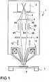
- the column 1 for a charged particle beam devicecomprises a charged particle source 2 which emits a beam 4 of charged particles.
- electron sourcessuch as Tungsten-Hairpin guns, Lanthanum-Hexaboride Guns, Field emission guns etc. can be used.
- the inventionis not limited to electron sources; it can be used together with all kinds of charged particle sources.
- the charged particlesare accelerated by an accelerating voltage supplied to the charged particle source 2.
- the charged particle beam 4After leaving the charged particle source 2, the charged particle beam 4 passes through an aperture plate 5 having multiple apertures 5A - 5H which are situated along a ring on the aperture plate 5. By passing through the aperture plate 5, multiple charged particle beams 4A - 4H are created. Thereafter, a deflector 6 is used to influence the beams of charged particles 4A - 4H so that each beam 4A - 4H appears to come from a different source.
- the deflector 6has the form of a cylinder lens comprising two cylinder electrodes 6A and 6B which are set to appropriate potentials. For example, the potential difference between the inner cylinder electrode 6A and the outer cylinder electrode 6B is set to +300 Volts so that the beams of charged particles 4A - 4H are attracted towards the inner cylinder electrode 6A.
- the charged particle beams 4A - 4Hthen pass the detector 9 which is used to detect those particles that come from the specimen 8 in order to produce multiple images of the specimen 8.
- the detector 9is divided in multiple segments 9A - 9H corresponding to the multiple beams of charged particles 4A - 4H. Thereby, each segment 9A - 9H of the detector is capable of detecting particles that come from the specimen 8 independent of all the other segments of the detector 9. Furthermore, the detector 9 comprises multiple openings to let the beams of charged particles 4A - 4H pass through.
- the detector 9is followed by the scanning coils 12 which are used to move the charged particle beams 4A - 4H in a raster over the surface of the specimen 8.
- the charged particle beams 4A - 4Henter the objective lens 10 that focuses the charged particle beams 4A - 4H onto the specimen 8.
- the objective lens 10not only focuses the charged particle beams 4A - 4H but also rotates the charged particle beams 4A - 4H. However, this effect is not shown because it is difficult to depict in a two-dimensional drawing and because the skilled person is well aware of this additional effect.
- a secondary product of major importance to examination or the image formation of specimensare secondary electrons that escape from the specimen 8 at a variety of angles with relatively low energy (3 to 50 eV). The secondary electrons are drawn through the objective lens 10, reach the detector 9, and are then measured.
- the parameters of the objective lens 10are chosen in such a manner that the secondary electrons and/or backscattered particles that come from specimen are focused onto the detector 9. Accordingly, each spot on the specimen leads to a corresponding spot on the detector. Thereby, the segments 9A - 9H of the detector 9 are selected so that each spot basically hits the corresponding segment 9A - 9H in its center.
- the embodiment shown in Fig. 1contains an objective lens 10 which is a combination of a magnetic lens 10A and an electrostatic lens 10B.
- the objective lens 10is a compound magnetic-electrostatic lens.
- the electrostatic part of the compound magnetic-electrostatic lens 10is an electrostatic retarding lens 10B.
- Using such a compound magnetic-electrostatic lens 10yields superior resolution at low acceleration energies, such as a few hundred electron volts in the case of a SEM. Such low acceleration energies are desirable, especially in modem semiconductor industry, to avoid charging and/or damaging of radiation sensitive specimens.
- the benefits of the present inventionare also achieved if only a magnetic lens or only an electrostatic lens is used.
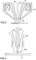
- Figures 2 and 3show enlarged views on the compound magnetic-electrostatic lens 10 and the specimen 8 as shown in Fig. 1 .
- the magnetic flux generated by a current through an excitation coilis conducted through pole pieces and is concentrated into a small region along the optical axis of the magnetic lens.
- the magnetic fieldis rotationally symmetric around the optical axis and reaches its maximum value in the pole gap between the upper and the lower pole piece.
- the embodiment shown in Figs. 1 to 3contains an electrostatic retarding lens which is situated close to magnetic lens 10A.
- the electrostatic retarding lens 10Bhas two electrodes held at different potentials.
- one of the two electrodesis formed by a cylindrical beam tube 14 which is arranged within the magnetic lens 10A along the optical axis.
- the second electrode of the electrostatic retarding lens 10Bis a metallic cup provided below the magnetic lens 10A.
- the first electrodeis usually held at high positive potential, for example 8 kV, where as the second electrode is held at lower positive potential, for example 3 kV, so that the electrons are decelerated in the corresponding electrostatic field from a first energy to a lower second energy.
- the specimen 8is held at ground potential. Accordingly, there is a further electrostatic retarding field between the metallic cup and the specimen 8.
- the surface of the specimenneed not be grounded.
- the electric potential on the surface of the specimenmay also be adjusted by applying a voltage to the specimen.
- a voltagecan be applied to a wafer, for example, in order to obtain voltage contrast imaging which is used to detect shorts in a circuit.
- an electrostatic retarding fieldis produced.
- the secondary electronsbackscattered particles
- Fig. 4shows schematically a top view on the aperture plate 5 as used in the column shown in Fig. 1 .
- the aperture plate 5comprises eight apertures 5A - 5H which are situated along a ring parallel to the edge of the aperture plate 5.
- the aperture plate 5is made of conducting material in order to avoid any charging effects.
- the size of the apertures 5A - 5His selected so that a predetermined current can be provided.
- Fig. 5shows schematically a top view on the deflector 6 as used in the column shown in Fig. 1 .
- the deflector 6has the form of a cylinder lens comprising two cylinder electrodes 6A and 6B which are set to appropriate potentials.
- a potential difference between the inner cylinder electrode 6A and the outer cylinder electrode 6Bis provided.
- the appropriate potential difference between the inner cylinder electrode 6A and the outer cylinder electrode 6Bdepends on a number of different parameters, for example the energy of the charged particles inside the deflector 6 or the desired distance between two adjacent beams on the surface of the specimen.
- the potential differencelies in the range of 100 to 500 Volts.
- Fig. 6shows schematically a bottom view on the detector 9 as used in the column shown in Fig. 1 .
- the detector 9is divided in multiple segments 9A - 9H each having the form of a piece of cake and each corresponding to one of charged particle beams 4A - 4H.
- each segment 9A - 9H of the detectoris capable of detecting particles that come from the specimen 8 independent of all the other segments of the detector 9.
- detector 9comprises multiple openings 11A - 11H to let the beams of charged particles 4A - 4H pass through.
- the detector 9is orientated in such a manner so that each spot on the specimen is focused to the center of the corresponding segment 9A - 9H.
- Fig. 7shows schematically a column according to a second embodiment of the present invention. This embodiment is similar to that of Figure 1 , except for the following;
- the columncomprises a beam selector 16 located right after the particle source 2.
- the beam selector 16comprises a first deflector 16A, aperture plate 16B, a second deflector 16C, and a third deflector 16D.
- the aperture plate 16Bcomprises two apertures having two different diameters. After the beam of charged particles leaves the particle source 2, the first deflector 16A deflects the charged particle beam 4 towards one the two aperture in the aperture plate 1&B. Thereafter, the second and the third deflector bring the charged particle beam 4 back to its way along the optical axis of the column.
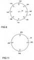
- the aperture plate 15 used in Fig. 7comprises, in addition to the apertures 15A - 15H situated along a ring parallel to the edge of the aperture plate, a further aperture 15I situated in the center of the aperture plate (see Fig. 8 ). Accordingly, a further beam of charged particles 4I is produced along the optical axis of the column.
- the detector 19also contains an additional opening 11I in order to let the beam 4I of charged particles pass through the detector 19 (see Fig. 9 ).
- the resulting beam 4will be so small that the apertures 15A - 15H situated along the ring parallel to the edge of the aperture plate are not illuminated by charged particle beam 4. Accordingly, only charged particle beam 41 is formed.
- the charged particle beam 4Ipasses through the center of the inner electrode 6A without being affected by the field of the cylinder lens 6. Furthermore, the charged particle beam 4I passes through the detector 19 and is focused onto the specimen. Since there are no further charged particle beams, the column basically functions as a conventional single beam device.
- the resulting beam 4will be large enough so that the apertures 15A - 15H situated along the ring parallel to the edge of the aperture plate are illuminated by charged particle beam 4. Accordingly, all charged particle beams 4A - 4I are formed.
- the column shown in Fig. 7basically operates as the column shown in Fig. 1 . Since, in this mode, the parameters of the objective lens 10 are chosen in such a manner that the secondary electrons and/or backscattered particles that come from specimen are focused onto the detector 19, the secondary electrons corresponding to the center beam 4I are focused on the center of the detector 19. Accordingly, these electrons are not measured by the detector 19.
- the operatormay switch easily between two modes of operation. Accordingly, the device shown in Fig. 7 can be adapted in a fast and efficient manner to the specific measurement needs.
- Fig. 10shows schematically a column according to a third embodiment of the present invention. This embodiment is also similar to that of Figure 1 , except for the following;
- the charged particle beam 4passes through the aperture plate 25 having four apertures 25A - 25D which are situated at equal distance along a ring on the aperture plate 25.
- four charged particle beams 4A - 4Dare created.
- the deflectors 26A - 26Dare used to influence the beams of charged particles 4A - 4D so that each beam 4A - 4D appears to come from a different source.
- the deflectors 26A - 26Dinfluence each of the beams 4A - 4D individually which leads to a better control of the properties of each individual beam
- the charged particle beams 4A - 4Dthen pass the detector 29 which is used to detect those particles that come from the specimen 8 in order to produce multiple images of the specimen 8.
- the detector 29is divided in multiple segments 29A - 29D corresponding to the multiple beams of charged particles 4A - 4D (see Fig. 13 ). Thereby, each segment 29A - 29D of the detector is capable of detecting particles that come from the specimen 8 independent of all the other segments of the detector 29.
- detector 29comprises multiple openings to let the beams of charged particles 4A - 4D pass through.
- Fig. 12shows schematically a top view on the deflectors 26A - 26D as used in the column shown in Fig. 10 .
- each deflector 26A - 26Dcomprises eight electrodes.
- Each deflector 26A - 26Dgenerates static deflecting fields for correction of the beam paths through the objective lens and for positioning the beams at the specimen.
- the deflectors 26A - 26Dcan be used for compensation of the aberrations arising from a deviation of the objective lens from the axial symmetry.
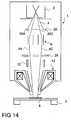
- Fig. 14shows schematically a column according to a third embodiment of the present invention. This embodiment is also similar to that of Figure 1 , except for the following;
- the charged particle beam 4passes through the aperture plate 25 having four apertures 25A - 25D which are situated at equal distance along a ring on the aperture plate 25.
- the deflector 6is used to influence the beams of charged particles 4A - 4D so that each beam 4A - 4D appears to come from a different source.
- the deflector 6is used to influence the beams of charged particles 4A - 4D so that each beam 4A - 4D traverses the objective lens 10 along an off-axis path. Due to the off-axis path of the charged particle beams 4A - 4D, the beams are tilted and hit the specimen under oblique angles of incidence.
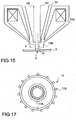
- Fig. 15shows an enlarged view on the compound magnetic-electrostatic lens 10 and the specimen 8 as shown in Fig. 14 .
- the beam 4Ahits the specimen 8 under an oblique angle of incidence - ⁇ , as measured with regard to an axis normal to the surface of the specimen.
- the beam 4Chits the specimen 8 under an oblique angle of incidence + ⁇ .
- the electron beams 4A and 4Cdo not hit the specimen at the same spot but are displaced from each other by a distance D.
- the images from the two beams 4A and 4Care recorded. Based on the fact that beams hit the specimen under different angles of incidence, the images of the two beams are sufficient to produce a stereoscopic image of the surface of specimen.
- the electrostatic retarding lens 10Bhas two electrodes held at different potentials.
- one of the two electrodesis formed by a cylindrical beam tube 14 which is arranged within the magnetic lens 10A along the optical axis.
- the second electrode of the electrostatic retarding lens 10Bis a metallic cup provided below the magnetic lens 10A.
- the first electrodeis usually held at high positive potential, for example 8 kV, where as the second electrode is held at lower positive potential, for example 3 kV, so that the electrons are decelerated in the corresponding electrostatic field from a first energy to a lower second energy.
- the specimen 8is held at ground potential. Accordingly, there is a further electrostatic retarding field between the metallic cup and the specimen 8. Due to the electrostatic retarding field between the metallic cup and the specimen 8, the initial tilt of the charged particle beams 4A - 4D caused by the off-axis path of the charged particle beams 4A - 4D is enhanced leading to increased angles of incidence.
- the surface of the specimenneed not be grounded.
- the electric potential on the surface of the specimenmay also be adjusted by applying a voltage to the specimen. A voltage can be applied to a wafer, for example, in order to obtain voltage contrast imaging which is used to detect shorts in a circuit. As long as the potential of the metallic cup is higher than the potential on the surface of the specimen 8, an electrostatic retarding field is produced.
- stereoscopic images of the surfacecan be made in a single scan. Accordingly, stereoscopic images of a specimen can be produced in a fast and reliable manner without the need for any additional alignments. Therefore, the additional information, which is contained in stereo images and which is extremely helpful in many cases, can be accessed without causing any additional costs and without causing any additional time delays.
- the embodiment shown in Fig. 14uses the off-axis path of the beams through the objective lens 10 in order to tilt the beams 4A - 4D.
- the off-axis path of the beams through the objective lens 10gives rise to chromatic aberrations.
- the charged particles, usually electron, in the beamsare not monochromatic, but are emitted with slightly different energies.
- the energy spreadi.e., the full width at half maximum of the electron energy distribution
- T cis the temperature of the cathode tip and k is Boltzmann's constant.
- Fig. 16shows a schematic diagram of an apparatus according to a further embodiment of the present invention. This embodiment is similar to that of Fig. 10 , except for the following.
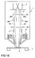
- the deflector 6has been replaced by an integrated unit 17 comprising a deflector 17A and a coil arrangement 17B (see Fig. 17 ).
- the deflector 17A and the coil arrangement 17Bgenerate crossed electrostatic and magnetic deflection fields which disperse the beams 4A - 4D of charged particles.
- a second chromatic aberrationof substantially the same kind and magnitude but opposite direction as the chromatic aberration caused off-axis path of the beams through the objective lens can be produced. Accordingly, the chromatic aberration caused by the off-axis path can be compensated in the plane of the specimen surface.
- Fig. 17shows schematically a top view on the unit 17 as used in the column shown in Fig. 16 .
- the unit 17comprises a deflector 17A having the form of a cylinder lens.
- the cylinder deflector 17Acomprises two cylinder electrodes which are set to appropriate potentials.
- a potential difference between the inner cylinder electrode and the outer cylinder electrodeis provided in order to attract the charged particle beams 4A - 4D towards the inner cylinder electrode.
- the potential difference between the inner cylinder electrode and the outer cylinder electrodeis chosen in such a manner that the beam pass through the objective lens along an off-axis path and hits the specimen under oblique angles of incidence.
- the appropriate potential difference between the inner cylinder electrode 6A and the outer cylinder electrode 6Bdepends on a number different parameters; for example, the energy of the charged particles inside the deflector 6, the desired distance between two adjacent beams on the surface of the specimen, and the angles of incidence on the surface of the specimen.
- the potential differencelies in the range of 100 to 500 Volts.
- the unit 17comprises a coil arrangement 17B which is used to generate a magnetic field within cylinder deflector 17A.
- the magnetic fieldis essentially perpendicular to the electric filed generated by the inner cylinder electrode and the outer cylinder electrode.
- the dispersionleads to an at least partial compensation of the chromatic aberration caused by the off-axis pass through the objective lens.
- the embodiment shown in Fig. 16has thus the advantage that large angles of incidence on the sample surface can be provided without reduction in resolution arising from large chromatic aberrations.
- Fig. 18shows schematically a column according to a still further embodiment according to the present invention. This embodiment is similar to that of Figure 16 , except for the following; After passing through the aperture plate 25 four charged particle beams 4A - 4D enter the compensation units 36A - 36D.
- the compensation units 36A - 36Dare again used to influence the beams of charged particles 4A - 4D so that each beam 4A - 4D appears to come from a different source.
- the compensation units 36A - 36Dare used to influence the beams of charged particles 4A - 4D so that each beam 4A - 4D traverses the objective lens 10 along an off-axis path.
- the compensation units 36A - 36Dinfluence each of the beams 4A - 4D individually which leads to a better control of the properties of each individual beam
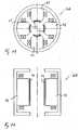
- Figs. 19 and 20show the compensation unit 36A used in Fig. 18 .
- the compensation unit 36Aforms a Wien filter having an electrostatic and magnetic quadrupole (4-pole).
- the quadrupolecomprises four pole pieces 42 and four electrodes 44.
- the electrodes and pole piecesare arranged in a plane perpendicular to the path of the charged particles.
- the electrodes and the pole piecesare each placed along the circumference of a circle, spaced by an angle of ⁇ /2. Since the pole pieces and the corresponding electrodes have the same length ( Fig. 20 ) and almost the same radius ( Fig. 19 ), the resulting electric and magnetic field distributions are very similar leading to a good compensation of the electric and magnetic forces for the electrons with predetermined energy in any point along the optical axis of the Wien filter.
- magnetic and electrostatic fieldscan be adjusted to deflect in an arbitrary direction in the plane perpendicular to the optical axis. Thereby, a compensation can be achieved for any direction of the deflecting action.
Landscapes
- Chemical & Material Sciences (AREA)
- Analytical Chemistry (AREA)
- Analysing Materials By The Use Of Radiation (AREA)
- Testing Or Measuring Of Semiconductors Or The Like (AREA)
Description
- The invention relates to an apparatus for the examination of specimen with charged particles. In particular, this invention relates to an apparatus for the examination of specimen with multiple beams of charged particles.
- Modem semiconductor technology is highly dependent on an accurate control of the various processes used during the production of integrated circuits. Accordingly, the wafers have to be inspected repeatedly in order to localize problems as early as possible. Furthermore, a mask or reticle should also be inspected before its actual use during wafer processing in order to make sure that the mask accurately defines the desired pattern. This is done because any defects in the mask pattern will be transferred to the substrate (e.g., wafer) during its use in microlithography. However, the inspection of wafers or masks for defects requires the examination of the whole wafer or mask area. Especially, the inspection of wafers during their fabrication requires the examination of the whole wafer area in such a short time that production throughput is not limited by the inspection process.
- Scanning electron microscopes (SEM) have been used to inspect wafers to detect pattern defects. Thereby, the surface of the wafer is scanned using a single finely drawn electron beam. When the electron beam hits the wafer, secondary electrons are generated and measured. A pattern defect at a location on the wafer is detected by comparing an intensity signal of the secondary electrons to, for example, a reference signal corresponding to the same location on the pattern. However, because only one very narrow electron beam is used for scanning, a long time is required to scan the entire surface of the wafer. Accordingly, it is not feasible to use a conventional (single-beam) Scanning Electron Microscope (SEM) for wafer inspection, since this approach does not provide the required throughput. Therefore, high speed wafer inspection is presently carried out by means of light optical techniques.
- In order to perform this task using electron microscopic techniques several approaches have been suggested. One approach is based on the miniaturization of SEMs, so that several miniaturized SEMs (in the order of ten to one hundred) are arranged in an array and each miniaturized SEM examines a small portion of the complete sample surface. Another approach makes use of fixed-beam surface electron microscopes which image a certain area of the sample simultaneously. These surface microscopes can be classified by the excitation process of the electrons that form the image at the detector: a) The Photoemission Electron Microscope (PEEM), where the electrons are created by illumination of the sample surface with UV light, synchrotron radiation, or X-rays and b) the so-called Low-energy Electron Microscope (LEEM), where, in various modes of operation, the sample surface is illuminated with electrons. In this case, the illuminating electrons have to be separated from the imaging electrons by means of an additional electron optical element, for example, a beam separator in the form of a dipole magnet. However, both approaches have not yet been put into industrial practice.
- Multi-beam electron projection systems are used to create patterns of variable shape on a substrate by switching on and off individual beams as is described in
document EP 0 508 151 . The following remarks are particularly relevant: First, as a projection system, it inherently does not produce an image of a sample and, therefore, does not comprise an objective lens. Secondly, in the example to which we referred to above, a resulting electron beam, formed by the individual beams that are not blanked out, is scanned as a whole over the substrate. - Furthermore, SEMs using multiple charged particle beams have been suggested in order to increase the throughput of data collection process. For example,
US Patent 5,892,224 describes an apparatus for inspecting masks and wafers used in microlithography. The apparatus according toUS Patent 5,892,224 is adapted to irradiate multiple charged particle beams simultaneously on respective measurement points on the surface of a sample. However, the apparatus according toUS Patent 5,892,224 is primarily designed for the inspection of masks and does not provide the resolution which is required to inspect the intricate features present on a semiconductor wafer. - In charged particle beam devices, such as a scanning electron microscope (SEM), the charged particle beam exhibits a typical aperture angle as well as a typical angle of incidence in the order of several millirads. However, for many applications, it is desirable that the charged particle beam hits the sample surface under a much larger angle of typically 5° to 10°, corresponding to 90 to 180 millirads. Stereoscopic visualization is an example of such an application. Some applications even require tilt angles in excess of 15° or even 20°. In many cases, the additional information which is contained in stereo images is extremely valuable in order to control the quality of a production process.
- Thereby, a number of tilting mechanism can be used. In early solutions, an oblique angle of incidence was achieved by mechanically tilting the specimen. However, apart from other drawbacks, mechanically tilting the specimen takes a lot of time. An oblique angle of incidence may also be achieved by electrically tilting the charged particle beam. This can be done by deflecting the beam so that either by the deflection alone or in combination with the focussing of the beam, an oblique angle of incidence results. Thereby, the specimen can remain horizontal which is a significant advantage as far as the lateral coordinate registration is concerned. Furthermore, electrical tilting is also much faster than its mechanical counterpart. However, even though electrical tilting is in principal faster than its mechanical counterpart, additional alignment procedures are usually required when the beam is shifted electrically from angle of incidence to another angle of incidence. These additional alignment also require a considerable amount time. Therefore, stereoscopic visualization is not routinely done in the semiconductor industry.
GB 2 340 991 A- Further,
US 4,209 698 describes a transmission-type charged particle beam apparatus comprising a vacuum envelope enclosing and means having at least ten individual charged particle sources to separately produce at least ten individual charged particle beams. Further,GB 2 071 403JP 10 062 503 - Accordingly, there is a need for a charged particle beam device which provides a sufficient resolution and which is able to increase the data collection to such an extent that the device can also be applied to high speed wafer inspection. Furthermore, there is a need for a charged particle beam device which is able to reduce the time that is needed to produce a pair of stereo images.
- The present invention provides an improved column for a charged particle beam device. According to the present invention, there is provided a column for a charged particle beam device as specified in
independent claim 1. Further advantageous features, aspects and details of the invention are evident from the dependent claims, the description and the accompanying drawings. - The present invention provides an improved column for a charged particle beam device. The column comprises an aperture plate having multiple apertures to produce multiple beams of charged particles and a deflector to influence the beams of charged particles so that each beam appears to come from a different source. Furthermore, an objective lens is used in order to focus the charged-particle beams onto the specimen. Due to the deflector and the apertures, multiple images of the source are created on the surface of the specimen whereby all the images can be used for parallel data acquisition and/or for parallel modification of the specimen. Accordingly, the speed of data acquisition (modification) is increased. With regard to the focusing properties of the objective lens, the beams of charged particles can basically be treated as independent particle beams which do not negatively affect each other. Accordingly, each beam basically provides the same resolution as the beam a conventional charged particle beam device.
- Preferably, an improved column for a charged particle beam device is provided which is capable of producing a stereoscopic image of the surface of specimen in a single scan over the surface of specimen. The column comprises an aperture plate having multiple apertures to produce multiple beams of charged particles and a deflector to influence the beams of charged particles so that each beam appears to come from a different source and that each beam passes through the objective lens along an off-axis path. Due to the off-axis path through the objective lens, the charged particle beams are tilted and hit the specimen under oblique angle of incidences. Furthermore, each beam is tilted into a different direction so that the images of two of the beams are sufficient to produce a stereoscopic image of the surface of specimen. Since there no need for any additional alignments of beams with regard to the column, the time that is required to produce a stereoscopic image is reduced considerably.
- Some of the above indicated and other more detailed aspects of the invention will be described in the following description and partially illustrated with reference to the figures. Therein:
- Fig. 1
- shows schematically a column according to a first embodiment according to the present invention,
- Fig. 2
- is an enlarged view showing the objective lens of the embodiment of
Fig. 1 . - Fig. 3
- is an enlarged view of
Fig. 2 . - Fig. 4
- shows schematically the aperture plate as used in the column shown in
Fig. 1 , - Fig. 5
- shows schematically a top view on the cylinder lens as used in the column shown in
Fig. 1 , - Fig. 6
- shows schematically a bottom view on the detector as used in the column shown in
Fig. 1 , - Fig. 7
- shows schematically an column according to a second embodiment according to the present invention
- Fig. 8
- shows schematically the aperture plate as used in the column shown in
Fig. 7 , - Fig. 9
- shows schematically a bottom view on the detector used in the column shown in
Fig. 7 , - Fig. 10
- shows schematically a column according to a third embodiment according to the present invention,
- Fig. 11
- shows schematically the aperture plate as used in the column shown in
Fig. 10 , - Fig. 12
- shows schematically a top view on the deflectors as used in the column shown in
Fig. 10 , - Fig. 13
- shows schematically a bottom view on the detector as used in the column shown in
Fig. 10 , - Fig. 14
- shows schematically a column according to a fourth embodiment according to the present invention,
- Fig. 15
- is an enlarged view showing the objective lens of the embodiment of
Fig. 14 , - Fig. 16
- shows schematically a column according to a fifth embodiment according to the present invention,
- Fig. 17
- shows schematically a top view on the compensation unit as used in the column shown in
Fig. 16 , - Fig. 18
- shows schematically a column according to a further embodiment according to the present invention,
- Fig. 19,20
- show schematically a top view and a side view on the compensation unit as used in the column shown in
Fig. 18 , - An embodiment according to the invention is shown schematically in
Fig. 1 . Thecolumn 1 for a charged particle beam device comprises a chargedparticle source 2 which emits abeam 4 of charged particles. In electron beam devices, electron sources such as Tungsten-Hairpin guns, Lanthanum-Hexaboride Guns, Field emission guns etc. can be used. The invention, however, is not limited to electron sources; it can be used together with all kinds of charged particle sources. The charged particles are accelerated by an accelerating voltage supplied to the chargedparticle source 2. - After leaving the charged
particle source 2, the chargedparticle beam 4 passes through anaperture plate 5 havingmultiple apertures 5A - 5H which are situated along a ring on theaperture plate 5. By passing through theaperture plate 5, multiple chargedparticle beams 4A - 4H are created. Thereafter, adeflector 6 is used to influence the beams of chargedparticles 4A - 4H so that eachbeam 4A - 4H appears to come from a different source. In the present embodiment thedeflector 6 has the form of a cylinder lens comprising twocylinder electrodes inner cylinder electrode 6A and theouter cylinder electrode 6B is set to +300 Volts so that the beams of chargedparticles 4A - 4H are attracted towards theinner cylinder electrode 6A. - The charged
particle beams 4A - 4H then pass the detector 9 which is used to detect those particles that come from thespecimen 8 in order to produce multiple images of thespecimen 8. The detector 9 is divided inmultiple segments 9A - 9H corresponding to the multiple beams of chargedparticles 4A - 4H. Thereby, eachsegment 9A - 9H of the detector is capable of detecting particles that come from thespecimen 8 independent of all the other segments of the detector 9. Furthermore, the detector 9 comprises multiple openings to let the beams of chargedparticles 4A - 4H pass through. - The detector 9 is followed by the scanning coils 12 which are used to move the charged
particle beams 4A - 4H in a raster over the surface of thespecimen 8. After the scanning coils 12, the chargedparticle beams 4A - 4H enter theobjective lens 10 that focuses the chargedparticle beams 4A - 4H onto thespecimen 8. Theobjective lens 10 not only focuses the chargedparticle beams 4A - 4H but also rotates the chargedparticle beams 4A - 4H. However, this effect is not shown because it is difficult to depict in a two-dimensional drawing and because the skilled person is well aware of this additional effect. Due to the combined effects of thedeflector 6 and theobjective lens 10, multiple spots (images of the particle source 2), each corresponding to one of the chargedparticle beams 4A - 4H, are created on thespecimen 8. Without thedeflector 6, theobjective lens 10 would focus the chargedparticle beams 4A - 4H into a single spot on thespecimen 8. - When the particles of
beams 4A - 4H strike the surface of thespecimen 8, they undergo a series of complex interactions with the nuclei and electrons of the atoms of the specimen. The interactions produce a variety of secondary products, such as electrons of different energy, X rays, heat, and light. Many of these secondary products are used to produce the images of the sample and to collect additional data from it. A secondary product of major importance to examination or the image formation of specimens are secondary electrons that escape from thespecimen 8 at a variety of angles with relatively low energy (3 to 50 eV). The secondary electrons are drawn through theobjective lens 10, reach the detector 9, and are then measured. Thereby, the parameters of theobjective lens 10 are chosen in such a manner that the secondary electrons and/or backscattered particles that come from specimen are focused onto the detector 9. Accordingly, each spot on the specimen leads to a corresponding spot on the detector. Thereby, thesegments 9A - 9H of the detector 9 are selected so that each spot basically hits the correspondingsegment 9A - 9H in its center. - By scanning the charged
particle beams 4A - 4H over the specimen and displaying/recording the output of the detector 9, multiple independent images of the surface of thespecimen 8 are formed. Each image contains information about a different portion of the surface of the specimen. Accordingly, the speed of the data acquisition is increased by afactor 8 with regard to the conventional single beam case. Thespecimen 8 is supported on a stage 7 (specimen support) which is moveable horizontally in all directions, in order to allow the chargedparticle beams 4A - 4H to reach the target areas on the specimen which are to be examined. - In order to improve the performance of the system, the embodiment shown in
Fig. 1 contains anobjective lens 10 which is a combination of amagnetic lens 10A and anelectrostatic lens 10B. Accordingly, theobjective lens 10 is a compound magnetic-electrostatic lens. Preferably, the electrostatic part of the compound magnetic-electrostatic lens 10 is anelectrostatic retarding lens 10B. Using such a compound magnetic-electrostatic lens 10 yields superior resolution at low acceleration energies, such as a few hundred electron volts in the case of a SEM. Such low acceleration energies are desirable, especially in modem semiconductor industry, to avoid charging and/or damaging of radiation sensitive specimens. However, the benefits of the present invention are also achieved if only a magnetic lens or only an electrostatic lens is used. Figures 2 and 3 show enlarged views on the compound magnetic-electrostatic lens 10 and thespecimen 8 as shown inFig. 1 . To achieve a small focal length, the magnetic flux generated by a current through an excitation coil is conducted through pole pieces and is concentrated into a small region along the optical axis of the magnetic lens. The magnetic field is rotationally symmetric around the optical axis and reaches its maximum value in the pole gap between the upper and the lower pole piece. In addition to themagnetic lens 10A, the embodiment shown inFigs. 1 to 3 contains an electrostatic retarding lens which is situated close tomagnetic lens 10A. Theelectrostatic retarding lens 10B has two electrodes held at different potentials. In the illustrated embodiment, one of the two electrodes is formed by acylindrical beam tube 14 which is arranged within themagnetic lens 10A along the optical axis. The second electrode of theelectrostatic retarding lens 10B is a metallic cup provided below themagnetic lens 10A. In operation of the system, the first electrode is usually held at high positive potential, for example 8 kV, where as the second electrode is held at lower positive potential, for example 3 kV, so that the electrons are decelerated in the corresponding electrostatic field from a first energy to a lower second energy.- In the example shown in
Figs 2 and 3 , thespecimen 8 is held at ground potential. Accordingly, there is a further electrostatic retarding field between the metallic cup and thespecimen 8. However, the surface of the specimen need not be grounded. The electric potential on the surface of the specimen may also be adjusted by applying a voltage to the specimen. A voltage can be applied to a wafer, for example, in order to obtain voltage contrast imaging which is used to detect shorts in a circuit. As long as the potential of the metallic cup is higher than the potential on the surface of the specimen, an electrostatic retarding field is produced. Furthermore, as long as the potential of the metallic cup is higher than the potential on the surface of the specimen, the secondary electrons (backscattered particles) are drawn into theobjective lens 10 and reach the detector 9. Fig. 4 shows schematically a top view on theaperture plate 5 as used in the column shown inFig. 1 . Theaperture plate 5 comprises eightapertures 5A - 5H which are situated along a ring parallel to the edge of theaperture plate 5. Theaperture plate 5 is made of conducting material in order to avoid any charging effects. The size of theapertures 5A - 5H is selected so that a predetermined current can be provided.Fig. 5 shows schematically a top view on thedeflector 6 as used in the column shown inFig. 1 . Thedeflector 6 has the form of a cylinder lens comprising twocylinder electrodes particle beams 4A - 4H towards theinner cylinder electrode 6A, a potential difference between theinner cylinder electrode 6A and theouter cylinder electrode 6B is provided. The appropriate potential difference between theinner cylinder electrode 6A and theouter cylinder electrode 6B depends on a number of different parameters, for example the energy of the charged particles inside thedeflector 6 or the desired distance between two adjacent beams on the surface of the specimen. Usually, the potential difference lies in the range of 100 to 500 Volts.Fig. 6 shows schematically a bottom view on the detector 9 as used in the column shown inFig. 1 . The detector 9 is divided inmultiple segments 9A - 9H each having the form of a piece of cake and each corresponding to one of chargedparticle beams 4A - 4H. Thereby, eachsegment 9A - 9H of the detector is capable of detecting particles that come from thespecimen 8 independent of all the other segments of the detector 9. Furthermore, detector 9 comprisesmultiple openings 11A - 11H to let the beams of chargedparticles 4A - 4H pass through. The detector 9 is orientated in such a manner so that each spot on the specimen is focused to the center of the correspondingsegment 9A - 9H.Fig. 7 shows schematically a column according to a second embodiment of the present invention. This embodiment is similar to that ofFigure 1 , except for the following; The column comprises abeam selector 16 located right after theparticle source 2. Thebeam selector 16 comprises afirst deflector 16A,aperture plate 16B, asecond deflector 16C, and athird deflector 16D. Theaperture plate 16B comprises two apertures having two different diameters. After the beam of charged particles leaves theparticle source 2, thefirst deflector 16A deflects the chargedparticle beam 4 towards one the two aperture in the aperture plate 1&B. Thereafter, the second and the third deflector bring the chargedparticle beam 4 back to its way along the optical axis of the column.- The
aperture plate 15 used inFig. 7 comprises, in addition to theapertures 15A - 15H situated along a ring parallel to the edge of the aperture plate, a further aperture 15I situated in the center of the aperture plate (seeFig. 8 ). Accordingly, a further beam of charged particles 4I is produced along the optical axis of the column. Thedetector 19 also contains an additional opening 11I in order to let the beam 4I of charged particles pass through the detector 19 (seeFig. 9 ). - If the charged particle beam is directed to the smaller aperture in the
aperture plate 16B, the resultingbeam 4 will be so small that theapertures 15A - 15H situated along the ring parallel to the edge of the aperture plate are not illuminated by chargedparticle beam 4. Accordingly, only charged particle beam 41 is formed. In the following, the charged particle beam 4I passes through the center of theinner electrode 6A without being affected by the field of thecylinder lens 6. Furthermore, the charged particle beam 4I passes through thedetector 19 and is focused onto the specimen. Since there are no further charged particle beams, the column basically functions as a conventional single beam device. - If the charged particle beam is directed to the larger aperture in the
aperture plate 16B, the resultingbeam 4 will be large enough so that theapertures 15A - 15H situated along the ring parallel to the edge of the aperture plate are illuminated by chargedparticle beam 4. Accordingly, all chargedparticle beams 4A - 4I are formed. In this mode, the column shown inFig. 7 basically operates as the column shown inFig. 1 . Since, in this mode, the parameters of theobjective lens 10 are chosen in such a manner that the secondary electrons and/or backscattered particles that come from specimen are focused onto thedetector 19, the secondary electrons corresponding to the center beam 4I are focused on the center of thedetector 19. Accordingly, these electrons are not measured by thedetector 19. - Due to the usage of the
beam selector 16, the operator may switch easily between two modes of operation. Accordingly, the device shown inFig. 7 can be adapted in a fast and efficient manner to the specific measurement needs. Fig. 10 shows schematically a column according to a third embodiment of the present invention. This embodiment is also similar to that ofFigure 1 , except for the following; After leaving the chargedparticle source 2, the chargedparticle beam 4 passes through theaperture plate 25 having fourapertures 25A - 25D which are situated at equal distance along a ring on theaperture plate 25. By passing through theaperture plate 25, four chargedparticle beams 4A - 4D are created. Thereafter, thedeflectors 26A - 26D are used to influence the beams of chargedparticles 4A - 4D so that eachbeam 4A - 4D appears to come from a different source. Thedeflectors 26A - 26D influence each of thebeams 4A - 4D individually which leads to a better control of the properties of each individual beam- The charged
particle beams 4A - 4D then pass thedetector 29 which is used to detect those particles that come from thespecimen 8 in order to produce multiple images of thespecimen 8. Thedetector 29 is divided inmultiple segments 29A - 29D corresponding to the multiple beams of chargedparticles 4A - 4D (seeFig. 13 ). Thereby, eachsegment 29A - 29D of the detector is capable of detecting particles that come from thespecimen 8 independent of all the other segments of thedetector 29. Furthermore,detector 29 comprises multiple openings to let the beams of chargedparticles 4A - 4D pass through. Fig. 12 shows schematically a top view on thedeflectors 26A - 26D as used in the column shown inFig. 10 . Thereby, eachdeflector 26A - 26D comprises eight electrodes. Eachdeflector 26A - 26D generates static deflecting fields for correction of the beam paths through the objective lens and for positioning the beams at the specimen. Furthermore, thedeflectors 26A - 26D can be used for compensation of the aberrations arising from a deviation of the objective lens from the axial symmetry.Fig. 14 shows schematically a column according to a third embodiment of the present invention. This embodiment is also similar to that ofFigure 1 , except for the following; After leaving the chargedparticle source 2 the chargedparticle beam 4 passes through theaperture plate 25 having fourapertures 25A - 25D which are situated at equal distance along a ring on theaperture plate 25. By passing through theaperture plate 25, four chargedparticle beams 4A - 4D are created. Thereafter, thedeflector 6 is used to influence the beams of chargedparticles 4A - 4D so that eachbeam 4A - 4D appears to come from a different source. Furthermore, thedeflector 6 is used to influence the beams of chargedparticles 4A - 4D so that eachbeam 4A - 4D traverses theobjective lens 10 along an off-axis path. Due to the off-axis path of the chargedparticle beams 4A - 4D, the beams are tilted and hit the specimen under oblique angles of incidence.Fig. 15 shows an enlarged view on the compound magnetic-electrostatic lens 10 and thespecimen 8 as shown inFig. 14 . Thereby, thebeam 4A hits thespecimen 8 under an oblique angle of incidence -θ, as measured with regard to an axis normal to the surface of the specimen. Furthermore, thebeam 4C hits thespecimen 8 under an oblique angle of incidence +θ. Theelectron beams beams beams - As outlined with regard to
Fig. 1 , theelectrostatic retarding lens 10B has two electrodes held at different potentials. In the illustrated embodiment, one of the two electrodes is formed by acylindrical beam tube 14 which is arranged within themagnetic lens 10A along the optical axis. The second electrode of theelectrostatic retarding lens 10B is a metallic cup provided below themagnetic lens 10A. In operation of the system, the first electrode is usually held at high positive potential, for example 8 kV, where as the second electrode is held at lower positive potential, for example 3 kV, so that the electrons are decelerated in the corresponding electrostatic field from a first energy to a lower second energy. - In the example shown in
Fig. 15 , thespecimen 8 is held at ground potential. Accordingly, there is a further electrostatic retarding field between the metallic cup and thespecimen 8. Due to the electrostatic retarding field between the metallic cup and thespecimen 8, the initial tilt of the chargedparticle beams 4A - 4D caused by the off-axis path of the chargedparticle beams 4A - 4D is enhanced leading to increased angles of incidence. The surface of the specimen need not be grounded. The electric potential on the surface of the specimen may also be adjusted by applying a voltage to the specimen. A voltage can be applied to a wafer, for example, in order to obtain voltage contrast imaging which is used to detect shorts in a circuit. As long as the potential of the metallic cup is higher than the potential on the surface of thespecimen 8, an electrostatic retarding field is produced. - By scanning the four
beams 4A - 4D over the surface of the specimen, stereoscopic images of the surface can be made in a single scan. Accordingly, stereoscopic images of a specimen can be produced in a fast and reliable manner without the need for any additional alignments. Therefore, the additional information, which is contained in stereo images and which is extremely helpful in many cases, can be accessed without causing any additional costs and without causing any additional time delays. - The embodiment shown in
Fig. 14 uses the off-axis path of the beams through theobjective lens 10 in order to tilt thebeams 4A - 4D. However, the off-axis path of the beams through theobjective lens 10 gives rise to chromatic aberrations. The charged particles, usually electron, in the beams are not monochromatic, but are emitted with slightly different energies. For example, in a thermionic electron gun, the energy spread (i.e., the full width at half maximum of the electron energy distribution) is on the order ofΔE = 2.5kTc, whereTc is the temperature of the cathode tip andk is Boltzmann's constant. This energy spread is further increased by the Boersch effect arising from space-charge oscillations near a crossover, so that thermionic tungsten cathodes show an energy spread ofΔE = 1 - 3 eV, while for LaB6 cathodes the value isΔE = 0.5 - 2 eV. Field emission guns usually have a lower energy spread due to the smaller cathode temperatures of the order ofΔE = 0.2 - 0.4 eV (L. Reimer, Scanning Electron Microscopy, Springer, 1985). - In order to decrease the chromatic aberrations,
Fig. 16 shows a schematic diagram of an apparatus according to a further embodiment of the present invention. This embodiment is similar to that ofFig. 10 , except for the following. Thedeflector 6 has been replaced by anintegrated unit 17 comprising adeflector 17A and acoil arrangement 17B (seeFig. 17 ). Thedeflector 17A and thecoil arrangement 17B generate crossed electrostatic and magnetic deflection fields which disperse thebeams 4A - 4D of charged particles. By dispersing the beams of charged particles a second chromatic aberration of substantially the same kind and magnitude but opposite direction as the chromatic aberration caused off-axis path of the beams through the objective lens can be produced. Accordingly, the chromatic aberration caused by the off-axis path can be compensated in the plane of the specimen surface. Fig. 17 shows schematically a top view on theunit 17 as used in the column shown inFig. 16 . Theunit 17 comprises adeflector 17A having the form of a cylinder lens. Thecylinder deflector 17A comprises two cylinder electrodes which are set to appropriate potentials. In order to attract the chargedparticle beams 4A - 4D towards the inner cylinder electrode, a potential difference between the inner cylinder electrode and the outer cylinder electrode is provided. Thereby, the potential difference between the inner cylinder electrode and the outer cylinder electrode is chosen in such a manner that the beam pass through the objective lens along an off-axis path and hits the specimen under oblique angles of incidence. The appropriate potential difference between theinner cylinder electrode 6A and theouter cylinder electrode 6B depends on a number different parameters; for example, the energy of the charged particles inside thedeflector 6, the desired distance between two adjacent beams on the surface of the specimen, and the angles of incidence on the surface of the specimen. Usually, the potential difference lies in the range of 100 to 500 Volts.- In addition to the
cylinder deflector 17A, theunit 17 comprises acoil arrangement 17B which is used to generate a magnetic field withincylinder deflector 17A. Thereby, the magnetic field is essentially perpendicular to the electric filed generated by the inner cylinder electrode and the outer cylinder electrode. Theintegrated unit 17 acts like a Wien filter, in which the electric field E and the magnetic fieldB generate an electric and a magnetic force on the charged particles,Fel = qE, andFmag = q (v xB), wherein q= -e is the electron charge. If the electric and magnetic field are perpendicular to each other and to the velocity of the charged particle, the electric and magnetic forces are in opposite directions. For particles with a certain velocity, ν = |E|/|B|, the net force is zero, and they pass the filter unaffected. Particles with a different speed experience a net force F = |Fel - Fmag| and are deflected by theunit 17. In effect, the beams of charged particles with a finite energy spread passing theunit 17 are dispersed, as particles with different energies are deflected by different amounts. - The dispersion leads to an at least partial compensation of the chromatic aberration caused by the off-axis pass through the objective lens. The embodiment shown in
Fig. 16 has thus the advantage that large angles of incidence on the sample surface can be provided without reduction in resolution arising from large chromatic aberrations. Fig. 18 shows schematically a column according to a still further embodiment according to the present invention. This embodiment is similar to that ofFigure 16 , except for the following; After passing through theaperture plate 25 four chargedparticle beams 4A - 4D enter thecompensation units 36A - 36D. Thecompensation units 36A - 36D are again used to influence the beams of chargedparticles 4A - 4D so that eachbeam 4A - 4D appears to come from a different source. Furthermore, thecompensation units 36A - 36D are used to influence the beams of chargedparticles 4A - 4D so that eachbeam 4A - 4D traverses theobjective lens 10 along an off-axis path. Thecompensation units 36A - 36D influence each of thebeams 4A - 4D individually which leads to a better control of the properties of each individual beamFigs. 19 and 20 show thecompensation unit 36A used inFig. 18 . Thecompensation unit 36A forms a Wien filter having an electrostatic and magnetic quadrupole (4-pole). The quadrupole comprises fourpole pieces 42 and fourelectrodes 44. The electrodes and pole pieces are arranged in a plane perpendicular to the path of the charged particles. As best shown inFig. 19 , the electrodes and the pole pieces are each placed along the circumference of a circle, spaced by an angle of π/2. Since the pole pieces and the corresponding electrodes have the same length (Fig. 20 ) and almost the same radius (Fig. 19 ), the resulting electric and magnetic field distributions are very similar leading to a good compensation of the electric and magnetic forces for the electrons with predetermined energy in any point along the optical axis of the Wien filter.- Using such a quadrupole arrangement, magnetic and electrostatic fields can be adjusted to deflect in an arbitrary direction in the plane perpendicular to the optical axis. Thereby, a compensation can be achieved for any direction of the deflecting action.
Claims (16)
- A column (1) for a charged particle beam device, which is used to examine and/or modify a specimen (8), said column comprising:a) a source (2) of charged-particles,b) an aperture plate (5) having at least two apertures (5A, 5E) to produce at least two beams (4A, 4E) of charged particles,c) at least one deflector (6) adapted to influence the beams of charged particles,d) at least one detector (9) adapted to measure secondary particles and/or backscattered particles coming from the specimen, ande) an objective lens (10) adapted to focus the charged-particle beams onto the specimen,characterized by that the detector (9) is positioned before the objective lens (10) and comprises multiple openings to let the beams of charged particles pass through, and wherein the objective lens (10) is adapted to focus the secondary particles and/or backscattered particles onto the detector (9).
- The column according to claim 1, wherein said deflector (6) comprises concentric cylinder electrodes.
- The column according to claim 1, wherein a deflector (6A, 6B) is provided for each individual beam.
- The column according to claim 3, wherein the deflectors (6A, 6B) are electrostatic multipoles, preferably selected from the group consisting of electrostatic dipole, quadrupole, hexapole and octupole.
- The column according to any of preceding claims, wherein the detector (9) is subdivided into multiple segments corresponding to the multiple beams of charged particles.
- The column according to any of preceding claims, wherein said objective lens (10) comprises a magnetic lens and an electrostatic lens.
- The column according to claim 6, wherein said column comprises a first electrode (14), means for applying a first potential to said first electrode, a second electrode (10B) and means for applying a second potential to said second electrode to generate an electrical field in said electrostatic lens (10) so that the particle beams in said electrical field are decelerated from a first energy to a second lower energy.
- The column according to any of preceding claims, wherein said apertures in said aperture plate (5) are arranged along at least one ring.
- The column according to any of preceding claims, wherein the column comprises a beam selector adapted to select the number of charged particle beams used to examine the specimen.
- The column according to any of preceding claims, wherein
the at least one deflector is adapted to influence the beams of charged particles so that by the combined action of the deflector and the objective lens the beams are tilted and hit the specimen with predetermined angles of incidence. - The column according to claim 10, wherein the column comprises a least one compensation unit (36A-36D) adapted to disperse the beams of charged particles, thereby compensating chromatic aberration in the plane of the specimen surface.
- The column according to claim 11, wherein the compensation unit (36A-36D) comprises means (42, 44) adapted to generate crossed electrostatic and magnetic deflection fields.
- The column according to one of claims 11 or 12, wherein the compensation (36A-36D) unit and the deflector (6) are integrated into one unit.
- The column according to claim 13, wherein the compensation unit (36A-36D) comprises concentric cylinder electrodes (44) and a coil arrangement.
- The column according to claim 13, wherein the compensation unit (36A-36D) is an electrostatic and magnetic multipole, preferably selected from the group consisting of electrostatic and magnetic dipole, quadrupole, hexapole and octupole.
- The column according to one of claims 10 to 15, wherein the column is adapted to provide angles of incidence between 2° and 15°, preferable between 3° and 10°.
Priority Applications (4)
| Application Number | Priority Date | Filing Date | Title |
|---|---|---|---|
| EP00108973.9AEP1150327B1 (en) | 2000-04-27 | 2000-04-27 | Multi beam charged particle device |
| PCT/EP2001/004787WO2001084592A1 (en) | 2000-04-27 | 2001-04-27 | Multi beam charged particle device |
| US10/258,869US6943349B2 (en) | 2000-04-27 | 2001-04-27 | Multi beam charged particle device |
| AU2001273976AAU2001273976A1 (en) | 2000-04-27 | 2001-04-27 | Multi beam charged particle device |
Applications Claiming Priority (1)
| Application Number | Priority Date | Filing Date | Title |
|---|---|---|---|
| EP00108973.9AEP1150327B1 (en) | 2000-04-27 | 2000-04-27 | Multi beam charged particle device |
Publications (2)
| Publication Number | Publication Date |
|---|---|
| EP1150327A1 EP1150327A1 (en) | 2001-10-31 |
| EP1150327B1true EP1150327B1 (en) | 2018-02-14 |
Family
ID=8168566
Family Applications (1)
| Application Number | Title | Priority Date | Filing Date |
|---|---|---|---|
| EP00108973.9AExpired - LifetimeEP1150327B1 (en) | 2000-04-27 | 2000-04-27 | Multi beam charged particle device |
Country Status (4)
| Country | Link |
|---|---|
| US (1) | US6943349B2 (en) |
| EP (1) | EP1150327B1 (en) |
| AU (1) | AU2001273976A1 (en) |
| WO (1) | WO2001084592A1 (en) |
Families Citing this family (83)
| Publication number | Priority date | Publication date | Assignee | Title |
|---|---|---|---|---|
| US6787772B2 (en)* | 2000-01-25 | 2004-09-07 | Hitachi, Ltd. | Scanning electron microscope |
| EP1150327B1 (en)* | 2000-04-27 | 2018-02-14 | ICT, Integrated Circuit Testing Gesellschaft für Halbleiterprüftechnik mbH | Multi beam charged particle device |
| US6946655B2 (en)* | 2001-11-07 | 2005-09-20 | Applied Materials, Inc. | Spot grid array electron imaging system |
| JP3968334B2 (en)* | 2002-09-11 | 2007-08-29 | 株式会社日立ハイテクノロジーズ | Charged particle beam apparatus and charged particle beam irradiation method |
| JP2006514408A (en)* | 2003-02-05 | 2006-04-27 | アプライド マテリアルズ イスラエル リミテッド | Method for measuring and reducing angular displacement of charged particle beams |
| TWM273099U (en)* | 2005-02-04 | 2005-08-11 | King Lion Entpr Co Ltd | Connector structure |
| NL1025500C2 (en)* | 2004-02-17 | 2005-08-19 | Fei Co | Particle source with selectable beam current and energy distribution. |
| EP1577926A1 (en)* | 2004-03-19 | 2005-09-21 | ICT, Integrated Circuit Testing Gesellschaft für Halbleiterprüftechnik Mbh | High current density particle beam system |
| JP4611755B2 (en)* | 2005-01-13 | 2011-01-12 | 株式会社日立ハイテクノロジーズ | Scanning electron microscope and imaging method thereof |
| US7394069B1 (en)* | 2005-08-30 | 2008-07-01 | Kla-Tencor Technologies Corporation | Large-field scanning of charged particles |
| US20090256075A1 (en) | 2005-09-06 | 2009-10-15 | Carl Zeiss Smt Ag | Charged Particle Inspection Method and Charged Particle System |
| EP1783811A3 (en)* | 2005-11-02 | 2008-02-27 | FEI Company | Corrector for the correction of chromatic aberrations in a particle-optical apparatus |
| US7276708B2 (en)* | 2005-11-23 | 2007-10-02 | Far-Tech, Inc. | Diagnostic resonant cavity for a charged particle accelerator |
| EP1801838B1 (en)* | 2005-12-20 | 2012-05-09 | ICT Integrated Circuit Testing Gesellschaft für Halbleiterprüftechnik mbH | Charged particle beam emitting device and method for operating a charged particle beam emitting device |
| EP2405458A1 (en)* | 2006-07-25 | 2012-01-11 | Mapper Lithography IP B.V. | A multiple beam charged particle optical system |
| US8134135B2 (en) | 2006-07-25 | 2012-03-13 | Mapper Lithography Ip B.V. | Multiple beam charged particle optical system |
| US7763851B2 (en)* | 2006-12-22 | 2010-07-27 | Ims Nanofabrication Ag | Particle-beam apparatus with improved wien-type filter |
| KR20090107536A (en) | 2007-01-22 | 2009-10-13 | 캘리포니아 인스티튜트 오브 테크놀로지 | Method for Quantitative 3-D Imaging |
| US8089635B2 (en) | 2007-01-22 | 2012-01-03 | California Institute Of Technology | Method and system for fast three-dimensional imaging using defocusing and feature recognition |
| AU2008244494B2 (en) | 2007-04-23 | 2010-10-21 | California Institute Of Technology | Single-lens 3-D imaging device using a polarization-coded aperture mask combined with a polarization-sensitive sensor |
| DE102008035297B4 (en)* | 2007-07-31 | 2017-08-17 | Hitachi High-Technologies Corporation | A charged particle beam aberration correcting device in an optical system of a charged particle beam device and a charged particle beam device having the aberration correcting device |
| US8642959B2 (en) | 2007-10-29 | 2014-02-04 | Micron Technology, Inc. | Method and system of performing three-dimensional imaging using an electron microscope |
| US8514268B2 (en)* | 2008-01-22 | 2013-08-20 | California Institute Of Technology | Method and device for high-resolution three-dimensional imaging which obtains camera pose using defocusing |
| EP2128885A1 (en)* | 2008-05-26 | 2009-12-02 | FEI Company | Charged particle source with integrated energy filter |
| US7932495B2 (en)* | 2008-09-02 | 2011-04-26 | ICT Integrated Circuit Testing Gesellschaft für Halbleiterprüftechnik mbH | Fast wafer inspection system |
| EP2226830B1 (en)* | 2009-03-06 | 2014-01-08 | FEI Company | Charged particle beam processing |
| SG10201401425RA (en) | 2009-04-13 | 2014-08-28 | Applied Materials Inc | Modification of magnetic properties of films using ion and neutral beam implantation |
| US8773507B2 (en)* | 2009-08-11 | 2014-07-08 | California Institute Of Technology | Defocusing feature matching system to measure camera pose with interchangeable lens cameras |
| US8773514B2 (en)* | 2009-08-27 | 2014-07-08 | California Institute Of Technology | Accurate 3D object reconstruction using a handheld device with a projected light pattern |
| EP2325862A1 (en) | 2009-11-18 | 2011-05-25 | Fei Company | Corrector for axial aberrations of a particle-optical lens |
| WO2011124352A1 (en)* | 2010-04-09 | 2011-10-13 | Carl Zeiss Smt Gmbh | Charged particle detection system and multi-beamlet inspection system |
| EP2378537B1 (en)* | 2010-04-19 | 2014-02-12 | ICT Integrated Circuit Testing Gesellschaft für Halbleiterprüftechnik mbH | Method of operating a charged particle beam device |
| EP2402475A1 (en) | 2010-06-30 | 2012-01-04 | Fei Company | Beam-induced deposition at cryogenic temperatures |
| JP6007178B2 (en) | 2010-09-03 | 2016-10-12 | カリフォルニア インスティテュート オブ テクノロジー | 3D imaging system |
| US8487252B2 (en)* | 2010-09-29 | 2013-07-16 | Carl Zeiss Nts Gmbh | Particle beam microscope and method for operating the particle beam microscope |
| EP2511936B1 (en) | 2011-04-13 | 2013-10-02 | Fei Company | Distortion free stigmation of a TEM |
| JP5890652B2 (en)* | 2011-10-28 | 2016-03-22 | 株式会社荏原製作所 | Sample observation apparatus and sample observation method |
| EP2665082A1 (en)* | 2012-05-16 | 2013-11-20 | ICT Integrated Circuit Testing Gesellschaft für Halbleiterprüftechnik mbH | Element for fast magnetic beam deflection |
| NL2009053C2 (en)* | 2012-06-22 | 2013-12-24 | Univ Delft Tech | Apparatus and method for inspecting a surface of a sample. |
| CN102956420B (en)* | 2012-10-30 | 2016-11-16 | 中国科学院上海应用物理研究所 | Electron ray source generating device and method for generating low dose rate electron ray |
| US10319558B2 (en)* | 2013-09-30 | 2019-06-11 | Hitachi High-Technologies Corporation | Charged particle beam device |
| EP3053183B1 (en)* | 2013-09-30 | 2018-11-07 | Carl Zeiss Microscopy GmbH | Charged particle beam system and method of operating the same |
| EP2879155B1 (en)* | 2013-12-02 | 2018-04-25 | ICT Integrated Circuit Testing Gesellschaft für Halbleiterprüftechnik mbH | Multi-beam system for high throughput EBI |
| DE102015202172B4 (en) | 2015-02-06 | 2017-01-19 | Carl Zeiss Microscopy Gmbh | Particle beam system and method for particle-optical examination of an object |
| KR102014868B1 (en)* | 2015-03-10 | 2019-08-27 | 에이에스엠엘 네델란즈 비.브이. | Apparatus using a plurality of charged particle beams |
| US9691588B2 (en) | 2015-03-10 | 2017-06-27 | Hermes Microvision, Inc. | Apparatus of plural charged-particle beams |
| US10236156B2 (en) | 2015-03-25 | 2019-03-19 | Hermes Microvision Inc. | Apparatus of plural charged-particle beams |
| US9607805B2 (en)* | 2015-05-12 | 2017-03-28 | Hermes Microvision Inc. | Apparatus of plural charged-particle beams |
| US9922799B2 (en)* | 2015-07-21 | 2018-03-20 | Hermes Microvision, Inc. | Apparatus of plural charged-particle beams |
| KR102651558B1 (en)* | 2015-07-22 | 2024-03-26 | 에이에스엠엘 네델란즈 비.브이. | Apparatus of plural charged-particle beams |
| US10141160B2 (en) | 2015-11-30 | 2018-11-27 | Hermes Microvision, Inc. | Apparatus of plural charged-particle beams |
| WO2017132165A1 (en) | 2016-01-25 | 2017-08-03 | California Institute Of Technology | Non-invasive measurement of intraocular pressure |
| CN113192815B (en) | 2016-01-27 | 2024-10-29 | Asml荷兰有限公司 | Apparatus for multiple charged particle beams |
| JP6700152B2 (en)* | 2016-10-18 | 2020-05-27 | 株式会社ニューフレアテクノロジー | Multi-beam focus adjusting method and multi-beam focus measuring method |
| US9922796B1 (en)* | 2016-12-01 | 2018-03-20 | Applied Materials Israel Ltd. | Method for inspecting a specimen and charged particle multi-beam device |
| US10347460B2 (en) | 2017-03-01 | 2019-07-09 | Dongfang Jingyuan Electron Limited | Patterned substrate imaging using multiple electron beams |
| EP3616231B1 (en) | 2017-04-28 | 2024-03-06 | ASML Netherlands B.V. | An apparatus using multiple beams of charged particles |
| DE102017208005B3 (en)* | 2017-05-11 | 2018-08-16 | Carl Zeiss Microscopy Gmbh | Particle source for generating a particle beam and particle-optical device |
| KR102692468B1 (en) | 2017-09-07 | 2024-08-07 | 에이에스엠엘 네델란즈 비.브이. | Method of inspecting samples with multiple beams of charged particles |
| WO2019063558A1 (en) | 2017-09-29 | 2019-04-04 | Asml Netherlands B.V. | Image contrast enhancement in sample inspection |
| WO2019063532A1 (en) | 2017-09-29 | 2019-04-04 | Asml Netherlands B.V. | Methods of inspecting samples with multiple beams of charged particles |
| KR102444744B1 (en) | 2017-09-29 | 2022-09-19 | 에이에스엠엘 네델란즈 비.브이. | Dynamic Determination of Sample Inspection Recipes in Charged Particle Beam Inspection |
| DE102018202428B3 (en) | 2018-02-16 | 2019-05-09 | Carl Zeiss Microscopy Gmbh | Multibeam Teilchenmikroskop |
| DE102018202421B3 (en) | 2018-02-16 | 2019-07-11 | Carl Zeiss Microscopy Gmbh | Multibeam particle beam |
| CN112055886A (en) | 2018-02-27 | 2020-12-08 | 卡尔蔡司MultiSEM有限责任公司 | Charged particle multi-beam system and method |
| US10811215B2 (en) | 2018-05-21 | 2020-10-20 | Carl Zeiss Multisem Gmbh | Charged particle beam system |
| US11087950B2 (en)* | 2018-05-29 | 2021-08-10 | Kla-Tencor Corporation | Charge control device for a system with multiple electron beams |
| DE102018115012A1 (en) | 2018-06-21 | 2019-12-24 | Carl Zeiss Microscopy Gmbh | particle beam |
| DE102018007455B4 (en) | 2018-09-21 | 2020-07-09 | Carl Zeiss Multisem Gmbh | Process for detector alignment when imaging objects using a multi-beam particle microscope, system and computer program product |
| DE102018007652B4 (en) | 2018-09-27 | 2021-03-25 | Carl Zeiss Multisem Gmbh | Particle beam system and method for current regulation of single particle beams |
| DE102018124044B3 (en) | 2018-09-28 | 2020-02-06 | Carl Zeiss Microscopy Gmbh | Method for operating a multi-beam particle beam microscope and multi-beam particle beam system |
| DE102018124219A1 (en) | 2018-10-01 | 2020-04-02 | Carl Zeiss Microscopy Gmbh | Multi-beam particle beam system and method for operating such a system |
| US10748739B2 (en)* | 2018-10-12 | 2020-08-18 | Kla-Tencor Corporation | Deflection array apparatus for multi-electron beam system |
| TWI743626B (en) | 2019-01-24 | 2021-10-21 | 德商卡爾蔡司多重掃描電子顯微鏡有限公司 | System comprising a multi-beam particle microscope, method for imaging a 3d sample layer by layer and computer program product |
| CN111477530B (en) | 2019-01-24 | 2023-05-05 | 卡尔蔡司MultiSEM有限责任公司 | Method for imaging 3D samples using a multi-beam particle microscope |
| DE102019004124B4 (en) | 2019-06-13 | 2024-03-21 | Carl Zeiss Multisem Gmbh | Particle beam system for the azimuthal deflection of individual particle beams and its use and method for azimuth correction in a particle beam system |
| DE102019005362A1 (en) | 2019-07-31 | 2021-02-04 | Carl Zeiss Multisem Gmbh | Method for operating a multitude particle beam system with changing the numerical aperture, associated computer program product and multitude particle beam system |
| DE102019008249B3 (en) | 2019-11-27 | 2020-11-19 | Carl Zeiss Multisem Gmbh | Particle beam system with a multi-beam deflection device and a beam catcher, method for operating the particle beam system and the associated computer program product |
| NL2024694B1 (en)* | 2020-01-17 | 2021-09-08 | Delmic Ip B V | Apparatus and method for projecting an array of multiple charged particle beamlets on a sample |
| JP7406642B2 (en) | 2020-02-04 | 2023-12-27 | カール ツァイス マルチセム ゲーエムベーハー | Multibeam digital scanning and image acquisition |
| DE102021200799B3 (en) | 2021-01-29 | 2022-03-31 | Carl Zeiss Multisem Gmbh | Method with improved focus adjustment considering an image plane tilt in a multiple particle beam microscope |
| DE102021116969B3 (en) | 2021-07-01 | 2022-09-22 | Carl Zeiss Multisem Gmbh | Method for region-wise sample inspection using a multi-beam particle microscope, computer program product and multi-beam particle microscope for semiconductor sample inspection |
| JP2023046921A (en)* | 2021-09-24 | 2023-04-05 | 株式会社ニューフレアテクノロジー | Multi electron beam image acquisition device, multi electron beam inspection device, and multi electron beam image acquisition method |
Citations (4)
| Publication number | Priority date | Publication date | Assignee | Title |
|---|---|---|---|---|
| US4209698A (en)* | 1971-12-28 | 1980-06-24 | Max-Planck-Gesellschaft Zur Forderung Der Wissenschaften E.V. | Transmission-type charged particle beam apparatus |
| GB2071403A (en)* | 1980-02-15 | 1981-09-16 | Int Precision Inc | Secondary electron detector system for scanning electron microscope |
| JPH1062503A (en)* | 1996-08-13 | 1998-03-06 | Nikon Corp | Defect inspection equipment |
| GB2340991A (en)* | 1998-08-19 | 2000-03-01 | Ims Ionen Mikrofab Syst | Multibeam particle lithography |
Family Cites Families (21)
| Publication number | Priority date | Publication date | Assignee | Title |
|---|---|---|---|---|
| US3491236A (en)* | 1967-09-28 | 1970-01-20 | Gen Electric | Electron beam fabrication of microelectronic circuit patterns |
| US3857034A (en)* | 1970-08-31 | 1974-12-24 | Max Planck Gesellschaft | Scanning charged beam particle beam microscope |
| JPS52119178A (en)* | 1976-03-31 | 1977-10-06 | Toshiba Corp | Electron beam exposure device |
| FR2488043A1 (en)* | 1980-07-30 | 1982-02-05 | Le N Proizv | Probe dia. variation device for electron beam analysis - uses two beam deflectors and has fixed multi-aperture plate |
| NL8200559A (en)* | 1982-02-15 | 1983-09-01 | Ir Jan Bart Le Poole Prof Dr | IRRADIATION DEVICE WITH BUNDLE SPLIT. |
| US4694178A (en)* | 1985-06-28 | 1987-09-15 | Control Data Corporation | Multiple channel electron beam optical column lithography system and method of operation |
| NL8502275A (en)* | 1985-08-19 | 1987-03-16 | Philips Nv | BUNDLE LOADED PARTICULARS DIVIDED IN SLIM PART BUNDLES. |
| US4859856A (en)* | 1988-01-11 | 1989-08-22 | International Business Machines Corporation | Telecentric sub-field deflection with vail |
| GB9005204D0 (en)* | 1990-03-08 | 1990-05-02 | Superion Ltd | Apparatus and methods relating to scanning ion beams |
| US5892224A (en)* | 1996-05-13 | 1999-04-06 | Nikon Corporation | Apparatus and methods for inspecting wafers and masks using multiple charged-particle beams |
| US5747801A (en)* | 1997-01-24 | 1998-05-05 | University Of Florida | Method and device for improved trapping efficiency of injected ions for quadrupole ion traps |
| GB9802112D0 (en)* | 1998-01-30 | 1998-04-01 | Shimadzu Res Lab Europe Ltd | Method of trapping ions in an ion trapping device |
| US6124592A (en)* | 1998-03-18 | 2000-09-26 | Technispan Llc | Ion mobility storage trap and method |
| US6252412B1 (en)* | 1999-01-08 | 2001-06-26 | Schlumberger Technologies, Inc. | Method of detecting defects in patterned substrates |
| US6614026B1 (en)* | 1999-04-15 | 2003-09-02 | Applied Materials, Inc. | Charged particle beam column |
| US6465783B1 (en)* | 1999-06-24 | 2002-10-15 | Nikon Corporation | High-throughput specimen-inspection apparatus and methods utilizing multiple parallel charged particle beams and an array of multiple secondary-electron-detectors |
| JP2001077002A (en)* | 1999-09-02 | 2001-03-23 | Nikon Corp | Charged particle beam exposure method, charged particle beam exposure apparatus, and semiconductor device manufacturing method |
| WO2001039243A1 (en)* | 1999-11-23 | 2001-05-31 | Ion Diagnostics, Inc. | Electron optics for multi-beam electron beam lithography tool |
| EP1150327B1 (en)* | 2000-04-27 | 2018-02-14 | ICT, Integrated Circuit Testing Gesellschaft für Halbleiterprüftechnik mbH | Multi beam charged particle device |
| US6586746B1 (en)* | 2000-09-27 | 2003-07-01 | International Business Machines Corporation | Multipole electrostatic e-beam deflector |
| WO2002040980A1 (en)* | 2000-11-17 | 2002-05-23 | Ebara Corporation | Wafer inspecting method, wafer inspecting instrument, and electron beam apparatus |
- 2000
- 2000-04-27EPEP00108973.9Apatent/EP1150327B1/ennot_activeExpired - Lifetime
- 2001
- 2001-04-27WOPCT/EP2001/004787patent/WO2001084592A1/enactiveApplication Filing
- 2001-04-27AUAU2001273976Apatent/AU2001273976A1/ennot_activeAbandoned
- 2001-04-27USUS10/258,869patent/US6943349B2/ennot_activeExpired - Lifetime
Patent Citations (4)
| Publication number | Priority date | Publication date | Assignee | Title |
|---|---|---|---|---|
| US4209698A (en)* | 1971-12-28 | 1980-06-24 | Max-Planck-Gesellschaft Zur Forderung Der Wissenschaften E.V. | Transmission-type charged particle beam apparatus |
| GB2071403A (en)* | 1980-02-15 | 1981-09-16 | Int Precision Inc | Secondary electron detector system for scanning electron microscope |
| JPH1062503A (en)* | 1996-08-13 | 1998-03-06 | Nikon Corp | Defect inspection equipment |
| GB2340991A (en)* | 1998-08-19 | 2000-03-01 | Ims Ionen Mikrofab Syst | Multibeam particle lithography |
Also Published As
| Publication number | Publication date |
|---|---|
| US20030168606A1 (en) | 2003-09-11 |
| AU2001273976A1 (en) | 2001-11-12 |
| EP1150327A1 (en) | 2001-10-31 |
| US6943349B2 (en) | 2005-09-13 |
| WO2001084592A1 (en) | 2001-11-08 |
Similar Documents
| Publication | Publication Date | Title |
|---|---|---|
| EP1150327B1 (en) | Multi beam charged particle device | |
| KR102214294B1 (en) | Charged particle beam device for inspection of a specimen with an array of primary charged particle beamlets | |
| EP2365514B1 (en) | Twin beam charged particle column and method of operating thereof | |
| EP3549152B1 (en) | Method for inspecting a specimen and charged particle multi-beam device | |
| JP6728498B2 (en) | Method for inspecting a test piece and charged particle multi-beam apparatus | |
| US9035249B1 (en) | Multi-beam system for high throughput EBI | |
| JP4378290B2 (en) | Multi-axis compound lens, beam system using the compound lens, and method of using the compound lens | |
| JP5498955B2 (en) | Apparatus and method for analyzing and / or processing samples | |
| US6043491A (en) | Scanning electron microscope | |
| US6825475B2 (en) | Deflection method and system for use in a charged particle beam column | |
| JP6845900B2 (en) | Charged particle beam devices, multi-beam blankers for charged particle beam devices, and methods for operating charged particle beam devices | |
| CN110729164B (en) | Charged particle beam device, multi-beam blanker for a charged particle beam device and method for operating a charged particle beam device | |
| US10971326B2 (en) | Multi-electron-beam imaging apparatus with improved performance | |
| JP4527289B2 (en) | Particle optics including detection of Auger electrons | |
| JP2010118361A (en) | Device and method of selecting emission region of emission pattern | |
| US6646261B2 (en) | SEM provided with a secondary electron detector having a central electrode | |
| JPH1062503A (en) | Defect inspection equipment | |
| EP4060714A1 (en) | Flood column and charged particleapparatus |
Legal Events
| Date | Code | Title | Description |
|---|---|---|---|
| PUAI | Public reference made under article 153(3) epc to a published international application that has entered the european phase | Free format text:ORIGINAL CODE: 0009012 | |
| AK | Designated contracting states | Kind code of ref document:A1 Designated state(s):DE GB NL Kind code of ref document:A1 Designated state(s):AT BE CH CY DE DK ES FI FR GB GR IE IT LI LU MC NL PT SE | |
| AX | Request for extension of the european patent | Free format text:AL;LT;LV;MK;RO;SI | |
| 17P | Request for examination filed | Effective date:20020408 | |
| AKX | Designation fees paid | Free format text:DE GB NL | |
| 17Q | First examination report despatched | Effective date:20070209 | |
| GRAP | Despatch of communication of intention to grant a patent | Free format text:ORIGINAL CODE: EPIDOSNIGR1 | |
| INTG | Intention to grant announced | Effective date:20170621 | |
| GRAS | Grant fee paid | Free format text:ORIGINAL CODE: EPIDOSNIGR3 | |
| RIN1 | Information on inventor provided before grant (corrected) | Inventor name:FEUERBAUM, HANS-PETER Inventor name:DEGENHARDT, RALF Inventor name:MUNACK, HARRY Inventor name:ADAMEC, PAVEL Inventor name:WINKLER, DIETER | |
| GRAA | (expected) grant | Free format text:ORIGINAL CODE: 0009210 | |
| RAP1 | Party data changed (applicant data changed or rights of an application transferred) | Owner name:ICT INTEGRATED CIRCUIT TESTING GESELLSCHAFT FUER H | |
| AK | Designated contracting states | Kind code of ref document:B1 Designated state(s):DE GB NL | |
| REG | Reference to a national code | Ref country code:GB Ref legal event code:FG4D | |
| REG | Reference to a national code | Ref country code:DE Ref legal event code:R096 Ref document number:60049780 Country of ref document:DE | |
| REG | Reference to a national code | Ref country code:NL Ref legal event code:FP | |
| REG | Reference to a national code | Ref country code:DE Ref legal event code:R097 Ref document number:60049780 Country of ref document:DE | |
| PLBE | No opposition filed within time limit | Free format text:ORIGINAL CODE: 0009261 | |
| STAA | Information on the status of an ep patent application or granted ep patent | Free format text:STATUS: NO OPPOSITION FILED WITHIN TIME LIMIT | |
| 26N | No opposition filed | Effective date:20181115 | |
| GBPC | Gb: european patent ceased through non-payment of renewal fee | Effective date:20180514 | |
| RIC2 | Information provided on ipc code assigned after grant | Ipc:H01J 37/26 20060101ALI20001005BHEP Ipc:H01J 37/09 20060101ALI20001005BHEP Ipc:H01J 37/04 20060101AFI20001005BHEP | |
| PG25 | Lapsed in a contracting state [announced via postgrant information from national office to epo] | Ref country code:GB Free format text:LAPSE BECAUSE OF NON-PAYMENT OF DUE FEES Effective date:20180514 | |
| PGFP | Annual fee paid to national office [announced via postgrant information from national office to epo] | Ref country code:NL Payment date:20190327 Year of fee payment:20 | |
| PGFP | Annual fee paid to national office [announced via postgrant information from national office to epo] | Ref country code:DE Payment date:20190220 Year of fee payment:20 | |
| REG | Reference to a national code | Ref country code:DE Ref legal event code:R071 Ref document number:60049780 Country of ref document:DE | |
| REG | Reference to a national code | Ref country code:NL Ref legal event code:MK Effective date:20200426 |