EP1149385B1 - Ic test software system for mapping logical functional test data of logic integrated circuits to physical representation - Google Patents
Ic test software system for mapping logical functional test data of logic integrated circuits to physical representationDownload PDFInfo
- Publication number
- EP1149385B1 EP1149385B1EP99958909AEP99958909AEP1149385B1EP 1149385 B1EP1149385 B1EP 1149385B1EP 99958909 AEP99958909 AEP 99958909AEP 99958909 AEP99958909 AEP 99958909AEP 1149385 B1EP1149385 B1EP 1149385B1
- Authority
- EP
- European Patent Office
- Prior art keywords
- data
- integrated circuits
- logic
- failure
- localised
- Prior art date
- Legal status (The legal status is an assumption and is not a legal conclusion. Google has not performed a legal analysis and makes no representation as to the accuracy of the status listed.)
- Expired - Lifetime
Links
- 238000011990functional testingMethods0.000titleabstractdescription14
- 238000013507mappingMethods0.000titleabstractdescription5
- 238000004458analytical methodMethods0.000claimsabstractdescription29
- 238000013461designMethods0.000claimsabstractdescription27
- 238000007689inspectionMethods0.000claimsabstractdescription13
- 230000007547defectEffects0.000claimsdescription56
- 238000012360testing methodMethods0.000claimsdescription38
- 238000000034methodMethods0.000claimsdescription36
- 239000004065semiconductorSubstances0.000claimsdescription9
- 238000012545processingMethods0.000claimsdescription4
- 230000000007visual effectEffects0.000claimsdescription2
- 230000004807localizationEffects0.000claims1
- 238000004088simulationMethods0.000abstractdescription12
- 230000008901benefitEffects0.000abstractdescription4
- 230000002950deficientEffects0.000abstractdescription4
- 238000004519manufacturing processMethods0.000description17
- 235000012431wafersNutrition0.000description11
- 238000010586diagramMethods0.000description7
- 238000005516engineering processMethods0.000description6
- 238000003745diagnosisMethods0.000description4
- 238000007726management methodMethods0.000description4
- 239000011159matrix materialSubstances0.000description3
- 239000002184metalSubstances0.000description3
- 239000013598vectorSubstances0.000description3
- 238000012795verificationMethods0.000description3
- 230000008021depositionEffects0.000description2
- 238000009826distributionMethods0.000description2
- 238000010884ion-beam techniqueMethods0.000description2
- 238000012544monitoring processMethods0.000description2
- 230000003287optical effectEffects0.000description2
- 238000004806packaging method and processMethods0.000description2
- 238000012800visualizationMethods0.000description2
- 241000272186Falco columbariusSpecies0.000description1
- 238000013459approachMethods0.000description1
- 238000003491arrayMethods0.000description1
- 238000006243chemical reactionMethods0.000description1
- 230000006870functionEffects0.000description1
- 229910021420polycrystalline siliconInorganic materials0.000description1
- 229920005591polysiliconPolymers0.000description1
- 238000011045prefiltrationMethods0.000description1
- 230000002035prolonged effectEffects0.000description1
- 229910052710siliconInorganic materials0.000description1
- 239000010703siliconSubstances0.000description1
- 238000013519translationMethods0.000description1
- 238000013024troubleshootingMethods0.000description1
Images


Classifications
- G—PHYSICS
- G01—MEASURING; TESTING
- G01R—MEASURING ELECTRIC VARIABLES; MEASURING MAGNETIC VARIABLES
- G01R31/00—Arrangements for testing electric properties; Arrangements for locating electric faults; Arrangements for electrical testing characterised by what is being tested not provided for elsewhere
- G01R31/28—Testing of electronic circuits, e.g. by signal tracer
- G01R31/317—Testing of digital circuits
- G01R31/3181—Functional testing
- G01R31/3183—Generation of test inputs, e.g. test vectors, patterns or sequences
- G01R31/318307—Generation of test inputs, e.g. test vectors, patterns or sequences computer-aided, e.g. automatic test program generator [ATPG], program translations, test program debugging
- G—PHYSICS
- G01—MEASURING; TESTING
- G01R—MEASURING ELECTRIC VARIABLES; MEASURING MAGNETIC VARIABLES
- G01R31/00—Arrangements for testing electric properties; Arrangements for locating electric faults; Arrangements for electrical testing characterised by what is being tested not provided for elsewhere
- G01R31/28—Testing of electronic circuits, e.g. by signal tracer
- G01R31/2832—Specific tests of electronic circuits not provided for elsewhere
- G01R31/2834—Automated test systems [ATE]; using microprocessors or computers
Definitions
- the present inventionrelates to integrated circuit (IC) chip test software systems.
- Digital semiconductor chipsmay be divided into two main categories, memory chips and logic chips.
- a microprocessoris one example of a logic chip.
- Digital semiconductor chipsare designed by skilled chip designers using sophisticated software tools. Because of the difficulty of testing such chips, a field known as Design For Test (DFT) has emerged.
- DFTDesign For Test
- One DFT techniqueinvolves designing into the chip one or more "scan chains" that may be used to write and read portions of the chip that would otherwise be inaccessible.
- Layout toolsare used to lay out a chip design onto silicon.
- the resulting chip layoutmay be represented in the form of a netlist, i.e., a list of low-level design cells and the interconnections between them.
- the chip layoutmay also be represented in the form of a physical design file representing multiple layers of polygons.
- Both memory chips and logic chipsrequire production monitoring and testing.
- Production monitoringis performed using "in-line” inspection equipment, and production testing is performed using "end-of-line” test equipment.
- In-line inspection equipmentinspects entire semiconductor wafers, each of which may have formed thereon hundreds of chips.
- End-of-line test equipmentperforms "binsort functional test” on semiconductor wafers in which the pads of chips are contacted and the chips “exercised.”
- partsare "binned” (typically, placed in different categories within an electronic record) according to the test results.
- Failure analysisattempts to identify the cause of failures of chips of a particular chip design after those failures have been detected during production (or prototype) testing. Failure analysis may typically requires more detailed failure information than just a bin code. Detailed failure information is typically obtained by retesting a limited number of packaged parts.
- Memory chipsbecause of their structure as regular arrays of memory cells, readily lend themselves to failure analysis.
- a memory chipmay be tested by performing a series of read and write operations to the memory chip. Errors in read/write testing may be pin-pointed as likely physical defects at readily-identifiable locations on the chip.
- the memory chip designmay contain built-in self-test (BIST) capabilities. In either case, functional test results can be "bitmapped" to failure locations on the memory chip. In memory bitmapping, electrical failures are localized within a relatively small physical "trace" on the die.
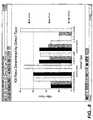
- Process flow in accordance with conventional memory bitmap testingis illustrated in Figure 1.
- a waferis subjected to both in-line inspection (right-hand column) and end-of-line testing (left-hand column).
- In-line inspectionmay be performed, for example, using optical inspection equipment such as the KLA21xx series available from KLA Tencor.
- In-line inspectionsproduce defect files containing X, Y location optical defect information. This information may then be output in any convenient format, an example of which is a format used by the Yield Manager tool of the former assignee, Knights Technology.
- End-of-line testingis performed using a tester, sometimes referred to as ATE (Automatic Test Equipment). The tester identifies failed memory locations. This information is processed to identify X,Y defect locations.
- ATEAutomatic Test Equipment
- the X, Y defect informationmay also be output to the Yield Manager tool. Because in-line and end-of-line defect information is in the same format within the Yield Manager tool, a combined defect overlay may be obtained, enabling "killer defects" (defects that render a part non-functional) to be identified. In particular, if the locations of a defect and a failure coincide, the defect may be presumed to a be a killer defect, i.e., a direct cause of the failure, in which case trouble-shooting would then focus on the production process rather than the underlying design of the part.
- killer defectsdefects that render a part non-functional
- yield enhancement organizations within semiconductor manufacturing plants, or fabshave long relied on memory chips to de-bug a given generation of technology.
- Yield enhancement engineershave typically used a memory production line to monitor the production process and ensure yield on other production lines of logic products using the same technology.
- in-line defect inspection toolshave been used, together with end-of-line functional test bitmap results.
- Memory bitmap failure datamay be further summarized into failure categories (e.g., single-bit failure, column failure, row failure, etc.).
- failure analysis engineerscan use a variety of "physical deprocessing" methods to identify the root cause of the failure. Based on the failure category, engineers can estimate where in the production process the failure occurred (e.g., the polysilicon layer deposition step, the metal 1 layer deposition step, etc.).
- logic-only fabscannot take full advantage of yield enhancement techniques developed within the industry over many years.
- the logic-only yield enhancement engineer todayis severely handicapped when compared to counterparts in fabs that run memory products.
- bitmaparea of logic within a chip.
- logic chip functional test resultsdo not provide a starting point for the physical coordinates of failures within a failed die.
- Scan testingbreaks the logic real estate of a chip into many discrete chains of logic which can be tested individually for basic functionality. Scan testing enables a list of failing signals to be identified. However, even after a list of failing signals is produced for a given die, it is still not possible to find the physical location of the failure because each failing signal may contain hundreds of transistors within its "cone of logic,” and there are usually multiple failing signals.
- Traditional logic chip yield enhancement techniquestherefore rely heavily on correlation of binsort functional test results to anticipate and correct semiconductor process issues.
- This approachsuffers from several drawbacks, including: the inability to relate a particular bin's fallout to a suspect process level; the inability to distinguish pre-packaging yield issue from packaging yield issues; and the inability to establish a clear link between large populations of failed die.
- Failure analysismay make use of a known electrical diagnosis process whereby a diagnostic list of suspected failing nets may be obtained as shown in Figure 2.
- Packaged devices having BIST (scan) capabilitiesare tested using a tester.
- Scan failure datais translated into format that can be used by an ATPG (Automatic Test Pattern Generation) tool, e.g., an ATPG tool used previously to generate test pattern files used by the tester.
- ATPGAutomatic Test Pattern Generation
- the ATPG toolsuses the translated test data, together with the test pattern files, setup files, one or more ATPG diagnostic models, and design information from a design database in order to identify suspected failing nodes, output in the form of a diagnostic list ( Figure 3).
- CAD navigation toolshave been developed to aid in failure analysis.
- CAD navigationrefers to the ability to point and click within a circuit layout display and by so doing automatically drive a piece of equipment such as FIB (Focussed Ion Beam) equipment to that location on the chip.
- FIBFluorescence Ion Beam
- CAD navigationalso allows a user to specify the name of a net, causing the corresponding layout to be displayed.
- One such CAD navigation toolis the Merlin Framework CAD navigation tool of the former assignee Knights Technology. This tool takes netlist information, layout information, and cross-reference files relating the two and produces a unified database in a Knights-proprietary format having an efficient indexing structure. Referring more particularly to Figure 4, the process of creating such a Knights database is illustrated in greater detail.
- a SPICE-formatted netlistis converted (if required) to a suitable netlist format.
- Data from a Schematic Verification databaseis converted (if required) to obtain cross-reference files cross-referencing net names and numerical net identifiers.
- Layout datais converted (if required) to a suitable polygon layout format.
- An MMapper routineuses the netlist, cross-reference files and polygon layout files in the following manner to produce a database suitable for CAD navigation.
- US Patent 5475695discloses a method of generating a defect identification matrix for a logic circuit, and a method of using the defect identification matrix, together with circuit models, to identify defects in the logic circuit. Automatic testing equipment is used to execute end of line tests on the logic circuit according to the defect identification matrix and circuit models.
- the present inventiontakes advantage of the foregoing capability to determine and display the X, Y location corresponding to a net name, by translating functional test data of a digital logic chip passed through a simulation model which identifies one or more defective nets of the chip.
- the defective netsare processed against a database of the foregoing type to obtain X, Y co-ordinate data for these nets, allowing them to be data logged as physical traces on the chip layout.
- this mappingis performed by taking the output from a functional tester and translating it from a list of failed scan chains into a list of suspected netlist nodes.
- the X,Y co-ordinates of suspected netlist nodesare then identified and stored in a database, providing failure analysis and yield enhancement engineers a starting point for performing failure analysis and for immediately understanding whether "in-line" inspection data can account for a given failure.
- These nodesmay then be crossmapped from the circuit design onto the chip's layout for each of multiple photomask layers within the design.
- Detailed failure datais gathered and stored at the wafer stage as part of a comprehensive program rather than on an as-needed basis at the packaged part stage. A voluminous amount of high-quality data is therefore obtained in an entirely automated fashion, as opposed to obtaining a comparatively minuscule amount of lesser-quality data in an exceedingly laborious fashion.
- Logic Mapallows the X,Y coordinates of failing netlist nodes to be generated.
- a generalized representation of the flow of data in the Logic Map systemis shown in Figure 6.
- Logic Mapbegins with wafer-level functional testing, which produces a functional test output file (e.g., an ASCII file). Once a functional test output file has been obtained, known methods may be used to post-process the functional test results and convert them into a list of failed signals suitable for input into a design diagnostic model.
- Various commercial circuit analysis toolsprovide for design diagnostic modeling. One such tool is the FastScan circuit analysis tool of Mentor Graphics.
- the converted functional test output fileis input to a circuit analysis tool.
- the function of the circuit analysis toolis to produce a list of suspected failing nets. An example of such a list is shown in Figure 3.
- the precision with which the suspected netlist vectors identify failure locationsdepend on the adequacy of the design diagnostic model, or simulation model.
- the circuit designer's inputis needed to establish an accurate and efficient model of a design. In some cases it may be necessary to modify the circuit simulation in order to obtain a suitable balance between the number of suspected fail vectors and the time required for circuit analysis.
- simulation modelsare intended to use as much computing time as necessary to find the minimum number of suspected failed netlist nodes. For example, for a circuit designer to run a simulation model of one failed die make take several minutes to one hour to produce one or two suspected failure vectors. This manner of operation is consistent with the role the circuit analysis tool usually plays in circuit design and verification. To adapt the simulation model to translate functional test data within a production wafer fab, the output datastream of suspected netlist nodes is caused to be much higher than in the circuit design and verification role.
- the simulation model running in a production fabshould be able to diagnose a failed die within one minute, even if that means that the list of suspected failing nodes will be larger (e.g., 3 to 10 nodes).
- the simulation modelis adapted to run in batch mode, or background mode. Hands-off, continuous processing of test data and enterprise-wide, real-time distribution of results is thereby achieved.
- the output of the simulation modelis continuously directed to a translator for conversion to a standard defect file format.
- a suitable translatoris provided by the Merlin CAD navigation framework software of the former assignee, Knights Technology.
- the framework softwareconverts the output datastream of suspected failing nodes to a physical bitmap file using layout data for the wafer.
- the framework softwarealso allows the physical bitmap may be overlaid onto the device layout as a layout trace, as shown in Figure 7.
- the layout tracemay be displayed in as many dimensions as there are photomasks.
- each photomask level's trace of the suspect failing netlist nodesis output into a separate file so that precise correlations with in-line defect data can be made (i.e., metal defects can be compared to a suspected node ⁇ s fail trace at the metal photomask).
- the physical bitmap filemay be exported to various yield management tools such as the Yield Manager tool of the present assignee.
- Yield management toolsprovide various visualization options, e.g., defect wafermaps, bitmaps, and charts. Kill ratio charts, an example of which is shown in Figure 8, are available to evaluate the degree of detect matches to logic bitmap failures.
- Bitmap failure intensity stackmapsan example of which is shown in Figure 9, can suggest areas of the layout susceptible to failure.
- bitmap datamay be output into any of various standard output formats for detect data, e.g., KLA format, ESDA format, etc. In this manner, logic mapping data and in-line test data may be collected in a common format for further processing.
- FIG. 10An alternative representation of the Logic Map process is shown in Figure 10.
- Datalogs for each die testedare sent to a server (e.g., a Unix server running an ATPG software package such as Fastscan, Sunrise, etc.). If a chip experiences a fundamental failure, then the datalog obtained for that chip is not usable. Typically, however, a large fraction of the datalogs are usable.
- the servertranslates these datalogs into an appropriate simulation format.
- Logic Mapuses the translated datalogs and design data to generate the X, Y coordinates of failing netlist nodes.
- the design data used by the logic mappermay include, for example, input from GDSII layout files, netlist data, and LVS (Layout Versus Schematic) data.
- the X,Y coordinate datamay then be used for both failure analysis and yield analysis. Whereas failure analysis is usually a rather prolonged process, yield analysis has real-time data requirements.
- the Logic Map processsatisfies these real-time data requirements as described hereinafter.
- datalogs for each die testedare sent to a server (e.g., a Unix server running an ATPG software package such as Fastscan, Sunrise, etc.) where a fraction of the datalogs are translated into an appropriate simulation format.
- Logic Mapuses the translated datalogs and design data to generate the X, Y coordinates of failing netlist nodes. This information may be stored in a database of a yield management tool such as the Yield Manager tool of Knights Technology.
- the Logic Map translatorconverts incoming diagnostic lists into a standard defect data format.
- the resulting diagnostic datais combined with in-line inspection data within the Yield Manager database.
- the Yield Manager databaseis used to overlay in-line defect data and Logic Map data.
- client softwaresuch as the Yield Manager client, running on high-end (e.g., Windows NT) PCs, may be used to enable visualization of the data in various ways, e.g., wafermaps, charts, layout, etc.
- datamay be exported in various file formats to facilitate data sharing.
- Defect matchingmay be performed based on a user-defined proximity radius from defects (in-line) to any point on a Logic Mapper trace. Yield management tools can be used to pre-filter defect data to eliminate ônuisanceö defects prior to matching. Defects with product-correlated hits can be exported back to the CAD navigation framework, e.g., for FIB (Focussed Ion Beam) navigation and de-processing. The defects which are hits can be selectively analyzed as a group to determine what defect types are most likely to be fatal and to determine other important distinctions such as defect size or intensity distribution. There results a new paradigm of how to use test data.
- FIBFrocussed Ion Beam
- Figure 12The layout of Figure 12 is such that operations performed are represented in the center column and data (or program) inputs are represented in the left-hand and right-hand flanking columns.
- the upper portion of the figurerelates to electrical diagnostic flow. Note that, as compared to conventional electrical diagnostic flow ( Figure 2), in Figure 12, wafers are tested rather than packaged devices. A test program is modified in order to obtain detailed failure data rather than simple "go/no-go" data as in a conventional production line.
- a die decode table and a decode translatorare developed for each device type to ensure that test data associated with a particular die on a wafer is mapped to the correct die coordinates within the Yield Manager database.
- the lower portion of the figurerelates to the Logic Map process flow.
- Diagnostic datais translated into a format readable by a polygon file generator.
- the polygon file generatorreads the translated diagnostic data and processes it against the database previously obtained ( Figure 4) in order to generate polygon files. These polygon files may in turn be translated to obtain standard defect files of a desired format.
Landscapes
- Engineering & Computer Science (AREA)
- Computer Hardware Design (AREA)
- General Engineering & Computer Science (AREA)
- Physics & Mathematics (AREA)
- General Physics & Mathematics (AREA)
- Tests Of Electronic Circuits (AREA)
- Testing Or Measuring Of Semiconductors Or The Like (AREA)
- Test And Diagnosis Of Digital Computers (AREA)
- Semiconductor Integrated Circuits (AREA)
Abstract
Description
Claims (9)
- A method of automated defect localization in the testing of logicsemiconductor integrated circuits, comprising the steps of:testing the logic integrated circuits to obtain generalised failuredata;inputting the generalised failure data and circuit models describinglogical operations of the integrated circuits to a circuit analysis tool;obtaining from the circuit analysis tool first localised probabledefect data;performing in-line inspection of the integrated circuits to obtainsecond localised probable defect data; andcorrelating the first and second localised probable defect data.
- The method of Claim 1, wherein the steps of inputting thegeneralised failure data to a circuit analysis tool and obtaining from thecircuit analysis tool first localised probable defect data are performedcontinuously using at least one programmed computer.
- The method of Claim 1, wherein correlating the first and secondlocalised probable defect data comprises producing a visual overlay ofthe first and second localised probable defect data.
- The method of Claim 1, wherein the integrated circuits are logiccircuits having built-in self-test capabilities.
- The method of Claim 1, wherein the generalised failure data isobtained using end-of-line testing of the integrated circuits.
- The method of Claim 5, wherein the integrated circuits are tested inwafer form.
- The method of Claim 1, wherein obtaining from the circuit analysistool first localised probable defect data comprises:creating a database against which the logic defect data is processedto obtain physical defect data; andprocessing the logical defect data against the database to obtainphysical defect data.
- The method of Claim 7, wherein creating the database comprisestranslating design information from a first format to a second format.
- A system for testing logic semiconductor integrated circuits,comprising:means for obtaining generalised failure data from testing the logicintegrated circuits;means for inputting the generalised failure data and circuit modelsdescribing logical operations of the integrated circuits to a circuitanalysis tool;means for obtaining from the circuit analysis tool first localisedprobable defect data;means for obtaining second localised probable defect data fromin-line inspection of the integrated circuits; andmeans for correlating the first and second localised probable defectdata.
Applications Claiming Priority (3)
| Application Number | Priority Date | Filing Date | Title |
|---|---|---|---|
| US09/192,164US6185707B1 (en) | 1998-11-13 | 1998-11-13 | IC test software system for mapping logical functional test data of logic integrated circuits to physical representation |
| US192164 | 1998-11-13 | ||
| PCT/US1999/026735WO2000030119A1 (en) | 1998-11-13 | 1999-11-12 | Ic test software system for mapping logical functional test data of logic integrated circuits to physical representation |
Publications (3)
| Publication Number | Publication Date |
|---|---|
| EP1149385A1 EP1149385A1 (en) | 2001-10-31 |
| EP1149385A4 EP1149385A4 (en) | 2002-01-30 |
| EP1149385B1true EP1149385B1 (en) | 2005-03-16 |
Family
ID=22708519
Family Applications (1)
| Application Number | Title | Priority Date | Filing Date |
|---|---|---|---|
| EP99958909AExpired - LifetimeEP1149385B1 (en) | 1998-11-13 | 1999-11-12 | Ic test software system for mapping logical functional test data of logic integrated circuits to physical representation |
Country Status (9)
| Country | Link |
|---|---|
| US (1) | US6185707B1 (en) |
| EP (1) | EP1149385B1 (en) |
| JP (1) | JP2002530659A (en) |
| KR (1) | KR100527911B1 (en) |
| CN (1) | CN1256733C (en) |
| AT (1) | ATE291274T1 (en) |
| DE (1) | DE69924296T8 (en) |
| TW (1) | TW440859B (en) |
| WO (1) | WO2000030119A1 (en) |
Cited By (2)
| Publication number | Priority date | Publication date | Assignee | Title |
|---|---|---|---|---|
| CN105093092A (en)* | 2015-07-09 | 2015-11-25 | 无锡中微腾芯电子有限公司 | Excel adopted method to realize the Summary standardization in wafer test |
| CN115562617A (en)* | 2022-11-30 | 2023-01-03 | 苏州浪潮智能科技有限公司 | Depth setting method and system of FIFO memory and electronic equipment |
Families Citing this family (83)
| Publication number | Priority date | Publication date | Assignee | Title |
|---|---|---|---|---|
| JP3055516B2 (en)* | 1997-12-25 | 2000-06-26 | 日本電気株式会社 | Apparatus and method for inspecting and analyzing semiconductor integrated circuit, and recording medium recording control program therefor |
| US6618830B1 (en)* | 1998-11-30 | 2003-09-09 | Texas Instruments Incorporated | System and method for pruning a bridging diagnostic list |
| US6487511B1 (en)* | 1999-01-21 | 2002-11-26 | Advanced Micro Devices, Inc. | Method and apparatus for measuring cumulative defects |
| JP3267580B2 (en)* | 1999-04-14 | 2002-03-18 | 日本電気株式会社 | Data processing method and apparatus, information storage medium |
| US6553329B2 (en)* | 1999-12-13 | 2003-04-22 | Texas Instruments Incorporated | System for mapping logical functional test data of logical integrated circuits to physical representation using pruned diagnostic list |
| US6745370B1 (en)* | 2000-07-14 | 2004-06-01 | Heuristics Physics Laboratories, Inc. | Method for selecting an optimal level of redundancy in the design of memories |
| US6601205B1 (en)* | 2000-09-29 | 2003-07-29 | Infineon Technologies Ag | Method to descramble the data mapping in memory circuits |
| TW533422B (en)* | 2000-11-28 | 2003-05-21 | Advantest Corp | Fail analysis device |
| US20020170028A1 (en)* | 2001-05-11 | 2002-11-14 | Liwei Chour | Computer-aided layout design system with automatic defect-zooming function |
| US6775796B2 (en) | 2001-08-31 | 2004-08-10 | International Business Machines Corporation | Creation of memory array bitmaps using logical to physical server |
| JP3904419B2 (en)* | 2001-09-13 | 2007-04-11 | 株式会社日立製作所 | Inspection device and inspection system |
| US7146584B2 (en)* | 2001-10-30 | 2006-12-05 | Teradyne, Inc. | Scan diagnosis system and method |
| WO2003098241A1 (en)* | 2002-05-14 | 2003-11-27 | Logicvision (Canada), Inc. | Method of and program product for performing gate-level diagnosis of failing vectors |
| US6842866B2 (en)* | 2002-10-25 | 2005-01-11 | Xin Song | Method and system for analyzing bitmap test data |
| AU2003302532A1 (en)* | 2002-11-19 | 2004-06-23 | Prophicy Semiconductor, Inc. | System and method for automated electronic device design |
| US7602510B2 (en)* | 2003-03-31 | 2009-10-13 | Eastman Kodak Company | Post RIP image rendering in an electrographic printer to reduce toner consumption |
| US20050039089A1 (en)* | 2003-08-11 | 2005-02-17 | Elias Gedamu | System and method for analysis of cache array test data |
| US7529988B1 (en)* | 2003-09-02 | 2009-05-05 | Advanced Micro Devices, Inc. | Storage of descriptive information in user defined fields of failure bitmaps in integrated circuit technology development |
| US7114143B2 (en)* | 2003-10-29 | 2006-09-26 | Lsi Logic Corporation | Process yield learning |
| US7653523B2 (en)* | 2003-12-15 | 2010-01-26 | Lsi Corporation | Method for calculating high-resolution wafer parameter profiles |
| JP2007528553A (en)* | 2004-03-09 | 2007-10-11 | セヤン ヤン | DYNAMIC VERIFICATION FOR IMPROVING VERIFICATION PERFORMANCE AND VERIFICATION EFFICIENCY-A verification method based on a basic method and a verification methodology using the same |
| CN1934831B (en)* | 2004-03-17 | 2010-09-29 | 皇家飞利浦电子股份有限公司 | Integrated circuit and method for communication service mapping |
| US7137085B1 (en)* | 2004-06-01 | 2006-11-14 | Advanced Micro Devices, Inc. | Wafer level global bitmap characterization in integrated circuit technology development |
| CN100413018C (en)* | 2004-06-14 | 2008-08-20 | 中芯国际集成电路制造(上海)有限公司 | Method and system for treating identity of semiconductor device |
| CN100428401C (en)* | 2004-06-14 | 2008-10-22 | 中芯国际集成电路制造(上海)有限公司 | Method and system for treating similarity of semiconductor device finished product ratio |
| US7013192B2 (en)* | 2004-06-14 | 2006-03-14 | Lsi Logic Corporation | Substrate contact analysis |
| US20060020442A1 (en)* | 2004-07-22 | 2006-01-26 | Elias Gedamu | Built-in self-test emulator |
| US20060020411A1 (en)* | 2004-07-22 | 2006-01-26 | Elias Gedamu | Built-in self-test emulator |
| US20060143524A1 (en)* | 2004-07-22 | 2006-06-29 | Elias Gedamu | Built-in self-test emulator |
| US20060031789A1 (en)* | 2004-07-22 | 2006-02-09 | Elias Gedamu | Built-in self-test emulator |
| US7194706B2 (en)* | 2004-07-27 | 2007-03-20 | International Business Machines Corporation | Designing scan chains with specific parameter sensitivities to identify process defects |
| US6998866B1 (en)* | 2004-07-27 | 2006-02-14 | International Business Machines Corporation | Circuit and method for monitoring defects |
| US7089514B2 (en)* | 2004-08-10 | 2006-08-08 | International Business Machines Corporation | Defect diagnosis for semiconductor integrated circuits |
| US7415378B2 (en)* | 2005-01-31 | 2008-08-19 | Texas Instruments Incorporated | Methods for analyzing critical defects in analog integrated circuits |
| US7257784B2 (en)* | 2005-03-24 | 2007-08-14 | Taiwan Semiconductor Manufacturing Co., Ltd. | Method for integrally checking chip and package substrate layouts for errors |
| US7320115B2 (en)* | 2005-07-12 | 2008-01-15 | Taiwan Semiconductor Manufacturing Co., Ltd. | Method for identifying a physical failure location on an integrated circuit |
| US20070061637A1 (en)* | 2005-09-12 | 2007-03-15 | Lsi Logic Corporation | Process for conducting high-speed bitmapping of memory cells during production |
| US7543198B2 (en)* | 2005-10-21 | 2009-06-02 | International Business Machines Corporation | Test data reporting and analyzing using data array and related data analysis |
| WO2007114930A2 (en)* | 2006-03-31 | 2007-10-11 | Teseda Corporation | Secure test-for-yield chip diagnostics management system and method |
| KR100827440B1 (en) | 2006-09-29 | 2008-05-06 | 삼성전자주식회사 | Failure analysis method and system of semiconductor integrated circuit device |
| US20080115029A1 (en)* | 2006-10-25 | 2008-05-15 | International Business Machines Corporation | iterative test generation and diagnostic method based on modeled and unmodeled faults |
| US7765444B2 (en) | 2006-11-06 | 2010-07-27 | Nec Electronics Corporation | Failure diagnosis for logic circuits |
| KR100809340B1 (en) | 2007-01-15 | 2008-03-07 | 삼성전자주식회사 | Failure analysis method and system of semiconductor integrated circuit device |
| US7653888B2 (en)* | 2007-04-25 | 2010-01-26 | International Business Machines Corporation | System for and method of integrating test structures into an integrated circuit |
| US20080319568A1 (en)* | 2007-06-22 | 2008-12-25 | International Business Machines Corporation | Method and system for creating array defect paretos using electrical overlay of bitfail maps, photo limited yield, yield, and auto pattern recognition code data |
| US8064682B2 (en)* | 2007-06-29 | 2011-11-22 | Intel Corporation | Defect analysis |
| US7761765B2 (en)* | 2007-07-27 | 2010-07-20 | Gm Global Technology Operations, Inc. | Automated root cause identification of logic controller failure |
| US7512933B1 (en) | 2008-01-27 | 2009-03-31 | International Business Machines Corporation | Method and system for associating logs and traces to test cases |
| US7890914B2 (en)* | 2008-02-01 | 2011-02-15 | Texas Instruments Incorporated | Layout data reduction for use with electronic design automation tools |
| CN101621016B (en)* | 2008-07-02 | 2011-10-05 | 中芯国际集成电路制造(上海)有限公司 | Method and system for detecting defects in manufacture of integrated circuit |
| JP4759597B2 (en)* | 2008-07-28 | 2011-08-31 | ルネサスエレクトロニクス株式会社 | Failure analysis method and failure analysis apparatus for semiconductor integrated circuit |
| JP2009081466A (en)* | 2008-12-26 | 2009-04-16 | Nec Electronics Corp | Fault diagnosis method for a plurality of logic circuits |
| US20100174957A1 (en)* | 2009-01-08 | 2010-07-08 | International Business Machines Corporation | Correlation and overlay of large design physical partitions and embedded macros to detect in-line defects |
| JP5583766B2 (en)* | 2009-07-01 | 2014-09-03 | ケーエルエー−テンカー・コーポレーション | Method, system, and computer-readable medium for monitoring time-varying defect classification performance |
| US8312413B2 (en) | 2010-01-22 | 2012-11-13 | International Business Machines Corporation | Navigating analytical tools using layout software |
| US8261216B2 (en)* | 2010-08-12 | 2012-09-04 | International Business Machines Corporation | Automated planning in physical synthesis |
| US8453088B2 (en) | 2010-09-27 | 2013-05-28 | Teseda Corporation | Suspect logical region synthesis and simulation using device design and test information |
| US8930782B2 (en)* | 2011-05-16 | 2015-01-06 | Mentor Graphics Corporation | Root cause distribution determination based on layout aware scan diagnosis results |
| US9939488B2 (en) | 2011-08-31 | 2018-04-10 | Teseda Corporation | Field triage of EOS failures in semiconductor devices |
| US8907697B2 (en) | 2011-08-31 | 2014-12-09 | Teseda Corporation | Electrical characterization for a semiconductor device pin |
| US8412991B2 (en) | 2011-09-02 | 2013-04-02 | Teseda Corporation | Scan chain fault diagnosis |
| TWI455223B (en)* | 2011-09-22 | 2014-10-01 | Orise Technology Co Ltd | Apparatus and method for testing the embedded memory of display panel driving integrated circuit |
| US9329235B2 (en)* | 2013-03-13 | 2016-05-03 | Synopsys, Inc. | Localizing fault flop in circuit by using modified test pattern |
| US9411014B2 (en) | 2013-03-22 | 2016-08-09 | Synopsys, Inc. | Reordering or removal of test patterns for detecting faults in integrated circuit |
| US9239897B2 (en) | 2013-04-03 | 2016-01-19 | Synopsys, Inc. | Hierarchical testing architecture using core circuit with pseudo-interfaces |
| US9417287B2 (en) | 2013-04-17 | 2016-08-16 | Synopsys, Inc. | Scheme for masking output of scan chains in test circuit |
| US9588179B2 (en) | 2013-06-12 | 2017-03-07 | Synopsys, Inc. | Scheme for masking output of scan chains in test circuit |
| WO2014204470A1 (en)* | 2013-06-20 | 2014-12-24 | Hewlett Packard Development Company, L.P. | Generating a fingerprint representing a response of an application to a simulation of a fault of an external service |
| US10067187B2 (en) | 2013-07-19 | 2018-09-04 | Synopsys, Inc. | Handling of undesirable distribution of unknown values in testing of circuit using automated test equipment |
| US9230050B1 (en) | 2014-09-11 | 2016-01-05 | The United States Of America, As Represented By The Secretary Of The Air Force | System and method for identifying electrical properties of integrate circuits |
| CN105652232B (en)* | 2015-12-30 | 2018-04-06 | 国家电网公司 | A kind of online abnormality diagnostic method of electric power meter based on stream process and system |
| US10247777B1 (en) | 2016-11-10 | 2019-04-02 | Teseda Corporation | Detecting and locating shoot-through timing failures in a semiconductor integrated circuit |
| US10191112B2 (en)* | 2016-11-18 | 2019-01-29 | Globalfoundries Inc. | Early development of a database of fail signatures for systematic defects in integrated circuit (IC) chips |
| CN107480561B (en)* | 2017-07-21 | 2023-08-04 | 天津大学 | Hardware Trojan horse detection method based on few-state node traversal |
| US10776543B2 (en) | 2018-06-25 | 2020-09-15 | International Business Machines Corporation | Automated region based optimization of chip manufacture |
| US11600505B2 (en)* | 2018-10-31 | 2023-03-07 | Taiwan Semiconductor Manufacturing Co., Ltd. | Systems and methods for systematic physical failure analysis (PFA) fault localization |
| CN111208407B (en)* | 2018-11-21 | 2022-05-31 | 上海春尚电子科技有限公司 | Auxiliary test system for digital integrated circuit chip |
| US11302412B2 (en)* | 2019-06-03 | 2022-04-12 | Advantest Corporation | Systems and methods for simulated device testing using a memory-based communication protocol |
| KR20220011211A (en)* | 2019-07-25 | 2022-01-27 | 미쓰비시덴키 가부시키가이샤 | Inspection device, inspection program stored in recording medium and inspection method |
| US11561256B2 (en)* | 2019-12-31 | 2023-01-24 | Synopsys, Inc. | Correlation between emission spots utilizing CAD data in combination with emission microscope images |
| CN112974289B (en)* | 2020-11-09 | 2023-04-28 | 重庆康佳光电技术研究院有限公司 | Sorting method, sorting apparatus, computer-readable storage medium, and electronic device |
| CN115267485B (en)* | 2022-06-14 | 2025-05-09 | 北京汤谷软件技术有限公司 | Chip protection circuit wiring test system and method |
| CN117054846A (en)* | 2023-06-30 | 2023-11-14 | 珠海妙存科技有限公司 | Visual test method, system and device for chip and storage medium |
Family Cites Families (21)
| Publication number | Priority date | Publication date | Assignee | Title |
|---|---|---|---|---|
| US3906163A (en)* | 1973-09-14 | 1975-09-16 | Gte Automatic Electric Lab Inc | Peripheral control unit for a communication switching system |
| US4242751A (en)* | 1978-08-28 | 1980-12-30 | Genrad, Inc. | Automatic fault-probing method and apparatus for checking electrical circuits and the like |
| US4222514A (en)* | 1978-11-30 | 1980-09-16 | Sperry Corporation | Digital tester |
| DE3110140A1 (en)* | 1981-03-16 | 1982-09-23 | Siemens AG, 1000 Berlin und 8000 München | DEVICE AND METHOD FOR A RAPID INTERNAL LOGIC CHECK ON INTEGRATED CIRCUITS |
| US4733176A (en)* | 1984-09-13 | 1988-03-22 | Siemens Aktiengesellschaft | Method and apparatus for locating defects in an electrical circuit with a light beam |
| US4801869A (en)* | 1987-04-27 | 1989-01-31 | International Business Machines Corporation | Semiconductor defect monitor for diagnosing processing-induced defects |
| JPH0244269A (en)* | 1988-08-04 | 1990-02-14 | Mitsubishi Electric Corp | LSI failure analysis method |
| US4967337A (en)* | 1988-10-11 | 1990-10-30 | Texas Instruments Incorporated | Automated diagnostic system |
| US5219765A (en)* | 1990-09-12 | 1993-06-15 | Hitachi, Ltd. | Method for manufacturing a semiconductor device including wafer aging, probe inspection, and feeding back the results of the inspection to the device fabrication process |
| US5475694A (en)* | 1993-01-19 | 1995-12-12 | The University Of British Columbia | Fuzzy multiple signature compaction scheme for built-in self-testing of large scale digital integrated circuits |
| US5475695A (en)* | 1993-03-19 | 1995-12-12 | Semiconductor Diagnosis & Test Corporation | Automatic failure analysis system |
| US5596587A (en)* | 1993-03-29 | 1997-01-21 | Teradyne, Inc. | Method and apparatus for preparing in-circuit test vectors |
| US5469443A (en)* | 1993-10-01 | 1995-11-21 | Hal Computer Systems, Inc. | Method and apparatus for testing random access memory |
| US5963881A (en)* | 1995-09-22 | 1999-10-05 | Texas Instruments Incorporated | Method and system for enhancing the identification of causes of variations in the performance of manufactured articles |
| US5668745A (en)* | 1995-10-20 | 1997-09-16 | Lsi Logic Corporation | Method and apparatus for testing of semiconductor devices |
| US5720031A (en)* | 1995-12-04 | 1998-02-17 | Micron Technology, Inc. | Method and apparatus for testing memory devices and displaying results of such tests |
| WO1997035337A1 (en)* | 1996-03-19 | 1997-09-25 | Hitachi, Ltd. | Process control system |
| US6091846A (en)* | 1996-05-31 | 2000-07-18 | Texas Instruments Incorporated | Method and system for anomaly detection |
| JP3699215B2 (en)* | 1996-09-20 | 2005-09-28 | 株式会社アドバンテスト | LSI failure analysis equipment |
| JP3808575B2 (en)* | 1997-01-14 | 2006-08-16 | 株式会社東芝 | Yield analysis method and apparatus |
| US5771243A (en)* | 1997-02-07 | 1998-06-23 | Etron Technology, Inc. | Method of identifying redundant test patterns |
- 1998
- 1998-11-13USUS09/192,164patent/US6185707B1/ennot_activeExpired - Lifetime
- 1999
- 1999-11-12JPJP2000583043Apatent/JP2002530659A/enactivePending
- 1999-11-12EPEP99958909Apatent/EP1149385B1/ennot_activeExpired - Lifetime
- 1999-11-12WOPCT/US1999/026735patent/WO2000030119A1/enactiveIP Right Grant
- 1999-11-12ATAT99958909Tpatent/ATE291274T1/ennot_activeIP Right Cessation
- 1999-11-12CNCNB998156078Apatent/CN1256733C/ennot_activeExpired - Fee Related
- 1999-11-12KRKR10-2001-7006060Apatent/KR100527911B1/ennot_activeExpired - Fee Related
- 1999-11-12DEDE69924296Tpatent/DE69924296T8/ennot_activeExpired - Fee Related
- 2000
- 2000-05-05TWTW088119776Apatent/TW440859B/ennot_activeIP Right Cessation
Cited By (4)
| Publication number | Priority date | Publication date | Assignee | Title |
|---|---|---|---|---|
| CN105093092A (en)* | 2015-07-09 | 2015-11-25 | 无锡中微腾芯电子有限公司 | Excel adopted method to realize the Summary standardization in wafer test |
| CN105093092B (en)* | 2015-07-09 | 2018-01-05 | 无锡中微腾芯电子有限公司 | The method that wafer sort Summary standardization is realized using Excel |
| CN115562617A (en)* | 2022-11-30 | 2023-01-03 | 苏州浪潮智能科技有限公司 | Depth setting method and system of FIFO memory and electronic equipment |
| CN115562617B (en)* | 2022-11-30 | 2023-03-03 | 苏州浪潮智能科技有限公司 | Depth setting method, system and electronic equipment of a FIFO memory |
Also Published As
| Publication number | Publication date |
|---|---|
| EP1149385A1 (en) | 2001-10-31 |
| EP1149385A4 (en) | 2002-01-30 |
| DE69924296T2 (en) | 2006-02-02 |
| DE69924296D1 (en) | 2005-04-21 |
| KR100527911B1 (en) | 2005-11-09 |
| KR20020008108A (en) | 2002-01-29 |
| US6185707B1 (en) | 2001-02-06 |
| JP2002530659A (en) | 2002-09-17 |
| ATE291274T1 (en) | 2005-04-15 |
| TW440859B (en) | 2001-06-16 |
| CN1256733C (en) | 2006-05-17 |
| CN1342318A (en) | 2002-03-27 |
| WO2000030119A1 (en) | 2000-05-25 |
| DE69924296T8 (en) | 2006-04-27 |
Similar Documents
| Publication | Publication Date | Title |
|---|---|---|
| EP1149385B1 (en) | Ic test software system for mapping logical functional test data of logic integrated circuits to physical representation | |
| US6553329B2 (en) | System for mapping logical functional test data of logical integrated circuits to physical representation using pruned diagnostic list | |
| US5475695A (en) | Automatic failure analysis system | |
| US6950771B1 (en) | Correlation of electrical test data with physical defect data | |
| CN100410953C (en) | Error location identification method and system combining pure logic and physical layout information | |
| US6842866B2 (en) | Method and system for analyzing bitmap test data | |
| US11669957B2 (en) | Semiconductor wafer measurement method and system | |
| US5570376A (en) | Method and apparatus for identifying faults within a system | |
| JP2000311930A (en) | Semiconductor inspection apparatus and method for specifying attribute of each die on wafer in the apparatus | |
| US20040230928A1 (en) | Apparatus connectable to a computer network for circuit design verification, computer implemented method for circuit design verification, and computer progam product for controlling a computer system so as to verify circuit designs | |
| US6775796B2 (en) | Creation of memory array bitmaps using logical to physical server | |
| JP3111931B2 (en) | Inspection result analyzer, analysis method, and recording medium recording analysis program | |
| KR20030051064A (en) | Method for measuring fail probability by only defect, method for measuring defect limited yield using classification the extracted defect pattern's parameter, and system for measuring fail probability by only defect and the defect limited yield | |
| JP4190748B2 (en) | CAD tool for semiconductor failure analysis and semiconductor failure analysis method | |
| Appello et al. | Understanding yield losses in logic circuits | |
| JP4131918B2 (en) | Failure analysis apparatus and failure analysis method for semiconductor integrated circuit | |
| US7500165B2 (en) | Systems and methods for controlling clock signals during scan testing integrated circuits | |
| CN111782695B (en) | MPW multi-product joint measurement data processing method, storage medium and computer equipment | |
| Bhattacherjee et al. | CAD Navigation Principles | |
| US20060230371A1 (en) | Alternative methodology for defect simulation and system | |
| Khare et al. | Rapid failure analysis using contamination-defect-fault (CDF) simulation | |
| US7634127B1 (en) | Efficient storage of fail data to aid in fault isolation | |
| US20060282726A1 (en) | Semiconductor device, and apparatus and method for supporting design of semiconductor device | |
| White et al. | Design for semiconductor manufacturing. Bibliography | |
| JP2008116332A (en) | Method for diagnosing failure of a plurality of logic circuit |
Legal Events
| Date | Code | Title | Description |
|---|---|---|---|
| PUAI | Public reference made under article 153(3) epc to a published international application that has entered the european phase | Free format text:ORIGINAL CODE: 0009012 | |
| 17P | Request for examination filed | Effective date:20010607 | |
| AK | Designated contracting states | Kind code of ref document:A1 Designated state(s):AT BE CH CY DE DK ES FI FR GB GR IE IT LI LU MC NL PT SE | |
| A4 | Supplementary search report drawn up and despatched | Effective date:20011217 | |
| AK | Designated contracting states | Kind code of ref document:A4 Designated state(s):AT BE CH CY DE DK ES FI FR GB GR IE IT LI LU MC NL PT SE | |
| RIC1 | Information provided on ipc code assigned before grant | Free format text:7G 11C 29/00 A, 7G 01R 31/28 B, 7G 01R 31/3183 B | |
| RAP1 | Party data changed (applicant data changed or rights of an application transferred) | Owner name:TEXAS INSTRUMENTS INCORPORATED Owner name:ELECTROGLAS, INC. | |
| 17Q | First examination report despatched | Effective date:20021025 | |
| GRAP | Despatch of communication of intention to grant a patent | Free format text:ORIGINAL CODE: EPIDOSNIGR1 | |
| GRAS | Grant fee paid | Free format text:ORIGINAL CODE: EPIDOSNIGR3 | |
| RAP1 | Party data changed (applicant data changed or rights of an application transferred) | Owner name:TEXAS INSTRUMENTS INCORPORATED Owner name:FEI COMPANY | |
| GRAA | (expected) grant | Free format text:ORIGINAL CODE: 0009210 | |
| AK | Designated contracting states | Kind code of ref document:B1 Designated state(s):AT BE CH CY DE DK ES FI FR GB GR IE IT LI LU MC NL PT SE | |
| PG25 | Lapsed in a contracting state [announced via postgrant information from national office to epo] | Ref country code:NL Free format text:LAPSE BECAUSE OF FAILURE TO SUBMIT A TRANSLATION OF THE DESCRIPTION OR TO PAY THE FEE WITHIN THE PRESCRIBED TIME-LIMIT Effective date:20050316 Ref country code:LI Free format text:LAPSE BECAUSE OF FAILURE TO SUBMIT A TRANSLATION OF THE DESCRIPTION OR TO PAY THE FEE WITHIN THE PRESCRIBED TIME-LIMIT Effective date:20050316 Ref country code:IT Free format text:LAPSE BECAUSE OF FAILURE TO SUBMIT A TRANSLATION OF THE DESCRIPTION OR TO PAY THE FEE WITHIN THE PRESCRIBED TIME-LIMIT;WARNING: LAPSES OF ITALIAN PATENTS WITH EFFECTIVE DATE BEFORE 2007 MAY HAVE OCCURRED AT ANY TIME BEFORE 2007. THE CORRECT EFFECTIVE DATE MAY BE DIFFERENT FROM THE ONE RECORDED. Effective date:20050316 Ref country code:FI Free format text:LAPSE BECAUSE OF FAILURE TO SUBMIT A TRANSLATION OF THE DESCRIPTION OR TO PAY THE FEE WITHIN THE PRESCRIBED TIME-LIMIT Effective date:20050316 Ref country code:CH Free format text:LAPSE BECAUSE OF FAILURE TO SUBMIT A TRANSLATION OF THE DESCRIPTION OR TO PAY THE FEE WITHIN THE PRESCRIBED TIME-LIMIT Effective date:20050316 Ref country code:BE Free format text:LAPSE BECAUSE OF FAILURE TO SUBMIT A TRANSLATION OF THE DESCRIPTION OR TO PAY THE FEE WITHIN THE PRESCRIBED TIME-LIMIT Effective date:20050316 Ref country code:AT Free format text:LAPSE BECAUSE OF FAILURE TO SUBMIT A TRANSLATION OF THE DESCRIPTION OR TO PAY THE FEE WITHIN THE PRESCRIBED TIME-LIMIT Effective date:20050316 | |
| REG | Reference to a national code | Ref country code:GB Ref legal event code:FG4D | |
| REG | Reference to a national code | Ref country code:CH Ref legal event code:EP | |
| REG | Reference to a national code | Ref country code:IE Ref legal event code:FG4D | |
| REF | Corresponds to: | Ref document number:69924296 Country of ref document:DE Date of ref document:20050421 Kind code of ref document:P | |
| PG25 | Lapsed in a contracting state [announced via postgrant information from national office to epo] | Ref country code:GR Free format text:LAPSE BECAUSE OF FAILURE TO SUBMIT A TRANSLATION OF THE DESCRIPTION OR TO PAY THE FEE WITHIN THE PRESCRIBED TIME-LIMIT Effective date:20050616 Ref country code:DK Free format text:LAPSE BECAUSE OF FAILURE TO SUBMIT A TRANSLATION OF THE DESCRIPTION OR TO PAY THE FEE WITHIN THE PRESCRIBED TIME-LIMIT Effective date:20050616 | |
| PG25 | Lapsed in a contracting state [announced via postgrant information from national office to epo] | Ref country code:ES Free format text:LAPSE BECAUSE OF FAILURE TO SUBMIT A TRANSLATION OF THE DESCRIPTION OR TO PAY THE FEE WITHIN THE PRESCRIBED TIME-LIMIT Effective date:20050627 | |
| NLV1 | Nl: lapsed or annulled due to failure to fulfill the requirements of art. 29p and 29m of the patents act | ||
| PG25 | Lapsed in a contracting state [announced via postgrant information from national office to epo] | Ref country code:PT Free format text:LAPSE BECAUSE OF FAILURE TO SUBMIT A TRANSLATION OF THE DESCRIPTION OR TO PAY THE FEE WITHIN THE PRESCRIBED TIME-LIMIT Effective date:20050907 | |
| REG | Reference to a national code | Ref country code:CH Ref legal event code:PL | |
| PG25 | Lapsed in a contracting state [announced via postgrant information from national office to epo] | Ref country code:CY Free format text:LAPSE BECAUSE OF FAILURE TO SUBMIT A TRANSLATION OF THE DESCRIPTION OR TO PAY THE FEE WITHIN THE PRESCRIBED TIME-LIMIT Effective date:20051112 | |
| PG25 | Lapsed in a contracting state [announced via postgrant information from national office to epo] | Ref country code:IE Free format text:LAPSE BECAUSE OF NON-PAYMENT OF DUE FEES Effective date:20051114 | |
| PG25 | Lapsed in a contracting state [announced via postgrant information from national office to epo] | Ref country code:MC Free format text:LAPSE BECAUSE OF NON-PAYMENT OF DUE FEES Effective date:20051130 Ref country code:LU Free format text:LAPSE BECAUSE OF NON-PAYMENT OF DUE FEES Effective date:20051130 | |
| PLBE | No opposition filed within time limit | Free format text:ORIGINAL CODE: 0009261 | |
| STAA | Information on the status of an ep patent application or granted ep patent | Free format text:STATUS: NO OPPOSITION FILED WITHIN TIME LIMIT | |
| 26N | No opposition filed | Effective date:20051219 | |
| ET | Fr: translation filed | ||
| REG | Reference to a national code | Ref country code:IE Ref legal event code:MM4A | |
| REG | Reference to a national code | Ref country code:FR Ref legal event code:TQ | |
| PG25 | Lapsed in a contracting state [announced via postgrant information from national office to epo] | Ref country code:SE Free format text:LAPSE BECAUSE OF FAILURE TO SUBMIT A TRANSLATION OF THE DESCRIPTION OR TO PAY THE FEE WITHIN THE PRESCRIBED TIME-LIMIT Effective date:20050616 | |
| PGFP | Annual fee paid to national office [announced via postgrant information from national office to epo] | Ref country code:GB Payment date:20071107 Year of fee payment:9 Ref country code:FR Payment date:20071108 Year of fee payment:9 | |
| PGFP | Annual fee paid to national office [announced via postgrant information from national office to epo] | Ref country code:DE Payment date:20081223 Year of fee payment:10 | |
| GBPC | Gb: european patent ceased through non-payment of renewal fee | Effective date:20081112 | |
| REG | Reference to a national code | Ref country code:FR Ref legal event code:ST Effective date:20090731 | |
| PG25 | Lapsed in a contracting state [announced via postgrant information from national office to epo] | Ref country code:GB Free format text:LAPSE BECAUSE OF NON-PAYMENT OF DUE FEES Effective date:20081112 | |
| PG25 | Lapsed in a contracting state [announced via postgrant information from national office to epo] | Ref country code:DE Free format text:LAPSE BECAUSE OF NON-PAYMENT OF DUE FEES Effective date:20100601 | |
| PG25 | Lapsed in a contracting state [announced via postgrant information from national office to epo] | Ref country code:FR Free format text:LAPSE BECAUSE OF NON-PAYMENT OF DUE FEES Effective date:20081130 |