EP1133789B1 - Mechanical patterning of a device layer - Google Patents
Mechanical patterning of a device layerDownload PDFInfo
- Publication number
- EP1133789B1 EP1133789B1EP99933463AEP99933463AEP1133789B1EP 1133789 B1EP1133789 B1EP 1133789B1EP 99933463 AEP99933463 AEP 99933463AEP 99933463 AEP99933463 AEP 99933463AEP 1133789 B1EP1133789 B1EP 1133789B1
- Authority
- EP
- European Patent Office
- Prior art keywords
- substrate
- layer
- device layer
- stamp
- poly
- Prior art date
- Legal status (The legal status is an assumption and is not a legal conclusion. Google has not performed a legal analysis and makes no representation as to the accuracy of the status listed.)
- Expired - Lifetime
Links
- 238000000059patterningMethods0.000titleclaimsabstractdescription17
- 239000000758substrateSubstances0.000claimsabstractdescription59
- 238000004519manufacturing processMethods0.000claimsabstractdescription12
- 239000010410layerSubstances0.000claimsdescription63
- 238000000034methodMethods0.000claimsdescription38
- -1poly(ethylene terephthalate)Polymers0.000claimsdescription24
- 239000002346layers by functionSubstances0.000claimsdescription11
- 238000012545processingMethods0.000claimsdescription8
- 239000000463materialSubstances0.000claimsdescription6
- 229920000139polyethylene terephthalatePolymers0.000claimsdescription4
- 239000005020polyethylene terephthalateSubstances0.000claimsdescription4
- 239000004698PolyethyleneSubstances0.000claimsdescription3
- 239000004743PolypropyleneSubstances0.000claimsdescription3
- 229920003229poly(methyl methacrylate)Polymers0.000claimsdescription3
- 229920002492poly(sulfone)Polymers0.000claimsdescription3
- 229920001707polybutylene terephthalatePolymers0.000claimsdescription3
- 229920000573polyethylenePolymers0.000claimsdescription3
- 239000004926polymethyl methacrylateSubstances0.000claimsdescription3
- 229920001155polypropylenePolymers0.000claimsdescription3
- 229920000915polyvinyl chloridePolymers0.000claimsdescription3
- 239000004800polyvinyl chlorideSubstances0.000claimsdescription3
- 239000004642PolyimideSubstances0.000claimsdescription2
- 239000004793PolystyreneSubstances0.000claimsdescription2
- AMGQUBHHOARCQH-UHFFFAOYSA-Nindium;oxotinChemical compound[In].[Sn]=OAMGQUBHHOARCQH-UHFFFAOYSA-N0.000claimsdescription2
- 239000004417polycarbonateSubstances0.000claimsdescription2
- 229920000515polycarbonatePolymers0.000claimsdescription2
- 229920000728polyesterPolymers0.000claimsdescription2
- 229920001721polyimidePolymers0.000claimsdescription2
- 238000003825pressingMethods0.000claims2
- 229920002223polystyrenePolymers0.000claims1
- 238000005336crackingMethods0.000abstractdescription4
- 239000004033plasticSubstances0.000abstractdescription4
- 229920003023plasticPolymers0.000abstractdescription4
- 239000012044organic layerSubstances0.000description3
- XLOMVQKBTHCTTD-UHFFFAOYSA-NZinc monoxideChemical compound[Zn]=OXLOMVQKBTHCTTD-UHFFFAOYSA-N0.000description2
- 230000001413cellular effectEffects0.000description2
- 239000002800charge carrierSubstances0.000description2
- 238000005229chemical vapour depositionMethods0.000description2
- 238000000151depositionMethods0.000description2
- 238000000465mouldingMethods0.000description2
- 238000005240physical vapour depositionMethods0.000description2
- 238000000623plasma-assisted chemical vapour depositionMethods0.000description2
- 230000005855radiationEffects0.000description2
- 239000002094self assembled monolayerSubstances0.000description2
- 239000013545self-assembled monolayerSubstances0.000description2
- 229910000831SteelInorganic materials0.000description1
- 229910052782aluminiumInorganic materials0.000description1
- XAGFODPZIPBFFR-UHFFFAOYSA-NaluminiumChemical compound[Al]XAGFODPZIPBFFR-UHFFFAOYSA-N0.000description1
- 238000003491arrayMethods0.000description1
- 239000000919ceramicSubstances0.000description1
- 239000004020conductorSubstances0.000description1
- 229920000547conjugated polymerPolymers0.000description1
- 238000007796conventional methodMethods0.000description1
- 230000003247decreasing effectEffects0.000description1
- 238000013461designMethods0.000description1
- 238000011161developmentMethods0.000description1
- 239000003989dielectric materialSubstances0.000description1
- 239000010408filmSubstances0.000description1
- 239000011521glassSubstances0.000description1
- 229910052751metalInorganic materials0.000description1
- 239000002184metalSubstances0.000description1
- 229920000307polymer substratePolymers0.000description1
- 239000011347resinSubstances0.000description1
- 229920005989resinPolymers0.000description1
- 239000004065semiconductorSubstances0.000description1
- 229910052710siliconInorganic materials0.000description1
- 239000010703siliconSubstances0.000description1
- 238000004544sputter depositionMethods0.000description1
- 239000010959steelSubstances0.000description1
- 239000010409thin filmSubstances0.000description1
- TVIVIEFSHFOWTE-UHFFFAOYSA-Ktri(quinolin-8-yloxy)alumaneChemical compound[Al+3].C1=CN=C2C([O-])=CC=CC2=C1.C1=CN=C2C([O-])=CC=CC2=C1.C1=CN=C2C([O-])=CC=CC2=C1TVIVIEFSHFOWTE-UHFFFAOYSA-K0.000description1
- 238000009736wettingMethods0.000description1
- YVTHLONGBIQYBO-UHFFFAOYSA-Nzinc indium(3+) oxygen(2-)Chemical compound[O--].[Zn++].[In+3]YVTHLONGBIQYBO-UHFFFAOYSA-N0.000description1
- 229960001296zinc oxideDrugs0.000description1
- 239000011787zinc oxideSubstances0.000description1
Images


Classifications
- B—PERFORMING OPERATIONS; TRANSPORTING
- B81—MICROSTRUCTURAL TECHNOLOGY
- B81B—MICROSTRUCTURAL DEVICES OR SYSTEMS, e.g. MICROMECHANICAL DEVICES
- B81B7/00—Microstructural systems; Auxiliary parts of microstructural devices or systems
- B81B7/0006—Interconnects
- H—ELECTRICITY
- H10—SEMICONDUCTOR DEVICES; ELECTRIC SOLID-STATE DEVICES NOT OTHERWISE PROVIDED FOR
- H10K—ORGANIC ELECTRIC SOLID-STATE DEVICES
- H10K50/00—Organic light-emitting devices
- H10K50/80—Constructional details
- H10K50/805—Electrodes
- H10K50/81—Anodes
- H—ELECTRICITY
- H10—SEMICONDUCTOR DEVICES; ELECTRIC SOLID-STATE DEVICES NOT OTHERWISE PROVIDED FOR
- H10K—ORGANIC ELECTRIC SOLID-STATE DEVICES
- H10K71/00—Manufacture or treatment specially adapted for the organic devices covered by this subclass
- H10K71/621—Providing a shape to conductive layers, e.g. patterning or selective deposition
- B—PERFORMING OPERATIONS; TRANSPORTING
- B81—MICROSTRUCTURAL TECHNOLOGY
- B81C—PROCESSES OR APPARATUS SPECIALLY ADAPTED FOR THE MANUFACTURE OR TREATMENT OF MICROSTRUCTURAL DEVICES OR SYSTEMS
- B81C2201/00—Manufacture or treatment of microstructural devices or systems
- B81C2201/03—Processes for manufacturing substrate-free structures
- B81C2201/036—Hot embossing
- H—ELECTRICITY
- H10—SEMICONDUCTOR DEVICES; ELECTRIC SOLID-STATE DEVICES NOT OTHERWISE PROVIDED FOR
- H10K—ORGANIC ELECTRIC SOLID-STATE DEVICES
- H10K59/00—Integrated devices, or assemblies of multiple devices, comprising at least one organic light-emitting element covered by group H10K50/00
- H10K59/10—OLED displays
- H10K59/17—Passive-matrix OLED displays
- H—ELECTRICITY
- H10—SEMICONDUCTOR DEVICES; ELECTRIC SOLID-STATE DEVICES NOT OTHERWISE PROVIDED FOR
- H10K—ORGANIC ELECTRIC SOLID-STATE DEVICES
- H10K71/00—Manufacture or treatment specially adapted for the organic devices covered by this subclass
- H10K71/821—Patterning of a layer by embossing, e.g. stamping to form trenches in an insulating layer
Definitions
- the present inventionrelates to the fabrication of devices. More particularly, the invention relates to patterning of a device layer on a substrate.
- one or more device layersare formed on a substrate.
- the layersare sequentially deposited and patterned to create features on the surface of the substrate.
- the layerscan be patterned individually and/or as a combination of layers to form the desired features.
- the featuresserve as components that perform the desired functions, creating the device.
- LEDlight emitting diode
- an LED cell or pixelcomprises one or more functional layers sandwiched between two electrodes to form a functional stack. Charge carriers are injected from both electrodes. These charge carriers recombine in the functional layer or layers, causing visible radiation to emit.
- organic functional layersto form organic LEDs (OLEDs). Such devices are fabricated on rigid glass substrates having a thickness of about 0.3-1.1 mm.
- OLED devicescomprises a plurality of OLED pixels arranged to form a display, such as a flat panel display (FPD).
- a pixelated OLED deviceincludes, for example, a plurality of first electrode strips formed on the substrate. The strips are arranged in a first direction. One of more organic layers are formed on the first electrodes strips. A plurality of second electrode strips is formed over the organic layers in a second direction. Typically, the first and second electrode strips are orthogonal to each other. The intersections of the first and second electrode strips form LED pixels.
- the first electrode stripsare created on the substrate by patterning an electrode layer.
- the electrode layeris patterned by photolithographic and etch processes. For example, a photosensitive resist layer is deposited on the electrode. The resist layer is exposed with radiation having the desired pattern defined by a mask. After development, unwanted resist is removed to expose portions of the electrode beneath. The exposed portions are removed by a wet etch, leaving the desired pattern on the electrode layer.
- conventional techniques for patterning the electroderequire numerous steps, increasing raw process time and manufacturing cost.
- Document US 5,259,926discloses a method of manufacturing a thin-film pattern on a substrate wherein a mask layer is formed by molding an organic resin with a molding member.
- Document US 5,669,303discloses forming a predetermined pattern of a self-assembled monolayer by wetting a stamping surface having the predetermined pattern with a solution containing the self-assembled monolayer material and controllably contacting and removing the stamping surface from a substrate, so that the solution is transferred to the latter.
- the inventionrelates to patterning a device layer on a substrate during device fabrication.
- the patterning of the device layeris achieved using a stamp with a pattern thereon.
- the patternis formed by protrusions having a height greater than the thickness of the device layer to pattern the device layer.
- the stampis pressed against the surface of the substrate under a load which patterns the device layer.
- the loadis selected to precisely control cracking the edges of the patterned areas but without cracking the non-patterned areas.
- the inventionrelates generally to the fabrication of devices.
- the inventiondescribes a process for patterning a device layer on a substrate, particularly a device layer formed on a ductile or flexible substrate.
- Various types of devicescan be formed by the present invention. For example, electrical, mechanical, or electromechanical devices can be formed.
- the inventioncan be useful in fabricating a microelectromechanical system (MEMS).
- MEMSmicroelectromechanical system
- a process for forming a pixelated organic LED deviceis provided.
- Fig. 1shows a cross-section of an OLED pixel.
- a substrate 101is provided.
- the substrateprovides support for the LED pixel.
- a functional stack 105comprising of one or more organic functional layers 120 formed between conductive layers 110 and 150 is formed on the substrate, creating the LED pixel.
- the conductive layer 110serves as an anode and the conductive layer 150 serves as a cathode.
- a plurality of LED pixelscan be arranged on the substrate to form an FPD.
- the FPDis used in various consumer electronic products, including cellular phones, cellular smart phones, personal organizers, pagers, advertising panel, touch screen displays, teleconferencing equipment, multimedia equipment, virtual reality products, and display kiosks.
- Figs. 2-5show a process for patterning a device layer on a substrate in the fabrication of a device.
- the device fabricatedcomprises a pixelated OLED device. Forming other types of devices such as electrical and/or mechanical devices, including sensor arrays, is also useful.
- a substrate 201is provided on which the active components of the device are formed.
- the substratecomprises a plastic or a polymeric material.
- the substratecomprises a flexible substrate, such as poly(ethylene terephthalate) (PET) or polyester for forming flexible devices.
- PETpoly(ethylene terephthalate)
- the substratecan comprise a transparent substrate to serve as, for example, a display surface for an OLED display. The use of a flexible transparent substrate for forming a flexible display is also useful.
- plastic substratessuch as PET, poly(butylene terephthalate) (PBT), poly(ethylene naphthalate) (PEN), Polycarbonate (PC), polyimides (P1), polysulfones (PSO), and poly(p-phenylene ether sulfone) (PES) are useful.
- Other substratescomprising polyethylene (PE), polypropylene (PP), poly(vinyl chloride) (PVC), polystyrene (PS) and poly(methyl methacrylate) (PMMA), can also be used.
- the substrateshould be thin to result in a thin device while providing sufficient mechanical integrity during the fabrication process to support the active components.
- the substrateshould be as thin as possible while providing sufficient mechanical integrity during the fabrication process.
- the substrate thicknessis, for example, about 20 - 200 ⁇ m. Thicker substrates are also useful. For example, thicker substrate, can be used where device thickness or flexibility is not an issue.
- a device layer 210is formed on the substrate.
- the device layercomprises, for example, a conductive layer.
- the device layercomprises a transparent conductive layer that serves as an electrode for an LED device.
- the transparent conductive layercomprises an indium-tin-oxide (ITO). ITO is useful in forming the transparent anode of the LED device.
- ITOindium-tin-oxide
- Other transparent conductive layers, including zinc-oxide or indium-zinc-oxideare also useful.
- Various techniques, such as sputtering, physical vapor deposition (PVD), chemical vapor deposition (CVD) or plasma enhanced CVD (PECVD)can be employed to form the device layer.
- the device layeris deposited on the substrate to a thickness of about, for example, 100 nm. The thickness, of course, can vary depending on design requirements.
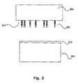
- a stamp 280comprising a desired pattern on a surface 231 is provided.
- the patternis defined by protrusions 285 on surface 231.
- the stampis made of a hard material such as steel, silicon, or ceramic. Other materials that are sufficiently hard can also be used to form the stamp.
- the patternis deeper than the thickness of the device layer. This ensures proper patterning of the device layer.
- the height of the protrusionsshould be less than that which would compromise the support function of the substrate.
- the height of the protrusionsis at least about 2 - 10 times the thickness of the device layer, preferably 5 - 10 times the thickness of the device layer.
- the height of the protrusionsis about 0.5 - 1 ⁇ m for a 100 nm thick device layer.
- the height of the protrusionscan be optimized according to the mechanical properties and thickness of the substrate.
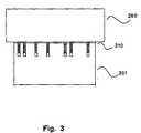
- a loadis applied on the stamp 280, forcing the stamp against the substrate 201. This causes the pattern on the stamp to be transferred to the substrate.
- the load applied on the stampis sufficient to prevent the device layer 210 from cracking in the active or non-patterned areas as it is patterned.
- the net pressure of the loadis about 200 - 400 MPa for a typical polymer substrate. In general, the required net pressure should exceed about 1.1 times the yield strength of the substrate material.
- the stampis lifted from the substrate. As shown, the pattern on the stamp is transferred onto the device layer. In one embodiment, the device layer is patterned to form electrode stripes on the substrate. Conventional processing continues to form the device.
- the processcontinues to fabricate OLED pixels of an OLED device. Fabrication of OLED pixels is described in, for example, United States Patent 4,720,432 and Burroughes et. al, Nature 347 (1990) 539 . This includes, for example, depositing one or more organic functional layers, such as conjugated polymer or Alq 3 , on the electrode. Other types of organic layers can also be useful. Preferably, a plurality of functional layers is formed on the electrode. Second electrode stripes comprising metal such as aluminum or other conductive material are formed over the functional layer. The second electrode stripes are typically orthogonal to the bottom electrode stripes. Providing second electrode stripes that are diagonal to the bottom electrode stripes is also useful. The intersections of the top and bottom electrode stripes form OLED pixels. Various techniques can be used to form the electrode stripes. For example, the second electrode stripes can be formed by selective deposition techniques. Alternatively, the electrode stripe can be formed by selectively patterning a top electrode layer to form the stripes.
- the pattern on the stampcan be formed to include a plurality of devices for parallel processing, thereby decreasing process time per device.
- the stamp patterncan be formed by a variety of techniques. Such techniques include, for example, grinding or photolithographic and etch processes.
- Fig. 5shows another embodiment of the invention.
- a stampcomprising a drum 580 with the desired pattern 585 thereon is provided.
- the drum stampis used in reel-to-reel processing.
- a long flexible substrate 501 with a device layer 510 formed thereonis provided.
- the substrateis translated through the drum while it is pressed under rotation, patterning the device layer.
- the substrateis translated in a direction from right to left and the drum stamp is rotated in the clockwise direction. Reversing the direction that the substrate is translated is also useful. Reel-to-reel processing enables parallel processing of devices.
Landscapes
- Engineering & Computer Science (AREA)
- Computer Hardware Design (AREA)
- Microelectronics & Electronic Packaging (AREA)
- Manufacturing & Machinery (AREA)
- Physics & Mathematics (AREA)
- Optics & Photonics (AREA)
- Electroluminescent Light Sources (AREA)
- Magnetic Heads (AREA)
- Surface Acoustic Wave Elements And Circuit Networks Thereof (AREA)
- Manufacturing Of Printed Wiring (AREA)
- Golf Clubs (AREA)
- Braking Arrangements (AREA)
- Laying Of Electric Cables Or Lines Outside (AREA)
Abstract
Description
- The present invention relates to the fabrication of devices. More particularly, the invention relates to patterning of a device layer on a substrate.
- In device fabrication, one or more device layers are formed on a substrate. The layers are sequentially deposited and patterned to create features on the surface of the substrate. The layers can be patterned individually and/or as a combination of layers to form the desired features. The features serve as components that perform the desired functions, creating the device.
- One type of device which is of particular interest is a light emitting diode (LED). Typically, an LED cell or pixel comprises one or more functional layers sandwiched between two electrodes to form a functional stack. Charge carriers are injected from both electrodes. These charge carriers recombine in the functional layer or layers, causing visible radiation to emit. Recently, significant advances have been made utilizing organic functional layers to form organic LEDs (OLEDs). Such devices are fabricated on rigid glass substrates having a thickness of about 0.3-1.1 mm.
- Typically, OLED devices comprises a plurality of OLED pixels arranged to form a display, such as a flat panel display (FPD). A pixelated OLED device includes, for example, a plurality of first electrode strips formed on the substrate. The strips are arranged in a first direction. One of more organic layers are formed on the first electrodes strips. A plurality of second electrode strips is formed over the organic layers in a second direction. Typically, the first and second electrode strips are orthogonal to each other. The intersections of the first and second electrode strips form LED pixels.
- The first electrode strips are created on the substrate by patterning an electrode layer. Conventionally, the electrode layer is patterned by photolithographic and etch processes. For example, a photosensitive resist layer is deposited on the electrode. The resist layer is exposed with radiation having the desired pattern defined by a mask. After development, unwanted resist is removed to expose portions of the electrode beneath. The exposed portions are removed by a wet etch, leaving the desired pattern on the electrode layer. Thus, conventional techniques for patterning the electrode require numerous steps, increasing raw process time and manufacturing cost.
- Document
US 5,259,926 discloses a method of manufacturing a thin-film pattern on a substrate wherein a mask layer is formed by molding an organic resin with a molding member. - Document
US 5,669,303 discloses forming a predetermined pattern of a self-assembled monolayer by wetting a stamping surface having the predetermined pattern with a solution containing the self-assembled monolayer material and controllably contacting and removing the stamping surface from a substrate, so that the solution is transferred to the latter. - InM. Berggren et al., "Organic solid-state lasers with imprinted gratings on plastic substrates" (Appl. Phys. Lett. 72 (1998), p. 410) a process for imprinting a distributed feedback resonator in the surface of a BCB layer is disclosed. In the process, a flexible substrate coated with a 4 µm thick BCB film is pressed against a mold with grooves which are 100 nm deep.
- As evidenced by the above discussion, it is desirable to provide a simplified process of patterning a device layer.
- The invention relates to patterning a device layer on a substrate during device fabrication. In accordance with the invention, the patterning of the device layer is achieved using a stamp with a pattern thereon. The pattern is formed by protrusions having a height greater than the thickness of the device layer to pattern the device layer. The stamp is pressed against the surface of the substrate under a load which patterns the device layer. The load is selected to precisely control cracking the edges of the patterned areas but without cracking the non-patterned areas.
Fig. 1 shows an organic pixel LED;Figs. 2-4 show a process for patterning a device layer in accordance with one embodiment of the invention; andFig. 5 shows an alternative process for patterning a device layer.- The invention relates generally to the fabrication of devices. In particular, the invention describes a process for patterning a device layer on a substrate, particularly a device layer formed on a ductile or flexible substrate. Various types of devices can be formed by the present invention. For example, electrical, mechanical, or electromechanical devices can be formed. Also, the invention can be useful in fabricating a microelectromechanical system (MEMS). In one embodiment, a process for forming a pixelated organic LED device is provided.
Fig. 1 shows a cross-section of an OLED pixel. As shown, asubstrate 101 is provided. The substrate provides support for the LED pixel. Afunctional stack 105 comprising of one or more organicfunctional layers 120 formed betweenconductive layers conductive layer 110 serves as an anode and theconductive layer 150 serves as a cathode.- A plurality of LED pixels can be arranged on the substrate to form an FPD. The FPD is used in various consumer electronic products, including cellular phones, cellular smart phones, personal organizers, pagers, advertising panel, touch screen displays, teleconferencing equipment, multimedia equipment, virtual reality products, and display kiosks.
Figs. 2-5 show a process for patterning a device layer on a substrate in the fabrication of a device. In one embodiment, the device fabricated comprises a pixelated OLED device. Forming other types of devices such as electrical and/or mechanical devices, including sensor arrays, is also useful.- Referring to
Fig. 2 , asubstrate 201 is provided on which the active components of the device are formed. The substrate comprises a plastic or a polymeric material. In one embodiment, the substrate comprises a flexible substrate, such as poly(ethylene terephthalate) (PET) or polyester for forming flexible devices. The substrate can comprise a transparent substrate to serve as, for example, a display surface for an OLED display. The use of a flexible transparent substrate for forming a flexible display is also useful. Various types of plastic substrates, such as PET, poly(butylene terephthalate) (PBT), poly(ethylene naphthalate) (PEN), Polycarbonate (PC), polyimides (P1), polysulfones (PSO), and poly(p-phenylene ether sulfone) (PES) are useful. Other substrates comprising polyethylene (PE), polypropylene (PP), poly(vinyl chloride) (PVC), polystyrene (PS) and poly(methyl methacrylate) (PMMA), can also be used. - In one embodiment, the substrate should be thin to result in a thin device while providing sufficient mechanical integrity during the fabrication process to support the active components. Preferably, the substrate should be as thin as possible while providing sufficient mechanical integrity during the fabrication process. The substrate thickness is, for example, about 20 - 200 µm. Thicker substrates are also useful. For example, thicker substrate, can be used where device thickness or flexibility is not an issue.
- A
device layer 210 is formed on the substrate. The device layer comprises, for example, a conductive layer. Other types of device layers, such as dielectrics or semiconductors, are also useful. In one embodiment the device layer comprises a transparent conductive layer that serves as an electrode for an LED device. The transparent conductive layer comprises an indium-tin-oxide (ITO). ITO is useful in forming the transparent anode of the LED device. Other transparent conductive layers, including zinc-oxide or indium-zinc-oxide are also useful. Various techniques, such as sputtering, physical vapor deposition (PVD), chemical vapor deposition (CVD) or plasma enhanced CVD (PECVD) can be employed to form the device layer. The device layer is deposited on the substrate to a thickness of about, for example, 100 nm. The thickness, of course, can vary depending on design requirements. - A
stamp 280 comprising a desired pattern on asurface 231 is provided. The pattern is defined byprotrusions 285 onsurface 231. The stamp is made of a hard material such as steel, silicon, or ceramic. Other materials that are sufficiently hard can also be used to form the stamp. - In the invention, the pattern is deeper than the thickness of the device layer. This ensures proper patterning of the device layer. However, the height of the protrusions should be less than that which would compromise the support function of the substrate. In one embodiment, the height of the protrusions is at least about 2 - 10 times the thickness of the device layer, preferably 5 - 10 times the thickness of the device layer. For example, the height of the protrusions is about 0.5 - 1 µm for a 100 nm thick device layer. The height of the protrusions can be optimized according to the mechanical properties and thickness of the substrate.
- Referring to
Fig. 3 , a load is applied on thestamp 280, forcing the stamp against thesubstrate 201. This causes the pattern on the stamp to be transferred to the substrate. The load applied on the stamp is sufficient to prevent thedevice layer 210 from cracking in the active or non-patterned areas as it is patterned. In one embodiment, the net pressure of the load is about 200 - 400 MPa for a typical polymer substrate. In general, the required net pressure should exceed about 1.1 times the yield strength of the substrate material. - Referring to
Fig. 4 , the stamp is lifted from the substrate. As shown, the pattern on the stamp is transferred onto the device layer. In one embodiment, the device layer is patterned to form electrode stripes on the substrate. Conventional processing continues to form the device. - In one embodiment, the process continues to fabricate OLED pixels of an OLED device. Fabrication of OLED pixels is described in, for example, United States Patent
4,720,432 andBurroughes et. al, Nature 347 (1990) 539. This includes, for example, depositing one or more organic functional layers, such as conjugated polymer or Alq3, on the electrode. Other types of organic layers can also be useful. Preferably, a plurality of functional layers is formed on the electrode. Second electrode stripes comprising metal such as aluminum or other conductive material are formed over the functional layer. The second electrode stripes are typically orthogonal to the bottom electrode stripes. Providing second electrode stripes that are diagonal to the bottom electrode stripes is also useful. The intersections of the top and bottom electrode stripes form OLED pixels. Various techniques can be used to form the electrode stripes. For example, the second electrode stripes can be formed by selective deposition techniques. Alternatively, the electrode stripe can be formed by selectively patterning a top electrode layer to form the stripes. - In an alternative embodiment, the pattern on the stamp can be formed to include a plurality of devices for parallel processing, thereby decreasing process time per device. The stamp pattern can be formed by a variety of techniques. Such techniques include, for example, grinding or photolithographic and etch processes.
Fig. 5 shows another embodiment of the invention. As shown, a stamp comprising adrum 580 with the desiredpattern 585 thereon is provided. The drum stamp is used in reel-to-reel processing. A long flexible substrate 501 with adevice layer 510 formed thereon is provided. The substrate is translated through the drum while it is pressed under rotation, patterning the device layer. As shown, the substrate is translated in a direction from right to left and the drum stamp is rotated in the clockwise direction. Reversing the direction that the substrate is translated is also useful. Reel-to-reel processing enables parallel processing of devices.
Claims (19)
- A method for the fabrication of a device comprising:providing a substrate (201, 501) comprising a device layer (210, 510) on its surface; andpatterning the device layer by pressing a stamp (280, 580) comprising a pattern against the device layer,characterized in that
the pattern comprises protrusions (285, 585) on a surface (231) of the stamp and the protrusions comprise a height greater than a thickness of the device layer. - The method of claim 1 wherein the device comprises an organic LED device.
- The method of one of claims 1 or 2 wherein the substrate (201, 501) comprises a polymeric substrate.
- The method of one of claims 1 to 3 wherein the substrate (201, 501) comprises a flexible or ductile substrate.
- The method of one of claims 1 to 4 wherein the substrate (201, 501) comprises a transparent substrate.
- The method of one of claims 1 to 5 wherein the device layer (210, 510) comprises a conductive layer.
- The method of claim 6 wherein the device comprises an organic LED device, and wherein the device layer (210, 510) comprises a transparent conductive layer.
- The method of claim 7 wherein the transparent conductive layer comprises a conductive oxide.
- The method of claim 8 wherein the conductive oxide comprises indium-tin-oxide.
- The method of one of claims 6 to 9 wherein patterning the device layer (210, 510) forms lower electrodes on the substrate.
- The method of one of the preceding claims wherein the height of the protrusions (285, 585) is 2 - 10 times greater than the thickness of the device layer (210).
- The method of claim 11 Wherein the height of the protrusions (285, 585) is 5-10 times greater than the thickness of the device layer (210, 510).
- The method of one of the preceding claims wherein the stamp (280, 580) is pressed against the device layer surface under a load which comprises a net pressure of greater than 1.10 times a yield strength of the substrate(201, 501).
- The method of one of the preceding claims further comprises processing to form OLED pixels.
- The method of claims 10 and 14 wherein the processing to form OLED pixels comprises:forming at least one organic functional layer (120) on lower electrodes (110); andforming upper electrodes (150) on the organicfunctional layer, wherein OLED pixels are formed where upper and lower electrodes sandwich the organic functional layer.
- The method of one of the preceding claims wherein the substrate (201, 501) comprises a material selected from the group consisting of polyester, poly(ethylene terephthalate), poly(butylene terephthalate), poly(ethylene naphthalate), polyethylenesterephtalate, polycarbonate, polyimides, polysulfones, poly(p-phenylene ether sulfone), polyethylene, polypropylene, poly(vinyl chloride), polystyrene, and poly(methyl methacrylate)
- The method of one of the preceding claims further comprises processing to form the device.
- The method of one of the preceding claims wherein the device comprises a device selected from the group consisting of an electrical device, a mechanical device, an electromechanical device, and a microelectromechanical system.
- The method of one of the preceding claims, wherein the stamp (580) comprises a drum with a pattern and pressing the stamp against the device layer (510) includes rotating the stamp comprising a drum with a pattern; and translating the substrate with the device layer thereon as the stamp is rotated to pattern the device layer.
Applications Claiming Priority (1)
| Application Number | Priority Date | Filing Date | Title |
|---|---|---|---|
| PCT/SG1999/000074WO2001004938A1 (en) | 1999-07-09 | 1999-07-09 | Mechanical patterning of a device layer |
Publications (2)
| Publication Number | Publication Date |
|---|---|
| EP1133789A1 EP1133789A1 (en) | 2001-09-19 |
| EP1133789B1true EP1133789B1 (en) | 2008-11-05 |
Family
ID=20430227
Family Applications (1)
| Application Number | Title | Priority Date | Filing Date |
|---|---|---|---|
| EP99933463AExpired - LifetimeEP1133789B1 (en) | 1999-07-09 | 1999-07-09 | Mechanical patterning of a device layer |
Country Status (11)
| Country | Link |
|---|---|
| US (1) | US6797211B1 (en) |
| EP (1) | EP1133789B1 (en) |
| JP (1) | JP2003504821A (en) |
| KR (1) | KR20010106470A (en) |
| CN (1) | CN1191609C (en) |
| AT (1) | ATE413362T1 (en) |
| AU (1) | AU4951399A (en) |
| CA (1) | CA2343227A1 (en) |
| DE (1) | DE69939877D1 (en) |
| TW (1) | TW529182B (en) |
| WO (1) | WO2001004938A1 (en) |
Families Citing this family (19)
| Publication number | Priority date | Publication date | Assignee | Title |
|---|---|---|---|---|
| ATE442765T1 (en) | 1999-07-09 | 2009-09-15 | Inst Materials Research & Eng | LAMINATES FOR ENCAPSULATING OLED DEVICES |
| KR20010106471A (en) | 1999-07-09 | 2001-11-29 | 추후보정 | Encapsulation of a device |
| WO2001044866A1 (en) | 1999-12-17 | 2001-06-21 | Osram Opto Semiconductors Gmbh | Improved organic led device |
| US7394153B2 (en) | 1999-12-17 | 2008-07-01 | Osram Opto Semiconductors Gmbh | Encapsulation of electronic devices |
| WO2001045140A2 (en) | 1999-12-17 | 2001-06-21 | Osram Opto Semiconductors Gmbh | Encapsulation for organic led device |
| JP2003517709A (en) | 1999-12-17 | 2003-05-27 | オスラム オプト セミコンダクターズ ゲゼルシャフト ミット ベシュレンクテル ハフツング | Improved encapsulation for organic light emitting diode devices |
| US6987613B2 (en)* | 2001-03-30 | 2006-01-17 | Lumileds Lighting U.S., Llc | Forming an optical element on the surface of a light emitting device for improved light extraction |
| US6936856B2 (en) | 2002-01-15 | 2005-08-30 | Osram Opto Semiconductors Gmbh | Multi substrate organic light emitting devices |
| KR100827617B1 (en)* | 2002-02-22 | 2008-05-07 | 엘지디스플레이 주식회사 | Organic light emitting device manufacturing method and polymer organic film pattern formation method thereof |
| KR100537722B1 (en)* | 2002-10-11 | 2005-12-20 | 강신일 | Method and device for ultraviolet continuous curing method for fabrication of micro patterns using drum-type stamper |
| FR2851346B1 (en)* | 2003-02-13 | 2005-07-01 | Gabriel Pascal Joseph Simon | INTERACTIVE SCREEN FOR ACQUIRING AND RETRIEVING GRAPHIC INFORMATION MANUALLY ENTERED |
| DE10330456B9 (en)* | 2003-07-05 | 2007-11-08 | Erich Thallner | Device for creating a surface structure on a wafer |
| US7524920B2 (en) | 2004-12-16 | 2009-04-28 | Eastman Chemical Company | Biaxially oriented copolyester film and laminates thereof |
| GB0523163D0 (en)* | 2005-11-14 | 2005-12-21 | Suisse Electronique Microtech | Patterning of conductive layers with underlying compressible spacer layer or spacer layer stack |
| GB2432721B (en)* | 2005-11-25 | 2011-06-22 | Seiko Epson Corp | Electrochemical cell structure and method of fabrication |
| GB2432722A (en)* | 2005-11-25 | 2007-05-30 | Seiko Epson Corp | Electrochemical cell and method of manufacture |
| GB2432723B (en)* | 2005-11-25 | 2010-12-08 | Seiko Epson Corp | Electrochemical cell and method of manufacture |
| US7667383B2 (en) | 2006-02-15 | 2010-02-23 | Osram Opto Semiconductors Gmbh | Light source comprising a common substrate, a first led device and a second led device |
| KR101534848B1 (en) | 2008-07-21 | 2015-07-27 | 엘지이노텍 주식회사 | Light emitting diodes and methods of making same. And a method for manufacturing the same |
Family Cites Families (5)
| Publication number | Priority date | Publication date | Assignee | Title |
|---|---|---|---|---|
| US4720432A (en) | 1987-02-11 | 1988-01-19 | Eastman Kodak Company | Electroluminescent device with organic luminescent medium |
| JPH0580530A (en) | 1991-09-24 | 1993-04-02 | Hitachi Ltd | Production of thin film pattern |
| JP3372258B2 (en) | 1995-08-04 | 2003-01-27 | インターナシヨナル・ビジネス・マシーンズ・コーポレーシヨン | Stamps for lithography processes |
| US5669303A (en) | 1996-03-04 | 1997-09-23 | Motorola | Apparatus and method for stamping a surface |
| JP3942715B2 (en)* | 1998-01-06 | 2007-07-11 | パイオニア株式会社 | Organic EL display panel and manufacturing method thereof |
- 1999
- 1999-07-09EPEP99933463Apatent/EP1133789B1/ennot_activeExpired - Lifetime
- 1999-07-09KRKR1020017003069Apatent/KR20010106470A/ennot_activeWithdrawn
- 1999-07-09CACA002343227Apatent/CA2343227A1/ennot_activeAbandoned
- 1999-07-09WOPCT/SG1999/000074patent/WO2001004938A1/ennot_activeApplication Discontinuation
- 1999-07-09USUS09/786,832patent/US6797211B1/ennot_activeExpired - Lifetime
- 1999-07-09CNCNB998106216Apatent/CN1191609C/ennot_activeExpired - Fee Related
- 1999-07-09ATAT99933463Tpatent/ATE413362T1/ennot_activeIP Right Cessation
- 1999-07-09AUAU49513/99Apatent/AU4951399A/ennot_activeAbandoned
- 1999-07-09JPJP2001509072Apatent/JP2003504821A/enactivePending
- 1999-07-09DEDE69939877Tpatent/DE69939877D1/ennot_activeExpired - Lifetime
- 2000
- 2000-07-07TWTW089113559Apatent/TW529182B/ennot_activeIP Right Cessation
Non-Patent Citations (1)
| Title |
|---|
| BERGGREN M. ET AL: "Organic solid state lasers with imprinted gratings on plastic substrates", APPLIED PHYSICS LETTERS, vol. 72, no. 4, 26 January 1998 (1998-01-26), AIP, USA, pages 410 - 412* |
Also Published As
| Publication number | Publication date |
|---|---|
| US6797211B1 (en) | 2004-09-28 |
| AU4951399A (en) | 2001-01-30 |
| CN1317148A (en) | 2001-10-10 |
| ATE413362T1 (en) | 2008-11-15 |
| TW529182B (en) | 2003-04-21 |
| KR20010106470A (en) | 2001-11-29 |
| WO2001004938A1 (en) | 2001-01-18 |
| CN1191609C (en) | 2005-03-02 |
| EP1133789A1 (en) | 2001-09-19 |
| JP2003504821A (en) | 2003-02-04 |
| DE69939877D1 (en) | 2008-12-18 |
| CA2343227A1 (en) | 2001-01-18 |
Similar Documents
| Publication | Publication Date | Title |
|---|---|---|
| EP1133789B1 (en) | Mechanical patterning of a device layer | |
| US7049630B2 (en) | Electrode patterning in OLED devices | |
| EP1573831B1 (en) | Methods of fabricating devices by low pressure cold welding | |
| EP1119878B1 (en) | Encapsulation of a device | |
| US7057337B1 (en) | Patterning of electrodes in OLED devices | |
| US9282648B2 (en) | Composite electrode and method of manufacture thereof | |
| US7737631B2 (en) | Flat panel display with repellant and border areas and method of manufacturing the same | |
| EP3333922B1 (en) | Organic luminescence unit and manufacturing method therefor | |
| US9446571B2 (en) | Touch panel and method of manufacturing touch panel | |
| US20030214232A1 (en) | Uniform deposition of organic layer | |
| WO2021108277A2 (en) | Stretchable polymer and dielectric layers for electronic displays | |
| CN1638545B (en) | Organic electroluminescent display device and manufacturing method thereof | |
| KR20180126108A (en) | Flexible display device and method of manufacturing for the same | |
| WO2003001490A2 (en) | Hybrid display device | |
| KR20060128232A (en) | Manufacturing method of organic light emitting diode display device |
Legal Events
| Date | Code | Title | Description |
|---|---|---|---|
| PUAI | Public reference made under article 153(3) epc to a published international application that has entered the european phase | Free format text:ORIGINAL CODE: 0009012 | |
| 17P | Request for examination filed | Effective date:20010409 | |
| AK | Designated contracting states | Kind code of ref document:A1 Designated state(s):AT BE CH CY DE DK ES FI FR GB GR IE IT LI LU MC NL PT SE | |
| 17Q | First examination report despatched | Effective date:20060914 | |
| GRAP | Despatch of communication of intention to grant a patent | Free format text:ORIGINAL CODE: EPIDOSNIGR1 | |
| RIC1 | Information provided on ipc code assigned before grant | Ipc:H01L 51/56 20060101ALI20080228BHEP Ipc:B81B 1/00 20060101AFI20080228BHEP | |
| GRAS | Grant fee paid | Free format text:ORIGINAL CODE: EPIDOSNIGR3 | |
| GRAA | (expected) grant | Free format text:ORIGINAL CODE: 0009210 | |
| AK | Designated contracting states | Kind code of ref document:B1 Designated state(s):AT BE CH CY DE DK ES FI FR GB GR IE IT LI LU MC NL PT SE | |
| REG | Reference to a national code | Ref country code:GB Ref legal event code:FG4D | |
| REG | Reference to a national code | Ref country code:CH Ref legal event code:EP | |
| REG | Reference to a national code | Ref country code:IE Ref legal event code:FG4D | |
| REF | Corresponds to: | Ref document number:69939877 Country of ref document:DE Date of ref document:20081218 Kind code of ref document:P | |
| NLV1 | Nl: lapsed or annulled due to failure to fulfill the requirements of art. 29p and 29m of the patents act | ||
| PG25 | Lapsed in a contracting state [announced via postgrant information from national office to epo] | Ref country code:ES Free format text:LAPSE BECAUSE OF FAILURE TO SUBMIT A TRANSLATION OF THE DESCRIPTION OR TO PAY THE FEE WITHIN THE PRESCRIBED TIME-LIMIT Effective date:20090216 Ref country code:AT Free format text:LAPSE BECAUSE OF FAILURE TO SUBMIT A TRANSLATION OF THE DESCRIPTION OR TO PAY THE FEE WITHIN THE PRESCRIBED TIME-LIMIT Effective date:20081105 | |
| PG25 | Lapsed in a contracting state [announced via postgrant information from national office to epo] | Ref country code:NL Free format text:LAPSE BECAUSE OF FAILURE TO SUBMIT A TRANSLATION OF THE DESCRIPTION OR TO PAY THE FEE WITHIN THE PRESCRIBED TIME-LIMIT Effective date:20081105 Ref country code:FI Free format text:LAPSE BECAUSE OF FAILURE TO SUBMIT A TRANSLATION OF THE DESCRIPTION OR TO PAY THE FEE WITHIN THE PRESCRIBED TIME-LIMIT Effective date:20081105 | |
| PG25 | Lapsed in a contracting state [announced via postgrant information from national office to epo] | Ref country code:DK Free format text:LAPSE BECAUSE OF FAILURE TO SUBMIT A TRANSLATION OF THE DESCRIPTION OR TO PAY THE FEE WITHIN THE PRESCRIBED TIME-LIMIT Effective date:20081105 Ref country code:BE Free format text:LAPSE BECAUSE OF FAILURE TO SUBMIT A TRANSLATION OF THE DESCRIPTION OR TO PAY THE FEE WITHIN THE PRESCRIBED TIME-LIMIT Effective date:20081105 | |
| PG25 | Lapsed in a contracting state [announced via postgrant information from national office to epo] | Ref country code:SE Free format text:LAPSE BECAUSE OF FAILURE TO SUBMIT A TRANSLATION OF THE DESCRIPTION OR TO PAY THE FEE WITHIN THE PRESCRIBED TIME-LIMIT Effective date:20090205 Ref country code:PT Free format text:LAPSE BECAUSE OF FAILURE TO SUBMIT A TRANSLATION OF THE DESCRIPTION OR TO PAY THE FEE WITHIN THE PRESCRIBED TIME-LIMIT Effective date:20090406 | |
| PLBE | No opposition filed within time limit | Free format text:ORIGINAL CODE: 0009261 | |
| STAA | Information on the status of an ep patent application or granted ep patent | Free format text:STATUS: NO OPPOSITION FILED WITHIN TIME LIMIT | |
| 26N | No opposition filed | Effective date:20090806 | |
| PG25 | Lapsed in a contracting state [announced via postgrant information from national office to epo] | Ref country code:MC Free format text:LAPSE BECAUSE OF NON-PAYMENT OF DUE FEES Effective date:20090731 | |
| REG | Reference to a national code | Ref country code:CH Ref legal event code:PL | |
| GBPC | Gb: european patent ceased through non-payment of renewal fee | Effective date:20090709 | |
| REG | Reference to a national code | Ref country code:FR Ref legal event code:ST Effective date:20100331 | |
| REG | Reference to a national code | Ref country code:IE Ref legal event code:MM4A | |
| PG25 | Lapsed in a contracting state [announced via postgrant information from national office to epo] | Ref country code:LI Free format text:LAPSE BECAUSE OF NON-PAYMENT OF DUE FEES Effective date:20090731 Ref country code:FR Free format text:LAPSE BECAUSE OF NON-PAYMENT OF DUE FEES Effective date:20090731 Ref country code:CH Free format text:LAPSE BECAUSE OF NON-PAYMENT OF DUE FEES Effective date:20090731 | |
| PG25 | Lapsed in a contracting state [announced via postgrant information from national office to epo] | Ref country code:GB Free format text:LAPSE BECAUSE OF NON-PAYMENT OF DUE FEES Effective date:20090709 | |
| PG25 | Lapsed in a contracting state [announced via postgrant information from national office to epo] | Ref country code:IE Free format text:LAPSE BECAUSE OF NON-PAYMENT OF DUE FEES Effective date:20090709 | |
| PG25 | Lapsed in a contracting state [announced via postgrant information from national office to epo] | Ref country code:GR Free format text:LAPSE BECAUSE OF FAILURE TO SUBMIT A TRANSLATION OF THE DESCRIPTION OR TO PAY THE FEE WITHIN THE PRESCRIBED TIME-LIMIT Effective date:20090206 | |
| PG25 | Lapsed in a contracting state [announced via postgrant information from national office to epo] | Ref country code:IT Free format text:LAPSE BECAUSE OF FAILURE TO SUBMIT A TRANSLATION OF THE DESCRIPTION OR TO PAY THE FEE WITHIN THE PRESCRIBED TIME-LIMIT Effective date:20081105 | |
| PG25 | Lapsed in a contracting state [announced via postgrant information from national office to epo] | Ref country code:LU Free format text:LAPSE BECAUSE OF NON-PAYMENT OF DUE FEES Effective date:20090709 | |
| PG25 | Lapsed in a contracting state [announced via postgrant information from national office to epo] | Ref country code:CY Free format text:LAPSE BECAUSE OF FAILURE TO SUBMIT A TRANSLATION OF THE DESCRIPTION OR TO PAY THE FEE WITHIN THE PRESCRIBED TIME-LIMIT Effective date:20081105 | |
| PGFP | Annual fee paid to national office [announced via postgrant information from national office to epo] | Ref country code:DE Payment date:20170727 Year of fee payment:19 | |
| REG | Reference to a national code | Ref country code:DE Ref legal event code:R119 Ref document number:69939877 Country of ref document:DE | |
| PG25 | Lapsed in a contracting state [announced via postgrant information from national office to epo] | Ref country code:DE Free format text:LAPSE BECAUSE OF NON-PAYMENT OF DUE FEES Effective date:20190201 |