EP1122577B1 - Spatial light modulator with conformal grating device - Google Patents
Spatial light modulator with conformal grating deviceDownload PDFInfo
- Publication number
- EP1122577B1 EP1122577B1EP01200128AEP01200128AEP1122577B1EP 1122577 B1EP1122577 B1EP 1122577B1EP 01200128 AEP01200128 AEP 01200128AEP 01200128 AEP01200128 AEP 01200128AEP 1122577 B1EP1122577 B1EP 1122577B1
- Authority
- EP
- European Patent Office
- Prior art keywords
- elongated element
- grating device
- mechanical grating
- mechanical
- intermediate support
- Prior art date
- Legal status (The legal status is an assumption and is not a legal conclusion. Google has not performed a legal analysis and makes no representation as to the accuracy of the status listed.)
- Expired - Lifetime
Links
Images


Classifications
- G—PHYSICS
- G02—OPTICS
- G02B—OPTICAL ELEMENTS, SYSTEMS OR APPARATUS
- G02B26/00—Optical devices or arrangements for the control of light using movable or deformable optical elements
- G02B26/08—Optical devices or arrangements for the control of light using movable or deformable optical elements for controlling the direction of light
- G02B26/0808—Optical devices or arrangements for the control of light using movable or deformable optical elements for controlling the direction of light by means of one or more diffracting elements
- G—PHYSICS
- G02—OPTICS
- G02B—OPTICAL ELEMENTS, SYSTEMS OR APPARATUS
- G02B5/00—Optical elements other than lenses
- G02B5/18—Diffraction gratings
- G02B5/1828—Diffraction gratings having means for producing variable diffraction
- Y—GENERAL TAGGING OF NEW TECHNOLOGICAL DEVELOPMENTS; GENERAL TAGGING OF CROSS-SECTIONAL TECHNOLOGIES SPANNING OVER SEVERAL SECTIONS OF THE IPC; TECHNICAL SUBJECTS COVERED BY FORMER USPC CROSS-REFERENCE ART COLLECTIONS [XRACs] AND DIGESTS
- Y10—TECHNICAL SUBJECTS COVERED BY FORMER USPC
- Y10S—TECHNICAL SUBJECTS COVERED BY FORMER USPC CROSS-REFERENCE ART COLLECTIONS [XRACs] AND DIGESTS
- Y10S359/00—Optical: systems and elements
- Y10S359/90—Methods
Definitions
- This inventionrelates to a micromechanical device for spatially and temporally modulating an incident beam of light and, more particularly, to an electromechanical device with a conformal grating structure that causes diffraction of the incident light beam.
- Electromechanical spatial light modulatorswith a variety of designs have been used in applications such as display, optical processing, printing, optical data storage and spectroscopy. These modulators produce spatial variations in the phase and/or amplitude of an incident beam of light using arrays of individually addressable devices.
- Spatial phase modulation of an incident beamcan be accomplished by arrays of individually addressable deformable mirrors.
- Such devicescan be from a deformable reflective membrane suspended over a grid of supports, as described in U. S. Patent No. 4,441,791, issued April 10, 1984 to Hornbeck, entitled “Deformable Mirror Light Modulator.”
- these particular deformable mirrorsare very inefficient.
- More efficient deformable mirror designsare disclosed in U. S Patent 5,170,283, issued December 8, 1992 to O'Brien et al., entitled “Silicon Spatial Light Modulator," and in U. S. Patent 5,844,711, issued December 1, 1998 to Long, Jr., entitled “Tunable Spatial Light Modulator.”
- electromechanical spatial light modulatorshas devices with a periodic sequence of reflective elements that form electromechanical phase gratings.
- the incident light beamis selectively reflected or diffracted into a number of discrete orders.
- one or more of these diffracted ordersmay be collected and used by the optical system.
- electromechanical phase gratingsare preferable to deformable mirrors.
- Electromechanical phase gratingscan be formed in metallized elastomer gels; see U. S. Patent 4,626,920, issued December 2, 1986 to Glenn, entitled “Solid State Light Modulator Structure," and U. S.
- Patent 4,857,978issued August 15, 1989 to Goldburt et al., entitled “Solid State Light Modulator Incorporating Metallized Gel and Method of Metallization.”
- the electrodes below the elastomerare patterned so that the application of a voltage deforms the elastomer producing a nearly sinusoidal phase grating.
- An electromechanical phase grating with a much faster response timecan be made of suspended micromechanical ribbon elements, as described in U. S. Patent No. 5,311,360, issued May 10, 1994, to Bloom et al., entitled “Method and Apparatus for Modulating a Light Beam.”
- This devicealso known as a grating light valve (GLV)
- GLVgrating light valve
- Improvements in the devicewere later described by Bloom et al. that included: 1) patterned raised areas beneath the ribbons to minimize contact area to obviate stiction between the ribbons and the substrate, and 2) an alternative device design in which the spacing between ribbons was decreased and alternate ribbons were actuated to produce good contrast. See U. S. Patent No.
- the needis met according to the present invention by providing a mechanical grating device as defined in claim 1 for modulating an incident beam of light by diffraction.
- the present inventionhas the advantage of having a wide active region compared to prior art grating light valve arrays, thereby facilitating alignment of the device and allowing tolerances on the illumination system to be relaxed.
- the devicehas the further advantage that the diffraction direction is perpendicular to the long axis of the array, thereby allowing simplification of the optics employed to collect the light diffracted by the array.
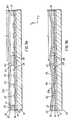
- Fig. 1shows the structure of two side-by-side conformal grating devices 5a and 5b in an unactuated state.
- the devicescan be operated by the application of an electrostatic force.
- the grating devices 5a and 5bare formed on top of a substrate 10, made of glass, metal, plastic or semiconductor materials, that is covered by a bottom conductive layer 12 which acts as an electrode to actuate the devices.
- the bottom conductive layer 12can be made of materials such as aluminum, titanium, gold, silver, tungsten, doped silicon or indium tin oxide.
- the bottom conductive layer 12is covered by a dielectric protective layer 14 followed by a spacer layer 18.
- a ribbon layer 20is formed which is covered by a reflective layer 22.
- the reflective layer 22is also a conductor in order to provide electrodes for the actuation of the conformal grating devices 5a and 5b.
- the reflective and conductive layer 22is patterned to provide electrodes to the two conformal grating devices 5a and 5b.
- the ribbon layer 20preferably comprises a material with a sufficient tensile stress to provide a large restoring force. Examples of ribbon materials are silicon nitride, titanium aluminide, and titanium oxide.
- the thickness and tensile stress of the ribbon layer 20are chosen to optimize performance by influencing the electrostatic force for actuation and the restoring force. These forces affect the voltage requirement, speed and resonance frequency of the conformal grating devices 5a and 5b.
- Each of the two devices 5a and 5bhas an associated elongated ribbon element 23a and 23b, respectively, patterned from the reflective and conductive layer 22 and the ribbon layer 20.
- the elongated ribbon elements 23a and 23bare supported by end supports 24a and 24b formed from the spacer layer 18 and by one or more intermediate supports 27.
- three intermediate supports 27are shown formed from the spacer layer 18. These intermediate supports 27 are uniformly separated in order to form four equal-width channels 25.
- the elongated ribbon elements 23a and 23bare secured to the end supports and to the intermediate supports 27.
- the end supports 24a and bare not defined other than at their edges facing the channel 25.
- a plurality of square standoffs 29is patterned at the bottom of the channels 25 from the standoff layer 14. These standoffs 29 reduce the possibility of the ribbon elements sticking when actuated.
- the standoffsmay also be patterned in shapes other than square; for example, rectangular or round.
- FIG. 2A top view of a four-device linear array of conformal grating devices 5a, 5b, 5c and 5d is shown in Fig. 2.
- the elongated ribbon elementsare depicted partially removed over the portion of the diagram below the line 2-2 in order to show the underlying structure.
- the intermediate supports 27must be completely hidden below the elongated ribbon elements 23a, 23b, 23c and 23d. Therefore, when viewed from the top, the intermediate supports must not be visible in the gaps 32 between the conformal grating devices 5a-5d.
- each of the conformal grating deviceshas three intermediate supports 27 with four equal-width channels 25.
- the center-to-center separation A of the intermediate supports 27defines the period of the conformal grating devices in the actuated state.
- the elongated ribbon elements 23a-23dare mechanically and electrically isolated from one another, allowing independent operation of the four conformal grating devices 5a-5d.
- the bottom conductive layer 12 of Fig. 1can be common to all of the devices.
- Fig. 3ais a side view, through line 3-3 of Fig. 2, of two channels 25 of the conformal grating device 5b in the unactuated state.
- Fig. 3bshows the same view of the actuated state.
- an attractive electrostatic forceis produced by applying a voltage difference between the bottom conductive layer 12 and the conducting layer 22 of the elongated ribbon element 23b.
- the ribbon element 23bis suspended flat between the supports. In this state, an incident light beam 30 is primarily reflected 33 into the mirror direction.
- a voltageis applied to the conformal grating device 5b, which deforms the elongated ribbon element 23b and produces a partially conformal grating with period A.
- Figs. 3bshows the device in the fully actuated state with the elongated ribbon element 23b in contact with the standoffs 29.
- the height difference between the bottom of element 23b and the top of the standoffs 29is chosen to be approximately 1 ⁇ 4 of the wavelength ⁇ of the incident light. The optimum height depends on the specific shape of the actuated device.
- the incident light beam 30is primarily diffracted into the +1 st order 35a and -1 st order 35b, with additional light diffracted into the +2 nd order 36a and -2 nd order 36b.
- a small amount of lightis diffracted into even higher orders and some is reflected.
- One or more of the diffracted orderscan be collected and used by the optical system, depending on the application.
- the applied voltageis removed, the forces due to the tensile stress and bending restores the ribbon element 23b to its original unactuated state.
- Figs. 4a and 4bshow a rotated side view through line 4-4 of Fig. 2 of the conformal grating device 5b in the unactuated and actuated states, respectively.
- the elongated ribbon element 23bis suspended by the end support 24b and the adjacent intermediate support 27 (not shown in this perspective).
- the application of a voltageactuates the device as illustrated in Fig. 4b.
- a linear array of conformal grating devicesis formed by arranging the devices as illustrated in Figs. 1-3 with the direction of the grating period A (the y direction) perpendicular to the array direction (the x direction).
- the diffracted ordersare then at various angles in the y-z plane and are perpendicular to the array direction.
- the diffracted ordersbecome spatially separated over a relatively short distance. This feature simplifies the optical system design and enables feasible designs in which the separation of orders can be done spatially without the need of Schlieren optics.
- the grating periodis parallel to the array directions which leads to a much larger distance needed for spatial separation of the diffracted orders.
- an array of conformal grating devicesthat is 4cm long (2000 devices 20 ⁇ m wide) illuminated by a 100 ⁇ m line of light.
- the orderswill become spatially separated in approximately 6 mm.
- a similar 4 cm linear array of prior art GLV devices with a 4 degree angular separation between diffracted orderswould require at least 60 cm for spatial separation, without the use of a Schlieren optical system.
- the grating period A in a conformal grating arrayis perpendicular to the array direction, the array can be made many periods wide, with no significant constraint on the number of periods possible. Increasing the number of periods improves the optical alignment tolerances and provides some built-in redundancy in case of local device failure. If a portion of a conformal grating device stops functioning, the optical beam can be repositioned to a working portion.
- Figs. 5 and 6show the modeled electromechanical operation of this particular device.
- Fig. 5is a plot of the position of the elongated ribbon element at the center of a channel as a function of applied voltage, illustrating the associated hysteresis.
- the center displacementincreases in approximately a quadratic manner until the pull-down voltage of 20.1 V is reached.
- the electrostatic forceovercomes the tensile restoring force and the ribbon slams into the substrate.
- Further increasing the applied voltagechanges the shape of the deformed ribbon, but cannot change the center position.
- the voltageWith the ribbon in contact with the substrate, the voltage can be reduced below the pull-down value while maintaining contact, until release at 10.8 V.
- This hysteresiscan be exploited to improve the optical performance of the device. It can also be used as a switch in certain applications.
- Fig. 6demonstrates how the grating profile may be modified by adjusting the applied voltage.
- the profile of two periods of the actuated deviceis shown at 12V (dotted line) and at 22V (solid line), with the ribbon and substrate in contact.
- contactmust first be established by applying a value larger than the pull-down voltage of 20.1 V. Because 12V is only slightly larger that the release voltage, only a small portion of the ribbon touches the substrate. This change in shape with voltage has an important impact on the diffraction efficiency of the device.
- Fig. 7is a plot of the diffraction efficiency of the device as a function of applied voltage, assuming an illumination wavelength of 550 nm and 100% reflectivity. Efficiency curves are shown for two cases: 1) an optical system that collects of the -1 and +1 diffracted orders and 2) a system that collects all of the diffracted orders. The curves for both cases show that the voltage can be adjusted to maximize the diffraction efficiency. For the first system the maximum occurs at about 14.5 V, whereas for the second it occurs at about 16V. In order to achieve the optimal optical performance with this particular design, it is necessary to first establish contact by applying a voltage larger than the pull-down voltage of 20.1 V. The voltage is then reduced to obtain the optimal shape.
- FIG. 8An alternate embodiment of conformal grating devices is shown in Fig. 8, which depicts a top view of a four-device linear array similar to Fig. 2.
- Each of the conformal grating devices 5a, 5b, 5c and 5dnow has an associated pair of elongated ribbon elements (51a, 52a), (51b, 52b), (51c, 52c) and (51d, 52d), respectively.
- This subdivision of each devicepermits fabrication of wider devices without significantly impacting optical performance.
- the preferred method of fabricationis to etch a sacrificial layer from the channel, thus releasing the ribbon elements.
- the gaps 55 between the elementsallow the etchant to access this sacrificial layer. Increasing the number of gaps 55 can therefore improve the etching process.
- the conformal grating devicesIn practice, it may be necessary to further subdivide the conformal grating devices into more than two.
- the elongated ribbon elementsare depicted partially removed over the portion of the diagram below the line 2-2 in order to show the underlying structure.
- the intermediate supports 27For best optical performance and maximum contrast, the intermediate supports 27 must be completely hidden below the elongated ribbon elements 51a, 52a, 51 b, 52b, 51 c, 52c, 51d and 52d. Therefore, when viewed from the top, the intermediate supports 27 must not penetrate into the gaps 55.
- the ribbon elements within a single conformal grating deviceare mechanically isolated, but electrically coupled. They therefore operate in unison when a voltage is applied.
- Figs. 9a and 9bshow an alternate embodiment that reduces this problem.
- the side viewis the same as in Fig. 3a and 3b.
- Fig. 9adepicts the two channels 25 between the three intermediate supports 27 of the device in the unactuated state.
- Fig. 9bshows the same view of the actuated state.
- the ribbon element 23bIn the unactuated state, with no voltage applied to the device, the ribbon element 23b is suspended flat above the intermediate supports 27 by the two end supports 24a and 24b (see Fig. 2), leaving a small gap 60 between the top of the intermediate supports 27 and the bottom of the ribbon element 23b.
- a voltageis applied to actuate the device, the bottom of the ribbon element 23b makes contact with the top of the intermediate supports and a partially conforming grating is created.
- Figs. 3bshows the device in the fully actuated state with the elongated ribbon element 23b also touching the standoffs 29.
Landscapes
- Physics & Mathematics (AREA)
- General Physics & Mathematics (AREA)
- Optics & Photonics (AREA)
- Mechanical Light Control Or Optical Switches (AREA)
- Diffracting Gratings Or Hologram Optical Elements (AREA)
- Micromachines (AREA)
Description
- This invention relates to a micromechanical device for spatially and temporally modulating an incident beam of light and, more particularly, to an electromechanical device with a conformal grating structure that causes diffraction of the incident light beam.
- Electromechanical spatial light modulators with a variety of designs have been used in applications such as display, optical processing, printing, optical data storage and spectroscopy. These modulators produce spatial variations in the phase and/or amplitude of an incident beam of light using arrays of individually addressable devices.
- Spatial phase modulation of an incident beam can be accomplished by arrays of individually addressable deformable mirrors. Such devices can be from a deformable reflective membrane suspended over a grid of supports, as described in U. S. Patent No. 4,441,791, issued April 10, 1984 to Hornbeck, entitled "Deformable Mirror Light Modulator." However, because of the membrane and support structure, these particular deformable mirrors are very inefficient. More efficient deformable mirror designs are disclosed in U. S Patent 5,170,283, issued December 8, 1992 to O'Brien et al., entitled "Silicon Spatial Light Modulator," and in U. S. Patent 5,844,711, issued December 1, 1998 to Long, Jr., entitled "Tunable Spatial Light Modulator."
- Another class of electromechanical spatial light modulators has devices with a periodic sequence of reflective elements that form electromechanical phase gratings. In such devices, the incident light beam is selectively reflected or diffracted into a number of discrete orders. Depending on the application, one or more of these diffracted orders may be collected and used by the optical system. For many applications, electromechanical phase gratings are preferable to deformable mirrors. Electromechanical phase gratings can be formed in metallized elastomer gels; see U. S. Patent 4,626,920, issued December 2, 1986 to Glenn, entitled "Solid State Light Modulator Structure," and U. S. Patent 4,857,978, issued August 15, 1989 to Goldburt et al., entitled "Solid State Light Modulator Incorporating Metallized Gel and Method of Metallization." The electrodes below the elastomer are patterned so that the application of a voltage deforms the elastomer producing a nearly sinusoidal phase grating. These types of devices have been successfully used in color projection displays; see "Metallized viscoelastic control layers for light-valve projection displays,"
Displays 16, 1995, pages 13-20, and "Full-colour diffraction-based optical system for light-valve projection displays,"Displays 16, 1995, pages 27-34. - An electromechanical phase grating with a much faster response time can be made of suspended micromechanical ribbon elements, as described in U. S. Patent No. 5,311,360, issued May 10, 1994, to Bloom et al., entitled "Method and Apparatus for Modulating a Light Beam." This device, also known as a grating light valve (GLV), can be fabricated with CMOS-like processes on silicon. Improvements in the device were later described by Bloom et al. that included: 1) patterned raised areas beneath the ribbons to minimize contact area to obviate stiction between the ribbons and the substrate, and 2) an alternative device design in which the spacing between ribbons was decreased and alternate ribbons were actuated to produce good contrast. See U. S. Patent No. 5,459,610, issued October 17, 1995 to Bloom et al., entitled "Deformable Grating Apparatus for Modulating a Light Beam and Including Means for Obviating Stiction Between Grating Elements and Underlying Substrate." Bloom et al. also presented a method for fabricating the device; see U. S. Patent No. 5,677,783, issued October 14, 1997, entitled "Method of Making a Deformable Grating Apparatus for Modulating a Light Beam and Including Means for Obviating Stiction Between Grating Elements and Underlying Substrate." Additional improvements in the design and fabrication of the GLV were described in U. S. Patent No. 5,841,579, issued November 124, 1998 to Bloom et al., entitled "Flat Diffraction Grating Light Valve," and in U. S. Patent No. 5,661,592, issued August 26, 1997 to Bornstein et al., entitled "Method of Making and an Apparatus for a Flat Diffraction Grating Light Valve." Linear arrays of GLV devices can be used for display and printing as described in U. S. Patent No. 5,982,553, issued November 9, 1999 to Bloom et al., entitled "Display Device Incorporating One-Dimensional Grating Light-Valve Array." With linear GLV arrays of this type, the diffraction direction is not perpendicular to the array direction, which increases the complexity of the optical system required for separation of the diffracted orders. Furthermore, the active region of the array is relatively narrow requiring good alignment of line illumination over the entire length of the array, typically to within 10-30 microns over a few centimeters of length. The line illumination then also needs to be very straight over the entire linear array.
- There is a need therefore for a linear array of grating devices that has a large active region with the diffraction direction perpendicular to the array direction. Furthermore, the device must be able to diffract light efficiently at high speed into discrete orders and the device fabrication must be compatible with CMOS-like processes.
- The need is met according to the present invention by providing a mechanical grating device as defined in
claim 1 for modulating an incident beam of light by diffraction. - The present invention has the advantage of having a wide active region compared to prior art grating light valve arrays, thereby facilitating alignment of the device and allowing tolerances on the illumination system to be relaxed. The device has the further advantage that the diffraction direction is perpendicular to the long axis of the array, thereby allowing simplification of the optics employed to collect the light diffracted by the array.
- Fig. 1 is a perspective, partially cut-away view of the spatial light modulator with conformal grating devices of the present invention, showing two devices in a linear array;
- Fig. 2 is a top view of the spatial light modulator of the present invention, showing four devices in a linear array;
- Fig. 3a and b are cross-sectional views through line 3-3 in Fig. 1 showing the device in an unactuated state and an actuated state, respectively;
- Fig. 4a and b are a cross-sectional views through line 4-4 in Fig. 1 showing the device in an unactuated state and an actuated state, respectively;
- Fig. 5 is a plot showing device position as a function of applied voltage;
- Fig. 6 is a diagram showing the deflected element profile in response to two different actuation voltages in device;
- Fig. 7 is a plot showing diffraction efficiency of the modulator as a function of applied voltage for two different optical system;
- Fig. 8 is a top view of an alternate embodiment of the spatial light modulator; and
- Fig. 9a and b are cross sectional views of a further alternative embodiment of the spatial light modulator according to the present invention.
- The conformal grating devices of the preferred embodiment of the present invention are illustrated in Figs. 1-4. Fig. 1 shows the structure of two side-by-side
conformal grating devices grating devices substrate 10, made of glass, metal, plastic or semiconductor materials, that is covered by a bottomconductive layer 12 which acts as an electrode to actuate the devices. The bottomconductive layer 12 can be made of materials such as aluminum, titanium, gold, silver, tungsten, doped silicon or indium tin oxide. The bottomconductive layer 12 is covered by a dielectricprotective layer 14 followed by aspacer layer 18. On top of thespacer layer 18, aribbon layer 20 is formed which is covered by areflective layer 22. In the present embodiment, thereflective layer 22 is also a conductor in order to provide electrodes for the actuation of theconformal grating devices conductive layer 22 is patterned to provide electrodes to the twoconformal grating devices ribbon layer 20 preferably comprises a material with a sufficient tensile stress to provide a large restoring force. Examples of ribbon materials are silicon nitride, titanium aluminide, and titanium oxide. The thickness and tensile stress of theribbon layer 20 are chosen to optimize performance by influencing the electrostatic force for actuation and the restoring force. These forces affect the voltage requirement, speed and resonance frequency of theconformal grating devices - Each of the two
devices elongated ribbon element conductive layer 22 and theribbon layer 20. Theelongated ribbon elements end supports spacer layer 18 and by one or moreintermediate supports 27. In Fig. 1, threeintermediate supports 27 are shown formed from thespacer layer 18. Theseintermediate supports 27 are uniformly separated in order to form four equal-width channels 25. Theelongated ribbon elements intermediate supports 27. The end supports 24a and b are not defined other than at their edges facing thechannel 25. A plurality ofsquare standoffs 29 is patterned at the bottom of thechannels 25 from thestandoff layer 14. Thesestandoffs 29 reduce the possibility of the ribbon elements sticking when actuated. The standoffs may also be patterned in shapes other than square; for example, rectangular or round. - A top view of a four-device linear array of
conformal grating devices intermediate supports 27 must be completely hidden below theelongated ribbon elements gaps 32 between theconformal grating devices 5a-5d. Here each of the conformal grating devices has threeintermediate supports 27 with four equal-width channels 25. - The center-to-center separation A of the
intermediate supports 27 defines the period of the conformal grating devices in the actuated state. Theelongated ribbon elements 23a-23d are mechanically and electrically isolated from one another, allowing independent operation of the fourconformal grating devices 5a-5d. The bottomconductive layer 12 of Fig. 1 can be common to all of the devices. - Fig. 3a is a side view, through line 3-3 of Fig. 2, of two
channels 25 of the conformalgrating device 5b in the unactuated state. Fig. 3b shows the same view of the actuated state. For operation of the device, an attractive electrostatic force is produced by applying a voltage difference between the bottomconductive layer 12 and theconducting layer 22 of theelongated ribbon element 23b. In the unactuated state (see Fig. 3a), with no voltage difference, theribbon element 23b is suspended flat between the supports. In this state, anincident light beam 30 is primarily reflected 33 into the mirror direction. To obtain the actuated state, a voltage is applied to the conformalgrating device 5b, which deforms theelongated ribbon element 23b and produces a partially conformal grating with period A. Figs. 3b shows the device in the fully actuated state with theelongated ribbon element 23b in contact with thestandoffs 29. The height difference between the bottom ofelement 23b and the top of thestandoffs 29 is chosen to be approximately ¼ of the wavelength λ of the incident light. The optimum height depends on the specific shape of the actuated device. In the actuated state, theincident light beam 30 is primarily diffracted into the +1storder 35a and -1storder 35b, with additional light diffracted into the +2nd order 36a and -2ndorder 36b. A small amount of light is diffracted into even higher orders and some is reflected. For light incident perpendicular to the surface of the device, the angle θm between the incident beam and the mth order diffracted beam is given by
where m is an integer. - One or more of the diffracted orders can be collected and used by the optical system, depending on the application. When the applied voltage is removed, the forces due to the tensile stress and bending restores the
ribbon element 23b to its original unactuated state. - Figs. 4a and 4b show a rotated side view through line 4-4 of Fig. 2 of the conformal
grating device 5b in the unactuated and actuated states, respectively. Theelongated ribbon element 23b is suspended by theend support 24b and the adjacent intermediate support 27 (not shown in this perspective). The application of a voltage actuates the device as illustrated in Fig. 4b. - In the preferred embodiment, a linear array of conformal grating devices is formed by arranging the devices as illustrated in Figs. 1-3 with the direction of the grating period A (the y direction) perpendicular to the array direction (the x direction). The diffracted orders are then at various angles in the y-z plane and are perpendicular to the array direction. Even with a large linear array consisting, possibly, of several thousand devices illuminated by a narrow line of light, the diffracted orders become spatially separated over a relatively short distance. This feature simplifies the optical system design and enables feasible designs in which the separation of orders can be done spatially without the need of Schlieren optics.
- In a linear array made from conventional GLV devices, the grating period is parallel to the array directions which leads to a much larger distance needed for spatial separation of the diffracted orders. As a comparative example, let us consider an array of conformal grating devices that is 4cm long (2000
devices 20 µm wide) illuminated by a 100 µm line of light. For devices with a period chosen such that the diffracted orders are angularly separated by 1 degree, the orders will become spatially separated in approximately 6 mm. A similar 4 cm linear array of prior art GLV devices with a 4 degree angular separation between diffracted orders would require at least 60 cm for spatial separation, without the use of a Schlieren optical system. - Furthermore, because the grating period A in a conformal grating array is perpendicular to the array direction, the array can be made many periods wide, with no significant constraint on the number of periods possible. Increasing the number of periods improves the optical alignment tolerances and provides some built-in redundancy in case of local device failure. If a portion of a conformal grating device stops functioning, the optical beam can be repositioned to a working portion.
- To understand the electromechanical and optical operation of the conformal grating device in more detail, it is helpful to examine the expected performance of a realistic design with the following materials and parameters:
- Substrate material: silicon
- Bottom conductive layer: doped silicon
- Protective layer: silicon dioxide, thickness = 50 nm
- Spacer layer: silicon dioxide, thickness = 150 nm
- Ribbon layer: silicon nitride, thickness = 100 nm, tensile stress = 600 Mpa
- Reflective and conductive layer: aluminum, thickness = 50 nm
- Grating period A = 20 µm
- Suspended length of elongated ribbon element = 16 µm
- Width of elongated ribbon element w = 30 µm
- Width of intermediate supports = 4 µm
- Figs. 5 and 6 show the modeled electromechanical operation of this particular device. Fig. 5 is a plot of the position of the elongated ribbon element at the center of a channel as a function of applied voltage, illustrating the associated hysteresis. As the voltage is increased from 0 V, the center displacement increases in approximately a quadratic manner until the pull-down voltage of 20.1 V is reached. At this voltage, the electrostatic force overcomes the tensile restoring force and the ribbon slams into the substrate. Further increasing the applied voltage changes the shape of the deformed ribbon, but cannot change the center position. With the ribbon in contact with the substrate, the voltage can be reduced below the pull-down value while maintaining contact, until release at 10.8 V. This hysteresis can be exploited to improve the optical performance of the device. It can also be used as a switch in certain applications.
- Fig. 6 demonstrates how the grating profile may be modified by adjusting the applied voltage. The profile of two periods of the actuated device is shown at 12V (dotted line) and at 22V (solid line), with the ribbon and substrate in contact. To obtain this 12V profile, contact must first be established by applying a value larger than the pull-down voltage of 20.1 V. Because 12V is only slightly larger that the release voltage, only a small portion of the ribbon touches the substrate. This change in shape with voltage has an important impact on the diffraction efficiency of the device.
- Fig. 7 is a plot of the diffraction efficiency of the device as a function of applied voltage, assuming an illumination wavelength of 550 nm and 100% reflectivity. Efficiency curves are shown for two cases: 1) an optical system that collects of the -1 and +1 diffracted orders and 2) a system that collects all of the diffracted orders. The curves for both cases show that the voltage can be adjusted to maximize the diffraction efficiency. For the first system the maximum occurs at about 14.5 V, whereas for the second it occurs at about 16V. In order to achieve the optimal optical performance with this particular design, it is necessary to first establish contact by applying a voltage larger than the pull-down voltage of 20.1 V. The voltage is then reduced to obtain the optimal shape.
- An alternate embodiment of conformal grating devices is shown in Fig. 8, which depicts a top view of a four-device linear array similar to Fig. 2. Each of the
conformal grating devices gaps 55 between the elements allow the etchant to access this sacrificial layer. Increasing the number ofgaps 55 can therefore improve the etching process. In practice, it may be necessary to further subdivide the conformal grating devices into more than two. The elongated ribbon elements are depicted partially removed over the portion of the diagram below the line 2-2 in order to show the underlying structure. For best optical performance and maximum contrast, theintermediate supports 27 must be completely hidden below theelongated ribbon elements intermediate supports 27 must not penetrate into thegaps 55. The ribbon elements within a single conformal grating device are mechanically isolated, but electrically coupled. They therefore operate in unison when a voltage is applied. - The conformal grating devices described in the above embodiments have intermediate supports attached to the elongated ribbon elements. To obtain very high contrast, these supports must be completely hidden when the devices are not actuated and the ribbon elements must be completely flat. However, in practice, the fabrication causes some nonuniformity in the profile of the ribbon element just above the intermediate supports. The nonuniformity produces a weak grating reducing the contrast of the device. Figs. 9a and 9b show an alternate embodiment that reduces this problem. The side view is the same as in Fig. 3a and 3b. Fig. 9a depicts the two
channels 25 between the threeintermediate supports 27 of the device in the unactuated state. Fig. 9b shows the same view of the actuated state. In the unactuated state, with no voltage applied to the device, theribbon element 23b is suspended flat above theintermediate supports 27 by the two end supports 24a and 24b (see Fig. 2), leaving asmall gap 60 between the top of theintermediate supports 27 and the bottom of theribbon element 23b. When a voltage is applied to actuate the device, the bottom of theribbon element 23b makes contact with the top of the intermediate supports and a partially conforming grating is created. Figs. 3b shows the device in the fully actuated state with theelongated ribbon element 23b also touching thestandoffs 29.

Claims (17)
- A mechanical grating device for modulating an incident beam of light by diffraction, comprising:a) an elongated element (23a, 23b, 23c, 23d) including a light reflective surface; and able to deform between first and second operating states;b) a pair of end supports for supporting the elongated element at both ends over a substrate (10);c) at least one intermediate support (27) between the end supports; andd) means (12, 22) for applying a force to the elongated element,characterized in that the means for applying a force and the intermediate support cooperate in the second operating state, to cause the elongated element to deform around the intermediate support, toward the substrate, such that said elongated element thereby functions as a diffraction grating.
- The mechanical grating device claimed in claim 1, wherein in the first operating state, the elongated element functions as a plane reflector.
- The mechanical grating device claimed in claim 1, wherein the intermediate support contacts the elongated element only when in the second operating state.
- The mechanical grating device claimed in claim 1, wherein the elongated element is supported under tension.
- The mechanical grating device claimed in claim 1, further including a stand off (29) located on the substrate under the elongated element to prevent the elongated element from sticking to the substrate when the elongated element is deformed.
- The mechanical grating device claimed in claim 1, wherein the force is an electrostatic force.
- The mechanical grating device claimed in claim 6, wherein the elongated element includes a first conductor (22), and the substrate under the elongated element includes a second conductor (12) for applying a voltage to generate the electrostatic force.
- The mechanical grating device claimed in claim 1, wherein the elongated element comprises a plurality of parallel spaced apart portions.
- The mechanical grating device claimed in claim 8, wherein the intermediate support comprises a plurality of spaced apart portions arranged such that the intermediate support is not visible when viewing the light reflective surface of the elongated element.
- The mechanical grating device claimed in claim 1, wherein the elongated element is secured to the at least one intermediate support and the end supports.
- The mechanical grating device claimed in claim 1, wherein a plurality of intermediate supports is placed between the end supports with a uniform separation so as to form equal-width channels.
- The mechanical grating device claimed in claim 1, wherein in the first operating state the elongated element is suspended flat and in the second operating state the elongated element has at least two periods.
- The mechanical grating device claimed in claim 9, wherein the plurality of parallel spaced apart portions is electrically coupled, so as to operate in unison.
- A mechanical grating device array for spatially modulating an incident beam of light by diffraction, comprising a plurality of mechanical grating devices, as defined in one of claims 1 to 9.
- The mechanical grating device array claimed in claim 14, wherein the plurality of mechanical grating devices is arranged in a line such that a diffraction grating period is perpendicular to the line.
- The mechanical grating device array claimed in claim 14, wherein the grating devices are arranged in a two dimensional array.
- A method of operating the mechanical grating device claimed in claim 7, wherein the mechanical grating device exhibits hysteresis, comprising the steps of:a) applying a voltage across the conductors of the device to switch the device from the first state to the second state; andb) decreasing the voltage to hold the elongated element in a more optimal second state.
Applications Claiming Priority (2)
| Application Number | Priority Date | Filing Date | Title |
|---|---|---|---|
| US09/491,354US6307663B1 (en) | 2000-01-26 | 2000-01-26 | Spatial light modulator with conformal grating device |
| US491354 | 2000-01-26 |
Publications (3)
| Publication Number | Publication Date |
|---|---|
| EP1122577A2 EP1122577A2 (en) | 2001-08-08 |
| EP1122577A3 EP1122577A3 (en) | 2003-11-12 |
| EP1122577B1true EP1122577B1 (en) | 2006-08-02 |
Family
ID=23951835
Family Applications (1)
| Application Number | Title | Priority Date | Filing Date |
|---|---|---|---|
| EP01200128AExpired - LifetimeEP1122577B1 (en) | 2000-01-26 | 2001-01-15 | Spatial light modulator with conformal grating device |
Country Status (4)
| Country | Link |
|---|---|
| US (2) | US6307663B1 (en) |
| EP (1) | EP1122577B1 (en) |
| JP (1) | JP2001215317A (en) |
| DE (1) | DE60121838T2 (en) |
Cited By (55)
| Publication number | Priority date | Publication date | Assignee | Title |
|---|---|---|---|---|
| US7554714B2 (en) | 2004-09-27 | 2009-06-30 | Idc, Llc | Device and method for manipulation of thermal response in a modulator |
| US7564612B2 (en) | 2004-09-27 | 2009-07-21 | Idc, Llc | Photonic MEMS and structures |
| US7612933B2 (en) | 2008-03-27 | 2009-11-03 | Qualcomm Mems Technologies, Inc. | Microelectromechanical device with spacing layer |
| US7612932B2 (en) | 2004-09-27 | 2009-11-03 | Idc, Llc | Microelectromechanical device with optical function separated from mechanical and electrical function |
| US7630119B2 (en) | 2004-09-27 | 2009-12-08 | Qualcomm Mems Technologies, Inc. | Apparatus and method for reducing slippage between structures in an interferometric modulator |
| US7629197B2 (en) | 2006-10-18 | 2009-12-08 | Qualcomm Mems Technologies, Inc. | Spatial light modulator |
| US7630121B2 (en) | 2007-07-02 | 2009-12-08 | Qualcomm Mems Technologies, Inc. | Electromechanical device with optical function separated from mechanical and electrical function |
| US7643199B2 (en) | 2007-06-19 | 2010-01-05 | Qualcomm Mems Technologies, Inc. | High aperture-ratio top-reflective AM-iMod displays |
| US7643202B2 (en) | 2007-05-09 | 2010-01-05 | Qualcomm Mems Technologies, Inc. | Microelectromechanical system having a dielectric movable membrane and a mirror |
| US7649671B2 (en) | 2006-06-01 | 2010-01-19 | Qualcomm Mems Technologies, Inc. | Analog interferometric modulator device with electrostatic actuation and release |
| US7663794B2 (en) | 2004-09-27 | 2010-02-16 | Qualcomm Mems Technologies, Inc. | Methods and devices for inhibiting tilting of a movable element in a MEMS device |
| US7704772B2 (en) | 2004-05-04 | 2010-04-27 | Qualcomm Mems Technologies, Inc. | Method of manufacture for microelectromechanical devices |
| US7715085B2 (en) | 2007-05-09 | 2010-05-11 | Qualcomm Mems Technologies, Inc. | Electromechanical system having a dielectric movable membrane and a mirror |
| US7715079B2 (en) | 2007-12-07 | 2010-05-11 | Qualcomm Mems Technologies, Inc. | MEMS devices requiring no mechanical support |
| US7742220B2 (en) | 2007-03-28 | 2010-06-22 | Qualcomm Mems Technologies, Inc. | Microelectromechanical device and method utilizing conducting layers separated by stops |
| US7746539B2 (en) | 2008-06-25 | 2010-06-29 | Qualcomm Mems Technologies, Inc. | Method for packing a display device and the device obtained thereof |
| US7768690B2 (en) | 2008-06-25 | 2010-08-03 | Qualcomm Mems Technologies, Inc. | Backlight displays |
| US7773286B2 (en) | 2007-09-14 | 2010-08-10 | Qualcomm Mems Technologies, Inc. | Periodic dimple array |
| US7782517B2 (en) | 2007-06-21 | 2010-08-24 | Qualcomm Mems Technologies, Inc. | Infrared and dual mode displays |
| US7787173B2 (en) | 2004-09-27 | 2010-08-31 | Qualcomm Mems Technologies, Inc. | System and method for multi-level brightness in interferometric modulation |
| US7791027B2 (en) | 2006-01-31 | 2010-09-07 | Ahura Scientific Inc. | Apparatus and method providing a hand-held spectrometer |
| US7835061B2 (en) | 2006-06-28 | 2010-11-16 | Qualcomm Mems Technologies, Inc. | Support structures for free-standing electromechanical devices |
| US7839557B2 (en) | 2004-09-27 | 2010-11-23 | Qualcomm Mems Technologies, Inc. | Method and device for multistate interferometric light modulation |
| US7847999B2 (en) | 2007-09-14 | 2010-12-07 | Qualcomm Mems Technologies, Inc. | Interferometric modulator display devices |
| US7855826B2 (en) | 2008-08-12 | 2010-12-21 | Qualcomm Mems Technologies, Inc. | Method and apparatus to reduce or eliminate stiction and image retention in interferometric modulator devices |
| US7859740B2 (en) | 2008-07-11 | 2010-12-28 | Qualcomm Mems Technologies, Inc. | Stiction mitigation with integrated mech micro-cantilevers through vertical stress gradient control |
| US7884989B2 (en) | 2005-05-27 | 2011-02-08 | Qualcomm Mems Technologies, Inc. | White interferometric modulators and methods for forming the same |
| US7889415B2 (en) | 2004-09-27 | 2011-02-15 | Qualcomm Mems Technologies, Inc. | Device having a conductive light absorbing mask and method for fabricating same |
| US7898723B2 (en) | 2008-04-02 | 2011-03-01 | Qualcomm Mems Technologies, Inc. | Microelectromechanical systems display element with photovoltaic structure |
| US7936497B2 (en) | 2004-09-27 | 2011-05-03 | Qualcomm Mems Technologies, Inc. | MEMS device having deformable membrane characterized by mechanical persistence |
| US7944604B2 (en) | 2008-03-07 | 2011-05-17 | Qualcomm Mems Technologies, Inc. | Interferometric modulator in transmission mode |
| US7944599B2 (en) | 2004-09-27 | 2011-05-17 | Qualcomm Mems Technologies, Inc. | Electromechanical device with optical function separated from mechanical and electrical function |
| US7952787B2 (en) | 2006-06-30 | 2011-05-31 | Qualcomm Mems Technologies, Inc. | Method of manufacturing MEMS devices providing air gap control |
| US7969638B2 (en) | 2008-04-10 | 2011-06-28 | Qualcomm Mems Technologies, Inc. | Device having thin black mask and method of fabricating the same |
| US7982700B2 (en) | 2004-09-27 | 2011-07-19 | Qualcomm Mems Technologies, Inc. | Conductive bus structure for interferometric modulator array |
| US7999993B2 (en) | 2004-09-27 | 2011-08-16 | Qualcomm Mems Technologies, Inc. | Reflective display device having viewable display on both sides |
| US8008736B2 (en) | 2004-09-27 | 2011-08-30 | Qualcomm Mems Technologies, Inc. | Analog interferometric modulator device |
| US8023167B2 (en) | 2008-06-25 | 2011-09-20 | Qualcomm Mems Technologies, Inc. | Backlight displays |
| US8054527B2 (en) | 2007-10-23 | 2011-11-08 | Qualcomm Mems Technologies, Inc. | Adjustably transmissive MEMS-based devices |
| US8058549B2 (en) | 2007-10-19 | 2011-11-15 | Qualcomm Mems Technologies, Inc. | Photovoltaic devices with integrated color interferometric film stacks |
| US8081373B2 (en) | 2007-07-31 | 2011-12-20 | Qualcomm Mems Technologies, Inc. | Devices and methods for enhancing color shift of interferometric modulators |
| US8081370B2 (en) | 2004-09-27 | 2011-12-20 | Qualcomm Mems Technologies, Inc. | Support structures for electromechanical systems and methods of fabricating the same |
| US8115987B2 (en) | 2007-02-01 | 2012-02-14 | Qualcomm Mems Technologies, Inc. | Modulating the intensity of light from an interferometric reflector |
| US8164821B2 (en) | 2008-02-22 | 2012-04-24 | Qualcomm Mems Technologies, Inc. | Microelectromechanical device with thermal expansion balancing layer or stiffening layer |
| US8270056B2 (en) | 2009-03-23 | 2012-09-18 | Qualcomm Mems Technologies, Inc. | Display device with openings between sub-pixels and method of making same |
| US8270062B2 (en) | 2009-09-17 | 2012-09-18 | Qualcomm Mems Technologies, Inc. | Display device with at least one movable stop element |
| US8358266B2 (en) | 2008-09-02 | 2013-01-22 | Qualcomm Mems Technologies, Inc. | Light turning device with prismatic light turning features |
| US8488228B2 (en) | 2009-09-28 | 2013-07-16 | Qualcomm Mems Technologies, Inc. | Interferometric display with interferometric reflector |
| US8659816B2 (en) | 2011-04-25 | 2014-02-25 | Qualcomm Mems Technologies, Inc. | Mechanical layer and methods of making the same |
| US8797632B2 (en) | 2010-08-17 | 2014-08-05 | Qualcomm Mems Technologies, Inc. | Actuation and calibration of charge neutral electrode of a display device |
| US8817357B2 (en) | 2010-04-09 | 2014-08-26 | Qualcomm Mems Technologies, Inc. | Mechanical layer and methods of forming the same |
| US8941631B2 (en) | 2007-11-16 | 2015-01-27 | Qualcomm Mems Technologies, Inc. | Simultaneous light collection and illumination on an active display |
| US8963159B2 (en) | 2011-04-04 | 2015-02-24 | Qualcomm Mems Technologies, Inc. | Pixel via and methods of forming the same |
| US9057872B2 (en) | 2010-08-31 | 2015-06-16 | Qualcomm Mems Technologies, Inc. | Dielectric enhanced mirror for IMOD display |
| US9134527B2 (en) | 2011-04-04 | 2015-09-15 | Qualcomm Mems Technologies, Inc. | Pixel via and methods of forming the same |
Families Citing this family (95)
| Publication number | Priority date | Publication date | Assignee | Title |
|---|---|---|---|---|
| US6724125B2 (en) | 1999-03-30 | 2004-04-20 | Massachusetts Institute Of Technology | Methods and apparatus for diffractive optical processing using an actuatable structure |
| US6960305B2 (en)* | 1999-10-26 | 2005-11-01 | Reflectivity, Inc | Methods for forming and releasing microelectromechanical structures |
| US6639713B2 (en) | 2000-04-25 | 2003-10-28 | Umachines, Inc. | Silicon micromachined optical device |
| US6709886B2 (en) | 2000-04-25 | 2004-03-23 | Umachines, Inc. | Method of fabricating micromachined devices |
| US6411425B1 (en)* | 2000-09-27 | 2002-06-25 | Eastman Kodak Company | Electromechanical grating display system with spatially separated light beams |
| JP2002162599A (en)* | 2000-11-24 | 2002-06-07 | Sony Corp | Stereoscopic image display device |
| US6384959B1 (en)* | 2001-01-09 | 2002-05-07 | Eastman Kodak Company | Optical data modulation system with self-damped electromechanical conformal grating |
| US6661561B2 (en)* | 2001-03-26 | 2003-12-09 | Creo Inc. | High frequency deformable mirror device |
| US6856448B2 (en)* | 2001-03-26 | 2005-02-15 | Creo Inc. | Spatial light modulator |
| US6594060B2 (en)* | 2001-03-29 | 2003-07-15 | Eastman Kodak Company | Electromechanical conformal grating device with improved optical efficiency and contrast |
| FI20010917A7 (en)* | 2001-05-03 | 2002-11-04 | Nokia Corp | Electrically reconfigurable optical devices and method for forming them |
| US6621615B2 (en) | 2001-07-25 | 2003-09-16 | Eastman Kodak Company | Method and system for image display |
| US6587253B2 (en)* | 2001-08-16 | 2003-07-01 | Silicon Light Machines | Enhance thermal stability through optical segmentation |
| US6594090B2 (en) | 2001-08-27 | 2003-07-15 | Eastman Kodak Company | Laser projection display system |
| US7046410B2 (en) | 2001-10-11 | 2006-05-16 | Polychromix, Inc. | Actuatable diffractive optical processor |
| US6611380B2 (en) | 2001-12-21 | 2003-08-26 | Eastman Kodak Company | System and method for calibration of display system with linear array modulator |
| JP3755460B2 (en)* | 2001-12-26 | 2006-03-15 | ソニー株式会社 | Electrostatically driven MEMS element and manufacturing method thereof, optical MEMS element, light modulation element, GLV device, laser display, and MEMS apparatus |
| US6577429B1 (en) | 2002-01-15 | 2003-06-10 | Eastman Kodak Company | Laser projection display system |
| KR100908510B1 (en)* | 2002-02-26 | 2009-07-20 | 유니-픽셀 디스플레이스, 인코포레이티드 | Air gap spontaneous mechanism |
| US6590695B1 (en) | 2002-02-26 | 2003-07-08 | Eastman Kodak Company | Micro-mechanical polarization-based modulator |
| WO2003079384A2 (en)* | 2002-03-11 | 2003-09-25 | Uni-Pixel Displays, Inc. | Double-electret mems actuator |
| US6768585B2 (en) | 2002-05-02 | 2004-07-27 | Eastman Kodak Company | Monocentric autostereoscopic optical apparatus using a scanned linear electromechanical modulator |
| WO2003094138A2 (en)* | 2002-05-06 | 2003-11-13 | Uni-Pixel Displays, Inc. | Field sequential color efficiency |
| US6800212B2 (en)* | 2002-05-15 | 2004-10-05 | The Regents Of The University Of California | Fabrication of optical components using Si, SiGe, SiGeC, and chemical endpoint detection |
| US6678085B2 (en) | 2002-06-12 | 2004-01-13 | Eastman Kodak Company | High-contrast display system with scanned conformal grating device |
| US6908201B2 (en)* | 2002-06-28 | 2005-06-21 | Silicon Light Machines Corporation | Micro-support structures |
| US6779892B2 (en)* | 2002-07-26 | 2004-08-24 | Eastman Kodak Company | Monocentric autostereoscopic optical display having an expanded color gamut |
| US6844960B2 (en)* | 2002-09-24 | 2005-01-18 | Eastman Kodak Company | Microelectromechanical device with continuously variable displacement |
| US6967986B2 (en)* | 2002-10-16 | 2005-11-22 | Eastman Kodak Company | Light modulation apparatus using a VCSEL array with an electromechanical grating device |
| US6802613B2 (en) | 2002-10-16 | 2004-10-12 | Eastman Kodak Company | Broad gamut color display apparatus using an electromechanical grating device |
| US6747785B2 (en)* | 2002-10-24 | 2004-06-08 | Hewlett-Packard Development Company, L.P. | MEMS-actuated color light modulator and methods |
| US6807010B2 (en)* | 2002-11-13 | 2004-10-19 | Eastman Kodak Company | Projection display apparatus having both incoherent and laser light sources |
| US6947459B2 (en)* | 2002-11-25 | 2005-09-20 | Eastman Kodak Company | Organic vertical cavity laser and imaging system |
| US6717714B1 (en)* | 2002-12-16 | 2004-04-06 | Eastman Kodak Company | Method and system for generating enhanced gray levels in an electromechanical grating display |
| US7057819B1 (en)* | 2002-12-17 | 2006-06-06 | Silicon Light Machines Corporation | High contrast tilting ribbon blazed grating |
| US6724515B1 (en)* | 2002-12-31 | 2004-04-20 | Eastman Kodak Company | Conformal grating device for producing enhanced gray levels |
| JP2004219843A (en)* | 2003-01-16 | 2004-08-05 | Seiko Epson Corp | Optical modulator, display device and manufacturing method thereof |
| US6863382B2 (en)* | 2003-02-06 | 2005-03-08 | Eastman Kodak Company | Liquid emission device having membrane with individually deformable portions, and methods of operating and manufacturing same |
| US6930817B2 (en)* | 2003-04-25 | 2005-08-16 | Palo Alto Research Center Incorporated | Configurable grating based on surface relief pattern for use as a variable optical attenuator |
| CN1297830C (en)* | 2003-06-05 | 2007-01-31 | 华新丽华股份有限公司 | Producing method for raster structure |
| US7111943B2 (en)* | 2003-07-28 | 2006-09-26 | Eastman Kodak Company | Wide field display using a scanned linear light modulator array |
| US6886940B2 (en)* | 2003-08-28 | 2005-05-03 | Eastman Kodak Company | Autostereoscopic display for multiple viewers |
| US20050073471A1 (en)* | 2003-10-03 | 2005-04-07 | Uni-Pixel Displays, Inc. | Z-axis redundant display/multilayer display |
| US7148910B2 (en)* | 2003-11-06 | 2006-12-12 | Eastman Kodak Company | High-speed pulse width modulation system and method for linear array spatial light modulators |
| CN1902673B (en)* | 2003-11-14 | 2011-06-15 | 单方图素显示股份有限公司 | Matrix addressing device and display and system comprising same |
| US6984039B2 (en)* | 2003-12-01 | 2006-01-10 | Eastman Kodak Company | Laser projector having silhouette blanking for objects in the output light path |
| US7274500B2 (en)* | 2003-12-03 | 2007-09-25 | Eastman Kodak Company | Display system incorporating trilinear electromechanical grating device |
| US7289209B2 (en)* | 2004-07-22 | 2007-10-30 | Eastman Kodak Company | Programmable spectral imaging system |
| US7564874B2 (en)* | 2004-09-17 | 2009-07-21 | Uni-Pixel Displays, Inc. | Enhanced bandwidth data encoding method |
| US7583429B2 (en) | 2004-09-27 | 2009-09-01 | Idc, Llc | Ornamental display device |
| US20060077545A1 (en)* | 2004-10-08 | 2006-04-13 | Eastman Kodak Company | Apparatus to align stereoscopic display |
| US7046446B1 (en) | 2004-12-15 | 2006-05-16 | Eastman Kodak Company | Speckle reduction for display system with electromechanical grating |
| US7119936B2 (en)* | 2004-12-15 | 2006-10-10 | Eastman Kodak Company | Speckle reduction for display system with electromechanical grating |
| US7054054B1 (en) | 2004-12-20 | 2006-05-30 | Palo Alto Research Center Incorporated | Optical modulator with a traveling surface relief pattern |
| US7249853B2 (en)* | 2005-04-13 | 2007-07-31 | Eastman Kodak Company | Unpolished optical element with periodic surface roughness |
| KR100832622B1 (en)* | 2005-05-25 | 2008-05-27 | 삼성전기주식회사 | Optical modulator and mobile unit using the projector of optical modulator |
| KR100897666B1 (en)* | 2005-07-20 | 2009-05-14 | 삼성전기주식회사 | Display apparatus which scans both the forward path and backward path |
| EP1754683A1 (en)* | 2005-08-18 | 2007-02-21 | Fraunhofer-Gesellschaft zur Förderung der angewandten Forschung e.V. | Micromechanical element |
| US7411722B2 (en)* | 2005-08-24 | 2008-08-12 | Eastman Kodak Company | Display system incorporating bilinear electromechanical grating device |
| US7408558B2 (en)* | 2005-08-25 | 2008-08-05 | Eastman Kodak Company | Laser-based display having expanded image color |
| US7449759B2 (en)* | 2005-08-30 | 2008-11-11 | Uni-Pixel Displays, Inc. | Electromechanical dynamic force profile articulating mechanism |
| US8509582B2 (en)* | 2005-08-30 | 2013-08-13 | Rambus Delaware Llc | Reducing light leakage and improving contrast ratio performance in FTIR display devices |
| KR100832621B1 (en)* | 2005-09-23 | 2008-05-27 | 삼성전기주식회사 | Mobile projector with forward and backward scanning |
| US7274454B2 (en)* | 2005-12-23 | 2007-09-25 | Eastman Kodak Company | Imaging system with programmable spectral switch |
| US7342658B2 (en)* | 2005-12-28 | 2008-03-11 | Eastman Kodak Company | Programmable spectral imaging system |
| US7916980B2 (en) | 2006-01-13 | 2011-03-29 | Qualcomm Mems Technologies, Inc. | Interconnect structure for MEMS device |
| US7980671B2 (en)* | 2006-06-06 | 2011-07-19 | Xerox Corporation | Electrostatic actuator and method of making the electrostatic actuator |
| KR100905554B1 (en)* | 2006-08-30 | 2009-07-02 | 삼성전기주식회사 | Portable terminal with projector using optical modulator |
| EP2104930A2 (en) | 2006-12-12 | 2009-09-30 | Evans & Sutherland Computer Corporation | System and method for aligning rgb light in a single modulator projector |
| US7952105B2 (en)* | 2007-01-29 | 2011-05-31 | Global Oled Technology, Llc. | Light-emitting display device having improved efficiency |
| US7719752B2 (en)* | 2007-05-11 | 2010-05-18 | Qualcomm Mems Technologies, Inc. | MEMS structures, methods of fabricating MEMS components on separate substrates and assembly of same |
| CN101828145B (en) | 2007-10-19 | 2012-03-21 | 高通Mems科技公司 | Displays with integrated photovoltaic elements |
| US7909474B2 (en)* | 2007-12-05 | 2011-03-22 | Eastman Kodak Company | Display apparatus using bilinear electromechanical modulator |
| US8937766B2 (en)* | 2008-03-13 | 2015-01-20 | Eastman Kodak Company | Stereoscopic display using multi-linear electromechanical modulator |
| US8134591B2 (en)* | 2008-05-07 | 2012-03-13 | Eastman Kodak Company | Display using bidirectionally scanned linear modulator |
| US8358317B2 (en) | 2008-05-23 | 2013-01-22 | Evans & Sutherland Computer Corporation | System and method for displaying a planar image on a curved surface |
| US8702248B1 (en) | 2008-06-11 | 2014-04-22 | Evans & Sutherland Computer Corporation | Projection method for reducing interpixel gaps on a viewing surface |
| US20100066770A1 (en)* | 2008-09-18 | 2010-03-18 | Eastman Kodak Company | Pulse Width Modulation Display Pixels with Spatial Manipulation |
| US8077378B1 (en) | 2008-11-12 | 2011-12-13 | Evans & Sutherland Computer Corporation | Calibration system and method for light modulation device |
| US8215776B2 (en) | 2009-01-07 | 2012-07-10 | Eastman Kodak Company | Line illumination apparatus using laser arrays |
| US8233035B2 (en) | 2009-01-09 | 2012-07-31 | Eastman Kodak Company | Dual-view stereoscopic display using linear modulator arrays |
| US20100177129A1 (en)* | 2009-01-12 | 2010-07-15 | Fredlund John R | Artifact reduction in optical scanning displays |
| US20100176855A1 (en)* | 2009-01-12 | 2010-07-15 | Huffman James D | Pulse width modulated circuitry for integrated devices |
| US20100177123A1 (en)* | 2009-01-12 | 2010-07-15 | Fredlund John R | Edge reproduction in optical scanning displays |
| US8659835B2 (en) | 2009-03-13 | 2014-02-25 | Optotune Ag | Lens systems and method |
| US8699141B2 (en) | 2009-03-13 | 2014-04-15 | Knowles Electronics, Llc | Lens assembly apparatus and method |
| CN102449512A (en) | 2009-05-29 | 2012-05-09 | 高通Mems科技公司 | Illumination devices and methods of fabrication thereof |
| US8864313B2 (en) | 2009-06-15 | 2014-10-21 | Eastman Kodak Company | Dynamic illumination control for laser projection display |
| US8330870B2 (en)* | 2009-12-08 | 2012-12-11 | Eastman Kodak Company | Dynamic illumination control for laser projection display |
| WO2013083624A1 (en)* | 2011-12-05 | 2013-06-13 | Wise S.R.L. | Method for the production of stretchable and deformable optical elements, and elements thus obtained |
| US9641826B1 (en) | 2011-10-06 | 2017-05-02 | Evans & Sutherland Computer Corporation | System and method for displaying distant 3-D stereo on a dome surface |
| US8736939B2 (en) | 2011-11-04 | 2014-05-27 | Qualcomm Mems Technologies, Inc. | Matching layer thin-films for an electromechanical systems reflective display device |
| JP6135207B2 (en)* | 2013-03-12 | 2017-05-31 | 株式会社リコー | Wavelength tunable device and method for manufacturing wavelength tunable device |
| WO2016028642A1 (en)* | 2014-08-22 | 2016-02-25 | Sunlight Photonics Inc. | Flexible and tunable reflective skin |
| CN109818159B (en)* | 2019-04-01 | 2023-12-19 | 西南交通大学 | Ku band 80 element long linear array helical array antenna |
Family Cites Families (18)
| Publication number | Priority date | Publication date | Assignee | Title |
|---|---|---|---|---|
| FR2274992A1 (en)* | 1974-06-14 | 1976-01-09 | Thomson Csf | ELECTRO-OPTICAL CONVERTER AND OPTICAL RECORDING SYSTEM INCLUDING SUCH A CONVERTER |
| US4441791A (en) | 1980-09-02 | 1984-04-10 | Texas Instruments Incorporated | Deformable mirror light modulator |
| US4626920A (en) | 1984-01-30 | 1986-12-02 | New York Institute Of Technology | Solid state light modulator structure |
| US4857978A (en) | 1987-08-11 | 1989-08-15 | North American Philips Corporation | Solid state light modulator incorporating metallized gel and method of metallization |
| US5287215A (en)* | 1991-07-17 | 1994-02-15 | Optron Systems, Inc. | Membrane light modulation systems |
| US5170283A (en) | 1991-07-24 | 1992-12-08 | Northrop Corporation | Silicon spatial light modulator |
| US5311360A (en) | 1992-04-28 | 1994-05-10 | The Board Of Trustees Of The Leland Stanford, Junior University | Method and apparatus for modulating a light beam |
| US5526172A (en)* | 1993-07-27 | 1996-06-11 | Texas Instruments Incorporated | Microminiature, monolithic, variable electrical signal processor and apparatus including same |
| US5841579A (en) | 1995-06-07 | 1998-11-24 | Silicon Light Machines | Flat diffraction grating light valve |
| US5661592A (en) | 1995-06-07 | 1997-08-26 | Silicon Light Machines | Method of making and an apparatus for a flat diffraction grating light valve |
| JPH1040570A (en)* | 1996-07-22 | 1998-02-13 | Matsushita Electric Ind Co Ltd | Light intensity modulation element and optical pickup device |
| US5844711A (en) | 1997-01-10 | 1998-12-01 | Northrop Grumman Corporation | Tunable spatial light modulator |
| US5982553A (en) | 1997-03-20 | 1999-11-09 | Silicon Light Machines | Display device incorporating one-dimensional grating light-valve array |
| US5867302A (en)* | 1997-08-07 | 1999-02-02 | Sandia Corporation | Bistable microelectromechanical actuator |
| US6215579B1 (en)* | 1998-06-24 | 2001-04-10 | Silicon Light Machines | Method and apparatus for modulating an incident light beam for forming a two-dimensional image |
| US6238581B1 (en)* | 1998-12-18 | 2001-05-29 | Eastman Kodak Company | Process for manufacturing an electro-mechanical grating device |
| US6335831B2 (en)* | 1998-12-18 | 2002-01-01 | Eastman Kodak Company | Multilevel mechanical grating device |
| US6188519B1 (en) | 1999-01-05 | 2001-02-13 | Kenneth Carlisle Johnson | Bigrating light valve |
- 2000
- 2000-01-26USUS09/491,354patent/US6307663B1/ennot_activeExpired - Fee Related
- 2001
- 2001-01-15DEDE60121838Tpatent/DE60121838T2/ennot_activeExpired - Lifetime
- 2001-01-15EPEP01200128Apatent/EP1122577B1/ennot_activeExpired - Lifetime
- 2001-01-26JPJP2001018776Apatent/JP2001215317A/enactivePending
- 2001-05-30USUS09/867,927patent/US6663788B2/ennot_activeExpired - Fee Related
Cited By (77)
| Publication number | Priority date | Publication date | Assignee | Title |
|---|---|---|---|---|
| US7704772B2 (en) | 2004-05-04 | 2010-04-27 | Qualcomm Mems Technologies, Inc. | Method of manufacture for microelectromechanical devices |
| US8213075B2 (en) | 2004-09-27 | 2012-07-03 | Qualcomm Mems Technologies, Inc. | Method and device for multistate interferometric light modulation |
| US7936497B2 (en) | 2004-09-27 | 2011-05-03 | Qualcomm Mems Technologies, Inc. | MEMS device having deformable membrane characterized by mechanical persistence |
| US7612932B2 (en) | 2004-09-27 | 2009-11-03 | Idc, Llc | Microelectromechanical device with optical function separated from mechanical and electrical function |
| US7630119B2 (en) | 2004-09-27 | 2009-12-08 | Qualcomm Mems Technologies, Inc. | Apparatus and method for reducing slippage between structures in an interferometric modulator |
| US9001412B2 (en) | 2004-09-27 | 2015-04-07 | Qualcomm Mems Technologies, Inc. | Electromechanical device with optical function separated from mechanical and electrical function |
| US8970939B2 (en) | 2004-09-27 | 2015-03-03 | Qualcomm Mems Technologies, Inc. | Method and device for multistate interferometric light modulation |
| US8638491B2 (en) | 2004-09-27 | 2014-01-28 | Qualcomm Mems Technologies, Inc. | Device having a conductive light absorbing mask and method for fabricating same |
| US8405899B2 (en) | 2004-09-27 | 2013-03-26 | Qualcomm Mems Technologies, Inc | Photonic MEMS and structures |
| US8390547B2 (en) | 2004-09-27 | 2013-03-05 | Qualcomm Mems Technologies, Inc. | Conductive bus structure for interferometric modulator array |
| US7663794B2 (en) | 2004-09-27 | 2010-02-16 | Qualcomm Mems Technologies, Inc. | Methods and devices for inhibiting tilting of a movable element in a MEMS device |
| US7564612B2 (en) | 2004-09-27 | 2009-07-21 | Idc, Llc | Photonic MEMS and structures |
| US8081370B2 (en) | 2004-09-27 | 2011-12-20 | Qualcomm Mems Technologies, Inc. | Support structures for electromechanical systems and methods of fabricating the same |
| US9086564B2 (en) | 2004-09-27 | 2015-07-21 | Qualcomm Mems Technologies, Inc. | Conductive bus structure for interferometric modulator array |
| US8243360B2 (en) | 2004-09-27 | 2012-08-14 | Qualcomm Mems Technologies, Inc. | Device having a conductive light absorbing mask and method for fabricating same |
| US8289613B2 (en) | 2004-09-27 | 2012-10-16 | Qualcomm Mems Technologies, Inc. | Electromechanical device with optical function separated from mechanical and electrical function |
| US8035883B2 (en) | 2004-09-27 | 2011-10-11 | Qualcomm Mems Technologies, Inc. | Device having a conductive light absorbing mask and method for fabricating same |
| US8008736B2 (en) | 2004-09-27 | 2011-08-30 | Qualcomm Mems Technologies, Inc. | Analog interferometric modulator device |
| US7999993B2 (en) | 2004-09-27 | 2011-08-16 | Qualcomm Mems Technologies, Inc. | Reflective display device having viewable display on both sides |
| US7787173B2 (en) | 2004-09-27 | 2010-08-31 | Qualcomm Mems Technologies, Inc. | System and method for multi-level brightness in interferometric modulation |
| US7554714B2 (en) | 2004-09-27 | 2009-06-30 | Idc, Llc | Device and method for manipulation of thermal response in a modulator |
| US7982700B2 (en) | 2004-09-27 | 2011-07-19 | Qualcomm Mems Technologies, Inc. | Conductive bus structure for interferometric modulator array |
| US7839557B2 (en) | 2004-09-27 | 2010-11-23 | Qualcomm Mems Technologies, Inc. | Method and device for multistate interferometric light modulation |
| US7948671B2 (en) | 2004-09-27 | 2011-05-24 | Qualcomm Mems Technologies, Inc. | Apparatus and method for reducing slippage between structures in an interferometric modulator |
| US7944599B2 (en) | 2004-09-27 | 2011-05-17 | Qualcomm Mems Technologies, Inc. | Electromechanical device with optical function separated from mechanical and electrical function |
| US7889415B2 (en) | 2004-09-27 | 2011-02-15 | Qualcomm Mems Technologies, Inc. | Device having a conductive light absorbing mask and method for fabricating same |
| US7924494B2 (en) | 2004-09-27 | 2011-04-12 | Qualcomm Mems Technologies, Inc. | Apparatus and method for reducing slippage between structures in an interferometric modulator |
| US7884989B2 (en) | 2005-05-27 | 2011-02-08 | Qualcomm Mems Technologies, Inc. | White interferometric modulators and methods for forming the same |
| US7791027B2 (en) | 2006-01-31 | 2010-09-07 | Ahura Scientific Inc. | Apparatus and method providing a hand-held spectrometer |
| US7649671B2 (en) | 2006-06-01 | 2010-01-19 | Qualcomm Mems Technologies, Inc. | Analog interferometric modulator device with electrostatic actuation and release |
| US8098416B2 (en) | 2006-06-01 | 2012-01-17 | Qualcomm Mems Technologies, Inc. | Analog interferometric modulator device with electrostatic actuation and release |
| US7835061B2 (en) | 2006-06-28 | 2010-11-16 | Qualcomm Mems Technologies, Inc. | Support structures for free-standing electromechanical devices |
| US8102590B2 (en) | 2006-06-30 | 2012-01-24 | Qualcomm Mems Technologies, Inc. | Method of manufacturing MEMS devices providing air gap control |
| US8964280B2 (en) | 2006-06-30 | 2015-02-24 | Qualcomm Mems Technologies, Inc. | Method of manufacturing MEMS devices providing air gap control |
| US7952787B2 (en) | 2006-06-30 | 2011-05-31 | Qualcomm Mems Technologies, Inc. | Method of manufacturing MEMS devices providing air gap control |
| US7629197B2 (en) | 2006-10-18 | 2009-12-08 | Qualcomm Mems Technologies, Inc. | Spatial light modulator |
| US8115987B2 (en) | 2007-02-01 | 2012-02-14 | Qualcomm Mems Technologies, Inc. | Modulating the intensity of light from an interferometric reflector |
| US7742220B2 (en) | 2007-03-28 | 2010-06-22 | Qualcomm Mems Technologies, Inc. | Microelectromechanical device and method utilizing conducting layers separated by stops |
| US7643202B2 (en) | 2007-05-09 | 2010-01-05 | Qualcomm Mems Technologies, Inc. | Microelectromechanical system having a dielectric movable membrane and a mirror |
| US7889417B2 (en) | 2007-05-09 | 2011-02-15 | Qualcomm Mems Technologies, Inc. | Electromechanical system having a dielectric movable membrane |
| US7715085B2 (en) | 2007-05-09 | 2010-05-11 | Qualcomm Mems Technologies, Inc. | Electromechanical system having a dielectric movable membrane and a mirror |
| US8098417B2 (en) | 2007-05-09 | 2012-01-17 | Qualcomm Mems Technologies, Inc. | Electromechanical system having a dielectric movable membrane |
| US7643199B2 (en) | 2007-06-19 | 2010-01-05 | Qualcomm Mems Technologies, Inc. | High aperture-ratio top-reflective AM-iMod displays |
| US7782517B2 (en) | 2007-06-21 | 2010-08-24 | Qualcomm Mems Technologies, Inc. | Infrared and dual mode displays |
| US8368997B2 (en) | 2007-07-02 | 2013-02-05 | Qualcomm Mems Technologies, Inc. | Electromechanical device with optical function separated from mechanical and electrical function |
| US7920319B2 (en) | 2007-07-02 | 2011-04-05 | Qualcomm Mems Technologies, Inc. | Electromechanical device with optical function separated from mechanical and electrical function |
| US7630121B2 (en) | 2007-07-02 | 2009-12-08 | Qualcomm Mems Technologies, Inc. | Electromechanical device with optical function separated from mechanical and electrical function |
| US8081373B2 (en) | 2007-07-31 | 2011-12-20 | Qualcomm Mems Technologies, Inc. | Devices and methods for enhancing color shift of interferometric modulators |
| US7773286B2 (en) | 2007-09-14 | 2010-08-10 | Qualcomm Mems Technologies, Inc. | Periodic dimple array |
| US7847999B2 (en) | 2007-09-14 | 2010-12-07 | Qualcomm Mems Technologies, Inc. | Interferometric modulator display devices |
| US8058549B2 (en) | 2007-10-19 | 2011-11-15 | Qualcomm Mems Technologies, Inc. | Photovoltaic devices with integrated color interferometric film stacks |
| US8054527B2 (en) | 2007-10-23 | 2011-11-08 | Qualcomm Mems Technologies, Inc. | Adjustably transmissive MEMS-based devices |
| US8941631B2 (en) | 2007-11-16 | 2015-01-27 | Qualcomm Mems Technologies, Inc. | Simultaneous light collection and illumination on an active display |
| US7715079B2 (en) | 2007-12-07 | 2010-05-11 | Qualcomm Mems Technologies, Inc. | MEMS devices requiring no mechanical support |
| US8164821B2 (en) | 2008-02-22 | 2012-04-24 | Qualcomm Mems Technologies, Inc. | Microelectromechanical device with thermal expansion balancing layer or stiffening layer |
| US7944604B2 (en) | 2008-03-07 | 2011-05-17 | Qualcomm Mems Technologies, Inc. | Interferometric modulator in transmission mode |
| US8174752B2 (en) | 2008-03-07 | 2012-05-08 | Qualcomm Mems Technologies, Inc. | Interferometric modulator in transmission mode |
| US8693084B2 (en) | 2008-03-07 | 2014-04-08 | Qualcomm Mems Technologies, Inc. | Interferometric modulator in transmission mode |
| US8068269B2 (en) | 2008-03-27 | 2011-11-29 | Qualcomm Mems Technologies, Inc. | Microelectromechanical device with spacing layer |
| US7612933B2 (en) | 2008-03-27 | 2009-11-03 | Qualcomm Mems Technologies, Inc. | Microelectromechanical device with spacing layer |
| US7898723B2 (en) | 2008-04-02 | 2011-03-01 | Qualcomm Mems Technologies, Inc. | Microelectromechanical systems display element with photovoltaic structure |
| US7969638B2 (en) | 2008-04-10 | 2011-06-28 | Qualcomm Mems Technologies, Inc. | Device having thin black mask and method of fabricating the same |
| US8023167B2 (en) | 2008-06-25 | 2011-09-20 | Qualcomm Mems Technologies, Inc. | Backlight displays |
| US7746539B2 (en) | 2008-06-25 | 2010-06-29 | Qualcomm Mems Technologies, Inc. | Method for packing a display device and the device obtained thereof |
| US7768690B2 (en) | 2008-06-25 | 2010-08-03 | Qualcomm Mems Technologies, Inc. | Backlight displays |
| US7859740B2 (en) | 2008-07-11 | 2010-12-28 | Qualcomm Mems Technologies, Inc. | Stiction mitigation with integrated mech micro-cantilevers through vertical stress gradient control |
| US7855826B2 (en) | 2008-08-12 | 2010-12-21 | Qualcomm Mems Technologies, Inc. | Method and apparatus to reduce or eliminate stiction and image retention in interferometric modulator devices |
| US8358266B2 (en) | 2008-09-02 | 2013-01-22 | Qualcomm Mems Technologies, Inc. | Light turning device with prismatic light turning features |
| US8270056B2 (en) | 2009-03-23 | 2012-09-18 | Qualcomm Mems Technologies, Inc. | Display device with openings between sub-pixels and method of making same |
| US8270062B2 (en) | 2009-09-17 | 2012-09-18 | Qualcomm Mems Technologies, Inc. | Display device with at least one movable stop element |
| US8488228B2 (en) | 2009-09-28 | 2013-07-16 | Qualcomm Mems Technologies, Inc. | Interferometric display with interferometric reflector |
| US8817357B2 (en) | 2010-04-09 | 2014-08-26 | Qualcomm Mems Technologies, Inc. | Mechanical layer and methods of forming the same |
| US8797632B2 (en) | 2010-08-17 | 2014-08-05 | Qualcomm Mems Technologies, Inc. | Actuation and calibration of charge neutral electrode of a display device |
| US9057872B2 (en) | 2010-08-31 | 2015-06-16 | Qualcomm Mems Technologies, Inc. | Dielectric enhanced mirror for IMOD display |
| US8963159B2 (en) | 2011-04-04 | 2015-02-24 | Qualcomm Mems Technologies, Inc. | Pixel via and methods of forming the same |
| US9134527B2 (en) | 2011-04-04 | 2015-09-15 | Qualcomm Mems Technologies, Inc. | Pixel via and methods of forming the same |
| US8659816B2 (en) | 2011-04-25 | 2014-02-25 | Qualcomm Mems Technologies, Inc. | Mechanical layer and methods of making the same |
Also Published As
| Publication number | Publication date |
|---|---|
| JP2001215317A (en) | 2001-08-10 |
| EP1122577A2 (en) | 2001-08-08 |
| US6663788B2 (en) | 2003-12-16 |
| EP1122577A3 (en) | 2003-11-12 |
| DE60121838D1 (en) | 2006-09-14 |
| DE60121838T2 (en) | 2007-03-15 |
| US20010024325A1 (en) | 2001-09-27 |
| US6307663B1 (en) | 2001-10-23 |
Similar Documents
| Publication | Publication Date | Title |
|---|---|---|
| EP1122577B1 (en) | Spatial light modulator with conformal grating device | |
| US6663790B2 (en) | Method for manufacturing a mechanical conformal grating device with improved contrast and lifetime | |
| EP1014143B1 (en) | A multilevel mechanical grating device | |
| EP1692550B1 (en) | Two dimensional spatial light modulator | |
| US10746983B2 (en) | Spatial light modulators for phased-array applications | |
| EP1528038B1 (en) | Diffractive thin-film piezoelectric micromirror and method of producing the same | |
| EP1403210A2 (en) | Microelectromechanical device with continuously variable displacement | |
| US6894836B2 (en) | Diffraction grating, method of making and method of using | |
| KR100919535B1 (en) | Diffractive optical modulator | |
| US7042625B2 (en) | Light modulator having digital micro blaze diffraction grating | |
| KR20050115203A (en) | Variable-type diffraction optical modulator | |
| US6980339B2 (en) | Deformable MEMS mirror | |
| EP1296171B1 (en) | Electro-mechanical grating device having a continuously controllable diffraction efficiency | |
| EP1245969B1 (en) | Electromechanical conformal grating device with improved optical efficiency and contrast | |
| KR100815364B1 (en) | Variable-type diffraction optical modulator of the electrostatic type and manufacture method thereof | |
| GB2433327A (en) | Open hole-based diffractive light modulator | |
| KR100861623B1 (en) | Vibration Diffraction Light Modulator |
Legal Events
| Date | Code | Title | Description |
|---|---|---|---|
| PUAI | Public reference made under article 153(3) epc to a published international application that has entered the european phase | Free format text:ORIGINAL CODE: 0009012 | |
| AK | Designated contracting states | Kind code of ref document:A2 Designated state(s):AT BE CH CY DE DK ES FI FR GB GR IE IT LI LU MC NL PT SE TR | |
| AX | Request for extension of the european patent | Free format text:AL;LT;LV;MK;RO;SI | |
| PUAL | Search report despatched | Free format text:ORIGINAL CODE: 0009013 | |
| AK | Designated contracting states | Kind code of ref document:A3 Designated state(s):AT BE CH CY DE DK ES FI FR GB GR IE IT LI LU MC NL PT SE TR | |
| AX | Request for extension of the european patent | Extension state:AL LT LV MK RO SI | |
| RIC1 | Information provided on ipc code assigned before grant | Ipc:7G 09F 9/37 B Ipc:7G 02B 26/08 A Ipc:7G 02B 26/02 B Ipc:7G 02B 5/18 B | |
| 17P | Request for examination filed | Effective date:20040427 | |
| AKX | Designation fees paid | Designated state(s):DE FR GB | |
| 17Q | First examination report despatched | Effective date:20040921 | |
| GRAP | Despatch of communication of intention to grant a patent | Free format text:ORIGINAL CODE: EPIDOSNIGR1 | |
| GRAS | Grant fee paid | Free format text:ORIGINAL CODE: EPIDOSNIGR3 | |
| GRAA | (expected) grant | Free format text:ORIGINAL CODE: 0009210 | |
| AK | Designated contracting states | Kind code of ref document:B1 Designated state(s):DE FR GB | |
| REG | Reference to a national code | Ref country code:GB Ref legal event code:FG4D | |
| REF | Corresponds to: | Ref document number:60121838 Country of ref document:DE Date of ref document:20060914 Kind code of ref document:P | |
| ET | Fr: translation filed | ||
| PLBE | No opposition filed within time limit | Free format text:ORIGINAL CODE: 0009261 | |
| STAA | Information on the status of an ep patent application or granted ep patent | Free format text:STATUS: NO OPPOSITION FILED WITHIN TIME LIMIT | |
| 26N | No opposition filed | Effective date:20070503 | |
| PGFP | Annual fee paid to national office [announced via postgrant information from national office to epo] | Ref country code:GB Payment date:20101215 Year of fee payment:11 | |
| PGFP | Annual fee paid to national office [announced via postgrant information from national office to epo] | Ref country code:FR Payment date:20120111 Year of fee payment:12 | |
| PGFP | Annual fee paid to national office [announced via postgrant information from national office to epo] | Ref country code:DE Payment date:20120131 Year of fee payment:12 | |
| GBPC | Gb: european patent ceased through non-payment of renewal fee | Effective date:20130115 | |
| REG | Reference to a national code | Ref country code:FR Ref legal event code:ST Effective date:20130930 | |
| PG25 | Lapsed in a contracting state [announced via postgrant information from national office to epo] | Ref country code:DE Free format text:LAPSE BECAUSE OF NON-PAYMENT OF DUE FEES Effective date:20130801 | |
| REG | Reference to a national code | Ref country code:DE Ref legal event code:R119 Ref document number:60121838 Country of ref document:DE Effective date:20130801 | |
| PG25 | Lapsed in a contracting state [announced via postgrant information from national office to epo] | Ref country code:FR Free format text:LAPSE BECAUSE OF NON-PAYMENT OF DUE FEES Effective date:20130131 Ref country code:GB Free format text:LAPSE BECAUSE OF NON-PAYMENT OF DUE FEES Effective date:20130115 |