EP1119034A1 - Method of plasma-assisted film deposition - Google Patents
Method of plasma-assisted film depositionDownload PDFInfo
- Publication number
- EP1119034A1 EP1119034A1EP99944797AEP99944797AEP1119034A1EP 1119034 A1EP1119034 A1EP 1119034A1EP 99944797 AEP99944797 AEP 99944797AEP 99944797 AEP99944797 AEP 99944797AEP 1119034 A1EP1119034 A1EP 1119034A1
- Authority
- EP
- European Patent Office
- Prior art keywords
- film
- gas
- plasma
- fluorine
- forming
- Prior art date
- Legal status (The legal status is an assumption and is not a legal conclusion. Google has not performed a legal analysis and makes no representation as to the accuracy of the status listed.)
- Withdrawn
Links
Images


Classifications
- H—ELECTRICITY
- H01—ELECTRIC ELEMENTS
- H01L—SEMICONDUCTOR DEVICES NOT COVERED BY CLASS H10
- H01L21/00—Processes or apparatus adapted for the manufacture or treatment of semiconductor or solid state devices or of parts thereof
- H01L21/02—Manufacture or treatment of semiconductor devices or of parts thereof
- H01L21/02104—Forming layers
- H01L21/02107—Forming insulating materials on a substrate
- H01L21/02225—Forming insulating materials on a substrate characterised by the process for the formation of the insulating layer
- H01L21/0226—Forming insulating materials on a substrate characterised by the process for the formation of the insulating layer formation by a deposition process
- H01L21/02263—Forming insulating materials on a substrate characterised by the process for the formation of the insulating layer formation by a deposition process deposition from the gas or vapour phase
- H01L21/02271—Forming insulating materials on a substrate characterised by the process for the formation of the insulating layer formation by a deposition process deposition from the gas or vapour phase deposition by decomposition or reaction of gaseous or vapour phase compounds, i.e. chemical vapour deposition
- H01L21/02274—Forming insulating materials on a substrate characterised by the process for the formation of the insulating layer formation by a deposition process deposition from the gas or vapour phase deposition by decomposition or reaction of gaseous or vapour phase compounds, i.e. chemical vapour deposition in the presence of a plasma [PECVD]
- C—CHEMISTRY; METALLURGY
- C23—COATING METALLIC MATERIAL; COATING MATERIAL WITH METALLIC MATERIAL; CHEMICAL SURFACE TREATMENT; DIFFUSION TREATMENT OF METALLIC MATERIAL; COATING BY VACUUM EVAPORATION, BY SPUTTERING, BY ION IMPLANTATION OR BY CHEMICAL VAPOUR DEPOSITION, IN GENERAL; INHIBITING CORROSION OF METALLIC MATERIAL OR INCRUSTATION IN GENERAL
- C23C—COATING METALLIC MATERIAL; COATING MATERIAL WITH METALLIC MATERIAL; SURFACE TREATMENT OF METALLIC MATERIAL BY DIFFUSION INTO THE SURFACE, BY CHEMICAL CONVERSION OR SUBSTITUTION; COATING BY VACUUM EVAPORATION, BY SPUTTERING, BY ION IMPLANTATION OR BY CHEMICAL VAPOUR DEPOSITION, IN GENERAL
- C23C16/00—Chemical coating by decomposition of gaseous compounds, without leaving reaction products of surface material in the coating, i.e. chemical vapour deposition [CVD] processes
- C23C16/04—Coating on selected surface areas, e.g. using masks
- C23C16/045—Coating cavities or hollow spaces, e.g. interior of tubes; Infiltration of porous substrates
- C—CHEMISTRY; METALLURGY
- C23—COATING METALLIC MATERIAL; COATING MATERIAL WITH METALLIC MATERIAL; CHEMICAL SURFACE TREATMENT; DIFFUSION TREATMENT OF METALLIC MATERIAL; COATING BY VACUUM EVAPORATION, BY SPUTTERING, BY ION IMPLANTATION OR BY CHEMICAL VAPOUR DEPOSITION, IN GENERAL; INHIBITING CORROSION OF METALLIC MATERIAL OR INCRUSTATION IN GENERAL
- C23C—COATING METALLIC MATERIAL; COATING MATERIAL WITH METALLIC MATERIAL; SURFACE TREATMENT OF METALLIC MATERIAL BY DIFFUSION INTO THE SURFACE, BY CHEMICAL CONVERSION OR SUBSTITUTION; COATING BY VACUUM EVAPORATION, BY SPUTTERING, BY ION IMPLANTATION OR BY CHEMICAL VAPOUR DEPOSITION, IN GENERAL
- C23C16/00—Chemical coating by decomposition of gaseous compounds, without leaving reaction products of surface material in the coating, i.e. chemical vapour deposition [CVD] processes
- C23C16/22—Chemical coating by decomposition of gaseous compounds, without leaving reaction products of surface material in the coating, i.e. chemical vapour deposition [CVD] processes characterised by the deposition of inorganic material, other than metallic material
- C23C16/26—Deposition of carbon only
- H—ELECTRICITY
- H01—ELECTRIC ELEMENTS
- H01L—SEMICONDUCTOR DEVICES NOT COVERED BY CLASS H10
- H01L21/00—Processes or apparatus adapted for the manufacture or treatment of semiconductor or solid state devices or of parts thereof
- H01L21/02—Manufacture or treatment of semiconductor devices or of parts thereof
- H01L21/02104—Forming layers
- H01L21/02107—Forming insulating materials on a substrate
- H01L21/02225—Forming insulating materials on a substrate characterised by the process for the formation of the insulating layer
- H01L21/0226—Forming insulating materials on a substrate characterised by the process for the formation of the insulating layer formation by a deposition process
- H01L21/02263—Forming insulating materials on a substrate characterised by the process for the formation of the insulating layer formation by a deposition process deposition from the gas or vapour phase
- H01L21/02271—Forming insulating materials on a substrate characterised by the process for the formation of the insulating layer formation by a deposition process deposition from the gas or vapour phase deposition by decomposition or reaction of gaseous or vapour phase compounds, i.e. chemical vapour deposition
- H01L21/0228—Forming insulating materials on a substrate characterised by the process for the formation of the insulating layer formation by a deposition process deposition from the gas or vapour phase deposition by decomposition or reaction of gaseous or vapour phase compounds, i.e. chemical vapour deposition deposition by cyclic CVD, e.g. ALD, ALE, pulsed CVD
- H—ELECTRICITY
- H01—ELECTRIC ELEMENTS
- H01L—SEMICONDUCTOR DEVICES NOT COVERED BY CLASS H10
- H01L21/00—Processes or apparatus adapted for the manufacture or treatment of semiconductor or solid state devices or of parts thereof
- H01L21/02—Manufacture or treatment of semiconductor devices or of parts thereof
- H01L21/02104—Forming layers
- H01L21/02107—Forming insulating materials on a substrate
- H01L21/02109—Forming insulating materials on a substrate characterised by the type of layer, e.g. type of material, porous/non-porous, pre-cursors, mixtures or laminates
- H01L21/02112—Forming insulating materials on a substrate characterised by the type of layer, e.g. type of material, porous/non-porous, pre-cursors, mixtures or laminates characterised by the material of the layer
- H01L21/02118—Forming insulating materials on a substrate characterised by the type of layer, e.g. type of material, porous/non-porous, pre-cursors, mixtures or laminates characterised by the material of the layer carbon based polymeric organic or inorganic material, e.g. polyimides, poly cyclobutene or PVC
- H01L21/0212—Forming insulating materials on a substrate characterised by the type of layer, e.g. type of material, porous/non-porous, pre-cursors, mixtures or laminates characterised by the material of the layer carbon based polymeric organic or inorganic material, e.g. polyimides, poly cyclobutene or PVC the material being fluoro carbon compounds, e.g.(CFx) n, (CHxFy) n or polytetrafluoroethylene
- H—ELECTRICITY
- H01—ELECTRIC ELEMENTS
- H01L—SEMICONDUCTOR DEVICES NOT COVERED BY CLASS H10
- H01L21/00—Processes or apparatus adapted for the manufacture or treatment of semiconductor or solid state devices or of parts thereof
- H01L21/70—Manufacture or treatment of devices consisting of a plurality of solid state components formed in or on a common substrate or of parts thereof; Manufacture of integrated circuit devices or of parts thereof
- H01L21/71—Manufacture of specific parts of devices defined in group H01L21/70
- H01L21/768—Applying interconnections to be used for carrying current between separate components within a device comprising conductors and dielectrics
- H01L21/76801—Applying interconnections to be used for carrying current between separate components within a device comprising conductors and dielectrics characterised by the formation and the after-treatment of the dielectrics, e.g. smoothing
Definitions
- This inventionrelates to a method for forming for example an interlayer dielectric film of a semiconductor device, for example a film of carbon added fluorine (fluorine-added carbon).
- An SiO 2 filmis a typical interlayer dielectric film.
- itis required to lower a dielectric constant of the interlayer dielectric film in order to raise a speed of operation of the device further more.
- characteristics of materials for the interlayer dielectric filmsare examined and studied.
- the Sio 2has a dielectric constant of about 4.
- various effortshave been made to find or form a material having a smaller dielectric constant.
- an SiOF film having a dielectric constant of 3.5has been developed.
- inventors of this inventionhave paid attention to a film of flurorine-added carbon (hereafter, which is abbreviated as a CF film) having a further smaller dielectric constant.
- Such a CF filmis formed for example by using Argon (Ar) gas as a plasma gas, using a mixed gas including a compound gas of carbon (C) and fluorine (F) and a hydrocarbon gas as a film-forming gas, and making the film-forming gas into plasma in a plasma unit which can generate plasma for example by using electron cyclotron resonance. Then, the inventors have examined to use C 6 F 6 (hexafluorobenzene) gas as the film-forming gas in order to raise thermal stability of the CF film.
- ArAr
- Ccompound gas of carbon
- Ffluorine
- hydrocarbon gasa hydrocarbon gas
- CF film 13is accumulated on a SiO 2 film 11 on which aluminum wires 12 are formed, so that gaps between the wires 12, 12 are filled up with the CF film 13.
- C 6 F 6 gasis used as the film-forming gas, since the C 6 F 6 gas has a benzene ring i.e. a molecule of the C 6 F 6 is large, as shown in Fig.10 (a), shoulder-like portions of the accumulated film above both side edges of a concave portion 14 between the wires 12,12 bulge out while the CF film 13 is accumulated.
- the shoulder-like portionsmay contact with each other to block access to the concave portion 14.
- the concave portion 14can not be filled with the CF film 13. That is, a or more large voids (spaces) 15 may be formed in the portion (see Fig.10 (b)).
- the object of this inventionis to provide a plasma film-forming method which can satisfactory fill up a concave portion with a CF film.
- a plasma film-forming method(a method of plasma-assisted film deposition) has a feature of comprising: a plasma-making step of making into plasma a film-forming gas including a compound of carbon and fluorine and an etching gas which can etch a film of fluorine-added carbon; and a film-forming step of forming a film of fluorine-added carbon onto an object to be processed by means of the plasma made in the plasma-making step.
- the etching gas for etching the CF filmis supplied in addition to the film-forming gas, a concave portion can be satisfactory filled up with the CF film.
- the film-forming gas including a compound of carbon and fluorineincludes for example a gas of a compound having a benzene ring, in particular hexafluorobenzene.
- the etching gas which can etch a film of fluorine-added carbonis a gas including fluorine, a gas including oxygen or a gas including hydrogen.
- hydrocarbon gas or a gas including siliconis supplied in addition to the film-forming gas and the etching gas, in the plasma-making step.
- the unitincludes a vacuum container 2 made of for example aluminum or the like.
- the vacuum container 2includes a first cylindrical vacuum chamber 21 located in an upper portion thereof for generating plasma, and a second cylindrical vacuum chamber 22 having a diameter larger than that of the first vacuum chamber 21.
- the second vacuum chamber 22is arranged under and connected to the first vacuum chamber 21.
- the vacuum container 2is grounded to be in zero potential.
- An upper end of the vacuum container 2has an opening.
- a penetrable window 23 made of a microwave penetrable material such as a crystalis sealingly fitted in the opening.
- An inside of the vacuum container 2can be maintained at a vacuum.
- a wave guide 25is provided outside of the penetrable window 23.
- the wave guide 25is connected to a high-frequency power source 24, which can generate a microwave of for example 2.45 GHz.
- the microwave generated by the high-frequency power source 24is introduced via the wave guide 25 by for example a TE mode.
- the microwave guided by the TE modeis converted to a TM mode in the wave guide 25, and the converted microwave can be introduced into the first vacuum chamber 21 through the penetrable window 23.
- a plurality of gas nozzles 31are arranged around a side wall defining the first vacuum chamber 21, for example at substantially regular intervals in a peripheral direction thereof.
- the plurality of gas nozzles 31are connected to a gas source such as a plasma-generating gas source not shown.
- a plasma-generating gassuch as Ar gas can be uniformly supplied into an upper portion of the first vacuum chamber 21.
- a stage 4 for a semiconductor wafer 10(hereafter, which is abbreviated as a wafer) is arranged in the second vacuum chamber 22 to face the first vacuum chamber 21.
- the stage 4has an electrostatic chuck 41 in a surface portion thereof. Electrodes of the electrostatic chuck 41 are connected to a direct-current power source (not shown) for sticking to the wafer and to a high-frequency power source 42 for applying a bias electric power (bias-potential) to draw ions up to the wafer.
- bias electric powerbias-potential
- a circular film-forming-gas supplying member 5is provided at an upper portion of the second vacuum chamber 22, that is, at a connecting portion of the second vacuum chamber 22 and the first vacuum chamber 21.
- a firm-forming gasis supplied from a gas-supplying tube 51 and an etching gas added to the film-forming gas is supplied from a gas-supplying tube 52 into the film-forming-gas supplying member 5, respectively.
- the film-forming-gas supplying member 5is adapted to supply these gases into the vacuum container 2 via gas holes 53 which are formed in an inside surface thereof.
- a magnetic-field forming meanssuch as a circular main electromagnetic coil 26 is arranged around and near to the side wall defining the first vacuum chamber 21.
- a circular auxiliary electromagnetic coil 27is arranged below the second vacuum chamber 22.
- Exhausting pipes 28are connected to a base plate of the second vacuum chamber 22, for example at two positions symmetric with respect to a central axis of the vacuum chamber 22.
- a method of the invention carried out by using the above unitis explained with reference to Figs.3 and 4.
- a CF film 63is formed as an interlayer dielectric film on a SiO 2 film 61 which is formed on a wafer 10 and on which aluminum wires 62, 62 are formed.
- a feature of the inventionis that an etching gas for etching a film of fluorine-added carbon is supplied in addition to a film-forming gas that consists of for example a compound gas including a compound of carbon and fluorine.
- a gate valve(not shown) provided at a side wall of the vacuum container 2 is opened.
- a conveying arm(not shown) conveys the wafer 10, on whose surface the aluminum wires are formed, from a load-lock chamber (not shown) onto the stage 4 via the gate valve.
- the wafer 10 conveyed onto the stage 4is electrostaticly adhered to the electrostatic chuck 41.
- the CF film 63is formed on the surface of the SiO 2 film 61.
- the gate valveis closed, and the inside of the vacuum container 2 is hermetically closed. Then, gas of the inside of the vacuum container 2 is exhausted from the exhausting pipes 28, so that the inside of the vacuum container 2 is produced to a predetermined vacuum and maintained at a predetermined process pressure.
- a plasma-generating gassuch as Ar gas is introduced into the first vacuum chamber 21 through the gas nozzles 31 at a flow rate of for example 90 sccm.
- a film-forming gas including a compound of carbon and fluorine and including a benzene ring such as C 6 F 6 gas and an etching gas capable of etching a CF film such as CF 4 gasare introduced from the film-forming gas supplying member 5 into the second vacuum chamber 22 at respective flow rates of for example 40 sccm and 20 sccm, respectively.
- the high-frequency wave (microwave) of 2.45 GHz and 1 kWis supplied by the high-frequency power source 24, and a bias voltage of 13.56 MHz and 2.5 kW is applied to the stage 4 by the high-frequency power source 42.
- the microwave from the high-frequency power source 24is introduced into the first vacuum chamber 21 through the wave guide 25 and through the penetrable window 23 at the ceiling of the vacuum container 2.
- the main electromagnetic coil 26 and the auxiliary electromagnetic 27form a magnetic field in a direction from an upper portion of the first vacuum chamber 21 toward a lower portion of the second vacuum chamber 22.
- a strength of the magnetic field at a lower portion of the first vacuum chamber 21is 875 gauss.
- An electric cyclotron resonanceis generated by an interaction between the magnetic field and the microwave.
- the resonancecauses the Ar gas to become plasma and to be much dense. Since the plasma is made of Ar gas, the plasma is much stable.
- the plasmaflows from the first vacuum chamber 21 into the second vacuum chamber 22 and activates (makes into plasma) the C 6 F 6 gas and the CF 4 gas, which are supplied thereinto, to produce activated species (plasma).
- Ar ionsthat are plasma ions
- the bias electric potential for drawing the plasmais drawn toward the wafer 10 by the bias electric potential for drawing the plasma.
- the spatter-etching effect of the Ar ionscut off edges of the CF film accumulated on a pattern (concave portion) of the surface of the wafer 10 in order to enlarge an opening for access to the concave portion.
- the CF filmis formed and fills up the concave portion.
- the CF filmmay be etched with a predetermined pattern.
- W filmsmay fill concave portions to form circuits of W.
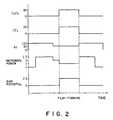
- Fig.2shows a sequence of processes.
- the Ar gasstarts to be introduced at a flow rate of 150 sccm at first.
- microwave power of 2.7 kWis supplied.
- the flow rate of the Ar gasis changed into 90 sccm and the microwave power starts to be decreased toward 1 kW step-by-step and/or gradually.
- the CF 4 gasstarts to be introduced at the flow rate of 40 sccm
- the C 6 F 6 gasstarts to be introduced at the flow rate of 20 sccm
- the bias power of 2.5 kWstarts to be supplied.
- the film-forming processis conducted for a predetermined time.
- the CF 4 gas and the C 6 F 6 gas stopbeing introduced, the bias power stops being supplied, the flow rate of the Ar gas is changed back into 150 sccm and the microwave power is changed back into 2.7 kW.
- the microwave power stopsbeing supplied and then the Ar gas stops being introduced, that is, the series of processes is completed.
- the CF 4 gas for etching the CF filmis added to the C 6 F 6 gas being the film-forming gas.
- the CF filmcan satisfactorily fill concave portions while less voids are generated. The reason may be guessed as follows.
- the C 6 F 6 gashas a benzene ring
- the molecule of the C 6 F 6 gasis large and the intra-molecular bonding-force thereof is strong.
- the C 6 F 6 gasis made into plasma while maintaining the large molecular state.
- the C 6 F 6 gaswhose molecule has a ringed structure and is large and whose intra-molecular bonding-force is strong, is gradually accumulated.
- the CF film 63can not be accumulated on both side surfaces of the small-frontage concave portions 64, but tends to be accumulated above the concave portions 64 in such a manner that shoulder-like portions of the accumulated film bulge out and block access to the concave portions 64 (see Fig.3).
- the C 6 F 6 gasis made into plasma together with the CF 4 gas in the vacuum container 2.
- the CF 4 gashas an etching function against the CF film, it may be guessed that strong intra-molecular bonding of the C 6 F 6 can be cut off because of the CF 4 gas. That is, F in the CF 4 made into plasma reacts with C in the C 6 F 6 to be a C-F gas, so that the C-C bonding of the C 6 F 6 is cut off.
- the intra-molecular bondingmay be cut off in the CF film formed by the C 6 F 6 or in the C 6 F 6 gas. If the bonding in the CF film is cut off, the molecule at the cut portion becomes small and the cut small molecule may be rebonded. Thus, it is guessed that the CF film 63 may be easily accumulated on the side surfaces of the concave portions 64. In addition, as shown in Fig.4, if the bonding in the C 6 F 6 gas is cut off, the ringed structure is broken down and the molecule becomes small. Thus, it is guessed that the small molecule may easily go into inside areas of the concave portions 64.
- the CF 4 gascan etch the CF film 63 itself.
- spatter-etchingis conducted by the CF 4 gas in such a manner that the shoulder-like portions of the film above the concave portions 64 between the wires 62, 62 are removed to enlarge the frontages of the concave portions 64.
- the CF film formed by the method of the inventionhas a high insulation performance, which is clearly shown by the experiments described below. The reason is guessed to be that the bonding of the C 6 F 6 is cut off by the added CF 4 gas and that F is rebonded to the cut-off portions to prevent electric current from flowing.
- the dielectric constantcan be more reduced by taking F into the CF film by means of rebonding of F.
- the CF film formed by the method of the inventioncan be used as an interlayer dielectric film very effectively.
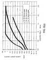
- Fig.6shows a graph of showing a relationship between flow rates of CF 4 gas and relative dielectric constants.
- the formed CF filmhas a high thermal stability.
- the high thermal stabilitymeans that even if the CF film is heated to a high temperature, an F(fluorine)-gas such as F, CF, or CF 2 tends not to break away from the CF film. If the F-gas tends not to break away from the CF film, corrosion of metal wires, undulating and/or cracking of the aluminum wires, rising of the relative dielectric constant and so on may be prevented.
- the reason why the thermal stability is high when the C 6 F 6 gas is used as the film-forming gasis guessed as follows.
- the benzene ringis stable because the A-state and the B-state resonate with each other and the C-C bonding is in an intermediate state between a single-bonding state and a double-bonding state.
- the C-C combination in the benzene ring included in the CF filmhas a strong bonding-force.
- bonding of C in the benzene ring and C outside the benzene ringhas a strong bonded-force as well.
- the CF or the CF 2are prevented from breaking away.
- the number of double-bondingis increased by recombination of the broken molecules in the CF film so that the film becomes dense.
- the thermal stability of the CF filmmay be more improved.
- a gas including Fsuch as C 2 F 6 gas, C 4 F 8 gas, C 5 F 8 gas, NF 3 gas or SiF 4 gas
- a gas including Osuch as O 2 gas, O 3 gas, CO gas or CO 2 gas
- a gas including Hsuch as H 2 gas, H 2 O gas, H 2 O 2 gas or NH 3 gas
- Fsuch as C 2 F 6 gas, C 4 F 8 gas, C 5 F 8 gas, NF 3 gas or SiF 4 gas
- a gas including Osuch as O 2 gas, O 3 gas, CO gas or CO 2 gas
- a gas including Hsuch as H 2 gas, H 2 O gas, H 2 O 2 gas or NH 3 gas
- the gas including Fis used, similarly to the CF 4 gas, F made into plasma reacts with C in the C 6 F 6 , so that the C 6 F 6 is broken and/or the CF film is etched.
- the gas including Ois used, O made into plasma reacts with C in the C 6 F 6 to be CO 2 gas, so that the C 6 F 6 is broken and/or the CF film is etched.
- the gas including HH made into plasma reacts with C in the C 6 F 6 or C in the CF film to be a C-H gas such as CH 4 or C 2 H 6 and fly away, so that the C 6 F 6 is broken and/or the CF film is etched.
- a CF film having a high insulation performance and a low dielectric constantmay be formed.
- a hydrocarbon gassuch as C 2 H 2 gas, C 2 H 4 gas or CH 4 gas, or a gas including silicon such as SiH 4 gas, Si 2 H 6 gas or SiF 4 gas may be added.
- a hydrocarbon gassuch as C 2 H 2 gas, C 2 H 4 gas or CH 4 gas, or a gas including silicon such as SiH 4 gas, Si 2 H 6 gas or SiF 4 gas may be added.
- the film-forming processwas conducted for 3 minutes and 15 seconds in order to form a CF film, while the C 6 F 6 gas is introduced at a flow rate of 40 sccm as a film-forming gas and the Ar gas is introduced at a flow rate of 30 sccm as a plasma gas (Comparison 1).
- the microwave power and the bias powerwere set 1 kW and 1.5 kW, respectively.
- the CF film formed by using O 2 gas as an etching gas and the CF film formed by using H 2 gas as an etching gaswere examined whether there were voids or not. Consequently, there were substantially no conspicuous voids in both of the films.
- the flow rate of the O 2 gaswas 10 sccm and the flow rate of the H 2 gas was 20 sccm.
- the other conditionswere kept the same as the example 1.
- the CF film formed by using CF 4 gas as an etching gas and by adding the C 2 H 2 gas and the CF film formed by using CF 4 gas as an etching gas and by adding the SiH 4 gaswere examined whether there were voids or not. Consequently, there were substantially no conspicuous voids in both of the films. That is, it was confirmed that even if these gases are added, the concave portions might be satisfactorily filled with the CF film.
- the thermal stabilitywas examined by means of a change in the weight between before and after an annealing process in the furnace, which change was measured by an electronic force balance. As a result, it was confirmed that the weight reduced by 1.7 %.
- the adhering forcewas examined by a stud-pull method (Sebastian method). As a result, it was confirmed that the adhering force was 7 kpsi. In the case, the flow rate of the C 2 H 2 gas was 10 sccm and the flow rate of the SiH 4 gas was 10 sccm. The other conditions were kept the same as the example 1.
- the insulation propertywas examined.
- the CF filmwas formed on a 8-inch wafer 10, while the C 6 F 6 gas is introduced at a flow rate of 40 sccm as a film-forming gas, the CF 4 gas is introduced at flow rates described below as an etching gas and the Ar gas is introduced at a flow rate of 90 sccm as a plasma gas.
- the microwave power and the bias powerwere set 1 kW and 2.5 kW, respectively. Samples obtained according to the above manner were subject to a changeable electric field, so that electric currents in the samples were measured.
- the flow rate of the CF 4 gaswas changed between 0 sccm and 20 sccm.
- the electric currentswere measured at a central position of the wafer 10 and at a peripheral position of the wafer 10 (a position inward from the peripheral edge by 13 mm).
- ⁇means that the flow rate of the CF 4 gas was 20 sccm and the measurement was conducted at the central position of the wafer 10.
- ⁇means that the flow rate of the CF 4 gas was 10 sccm and the measurement was conducted at the central position of the wafer 10.
- ⁇means that the flow rate of the CF 4 gas was 0 sccm and the measurement was conducted at the central position of the wafer 10.
- ⁇means that the flow rate of the CF 4 gas was 20 sccm and the measurement was conducted at the peripheral position of the wafer 10.
- ⁇means that the flow rate of the CF 4 gas was 10 sccm and the measurement was conducted at the peripheral position of the wafer 10.
- ⁇means that the flow rate of the CF 4 gas was 0 sccm and the measurement was conducted at the peripheral position of the wafer 10.
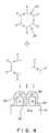
- the film-forming gas for the CF filmmay be a compound gas including a benzene ring such as octafluorotoluene or fluorobenzene.
- a compound gas of C and Fsuch as 1,4-bistrifluoromethylbenzene (C 6 H 4 (CF 3 ) 2 ) or perfluorotoluene gas (C 6 F 5 CF 3 ) may be used.
- this inventionis not limited by the manner of generating plasma by ECR.
- this inventionmay be applied to a case of generating plasma by a method called ICP (Inductive Coupled Plasma) wherein a coil wound around a dome-like container gives an electric field and a magnetic field to a process gas.
- ICPInductive Coupled Plasma
- This inventionmay also be applied to a case of generating plasma by an interaction of a helicon wave of for example 13.56 MHz and a magnetic field formed by a magnetic coil, which plasma is called helicon-wave plasma.
- This inventionmay also be applied to a case of generating plasma by applying a magnetic field to two parallel cathodes in a substantially parallel manner, which plasma is called magnetron plasma.
- This inventionmay also be applied to a case of generating plasma by applying a high-frequency electric power between electrodes facing with each other, which are called parallel-plates.
Landscapes
- Chemical & Material Sciences (AREA)
- Engineering & Computer Science (AREA)
- Chemical Kinetics & Catalysis (AREA)
- Physics & Mathematics (AREA)
- Manufacturing & Machinery (AREA)
- Microelectronics & Electronic Packaging (AREA)
- Power Engineering (AREA)
- Computer Hardware Design (AREA)
- General Physics & Mathematics (AREA)
- Condensed Matter Physics & Semiconductors (AREA)
- General Chemical & Material Sciences (AREA)
- Organic Chemistry (AREA)
- Metallurgy (AREA)
- Materials Engineering (AREA)
- Mechanical Engineering (AREA)
- Inorganic Chemistry (AREA)
- Plasma & Fusion (AREA)
- Drying Of Semiconductors (AREA)
Abstract
Description
This invention relates to a method for forming for examplean interlayer dielectric film of a semiconductor device, forexample a film of carbon added fluorine (fluorine-added carbon).
In order to integrate semiconductor devices in higherdensity, various ideas have been proposed, for example, makingpatterns minute or multilayering circuits. As one of the ideas,there is known an art for multilayering wires. In order to achievea multilayered wiring structure, an (n)-th wiring layer and an(n+1)-th wiring layer are connected with each other via anelectric conducting layer. In addition, a thin film, which iscalled an interlayer dielectric film, is formed at an area orareas except the electric conducting layer.
An SiO2 film is a typical interlayer dielectric film.However, recently, it is required to lower a dielectric constantof the interlayer dielectric film in order to raise a speed ofoperation of the device further more. Then, characteristics ofmaterials for the interlayer dielectric films are examined andstudied. The Sio2 has a dielectric constant of about 4. Thus,various efforts have been made to find or form a material havinga smaller dielectric constant. As one of the efforts, an SiOFfilm having a dielectric constant of 3.5 has been developed.However, inventors of this invention have paid attention to afilm of flurorine-added carbon (hereafter, which is abbreviatedas a CF film) having a further smaller dielectric constant.
Such a CF film is formed for example by using Argon (Ar)gas as a plasma gas, using a mixed gas including a compound gasof carbon (C) and fluorine (F) and a hydrocarbon gas as afilm-forming gas, and making the film-forming gas into plasmain a plasma unit which can generate plasma for example by usingelectron cyclotron resonance. Then, the inventors have examinedto use C6F6 (hexafluorobenzene) gas as the film-forming gas inorder to raise thermal stability of the CF film.
If the CF film is used as an interlayer dielectric film,for example as shown in Fig.10, aCF film 13 is accumulated ona SiO2 film 11 on whichaluminum wires 12 are formed, so that gapsbetween thewires CF film 13. However,if C6F6 gas is used as the film-forming gas, since the C6F6 gashas a benzene ring i.e. a molecule of the C6F6 is large, as shownin Fig.10 (a), shoulder-like portions of the accumulated filmabove both side edges of aconcave portion 14 between thewires CF film 13 is accumulated. Then, theshoulder-like portions may contact with each other to block accessto theconcave portion 14. Thus, even if theconcave portion 14has an aspect ratio that is not so large, theconcave portion 14 can not be filled with theCF film 13. That is, a or more largevoids (spaces) 15 may be formed in the portion (see Fig.10 (b)).
This invention is intended to solve the above problem.The object of this invention is to provide a plasma film-formingmethod which can satisfactory fill up a concave portion with aCF film.
In order to achieve the object, a plasma film-formingmethod (a method of plasma-assisted film deposition) has a featureof comprising: a plasma-making step of making into plasma afilm-forming gas including a compound of carbon and fluorine andan etching gas which can etch a film of fluorine-added carbon;and a film-forming step of forming a film of fluorine-added carbononto an object to be processed by means of the plasma made inthe plasma-making step.
According to the feature, if the CF film is used as aninterlayer dielectric film, since the etching gas for etchingthe CF film is supplied in addition to the film-forming gas, aconcave portion can be satisfactory filled up with the CF film.
The film-forming gas including a compound of carbon andfluorine includes for example a gas of a compound having a benzenering, in particular hexafluorobenzene.
Preferably, the etching gas which can etch a film offluorine-added carbon is a gas including fluorine, a gas includingoxygen or a gas including hydrogen.
Preferably, hydrocarbon gas or a gas including silicon issupplied in addition to the film-forming gas and the etching gas,in the plasma-making step.
At first, an example of a plasma film-forming unit usedin an embodiment according to the invention is shown in Fig.1.The unit includes avacuum container 2 made of for example aluminumor the like. Thevacuum container 2 includes a firstcylindricalvacuum chamber 21 located in an upper portion thereof forgenerating plasma, and a secondcylindrical vacuum chamber 22having a diameter larger than that of thefirst vacuum chamber 21. Thesecond vacuum chamber 22 is arranged under and connectedto thefirst vacuum chamber 21. In addition, thevacuum container 2 is grounded to be in zero potential.
An upper end of thevacuum container 2 has an opening. Apenetrable window 23 made of a microwave penetrable material suchas a crystal is sealingly fitted in the opening. Thus, an insideof thevacuum container 2 can be maintained at a vacuum. Awaveguide 25 is provided outside of thepenetrable window 23. Thewave guide 25 is connected to a high-frequency power source 24,which can generate a microwave of for example 2.45 GHz. Then,the microwave generated by the high-frequency power source 24is introduced via thewave guide 25 by for example a TE mode.Alternatively, the microwave guided by the TE mode is convertedto a TM mode in thewave guide 25, and the converted microwavecan be introduced into thefirst vacuum chamber 21 through thepenetrable window 23.
A plurality ofgas nozzles 31 are arranged around a sidewall defining thefirst vacuum chamber 21, for example atsubstantially regular intervals in a peripheral directionthereof. The plurality ofgas nozzles 31 are connected to a gassource such as a plasma-generating gas source not shown. Thus,a plasma-generating gas such as Ar gas can be uniformly suppliedinto an upper portion of thefirst vacuum chamber 21.
Astage 4 for a semiconductor wafer 10 (hereafter, whichis abbreviated as a wafer) is arranged in thesecond vacuum chamber 22 to face thefirst vacuum chamber 21. Thestage 4 has anelectrostatic chuck 41 in a surface portion thereof. Electrodesof theelectrostatic chuck 41 are connected to a direct-currentpower source (not shown) for sticking to the wafer and to ahigh-frequency power source 42 for applying a bias electric power(bias-potential) to draw ions up to the wafer.
A circular film-forming-gas supplying member 5 is providedat an upper portion of thesecond vacuum chamber 22, that is,at a connecting portion of thesecond vacuum chamber 22 and thefirst vacuum chamber 21. For example, a firm-forming gas issupplied from a gas-supplyingtube 51 and an etching gas addedto the film-forming gas is supplied from a gas-supplyingtube 52 into the film-forming-gas supplying member 5, respectively.Then, the film-forming-gas supplying member 5 is adapted to supplythese gases into thevacuum container 2 viagas holes 53 whichare formed in an inside surface thereof.
A magnetic-field forming means such as a circular mainelectromagnetic coil 26 is arranged around and near to the sidewall defining thefirst vacuum chamber 21. A circular auxiliaryelectromagnetic coil 27 is arranged below thesecond vacuumchamber 22.Exhausting pipes 28 are connected to a base plateof thesecond vacuum chamber 22, for example at two positionssymmetric with respect to a central axis of thevacuum chamber 22.
Then, a method of the invention carried out by using theabove unit is explained with reference to Figs.3 and 4. In thecase, aCF film 63 is formed as an interlayer dielectric filmon a SiO2 film 61 which is formed on awafer 10 and on whichaluminumwires
In detail, at first, a gate valve (not shown) provided ata side wall of thevacuum container 2 is opened. A conveying arm(not shown) conveys thewafer 10, on whose surface the aluminumwires are formed, from a load-lock chamber (not shown) onto thestage 4 via the gate valve. Thewafer 10 conveyed onto thestage 4 is electrostaticly adhered to theelectrostatic chuck 41. Then,theCF film 63 is formed on the surface of the SiO2 film 61.
That is, the gate valve is closed, and the inside of thevacuum container 2 is hermetically closed. Then, gas of theinside of thevacuum container 2 is exhausted from theexhaustingpipes 28, so that the inside of thevacuum container 2 is producedto a predetermined vacuum and maintained at a predeterminedprocess pressure. In such a state, a plasma-generating gas suchas Ar gas is introduced into thefirst vacuum chamber 21 throughthegas nozzles 31 at a flow rate of for example 90 sccm. At thesame time, a film-forming gas including a compound of carbon andfluorine and including a benzene ring such as C6F6 gas and anetching gas capable of etching a CF film such as CF4 gas areintroduced from the film-forminggas supplying member 5 into thesecond vacuum chamber 22 at respective flow rates of for example 40 sccm and 20 sccm, respectively. Then, the high-frequency wave(microwave) of 2.45 GHz and 1 kW is supplied by the high-frequencypower source 24, and a bias voltage of 13.56 MHz and 2.5 kW isapplied to thestage 4 by the high-frequency power source 42.
Thus, the microwave from the high-frequency power source 24 is introduced into thefirst vacuum chamber 21 through thewave guide 25 and through thepenetrable window 23 at the ceilingof thevacuum container 2. In thevacuum container 2, the mainelectromagnetic coil 26 and the auxiliary electromagnetic 27 forma magnetic field in a direction from an upper portion of thefirstvacuum chamber 21 toward a lower portion of thesecond vacuumchamber 22. For example, a strength of the magnetic field ata lower portion of thefirst vacuum chamber 21 is 875 gauss.
An electric cyclotron resonance is generated by aninteraction between the magnetic field and the microwave. Theresonance causes the Ar gas to become plasma and to be much dense.Since the plasma is made of Ar gas, the plasma is much stable.
The plasma flows from thefirst vacuum chamber 21 into thesecond vacuum chamber 22 and activates (makes into plasma) theC6F6 gas and the CF4 gas, which are supplied thereinto, to produceactivated species (plasma).
Ar ions, that are plasma ions, are drawn toward thewafer 10 by the bias electric potential for drawing the plasma. Then,the spatter-etching effect of the Ar ions cut off edges of theCF film accumulated on a pattern (concave portion) of the surfaceof thewafer 10 in order to enlarge an opening for access to theconcave portion. Thus, the CF film is formed and fills up theconcave portion.
In a case of manufacturing actual devices, after that, theCF film may be etched with a predetermined pattern. For example,W films may fill concave portions to form circuits of W.
Fig.2 shows a sequence of processes. As shown in Fig.2,in the actual processes, the Ar gas starts to be introduced ata flow rate of 150 sccm at first. Then, microwave power of 2.7kW is supplied. After a predetermined time has passed, the flowrate of the Ar gas is changed into 90 sccm and the microwave powerstarts to be decreased toward 1 kW step-by-step and/or gradually. When the microwave power is decreased to 1 kW, at the same time,the CF4 gas starts to be introduced at the flow rate of 40 sccm,the C6F6 gas starts to be introduced at the flow rate of 20 sccmand the bias power of 2.5 kW starts to be supplied. After that,the film-forming process is conducted for a predetermined time.
Then, the CF4 gas and the C6F6 gas stop being introduced,the bias power stops being supplied, the flow rate of the Ar gasis changed back into 150 sccm and the microwave power is changedback into 2.7 kW. Thus, the film-forming process is completed.Then, after a predetermined time has passed, the microwave powerstops being supplied and then the Ar gas stops being introduced,that is, the series of processes is completed.
In the invention, the CF4 gas for etching the CF film isadded to the C6F6 gas being the film-forming gas. Thus, as clearlyshown by experiments described below, the CF film cansatisfactorily fill concave portions while less voids aregenerated. The reason may be guessed as follows.
As shown in Fig.3, since the C6F6 gas has a benzene ring,the molecule of the C6F6 gas is large and the intra-molecularbonding-force thereof is strong. Thus, when only the C6F6 gas isused for forming theCF film 63 onto the SiO2 film 61 which hasan aluminum pattern makingconcave portions 64 each of that hasa width of for example about 0.3µm, the C6F6 gas is made intoplasma while maintaining the large molecular state. Thus, it maybe difficult for the C6F6 gas to go into inside areas of theconcaveportions 64.
In addition, the C6F6 gas, whose molecule has a ringedstructure and is large and whose intra-molecular bonding-forceis strong, is gradually accumulated. Thus, theCF film 63 cannot be accumulated on both side surfaces of the small-frontageconcave portions 64, but tends to be accumulated above theconcaveportions 64 in such a manner that shoulder-like portions of theaccumulated film bulge out and block access to the concaveportions 64 (see Fig.3). Thus, it may be more difficult for theC6F6 gas to go into theconcave portions 64. As a result, it maybe guessed that the portions tend to be large voids.
On the other hand, if the CF4 gas is added to the C6F6 gas, the C6F6 gas is made into plasma together with the CF4 gas in thevacuum container 2. As the CF4 gas has an etching function againstthe CF film, it may be guessed that strong intra-molecular bondingof the C6F6 can be cut off because of the CF4 gas. That is, F inthe CF4 made into plasma reacts with C in the C6F6 to be a C-F gas,so that the C-C bonding of the C6F6 is cut off.
It is guessed that the intra-molecular bonding may be cutoff in the CF film formed by the C6F6 or in the C6F6 gas. If thebonding in the CF film is cut off, the molecule at the cut portionbecomes small and the cut small molecule may be rebonded. Thus,it is guessed that theCF film 63 may be easily accumulated onthe side surfaces of theconcave portions 64. In addition, asshown in Fig.4, if the bonding in the C6F6 gas is cut off, theringed structure is broken down and the molecule becomes small.Thus, it is guessed that the small molecule may easily go intoinside areas of theconcave portions 64.
In addition, the CF4 gas can etch theCF film 63 itself.Thus, it is guessed that as shown in Fig.5, while the CF filmis formed by the C6F6 gas, spatter-etching is conducted by theCF4 gas in such a manner that the shoulder-like portions of thefilm above theconcave portions 64 between thewires concave portions 64.
Thus, during the film-forming process, broken componentsof the C6F6 go into theconcave portions 64 through the frontagesthereof enlarged by cutting off the bonding of theCF film 63and/or by spatter-etching theCF film 63. Thus, the CF film tendsto be accumulated on bottom areas of theconcave portions 64.As a result, theconcave portions 64 can be filled up while lessvoids are formed. In addition, it is guessed that degree ofbreaking down the molecules of the C6F6 gas may be adjusted byan amount of the added etching gas.
In addition, the CF film formed by the method of theinvention has a high insulation performance, which is clearlyshown by the experiments described below. The reason is guessedto be that the bonding of the C6F6 is cut off by the added CF4 gasand that F is rebonded to the cut-off portions to prevent electriccurrent from flowing. In addition, the dielectric constant can be more reduced by taking F into the CF film by means of rebondingof F. Thus, the CF film formed by the method of the inventioncan be used as an interlayer dielectric film very effectively.Fig.6 shows a graph of showing a relationship between flow ratesof CF4 gas and relative dielectric constants.
In addition, since the C6F6 gas is used as the film-forminggas in the above process, the formed CF film has a high thermalstability. Herein, the high thermal stability means that evenif the CF film is heated to a high temperature, an F(fluorine)-gassuch as F, CF, or CF2 tends not to break away from the CF film.If the F-gas tends not to break away from the CF film, corrosionof metal wires, undulating and/or cracking of the aluminum wires,rising of the relative dielectric constant and so on may beprevented.
As described above, the reason why the thermal stabilityis high when the C6F6 gas is used as the film-forming gas is guessedas follows. As shown in Fig. 7, the benzene ring is stable becausethe A-state and the B-state resonate with each other and the C-Cbonding is in an intermediate state between a single-bonding stateand a double-bonding state. Thus, the C-C combination in thebenzene ring included in the CF film has a strong bonding-force.In addition, it is guessed that bonding of C in the benzene ringand C outside the benzene ring has a strong bonded-force as well.Thus, it is guessed that the CF or the CF2 are prevented frombreaking away. In addition, in the invention, the number ofdouble-bonding is increased by recombination of the brokenmolecules in the CF film so that the film becomes dense. Thus,the thermal stability of the CF film may be more improved.
In the above process, a gas including F such as C2F6 gas,C4F8 gas, C5F8 gas, NF3 gas or SiF4 gas, a gas including O such asO2 gas, O3 gas, CO gas or CO2 gas, or a gas including H such asH2 gas, H2O gas, H2O2 gas or NH3 gas may be used as the etchinggas for etching the CF film, instead of the CF4 gas.
If the gas including F is used, similarly to the CF4 gas,F made into plasma reacts with C in the C6F6, so that the C6F6 isbroken and/or the CF film is etched. If the gas including O isused, O made into plasma reacts with C in the C6F6 to be CO2 gas, so that the C6F6 is broken and/or the CF film is etched. In addition,if the gas including H is used, H made into plasma reacts withC in the C6F6 or C in the CF film to be a C-H gas such as CH4 orC2H6 and fly away, so that the C6F6 is broken and/or the CF filmis etched.
If the gas including O is used, since C is carried awayby O, density of F in the film is raised. If the gas includingH is used, since C is carried away as a C-H gas, density of Fin the film is raised.
As described above, even if the gas including F, the gasincluding O or the gas including H is used as the etching gasinstead of the CF4 gas, a CF film having a high insulationperformance and a low dielectric constant may be formed.
In addition, in the invention, after the etching gas isadded to the film-forming gas, a hydrocarbon gas such as C2H2 gas,C2H4 gas or CH4 gas, or a gas including silicon such as SiH4 gas,Si2H6 gas or SiF4 gas may be added. In the case, since densityof C and/or Si in the CF film may be raised, the thermal stabilityand/or the adhering property of the formed CF film may be improved.
Next, experiments conducted for confirming effects of theinvention are explained. In the experiments, the plasmaprocessing unit as shown in Fig.1 was used. Each of theexperiments was conducted to awafer 10 on which wires had beenformed in such a manner that each gap between two adjacent wireshas an aspect ratio of 3. The film-forming process was conductedfor 4 minutes and 40 seconds in order to form a CF film, whilethe C6F6 gas is introduced at a flow rate of 40 sccm as afilm-forming gas, the CF4 gas is introduced at a flow rate of 20sccm as an etching gas and the Ar gas is introduced at a flowrate of 90 sccm as a plasma gas. In the case, the process wasconducted according to the sequence shown in Fig.2, while themicrowave power and the bias power were set 1 kW and 2.5 kW,respectively (Example 1).
In addition, as a comparison, by using the plasmaprocessing unit as shown in Fig.1, the film-forming process wasconducted for 3 minutes and 15 seconds in order to form a CF film,while the C6F6 gas is introduced at a flow rate of 40 sccm as a film-forming gas and the Ar gas is introduced at a flow rate of30 sccm as a plasma gas (Comparison 1). In the case, the microwavepower and the bias power were set 1 kW and 1.5 kW, respectively.
The CF film by the example 1 described above and the CFfilm by thecomparison 1 described above were examined whetherthere were voids or not by a SEM (Scanning Electron Microscope).Consequently, as shown in Fig.8(a), there were substantially noconspicuous voids in theconcave portions 64 between thewires large voids 65 having a size of about0.7µm X 0.3µm in the CF film of thecomparison 1, because theCF film 63 was hardly accumulated on the side surfaces of thewires 62, although theCF film 63 was slightly accumulated onthe bottom areas in theconcave portions 64 between thewires
Similarly to the example 1, the CF film formed by usingO2 gas as an etching gas and the CF film formed by using H2 gasas an etching gas were examined whether there were voids or not.Consequently, there were substantially no conspicuous voids inboth of the films. In the case, the flow rate of the O2 gas was10 sccm and the flow rate of the H2 gas was 20 sccm. The otherconditions were kept the same as the example 1.
In addition, similarly to the example 1, the CF film formedby using CF4 gas as an etching gas and by adding the C2H2 gas andthe CF film formed by using CF4 gas as an etching gas and by addingthe SiH4 gas were examined whether there were voids or not.Consequently, there were substantially no conspicuous voids inboth of the films. That is, it was confirmed that even if thesegases are added, the concave portions might be satisfactorilyfilled with the CF film.
In addition, the thermal stability was examined by meansof a change in the weight between before and after an annealingprocess in the furnace, which change was measured by an electronicforce balance. As a result, it was confirmed that the weight reduced by 1.7 %. In addition, the adhering force was examinedby a stud-pull method (Sebastian method). As a result, it wasconfirmed that the adhering force was 7 kpsi. In the case, theflow rate of the C2H2 gas was 10 sccm and the flow rate of theSiH4 gas was 10 sccm. The other conditions were kept the sameas the example 1.
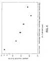
In addition, with respect to the CF film formed by themethod of the invention, the insulation property was examined.By using the plasma processing unit as shown in Fig.1, the CFfilm was formed on a 8-inch wafer 10, while the C6F6 gas isintroduced at a flow rate of 40 sccm as a film-forming gas, theCF4 gas is introduced at flow rates described below as an etchinggas and the Ar gas is introduced at a flow rate of 90 sccm asa plasma gas. In the case, the microwave power and the bias powerwere set 1 kW and 2.5 kW, respectively. Samples obtainedaccording to the above manner were subject to a changeableelectric field, so that electric currents in the samples weremeasured. The flow rate of the CF4 gas was changed between 0 sccmand 20 sccm. The electric currents were measured at a centralposition of thewafer 10 and at a peripheral position of the wafer10 (a position inward from the peripheral edge by 13 mm).
The results are shown in Fig.9(a)(b). In Fig.9(a)(b), theabscissa represents the electric field and the ordinaterepresents the electric-current density, respectively. ▪ meansthat the flow rate of the CF4 gas was 20 sccm and the measurementwas conducted at the central position of thewafer 10. meansthat the flow rate of the CF4 gas was 10 sccm and the measurementwas conducted at the central position of thewafer 10. ▴ meansthat the flow rate of the CF4 gas was 0 sccm and the measurementwas conducted at the central position of thewafer 10. □ meansthat the flow rate of the CF4 gas was 20 sccm and the measurementwas conducted at the peripheral position of thewafer 10. ○ meansthat the flow rate of the CF4 gas was 10 sccm and the measurementwas conducted at the peripheral position of thewafer 10. Δ meansthat the flow rate of the CF4 gas was 0 sccm and the measurementwas conducted at the peripheral position of thewafer 10.
As shown in Fig.9(a)(b), the electric current was larger when the CF4 gas was not added than when the CF4 gas was added.That is, it was confirmed that the insulation property was raisedby adding the CF4 gas.
In the invention, the film-forming gas for the CF film maybe a compound gas including a benzene ring such asoctafluorotoluene or fluorobenzene. In addition, a compound gasof C and F such as 1,4-bistrifluoromethylbenzene (C6H4(CF3)2) orperfluorotoluene gas (C6F5CF3) may be used.
In addition, this invention is not limited by the mannerof generating plasma by ECR. For example, this invention maybe applied to a case of generating plasma by a method called ICP(Inductive Coupled Plasma) wherein a coil wound around a dome-likecontainer gives an electric field and a magnetic field to a processgas. This invention may also be applied to a case of generatingplasma by an interaction of a helicon wave of for example 13.56MHz and a magnetic field formed by a magnetic coil, which plasmais called helicon-wave plasma. This invention may also beapplied to a case of generating plasma by applying a magneticfield to two parallel cathodes in a substantially parallel manner,which plasma is called magnetron plasma. This invention may alsobe applied to a case of generating plasma by applying ahigh-frequency electric power between electrodes facing witheach other, which are called parallel-plates.
Claims (14)
- A plasma film-forming method comprising;a plasma-making step of making into plasma a film-forminggas including a compound of carbon and fluorine and an etchinggas which can etch a film of fluorine-added carbon, anda film-forming step of forming a film of fluorine-addedcarbon onto an object to be processed by means of the plasma madein the plasma-making step.
- A plasma film-forming method according to claim 1, wherein:
the film-forming gas including a compound of carbon andfluorine includes a gas of a compound having a benzene ring. - A plasma film-forming method according to claim 2, wherein:
the film-forming gas including a compound of carbon andfluorine includes hexafluorobenzene. - A plasma film-forming method according to claim 1, wherein:
the etching gas which can etch a film of fluorine-addedcarbon is a gas including fluorine. - A plasma film-forming method according to claim 2, wherein:
the etching gas which can etch a film of fluorine-addedcarbon is a gas including fluorine. - A plasma film-forming method according to claim 3, wherein:
the etching gas which can etch a film of fluorine-addedcarbon is a gas including fluorine. - A plasma film-forming method according to claim 1, wherein:
the etching gas which can etch a film of fluorine-addedcarbon is a gas including hydrogen. - A plasma film-forming method according to claim 2, wherein:
the etching gas which can etch a film of fluorine-addedcarbon is a gas including hydrogen. - A plasma film-forming method according to claim 3, wherein:
the etching gas which can etch a film of fluorine-addedcarbon is a gas including hydrogen. - A plasma film-forming method according to claim 1, wherein:
the etching gas which can etch a film of fluorine-addedcarbon is a gas including oxygen. - A plasma film-forming method according to claim 2, wherein:
the etching gas which can etch a film of fluorine-added carbon is a gas including oxygen. - A plasma film-forming method according to claim 3, wherein:
the etching gas which can etch a film of fluorine-addedcarbon is a gas including oxygen. - A plasma film-forming method according to claim 1, wherein:
a hydrocarbon gas is supplied in addition to the film-forminggas and the etching gas in the plasma-making step. - A plasma film-forming method according to claim 1, wherein:
a gas including silicon is supplied in addition to thefilm-forming gas and the etching gas in the plasma-making step.
Applications Claiming Priority (3)
| Application Number | Priority Date | Filing Date | Title |
|---|---|---|---|
| JP29003798 | 1998-09-28 | ||
| JP29003798 | 1998-09-28 | ||
| PCT/JP1999/005203WO2000019507A1 (en) | 1998-09-28 | 1999-09-22 | Method of plasma-assisted film deposition |
Publications (2)
| Publication Number | Publication Date |
|---|---|
| EP1119034A1true EP1119034A1 (en) | 2001-07-25 |
| EP1119034A4 EP1119034A4 (en) | 2002-12-04 |
Family
ID=17750976
Family Applications (1)
| Application Number | Title | Priority Date | Filing Date |
|---|---|---|---|
| EP99944797AWithdrawnEP1119034A4 (en) | 1998-09-28 | 1999-09-22 | FILM DEPOSIT ASSISTED BY PLASMA |
Country Status (5)
| Country | Link |
|---|---|
| US (1) | US6576569B1 (en) |
| EP (1) | EP1119034A4 (en) |
| KR (1) | KR100430807B1 (en) |
| TW (1) | TW429427B (en) |
| WO (1) | WO2000019507A1 (en) |
Cited By (21)
| Publication number | Priority date | Publication date | Assignee | Title |
|---|---|---|---|---|
| WO2004001832A1 (en)* | 2002-06-21 | 2003-12-31 | E.I. Du Pont De Nemours And Company | Fluoropolymer interlayer dielectric by chemical vapor deposition |
| WO2004105114A1 (en) | 2003-05-22 | 2004-12-02 | Tokyo Electron Limited | Method of forming fluorinated carbon film |
| US9272095B2 (en) | 2011-04-01 | 2016-03-01 | Sio2 Medical Products, Inc. | Vessels, contact surfaces, and coating and inspection apparatus and methods |
| US9458536B2 (en) | 2009-07-02 | 2016-10-04 | Sio2 Medical Products, Inc. | PECVD coating methods for capped syringes, cartridges and other articles |
| US9545360B2 (en) | 2009-05-13 | 2017-01-17 | Sio2 Medical Products, Inc. | Saccharide protective coating for pharmaceutical package |
| US9554968B2 (en) | 2013-03-11 | 2017-01-31 | Sio2 Medical Products, Inc. | Trilayer coated pharmaceutical packaging |
| US9572526B2 (en) | 2009-05-13 | 2017-02-21 | Sio2 Medical Products, Inc. | Apparatus and method for transporting a vessel to and from a PECVD processing station |
| US9664626B2 (en) | 2012-11-01 | 2017-05-30 | Sio2 Medical Products, Inc. | Coating inspection method |
| US9662450B2 (en) | 2013-03-01 | 2017-05-30 | Sio2 Medical Products, Inc. | Plasma or CVD pre-treatment for lubricated pharmaceutical package, coating process and apparatus |
| US9764093B2 (en) | 2012-11-30 | 2017-09-19 | Sio2 Medical Products, Inc. | Controlling the uniformity of PECVD deposition |
| US9863042B2 (en) | 2013-03-15 | 2018-01-09 | Sio2 Medical Products, Inc. | PECVD lubricity vessel coating, coating process and apparatus providing different power levels in two phases |
| US9878101B2 (en) | 2010-11-12 | 2018-01-30 | Sio2 Medical Products, Inc. | Cyclic olefin polymer vessels and vessel coating methods |
| US9903782B2 (en) | 2012-11-16 | 2018-02-27 | Sio2 Medical Products, Inc. | Method and apparatus for detecting rapid barrier coating integrity characteristics |
| US9937099B2 (en) | 2013-03-11 | 2018-04-10 | Sio2 Medical Products, Inc. | Trilayer coated pharmaceutical packaging with low oxygen transmission rate |
| US10189603B2 (en) | 2011-11-11 | 2019-01-29 | Sio2 Medical Products, Inc. | Passivation, pH protective or lubricity coating for pharmaceutical package, coating process and apparatus |
| US10201660B2 (en) | 2012-11-30 | 2019-02-12 | Sio2 Medical Products, Inc. | Controlling the uniformity of PECVD deposition on medical syringes, cartridges, and the like |
| US11066745B2 (en) | 2014-03-28 | 2021-07-20 | Sio2 Medical Products, Inc. | Antistatic coatings for plastic vessels |
| US11077233B2 (en) | 2015-08-18 | 2021-08-03 | Sio2 Medical Products, Inc. | Pharmaceutical and other packaging with low oxygen transmission rate |
| US11116695B2 (en) | 2011-11-11 | 2021-09-14 | Sio2 Medical Products, Inc. | Blood sample collection tube |
| US11624115B2 (en) | 2010-05-12 | 2023-04-11 | Sio2 Medical Products, Inc. | Syringe with PECVD lubrication |
| US12257371B2 (en) | 2012-07-03 | 2025-03-25 | Sio2 Medical Products, Llc | SiOx barrier for pharmaceutical package and coating process |
Families Citing this family (2)
| Publication number | Priority date | Publication date | Assignee | Title |
|---|---|---|---|---|
| KR100733440B1 (en)* | 2003-05-22 | 2007-06-29 | 동경 엘렉트론 주식회사 | Method of forming fluorinated carbon film |
| US20080038462A1 (en)* | 2006-08-09 | 2008-02-14 | Qimonda Ag | Method of forming a carbon layer on a substrate |
Family Cites Families (9)
| Publication number | Priority date | Publication date | Assignee | Title |
|---|---|---|---|---|
| US5238705A (en)* | 1987-02-24 | 1993-08-24 | Semiconductor Energy Laboratory Co., Ltd. | Carbonaceous protective films and method of depositing the same |
| JPH06101462B2 (en)* | 1991-04-30 | 1994-12-12 | インターナショナル・ビジネス・マシーンズ・コーポレイション | Method and substrate for bonding fluorocarbon polymer film to substrate |
| CA2157257C (en)* | 1994-09-12 | 1999-08-10 | Kazuhiko Endo | Semiconductor device with amorphous carbon layer and method of fabricating the same |
| JP2748879B2 (en)* | 1995-02-23 | 1998-05-13 | 日本電気株式会社 | Method for producing fluorinated amorphous carbon film material |
| US5462784A (en)* | 1994-11-02 | 1995-10-31 | International Business Machines Corporation | Fluorinated diamond-like carbon protective coating for magnetic recording media devices |
| US5942328A (en)* | 1996-02-29 | 1999-08-24 | International Business Machines Corporation | Low dielectric constant amorphous fluorinated carbon and method of preparation |
| JP2850834B2 (en)* | 1996-03-07 | 1999-01-27 | 日本電気株式会社 | Method for manufacturing amorphous carbon film and semiconductor device |
| JP3402972B2 (en)* | 1996-11-14 | 2003-05-06 | 東京エレクトロン株式会社 | Method for manufacturing semiconductor device |
| US6184572B1 (en)* | 1998-04-29 | 2001-02-06 | Novellus Systems, Inc. | Interlevel dielectric stack containing plasma deposited fluorinated amorphous carbon films for semiconductor devices |
- 1999
- 1999-09-22KRKR10-2001-7003730Apatent/KR100430807B1/ennot_activeExpired - Fee Related
- 1999-09-22WOPCT/JP1999/005203patent/WO2000019507A1/ennot_activeApplication Discontinuation
- 1999-09-22EPEP99944797Apatent/EP1119034A4/ennot_activeWithdrawn
- 1999-09-27TWTW088116519Apatent/TW429427B/ennot_activeIP Right Cessation
- 2000
- 2000-09-07USUS09/657,053patent/US6576569B1/ennot_activeExpired - Fee Related
Cited By (40)
| Publication number | Priority date | Publication date | Assignee | Title |
|---|---|---|---|---|
| WO2004001832A1 (en)* | 2002-06-21 | 2003-12-31 | E.I. Du Pont De Nemours And Company | Fluoropolymer interlayer dielectric by chemical vapor deposition |
| CN100336184C (en)* | 2002-06-21 | 2007-09-05 | 纳幕尔杜邦公司 | Fluoropolymer interlayer dielectric by chemical vapor deposition |
| WO2004105114A1 (en) | 2003-05-22 | 2004-12-02 | Tokyo Electron Limited | Method of forming fluorinated carbon film |
| EP1626439A4 (en)* | 2003-05-22 | 2008-04-16 | Tadahiro Ohmi | PROCESS FOR FORMING FLUORINATED CARBON FILM |
| US7538012B2 (en) | 2003-05-22 | 2009-05-26 | Tadahiro Ohmi | Fluorine-containing carbon film forming method |
| US9572526B2 (en) | 2009-05-13 | 2017-02-21 | Sio2 Medical Products, Inc. | Apparatus and method for transporting a vessel to and from a PECVD processing station |
| US9545360B2 (en) | 2009-05-13 | 2017-01-17 | Sio2 Medical Products, Inc. | Saccharide protective coating for pharmaceutical package |
| US10537273B2 (en) | 2009-05-13 | 2020-01-21 | Sio2 Medical Products, Inc. | Syringe with PECVD lubricity layer |
| US10390744B2 (en) | 2009-05-13 | 2019-08-27 | Sio2 Medical Products, Inc. | Syringe with PECVD lubricity layer, apparatus and method for transporting a vessel to and from a PECVD processing station, and double wall plastic vessel |
| US9458536B2 (en) | 2009-07-02 | 2016-10-04 | Sio2 Medical Products, Inc. | PECVD coating methods for capped syringes, cartridges and other articles |
| US11624115B2 (en) | 2010-05-12 | 2023-04-11 | Sio2 Medical Products, Inc. | Syringe with PECVD lubrication |
| US11123491B2 (en) | 2010-11-12 | 2021-09-21 | Sio2 Medical Products, Inc. | Cyclic olefin polymer vessels and vessel coating methods |
| US9878101B2 (en) | 2010-11-12 | 2018-01-30 | Sio2 Medical Products, Inc. | Cyclic olefin polymer vessels and vessel coating methods |
| US9272095B2 (en) | 2011-04-01 | 2016-03-01 | Sio2 Medical Products, Inc. | Vessels, contact surfaces, and coating and inspection apparatus and methods |
| US11724860B2 (en) | 2011-11-11 | 2023-08-15 | Sio2 Medical Products, Inc. | Passivation, pH protective or lubricity coating for pharmaceutical package, coating process and apparatus |
| US11148856B2 (en) | 2011-11-11 | 2021-10-19 | Sio2 Medical Products, Inc. | Passivation, pH protective or lubricity coating for pharmaceutical package, coating process and apparatus |
| US11884446B2 (en) | 2011-11-11 | 2024-01-30 | Sio2 Medical Products, Inc. | Passivation, pH protective or lubricity coating for pharmaceutical package, coating process and apparatus |
| US11116695B2 (en) | 2011-11-11 | 2021-09-14 | Sio2 Medical Products, Inc. | Blood sample collection tube |
| US10189603B2 (en) | 2011-11-11 | 2019-01-29 | Sio2 Medical Products, Inc. | Passivation, pH protective or lubricity coating for pharmaceutical package, coating process and apparatus |
| US10577154B2 (en) | 2011-11-11 | 2020-03-03 | Sio2 Medical Products, Inc. | Passivation, pH protective or lubricity coating for pharmaceutical package, coating process and apparatus |
| US12257371B2 (en) | 2012-07-03 | 2025-03-25 | Sio2 Medical Products, Llc | SiOx barrier for pharmaceutical package and coating process |
| US9664626B2 (en) | 2012-11-01 | 2017-05-30 | Sio2 Medical Products, Inc. | Coating inspection method |
| US9903782B2 (en) | 2012-11-16 | 2018-02-27 | Sio2 Medical Products, Inc. | Method and apparatus for detecting rapid barrier coating integrity characteristics |
| US9764093B2 (en) | 2012-11-30 | 2017-09-19 | Sio2 Medical Products, Inc. | Controlling the uniformity of PECVD deposition |
| US10201660B2 (en) | 2012-11-30 | 2019-02-12 | Sio2 Medical Products, Inc. | Controlling the uniformity of PECVD deposition on medical syringes, cartridges, and the like |
| US10363370B2 (en) | 2012-11-30 | 2019-07-30 | Sio2 Medical Products, Inc. | Controlling the uniformity of PECVD deposition |
| US11406765B2 (en) | 2012-11-30 | 2022-08-09 | Sio2 Medical Products, Inc. | Controlling the uniformity of PECVD deposition |
| US9662450B2 (en) | 2013-03-01 | 2017-05-30 | Sio2 Medical Products, Inc. | Plasma or CVD pre-treatment for lubricated pharmaceutical package, coating process and apparatus |
| US10016338B2 (en) | 2013-03-11 | 2018-07-10 | Sio2 Medical Products, Inc. | Trilayer coated pharmaceutical packaging |
| US9937099B2 (en) | 2013-03-11 | 2018-04-10 | Sio2 Medical Products, Inc. | Trilayer coated pharmaceutical packaging with low oxygen transmission rate |
| US12239606B2 (en) | 2013-03-11 | 2025-03-04 | Sio2 Medical Products, Llc | PECVD coated pharmaceutical packaging |
| US11298293B2 (en) | 2013-03-11 | 2022-04-12 | Sio2 Medical Products, Inc. | PECVD coated pharmaceutical packaging |
| US11344473B2 (en) | 2013-03-11 | 2022-05-31 | SiO2Medical Products, Inc. | Coated packaging |
| US9554968B2 (en) | 2013-03-11 | 2017-01-31 | Sio2 Medical Products, Inc. | Trilayer coated pharmaceutical packaging |
| US10912714B2 (en) | 2013-03-11 | 2021-02-09 | Sio2 Medical Products, Inc. | PECVD coated pharmaceutical packaging |
| US11684546B2 (en) | 2013-03-11 | 2023-06-27 | Sio2 Medical Products, Inc. | PECVD coated pharmaceutical packaging |
| US10537494B2 (en) | 2013-03-11 | 2020-01-21 | Sio2 Medical Products, Inc. | Trilayer coated blood collection tube with low oxygen transmission rate |
| US9863042B2 (en) | 2013-03-15 | 2018-01-09 | Sio2 Medical Products, Inc. | PECVD lubricity vessel coating, coating process and apparatus providing different power levels in two phases |
| US11066745B2 (en) | 2014-03-28 | 2021-07-20 | Sio2 Medical Products, Inc. | Antistatic coatings for plastic vessels |
| US11077233B2 (en) | 2015-08-18 | 2021-08-03 | Sio2 Medical Products, Inc. | Pharmaceutical and other packaging with low oxygen transmission rate |
Also Published As
| Publication number | Publication date |
|---|---|
| KR100430807B1 (en) | 2004-05-10 |
| EP1119034A4 (en) | 2002-12-04 |
| KR20010075325A (en) | 2001-08-09 |
| TW429427B (en) | 2001-04-11 |
| US6576569B1 (en) | 2003-06-10 |
| WO2000019507A1 (en) | 2000-04-06 |
Similar Documents
| Publication | Publication Date | Title |
|---|---|---|
| US6576569B1 (en) | Method of plasma-assisted film deposition | |
| JP4361625B2 (en) | Semiconductor device and manufacturing method thereof | |
| US7749914B2 (en) | Plasma etching method | |
| US7268084B2 (en) | Method for treating a substrate | |
| EP0179665B1 (en) | Apparatus and method for magnetron-enhanced plasma-assisted chemical vapor deposition | |
| JP3402972B2 (en) | Method for manufacturing semiconductor device | |
| JPH04326726A (en) | Dry etching method | |
| US6537904B1 (en) | Method for manufacturing a semiconductor device having a fluorine containing carbon inter-layer dielectric film | |
| KR100477402B1 (en) | Method of forming film by plasma | |
| EP1035568B1 (en) | Method of plasma processing | |
| EP0933802B1 (en) | Process for the production of semiconductor device | |
| US6506687B1 (en) | Dry etching device and method of producing semiconductor devices | |
| JP2003059918A (en) | Plasma processing method, plasma processing apparatus, and method for manufacturing semiconductor device | |
| US6468603B1 (en) | Plasma film forming method utilizing varying bias electric power | |
| US6812154B2 (en) | Plasma etching methods | |
| US6746970B2 (en) | Method of forming a fluorocarbon polymer film on a substrate using a passivation layer | |
| US20060281323A1 (en) | Method of cleaning substrate processing apparatus | |
| JP2004022974A (en) | Etching method | |
| EP1045433B1 (en) | Boron containing fluorocarbon film and method for forming the same | |
| JP2003282565A (en) | Film deposition method, film deposition apparatus, and semiconductor device | |
| JPH11214383A (en) | Plasma film formation method | |
| Reif | Plasma enhanced chemical vapor deposition of thin films for microelectronics | |
| JPH03109728A (en) | Manufacture of semiconductor device | |
| JPH0969518A (en) | Method for depositing silicon compound based insulation film | |
| JPH1180961A (en) | Plasma treatment apparatus and plasma treatment |
Legal Events
| Date | Code | Title | Description |
|---|---|---|---|
| PUAI | Public reference made under article 153(3) epc to a published international application that has entered the european phase | Free format text:ORIGINAL CODE: 0009012 | |
| 17P | Request for examination filed | Effective date:20010328 | |
| AK | Designated contracting states | Kind code of ref document:A1 Designated state(s):AT BE CH CY DE DK ES FI FR GB GR IE IT LI LU MC NL PT SE Kind code of ref document:A1 Designated state(s):BE DE FR GB IT NL | |
| A4 | Supplementary search report drawn up and despatched | Effective date:20021018 | |
| AK | Designated contracting states | Kind code of ref document:A4 Designated state(s):BE DE FR GB IT NL | |
| RIC1 | Information provided on ipc code assigned before grant | Free format text:7H 01L 21/314 A, 7C 23C 16/30 B, 7C 23C 16/04 B | |
| RBV | Designated contracting states (corrected) | Designated state(s):BE DE FR GB IT NL | |
| 17Q | First examination report despatched | Effective date:20040727 | |
| STAA | Information on the status of an ep patent application or granted ep patent | Free format text:STATUS: THE APPLICATION IS DEEMED TO BE WITHDRAWN | |
| 18D | Application deemed to be withdrawn | Effective date:20041207 |