EP1119022B1 - Vacuum processing apparatus and semiconductor manufacturing line using the same - Google Patents
Vacuum processing apparatus and semiconductor manufacturing line using the sameDownload PDFInfo
- Publication number
- EP1119022B1 EP1119022B1EP01104775AEP01104775AEP1119022B1EP 1119022 B1EP1119022 B1EP 1119022B1EP 01104775 AEP01104775 AEP 01104775AEP 01104775 AEP01104775 AEP 01104775AEP 1119022 B1EP1119022 B1EP 1119022B1
- Authority
- EP
- European Patent Office
- Prior art keywords
- vacuum processing
- sample
- cassette
- vacuum
- block
- Prior art date
- Legal status (The legal status is an assumption and is not a legal conclusion. Google has not performed a legal analysis and makes no representation as to the accuracy of the status listed.)
- Expired - Lifetime
Links
- 238000012545processingMethods0.000titleclaimsdescription269
- 238000004519manufacturing processMethods0.000titleclaimsdescription42
- 239000004065semiconductorSubstances0.000titleclaimsdescription35
- 238000012546transferMethods0.000claimsdescription119
- 238000012423maintenanceMethods0.000claimsdescription41
- 238000000034methodMethods0.000claimsdescription11
- 239000000758substrateSubstances0.000claimsdescription7
- 238000010276constructionMethods0.000description18
- 235000012431wafersNutrition0.000description15
- 238000009434installationMethods0.000description8
- 230000003247decreasing effectEffects0.000description7
- 238000005530etchingMethods0.000description6
- 230000010485copingEffects0.000description5
- 238000000605extractionMethods0.000description5
- 230000007246mechanismEffects0.000description5
- 238000001020plasma etchingMethods0.000description5
- 238000004380ashingMethods0.000description4
- 230000007423decreaseEffects0.000description4
- 238000007689inspectionMethods0.000description4
- 238000005452bendingMethods0.000description3
- 238000006073displacement reactionMethods0.000description3
- 238000004140cleaningMethods0.000description2
- 230000007547defectEffects0.000description2
- 238000007599dischargingMethods0.000description2
- 239000000126substanceSubstances0.000description2
- 238000013459approachMethods0.000description1
- 230000005540biological transmissionEffects0.000description1
- 238000004891communicationMethods0.000description1
- 230000002950deficientEffects0.000description1
- 230000000881depressing effectEffects0.000description1
- 238000013461designMethods0.000description1
- 230000000694effectsEffects0.000description1
- 239000000284extractSubstances0.000description1
- 238000002955isolationMethods0.000description1
- 230000003287optical effectEffects0.000description1
- 239000002245particleSubstances0.000description1
- 238000005192partitionMethods0.000description1
- 230000002093peripheral effectEffects0.000description1
- 238000009832plasma treatmentMethods0.000description1
- 238000012805post-processingMethods0.000description1
Images


Classifications
- H—ELECTRICITY
- H01—ELECTRIC ELEMENTS
- H01L—SEMICONDUCTOR DEVICES NOT COVERED BY CLASS H10
- H01L21/00—Processes or apparatus adapted for the manufacture or treatment of semiconductor or solid state devices or of parts thereof
- H01L21/67—Apparatus specially adapted for handling semiconductor or electric solid state devices during manufacture or treatment thereof; Apparatus specially adapted for handling wafers during manufacture or treatment of semiconductor or electric solid state devices or components ; Apparatus not specifically provided for elsewhere
- H01L21/67005—Apparatus not specifically provided for elsewhere
- H01L21/67011—Apparatus for manufacture or treatment
- H01L21/67155—Apparatus for manufacturing or treating in a plurality of work-stations
- H01L21/67161—Apparatus for manufacturing or treating in a plurality of work-stations characterized by the layout of the process chambers
- H01L21/67167—Apparatus for manufacturing or treating in a plurality of work-stations characterized by the layout of the process chambers surrounding a central transfer chamber
- H—ELECTRICITY
- H01—ELECTRIC ELEMENTS
- H01L—SEMICONDUCTOR DEVICES NOT COVERED BY CLASS H10
- H01L21/00—Processes or apparatus adapted for the manufacture or treatment of semiconductor or solid state devices or of parts thereof
- H01L21/67—Apparatus specially adapted for handling semiconductor or electric solid state devices during manufacture or treatment thereof; Apparatus specially adapted for handling wafers during manufacture or treatment of semiconductor or electric solid state devices or components ; Apparatus not specifically provided for elsewhere
- H01L21/67005—Apparatus not specifically provided for elsewhere
- H01L21/67011—Apparatus for manufacture or treatment
- H01L21/67155—Apparatus for manufacturing or treating in a plurality of work-stations
- H01L21/67161—Apparatus for manufacturing or treating in a plurality of work-stations characterized by the layout of the process chambers
- H01L21/67173—Apparatus for manufacturing or treating in a plurality of work-stations characterized by the layout of the process chambers in-line arrangement
- H—ELECTRICITY
- H01—ELECTRIC ELEMENTS
- H01L—SEMICONDUCTOR DEVICES NOT COVERED BY CLASS H10
- H01L21/00—Processes or apparatus adapted for the manufacture or treatment of semiconductor or solid state devices or of parts thereof
- H01L21/67—Apparatus specially adapted for handling semiconductor or electric solid state devices during manufacture or treatment thereof; Apparatus specially adapted for handling wafers during manufacture or treatment of semiconductor or electric solid state devices or components ; Apparatus not specifically provided for elsewhere
- H01L21/67005—Apparatus not specifically provided for elsewhere
- H01L21/67011—Apparatus for manufacture or treatment
- H01L21/67155—Apparatus for manufacturing or treating in a plurality of work-stations
- H01L21/6719—Apparatus for manufacturing or treating in a plurality of work-stations characterized by the construction of the processing chambers, e.g. modular processing chambers
- H—ELECTRICITY
- H01—ELECTRIC ELEMENTS
- H01L—SEMICONDUCTOR DEVICES NOT COVERED BY CLASS H10
- H01L21/00—Processes or apparatus adapted for the manufacture or treatment of semiconductor or solid state devices or of parts thereof
- H01L21/67—Apparatus specially adapted for handling semiconductor or electric solid state devices during manufacture or treatment thereof; Apparatus specially adapted for handling wafers during manufacture or treatment of semiconductor or electric solid state devices or components ; Apparatus not specifically provided for elsewhere
- H01L21/67005—Apparatus not specifically provided for elsewhere
- H01L21/67011—Apparatus for manufacture or treatment
- H01L21/67155—Apparatus for manufacturing or treating in a plurality of work-stations
- H01L21/67196—Apparatus for manufacturing or treating in a plurality of work-stations characterized by the construction of the transfer chamber
- H—ELECTRICITY
- H01—ELECTRIC ELEMENTS
- H01L—SEMICONDUCTOR DEVICES NOT COVERED BY CLASS H10
- H01L21/00—Processes or apparatus adapted for the manufacture or treatment of semiconductor or solid state devices or of parts thereof
- H01L21/67—Apparatus specially adapted for handling semiconductor or electric solid state devices during manufacture or treatment thereof; Apparatus specially adapted for handling wafers during manufacture or treatment of semiconductor or electric solid state devices or components ; Apparatus not specifically provided for elsewhere
- H01L21/677—Apparatus specially adapted for handling semiconductor or electric solid state devices during manufacture or treatment thereof; Apparatus specially adapted for handling wafers during manufacture or treatment of semiconductor or electric solid state devices or components ; Apparatus not specifically provided for elsewhere for conveying, e.g. between different workstations
- H01L21/67703—Apparatus specially adapted for handling semiconductor or electric solid state devices during manufacture or treatment thereof; Apparatus specially adapted for handling wafers during manufacture or treatment of semiconductor or electric solid state devices or components ; Apparatus not specifically provided for elsewhere for conveying, e.g. between different workstations between different workstations
- H01L21/67727—Apparatus specially adapted for handling semiconductor or electric solid state devices during manufacture or treatment thereof; Apparatus specially adapted for handling wafers during manufacture or treatment of semiconductor or electric solid state devices or components ; Apparatus not specifically provided for elsewhere for conveying, e.g. between different workstations between different workstations using a general scheme of a conveying path within a factory
- H—ELECTRICITY
- H01—ELECTRIC ELEMENTS
- H01L—SEMICONDUCTOR DEVICES NOT COVERED BY CLASS H10
- H01L21/00—Processes or apparatus adapted for the manufacture or treatment of semiconductor or solid state devices or of parts thereof
- H01L21/67—Apparatus specially adapted for handling semiconductor or electric solid state devices during manufacture or treatment thereof; Apparatus specially adapted for handling wafers during manufacture or treatment of semiconductor or electric solid state devices or components ; Apparatus not specifically provided for elsewhere
- H01L21/677—Apparatus specially adapted for handling semiconductor or electric solid state devices during manufacture or treatment thereof; Apparatus specially adapted for handling wafers during manufacture or treatment of semiconductor or electric solid state devices or components ; Apparatus not specifically provided for elsewhere for conveying, e.g. between different workstations
- H01L21/67763—Apparatus specially adapted for handling semiconductor or electric solid state devices during manufacture or treatment thereof; Apparatus specially adapted for handling wafers during manufacture or treatment of semiconductor or electric solid state devices or components ; Apparatus not specifically provided for elsewhere for conveying, e.g. between different workstations the wafers being stored in a carrier, involving loading and unloading
- H01L21/67778—Apparatus specially adapted for handling semiconductor or electric solid state devices during manufacture or treatment thereof; Apparatus specially adapted for handling wafers during manufacture or treatment of semiconductor or electric solid state devices or components ; Apparatus not specifically provided for elsewhere for conveying, e.g. between different workstations the wafers being stored in a carrier, involving loading and unloading involving loading and unloading of wafers
- Y—GENERAL TAGGING OF NEW TECHNOLOGICAL DEVELOPMENTS; GENERAL TAGGING OF CROSS-SECTIONAL TECHNOLOGIES SPANNING OVER SEVERAL SECTIONS OF THE IPC; TECHNICAL SUBJECTS COVERED BY FORMER USPC CROSS-REFERENCE ART COLLECTIONS [XRACs] AND DIGESTS
- Y10—TECHNICAL SUBJECTS COVERED BY FORMER USPC
- Y10S—TECHNICAL SUBJECTS COVERED BY FORMER USPC CROSS-REFERENCE ART COLLECTIONS [XRACs] AND DIGESTS
- Y10S134/00—Cleaning and liquid contact with solids
- Y10S134/902—Semiconductor wafer
- Y—GENERAL TAGGING OF NEW TECHNOLOGICAL DEVELOPMENTS; GENERAL TAGGING OF CROSS-SECTIONAL TECHNOLOGIES SPANNING OVER SEVERAL SECTIONS OF THE IPC; TECHNICAL SUBJECTS COVERED BY FORMER USPC CROSS-REFERENCE ART COLLECTIONS [XRACs] AND DIGESTS
- Y10—TECHNICAL SUBJECTS COVERED BY FORMER USPC
- Y10S—TECHNICAL SUBJECTS COVERED BY FORMER USPC CROSS-REFERENCE ART COLLECTIONS [XRACs] AND DIGESTS
- Y10S414/00—Material or article handling
- Y10S414/135—Associated with semiconductor wafer handling
- Y10S414/137—Associated with semiconductor wafer handling including means for charging or discharging wafer cassette
- Y—GENERAL TAGGING OF NEW TECHNOLOGICAL DEVELOPMENTS; GENERAL TAGGING OF CROSS-SECTIONAL TECHNOLOGIES SPANNING OVER SEVERAL SECTIONS OF THE IPC; TECHNICAL SUBJECTS COVERED BY FORMER USPC CROSS-REFERENCE ART COLLECTIONS [XRACs] AND DIGESTS
- Y10—TECHNICAL SUBJECTS COVERED BY FORMER USPC
- Y10S—TECHNICAL SUBJECTS COVERED BY FORMER USPC CROSS-REFERENCE ART COLLECTIONS [XRACs] AND DIGESTS
- Y10S414/00—Material or article handling
- Y10S414/135—Associated with semiconductor wafer handling
- Y10S414/139—Associated with semiconductor wafer handling including wafer charging or discharging means for vacuum chamber
- Y—GENERAL TAGGING OF NEW TECHNOLOGICAL DEVELOPMENTS; GENERAL TAGGING OF CROSS-SECTIONAL TECHNOLOGIES SPANNING OVER SEVERAL SECTIONS OF THE IPC; TECHNICAL SUBJECTS COVERED BY FORMER USPC CROSS-REFERENCE ART COLLECTIONS [XRACs] AND DIGESTS
- Y10—TECHNICAL SUBJECTS COVERED BY FORMER USPC
- Y10S—TECHNICAL SUBJECTS COVERED BY FORMER USPC CROSS-REFERENCE ART COLLECTIONS [XRACs] AND DIGESTS
- Y10S414/00—Material or article handling
- Y10S414/135—Associated with semiconductor wafer handling
- Y10S414/14—Wafer cassette transporting
- Y—GENERAL TAGGING OF NEW TECHNOLOGICAL DEVELOPMENTS; GENERAL TAGGING OF CROSS-SECTIONAL TECHNOLOGIES SPANNING OVER SEVERAL SECTIONS OF THE IPC; TECHNICAL SUBJECTS COVERED BY FORMER USPC CROSS-REFERENCE ART COLLECTIONS [XRACs] AND DIGESTS
- Y10—TECHNICAL SUBJECTS COVERED BY FORMER USPC
- Y10T—TECHNICAL SUBJECTS COVERED BY FORMER US CLASSIFICATION
- Y10T70/00—Locks
- Y10T70/50—Special application
- Y10T70/5611—For control and machine elements
- Y10T70/5757—Handle, handwheel or knob
- Y10T70/5765—Rotary or swinging
- Y10T70/577—Locked stationary
- Y10T70/5792—Handle-carried key lock
- Y10T70/5796—Coaxially mounted
- Y10T70/5801—Axially movable bolt
- Y—GENERAL TAGGING OF NEW TECHNOLOGICAL DEVELOPMENTS; GENERAL TAGGING OF CROSS-SECTIONAL TECHNOLOGIES SPANNING OVER SEVERAL SECTIONS OF THE IPC; TECHNICAL SUBJECTS COVERED BY FORMER USPC CROSS-REFERENCE ART COLLECTIONS [XRACs] AND DIGESTS
- Y10—TECHNICAL SUBJECTS COVERED BY FORMER USPC
- Y10T—TECHNICAL SUBJECTS COVERED BY FORMER US CLASSIFICATION
- Y10T70/00—Locks
- Y10T70/50—Special application
- Y10T70/5611—For control and machine elements
- Y10T70/5757—Handle, handwheel or knob
- Y10T70/5765—Rotary or swinging
- Y10T70/5805—Freely movable when locked
Definitions
- the present inventionrelates to a vacuum processing plant, and particularly relates to a vacuum processing apparatus suitable for performing treatment such as etching, chemical vapor deposit (CVD), spattering, ashing, rinsing or the like of a sample of semiconductor substrate such as Si substrate in a semiconductor manufacturing line for manufacturing semiconductor devices.
- treatmentsuch as etching, chemical vapor deposit (CVD), spattering, ashing, rinsing or the like of a sample of semiconductor substrate such as Si substrate in a semiconductor manufacturing line for manufacturing semiconductor devices.
- a vacuum processing apparatusis composed of a cassette block and a vacuum processing block.
- the cassette blockhas a front facing the bay path of the semiconductor manufacturing line and extending toward the longitudinal direction of the semiconductor manufacturing line, an alignment unit for aligning the orientation of a cassette for a sample or the orientation of a sample, and a robot operating under the atmospheric pressure environment.
- the vacuum blockhas a load lock chamber in the loading side, a load lock chamber in the unloading side, a processing chamber, a post treating chamber, a vacuum pump and a robot operating under a vacuum environment.
- a sample extracted from the cassette in the cassette blockis transferred to the load lock chamber of the vacuum processing block by the atmospheric transfer robot.
- the sampleis further transferred to the processing chamber from the load lock chamber by the atmospheric transfer robot and set on an electrode structure body to be performed processing such as plasma treatment.
- the sampleis transferred to the post treating chamber to be processed, if necessary.
- the sample having been processedis transferred to the cassette in the cassette block by the vacuum transfer robot and the atmospheric transfer robot.
- Vacuum processing apparatuses performing plasma etching to a sampleare disclosed, for example, in Japanese Patent Publication No.61-8153, Japanese Patent Application Laid-Open No.63-133532, Japanese Patent Publication No.6-30369, Japanese Patent Application Laid-Open No.6-314729, Japanese Patent Application Laid-Open No.6-314730, and USP 5,314, 509.
- the processing chambers and the load lock chambersare concentrically arranged or arranged in rectangular shape.
- a vacuum transfer robotis arranged near the center of the vacuum processing block and three processing chambers are concentrically arranged around the vacuum transfer robot, a load lock chamber in the loading side and a load lock chamber in the unload side are provided between the vacuum transfer robot and the cassette block.
- required installation area of the whole apparatusis large since the rotating angles of the transfer arms of the atmospheric transfer robot and the vacuum transfer robot are large.
- the processing chamber in the vacuum processing block and the vacuum pump and other various kind of piping components of the vacuum processing apparatusrequire maintenance such as scheduled and unscheduled inspection or repairing. Therefore, in general, there are provided doors around the vacuum processing block so that inspection and repairing of the load lock chamber, the un-load lock chamber, the processing chamber , the vacuum transfer robot and the various kind of piping components can be performed by opening the doors.
- a general semiconductor manufacturing linein order to perform a large amount of samples and various kinds of processes, a plurality of vacuum processing apparatuses performing the same processing are gathered in a bay, and transmission between bays is performed automatically or manually. Since such a semiconductor manufacturing line requires a high cleanness, the whole semiconductor manufacturing line is installed in a large clean room. Increase in size of a vacuum processing apparatus due to increase in diameter of a sample to be processed results in increase in the installation area of the clean room, which further increases the construction cost of the clean room having a high construction cost in its nature.
- vacuum processing apparatuses requiring a larger occupying installation areaare installed in a clean room having the same area, it cannot help reducing total number of the vacuum processing apparatuses or decreasing in the spacing between the vacuum processing apparatuses.
- the reducing total number of the vacuum processing apparatuses in the clean room having the same areadecreases the productivity of the semiconductor manufacturing line and increases the manufacturing cost of the semiconductor devices as an inevitable consequence.
- the decreasing in the spacing between the vacuum processing apparatusesdecreases maintainability of the vacuum processing apparatus due to lack of maintenance space for inspection and repairing.
- An object of the present inventionis to provide a vacuum processing plant capable of coping with larger diameter samples whilst keeping manufacturing cost to a minimum.
- Another object of the present inventionis to provide a vacuum processing plant capable of coping with larger diameter samples at the same time having better maintainability.
- a further object of the present inventionis to provide a semiconductor manufacturing line capable of coping with larger diameter samples whilst keeping manufacturing cost to a minimum by keeping the necessary number of vacuum processing apparatuses, through more economical use of space and at the same time not decreasing the maintainability.
- the present inventionprovides a vacuum processing plant as set out in claim 1 and a method of operating the same as set out in claim 3.
- the vacuum processing apparatusin a semiconductor manufacturing line according to the present invention, it is possible to provide the semiconductor manufacturing line which can cope with a larger diameter sample whilst keeping manufacturing cost to a minimum by keeping the necessary number of processing apparatuses, through more economical use of space and at the same time not decreasing the ease of maintainance.
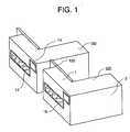
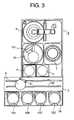
- each of vacuum processing apparatuses 100is composed of a rectangular block shaped cassette block 1 and a rectangular block shaped vacuum processing block 2.
- Each of the plan shapes of the cassette block 1 and the vacuum processing block 2is rectangular, and the whole plan shape formed by the both is L-shaped.
- the cassette block 1faces a bay path of a semiconductor manufacturing line and extends in the lateral direction of the bay path, and in the front side of the cassette block there are a cassette table 16 for receiving and sending a cassette 12 containing a sample from and to the bay path and an operation panel 14.
- the vacuum processing block 2 installed in the back side of the cassette block 1extends in the direction perpendicular to the cassette block 1 and contains various kinds of devices for performing vacuum processing and a transfer device.
- an atmospheric robot 9for transferring the sample and cassettes 12 for holding the sample.
- the sample cassettes 12are product sample cassettes 12A, 12B, 12C and a dummy sample cassette 12D.
- An orientation adjuster for the samplemay be provided near the cassettes 12, if necessary.
- the cassette 12contains only product samples or product and dummy samples. Samples for checking foreign substance and/or for cleaning are contained in the uppermost stage and/or the lowermost stage of the cassette.
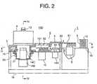
- a load side load lock chamber 4In the vacuum processing block 2, there are provided a load side load lock chamber 4, an unload side load lock chamber 5, a processing chamber 6, a post treating chamber 7, a vacuum pump 8 and a vacuum transfer robot 10.
- the reference character 13is a discharging means for etching
- the reference character 14is a discharging means for post treating (ashing).
- the atmospheric transfer robot 9is movably installed on a rail 92 placed parallel to the cassette table 16 inside the cassette block 1 to transfer a sample 3 the cassette 12 and the load lock chamber 4 in the load side and the load lock chamber 5 in the unload side.
- the vacuum transfer robot 10transfers the sample 3 from the load lock 5 in the load side to the processing chamber 6 and also transfers the sample 3 among the processing chamber 6, the load lock chamber 5 in the unload side and the post treating chamber 7.
- the present inventionis based on handling of a larger diameter sample having a diameter d above 12 inches (nearly 300 mm). When the diameter of the sample is 12 inches, the outer size C w of the cassette is nearly 350 mm to 360 mm.
- the processing chamber 6processes the sample 3 one-by-one, and is, for example, a chamber for performing plasma etching, and placed in the upper left of the vacuum processing block 2.
- the load lock chamber 4 in the load side and the load lock chamber 5 in the unload sideare placed in the opposite side of the processing chamber 6 across the vacuum transfer robot 10 each other, that is, the both are placed in the lower position of the vacuum processing block 2.
- the post treating chamber 7is a chamber for perform post treating to the processed sample 3 one-by-one, and placed in the middle position of the vacuum processing block 2 in facing the load lock chamber 5 in the unload side.
- the atmospheric transfer robot 9has an extensible arm 91 which is so designed that the locus of the extensible arm extending and contracting while the robot is moving on the rail 92 becomes the locus containing the cassette 12 in the loader and the load lock chamber 4 in the load side and the load lock chamber 5 in the unload side.
- the vacuum transfer robot 10has an extensible arm 101 which is so designed that the rotating locus of the extensible arm becomes the locus containing the load lock chamber 4 in the load side and the processing chamber 6, and is placed in the vacuum processing block 2. Therefore, the extensible arm 101 of the vacuum transfer robot is so installed that the rotating locus contains the processing chamber 6, the load lock chamber 5 in the unload side and the post treating chamber 7.
- the installed position of the atmospheric transfer robot 9may be in the right side position on the cassette block 1.
- a wafer search mechanismis provided around each of the cassettes 12 to recognize the samples in each of the cassettes when the cassette 12 is set.
- sample lifting mechanisms 14A, 14Brespectively, so that the sample 3 can be transferred to the extensible arm 91 or 101 in each of the robots.
- an electrode of an etching discharge means 13 and a sample mounting table 14CInside the etching discharge means 13, there is provided the sample lifting mechanism 14B.
- the reference character 15is a ring-shaped gate valve.
- the atmospheric transfer robot 9 in the cassette block 1is moved on the rail 92 to approach to, for example, the cassette 12A in the load side, and a fork (not shown) is inserted under the sample 3 inside the cassette in the load side by extending the extensible arm 91 toward the cassette 12A to mount the sample 3 on the fork.
- the arm 91 of the atmospheric transfer robot 9is moved to the load lock chamber 4 in the load side while the cover of the load lock chamber 4 in the load side is kept open to transfer the sample 3.
- the atmospheric transfer robot 9is moved on the rail 92 in such a manner that the stroke of the extensible arm 91 may reach the load lock chamber 4 in the load side, if necessary.
- the sample lifting mechanism 14Ais operated to support the sample 3 on a support member of the load lock chamber 4 in the load side. Further, after evacuating the load lock chamber 4 in the load side to a vacuum, the support member is lowered and the sample lifting mechanism 14A is operated again to transfer the sample to the arm 101 of the vacuum transfer robot 10 and transfer the sample along the transfer path inside the processing chamber 2, that is, to the processing chamber 6 in the vacuum environment. By the reverse operation, the sample is transferred to a cassette position in the unload side in the cassette block 1.
- the sampleis transferred to the post treating chamber 7 using the arm 101 of the vacuum transfer robot 10.
- the sample having been performed etching processingis performed plasma post treating such as ashing.
- the locus of the arm 101 of the vacuum transfer robot 10is as follows, in taking a case where the samples 3 are in the load lock chamber 4 in the load side, the processing chamber 6 and the post treating chamber 7 and no sample is in the load lock chamber 5 in the unload side. That is, the arm 101 of the vacuum transfer robot 10 is initially transfers the one sample 3 in the post treating chamber 7 to the load lock chamber 5 in the unload side, and the sample 3 in the proceessing chamber 6 is transferred to the post treating chamber 7. Next, the sample 3 in the load lock chamber 4 in the load side is transferred to the vacuum chamber 6. Further, the sample 3 in the treating chamber 6 is transferred to the post treating chamber 7. The arm 101 repeats to trace the same locus.
- the vacuum transfer robot 10Since the vacuum transfer robot 10 is placed near the side end of the vacuum processing block 2, a worker can inspect and repair the vacuum transfer robot with easy posture, and accordingly maintenance can be easily performed.
- FIG.5is a plan view showing an embodiment of a bay area 200 of a semiconductor manufacturing line having a vacuum processing apparatus 100 in accordance with the present invention.
- many L-shaped vacuum processing apparatuses 100are arranged in spacing a maintenance space 203 having a gap G1, and a partition 120 divides the room into a high clean level room 201A and a low clean level room 201B.
- An automatic transfer machine 202 for supplying and transferring samples 3is installed along the front surface of the cassette blocks 1 arranged in the high clean level room 201A.
- many vacuum processing blocks 2are arranged in the low clean level room 201B, and the interval between them is the maintenance space to be described later.
- FIG.6is a view showing a part of a flow of a sample 3 in an embodiment of a semiconductor manufacturing line in accordance with the present invention.
- an inspection apparatus 206At the entrance portion of each of the bay areas 200, there are provided an inspection apparatus 206 and a bay stoker 208.
- the back portion of each of the bay areas 200communicates to a maintenance path 210, and there is provided an air shower 212 in the entrance of the maintenance path 210.
- the sample 3 supplied to the bay stoker 208 from the externalis successively transferred to an in-bay automatic transfer machine 202 in a certain bay area 200 corresponding to the manufacturing process using a line automatic transfer machine 204, as shown by arrows.
- the sample 3is transferred from the in-bay automatic transfer machine 202 to the cassette block of the vacuum processing apparatus 100.
- the sample 3is transferred between the cassette block 1 and the vacuum processing block 2 by the atmospheric transfer robot 9 and the vacuum transfer robot 10.
- the sample 3 having processed in the vacuum processing block 2is transferred to the in-bay automatic transfer machine 202, and further transferred to the line automatic transfer machine 204, and then transferred to the next bay area 200.
- the in-bay automatic transfer machine 202supplies a new sample (unprocessed wafer) to the cassette block 1 in each of the vacuum processing apparatuses 100 from the bay stoker 208 provided in each of the bays 200, and recovers a cassette containing a processed sample from the cassette block 1.
- the in-bay automatic transfer machine 202receives a cassette containing a new sample (unprocessed wafer) from the bay stoker 208 provided in each of the bays 200, and runs up to and stops at a cassette position where the cassette block 1 of the vacuum processing apparatus outputs the requiring signal.
- a robothaving three-axis control function of rotating operation ( ⁇ -axis), vertical movement (Z-axis) and grip operation ( ⁇ -axis), or four-axis control function of rotating operation ( ⁇ -axis), vertical movement (Z-axis), grip operation ( ⁇ -axis) and back-and-forth movement (Y-axis) is used.
- the cassette handling robotrecovers the cassette 12 from the cassette block 1 to an empty cassette store on th in-bay automatic transfer machine 202, and then supplies a new cassette 12 transferred from the bay stoker 208 to the position made empty by recovering.
- the in-bay automatic transfer machinetransfers the recovered cassette 12 to the bay stoker 208, and stops its operation and stands by until the next requiring signal is output from the vacuum processing apparatus 100 in the bay 200.
- the in-bay automatic transfer machinetransfers samples according to order of time sequence of the received signals, or according to order of higher transfer efficiency from the stand-by position of the in-bay automatic transfer machine 202 in taking account of the relationship between the time difference in receiving signals and the positions of signal output apparatuses.
- Cassette managementis performed in such a manner that information on a received and sent cassette includes a number specified each of cassettes and various kinds of information used in managing the total manufacturing line, and is transmitted between the vacuum processing apparatus 100 and the in-bay automatic transfer machine 202 via, for example, an optical communication system.
- cassette block 1three to four cassettes 11, 12 are placed side by side on a plane in the same level.
- a given number of samplesin this case, semiconductor element substrates (wafers) having a diameter of 300 mm (12") are contained.
- the dummy waferis used for checking number of foreign particles in the vacuum processing portion and/or cleaning process of the processing chamber composing the vacuum processing zone.
- the cassettes 12 containing samples before processingbe called as 12A, 12B, 12C.
- a containing state of samples of, for example, the cassette 12Ais checked by a wafer check means (not shown).
- the cassette 12Ahas a function to store samples in vertical direction one-by-one.
- the wafer check means usedthere are a means where a sensor is successively moved so as to correspond to sample containing stages of the cassette 12A, and a means where plural sensors are provided corresponding to respective sample containing stages of the cassette 12A. In such a means, there is no need to provide a means for moving so as to correspond to sample containing stages of the cassette 12A. It may be possible to fix the sensor for wafer check means and move the cassette 12A instead.
- the wafer check meansUsing the wafer check means, it is checked in which positions in the vertical direction of the cassette 12A the unprocessed samples are contained.
- the wafer check meansis the type in which a sensor is successively moved so as to correspond to sample containing stages of the cassette 12A
- the sensordetects a sample containing stage of the cassette 12A and presence or absence of a unprocessed sample in the containing stage while the sensor is moving, for example, upward from the lower position of the cassette 12A, or downward from the upper position of the cassette 12A.
- the check resultsare output from the wafer check means to be input to and stored in, for example, a host computer (not shown in the figure) of the semiconductor manufacturing line control for managing the whole vacuum processing apparatuses. Otherwise, the check results may be input to and stored in a personal computer in a console box on the cassette mounting table or the host computer for controlling the apparatuses through the personal computer.
- the atmospheric transfer robot 9is started to operate.
- one of the unprocessed samples in the cassette 12Ais extracted out of the cassette 12A.
- the atmospheric transfer robot 9has a scooping-up device for scooping up and holding the surface of a sample opposite (reverse) to the surface to be processed.
- the scooping-up devices usedare a device adhering and holding the reverse side surface of the sample, a device having grooves or indented portions for holding the sample, and a device mechanically gripping the peripheral portion of the sample. Further, as the device adhering and holding the reverse side surface of the sample, there are devices having a function of vacuum sucking adhesion and a function of electrostatic attraction.
- interval between the adhering portionsis set to d/3 to d/2 taking the center of the sample as the center where d is the diameter of the sample.
- displacement of the sampleoccurs when the sample is transferred between the scooping-up device and another transfer means, which sometimes causes a trouble in displacement of the orientation of the sample.
- the adhering forceis required to have such a strength that the sample is not detached by the inertia force acting on the sample when the sample is being transferred including starting and stopping time. If this condition is not satisfied, a trouble occurs in falling of the sample from the scooping-up device or in displacement of the orientation of the sample.
- the scooping-up deviceis inserted in a position corresponding to the reverse surface of an unprocessed sample required to be extracted in the cassette 12A.
- the cassette 12AIn a state there the scooping-up device is inserted, the cassette 12A is lowered by a given amount or the scooping-up device is lifted by a given amount.
- the unprocessed sampleis transferred to the scooping-up device while the sample is kept in a scooped state.
- the scooping-up deviceextracts the sample out of the cassette 12A in keeping the state.
- one of the unprocessed samples in the cassette 12Ais extracted out of the cassette 12A.
- the host computerinstructs and controls the atmospheric transfer robot 9 which unprocessed sample in the cassette 12A is extracted.
- the information from which stage in the cassette 12A the unprocessed sample is extractedis successively stored in the host computer every extraction of the sample.
- the atmospheric transfer robot 9 having one unprocessed sample in the scooping-up deviceis moved to and stopped at a position where the sample can be loaded into the load lock chamber 4.
- the load lock chamber 4is isolated from a vacuum environment of the vacuum processing portion 2 and is in an atmospheric pressure state.
- the unprocessed sample held by the scooping-up device of the atmospheric transfer robot 9is loaded into the load lock chamber 4 in such a state to be transferred to the load lock chamber 4 from the scooping-up device.
- the atmospheric transfer robot 9 having transferred the unprocessed sample into the load lock chamber 4is returned to a predetermined position in standing by the next operation.
- the operation described aboveis instructed and controlled by, for example, the host computer.
- the information from which stage in the cassette 12A the unprocessed sample loaded in the load lock chamber 4 is extractedis successively stored in the host computer every extraction of the sample.
- the load lock chamber 4 having received the unprocessed sampleis isolated from atmosphere and evacuated to vacuum. Then, the isolation to the processing chamber is released and the load lock chamber 4 is communicated with the processing chamber to be capable of transferring the unprocessed sample. Then, a predetermined vacuum processing is performed in the vacuum processing zone.
- sample having been performed vacuum processing(sample after processed) is transferred from the vacuum processing zone to the unload lock chamber 5 by a vacuum transfer robot to be loaded into the unload lock chamber 5.
- the vacuum transfer robothas a scooping-up device similar to that in the atmospheric transfer robot 9.
- the scooping-up devicethe scooping devices similar to those of the atmospheric transfer robot 9 may be used except for the device having a function of vacuum adhesion.
- the unload lock chamber 5is isolated from the vacuum processing portion 2 and the pressure inside the unload lock chamber 5 is adjusted to atmospheric pressure.
- the unload lock chamber 5 in which the inner pressure becomes atmospheric pressureis opened to atmosphere. Under such a state, the scooping-up device of the atmospheric transfer robot 9 is inserted to the unload lock chamber 5, and the processed sample is transferred to the scooping-up device.
- the scooping-up devicehaving received the processed sample transfers the sample out of the unload lock chamber 5. After that, the unload lock chamber 5 is isolated from atmosphere and evacuated to a vacuum to be prepared for loading of the next processed sample.
- the atmospheric transfer robot 9 having the processed sample in the scooping-up deviceis moved to and stopped at a position where the processed sample can be returned into the cassette 12A.
- the scooping-up device having the processed sampleis inserted into the cassette 12A in keeping the state.
- the host computercontrols the inserting position so that the processed sample is returned to the position where the processed sample has been originally contained.
- the cassette 12AAfter inserting the scooping-up device having the processed sample, the cassette 12A is lifted or the scooping-up device is lowered.
- the processed sampleis returned to and contained in the position where the processed sample has been originally contained.
- Such operationis similarly performed to the remaining unprocessed samples in the cassette 12A and also to the unprocessed sample sin the cassettes 12B, 12C.
- the unprocessed sample successively extracted from each of the cassettes one by oneis, for example, numbered.
- the host computerfor example, stores information on that an unprocessed sample extracted from which stage in which cassette has what number.
- the host computerIn every movement of the sample from (1) to (8) as shown in the above, the host computer successively updates the information on what designated number sample each of the stations has. The updating processing is performed for every one of the samples. By doing so, each of the samples is managed, that is, it is managed what designated number sample exists in which station.
- the successive updating state process by the host computermay be successively displayed on a vacuum processing system control CRT screen.
- each of the stations and what designated number sample exists at presentare displayed so as to be easily recognized by an operator.
- this stepis performed between the above steps (2) and (3).
- Such management and control for movement of samplesmay be performed in a case where the vacuum processing portion 2 has a plurality of vacuum processing zones.
- the vacuum processing portion 2has, for example, two vacuum processing zones.
- the sampleis processed in series or processed in parallel depending on the processing information.
- the series processingmeans that a sample is vacuum-processed in one vacuum processing zone, and the processed sample is successively vacuum-processed in the remaining vacuum processing zone.
- the parallel processingmeans that a sample is vacuum-processed in one vacuum processing zone, and another sample is vacuum-processed in the remaining vacuum processing zone.
- a sample numbered by the host computeris processed according to a determined order and the processed sample is returned to the original position in the cassette.
- the host computermanages and controls in what vacuum processing zone and how a numbered sample is processed, the processed sample is returned to the original position in the cassette.
- the host computermay manage and control which vacuum processing zone is used depending on from which stage in the cassette the sample is extracted and what designated number the sample has.
- Examples of the plural vacuum processing zonesare a combination of zones having the same plasma generating method, a combination of different plasma etching zones, a combination of a plasma etching zone and a post-processing zone such as ashing, a combination of an etching zone and a film forming zone and so on.
- the dummy sample in a cassetteis handled in the same manner as for the unprocessed sample except for performing vacuum processing which is performed to the unprocessed sample.
- a detecting means for detecting presence or absence of a sampleis provided in each of the cassette, the scooping-up device of the atmospheric transfer robot, the orientation adjusting station, the station in the load lock chamber, the scooping-up device of the vacuum transfer robot, the station in the vacuum processing zone, the station in the unload lock chamber.
- a contact type or a non-contact type sensoris properly selected to be used as the sample detecting means.
- the cassette, the scooping-up device and each of the stationsbecome checking points for movement process of the sample.
- Such an embodimenthas the following usefulness.
- the processing statecan be identified by the information which stage in what cassette the defective sample is contained in. Therefore, the cause of the defect occurrence can be known in a short time and accordingly the time required for the countermeasure can be shortened by the time shortened in identification of the processing state.
- the above usefulnessis not limited to the diameter of the sample.
- FIG.7is a view showing the relationship between the size of the vacuum processing block 2 and the size of the cassette block 1.
- the side face of the vacuum processing block 2 of the vacuum processing apparatus 100 in accordance with the present inventionis of opening type door structure. That is, two pairs of hinged doors 214, 216 are provided in the side face and the back face of the vacuum processing block 2.
- the maintenance space MSis preferably 90 to 120 cm.
- an operatorcan easily access to the side face and the back face of the vacuum processing block 2. Further, by opening the doors 214, the load lock chamber 5, the post treating chamber 7, the vacuum transfer robot 10 and the various kinds of pipes and devices can be inspected and repaired. Furthermore, by opening the doors 216, the processing chamber 6 and the vacuum pump and the various kinds of pipes and devices can be inspected and repaired.
- the plan shape of the vacuum processing apparatus 100is L-shaped, as described before.
- the vacuum processing block and the cassette blockare generally constructed together to form a rectangular shape in the whole, as shown in FIG.9.
- the rectangular shapeis selected based on the shape of various kinds of elements installed in the vacuum processing apparatus and the mutual operational relationship among the various kinds of elements.
- G1the gap between the cassette blocks adjacent to each other
- G2the gap between the vacuum processing blocks adjacent to each other
- the conventional vacuum processing apparatus 800deals with samples having a diameter d not larger than 8 inches, such a construction described above can be used.
- the doors 214, 216must be made larger and a large maintenance space is required in order to keep a space for the doors 214, 216 to be opened.
- FIG. 10An embodiment of the mutual relationship of the various kinds of elements in the vacuum processing apparatus which can be used in the present invention will be described, referring to FIG. 10.
- the rotational center 01 of the arm of the vacuum transfer robot 10is arranged in the right hand side or the left hand side of the line L-L connecting the middle position of the load lock chamber 4 and the unload lock chamber 5 and the center of the processing chamber 6, that is, the rotational center 01 is shifted toward the side end side of the vacuum processing portion.
- the post treating chamber 7is arranged in the opposite side of the line L-L. Therefore, the rotating range of the arm of the vacuum transfer robot 10 is narrow, and the whole plan shape of the vacuum processing apparatus 100 can be made L-shaped by arranging the vacuum transfer robot 10 near the side end of the vacuum processing portion.
- the rotation range of the arm of the vacuum transfer robot 10becomes nearly one-half of one round circle.
- the rotating range of the arm of the vacuum robot 10 for transfer a waferto limit within nearly semi-circle, one sample 3 can be transferred to the load lock chamber 4, the unload lock chamber 5, the processing chamber 6 and the post treating chamber 7 within nearly semi-circle movement of the arm.
- the width W2 of the vacuum processing block 2can be made narrow.
- the vacuum processing apparatus 100keeps the aforementioned maintenance space by making the width W2 of the vacuum processing block 2 as small as possible in taking the shape of the various kinds of elements arranged in the vacuum processing apparatus and the mutual relationship of the various elements into consideration while the width W1 of the cassette block 1 copes with the large diameter sample. By doing so, the effective occupied area of the vacuum processing apparatus 100 can be increased.
- the positional relationship between the vacuum processing block 2 and the cassette block 1can be changed along the lateral direction of the cassette block.
- the vacuum processing block 2 and the cassette block 1are arranged so that the center line of the vacuum processing block 2 cross in the center of the cassette block 1 in the lateral direction, in other words, the vacuum processing block 2 and the cassette block 1 may be arranged so as to form a T-shape in the whole plan shape.
- the maintenance space MS between the vacuum processing blocks 2there is no obstacle in that the operator opens the doors 214 in the side to perform maintenance work.
- the structural elements contained in the cassette block 1 and the vacuum processing block 2 and the arrangement relationship the structural elementsmay be different from those in the aforementioned embodiments.
- the atmospheric transfer robot 9 of the cassette block 1is placed between the load lock chamber 4 and the unload lock chamber 5 of the vacuum processing block.
- the plan shape of the cassette block 1is strictly projecting shaped and the plan shape of the vacuum processing block 2 is strictly depressing shaped, and the whole of the vacuum processing apparatus 100 is a combination of two blocks of nearly rectangular shape forming a T-shape.
- the locus of the extensible arm 91can be constructed so as to trace the locus containing the cassette 12 and the load lock chamber 4 in the load side and the load lock chamber 5 in the unload side 5 without moving of the atmospheric transfer robot 9 on the rail by placing the atmospheric transfer robot 9 of the cassette block 1 between the load lock chamber 4 and the unload lock chamber 5 of the vacuum processing block and movably arranging the cassette 12 on the rail 94.
- the aforementioned maintenance space MS between the vacuum processing blocks 2can be kept.
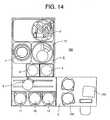
- FIG.14shows another embodiment of a vacuum processing apparatus 100.
- the vacuum processing apparatushas a cassette mounting table 130 and a console box 132 for evaluating and inspecting a sample in addition to a cassette block 1, an atmospheric transfer robot 9 and a sample cassette 12.
- FIG.15shows a further embodiment of a vacuum processing apparatus 100.
- the vacuum processing apparatusis a T-shaped vacuum processing apparatus having a cassette block 1, an atmospheric transfer robot 9 and a sample orientation adjuster 11.
- FIG.16is a plan view showing another embodiment of a bay area 200 in accordance with the present invention.
- a pair of L-shaped vacuum processing apparatuses 100A, 100Bare arranged opposite to each other to form a set, and a console box 132 is placed between the sets.
- There is not the aforementioned gap G1, but (W1+W3)-W2MS becomes the maintenance space when the width of the console box 132 is W3. Since there is no gap G1, an operator needs to enter the zone 201 placing the vacuum processing block 2 from the back of the bay area 200 through the maintenance path 210 in order to perform maintenance of the vacuum processing block 2.
- FIG.17is a plan view showing a bay area having another embodiment of a vacuum processing apparatuses in accordance with the present invention.
- the vacuum processing apparatus 100 in this embodimentcassette tables 16A for plural cassette blocks 1 are formed in a continuous one-piece structure, and a plurality of atmospheric transfer robots 9 run on a common rail 95 on the continuous cassette table.
- An in-bay automatic transfer machineis placed between the bar stoker and the atmospheric transfer robot 9 to transfer a sample between the vacuum processing blocks 2.
- the cassette block 1is functionally corresponds to each of the vacuum processing blocks 2 one by one, and it can be thought that a plurality of nearly rectangular blocks corresponding to the respective vacuum processing blocks 2 are connected together.
- FIG.18is a plan view showing the construction of an embodiment of a manufacturing line in accordance with the present invention. It can be understood from FIG.18 that the vacuum processing apparatus 100 in accordance with the present invention is L-shaped or T-shaped in plan shape and a sufficient maintenance space MS can be kept between the vacuum processing blocks 2 even if the gap between the vacuum processing apparatuses 100.
- the gap between the vacuum processing apparatusesmust be increased.
- number of vacuum processing apparatuses which can be arranged in the same length of lineis only five for the conventional rectangular vacuum processing apparatus 800 in comparing to seven for the vacuum processing apparatus 100 in accordance with the present invention as shown in the embodiment.
- the difference of two in number of vacuum processing apparatusesis large when the whole semiconductor manufacturing line is considered, and becomes a large difference in arranging a necessary number of apparatus in a clean room having a given space and in saving footprint.
- FIG.19is a plan view showing the whole construction of another embodiment of a semiconductor manufacturing line in which the vacuum processing apparatuses in accordance with the present invention are partially employed.
- This semiconductor manufacturing linehas a line automatic transfer machine 204 and is of a line automated type where transferring of a sample between each of the bay areas 200A to 200N and the line automatic transfer machine 204 is performed by an operator.
- the same effects as in the embodiment of FIG.18can be attained.
- FIG.20is a plan view showing the whole construction of a further embodiment of a semiconductor manufacturing line in which the vacuum processing apparatuses in accordance with the present invention are partially employed.
- This semiconductor manufacturing linehas in-bay automatic transfer machines 202 and a line automatic transfer machine 204 and is of a fully automated type where transferring of a sample inside each of the bat areas and between each of the bay areas 200A to 200N and the line automatic transfer machine 204 is performed without an operator.
- a proper maintenance space MScan be kept between the vacuum processing blocks.
- FIG.21 and FIG.22are further vacuum processing apparatuses which cannot be used in the present invention.
- the cassette 12is placed in a vacuum environment and the transfer robot 10 is operated in only a vacuum environment.
- FIG.21shows an example where two cassettes 12 are placed
- FIG.22shows an example where three cassettes 12 are placed. In the both cases, the whole vacuum processing apparatus is of a T-shape.
- a containing state of samples in the cassetteis performed by a wafer check means under a vacuum environment. Further, in an apparatus having an orientation adjusting means of an unprocessed sample, the orientation adjustment is performed under a vacuum environment.
- an apparatus having an intermediate cassette between the cassette and the vacuum processing zonethere are provided a robot for transferring the sample between the cassette and the intermediate cassette and a robot for transferring the sample between the intermediate cassette and the vacuum processing zone.
- the processed surface of a sampleis upside and the sample is held horizontal in a state when the sample is contained in the cassette, in a state when the sample is transferred and in a state when the sample is vacuum-processed.
- the other position of the sampleis no problem.
Landscapes
- Engineering & Computer Science (AREA)
- Physics & Mathematics (AREA)
- Condensed Matter Physics & Semiconductors (AREA)
- General Physics & Mathematics (AREA)
- Manufacturing & Machinery (AREA)
- Computer Hardware Design (AREA)
- Microelectronics & Electronic Packaging (AREA)
- Power Engineering (AREA)
- Container, Conveyance, Adherence, Positioning, Of Wafer (AREA)
- Physical Deposition Of Substances That Are Components Of Semiconductor Devices (AREA)
- Drying Of Semiconductors (AREA)
Description
- The present invention relates to a vacuum processing plant, and particularly relates to a vacuum processing apparatus suitable for performing treatment such as etching, chemical vapor deposit (CVD), spattering, ashing, rinsing or the like of a sample of semiconductor substrate such as Si substrate in a semiconductor manufacturing line for manufacturing semiconductor devices.
- Generally speaking, a vacuum processing apparatus is composed of a cassette block and a vacuum processing block. The cassette block has a front facing the bay path of the semiconductor manufacturing line and extending toward the longitudinal direction of the semiconductor manufacturing line, an alignment unit for aligning the orientation of a cassette for a sample or the orientation of a sample, and a robot operating under the atmospheric pressure environment. The vacuum block has a load lock chamber in the loading side, a load lock chamber in the unloading side, a processing chamber, a post treating chamber, a vacuum pump and a robot operating under a vacuum environment.
- In the vacuum processing apparatus, a sample extracted from the cassette in the cassette block is transferred to the load lock chamber of the vacuum processing block by the atmospheric transfer robot. The sample is further transferred to the processing chamber from the load lock chamber by the atmospheric transfer robot and set on an electrode structure body to be performed processing such as plasma treatment. Then the sample is transferred to the post treating chamber to be processed, if necessary. The sample having been processed is transferred to the cassette in the cassette block by the vacuum transfer robot and the atmospheric transfer robot.
- Vacuum processing apparatuses performing plasma etching to a sample are disclosed, for example, in Japanese Patent Publication No.61-8153, Japanese Patent Application Laid-Open No.63-133532, Japanese Patent Publication No.6-30369, Japanese Patent Application Laid-Open No.6-314729, Japanese Patent Application Laid-Open No.6-314730, and USP 5,314, 509.
- In the above conventional vacuum processing apparatus, the processing chambers and the load lock chambers are concentrically arranged or arranged in rectangular shape. For example, in the apparatus disclosed in USP 5,314,509, a vacuum transfer robot is arranged near the center of the vacuum processing block and three processing chambers are concentrically arranged around the vacuum transfer robot, a load lock chamber in the loading side and a load lock chamber in the unload side are provided between the vacuum transfer robot and the cassette block. In these apparatuses, there is a problem in that required installation area of the whole apparatus is large since the rotating angles of the transfer arms of the atmospheric transfer robot and the vacuum transfer robot are large.
- On the other hand, the processing chamber in the vacuum processing block and the vacuum pump and other various kind of piping components of the vacuum processing apparatus require maintenance such as scheduled and unscheduled inspection or repairing. Therefore, in general, there are provided doors around the vacuum processing block so that inspection and repairing of the load lock chamber, the un-load lock chamber, the processing chamber , the vacuum transfer robot and the various kind of piping components can be performed by opening the doors.
- In the conventional vacuum processing apparatus, there is a problem in that the installation area is large even though the sample to be handled has a diameter d smaller than 8 inches (1 inch = 2.54 cm) (nearly 200 mm) and the outer size of the cassette Cw is nearly 250 mm. Further, for a case of handling a large diameter sample having a diameter d above 12 inches (nearly 300 mm), the size of the cassette Cw becomes nearly 350 mm. Accordingly, the width of the cassette block containing a plurality of cassettes becomes large. If a width of the vacuum processing block is determined based on the width of the cassette block, the whole vacuum processing apparatus requires a large installation area. Considering a cassette block containing four cassettes as an example, the width of the cassette block cannot help increasing at least by nearly 40 cm when the diameter d of a sample increases from 8 inches to 12 inches.
- On the other hand, in a general semiconductor manufacturing line, in order to perform a large amount of samples and various kinds of processes, a plurality of vacuum processing apparatuses performing the same processing are gathered in a bay, and transmission between bays is performed automatically or manually. Since such a semiconductor manufacturing line requires a high cleanness, the whole semiconductor manufacturing line is installed in a large clean room. Increase in size of a vacuum processing apparatus due to increase in diameter of a sample to be processed results in increase in the installation area of the clean room, which further increases the construction cost of the clean room having a high construction cost in its nature. If vacuum processing apparatuses requiring a larger occupying installation area are installed in a clean room having the same area, it cannot help reducing total number of the vacuum processing apparatuses or decreasing in the spacing between the vacuum processing apparatuses. The reducing total number of the vacuum processing apparatuses in the clean room having the same area decreases the productivity of the semiconductor manufacturing line and increases the manufacturing cost of the semiconductor devices as an inevitable consequence. On the other hand, the decreasing in the spacing between the vacuum processing apparatuses decreases maintainability of the vacuum processing apparatus due to lack of maintenance space for inspection and repairing.
- An object of the present invention is to provide a vacuum processing plant capable of coping with larger diameter samples whilst keeping manufacturing cost to a minimum.
- Another object of the present invention is to provide a vacuum processing plant capable of coping with larger diameter samples at the same time having better maintainability.
- A further object of the present invention is to provide a semiconductor manufacturing line capable of coping with larger diameter samples whilst keeping manufacturing cost to a minimum by keeping the necessary number of vacuum processing apparatuses, through more economical use of space and at the same time not decreasing the maintainability.
- The present invention provides a vacuum processing plant as set out in
claim 1 and a method of operating the same as set out inclaim 3. - Therefore, in spite of a larger diameter sample, the number of vacuum processing apparatuses installed in a clean room,having the same area as a conventional clean room, does not need to be reduced. Accordingly productivity of the semiconductor manufacturing line does not decrease. Thus, it is possible to provide a vacuum processing apparatus which can cope with a larger diameter sample and, at the same time, can suppress increase in the manufacturing cost, and has better maintainability.
- Further, by employing the vacuum processing apparatus in a semiconductor manufacturing line according to the present invention, it is possible to provide the semiconductor manufacturing line which can cope with a larger diameter sample whilst keeping manufacturing cost to a minimum by keeping the necessary number of processing apparatuses, through more economical use of space and at the same time not decreasing the ease of maintainance.
- FIG.1 is a outer perspective view showing an embodiment of a vacuum processing apparatus which can be used in the present invention.
- FIG.2 is a vertical cross-sectional view showing the main portion of the apparatus of FIG.1.
- FIG.3 is a view showing the plan construction of the vacuum processing apparatus being taken on the plane of the line III-III of FIG.2.
- FIG.4 is a cross-sectional view showing the apparatus being taken on the plane of the line IV-IV of FIG.2.
- FIG.5 is a plan view showing an embodiment of a bay area of a semiconductor manufacturing line in accordance with the present invention.
- FIG.6 is a view showing a part of a sample flow in an embodiment of a semiconductor manufacturing line in accordance with the present invention.
- FIG.7 is a view showing the relationship between the size of a vacuum processing block and the size of a cassette block.
- FIG.8 is a view explaining maintenance of a vacuum block of a vacuum processing apparatus which can be used in the present invention.
- FIG.9 is a plan view showing the construction of an example of a conventional vacuum processing apparatus.
- FIG.10 is a view showing an example of the relative relationship of various kinds of elements inside a vacuum processing apparatus which can be used in the present invention.
- FIG.11 is a view showing a plan construction of another embodiment of a vacuum processing apparatus which can be used in the present invention.
- FIG.12 is a perspective view showing the vacuum processing apparatus of FIG.11.
- FIG.13 is a view showing a plan construction of another embodiment of a vacuum processing apparatus which can be used in the present invention.
- FIG. 14 is a view showing a plan construction of another embodiment of a vacuum processing apparatus which can be used in the present invention.
- FIG. 15 is a view showing a plan construction of another embodiment of a vacuum processing apparatus which can be used in the present invention.
- FIG.16 is a plan view showing anther embodiment of a bay area in accordance with the present invention.
- FIG. 17 is a plan view showing anther embodiment of a bay area in accordance with the present invention.
- FIG.18 is a plan view showing the construction of an embodiment of a semiconductor manufacturing line in accordance with the present invention.
- FIG.19 is a plan view showing the construction of an embodiment of a semiconductor manufacturing line in accordance with the present invention.
- FIG.20 is a plan view showing the construction of an embodiment of a semiconductor manufacturing line in accordance with the present invention.
- FIG.21 is a view showing the plan structure of a vacuum processing apparatus which cannot be used in the present invention.
- FIG.22 is a view showing the plan structure of a vacuum processing apparatus which cannot be used in the present invention.
- An embodiment of a vacuum processing apparatus which can be used in accordance with the present invention will be described in detail below, referring to FIG.1 to FIG.4. As shown in FIG.1, each of
vacuum processing apparatuses 100 is composed of a rectangular blockshaped cassette block 1 and a rectangular block shapedvacuum processing block 2. Each of the plan shapes of thecassette block 1 and thevacuum processing block 2 is rectangular, and the whole plan shape formed by the both is L-shaped. Thecassette block 1 faces a bay path of a semiconductor manufacturing line and extends in the lateral direction of the bay path, and in the front side of the cassette block there are a cassette table 16 for receiving and sending acassette 12 containing a sample from and to the bay path and anoperation panel 14. Thevacuum processing block 2 installed in the back side of thecassette block 1 extends in the direction perpendicular to thecassette block 1 and contains various kinds of devices for performing vacuum processing and a transfer device. - As shown in FIG.2 to FIG.4, in the
cassette block 1 there are provided anatmospheric robot 9 for transferring the sample andcassettes 12 for holding the sample. The sample cassettes 12 areproduct sample cassettes dummy sample cassette 12D. An orientation adjuster for the sample may be provided near thecassettes 12, if necessary. Thecassette 12 contains only product samples or product and dummy samples. Samples for checking foreign substance and/or for cleaning are contained in the uppermost stage and/or the lowermost stage of the cassette. - In the
vacuum processing block 2, there are provided a load sideload lock chamber 4, an unload sideload lock chamber 5, aprocessing chamber 6, apost treating chamber 7, avacuum pump 8 and avacuum transfer robot 10. Thereference character 13 is a discharging means for etching, and thereference character 14 is a discharging means for post treating (ashing). - The
atmospheric transfer robot 9 is movably installed on arail 92 placed parallel to the cassette table 16 inside thecassette block 1 to transfer asample 3 thecassette 12 and theload lock chamber 4 in the load side and theload lock chamber 5 in the unload side. Thevacuum transfer robot 10 transfers thesample 3 from theload lock 5 in the load side to theprocessing chamber 6 and also transfers thesample 3 among theprocessing chamber 6, theload lock chamber 5 in the unload side and thepost treating chamber 7. The present invention is based on handling of a larger diameter sample having a diameter d above 12 inches (nearly 300 mm). When the diameter of the sample is 12 inches, the outer size Cw of the cassette is nearly 350 mm to 360 mm. - The
processing chamber 6 processes thesample 3 one-by-one, and is, for example, a chamber for performing plasma etching, and placed in the upper left of thevacuum processing block 2. Theload lock chamber 4 in the load side and theload lock chamber 5 in the unload side are placed in the opposite side of theprocessing chamber 6 across thevacuum transfer robot 10 each other, that is, the both are placed in the lower position of thevacuum processing block 2. Thepost treating chamber 7 is a chamber for perform post treating to the processedsample 3 one-by-one, and placed in the middle position of thevacuum processing block 2 in facing theload lock chamber 5 in the unload side. - The
atmospheric transfer robot 9 has anextensible arm 91 which is so designed that the locus of the extensible arm extending and contracting while the robot is moving on therail 92 becomes the locus containing thecassette 12 in the loader and theload lock chamber 4 in the load side and theload lock chamber 5 in the unload side. Thevacuum transfer robot 10 has anextensible arm 101 which is so designed that the rotating locus of the extensible arm becomes the locus containing theload lock chamber 4 in the load side and theprocessing chamber 6, and is placed in thevacuum processing block 2. Therefore, theextensible arm 101 of the vacuum transfer robot is so installed that the rotating locus contains theprocessing chamber 6, theload lock chamber 5 in the unload side and thepost treating chamber 7. The installed position of theatmospheric transfer robot 9 may be in the right side position on thecassette block 1. - A wafer search mechanism is provided around each of the
cassettes 12 to recognize the samples in each of the cassettes when thecassette 12 is set. In theload lock chambers processing chamber 6 and thepost treating chamber 7, there are providedsample lifting mechanisms sample 3 can be transferred to theextensible arm processing chamber 6, there are provided an electrode of an etching discharge means 13 and a sample mounting table 14C. Inside the etching discharge means 13, there is provided thesample lifting mechanism 14B. Thereference character 15 is a ring-shaped gate valve. - Processing operation of a sample inside the
processing chamber 100 will be described below, in taking plasma etching process as an example. Initially, theatmospheric transfer robot 9 in thecassette block 1 is moved on therail 92 to approach to, for example, thecassette 12A in the load side, and a fork (not shown) is inserted under thesample 3 inside the cassette in the load side by extending theextensible arm 91 toward thecassette 12A to mount thesample 3 on the fork. After that, thearm 91 of theatmospheric transfer robot 9 is moved to theload lock chamber 4 in the load side while the cover of theload lock chamber 4 in the load side is kept open to transfer thesample 3. In this time, theatmospheric transfer robot 9 is moved on therail 92 in such a manner that the stroke of theextensible arm 91 may reach theload lock chamber 4 in the load side, if necessary. - Then, the
sample lifting mechanism 14A is operated to support thesample 3 on a support member of theload lock chamber 4 in the load side. Further, after evacuating theload lock chamber 4 in the load side to a vacuum, the support member is lowered and thesample lifting mechanism 14A is operated again to transfer the sample to thearm 101 of thevacuum transfer robot 10 and transfer the sample along the transfer path inside theprocessing chamber 2, that is, to theprocessing chamber 6 in the vacuum environment. By the reverse operation, the sample is transferred to a cassette position in the unload side in thecassette block 1. - In a case of requiring post treating, the sample is transferred to the
post treating chamber 7 using thearm 101 of thevacuum transfer robot 10. In thepost treating chamber 7, the sample having been performed etching processing is performed plasma post treating such as ashing. - In FIG.3, the locus of the
arm 101 of thevacuum transfer robot 10 is as follows, in taking a case where thesamples 3 are in theload lock chamber 4 in the load side, theprocessing chamber 6 and thepost treating chamber 7 and no sample is in theload lock chamber 5 in the unload side. That is, thearm 101 of thevacuum transfer robot 10 is initially transfers the onesample 3 in thepost treating chamber 7 to theload lock chamber 5 in the unload side, and thesample 3 in theproceessing chamber 6 is transferred to thepost treating chamber 7. Next, thesample 3 in theload lock chamber 4 in the load side is transferred to thevacuum chamber 6. Further, thesample 3 in the treatingchamber 6 is transferred to thepost treating chamber 7. Thearm 101 repeats to trace the same locus. - Since the
vacuum transfer robot 10 is placed near the side end of thevacuum processing block 2, a worker can inspect and repair the vacuum transfer robot with easy posture, and accordingly maintenance can be easily performed. - FIG.5 is a plan view showing an embodiment of a
bay area 200 of a semiconductor manufacturing line having avacuum processing apparatus 100 in accordance with the present invention. In the figure, many L-shapedvacuum processing apparatuses 100 are arranged in spacing amaintenance space 203 having a gap G1, and apartition 120 divides the room into a highclean level room 201A and a lowclean level room 201B. Anautomatic transfer machine 202 for supplying and transferringsamples 3 is installed along the front surface of the cassette blocks 1 arranged in the highclean level room 201A. On the other hand, many vacuum processing blocks 2 are arranged in the lowclean level room 201B, and the interval between them is the maintenance space to be described later. - FIG.6 is a view showing a part of a flow of a
sample 3 in an embodiment of a semiconductor manufacturing line in accordance with the present invention. At the entrance portion of each of thebay areas 200, there are provided aninspection apparatus 206 and abay stoker 208. The back portion of each of thebay areas 200 communicates to amaintenance path 210, and there is provided anair shower 212 in the entrance of themaintenance path 210. Thesample 3 supplied to thebay stoker 208 from the external is successively transferred to an in-bayautomatic transfer machine 202 in acertain bay area 200 corresponding to the manufacturing process using a lineautomatic transfer machine 204, as shown by arrows. Further, thesample 3 is transferred from the in-bayautomatic transfer machine 202 to the cassette block of thevacuum processing apparatus 100. In thevacuum processing apparatus 100, thesample 3 is transferred between thecassette block 1 and thevacuum processing block 2 by theatmospheric transfer robot 9 and thevacuum transfer robot 10. Thesample 3 having processed in thevacuum processing block 2 is transferred to the in-bayautomatic transfer machine 202, and further transferred to the lineautomatic transfer machine 204, and then transferred to thenext bay area 200. - In a semiconductor manufacturing line having an in-bay automatic transfer machine, the in-bay
automatic transfer machine 202 supplies a new sample (unprocessed wafer) to thecassette block 1 in each of thevacuum processing apparatuses 100 from thebay stoker 208 provided in each of thebays 200, and recovers a cassette containing a processed sample from thecassette block 1. - Corresponding to a requiring signal output from each of the
vacuum processing apparatuses 100, the in-bayautomatic transfer machine 202 receives a cassette containing a new sample (unprocessed wafer) from thebay stoker 208 provided in each of thebays 200, and runs up to and stops at a cassette position where thecassette block 1 of the vacuum processing apparatus outputs the requiring signal. - As a cassette handling robot installed in the in-bay
automatic transfer machine 202, a robot having three-axis control function of rotating operation (θ-axis), vertical movement (Z-axis) and grip operation (φ-axis), or four-axis control function of rotating operation (θ-axis), vertical movement (Z-axis), grip operation (φ-axis) and back-and-forth movement (Y-axis) is used. - In a case where a processed
cassette 12 has existed at a designated position in thecassette block 1, according to the required content output from each of thevacuum processing apparatuses 100 the cassette handling robot recovers thecassette 12 from thecassette block 1 to an empty cassette store on th in-bayautomatic transfer machine 202, and then supplies anew cassette 12 transferred from thebay stoker 208 to the position made empty by recovering. - After completion of this operation, the in-bay automatic transfer machine transfers the recovered
cassette 12 to thebay stoker 208, and stops its operation and stands by until the next requiring signal is output from thevacuum processing apparatus 100 in thebay 200. - When requiring signals are output from plural
vacuum processing apparatuses bay 200 within a short time, it depends on the system design whether the in-bay automatic transfer machine transfers samples according to order of time sequence of the received signals, or according to order of higher transfer efficiency from the stand-by position of the in-bayautomatic transfer machine 202 in taking account of the relationship between the time difference in receiving signals and the positions of signal output apparatuses. - Cassette management is performed in such a manner that information on a received and sent cassette includes a number specified each of cassettes and various kinds of information used in managing the total manufacturing line, and is transmitted between the
vacuum processing apparatus 100 and the in-bayautomatic transfer machine 202 via, for example, an optical communication system. - Processing flow in the
bay area 200 will be described below, in taking a sample in each cassette into consideration. - In the
cassette block 1, three to fourcassettes - In the two to three
cassettes 12 among the three to fourcassettes 12, samples to be performed certain vacuum processing in the vacuum processing portion (unprocessed wafers) are contained. In the remaining onecassette 11, dummy wafers are contained. - The dummy wafer is used for checking number of foreign particles in the vacuum processing portion and/or cleaning process of the processing chamber composing the vacuum processing zone.
- Here, letting the
cassettes 12 containing samples before processing be called as 12A, 12B, 12C. In such a state, a containing state of samples of, for example, thecassette 12A is checked by a wafer check means (not shown). In this case, thecassette 12A has a function to store samples in vertical direction one-by-one. - As the wafer check means used, there are a means where a sensor is successively moved so as to correspond to sample containing stages of the
cassette 12A, and a means where plural sensors are provided corresponding to respective sample containing stages of thecassette 12A. In such a means, there is no need to provide a means for moving so as to correspond to sample containing stages of thecassette 12A. It may be possible to fix the sensor for wafer check means and move thecassette 12A instead. - Using the wafer check means, it is checked in which positions in the vertical direction of the
cassette 12A the unprocessed samples are contained. For example, in a case where the wafer check means is the type in which a sensor is successively moved so as to correspond to sample containing stages of thecassette 12A, the sensor detects a sample containing stage of thecassette 12A and presence or absence of a unprocessed sample in the containing stage while the sensor is moving, for example, upward from the lower position of thecassette 12A, or downward from the upper position of thecassette 12A. - The check results are output from the wafer check means to be input to and stored in, for example, a host computer (not shown in the figure) of the semiconductor manufacturing line control for managing the whole vacuum processing apparatuses. Otherwise, the check results may be input to and stored in a personal computer in a console box on the cassette mounting table or the host computer for controlling the apparatuses through the personal computer.
- Then, in this embodiment, the
atmospheric transfer robot 9 is started to operate. By operation of theatmospheric transfer robot 9, one of the unprocessed samples in thecassette 12A is extracted out of thecassette 12A. - The
atmospheric transfer robot 9 has a scooping-up device for scooping up and holding the surface of a sample opposite (reverse) to the surface to be processed. The scooping-up devices used are a device adhering and holding the reverse side surface of the sample, a device having grooves or indented portions for holding the sample, and a device mechanically gripping the peripheral portion of the sample. Further, as the device adhering and holding the reverse side surface of the sample, there are devices having a function of vacuum sucking adhesion and a function of electrostatic attraction. - In a case of using the device adhering and holding the reverse side surface of the sample having a diameter of 300 mm (12"), it is important to select the arrangement and the dimension of the adhering portion so as to decrease bending of the sample as small as possible. For example, interval between the adhering portions is set to d/3 to d/2 taking the center of the sample as the center where d is the diameter of the sample.
- Depending on the amount of bending and the feature of bending of the sample, displacement of the sample occurs when the sample is transferred between the scooping-up device and another transfer means, which sometimes causes a trouble in displacement of the orientation of the sample.
- Further, in a case of using the device adhering and holding the reverse side surface of the sample, the adhering force is required to have such a strength that the sample is not detached by the inertia force acting on the sample when the sample is being transferred including starting and stopping time. If this condition is not satisfied, a trouble occurs in falling of the sample from the scooping-up device or in displacement of the orientation of the sample.
- The scooping-up device is inserted in a position corresponding to the reverse surface of an unprocessed sample required to be extracted in the
cassette 12A. In a state there the scooping-up device is inserted, thecassette 12A is lowered by a given amount or the scooping-up device is lifted by a given amount. By lowering of thecassette 12A or lifting of the scooping-up device, the unprocessed sample is transferred to the scooping-up device while the sample is kept in a scooped state. The scooping-up device extracts the sample out of thecassette 12A in keeping the state. Thus, one of the unprocessed samples in thecassette 12A is extracted out of thecassette 12A. - As described above, for example, the host computer instructs and controls the
atmospheric transfer robot 9 which unprocessed sample in thecassette 12A is extracted. - The information from which stage in the
cassette 12A the unprocessed sample is extracted is successively stored in the host computer every extraction of the sample. - The
atmospheric transfer robot 9 having one unprocessed sample in the scooping-up device is moved to and stopped at a position where the sample can be loaded into theload lock chamber 4. - The
load lock chamber 4 is isolated from a vacuum environment of thevacuum processing portion 2 and is in an atmospheric pressure state. The unprocessed sample held by the scooping-up device of theatmospheric transfer robot 9 is loaded into theload lock chamber 4 in such a state to be transferred to theload lock chamber 4 from the scooping-up device. - The
atmospheric transfer robot 9 having transferred the unprocessed sample into theload lock chamber 4 is returned to a predetermined position in standing by the next operation. - The operation described above is instructed and controlled by, for example, the host computer.
- The information from which stage in the
cassette 12A the unprocessed sample loaded in theload lock chamber 4 is extracted is successively stored in the host computer every extraction of the sample. - The
load lock chamber 4 having received the unprocessed sample is isolated from atmosphere and evacuated to vacuum. Then, the isolation to the processing chamber is released and theload lock chamber 4 is communicated with the processing chamber to be capable of transferring the unprocessed sample. Then, a predetermined vacuum processing is performed in the vacuum processing zone. - The sample having been performed vacuum processing (sample after processed) is transferred from the vacuum processing zone to the unload
lock chamber 5 by a vacuum transfer robot to be loaded into the unloadlock chamber 5. - The vacuum transfer robot has a scooping-up device similar to that in the
atmospheric transfer robot 9. As the scooping-up device, the scooping devices similar to those of theatmospheric transfer robot 9 may be used except for the device having a function of vacuum adhesion. - After loading the processed sample, the unload
lock chamber 5 is isolated from thevacuum processing portion 2 and the pressure inside the unloadlock chamber 5 is adjusted to atmospheric pressure. - The unload
lock chamber 5 in which the inner pressure becomes atmospheric pressure is opened to atmosphere. Under such a state, the scooping-up device of theatmospheric transfer robot 9 is inserted to the unloadlock chamber 5, and the processed sample is transferred to the scooping-up device. - The scooping-up device having received the processed sample transfers the sample out of the unload
lock chamber 5. After that, the unloadlock chamber 5 is isolated from atmosphere and evacuated to a vacuum to be prepared for loading of the next processed sample. - On the other hand, the
atmospheric transfer robot 9 having the processed sample in the scooping-up device is moved to and stopped at a position where the processed sample can be returned into thecassette 12A. - Then, the scooping-up device having the processed sample is inserted into the
cassette 12A in keeping the state. The host computer controls the inserting position so that the processed sample is returned to the position where the processed sample has been originally contained. - After inserting the scooping-up device having the processed sample, the
cassette 12A is lifted or the scooping-up device is lowered. - By doing so, the processed sample is returned to and contained in the position where the processed sample has been originally contained.
- Such operation is similarly performed to the remaining unprocessed samples in the
cassette 12A and also to the unprocessed sample sin thecassettes - That is, the unprocessed sample successively extracted from each of the cassettes one by one is, for example, numbered. The host computer, for example, stores information on that an unprocessed sample extracted from which stage in which cassette has what number.
- Based on the information, movement of a sample, extraction of the sample from a cassette, performing of vacuum processing to the sample and returning of the sample to the cassette after vacuum processing, is managed and controlled.
- In other words, the movement of a sample from being extracted to being returned to the original cassette, is performed according to the steps in the following order.
- (1) checking of a containing position in a cassette.
- (2) extraction of a sample in the cassette using an atmospheric transfer robot.
- (3) loading of the sample into a load lock chamber using an atmospheric transfer robot.
- (4) transferring of the sample from load lock chamber to a vacuum processing zone using a vacuum transfer robot.
- (5) performing vacuum processing in the vacuum processing zone.
- (6) transferring of the sample from the vacuum processing zone to an unload lock chamber using the vacuum transfer robot.
- (7) unloading of the sample from the unload lock chamber using the atmospheric transfer robot.
- (8) containing of the sample into the original position in the cassette using the atmospheric transfer robot.
- In every movement of the sample from (1) to (8) as shown in the above, the host computer successively updates the information on what designated number sample each of the stations has. The updating processing is performed for every one of the samples. By doing so, each of the samples is managed, that is, it is managed what designated number sample exists in which station.
- For example, the successive updating state process by the host computer may be successively displayed on a vacuum processing system control CRT screen. In this case, each of the stations and what designated number sample exists at present are displayed so as to be easily recognized by an operator.
- In a case where orientation adjustment of an unprocessed sample is performed, this step is performed between the above steps (2) and (3).
- Such management and control for movement of samples may be performed in a case where the
vacuum processing portion 2 has a plurality of vacuum processing zones. - Assuming that the
vacuum processing portion 2 has, for example, two vacuum processing zones. In this case, the sample is processed in series or processed in parallel depending on the processing information. Here, the series processing means that a sample is vacuum-processed in one vacuum processing zone, and the processed sample is successively vacuum-processed in the remaining vacuum processing zone. The parallel processing means that a sample is vacuum-processed in one vacuum processing zone, and another sample is vacuum-processed in the remaining vacuum processing zone. - In a case of series processing, a sample numbered by the host computer is processed according to a determined order and the processed sample is returned to the original position in the cassette.
- In a case of parallel processing, since the host computer manages and controls in what vacuum processing zone and how a numbered sample is processed, the processed sample is returned to the original position in the cassette.
- In a case of parallel processing, the host computer may manage and control which vacuum processing zone is used depending on from which stage in the cassette the sample is extracted and what designated number the sample has.
- In a case where series processing and parallel processing are mixed, since the host computer manages and controls in what vacuum processing zone and how a numbered sample is processed, the processed sample is returned to the original position in the cassette.
- Examples of the plural vacuum processing zones are a combination of zones having the same plasma generating method, a combination of different plasma etching zones, a combination of a plasma etching zone and a post-processing zone such as ashing, a combination of an etching zone and a film forming zone and so on.
- The dummy sample in a cassette is handled in the same manner as for the unprocessed sample except for performing vacuum processing which is performed to the unprocessed sample.
- A detecting means for detecting presence or absence of a sample is provided in each of the cassette, the scooping-up device of the atmospheric transfer robot, the orientation adjusting station, the station in the load lock chamber, the scooping-up device of the vacuum transfer robot, the station in the vacuum processing zone, the station in the unload lock chamber.
- A contact type or a non-contact type sensor is properly selected to be used as the sample detecting means.
- The cassette, the scooping-up device and each of the stations become checking points for movement process of the sample.
- In such a construction, for example, when presence of a sample is detected in the scooping-up device of the
vacuum transfer robot 10 and presence of a sample is not detected in the station in the vacuum processing zone, this means that a trouble occurs in the sample transfer machine between the scooping-up device of the vacuum transfer robot and the station in the vacuum processing zone due to some cause, and recovering for the trouble can be properly and speedy preformed. Therefore, it is possible to prevent the through-put of the whole system from decreasing. - In a construction where the sample detecting means is not provided in each of the scooping-up devices of the
transfer robots 9, for example, when presence of a sample is detected in the station in the load lock chamber and presence of a sample is not detected in the station in the vacuum processing zone, this means that a trouble occurs in the sample transfer machine between the station in the load lock chamber and the scooping-up device of the vacuum transfer robot, or in the vacuum transfer robot, or the sample transfer machine between the scooping-up device of the vacuum transfer robot and the station in the vacuum processing zone due to some cause, and recovering for the trouble can be properly and speedy preformed. Therefore, it is possible to prevent the through-put of the whole system from decreasing. - Such an embodiment has the following usefulness.
- (1) Since which stage in the cassette an unprocessed sample is contained is checked and movement of the checked unprocessed sample is successively managed and controlled by numbering the unprocessed sample, the processed sample can be certainly returned to the original position of the cassette.
- (2) Since which stage in the cassette an unprocessed sample is contained is checked and movement of the checked unprocessed sample is successively managed and controlled by numbering the unprocessed sample even in a case of series processing, parallel processing or mixed processing of the both, the processed sample can be certainly returned to the original position of the cassette.
- (3) Since which stage in the cassette an unprocessed sample is contained is checked and movement of the checked unprocessed sample is successively managed and controlled by numbering the unprocessed sample, the processing state of the sample processed in the vacuum processing portion one by one can be properly checked and managed in detail.
- For example, in a case where a defect occurs in the process of the sample, since a processing state for each of the samples including processing condition is managed, the processing state can be identified by the information which stage in what cassette the defective sample is contained in. Therefore, the cause of the defect occurrence can be known in a short time and accordingly the time required for the countermeasure can be shortened by the time shortened in identification of the processing state.
- Although the description in the above embodiment is based on that the diameter of the sample is 300 mm (12"), the above usefulness is not limited to the diameter of the sample.
- The maintenance will be described below.
- As for maintenance of the
vacuum processing apparatus 100 most of the maintenance of thecassette block 1 can be performed from the front side of the cassette block since thecassette block 1 faces the line of in-bayautomatic transfer machine 202. - On the other hand, as for the maintenance of the
vacuum processing block 2, an operator is required to enter the area placing thevacuum processing block 2 from the back side of each bay area through themaintenance path 203 or through themaintenance path 210. - FIG.7 is a view showing the relationship between the size of the
vacuum processing block 2 and the size of thecassette block 1. When the longer side (width) of thevacuum processing block 2 is written by W1 and the shorter side is written by B1, and the longer side (width) of thecassette block 1 is written by W2 and the shorter side is written by B2, the relations W1>B1, W2>B2 are satisfied. It is preferable that the relation W1-W2=d is satisfied where d is the diameter of the sample. - When the gap between the cassette blocks of the vacuum processing apparatuses adjacent to each other is written by G1 and the gap between the vacuum processing blocks adjacent to each other is written by G2 (referring to FIG.5), it is assumed that the relation G1<G2 is satisfied. Maintenance space between the
vacuum processing apparatuses 100 adjacent to each other can be expressed by (W1+G1)-W2=MS. MS is a dimension required for maintenance work of an operator. In this case, it is preferable that the relation (W1+G1)-W2=d is satisfied. Although themaintenance space 203 is an entrance for the operator, there are some cases where the space is not provided depending on the layout of thebay area 200. Even in such a case, an installation clearance G1 between the vacuum processing apparatuses adjacent to each other is required at minimum, but the installation clearance practically becomes a value near zero. In this case, W1-W2=MS becomes the maintenance space. - The side face of the
vacuum processing block 2 of thevacuum processing apparatus 100 in accordance with the present invention is of opening type door structure. That is, two pairs of hingeddoors vacuum processing block 2. - In order to perform maintenance, it is required that (1) there are spaces from which an operator can check the devices and the pipes from back and front sides, (2) there are spaces to which the various kinds of devices and pipes, for example, the main chamber can be drawn, and (3) there are spaces in which the doors can be opened. Therefore, the maintenance space MS is preferably 90 to 120 cm.
- According to the
vacuum processing apparatus 100, an operator can easily access to the side face and the back face of thevacuum processing block 2. Further, by opening thedoors 214, theload lock chamber 5, thepost treating chamber 7, thevacuum transfer robot 10 and the various kinds of pipes and devices can be inspected and repaired. Furthermore, by opening thedoors 216, theprocessing chamber 6 and the vacuum pump and the various kinds of pipes and devices can be inspected and repaired. - Since there is the maintenance space MS between the vacuum processing blocks 2, there is no obstacle in that the operator opens the
doors 214 in the side to perform maintenance work. Further, there is provided an enough space in the back face side of thevacuum processing block 2 to open thedoors 216 and perform maintenance work. - The plan shape of the
vacuum processing apparatus 100 is L-shaped, as described before. On the other hand, in the conventionalvacuum processing apparatus 800, the vacuum processing block and the cassette block are generally constructed together to form a rectangular shape in the whole, as shown in FIG.9. The rectangular shape is selected based on the shape of various kinds of elements installed in the vacuum processing apparatus and the mutual operational relationship among the various kinds of elements. In the general conventional vacuum processing apparatus, when the gap between the cassette blocks adjacent to each other is written by G1 and the gap between the vacuum processing blocks adjacent to each other is written by G2, there is the relation G1≥G2. - Since the conventional
vacuum processing apparatus 800 deals with samples having a diameter d not larger than 8 inches, such a construction described above can be used. However, in an apparatus dealing with a sample having a diameter d as large as 12 inches, the outer dimension of thecassette 12 becomes larger and consequently the width W1 of the cassette block containing a plurality of thecassette 12 becomes larger.Since the width (W2=W1) of the vacuum processing block is determined corresponding to the width W1, the whole of thevacuum processing apparatus 800 requires a larger space. Further, as the widths W1, W2 of the cassette block and the vacuum processing block become larger, thedoors doors vacuum processing apparatuses 100 adjacent to each other becomes MS=90 cm. This results in increase in effective occupying area of thevacuum processing apparatus 800 in each of the bay areas. This is not preferable. - An embodiment of the mutual relationship of the various kinds of elements in the vacuum processing apparatus which can be used in the present invention will be described, referring to FIG. 10. As shown in the figure, the
rotational center 01 of the arm of thevacuum transfer robot 10 is arranged in the right hand side or the left hand side of the line L-L connecting the middle position of theload lock chamber 4 and the unloadlock chamber 5 and the center of theprocessing chamber 6, that is, therotational center 01 is shifted toward the side end side of the vacuum processing portion. Thepost treating chamber 7 is arranged in the opposite side of the line L-L. Therefore, the rotating range of the arm of thevacuum transfer robot 10 is narrow, and the whole plan shape of thevacuum processing apparatus 100 can be made L-shaped by arranging thevacuum transfer robot 10 near the side end of the vacuum processing portion. By such a construction,the rotation range of the arm of thevacuum transfer robot 10 becomes nearly one-half of one round circle. By making the rotating range of the arm of thevacuum robot 10 for transfer a wafer to limit within nearly semi-circle, onesample 3 can be transferred to theload lock chamber 4, the unloadlock chamber 5, theprocessing chamber 6 and thepost treating chamber 7 within nearly semi-circle movement of the arm. As described above, since the rotating range of the arm of thevacuum transfer robot 10 is designed within nearly semi-circle, the width W2 of thevacuum processing block 2 can be made narrow. - As described above, the
vacuum processing apparatus 100 keeps the aforementioned maintenance space by making the width W2 of thevacuum processing block 2 as small as possible in taking the shape of the various kinds of elements arranged in the vacuum processing apparatus and the mutual relationship of the various elements into consideration while the width W1 of thecassette block 1 copes with the large diameter sample. By doing so, the effective occupied area of thevacuum processing apparatus 100 can be increased. - Since there is the maintenance space MS between the vacuum processing blocks 2, there is no obstacle in that the operator opens the
doors 214 in the side to perform maintenance work. Further, there is provided an enough space in the back face side of thevacuum processing block 2 to open thedoors 216 and perform maintenance work. - In the
vacuum processing apparatus 100, the positional relationship between thevacuum processing block 2 and thecassette block 1 can be changed along the lateral direction of the cassette block. For example, as shown in FIG.11 and FIG.12, thevacuum processing block 2 and thecassette block 1 are arranged so that the center line of thevacuum processing block 2 cross in the center of thecassette block 1 in the lateral direction, in other words, thevacuum processing block 2 and thecassette block 1 may be arranged so as to form a T-shape in the whole plan shape. In the T-shape arrangement, since there is the maintenance space MS between the vacuum processing blocks 2, there is no obstacle in that the operator opens thedoors 214 in the side to perform maintenance work. - The plan shape of the
cassette block 1 and thevacuum processing block 2 in accordance with the present invention may be not strictly rectangular, that is, nearly rectangular as far as the relation (W1+G1)-W2=MS is practically kept. The structural elements contained in thecassette block 1 and thevacuum processing block 2 and the arrangement relationship the structural elements may be different from those in the aforementioned embodiments. For example, in the embodiment shown in FIG.13, theatmospheric transfer robot 9 of thecassette block 1 is placed between theload lock chamber 4 and the unloadlock chamber 5 of the vacuum processing block. In this case, the plan shape of thecassette block 1 is strictly projecting shaped and the plan shape of thevacuum processing block 2 is strictly depressing shaped, and the whole of thevacuum processing apparatus 100 is a combination of two blocks of nearly rectangular shape forming a T-shape. In this embodiment, the locus of theextensible arm 91 can be constructed so as to trace the locus containing thecassette 12 and theload lock chamber 4 in the load side and theload lock chamber 5 in the unloadside 5 without moving of theatmospheric transfer robot 9 on the rail by placing theatmospheric transfer robot 9 of thecassette block 1 between theload lock chamber 4 and the unloadlock chamber 5 of the vacuum processing block and movably arranging thecassette 12 on therail 94. In this embodiment, the aforementioned maintenance space MS between the vacuum processing blocks 2 can be kept. - FIG.14 shows another embodiment of a
vacuum processing apparatus 100. The vacuum processing apparatus has a cassette mounting table 130 and aconsole box 132 for evaluating and inspecting a sample in addition to acassette block 1, anatmospheric transfer robot 9 and asample cassette 12. - FIG.15 shows a further embodiment of a
vacuum processing apparatus 100. The vacuum processing apparatus is a T-shaped vacuum processing apparatus having acassette block 1, anatmospheric transfer robot 9 and asample orientation adjuster 11. - FIG.16 is a plan view showing another embodiment of a
bay area 200 in accordance with the present invention. A pair of L-shapedvacuum processing apparatuses console box 132 is placed between the sets. There is not the aforementioned gap G1, but (W1+W3)-W2=MS becomes the maintenance space when the width of theconsole box 132 is W3. Since there is no gap G1, an operator needs to enter the zone 201 placing thevacuum processing block 2 from the back of thebay area 200 through themaintenance path 210 in order to perform maintenance of thevacuum processing block 2. If it is required to reduce the access time, a gap G1 may be provided between theconsole box 132 and the neighboringcassette block 1. In this case, (W1+W3+G1)-W2=MS becomes the maintenance space. - FIG.17 is a plan view showing a bay area having another embodiment of a vacuum processing apparatuses in accordance with the present invention. The
vacuum processing apparatus 100 in this embodiment, cassette tables 16A for plural cassette blocks 1 are formed in a continuous one-piece structure, and a plurality ofatmospheric transfer robots 9 run on acommon rail 95 on the continuous cassette table. An in-bay automatic transfer machine is placed between the bar stoker and theatmospheric transfer robot 9 to transfer a sample between the vacuum processing blocks 2. In this case, thecassette block 1 is functionally corresponds to each of the vacuum processing blocks 2 one by one, and it can be thought that a plurality of nearly rectangular blocks corresponding to the respective vacuum processing blocks 2 are connected together. - FIG.18 is a plan view showing the construction of an embodiment of a manufacturing line in accordance with the present invention. It can be understood from FIG.18 that the
vacuum processing apparatus 100 in accordance with the present invention is L-shaped or T-shaped in plan shape and a sufficient maintenance space MS can be kept between the vacuum processing blocks 2 even if the gap between thevacuum processing apparatuses 100. - On the other hand, if the sufficient maintenance space is provided in the conventional rectangular
vacuum processing apparatus 800 shown for the purpose of comparison, the gap between the vacuum processing apparatuses must be increased. As the result, number of vacuum processing apparatuses which can be arranged in the same length of line is only five for the conventional rectangularvacuum processing apparatus 800 in comparing to seven for thevacuum processing apparatus 100 in accordance with the present invention as shown in the embodiment. The difference of two in number of vacuum processing apparatuses is large when the whole semiconductor manufacturing line is considered, and becomes a large difference in arranging a necessary number of apparatus in a clean room having a given space and in saving footprint. As for transferring of sample from a bay area having an automatic transfer machine to a bay area for the next process, when the vacuum processing apparatus in accordance with the present invention is employed, an amount of processing corresponding to seven vacuum processing apparatuses can be performed using one side of the one bay area. Whereas, when the conventional apparatus is employed, an amount of processing corresponding to only five vacuum processing apparatuses can be performed. This difference of two apparatuses largely affects on improvement of through-put in a semiconductor manufacturing line. - There are some cases where the rectangular
vacuum processing apparatus 800 is required to be partially used. Even in such a case, by arranging the L-shaped or T-shapedvacuum processing apparatus 100 in accordance with the present invention adjacent to the rectangularvacuum processing apparatus 800, a proper maintenance space MS can be kept between the vacuum processing blocks. - FIG.19 is a plan view showing the whole construction of another embodiment of a semiconductor manufacturing line in which the vacuum processing apparatuses in accordance with the present invention are partially employed. This semiconductor manufacturing line has a line
automatic transfer machine 204 and is of a line automated type where transferring of a sample between each of thebay areas 200A to 200N and the lineautomatic transfer machine 204 is performed by an operator. In this system, the same effects as in the embodiment of FIG.18 can be attained. - FIG.20 is a plan view showing the whole construction of a further embodiment of a semiconductor manufacturing line in which the vacuum processing apparatuses in accordance with the present invention are partially employed. This semiconductor manufacturing line has in-bay
automatic transfer machines 202 and a lineautomatic transfer machine 204 and is of a fully automated type where transferring of a sample inside each of the bat areas and between each of thebay areas 200A to 200N and the lineautomatic transfer machine 204 is performed without an operator. In this case, by arranging the L-shaped or T-shapedvacuum processing apparatuses 100 adjacent to each other or by arranging the L-shaped or T-shapedvacuum processing apparatus 100 in accordance with the present invention adjacent to the rectangularvacuum processing apparatus 800, a proper maintenance space MS can be kept between the vacuum processing blocks. - In the aforementioned embodiments, it has been described that the cassette and the atmospheric transfer robot are placed in an atmospheric environment and the atmospheric transfer robot is operated in an atmospheric environment. Shown in FIG.21 and FIG.22 are further vacuum processing apparatuses which cannot be used in the present invention. Here it is possible that the
cassette 12 is placed in a vacuum environment and thetransfer robot 10 is operated in only a vacuum environment. FIG.21 shows an example where twocassettes 12 are placed, and FIG.22 shows an example where threecassettes 12 are placed. In the both cases, the whole vacuum processing apparatus is of a T-shape. - In FIG.21 and FIG.22, extraction of a sample in the
cassette 12, transferring of the extracted sample to the vacuum processing zone, transferring of the sample from the vacuum processing zone and storing of the sample to the original position in the cassette are performed under a vacuum environment using thevacuum transfer robot 10. In these cases, in regard to the vacuum processing system, there is no need to provide the load lock chamber and the unload lock chamber in the aforementioned embodiments, in principle. Therefore, number of data elements successively updated by the host computer is reduced by number of the data elements used for the load lock chamber and the unload lock chamber. - In this case, a containing state of samples in the cassette is performed by a wafer check means under a vacuum environment. Further, in an apparatus having an orientation adjusting means of an unprocessed sample, the orientation adjustment is performed under a vacuum environment.
- Furthermore, in an apparatus having an intermediate cassette between the cassette and the vacuum processing zone, there are provided a robot for transferring the sample between the cassette and the intermediate cassette and a robot for transferring the sample between the intermediate cassette and the vacuum processing zone.
- In such a vacuum processing system, since the intermediate cassette is added, number of data elements successively updated by the host computer is increased by number of the data elements used for the intermediate cassette and the robot.
- Still further, in the aforementioned embodiments, the processed surface of a sample is upside and the sample is held horizontal in a state when the sample is contained in the cassette, in a state when the sample is transferred and in a state when the sample is vacuum-processed. However, the other position of the sample is no problem.
- As having been described above, according to the present invention, it is possible to provide a vacuum processing apparatus capable of coping with larger diameter samples and capable of suppressing increase in manufacturing cost, and at the same time having a better maintainability.
- Further, it is possible to provide a semiconductor manufacturing line capable of coping with larger diameter samples and at the same time capable of suppressing increase in manufacturing cost by maintaining necessary installation number of vacuum processing apparatuses and not decreasing the maintainability by employing the aforementioned vacuum processing apparatuses in the semiconductor manufacturing line in accordance with the present invention.
Claims (3)
- A vacuum processing plant for processing in a vacuum substrates in semiconductor manufacture, having
a plurality of independent vacuum processing blocks (2) arranged in a row, each vacuum processing block (2) containing vacuum processing means for processing in a vacuum the substrates and a transfer device (10) for transferring the substrates within said vacuum processing block (2),
a plurality of cassette blocks (1) arranged along said row in front of said vacuum processing blocks (2), each cassette block (1) having a cassette table (16) for holding substrate-carrying cassettes (12) under atmospheric pressure and transfer means (9) for transferring under atmospheric pressure substrates between cassettes (12) on the cassette table (16) and the adjacent vacuum processing block (2),
wherein each said vacuum processing block (2) is narrower, in the direction along said row than the adjacent cassette block (1), whereby together they have a T or L shape in plan view,
the plant having a first space (201B) extending behind and between said vacuum processing blocks for maintenance thereof and a second space (201A), in which said cassette blocks are located, the first and second spaces (201A, 201B) being closed off from each other. - A vacuum processing plant according to claim 1, wherein an automatic transfer machine (202) runs in said second space (201A) to convey cassettes to and from said cassette blocks (2).
- A method of operating a vacuum processing plant according to claim 1 or 2, wherein a higher cleanness level is maintained in said second space (201A) than in said first space (201B).
Applications Claiming Priority (3)
| Application Number | Priority Date | Filing Date | Title |
|---|---|---|---|
| JP18292195 | 1995-07-19 | ||
| JP7182921AJPH0936198A (en) | 1995-07-19 | 1995-07-19 | Vacuum processing apparatus and semiconductor manufacturing line using the same |
| EP96305154AEP0756316B1 (en) | 1995-07-19 | 1996-07-12 | Vacuum processing apparatus and semiconductor manufacturing line using the same |
Related Parent Applications (1)
| Application Number | Title | Priority Date | Filing Date |
|---|---|---|---|
| EP96305154ADivisionEP0756316B1 (en) | 1995-07-19 | 1996-07-12 | Vacuum processing apparatus and semiconductor manufacturing line using the same |
Publications (3)
| Publication Number | Publication Date |
|---|---|
| EP1119022A2 EP1119022A2 (en) | 2001-07-25 |
| EP1119022A3 EP1119022A3 (en) | 2003-10-15 |
| EP1119022B1true EP1119022B1 (en) | 2007-01-24 |
Family
ID=16126714
Family Applications (3)
| Application Number | Title | Priority Date | Filing Date |
|---|---|---|---|
| EP01104776AExpired - LifetimeEP1143488B1 (en) | 1995-07-19 | 1996-07-12 | Vacuum processing apparatus and semiconductor manufacturing line using the same |
| EP01104775AExpired - LifetimeEP1119022B1 (en) | 1995-07-19 | 1996-07-12 | Vacuum processing apparatus and semiconductor manufacturing line using the same |
| EP96305154AExpired - LifetimeEP0756316B1 (en) | 1995-07-19 | 1996-07-12 | Vacuum processing apparatus and semiconductor manufacturing line using the same |
Family Applications Before (1)
| Application Number | Title | Priority Date | Filing Date |
|---|---|---|---|
| EP01104776AExpired - LifetimeEP1143488B1 (en) | 1995-07-19 | 1996-07-12 | Vacuum processing apparatus and semiconductor manufacturing line using the same |
Family Applications After (1)
| Application Number | Title | Priority Date | Filing Date |
|---|---|---|---|
| EP96305154AExpired - LifetimeEP0756316B1 (en) | 1995-07-19 | 1996-07-12 | Vacuum processing apparatus and semiconductor manufacturing line using the same |
Country Status (7)
| Country | Link |
|---|---|
| US (18) | US5855726A (en) |
| EP (3) | EP1143488B1 (en) |
| JP (1) | JPH0936198A (en) |
| KR (2) | KR100440683B1 (en) |
| DE (3) | DE69636872T2 (en) |
| SG (1) | SG52824A1 (en) |
| TW (1) | TW391987B (en) |
Families Citing this family (377)
| Publication number | Priority date | Publication date | Assignee | Title |
|---|---|---|---|---|
| JPH0936198A (en)* | 1995-07-19 | 1997-02-07 | Hitachi Ltd | Vacuum processing apparatus and semiconductor manufacturing line using the same |
| US5944940A (en)* | 1996-07-09 | 1999-08-31 | Gamma Precision Technology, Inc. | Wafer transfer system and method of using the same |
| US5980183A (en)* | 1997-04-14 | 1999-11-09 | Asyst Technologies, Inc. | Integrated intrabay buffer, delivery, and stocker system |
| US5944857A (en)* | 1997-05-08 | 1999-08-31 | Tokyo Electron Limited | Multiple single-wafer loadlock wafer processing apparatus and loading and unloading method therefor |
| JPH1126541A (en)* | 1997-07-02 | 1999-01-29 | Tokyo Electron Ltd | Processor |
| US6312525B1 (en) | 1997-07-11 | 2001-11-06 | Applied Materials, Inc. | Modular architecture for semiconductor wafer fabrication equipment |
| US6034000A (en)* | 1997-07-28 | 2000-03-07 | Applied Materials, Inc. | Multiple loadlock system |
| KR100238251B1 (en)* | 1997-08-20 | 2000-01-15 | 윤종용 | Photolithography apparatus in-line a plurality of alignment and exposure apparatus in parallel to the apparatus for performing one application and development |
| JPH11129184A (en)* | 1997-09-01 | 1999-05-18 | Dainippon Screen Mfg Co Ltd | Substrate processing device and substrate carrying-in/ out device |
| JP2974069B2 (en)* | 1997-09-25 | 1999-11-08 | イノテック株式会社 | Semiconductor device manufacturing equipment |
| US6235634B1 (en)* | 1997-10-08 | 2001-05-22 | Applied Komatsu Technology, Inc. | Modular substrate processing system |
| JP2002504744A (en)* | 1997-11-28 | 2002-02-12 | マットソン テクノロジイ インコーポレイテッド | System and method for handling non-workpieces subjected to vacuum processing with low contamination and high throughput |
| US6042623A (en)* | 1998-01-12 | 2000-03-28 | Tokyo Electron Limited | Two-wafer loadlock wafer processing apparatus and loading and unloading method therefor |
| JP3966594B2 (en)* | 1998-01-26 | 2007-08-29 | 東京エレクトロン株式会社 | Preliminary vacuum chamber and vacuum processing apparatus using the same |
| JP3363375B2 (en)* | 1998-03-18 | 2003-01-08 | 東京エレクトロン株式会社 | Substrate transfer device and substrate processing device |
| US6208751B1 (en) | 1998-03-24 | 2001-03-27 | Applied Materials, Inc. | Cluster tool |
| KR100265287B1 (en)* | 1998-04-21 | 2000-10-02 | 윤종용 | Multi-chamber system for etching equipment for manufacturing semiconductor device |
| US6079927A (en)* | 1998-04-22 | 2000-06-27 | Varian Semiconductor Equipment Associates, Inc. | Automated wafer buffer for use with wafer processing equipment |
| US6086362A (en) | 1998-05-20 | 2000-07-11 | Applied Komatsu Technology, Inc. | Multi-function chamber for a substrate processing system |
| US6206176B1 (en) | 1998-05-20 | 2001-03-27 | Applied Komatsu Technology, Inc. | Substrate transfer shuttle having a magnetic drive |
| US6213704B1 (en) | 1998-05-20 | 2001-04-10 | Applied Komatsu Technology, Inc. | Method and apparatus for substrate transfer and processing |
| US6517303B1 (en) | 1998-05-20 | 2003-02-11 | Applied Komatsu Technology, Inc. | Substrate transfer shuttle |
| US6215897B1 (en) | 1998-05-20 | 2001-04-10 | Applied Komatsu Technology, Inc. | Automated substrate processing system |
| US6176668B1 (en) | 1998-05-20 | 2001-01-23 | Applied Komatsu Technology, Inc. | In-situ substrate transfer shuttle |
| JP3665716B2 (en)* | 1998-09-28 | 2005-06-29 | 東京エレクトロン株式会社 | Processing system |
| KR100586773B1 (en)* | 1998-09-28 | 2006-06-08 | 동경 엘렉트론 주식회사 | Treatment system |
| TW442891B (en)* | 1998-11-17 | 2001-06-23 | Tokyo Electron Ltd | Vacuum processing system |
| JP2000150618A (en)* | 1998-11-17 | 2000-05-30 | Tokyo Electron Ltd | Vacuum treatment system |
| DE19900804C2 (en)* | 1999-01-12 | 2000-10-19 | Siemens Ag | Conveyor system |
| JP4302817B2 (en)* | 1999-05-13 | 2009-07-29 | 東京エレクトロン株式会社 | Vacuum processing system |
| US6440261B1 (en) | 1999-05-25 | 2002-08-27 | Applied Materials, Inc. | Dual buffer chamber cluster tool for semiconductor wafer processing |
| DE19952195A1 (en)* | 1999-10-29 | 2001-05-17 | Infineon Technologies Ag | Plant for processing wafers |
| US6298685B1 (en) | 1999-11-03 | 2001-10-09 | Applied Materials, Inc. | Consecutive deposition system |
| US6558509B2 (en) | 1999-11-30 | 2003-05-06 | Applied Materials, Inc. | Dual wafer load lock |
| US6949143B1 (en)* | 1999-12-15 | 2005-09-27 | Applied Materials, Inc. | Dual substrate loadlock process equipment |
| US6698991B1 (en)* | 2000-03-02 | 2004-03-02 | Applied Materials, Inc. | Fabrication system with extensible equipment sets |
| US7058627B2 (en)* | 2000-04-25 | 2006-06-06 | Brooks Automation, Inc. | Reticle management system |
| US20010043989A1 (en)* | 2000-05-18 | 2001-11-22 | Masami Akimoto | Film forming apparatus and film forming method |
| US6732003B1 (en)* | 2000-08-07 | 2004-05-04 | Data I/O Corporation | Feeder/programming/loader system |
| US6906109B2 (en) | 2000-09-01 | 2005-06-14 | Chemical Products Corp. | Method for controling uniformity of colloidal silica particle size |
| WO2002023597A2 (en)* | 2000-09-15 | 2002-03-21 | Applied Materials, Inc. | Double dual slot load lock for process equipment |
| AU2002227418A1 (en)* | 2001-01-22 | 2002-08-06 | Tokyo Electron Limited | Vertically translatable chuck assembly and method for a plasma reactor system |
| US20040111339A1 (en)* | 2001-04-03 | 2004-06-10 | Asyst Technologies, Inc. | Distributed control system architecture and method for a material transport system |
| JP4937459B2 (en)* | 2001-04-06 | 2012-05-23 | 東京エレクトロン株式会社 | Cluster tool and transfer control method |
| JP2002319609A (en)* | 2001-04-19 | 2002-10-31 | Hitachi Ltd | Method for manufacturing semiconductor integrated circuit device |
| KR100407568B1 (en)* | 2001-06-01 | 2003-12-01 | 삼성전자주식회사 | Apparatus for processing semiconductor having foup index inside apparatus establishing area |
| JP4009087B2 (en)* | 2001-07-06 | 2007-11-14 | アプライド マテリアルズ インコーポレイテッド | Magnetic generator in semiconductor manufacturing apparatus, semiconductor manufacturing apparatus, and magnetic field intensity control method |
| CN1996553A (en)* | 2001-08-31 | 2007-07-11 | 阿赛斯特技术公司 | Unified frame for semiconductor material handling system |
| US7316966B2 (en) | 2001-09-21 | 2008-01-08 | Applied Materials, Inc. | Method for transferring substrates in a load lock chamber |
| JP4327599B2 (en)* | 2001-11-29 | 2009-09-09 | ダイアモンド セミコンダクタ グループ エルエルシー | Wafer handling apparatus and method |
| JP2003188229A (en)* | 2001-12-18 | 2003-07-04 | Hitachi Kasado Eng Co Ltd | Wafer manufacturing system and wafer manufacturing method |
| US6910847B1 (en)* | 2002-07-19 | 2005-06-28 | Nanometrics Incorporated | Precision polar coordinate stage |
| US8960099B2 (en)* | 2002-07-22 | 2015-02-24 | Brooks Automation, Inc | Substrate processing apparatus |
| US20070183871A1 (en)* | 2002-07-22 | 2007-08-09 | Christopher Hofmeister | Substrate processing apparatus |
| US7959395B2 (en) | 2002-07-22 | 2011-06-14 | Brooks Automation, Inc. | Substrate processing apparatus |
| US7988398B2 (en) | 2002-07-22 | 2011-08-02 | Brooks Automation, Inc. | Linear substrate transport apparatus |
| ES2303915T3 (en)* | 2003-01-02 | 2008-09-01 | Loma Linda University Medical Center | MANAGEMENT OF THE CONFIGURATION AND RECOVERY SYSTEM FOR A PROTONIC RAY THERAPEUTIC SYSTEM. |
| US7472737B1 (en) | 2003-01-15 | 2009-01-06 | Leannoux Properties Ag L.L.C. | Adjustable micro device feeder |
| US7010388B2 (en)* | 2003-05-22 | 2006-03-07 | Axcelis Technologies, Inc. | Work-piece treatment system having load lock and buffer |
| US7207766B2 (en)* | 2003-10-20 | 2007-04-24 | Applied Materials, Inc. | Load lock chamber for large area substrate processing system |
| US8313277B2 (en)* | 2003-11-10 | 2012-11-20 | Brooks Automation, Inc. | Semiconductor manufacturing process modules |
| US8696298B2 (en)* | 2003-11-10 | 2014-04-15 | Brooks Automation, Inc. | Semiconductor manufacturing process modules |
| US10086511B2 (en) | 2003-11-10 | 2018-10-02 | Brooks Automation, Inc. | Semiconductor manufacturing systems |
| US20070269297A1 (en)* | 2003-11-10 | 2007-11-22 | Meulen Peter V D | Semiconductor wafer handling and transport |
| US7163586B2 (en)* | 2003-11-12 | 2007-01-16 | Specialty Coating Systems, Inc. | Vapor deposition apparatus |
| US7497414B2 (en)* | 2004-06-14 | 2009-03-03 | Applied Materials, Inc. | Curved slit valve door with flexible coupling |
| DE102004035336A1 (en)* | 2004-07-21 | 2006-02-16 | Schott Ag | Cleanable coating system |
| DE102004035335A1 (en)* | 2004-07-21 | 2006-02-16 | Schott Ag | Cleanable coating system |
| TWI447840B (en)* | 2004-11-15 | 2014-08-01 | 尼康股份有限公司 | Substrate transport device, substrate transport method and exposure device |
| US7428958B2 (en)* | 2004-11-15 | 2008-09-30 | Nikon Corporation | Substrate conveyor apparatus, substrate conveyance method and exposure apparatus |
| TWI278416B (en)* | 2004-12-09 | 2007-04-11 | Au Optronics Corp | Cassette stocker |
| JP4688533B2 (en)* | 2005-03-18 | 2011-05-25 | 大日本スクリーン製造株式会社 | Substrate processing equipment |
| TWI277461B (en)* | 2004-12-24 | 2007-04-01 | Dainippon Screen Mfg | Substrate treating apparatus |
| US20060273815A1 (en)* | 2005-06-06 | 2006-12-07 | Applied Materials, Inc. | Substrate support with integrated prober drive |
| US20070006936A1 (en)* | 2005-07-07 | 2007-01-11 | Applied Materials, Inc. | Load lock chamber with substrate temperature regulation |
| TWD112952S1 (en)* | 2005-07-15 | 2006-09-11 | 日立全球先端科技股份有限公司 | Semiconductor manufacturing machine |
| US20080257260A9 (en)* | 2005-09-30 | 2008-10-23 | Applied Materials, Inc. | Batch wafer handling system |
| US7845891B2 (en)* | 2006-01-13 | 2010-12-07 | Applied Materials, Inc. | Decoupled chamber body |
| US8398355B2 (en)* | 2006-05-26 | 2013-03-19 | Brooks Automation, Inc. | Linearly distributed semiconductor workpiece processing tool |
| US7665951B2 (en)* | 2006-06-02 | 2010-02-23 | Applied Materials, Inc. | Multiple slot load lock chamber and method of operation |
| US7951412B2 (en)* | 2006-06-07 | 2011-05-31 | Medicinelodge Inc. | Laser based metal deposition (LBMD) of antimicrobials to implant surfaces |
| US7833351B2 (en)* | 2006-06-26 | 2010-11-16 | Applied Materials, Inc. | Batch processing platform for ALD and CVD |
| US7845618B2 (en) | 2006-06-28 | 2010-12-07 | Applied Materials, Inc. | Valve door with ball coupling |
| US8124907B2 (en)* | 2006-08-04 | 2012-02-28 | Applied Materials, Inc. | Load lock chamber with decoupled slit valve door seal compartment |
| US20080219807A1 (en)* | 2007-03-05 | 2008-09-11 | Van Der Meulen Peter | Semiconductor manufacturing process modules |
| US20080251019A1 (en)* | 2007-04-12 | 2008-10-16 | Sriram Krishnaswami | System and method for transferring a substrate into and out of a reduced volume chamber accommodating multiple substrates |
| JP4989398B2 (en)* | 2007-09-27 | 2012-08-01 | 大日本スクリーン製造株式会社 | Substrate processing equipment |
| US20090162170A1 (en)* | 2007-12-19 | 2009-06-25 | Asm Japan K.K. | Tandem type semiconductor-processing apparatus |
| JP4406666B2 (en)* | 2008-02-20 | 2010-02-03 | シャープ株式会社 | Vacuum processing equipment and vacuum processing factory |
| JP5341492B2 (en)* | 2008-12-17 | 2013-11-13 | シスメックス株式会社 | Sample processing system, sample processing method, and computer program |
| KR20110139699A (en)* | 2009-02-22 | 2011-12-29 | 마퍼 리쏘그라피 아이피 비.브이. | Lithographic Apparatus and Board Handling Arrangement |
| WO2010094719A1 (en) | 2009-02-22 | 2010-08-26 | Mapper Lithography Ip B.V. | Charged particle lithography apparatus and method of generating vacuum in a vacuum chamber |
| US8602706B2 (en) | 2009-08-17 | 2013-12-10 | Brooks Automation, Inc. | Substrate processing apparatus |
| JP4766500B2 (en)* | 2009-08-26 | 2011-09-07 | シャープ株式会社 | Vacuum processing equipment and vacuum processing factory |
| US20130023129A1 (en) | 2011-07-20 | 2013-01-24 | Asm America, Inc. | Pressure transmitter for a semiconductor processing environment |
| CN105931980B (en)* | 2011-11-23 | 2019-08-09 | 日本电产三协株式会社 | Workpiece handling system |
| JP5314789B2 (en)* | 2012-06-13 | 2013-10-16 | 株式会社日立製作所 | Vacuum processing apparatus and vacuum processing method |
| US10714315B2 (en) | 2012-10-12 | 2020-07-14 | Asm Ip Holdings B.V. | Semiconductor reaction chamber showerhead |
| US20160376700A1 (en) | 2013-02-01 | 2016-12-29 | Asm Ip Holding B.V. | System for treatment of deposition reactor |
| US11015245B2 (en) | 2014-03-19 | 2021-05-25 | Asm Ip Holding B.V. | Gas-phase reactor and system having exhaust plenum and components thereof |
| US10941490B2 (en) | 2014-10-07 | 2021-03-09 | Asm Ip Holding B.V. | Multiple temperature range susceptor, assembly, reactor and system including the susceptor, and methods of using the same |
| US10276355B2 (en) | 2015-03-12 | 2019-04-30 | Asm Ip Holding B.V. | Multi-zone reactor, system including the reactor, and method of using the same |
| US10458018B2 (en) | 2015-06-26 | 2019-10-29 | Asm Ip Holding B.V. | Structures including metal carbide material, devices including the structures, and methods of forming same |
| US10211308B2 (en) | 2015-10-21 | 2019-02-19 | Asm Ip Holding B.V. | NbMC layers |
| US11139308B2 (en) | 2015-12-29 | 2021-10-05 | Asm Ip Holding B.V. | Atomic layer deposition of III-V compounds to form V-NAND devices |
| US10529554B2 (en) | 2016-02-19 | 2020-01-07 | Asm Ip Holding B.V. | Method for forming silicon nitride film selectively on sidewalls or flat surfaces of trenches |
| US10343920B2 (en) | 2016-03-18 | 2019-07-09 | Asm Ip Holding B.V. | Aligned carbon nanotubes |
| US10367080B2 (en) | 2016-05-02 | 2019-07-30 | Asm Ip Holding B.V. | Method of forming a germanium oxynitride film |
| US11453943B2 (en) | 2016-05-25 | 2022-09-27 | Asm Ip Holding B.V. | Method for forming carbon-containing silicon/metal oxide or nitride film by ALD using silicon precursor and hydrocarbon precursor |
| US10612137B2 (en) | 2016-07-08 | 2020-04-07 | Asm Ip Holdings B.V. | Organic reactants for atomic layer deposition |
| US9859151B1 (en) | 2016-07-08 | 2018-01-02 | Asm Ip Holding B.V. | Selective film deposition method to form air gaps |
| US9887082B1 (en) | 2016-07-28 | 2018-02-06 | Asm Ip Holding B.V. | Method and apparatus for filling a gap |
| KR102532607B1 (en) | 2016-07-28 | 2023-05-15 | 에이에스엠 아이피 홀딩 비.브이. | Substrate processing apparatus and method of operating the same |
| US9812320B1 (en) | 2016-07-28 | 2017-11-07 | Asm Ip Holding B.V. | Method and apparatus for filling a gap |
| EP3512978A4 (en)* | 2016-09-16 | 2020-05-13 | Picosun Oy | Apparatus and methods for atomic layer deposition |
| WO2018074306A1 (en)* | 2016-10-17 | 2018-04-26 | 株式会社ニコン | Exposure system and lithography system |
| US11532757B2 (en) | 2016-10-27 | 2022-12-20 | Asm Ip Holding B.V. | Deposition of charge trapping layers |
| US10714350B2 (en) | 2016-11-01 | 2020-07-14 | ASM IP Holdings, B.V. | Methods for forming a transition metal niobium nitride film on a substrate by atomic layer deposition and related semiconductor device structures |
| KR102546317B1 (en) | 2016-11-15 | 2023-06-21 | 에이에스엠 아이피 홀딩 비.브이. | Gas supply unit and substrate processing apparatus including the same |
| KR102762543B1 (en) | 2016-12-14 | 2025-02-05 | 에이에스엠 아이피 홀딩 비.브이. | Substrate processing apparatus |
| US11581186B2 (en) | 2016-12-15 | 2023-02-14 | Asm Ip Holding B.V. | Sequential infiltration synthesis apparatus |
| US11447861B2 (en) | 2016-12-15 | 2022-09-20 | Asm Ip Holding B.V. | Sequential infiltration synthesis apparatus and a method of forming a patterned structure |
| KR102700194B1 (en) | 2016-12-19 | 2024-08-28 | 에이에스엠 아이피 홀딩 비.브이. | Substrate processing apparatus |
| US10269558B2 (en) | 2016-12-22 | 2019-04-23 | Asm Ip Holding B.V. | Method of forming a structure on a substrate |
| US11390950B2 (en) | 2017-01-10 | 2022-07-19 | Asm Ip Holding B.V. | Reactor system and method to reduce residue buildup during a film deposition process |
| JP2018126795A (en)* | 2017-02-06 | 2018-08-16 | セイコーエプソン株式会社 | Robot system |
| US10468261B2 (en) | 2017-02-15 | 2019-11-05 | Asm Ip Holding B.V. | Methods for forming a metallic film on a substrate by cyclical deposition and related semiconductor device structures |
| US10529563B2 (en) | 2017-03-29 | 2020-01-07 | Asm Ip Holdings B.V. | Method for forming doped metal oxide films on a substrate by cyclical deposition and related semiconductor device structures |
| US10770286B2 (en) | 2017-05-08 | 2020-09-08 | Asm Ip Holdings B.V. | Methods for selectively forming a silicon nitride film on a substrate and related semiconductor device structures |
| US12040200B2 (en) | 2017-06-20 | 2024-07-16 | Asm Ip Holding B.V. | Semiconductor processing apparatus and methods for calibrating a semiconductor processing apparatus |
| US11306395B2 (en) | 2017-06-28 | 2022-04-19 | Asm Ip Holding B.V. | Methods for depositing a transition metal nitride film on a substrate by atomic layer deposition and related deposition apparatus |
| KR20190009245A (en) | 2017-07-18 | 2019-01-28 | 에이에스엠 아이피 홀딩 비.브이. | Methods for forming a semiconductor device structure and related semiconductor device structures |
| US10541333B2 (en) | 2017-07-19 | 2020-01-21 | Asm Ip Holding B.V. | Method for depositing a group IV semiconductor and related semiconductor device structures |
| US11374112B2 (en) | 2017-07-19 | 2022-06-28 | Asm Ip Holding B.V. | Method for depositing a group IV semiconductor and related semiconductor device structures |
| US11018002B2 (en) | 2017-07-19 | 2021-05-25 | Asm Ip Holding B.V. | Method for selectively depositing a Group IV semiconductor and related semiconductor device structures |
| US10590535B2 (en) | 2017-07-26 | 2020-03-17 | Asm Ip Holdings B.V. | Chemical treatment, deposition and/or infiltration apparatus and method for using the same |
| TWI815813B (en) | 2017-08-04 | 2023-09-21 | 荷蘭商Asm智慧財產控股公司 | Showerhead assembly for distributing a gas within a reaction chamber |
| US10770336B2 (en) | 2017-08-08 | 2020-09-08 | Asm Ip Holding B.V. | Substrate lift mechanism and reactor including same |
| US10692741B2 (en) | 2017-08-08 | 2020-06-23 | Asm Ip Holdings B.V. | Radiation shield |
| US11769682B2 (en) | 2017-08-09 | 2023-09-26 | Asm Ip Holding B.V. | Storage apparatus for storing cassettes for substrates and processing apparatus equipped therewith |
| US11139191B2 (en) | 2017-08-09 | 2021-10-05 | Asm Ip Holding B.V. | Storage apparatus for storing cassettes for substrates and processing apparatus equipped therewith |
| US11830730B2 (en) | 2017-08-29 | 2023-11-28 | Asm Ip Holding B.V. | Layer forming method and apparatus |
| US11295980B2 (en) | 2017-08-30 | 2022-04-05 | Asm Ip Holding B.V. | Methods for depositing a molybdenum metal film over a dielectric surface of a substrate by a cyclical deposition process and related semiconductor device structures |
| KR102491945B1 (en) | 2017-08-30 | 2023-01-26 | 에이에스엠 아이피 홀딩 비.브이. | Substrate processing apparatus |
| US11056344B2 (en) | 2017-08-30 | 2021-07-06 | Asm Ip Holding B.V. | Layer forming method |
| US10658205B2 (en) | 2017-09-28 | 2020-05-19 | Asm Ip Holdings B.V. | Chemical dispensing apparatus and methods for dispensing a chemical to a reaction chamber |
| US10403504B2 (en) | 2017-10-05 | 2019-09-03 | Asm Ip Holding B.V. | Method for selectively depositing a metallic film on a substrate |
| US10923344B2 (en) | 2017-10-30 | 2021-02-16 | Asm Ip Holding B.V. | Methods for forming a semiconductor structure and related semiconductor structures |
| US11022879B2 (en) | 2017-11-24 | 2021-06-01 | Asm Ip Holding B.V. | Method of forming an enhanced unexposed photoresist layer |
| WO2019103613A1 (en) | 2017-11-27 | 2019-05-31 | Asm Ip Holding B.V. | A storage device for storing wafer cassettes for use with a batch furnace |
| CN111344522B (en) | 2017-11-27 | 2022-04-12 | 阿斯莫Ip控股公司 | Including clean mini-environment device |
| US10872771B2 (en) | 2018-01-16 | 2020-12-22 | Asm Ip Holding B. V. | Method for depositing a material film on a substrate within a reaction chamber by a cyclical deposition process and related device structures |
| KR102695659B1 (en) | 2018-01-19 | 2024-08-14 | 에이에스엠 아이피 홀딩 비.브이. | Method for depositing a gap filling layer by plasma assisted deposition |
| TWI799494B (en) | 2018-01-19 | 2023-04-21 | 荷蘭商Asm 智慧財產控股公司 | Deposition method |
| US11081345B2 (en) | 2018-02-06 | 2021-08-03 | Asm Ip Holding B.V. | Method of post-deposition treatment for silicon oxide film |
| WO2019158960A1 (en) | 2018-02-14 | 2019-08-22 | Asm Ip Holding B.V. | A method for depositing a ruthenium-containing film on a substrate by a cyclical deposition process |
| US10896820B2 (en) | 2018-02-14 | 2021-01-19 | Asm Ip Holding B.V. | Method for depositing a ruthenium-containing film on a substrate by a cyclical deposition process |
| US10731249B2 (en) | 2018-02-15 | 2020-08-04 | Asm Ip Holding B.V. | Method of forming a transition metal containing film on a substrate by a cyclical deposition process, a method for supplying a transition metal halide compound to a reaction chamber, and related vapor deposition apparatus |
| KR102636427B1 (en) | 2018-02-20 | 2024-02-13 | 에이에스엠 아이피 홀딩 비.브이. | Substrate processing method and apparatus |
| US10975470B2 (en) | 2018-02-23 | 2021-04-13 | Asm Ip Holding B.V. | Apparatus for detecting or monitoring for a chemical precursor in a high temperature environment |
| US11473195B2 (en) | 2018-03-01 | 2022-10-18 | Asm Ip Holding B.V. | Semiconductor processing apparatus and a method for processing a substrate |
| US11629406B2 (en) | 2018-03-09 | 2023-04-18 | Asm Ip Holding B.V. | Semiconductor processing apparatus comprising one or more pyrometers for measuring a temperature of a substrate during transfer of the substrate |
| US11114283B2 (en) | 2018-03-16 | 2021-09-07 | Asm Ip Holding B.V. | Reactor, system including the reactor, and methods of manufacturing and using same |
| KR102646467B1 (en) | 2018-03-27 | 2024-03-11 | 에이에스엠 아이피 홀딩 비.브이. | Method of forming an electrode on a substrate and a semiconductor device structure including an electrode |
| US11088002B2 (en) | 2018-03-29 | 2021-08-10 | Asm Ip Holding B.V. | Substrate rack and a substrate processing system and method |
| US11230766B2 (en) | 2018-03-29 | 2022-01-25 | Asm Ip Holding B.V. | Substrate processing apparatus and method |
| KR102600229B1 (en) | 2018-04-09 | 2023-11-10 | 에이에스엠 아이피 홀딩 비.브이. | Substrate supporting device, substrate processing apparatus including the same and substrate processing method |
| CN108315695B (en)* | 2018-05-04 | 2023-11-17 | 苏州东福来机电科技有限公司 | Intelligent vacuum coating mechanism |
| CN108385081B (en)* | 2018-05-04 | 2024-01-12 | 华仪行(北京)科技有限公司 | Automatic coating device in two storehouses |
| TWI811348B (en) | 2018-05-08 | 2023-08-11 | 荷蘭商Asm 智慧財產控股公司 | Methods for depositing an oxide film on a substrate by a cyclical deposition process and related device structures |
| US12025484B2 (en) | 2018-05-08 | 2024-07-02 | Asm Ip Holding B.V. | Thin film forming method |
| US12272527B2 (en) | 2018-05-09 | 2025-04-08 | Asm Ip Holding B.V. | Apparatus for use with hydrogen radicals and method of using same |
| KR102596988B1 (en) | 2018-05-28 | 2023-10-31 | 에이에스엠 아이피 홀딩 비.브이. | Method of processing a substrate and a device manufactured by the same |
| TWI840362B (en) | 2018-06-04 | 2024-05-01 | 荷蘭商Asm Ip私人控股有限公司 | Wafer handling chamber with moisture reduction |
| US11718913B2 (en) | 2018-06-04 | 2023-08-08 | Asm Ip Holding B.V. | Gas distribution system and reactor system including same |
| US11286562B2 (en) | 2018-06-08 | 2022-03-29 | Asm Ip Holding B.V. | Gas-phase chemical reactor and method of using same |
| US10797133B2 (en) | 2018-06-21 | 2020-10-06 | Asm Ip Holding B.V. | Method for depositing a phosphorus doped silicon arsenide film and related semiconductor device structures |
| KR102568797B1 (en) | 2018-06-21 | 2023-08-21 | 에이에스엠 아이피 홀딩 비.브이. | Substrate processing system |
| TWI873894B (en) | 2018-06-27 | 2025-02-21 | 荷蘭商Asm Ip私人控股有限公司 | Cyclic deposition methods for forming metal-containing material and films and structures including the metal-containing material |
| KR102854019B1 (en) | 2018-06-27 | 2025-09-02 | 에이에스엠 아이피 홀딩 비.브이. | Periodic deposition method for forming a metal-containing material and films and structures comprising the metal-containing material |
| US10612136B2 (en) | 2018-06-29 | 2020-04-07 | ASM IP Holding, B.V. | Temperature-controlled flange and reactor system including same |
| US10755922B2 (en) | 2018-07-03 | 2020-08-25 | Asm Ip Holding B.V. | Method for depositing silicon-free carbon-containing film as gap-fill layer by pulse plasma-assisted deposition |
| US10388513B1 (en) | 2018-07-03 | 2019-08-20 | Asm Ip Holding B.V. | Method for depositing silicon-free carbon-containing film as gap-fill layer by pulse plasma-assisted deposition |
| US11053591B2 (en) | 2018-08-06 | 2021-07-06 | Asm Ip Holding B.V. | Multi-port gas injection system and reactor system including same |
| US11430674B2 (en) | 2018-08-22 | 2022-08-30 | Asm Ip Holding B.V. | Sensor array, apparatus for dispensing a vapor phase reactant to a reaction chamber and related methods |
| KR102707956B1 (en) | 2018-09-11 | 2024-09-19 | 에이에스엠 아이피 홀딩 비.브이. | Method for deposition of a thin film |
| US11024523B2 (en) | 2018-09-11 | 2021-06-01 | Asm Ip Holding B.V. | Substrate processing apparatus and method |
| US11049751B2 (en) | 2018-09-14 | 2021-06-29 | Asm Ip Holding B.V. | Cassette supply system to store and handle cassettes and processing apparatus equipped therewith |
| CN110970344B (en) | 2018-10-01 | 2024-10-25 | Asmip控股有限公司 | Substrate holding apparatus, system comprising the same and method of using the same |
| US11232963B2 (en) | 2018-10-03 | 2022-01-25 | Asm Ip Holding B.V. | Substrate processing apparatus and method |
| KR102592699B1 (en) | 2018-10-08 | 2023-10-23 | 에이에스엠 아이피 홀딩 비.브이. | Substrate support unit and apparatuses for depositing thin film and processing the substrate including the same |
| KR102546322B1 (en) | 2018-10-19 | 2023-06-21 | 에이에스엠 아이피 홀딩 비.브이. | Substrate processing apparatus and substrate processing method |
| KR102605121B1 (en) | 2018-10-19 | 2023-11-23 | 에이에스엠 아이피 홀딩 비.브이. | Substrate processing apparatus and substrate processing method |
| USD948463S1 (en) | 2018-10-24 | 2022-04-12 | Asm Ip Holding B.V. | Susceptor for semiconductor substrate supporting apparatus |
| US12378665B2 (en) | 2018-10-26 | 2025-08-05 | Asm Ip Holding B.V. | High temperature coatings for a preclean and etch apparatus and related methods |
| US11087997B2 (en)* | 2018-10-31 | 2021-08-10 | Asm Ip Holding B.V. | Substrate processing apparatus for processing substrates |
| KR102748291B1 (en) | 2018-11-02 | 2024-12-31 | 에이에스엠 아이피 홀딩 비.브이. | Substrate support unit and substrate processing apparatus including the same |
| US11572620B2 (en) | 2018-11-06 | 2023-02-07 | Asm Ip Holding B.V. | Methods for selectively depositing an amorphous silicon film on a substrate |
| US11031242B2 (en) | 2018-11-07 | 2021-06-08 | Asm Ip Holding B.V. | Methods for depositing a boron doped silicon germanium film |
| US10847366B2 (en) | 2018-11-16 | 2020-11-24 | Asm Ip Holding B.V. | Methods for depositing a transition metal chalcogenide film on a substrate by a cyclical deposition process |
| US10818758B2 (en) | 2018-11-16 | 2020-10-27 | Asm Ip Holding B.V. | Methods for forming a metal silicate film on a substrate in a reaction chamber and related semiconductor device structures |
| US12040199B2 (en) | 2018-11-28 | 2024-07-16 | Asm Ip Holding B.V. | Substrate processing apparatus for processing substrates |
| US11217444B2 (en) | 2018-11-30 | 2022-01-04 | Asm Ip Holding B.V. | Method for forming an ultraviolet radiation responsive metal oxide-containing film |
| KR102636428B1 (en) | 2018-12-04 | 2024-02-13 | 에이에스엠 아이피 홀딩 비.브이. | A method for cleaning a substrate processing apparatus |
| US11158513B2 (en) | 2018-12-13 | 2021-10-26 | Asm Ip Holding B.V. | Methods for forming a rhenium-containing film on a substrate by a cyclical deposition process and related semiconductor device structures |
| TWI874340B (en) | 2018-12-14 | 2025-03-01 | 荷蘭商Asm Ip私人控股有限公司 | Method of forming device structure, structure formed by the method and system for performing the method |
| TWI866480B (en) | 2019-01-17 | 2024-12-11 | 荷蘭商Asm Ip 私人控股有限公司 | Methods of forming a transition metal containing film on a substrate by a cyclical deposition process |
| KR102727227B1 (en) | 2019-01-22 | 2024-11-07 | 에이에스엠 아이피 홀딩 비.브이. | Semiconductor processing device |
| CN111524788B (en) | 2019-02-01 | 2023-11-24 | Asm Ip私人控股有限公司 | Method for forming topologically selective films of silicon oxide |
| TWI845607B (en) | 2019-02-20 | 2024-06-21 | 荷蘭商Asm Ip私人控股有限公司 | Cyclical deposition method and apparatus for filling a recess formed within a substrate surface |
| KR102626263B1 (en) | 2019-02-20 | 2024-01-16 | 에이에스엠 아이피 홀딩 비.브이. | Cyclical deposition method including treatment step and apparatus for same |
| TWI838458B (en) | 2019-02-20 | 2024-04-11 | 荷蘭商Asm Ip私人控股有限公司 | Apparatus and methods for plug fill deposition in 3-d nand applications |
| TWI873122B (en) | 2019-02-20 | 2025-02-21 | 荷蘭商Asm Ip私人控股有限公司 | Method of filling a recess formed within a surface of a substrate, semiconductor structure formed according to the method, and semiconductor processing apparatus |
| TWI842826B (en) | 2019-02-22 | 2024-05-21 | 荷蘭商Asm Ip私人控股有限公司 | Substrate processing apparatus and method for processing substrate |
| KR102782593B1 (en) | 2019-03-08 | 2025-03-14 | 에이에스엠 아이피 홀딩 비.브이. | Structure Including SiOC Layer and Method of Forming Same |
| KR102858005B1 (en) | 2019-03-08 | 2025-09-09 | 에이에스엠 아이피 홀딩 비.브이. | Method for Selective Deposition of Silicon Nitride Layer and Structure Including Selectively-Deposited Silicon Nitride Layer |
| US11742198B2 (en) | 2019-03-08 | 2023-08-29 | Asm Ip Holding B.V. | Structure including SiOCN layer and method of forming same |
| JP2020167398A (en) | 2019-03-28 | 2020-10-08 | エーエスエム・アイピー・ホールディング・ベー・フェー | Door openers and substrate processing equipment provided with door openers |
| KR102809999B1 (en) | 2019-04-01 | 2025-05-19 | 에이에스엠 아이피 홀딩 비.브이. | Method of manufacturing semiconductor device |
| JP2022529605A (en)* | 2019-04-18 | 2022-06-23 | ラム リサーチ コーポレーション | High-density, controlled integrated circuit factory |
| KR20200123380A (en) | 2019-04-19 | 2020-10-29 | 에이에스엠 아이피 홀딩 비.브이. | Layer forming method and apparatus |
| KR20200125453A (en) | 2019-04-24 | 2020-11-04 | 에이에스엠 아이피 홀딩 비.브이. | Gas-phase reactor system and method of using same |
| US11289326B2 (en) | 2019-05-07 | 2022-03-29 | Asm Ip Holding B.V. | Method for reforming amorphous carbon polymer film |
| KR20200130121A (en) | 2019-05-07 | 2020-11-18 | 에이에스엠 아이피 홀딩 비.브이. | Chemical source vessel with dip tube |
| KR20200130652A (en) | 2019-05-10 | 2020-11-19 | 에이에스엠 아이피 홀딩 비.브이. | Method of depositing material onto a surface and structure formed according to the method |
| JP7612342B2 (en) | 2019-05-16 | 2025-01-14 | エーエスエム・アイピー・ホールディング・ベー・フェー | Wafer boat handling apparatus, vertical batch furnace and method |
| JP7598201B2 (en) | 2019-05-16 | 2024-12-11 | エーエスエム・アイピー・ホールディング・ベー・フェー | Wafer boat handling apparatus, vertical batch furnace and method |
| USD947913S1 (en) | 2019-05-17 | 2022-04-05 | Asm Ip Holding B.V. | Susceptor shaft |
| USD975665S1 (en) | 2019-05-17 | 2023-01-17 | Asm Ip Holding B.V. | Susceptor shaft |
| USD935572S1 (en) | 2019-05-24 | 2021-11-09 | Asm Ip Holding B.V. | Gas channel plate |
| USD922229S1 (en) | 2019-06-05 | 2021-06-15 | Asm Ip Holding B.V. | Device for controlling a temperature of a gas supply unit |
| KR20200141002A (en) | 2019-06-06 | 2020-12-17 | 에이에스엠 아이피 홀딩 비.브이. | Method of using a gas-phase reactor system including analyzing exhausted gas |
| KR20200141931A (en) | 2019-06-10 | 2020-12-21 | 에이에스엠 아이피 홀딩 비.브이. | Method for cleaning quartz epitaxial chambers |
| KR20200143254A (en) | 2019-06-11 | 2020-12-23 | 에이에스엠 아이피 홀딩 비.브이. | Method of forming an electronic structure using an reforming gas, system for performing the method, and structure formed using the method |
| USD944946S1 (en) | 2019-06-14 | 2022-03-01 | Asm Ip Holding B.V. | Shower plate |
| USD931978S1 (en) | 2019-06-27 | 2021-09-28 | Asm Ip Holding B.V. | Showerhead vacuum transport |
| KR20210005515A (en) | 2019-07-03 | 2021-01-14 | 에이에스엠 아이피 홀딩 비.브이. | Temperature control assembly for substrate processing apparatus and method of using same |
| JP7499079B2 (en) | 2019-07-09 | 2024-06-13 | エーエスエム・アイピー・ホールディング・ベー・フェー | Plasma device using coaxial waveguide and substrate processing method |
| CN112216646A (en) | 2019-07-10 | 2021-01-12 | Asm Ip私人控股有限公司 | Substrate supporting assembly and substrate processing device comprising same |
| KR20210010307A (en) | 2019-07-16 | 2021-01-27 | 에이에스엠 아이피 홀딩 비.브이. | Substrate processing apparatus |
| KR102860110B1 (en) | 2019-07-17 | 2025-09-16 | 에이에스엠 아이피 홀딩 비.브이. | Methods of forming silicon germanium structures |
| KR20210010816A (en) | 2019-07-17 | 2021-01-28 | 에이에스엠 아이피 홀딩 비.브이. | Radical assist ignition plasma system and method |
| US11643724B2 (en) | 2019-07-18 | 2023-05-09 | Asm Ip Holding B.V. | Method of forming structures using a neutral beam |
| TWI839544B (en) | 2019-07-19 | 2024-04-21 | 荷蘭商Asm Ip私人控股有限公司 | Method of forming topology-controlled amorphous carbon polymer film |
| KR20210010817A (en) | 2019-07-19 | 2021-01-28 | 에이에스엠 아이피 홀딩 비.브이. | Method of Forming Topology-Controlled Amorphous Carbon Polymer Film |
| TWI851767B (en) | 2019-07-29 | 2024-08-11 | 荷蘭商Asm Ip私人控股有限公司 | Methods for selective deposition utilizing n-type dopants and/or alternative dopants to achieve high dopant incorporation |
| CN112309900A (en) | 2019-07-30 | 2021-02-02 | Asm Ip私人控股有限公司 | Substrate processing apparatus |
| CN112309899A (en) | 2019-07-30 | 2021-02-02 | Asm Ip私人控股有限公司 | Substrate processing apparatus |
| US12169361B2 (en) | 2019-07-30 | 2024-12-17 | Asm Ip Holding B.V. | Substrate processing apparatus and method |
| US11587815B2 (en) | 2019-07-31 | 2023-02-21 | Asm Ip Holding B.V. | Vertical batch furnace assembly |
| US11227782B2 (en) | 2019-07-31 | 2022-01-18 | Asm Ip Holding B.V. | Vertical batch furnace assembly |
| US11587814B2 (en) | 2019-07-31 | 2023-02-21 | Asm Ip Holding B.V. | Vertical batch furnace assembly |
| CN112323048B (en) | 2019-08-05 | 2024-02-09 | Asm Ip私人控股有限公司 | Liquid level sensor for chemical source container |
| CN112342526A (en) | 2019-08-09 | 2021-02-09 | Asm Ip私人控股有限公司 | Heater assembly including cooling device and method of using same |
| USD965044S1 (en) | 2019-08-19 | 2022-09-27 | Asm Ip Holding B.V. | Susceptor shaft |
| USD965524S1 (en) | 2019-08-19 | 2022-10-04 | Asm Ip Holding B.V. | Susceptor support |
| JP2021031769A (en) | 2019-08-21 | 2021-03-01 | エーエスエム アイピー ホールディング ビー.ブイ. | Production apparatus of mixed gas of film deposition raw material and film deposition apparatus |
| USD949319S1 (en) | 2019-08-22 | 2022-04-19 | Asm Ip Holding B.V. | Exhaust duct |
| KR20210024423A (en) | 2019-08-22 | 2021-03-05 | 에이에스엠 아이피 홀딩 비.브이. | Method for forming a structure with a hole |
| USD979506S1 (en) | 2019-08-22 | 2023-02-28 | Asm Ip Holding B.V. | Insulator |
| USD940837S1 (en) | 2019-08-22 | 2022-01-11 | Asm Ip Holding B.V. | Electrode |
| USD930782S1 (en) | 2019-08-22 | 2021-09-14 | Asm Ip Holding B.V. | Gas distributor |
| US11286558B2 (en) | 2019-08-23 | 2022-03-29 | Asm Ip Holding B.V. | Methods for depositing a molybdenum nitride film on a surface of a substrate by a cyclical deposition process and related semiconductor device structures including a molybdenum nitride film |
| KR20210024420A (en) | 2019-08-23 | 2021-03-05 | 에이에스엠 아이피 홀딩 비.브이. | Method for depositing silicon oxide film having improved quality by peald using bis(diethylamino)silane |
| KR102806450B1 (en) | 2019-09-04 | 2025-05-12 | 에이에스엠 아이피 홀딩 비.브이. | Methods for selective deposition using a sacrificial capping layer |
| KR102733104B1 (en) | 2019-09-05 | 2024-11-22 | 에이에스엠 아이피 홀딩 비.브이. | Substrate processing apparatus |
| US11562901B2 (en) | 2019-09-25 | 2023-01-24 | Asm Ip Holding B.V. | Substrate processing method |
| CN112593212B (en) | 2019-10-02 | 2023-12-22 | Asm Ip私人控股有限公司 | Method for forming topologically selective silicon oxide film by cyclic plasma enhanced deposition process |
| TWI846953B (en) | 2019-10-08 | 2024-07-01 | 荷蘭商Asm Ip私人控股有限公司 | Substrate processing device |
| TW202128273A (en) | 2019-10-08 | 2021-08-01 | 荷蘭商Asm Ip私人控股有限公司 | Gas injection system, reactor system, and method of depositing material on surface of substratewithin reaction chamber |
| KR20210042810A (en) | 2019-10-08 | 2021-04-20 | 에이에스엠 아이피 홀딩 비.브이. | Reactor system including a gas distribution assembly for use with activated species and method of using same |
| TWI846966B (en) | 2019-10-10 | 2024-07-01 | 荷蘭商Asm Ip私人控股有限公司 | Method of forming a photoresist underlayer and structure including same |
| US12009241B2 (en) | 2019-10-14 | 2024-06-11 | Asm Ip Holding B.V. | Vertical batch furnace assembly with detector to detect cassette |
| TWI834919B (en) | 2019-10-16 | 2024-03-11 | 荷蘭商Asm Ip私人控股有限公司 | Method of topology-selective film formation of silicon oxide |
| US11637014B2 (en) | 2019-10-17 | 2023-04-25 | Asm Ip Holding B.V. | Methods for selective deposition of doped semiconductor material |
| KR102845724B1 (en) | 2019-10-21 | 2025-08-13 | 에이에스엠 아이피 홀딩 비.브이. | Apparatus and methods for selectively etching films |
| KR20210050453A (en) | 2019-10-25 | 2021-05-07 | 에이에스엠 아이피 홀딩 비.브이. | Methods for filling a gap feature on a substrate surface and related semiconductor structures |
| US11646205B2 (en) | 2019-10-29 | 2023-05-09 | Asm Ip Holding B.V. | Methods of selectively forming n-type doped material on a surface, systems for selectively forming n-type doped material, and structures formed using same |
| KR20210054983A (en) | 2019-11-05 | 2021-05-14 | 에이에스엠 아이피 홀딩 비.브이. | Structures with doped semiconductor layers and methods and systems for forming same |
| US11501968B2 (en) | 2019-11-15 | 2022-11-15 | Asm Ip Holding B.V. | Method for providing a semiconductor device with silicon filled gaps |
| KR102861314B1 (en) | 2019-11-20 | 2025-09-17 | 에이에스엠 아이피 홀딩 비.브이. | Method of depositing carbon-containing material on a surface of a substrate, structure formed using the method, and system for forming the structure |
| CN112951697B (en) | 2019-11-26 | 2025-07-29 | Asmip私人控股有限公司 | Substrate processing apparatus |
| US11450529B2 (en) | 2019-11-26 | 2022-09-20 | Asm Ip Holding B.V. | Methods for selectively forming a target film on a substrate comprising a first dielectric surface and a second metallic surface |
| CN112885692B (en) | 2019-11-29 | 2025-08-15 | Asmip私人控股有限公司 | Substrate processing apparatus |
| CN120432376A (en) | 2019-11-29 | 2025-08-05 | Asm Ip私人控股有限公司 | Substrate processing apparatus |
| JP7527928B2 (en) | 2019-12-02 | 2024-08-05 | エーエスエム・アイピー・ホールディング・ベー・フェー | Substrate processing apparatus and substrate processing method |
| KR20210070898A (en) | 2019-12-04 | 2021-06-15 | 에이에스엠 아이피 홀딩 비.브이. | Substrate processing apparatus |
| KR20210078405A (en) | 2019-12-17 | 2021-06-28 | 에이에스엠 아이피 홀딩 비.브이. | Method of forming vanadium nitride layer and structure including the vanadium nitride layer |
| KR20210080214A (en) | 2019-12-19 | 2021-06-30 | 에이에스엠 아이피 홀딩 비.브이. | Methods for filling a gap feature on a substrate and related semiconductor structures |
| JP7636892B2 (en) | 2020-01-06 | 2025-02-27 | エーエスエム・アイピー・ホールディング・ベー・フェー | Channeled Lift Pins |
| JP7730637B2 (en) | 2020-01-06 | 2025-08-28 | エーエスエム・アイピー・ホールディング・ベー・フェー | Gas delivery assembly, components thereof, and reactor system including same |
| US11993847B2 (en) | 2020-01-08 | 2024-05-28 | Asm Ip Holding B.V. | Injector |
| KR20210093163A (en) | 2020-01-16 | 2021-07-27 | 에이에스엠 아이피 홀딩 비.브이. | Method of forming high aspect ratio features |
| KR102675856B1 (en) | 2020-01-20 | 2024-06-17 | 에이에스엠 아이피 홀딩 비.브이. | Method of forming thin film and method of modifying surface of thin film |
| TWI889744B (en) | 2020-01-29 | 2025-07-11 | 荷蘭商Asm Ip私人控股有限公司 | Contaminant trap system, and baffle plate stack |
| TW202513845A (en) | 2020-02-03 | 2025-04-01 | 荷蘭商Asm Ip私人控股有限公司 | Semiconductor structures and methods for forming the same |
| KR20210100010A (en) | 2020-02-04 | 2021-08-13 | 에이에스엠 아이피 홀딩 비.브이. | Method and apparatus for transmittance measurements of large articles |
| US11776846B2 (en) | 2020-02-07 | 2023-10-03 | Asm Ip Holding B.V. | Methods for depositing gap filling fluids and related systems and devices |
| TW202146691A (en) | 2020-02-13 | 2021-12-16 | 荷蘭商Asm Ip私人控股有限公司 | Gas distribution assembly, shower plate assembly, and method of adjusting conductance of gas to reaction chamber |
| KR20210103956A (en) | 2020-02-13 | 2021-08-24 | 에이에스엠 아이피 홀딩 비.브이. | Substrate processing apparatus including light receiving device and calibration method of light receiving device |
| TWI855223B (en) | 2020-02-17 | 2024-09-11 | 荷蘭商Asm Ip私人控股有限公司 | Method for growing phosphorous-doped silicon layer |
| CN113410160A (en) | 2020-02-28 | 2021-09-17 | Asm Ip私人控股有限公司 | System specially used for cleaning parts |
| KR20210113043A (en) | 2020-03-04 | 2021-09-15 | 에이에스엠 아이피 홀딩 비.브이. | Alignment fixture for a reactor system |
| US11876356B2 (en) | 2020-03-11 | 2024-01-16 | Asm Ip Holding B.V. | Lockout tagout assembly and system and method of using same |
| KR20210116240A (en) | 2020-03-11 | 2021-09-27 | 에이에스엠 아이피 홀딩 비.브이. | Substrate handling device with adjustable joints |
| KR102775390B1 (en) | 2020-03-12 | 2025-02-28 | 에이에스엠 아이피 홀딩 비.브이. | Method for Fabricating Layer Structure Having Target Topological Profile |
| US12173404B2 (en) | 2020-03-17 | 2024-12-24 | Asm Ip Holding B.V. | Method of depositing epitaxial material, structure formed using the method, and system for performing the method |
| KR102755229B1 (en) | 2020-04-02 | 2025-01-14 | 에이에스엠 아이피 홀딩 비.브이. | Thin film forming method |
| TWI887376B (en) | 2020-04-03 | 2025-06-21 | 荷蘭商Asm Ip私人控股有限公司 | Method for manufacturing semiconductor device |
| TWI888525B (en) | 2020-04-08 | 2025-07-01 | 荷蘭商Asm Ip私人控股有限公司 | Apparatus and methods for selectively etching silcon oxide films |
| US11821078B2 (en) | 2020-04-15 | 2023-11-21 | Asm Ip Holding B.V. | Method for forming precoat film and method for forming silicon-containing film |
| KR20210128343A (en) | 2020-04-15 | 2021-10-26 | 에이에스엠 아이피 홀딩 비.브이. | Method of forming chromium nitride layer and structure including the chromium nitride layer |
| US11996289B2 (en) | 2020-04-16 | 2024-05-28 | Asm Ip Holding B.V. | Methods of forming structures including silicon germanium and silicon layers, devices formed using the methods, and systems for performing the methods |
| KR20210130646A (en) | 2020-04-21 | 2021-11-01 | 에이에스엠 아이피 홀딩 비.브이. | Method for processing a substrate |
| KR20210132612A (en) | 2020-04-24 | 2021-11-04 | 에이에스엠 아이피 홀딩 비.브이. | Methods and apparatus for stabilizing vanadium compounds |
| TW202208671A (en) | 2020-04-24 | 2022-03-01 | 荷蘭商Asm Ip私人控股有限公司 | Methods of forming structures including vanadium boride and vanadium phosphide layers |
| CN113555279A (en) | 2020-04-24 | 2021-10-26 | Asm Ip私人控股有限公司 | Methods of forming vanadium nitride-containing layers and structures comprising the same |
| KR102866804B1 (en) | 2020-04-24 | 2025-09-30 | 에이에스엠 아이피 홀딩 비.브이. | Vertical batch furnace assembly comprising a cooling gas supply |
| KR20210132600A (en) | 2020-04-24 | 2021-11-04 | 에이에스엠 아이피 홀딩 비.브이. | Methods and systems for depositing a layer comprising vanadium, nitrogen, and a further element |
| KR102783898B1 (en) | 2020-04-29 | 2025-03-18 | 에이에스엠 아이피 홀딩 비.브이. | Solid source precursor vessel |
| KR20210134869A (en) | 2020-05-01 | 2021-11-11 | 에이에스엠 아이피 홀딩 비.브이. | Fast FOUP swapping with a FOUP handler |
| JP7726664B2 (en) | 2020-05-04 | 2025-08-20 | エーエスエム・アイピー・ホールディング・ベー・フェー | Substrate processing system for processing a substrate |
| KR20210137395A (en) | 2020-05-07 | 2021-11-17 | 에이에스엠 아이피 홀딩 비.브이. | Apparatus and methods for performing an in-situ etch of reaction chambers with fluorine-based radicals |
| KR102788543B1 (en) | 2020-05-13 | 2025-03-27 | 에이에스엠 아이피 홀딩 비.브이. | Laser alignment fixture for a reactor system |
| TW202146699A (en) | 2020-05-15 | 2021-12-16 | 荷蘭商Asm Ip私人控股有限公司 | Method of forming a silicon germanium layer, semiconductor structure, semiconductor device, method of forming a deposition layer, and deposition system |
| KR20210143653A (en) | 2020-05-19 | 2021-11-29 | 에이에스엠 아이피 홀딩 비.브이. | Substrate processing apparatus |
| KR20210145079A (en) | 2020-05-21 | 2021-12-01 | 에이에스엠 아이피 홀딩 비.브이. | Flange and apparatus for processing substrates |
| KR102795476B1 (en) | 2020-05-21 | 2025-04-11 | 에이에스엠 아이피 홀딩 비.브이. | Structures including multiple carbon layers and methods of forming and using same |
| TWI873343B (en) | 2020-05-22 | 2025-02-21 | 荷蘭商Asm Ip私人控股有限公司 | Reaction system for forming thin film on substrate |
| KR20210146802A (en) | 2020-05-26 | 2021-12-06 | 에이에스엠 아이피 홀딩 비.브이. | Method for depositing boron and gallium containing silicon germanium layers |
| TWI876048B (en) | 2020-05-29 | 2025-03-11 | 荷蘭商Asm Ip私人控股有限公司 | Substrate processing device |
| TW202212620A (en) | 2020-06-02 | 2022-04-01 | 荷蘭商Asm Ip私人控股有限公司 | Apparatus for processing substrate, method of forming film, and method of controlling apparatus for processing substrate |
| TW202208659A (en) | 2020-06-16 | 2022-03-01 | 荷蘭商Asm Ip私人控股有限公司 | Method for depositing boron containing silicon germanium layers |
| TWI770537B (en)* | 2020-06-23 | 2022-07-11 | 志聖工業股份有限公司 | Double exposure equipment and exposure device |
| TW202218133A (en) | 2020-06-24 | 2022-05-01 | 荷蘭商Asm Ip私人控股有限公司 | Method for forming a layer provided with silicon |
| TWI873359B (en) | 2020-06-30 | 2025-02-21 | 荷蘭商Asm Ip私人控股有限公司 | Substrate processing method |
| US12431354B2 (en) | 2020-07-01 | 2025-09-30 | Asm Ip Holding B.V. | Silicon nitride and silicon oxide deposition methods using fluorine inhibitor |
| TW202202649A (en) | 2020-07-08 | 2022-01-16 | 荷蘭商Asm Ip私人控股有限公司 | Substrate processing method |
| KR20220010438A (en) | 2020-07-17 | 2022-01-25 | 에이에스엠 아이피 홀딩 비.브이. | Structures and methods for use in photolithography |
| TWI878570B (en) | 2020-07-20 | 2025-04-01 | 荷蘭商Asm Ip私人控股有限公司 | Method and system for depositing molybdenum layers |
| KR20220011092A (en) | 2020-07-20 | 2022-01-27 | 에이에스엠 아이피 홀딩 비.브이. | Method and system for forming structures including transition metal layers |
| US12322591B2 (en) | 2020-07-27 | 2025-06-03 | Asm Ip Holding B.V. | Thin film deposition process |
| KR20220021863A (en) | 2020-08-14 | 2022-02-22 | 에이에스엠 아이피 홀딩 비.브이. | Method for processing a substrate |
| US12040177B2 (en) | 2020-08-18 | 2024-07-16 | Asm Ip Holding B.V. | Methods for forming a laminate film by cyclical plasma-enhanced deposition processes |
| TW202228863A (en) | 2020-08-25 | 2022-08-01 | 荷蘭商Asm Ip私人控股有限公司 | Method for cleaning a substrate, method for selectively depositing, and reaction system |
| US11725280B2 (en) | 2020-08-26 | 2023-08-15 | Asm Ip Holding B.V. | Method for forming metal silicon oxide and metal silicon oxynitride layers |
| TW202229601A (en) | 2020-08-27 | 2022-08-01 | 荷蘭商Asm Ip私人控股有限公司 | Method of forming patterned structures, method of manipulating mechanical property, device structure, and substrate processing system |
| TW202217045A (en) | 2020-09-10 | 2022-05-01 | 荷蘭商Asm Ip私人控股有限公司 | Methods for depositing gap filing fluids and related systems and devices |
| USD990534S1 (en) | 2020-09-11 | 2023-06-27 | Asm Ip Holding B.V. | Weighted lift pin |
| KR20220036866A (en) | 2020-09-16 | 2022-03-23 | 에이에스엠 아이피 홀딩 비.브이. | Silicon oxide deposition method |
| USD1012873S1 (en) | 2020-09-24 | 2024-01-30 | Asm Ip Holding B.V. | Electrode for semiconductor processing apparatus |
| TWI889903B (en) | 2020-09-25 | 2025-07-11 | 荷蘭商Asm Ip私人控股有限公司 | Semiconductor processing method |
| US12009224B2 (en) | 2020-09-29 | 2024-06-11 | Asm Ip Holding B.V. | Apparatus and method for etching metal nitrides |
| KR20220045900A (en) | 2020-10-06 | 2022-04-13 | 에이에스엠 아이피 홀딩 비.브이. | Deposition method and an apparatus for depositing a silicon-containing material |
| CN114293174A (en) | 2020-10-07 | 2022-04-08 | Asm Ip私人控股有限公司 | Gas supply unit and substrate processing apparatus including the same |
| TW202229613A (en) | 2020-10-14 | 2022-08-01 | 荷蘭商Asm Ip私人控股有限公司 | Method of depositing material on stepped structure |
| TW202232565A (en) | 2020-10-15 | 2022-08-16 | 荷蘭商Asm Ip私人控股有限公司 | Method of manufacturing semiconductor device, and substrate treatment apparatus using ether-cat |
| TW202217037A (en) | 2020-10-22 | 2022-05-01 | 荷蘭商Asm Ip私人控股有限公司 | Method of depositing vanadium metal, structure, device and a deposition assembly |
| TW202223136A (en) | 2020-10-28 | 2022-06-16 | 荷蘭商Asm Ip私人控股有限公司 | Method for forming layer on substrate, and semiconductor processing system |
| TW202229620A (en) | 2020-11-12 | 2022-08-01 | 特文特大學 | Deposition system, method for controlling reaction condition, method for depositing |
| TW202229795A (en) | 2020-11-23 | 2022-08-01 | 荷蘭商Asm Ip私人控股有限公司 | A substrate processing apparatus with an injector |
| TW202235649A (en) | 2020-11-24 | 2022-09-16 | 荷蘭商Asm Ip私人控股有限公司 | Methods for filling a gap and related systems and devices |
| TW202235675A (en) | 2020-11-30 | 2022-09-16 | 荷蘭商Asm Ip私人控股有限公司 | Injector, and substrate processing apparatus |
| US12255053B2 (en) | 2020-12-10 | 2025-03-18 | Asm Ip Holding B.V. | Methods and systems for depositing a layer |
| TW202233884A (en) | 2020-12-14 | 2022-09-01 | 荷蘭商Asm Ip私人控股有限公司 | Method of forming structures for threshold voltage control |
| US11946137B2 (en) | 2020-12-16 | 2024-04-02 | Asm Ip Holding B.V. | Runout and wobble measurement fixtures |
| TW202232639A (en) | 2020-12-18 | 2022-08-16 | 荷蘭商Asm Ip私人控股有限公司 | Wafer processing apparatus with a rotatable table |
| TW202231903A (en) | 2020-12-22 | 2022-08-16 | 荷蘭商Asm Ip私人控股有限公司 | Transition metal deposition method, transition metal layer, and deposition assembly for depositing transition metal on substrate |
| TW202226899A (en) | 2020-12-22 | 2022-07-01 | 荷蘭商Asm Ip私人控股有限公司 | Plasma treatment device having matching box |
| TW202242184A (en) | 2020-12-22 | 2022-11-01 | 荷蘭商Asm Ip私人控股有限公司 | Precursor capsule, precursor vessel, vapor deposition assembly, and method of loading solid precursor into precursor vessel |
| EP4317020A4 (en) | 2021-03-29 | 2025-04-16 | Fuyo Jitsugyo Co., Ltd. | Work unit replacement system and work unit replacement station |
| USD980813S1 (en) | 2021-05-11 | 2023-03-14 | Asm Ip Holding B.V. | Gas flow control plate for substrate processing apparatus |
| USD1023959S1 (en) | 2021-05-11 | 2024-04-23 | Asm Ip Holding B.V. | Electrode for substrate processing apparatus |
| USD980814S1 (en) | 2021-05-11 | 2023-03-14 | Asm Ip Holding B.V. | Gas distributor for substrate processing apparatus |
| USD981973S1 (en) | 2021-05-11 | 2023-03-28 | Asm Ip Holding B.V. | Reactor wall for substrate processing apparatus |
| USD990441S1 (en) | 2021-09-07 | 2023-06-27 | Asm Ip Holding B.V. | Gas flow control plate |
| USD1060598S1 (en) | 2021-12-03 | 2025-02-04 | Asm Ip Holding B.V. | Split showerhead cover |
Family Cites Families (167)
| Publication number | Priority date | Publication date | Assignee | Title |
|---|---|---|---|---|
| JPS472971U (en) | 1971-01-27 | 1972-09-01 | ||
| US4314582A (en)* | 1976-03-23 | 1982-02-09 | Mordeki Drori | Combined pressure-regulator and manual shut-off valve |
| JPS55141570A (en)* | 1979-04-18 | 1980-11-05 | Anelva Corp | Dry etching apparatus |
| JPS5619635A (en)* | 1979-07-27 | 1981-02-24 | Hitachi Ltd | Manufacturing apparatus |
| DE2940064A1 (en)* | 1979-10-03 | 1981-04-16 | Leybold-Heraeus GmbH, 5000 Köln | VACUUM EVAPORATION SYSTEM WITH A VALVE CHAMBER, A STEAMING CHAMBER AND AN EVAPORATOR CHAMBER |
| US4341582A (en) | 1980-12-22 | 1982-07-27 | The Perkin-Elmer Corporation | Load-lock vacuum chamber |
| US4500407A (en)* | 1983-07-19 | 1985-02-19 | Varian Associates, Inc. | Disk or wafer handling and coating system |
| US4861222A (en)* | 1984-03-09 | 1989-08-29 | Tegal Corporation | Cassette elevator for use in a modular article processing machine |
| JPS60246635A (en)* | 1984-05-22 | 1985-12-06 | Anelva Corp | Automatic substrate processing equipment |
| JPS618153A (en)* | 1984-06-22 | 1986-01-14 | Mitsubishi Heavy Ind Ltd | Spray nozzle |
| JPS61105853A (en)* | 1984-10-30 | 1986-05-23 | Anelva Corp | autoloader |
| US4693777A (en)* | 1984-11-30 | 1987-09-15 | Kabushiki Kaisha Toshiba | Apparatus for producing semiconductor devices |
| US5224809A (en)* | 1985-01-22 | 1993-07-06 | Applied Materials, Inc. | Semiconductor processing system with robotic autoloader and load lock |
| US5280983A (en)* | 1985-01-22 | 1994-01-25 | Applied Materials, Inc. | Semiconductor processing system with robotic autoloader and load lock |
| US5004924A (en)* | 1985-01-28 | 1991-04-02 | Tokyo Electron Limited | Wafer transport apparatus for ion implantation apparatus |
| US4705951A (en)* | 1986-04-17 | 1987-11-10 | Varian Associates, Inc. | Wafer processing system |
| US4715921A (en)* | 1986-10-24 | 1987-12-29 | General Signal Corporation | Quad processor |
| US4836733A (en)* | 1986-04-28 | 1989-06-06 | Varian Associates, Inc. | Wafer transfer system |
| US4670126A (en)* | 1986-04-28 | 1987-06-02 | Varian Associates, Inc. | Sputter module for modular wafer processing system |
| JPS63369A (en) | 1986-06-19 | 1988-01-05 | Nippon Shokubai Kagaku Kogyo Co Ltd | Novel paint resin and paint resin composition containing the same |
| US4676884A (en)* | 1986-07-23 | 1987-06-30 | The Boc Group, Inc. | Wafer processing machine with evacuated wafer transporting and storage system |
| NZ222903A (en)* | 1986-12-17 | 1990-07-26 | Focas Ltd | Optical fibre connector: heat shrinkable sleeve |
| US4951601A (en)* | 1986-12-19 | 1990-08-28 | Applied Materials, Inc. | Multi-chamber integrated process system |
| JPS63157870A (en)* | 1986-12-19 | 1988-06-30 | Anelva Corp | Substrate treatment device |
| US5882165A (en)* | 1986-12-19 | 1999-03-16 | Applied Materials, Inc. | Multiple chamber integrated process system |
| JPS63209702A (en) | 1987-02-25 | 1988-08-31 | Ishikawajima Harima Heavy Ind Co Ltd | How to operate a crystal can |
| JPS6464231A (en) | 1987-09-03 | 1989-03-10 | Toshiba Corp | Conveyor |
| JP2958005B2 (en) | 1988-01-22 | 1999-10-06 | 富士通株式会社 | How to access unevenly spaced data files |
| US5177514A (en)* | 1988-02-12 | 1993-01-05 | Tokyo Electron Limited | Apparatus for coating a photo-resist film and/or developing it after being exposed |
| KR970003907B1 (en)* | 1988-02-12 | 1997-03-22 | 도오교오 에레구토론 가부시끼 가이샤 | Substrate Processing Apparatus and Substrate Processing Method |
| JPH01225321A (en) | 1988-03-04 | 1989-09-08 | Mitsubishi Electric Corp | Semiconductor wafer processing equipment |
| US4908095A (en)* | 1988-05-02 | 1990-03-13 | Tokyo Electron Limited | Etching device, and etching method |
| JPH01305533A (en) | 1988-06-03 | 1989-12-08 | Toshiba Corp | Conveyance device |
| US4857160A (en)* | 1988-07-25 | 1989-08-15 | Oerlikon-Buhrle U.S.A. Inc. | High vacuum processing system and method |
| US5024570A (en)* | 1988-09-14 | 1991-06-18 | Fujitsu Limited | Continuous semiconductor substrate processing system |
| US5017915A (en) | 1988-09-19 | 1991-05-21 | Dang Mieu Hong | Method of enhancing communication setup between a communication station and a telecommunications network |
| US5536128A (en)* | 1988-10-21 | 1996-07-16 | Hitachi, Ltd. | Method and apparatus for carrying a variety of products |
| US5019233A (en)* | 1988-10-31 | 1991-05-28 | Eaton Corporation | Sputtering system |
| US5217340A (en)* | 1989-01-28 | 1993-06-08 | Kokusai Electric Co., Ltd. | Wafer transfer mechanism in vertical CVD diffusion apparatus |
| US5868854A (en) | 1989-02-27 | 1999-02-09 | Hitachi, Ltd. | Method and apparatus for processing samples |
| JP2528962B2 (en)* | 1989-02-27 | 1996-08-28 | 株式会社日立製作所 | Sample processing method and device |
| JPH02234095A (en) | 1989-03-08 | 1990-09-17 | Ishikawajima Harima Heavy Ind Co Ltd | Pressure testing method for steam relief pipe system of nuclear reactor pressure vessel |
| US5110248A (en)* | 1989-07-17 | 1992-05-05 | Tokyo Electron Sagami Limited | Vertical heat-treatment apparatus having a wafer transfer mechanism |
| KR0155158B1 (en)* | 1989-07-25 | 1998-12-01 | 카자마 젠쥬 | Vertical processing device and processing method |
| US5254170A (en)* | 1989-08-07 | 1993-10-19 | Asm Vt, Inc. | Enhanced vertical thermal reactor system |
| WO1991004213A1 (en)* | 1989-09-12 | 1991-04-04 | Rapro Technology, Inc. | Automated wafer transport system |
| JPH03154751A (en)* | 1989-11-08 | 1991-07-02 | Hitachi Ltd | Multiple kind conveying method and device therefor |
| JP2893882B2 (en) | 1990-07-11 | 1999-05-24 | 三菱電機株式会社 | Active filter device |
| JPH0471692A (en) | 1990-07-12 | 1992-03-06 | Hitachi Ltd | Microbial imaging device |
| JP3128229B2 (en) | 1990-07-13 | 2001-01-29 | ソニー株式会社 | Liquid crystal display device |
| TW221318B (en)* | 1990-07-31 | 1994-02-21 | Tokyo Electron Co Ltd | |
| JP2644912B2 (en)* | 1990-08-29 | 1997-08-25 | 株式会社日立製作所 | Vacuum processing apparatus and operating method thereof |
| KR100212819B1 (en)* | 1990-08-29 | 1999-09-01 | Hitachi Ltd | Transferring system and vacuum treating apparatus and method thereby |
| US5436848A (en)* | 1990-09-03 | 1995-07-25 | Dainippon Screen Mfg. Co., Ltd. | Method of and device for transporting semiconductor substrate in semiconductor processing system |
| JP2525284B2 (en)* | 1990-10-22 | 1996-08-14 | ティーディーケイ株式会社 | Clean transfer method and device |
| US5169272A (en)* | 1990-11-01 | 1992-12-08 | Asyst Technologies, Inc. | Method and apparatus for transferring articles between two controlled environments |
| JP2595132B2 (en)* | 1990-11-26 | 1997-03-26 | 株式会社日立製作所 | Vacuum processing equipment |
| US5286296A (en)* | 1991-01-10 | 1994-02-15 | Sony Corporation | Multi-chamber wafer process equipment having plural, physically communicating transfer means |
| JPH04247632A (en) | 1991-02-01 | 1992-09-03 | Fujitsu Ltd | semiconductor equipment |
| JP3154751B2 (en) | 1991-02-19 | 2001-04-09 | 株式会社リコー | Polygon scanner |
| JPH05275511A (en)* | 1991-03-01 | 1993-10-22 | Tokyo Electron Ltd | Transferring system and treating device for object to be treated |
| JPH04298060A (en)* | 1991-03-26 | 1992-10-21 | Tokyo Electron Ltd | Load lock apparatus and wafer transfer system and detection of wafer position |
| JP2986121B2 (en)* | 1991-03-26 | 1999-12-06 | 東京エレクトロン株式会社 | Load lock device and vacuum processing device |
| JPH04298059A (en) | 1991-03-27 | 1992-10-21 | Hitachi Ltd | Vacuum processing equipment |
| US5271732A (en)* | 1991-04-03 | 1993-12-21 | Tokyo Electron Sagami Kabushiki Kaisha | Heat-treating apparatus |
| US5326316A (en)* | 1991-04-17 | 1994-07-05 | Matsushita Electric Industrial Co., Ltd. | Coupling type clean space apparatus |
| JPH0521466A (en) | 1991-07-16 | 1993-01-29 | Nec Kansai Ltd | Manufacture of field-effect transistor |
| JP3309997B2 (en)* | 1991-09-05 | 2002-07-29 | 株式会社日立製作所 | Compound processing equipment |
| US5215420A (en)* | 1991-09-20 | 1993-06-01 | Intevac, Inc. | Substrate handling and processing system |
| JPH05136245A (en) | 1991-11-08 | 1993-06-01 | Tokyo Electron Ltd | Semiconductor manufacturing equipment |
| US5256204A (en)* | 1991-12-13 | 1993-10-26 | United Microelectronics Corporation | Single semiconductor water transfer method and manufacturing system |
| JP2751975B2 (en)* | 1991-12-20 | 1998-05-18 | 株式会社日立製作所 | Load lock chamber of semiconductor processing equipment |
| US5468111A (en)* | 1992-01-22 | 1995-11-21 | Seagate Technology, Inc. | Disc loading and unloading assembly |
| JP2867194B2 (en)* | 1992-02-05 | 1999-03-08 | 東京エレクトロン株式会社 | Processing device and processing method |
| JPH0630369A (en)* | 1992-02-06 | 1994-02-04 | Nec Corp | Delay picture data output video camera |
| JPH05218176A (en)* | 1992-02-07 | 1993-08-27 | Tokyo Electron Tohoku Kk | Heat treatment and transfer of article to be treated |
| KR100230697B1 (en)* | 1992-02-18 | 1999-11-15 | 이노우에 쥰이치 | Decompression unit |
| JP3030160B2 (en)* | 1992-04-28 | 2000-04-10 | 東京エレクトロン株式会社 | Vacuum processing equipment |
| US5534072A (en)* | 1992-06-24 | 1996-07-09 | Anelva Corporation | Integrated module multi-chamber CVD processing system and its method for processing subtrates |
| JP3046678B2 (en) | 1992-07-15 | 2000-05-29 | 松下電工株式会社 | Two-stage parking device |
| JP3139155B2 (en)* | 1992-07-29 | 2001-02-26 | 東京エレクトロン株式会社 | Vacuum processing equipment |
| US5558482A (en)* | 1992-07-29 | 1996-09-24 | Tokyo Electron Limited | Multi-chamber system |
| JPH0653304A (en) | 1992-07-29 | 1994-02-25 | Tokyo Electron Ltd | Low-pressure processing device |
| JPH0697080A (en)* | 1992-09-10 | 1994-04-08 | Mitsubishi Electric Corp | Reaction chamber for chemical vapor deposition apparatus and chemical vapor deposition apparatus using the reaction chamber |
| JP3350107B2 (en) | 1992-09-17 | 2002-11-25 | 株式会社日立製作所 | Single wafer type vacuum processing equipment |
| JP2655975B2 (en)* | 1992-09-18 | 1997-09-24 | 三菱マテリアル株式会社 | Wafer polishing equipment |
| JP3151582B2 (en)* | 1993-04-28 | 2001-04-03 | 東京エレクトロン株式会社 | Vacuum processing equipment |
| JP3172331B2 (en)* | 1993-04-28 | 2001-06-04 | 東京エレクトロン株式会社 | Vacuum processing equipment |
| JPH06155697A (en) | 1992-11-19 | 1994-06-03 | Toppan Printing Co Ltd | Character allocation device for catalogs, etc. |
| US5444217A (en)* | 1993-01-21 | 1995-08-22 | Moore Epitaxial Inc. | Rapid thermal processing apparatus for processing semiconductor wafers |
| DE69304038T2 (en)* | 1993-01-28 | 1996-12-19 | Applied Materials Inc | Device for a vacuum process with improved throughput |
| US5607009A (en)* | 1993-01-28 | 1997-03-04 | Applied Materials, Inc. | Method of heating and cooling large area substrates and apparatus therefor |
| JP3258748B2 (en)* | 1993-02-08 | 2002-02-18 | 東京エレクトロン株式会社 | Heat treatment equipment |
| JPH06236914A (en)* | 1993-02-09 | 1994-08-23 | Mitsubishi Electric Corp | Semiconductor manufacturing equipment |
| US5527390A (en)* | 1993-03-19 | 1996-06-18 | Tokyo Electron Kabushiki | Treatment system including a plurality of treatment apparatus |
| JP3332982B2 (en)* | 1993-03-19 | 2002-10-07 | 東京エレクトロン株式会社 | Substrate processing system and carrier transport device |
| KR100221983B1 (en)* | 1993-04-13 | 1999-09-15 | 히가시 데쓰로 | A treating apparatus for semiconductor process |
| KR100267617B1 (en)* | 1993-04-23 | 2000-10-16 | 히가시 데쓰로 | Vacuum process apparatus and vacuum processing method |
| US5417537A (en)* | 1993-05-07 | 1995-05-23 | Miller; Kenneth C. | Wafer transport device |
| US5466117A (en)* | 1993-06-10 | 1995-11-14 | Xilinx, Inc. | Device and method for programming multiple arrays of semiconductor devices |
| JP2969034B2 (en)* | 1993-06-18 | 1999-11-02 | 東京エレクトロン株式会社 | Transfer method and transfer device |
| JPH0722490A (en)* | 1993-06-30 | 1995-01-24 | Mitsubishi Electric Corp | Automatic lot forming apparatus and method |
| TW264601B (en) | 1993-09-17 | 1995-12-01 | Hitachi Seisakusyo Kk | |
| US5570990A (en)* | 1993-11-05 | 1996-11-05 | Asyst Technologies, Inc. | Human guided mobile loader stocker |
| US5851602A (en)* | 1993-12-09 | 1998-12-22 | Applied Materials, Inc. | Deposition of high quality conformal silicon oxide thin films for the manufacture of thin film transistors |
| EP0663686B1 (en)* | 1994-01-14 | 1997-06-18 | International Business Machines Corporation | Automatic assembler/disassembler apparatus adapted to pressurized sealable transportable container |
| JP3264076B2 (en)* | 1994-01-31 | 2002-03-11 | 松下電器産業株式会社 | Vacuum processing equipment |
| US5645419A (en)* | 1994-03-29 | 1997-07-08 | Tokyo Electron Kabushiki Kaisha | Heat treatment method and device |
| US5563798A (en)* | 1994-04-05 | 1996-10-08 | Applied Materials, Inc. | Wafer positioning system |
| US5934856A (en) | 1994-05-23 | 1999-08-10 | Tokyo Electron Limited | Multi-chamber treatment system |
| US5826129A (en)* | 1994-06-30 | 1998-10-20 | Tokyo Electron Limited | Substrate processing system |
| JP3453223B2 (en)* | 1994-08-19 | 2003-10-06 | 東京エレクトロン株式会社 | Processing equipment |
| TW295677B (en)* | 1994-08-19 | 1997-01-11 | Tokyo Electron Co Ltd | |
| JPH0864732A (en) | 1994-08-26 | 1996-03-08 | Mitsubishi Electric Corp | Semiconductor integrated circuit device |
| KR0152324B1 (en) | 1994-12-06 | 1998-12-01 | 양승택 | Semiconductor wafer carrier apparatus |
| TW315504B (en)* | 1995-03-20 | 1997-09-11 | Tokyo Electron Co Ltd | |
| JPH08288355A (en)* | 1995-04-12 | 1996-11-01 | Nikon Corp | Substrate transfer device |
| US5672239A (en)* | 1995-05-10 | 1997-09-30 | Tegal Corporation | Integrated semiconductor wafer processing system |
| TW319751B (en)* | 1995-05-18 | 1997-11-11 | Toshiba Co Ltd | |
| JP3347528B2 (en)* | 1995-05-23 | 2002-11-20 | キヤノン株式会社 | Semiconductor manufacturing equipment |
| TW309503B (en)* | 1995-06-27 | 1997-07-01 | Tokyo Electron Co Ltd | |
| US5653565A (en)* | 1995-07-05 | 1997-08-05 | Asyst Technologies, Inc. | SMIF port interface adaptor |
| US5664925A (en)* | 1995-07-06 | 1997-09-09 | Brooks Automation, Inc. | Batchloader for load lock |
| US6672819B1 (en)* | 1995-07-19 | 2004-01-06 | Hitachi, Ltd. | Vacuum processing apparatus and semiconductor manufacturing line using the same |
| JPH0936198A (en)* | 1995-07-19 | 1997-02-07 | Hitachi Ltd | Vacuum processing apparatus and semiconductor manufacturing line using the same |
| JP3658110B2 (en)* | 1995-11-27 | 2005-06-08 | キヤノン株式会社 | Manufacturing method and manufacturing apparatus for image display device |
| US5830322A (en)* | 1996-02-13 | 1998-11-03 | Thermo Fibertek Inc. | Velocity induced drainage method and unit |
| US5944940A (en)* | 1996-07-09 | 1999-08-31 | Gamma Precision Technology, Inc. | Wafer transfer system and method of using the same |
| US5900105A (en)* | 1996-07-09 | 1999-05-04 | Gamma Precision Technology, Inc. | Wafer transfer system and method of using the same |
| TW466622B (en)* | 1996-09-11 | 2001-12-01 | Hitachi Ltd | Operating method of vacuum processing device and vacuum processing device |
| US6714832B1 (en)* | 1996-09-11 | 2004-03-30 | Hitachi, Ltd. | Operating method of vacuum processing system and vacuum processing system |
| JP3788533B2 (en)* | 1996-09-30 | 2006-06-21 | 東京エレクトロン株式会社 | Polishing apparatus and polishing method |
| JPH10107122A (en)* | 1996-10-01 | 1998-04-24 | Tokyo Electron Ltd | Device for carrying in cassette for substrate to be processed |
| US5928389A (en)* | 1996-10-21 | 1999-07-27 | Applied Materials, Inc. | Method and apparatus for priority based scheduling of wafer processing within a multiple chamber semiconductor wafer processing tool |
| US5905302A (en)* | 1996-11-18 | 1999-05-18 | Applied Materials, Inc. | Loadlock cassette with wafer support rails |
| US5810395A (en)* | 1996-12-30 | 1998-09-22 | Morgan; Dale C. | Method for recording and tracking the progress of activities |
| US6257827B1 (en)* | 1997-12-01 | 2001-07-10 | Brooks Automation Inc. | Apparatus and method for transporting substrates |
| US6270306B1 (en)* | 1998-01-14 | 2001-08-07 | Applied Materials, Inc. | Wafer aligner in center of front end frame of vacuum system |
| US6057662A (en)* | 1998-02-25 | 2000-05-02 | Applied Materials, Inc. | Single motor control for substrate handler in processing system |
| JP4674705B2 (en)* | 1998-10-27 | 2011-04-20 | 東京エレクトロン株式会社 | Transport position adjusting method and transport system of transport system |
| TW418429B (en)* | 1998-11-09 | 2001-01-11 | Tokyo Electron Ltd | Processing apparatus |
| TW442891B (en)* | 1998-11-17 | 2001-06-23 | Tokyo Electron Ltd | Vacuum processing system |
| US6610150B1 (en)* | 1999-04-02 | 2003-08-26 | Asml Us, Inc. | Semiconductor wafer processing system with vertically-stacked process chambers and single-axis dual-wafer transfer system |
| JP2001127044A (en)* | 1999-10-29 | 2001-05-11 | Hitachi Ltd | Vacuum processing device and vacuum processing system |
| US6558509B2 (en)* | 1999-11-30 | 2003-05-06 | Applied Materials, Inc. | Dual wafer load lock |
| US6698991B1 (en)* | 2000-03-02 | 2004-03-02 | Applied Materials, Inc. | Fabrication system with extensible equipment sets |
| US6506009B1 (en)* | 2000-03-16 | 2003-01-14 | Applied Materials, Inc. | Apparatus for storing and moving a cassette |
| JP4021125B2 (en)* | 2000-06-02 | 2007-12-12 | 東京エレクトロン株式会社 | Rail straightness holding device used when connecting equipment unit of wafer transfer equipment |
| JP4915033B2 (en)* | 2000-06-15 | 2012-04-11 | 株式会社ニコン | Exposure apparatus, substrate processing apparatus, lithography system, and device manufacturing method |
| JP2002026108A (en)* | 2000-07-12 | 2002-01-25 | Tokyo Electron Ltd | Transfer mechanism for works, processing system and method of using transfer mechanism |
| US6568896B2 (en)* | 2001-03-21 | 2003-05-27 | Applied Materials, Inc. | Transfer chamber with side wall port |
| JP4937459B2 (en)* | 2001-04-06 | 2012-05-23 | 東京エレクトロン株式会社 | Cluster tool and transfer control method |
| US6852194B2 (en)* | 2001-05-21 | 2005-02-08 | Tokyo Electron Limited | Processing apparatus, transferring apparatus and transferring method |
| US6752585B2 (en)* | 2001-06-13 | 2004-06-22 | Applied Materials Inc | Method and apparatus for transferring a semiconductor substrate |
| US6672864B2 (en)* | 2001-08-31 | 2004-01-06 | Applied Materials, Inc. | Method and apparatus for processing substrates in a system having high and low pressure areas |
| US6729824B2 (en)* | 2001-12-14 | 2004-05-04 | Applied Materials, Inc. | Dual robot processing system |
| JP2003264214A (en)* | 2002-03-07 | 2003-09-19 | Hitachi High-Technologies Corp | Vacuum processing device and vacuum processing method |
| JP4254116B2 (en)* | 2002-03-22 | 2009-04-15 | 東京エレクトロン株式会社 | Substrate for alignment |
| US7204669B2 (en)* | 2002-07-17 | 2007-04-17 | Applied Materials, Inc. | Semiconductor substrate damage protection system |
| US6696367B1 (en)* | 2002-09-27 | 2004-02-24 | Asm America, Inc. | System for the improved handling of wafers within a process tool |
| AU2003277790A1 (en)* | 2002-11-15 | 2004-06-15 | Unaxis Balzers Ag | Apparatus for vacuum treating two dimensionally extended substrates and method for manufacturing such substrates |
| KR100562500B1 (en)* | 2003-02-25 | 2006-03-21 | 삼성전자주식회사 | Substrate Transfer System and Substrate Transfer Method |
| US7207766B2 (en)* | 2003-10-20 | 2007-04-24 | Applied Materials, Inc. | Load lock chamber for large area substrate processing system |
| US7458763B2 (en)* | 2003-11-10 | 2008-12-02 | Blueshift Technologies, Inc. | Mid-entry load lock for semiconductor handling system |
| US7226269B2 (en)* | 2004-01-15 | 2007-06-05 | Applied Materials, Inc. | Substrate edge grip apparatus |
| KR100558558B1 (en)* | 2004-01-26 | 2006-03-10 | 삼성전자주식회사 | Multi Chamber Process Equipment |
| JP4128973B2 (en)* | 2004-03-30 | 2008-07-30 | 株式会社日立ハイテクノロジーズ | Vacuum processing apparatus and vacuum processing method |
- 1995
- 1995-07-19JPJP7182921Apatent/JPH0936198A/ennot_activeWithdrawn
- 1996
- 1996-07-04TWTW085108094Apatent/TW391987B/enactive
- 1996-07-08USUS08/677,682patent/US5855726A/ennot_activeExpired - Lifetime
- 1996-07-12EPEP01104776Apatent/EP1143488B1/ennot_activeExpired - Lifetime
- 1996-07-12EPEP01104775Apatent/EP1119022B1/ennot_activeExpired - Lifetime
- 1996-07-12DEDE69636872Tpatent/DE69636872T2/ennot_activeExpired - Lifetime
- 1996-07-12DEDE69633487Tpatent/DE69633487T2/ennot_activeExpired - Fee Related
- 1996-07-12EPEP96305154Apatent/EP0756316B1/ennot_activeExpired - Lifetime
- 1996-07-12DEDE69637878Tpatent/DE69637878D1/ennot_activeExpired - Fee Related
- 1996-07-17SGSG1996010285Apatent/SG52824A1/enunknown
- 1996-07-18KRKR1019960029009Apatent/KR100440683B1/ennot_activeExpired - Lifetime
- 1998
- 1998-09-22USUS09/151,795patent/US6188935B1/ennot_activeExpired - Lifetime
- 1998-10-30USUS09/182,218patent/US6253117B1/ennot_activeExpired - Lifetime
- 2000
- 2000-01-19USUS09/487,499patent/US6519504B1/ennot_activeExpired - Lifetime
- 2000-12-07USUS09/730,578patent/US6430469B2/ennot_activeExpired - Lifetime
- 2001
- 2001-01-26USUS09/769,507patent/US6526330B2/ennot_activeExpired - Lifetime
- 2001-07-16KRKR1020010042712Apatent/KR100453276B1/ennot_activeExpired - Lifetime
- 2001-09-20USUS09/956,140patent/US6752580B2/ennot_activeExpired - Lifetime
- 2001-09-20USUS09/956,137patent/US7201551B2/ennot_activeExpired - Fee Related
- 2001-09-20USUS09/956,135patent/US6752579B2/ennot_activeExpired - Lifetime
- 2001-09-20USUS09/956,136patent/US6962472B2/ennot_activeExpired - Fee Related
- 2002
- 2002-03-01USUS10/085,008patent/US20020099469A1/ennot_activeAbandoned
- 2002-03-01USUS10/085,007patent/US20020091465A1/ennot_activeAbandoned
- 2002-03-01USUS10/084,934patent/US20020082744A1/ennot_activeAbandoned
- 2003
- 2003-10-21USUS10/689,035patent/US6895685B2/ennot_activeExpired - Fee Related
- 2004
- 2004-04-19USUS10/826,386patent/US20040197169A1/ennot_activeAbandoned
- 2005
- 2005-03-09USUS11/074,719patent/US7347656B2/ennot_activeExpired - Fee Related
- 2008
- 2008-02-11USUS12/028,915patent/US20080138180A1/ennot_activeAbandoned
- 2009
- 2009-05-06USUS12/436,166patent/US20090220322A1/ennot_activeAbandoned
Also Published As
Similar Documents
| Publication | Publication Date | Title |
|---|---|---|
| EP1119022B1 (en) | Vacuum processing apparatus and semiconductor manufacturing line using the same | |
| JPH04190840A (en) | Vacuum treatment device | |
| EP2092556A1 (en) | Removable compartments for workpiece stocker | |
| KR20010043705A (en) | A wafer buffer station and a method for a per-wafer transfer between work stations | |
| US6705828B2 (en) | Vacuum processing apparatus and semiconductor manufacturing line using the same | |
| JP4369159B2 (en) | Vacuum processing equipment | |
| JP3469230B2 (en) | Vacuum processing equipment | |
| JP2007208284A (en) | Vacuum processing method in vacuum processing apparatus | |
| JP3512404B2 (en) | Vacuum processing apparatus and sample vacuum processing method | |
| JP2003086650A (en) | Vacuum processing apparatus, semiconductor manufacturing line using the same, and vacuum processing method for sample | |
| JP2003115524A (en) | Sample vacuum processing method |
Legal Events
| Date | Code | Title | Description |
|---|---|---|---|
| PUAI | Public reference made under article 153(3) epc to a published international application that has entered the european phase | Free format text:ORIGINAL CODE: 0009012 | |
| 17P | Request for examination filed | Effective date:20010312 | |
| AC | Divisional application: reference to earlier application | Ref document number:756316 Country of ref document:EP | |
| AK | Designated contracting states | Kind code of ref document:A2 Designated state(s):DE GB IT | |
| PUAL | Search report despatched | Free format text:ORIGINAL CODE: 0009013 | |
| AK | Designated contracting states | Kind code of ref document:A3 Designated state(s):DE GB IT | |
| 17Q | First examination report despatched | Effective date:20040311 | |
| AKX | Designation fees paid | Designated state(s):DE GB IT | |
| GRAP | Despatch of communication of intention to grant a patent | Free format text:ORIGINAL CODE: EPIDOSNIGR1 | |
| GRAS | Grant fee paid | Free format text:ORIGINAL CODE: EPIDOSNIGR3 | |
| GRAA | (expected) grant | Free format text:ORIGINAL CODE: 0009210 | |
| AC | Divisional application: reference to earlier application | Ref document number:0756316 Country of ref document:EP Kind code of ref document:P | |
| AK | Designated contracting states | Kind code of ref document:B1 Designated state(s):DE GB IT | |
| REG | Reference to a national code | Ref country code:GB Ref legal event code:FG4D | |
| REF | Corresponds to: | Ref document number:69636872 Country of ref document:DE Date of ref document:20070315 Kind code of ref document:P | |
| PLBE | No opposition filed within time limit | Free format text:ORIGINAL CODE: 0009261 | |
| STAA | Information on the status of an ep patent application or granted ep patent | Free format text:STATUS: NO OPPOSITION FILED WITHIN TIME LIMIT | |
| 26N | No opposition filed | Effective date:20071025 | |
| PGFP | Annual fee paid to national office [announced via postgrant information from national office to epo] | Ref country code:GB Payment date:20150708 Year of fee payment:20 Ref country code:DE Payment date:20150707 Year of fee payment:20 | |
| PGFP | Annual fee paid to national office [announced via postgrant information from national office to epo] | Ref country code:IT Payment date:20150727 Year of fee payment:20 | |
| REG | Reference to a national code | Ref country code:DE Ref legal event code:R071 Ref document number:69636872 Country of ref document:DE | |
| REG | Reference to a national code | Ref country code:GB Ref legal event code:PE20 Expiry date:20160711 | |
| PG25 | Lapsed in a contracting state [announced via postgrant information from national office to epo] | Ref country code:GB Free format text:LAPSE BECAUSE OF EXPIRATION OF PROTECTION Effective date:20160711 |