EP1110175B1 - Integrated circuit with electrical contact - Google Patents
Integrated circuit with electrical contactDownload PDFInfo
- Publication number
- EP1110175B1 EP1110175B1EP99941877AEP99941877AEP1110175B1EP 1110175 B1EP1110175 B1EP 1110175B1EP 99941877 AEP99941877 AEP 99941877AEP 99941877 AEP99941877 AEP 99941877AEP 1110175 B1EP1110175 B1EP 1110175B1
- Authority
- EP
- European Patent Office
- Prior art keywords
- film carrier
- assembly
- electrical contact
- tracks
- integrated circuit
- Prior art date
- Legal status (The legal status is an assumption and is not a legal conclusion. Google has not performed a legal analysis and makes no representation as to the accuracy of the status listed.)
- Expired - Lifetime
Links
Images

Classifications
- G—PHYSICS
- G06—COMPUTING OR CALCULATING; COUNTING
- G06K—GRAPHICAL DATA READING; PRESENTATION OF DATA; RECORD CARRIERS; HANDLING RECORD CARRIERS
- G06K19/00—Record carriers for use with machines and with at least a part designed to carry digital markings
- G06K19/06—Record carriers for use with machines and with at least a part designed to carry digital markings characterised by the kind of the digital marking, e.g. shape, nature, code
- G06K19/067—Record carriers with conductive marks, printed circuits or semiconductor circuit elements, e.g. credit or identity cards also with resonating or responding marks without active components
- G06K19/07—Record carriers with conductive marks, printed circuits or semiconductor circuit elements, e.g. credit or identity cards also with resonating or responding marks without active components with integrated circuit chips
- G06K19/077—Constructional details, e.g. mounting of circuits in the carrier
- G06K19/07743—External electrical contacts
Definitions
- the inventionrelates to an assembly of at least one integrated circuit and an electrical contact connected to the circuit, wherein both the circuit and the electrical contact are mounted on a film carrier and are mutually connected, at least in part, by means of conducting tracks which run over the film carrier.
- the integrated circuitIn a prior art assembly of an integrated circuit and an electrical contact, the integrated circuit generally connects to the electrical contact using contact wires. Such a connection can be embodied in reliable manner.
- a drawback howeveris that a thus manufactured assembly of integrated circuit and electrical contact is relatively voluminous.
- Spacemay be saved using a film carrier as a support for the contact and the integrated circuit and by stacking several film carrier parts, while interconnecting the different levels.
- a film carrieras a support for the contact and the integrated circuit and by stacking several film carrier parts, while interconnecting the different levels.
- Such an assemblyof the type described in the opening paragraph, is for instance known from French patent application FR 2.740.582 and "IEEE Transactions, Microwave Theory and Techniques, Vol. 45, No. 12, Dec. 1997, p. 2308-2315" by M. Nakatsugawa et al.
- These documentsdescribe several film carrier levels which are stacked while carrying several electrical components including an integrated circuit and an electrical contact.
- An assembly of this kindhas a drawback that a relatively high accuracy is necessary while the different levels are aligned and stacked in order to guarantee reliable interconnections and to avoid short cuts.
- the present inventionhas for its object to provide an assembly of at least one integrated circuit and an electrical contact which can take a compact, in particular thin form. It is also an object to enable combining of discrete elements by means of the assembly. It is an additional object to enable relatively inexpensive manufacture of such an assembly.
- This assembly according to claim 1is characterized in that the integrated circuit and the electrical contact are mounted on the same film carrier and in that the film carrier is folded so that it comprises stacked film carrier parts carrying the integrated circuit and the electrical contact respectively.
- the fold line in the film layeris herein preferably located between the integrated circuit and the electrical contact.
- film carriersare also called connecting tape and are marketed for instance as "interconnect tape” under the trade name 3M.
- An electrical circuitcan be adhered fixedly to the film carrier, where after protruding track parts of the film carrier are urged against the circuit and connected thereto.
- the use of the film carrier to support at least one circuit and electrical contact as well as possible discrete elementshas the significant advantage that due to the limited thickness of the film carrier the assembly can also take a very thin form.
- the thickness of a film carrier, including the conducting tracks arranged thereon, for instance of copper,is in the order of magnitude of 80 ⁇ .
- the contactcan also be embodied in the form of tracks arranged on the film carrier.
- one or more recessescan be arranged for this purpose in the film carrier so that the contact is accessible from the side of the film carrier which is not covered with electrically conducting tracks.
- An important advantage hereofis that very inexpensive manufacture is possible in this manner.
- the uses of an assembly according to the inventionare numerous; it is thus conceivable for the assembly to be applied in a card ("smart card”), a SIM or DIM memory module and so on.
- an insulating layeris preferably arranged over at least a part.
- Such an insulating layerprevents undesirable contact between conducting parts of the two stacked film carriers, this being a prerequisite for good operation of the assembly.
- the insulationcan for instance be arranged in the form of a lacquer layer applied to one or both film carriers. It is also possible to place a separate insulating layer between the film carriers.
- a shield layer manufactured from an electrically conducting materialis arranged between the stacked film carriers over at least apart.
- a shield layercan consist for instance of an aluminium foil layer.
- Such a shield layerforms an additional protection against unintended external influence on the assembly, since the possibilities of circuit testing or control of the assembly can hereby be limited. It is possible to place such a shield layer between the film carriers using an adhesive. An aluminium foil layer can thus take an adhesive form on both sides.
- the film layer of an assembly constructed from a single film carrieris preferably provided with conducting tracks coupling the circuit and the contact.
- the film layercan be provided with mechanically weakened portions at the position of the fold line.
- the conducting tracksalready provide an electrical connection between a circuit and contact prior to folding of the film carrier. The connection is also maintained after folding, so that no special measures have to be taken to realize the desired electrical connection.
- electrically conducting tracks of the stacked separate film layersrun through from the one layer to the other, wherein these tracks are folded during stacking of the film carriers.
- the contact, circuit and possible discrete elementsare already electrically connected before stacking of the film carriers.
- the separate film carriersare already mutually connected by means of the continuous tracks. Prior to stacking the two separate film carriers have to be placed one on top of the other, wherein the tracks are simultaneously folded double. This stacking must take place with the requisite caution. It is also unnecessary in this preferred embodiment to take complex measures during stacking in order to couple contact and circuit.
- an electrically conducting connectionis formed between the stacked film layers at least at one position by an electrically conducting adhesive. If no electrical connections already exist between contact and circuit prior to stacking of the film layers, these must be realized during stacking. This is possible for instance by mutually connecting the stacked film carriers at one or more positions by means of an electrically conducting adhesive. This adhesive then provides signal transfer from the one film carrier to the other film carrier.
- the electrical contactpreferably consists of a number of, for instance 6 or 8, conducting contact surfaces.
- Such an electrical contactis standardized in accordance with ISO 7816-2.
- the for instance gold-coated contact surfaces of the contactare generally used, for instance in cards.
- the assemblyis combined with a carrier. Since the assembly generally has a limited rigidity which is not uniformly distributed and must usually be protected against mechanical damage, the assembly can be combined with a housing.
- the form of the housingcan be varied subject to the application of the assembly.
- An advantageous application of the assemblyis as chip card wherein only a very limited space is available for the electronics required.
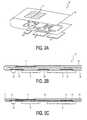
- Fig. 1ashows an assembly 1 as an illustrating example in non-assembled state.
- Assembly 1consists of a first film carrier 2 for carrying a number of integrated circuits 3 and a discrete element in the form of a capacitor 15. In this figure the circuits 3 and capacitor 15 are not yet connected to film carrier 2.
- Conducting tracks 4are arranged on film carrier 2 for connecting circuits 3 and capacitor 15.
- first film carrier 2Situated above first film carrier 2 is a second film carrier 5 which is provided with an electrical contact which is built up in this case of eight separate contact surfaces 7.
- Fig. 1bshows assembly 1 in cross-section in a situation where the integrated circuits 3 and capacitor 15 are fixedly adhered to first film carrier 2.
- first film carrier 2In first film carrier 2 are arranged openings over which tracks 4 protrude. Protruding parts 8 of tracks 4 are then urged against circuits 3 and capacitor 15 and connected thereto. Electrical couplings are thus created between circuits 3, capacitor 15 and tracks 4.
- the second film carrier 5is not yet connected to first film carrier 2.
- Assembly 1is shown in fig. 1c in fully assembled state.
- Second film carrier 5is herein connected to first film carrier 2, wherein second film carrier 5 lies against the tracks 4 of first film carrier 2.
- Tracks 4are hereby electrically insulated simultaneously. Not shown in this figure are the electrical connections which must be arranged between several of the tracks 4 and the contact surfaces 7 of electrical contact 6. Different solutions can be envisaged for this purpose. It is thus possible for instance to arrange recesses in second film carrier 5 at the position of contact surfaces 7 of electrical contact 6. Electrically conducting glue must then be placed in these openings which in the situation of the assembly 1 as shown in figure 1c lies against separate tracks 4.
- Another option for achieving an electrical connection of electrical contact 6 to tracks 4is to provide contact surfaces 7 with tracks resembling the tracks 4 on first film carrier 2.
- tracks 4 for connecting to contact surfaces 7can protrude above openings in second film carrier 5 so as to be deformed as described on the basis of the protruding parts 8 of tracks 4 with reference to fig. 1b. Through deformation the tracks can be placed into contact with tracks 4 of first film carrier 2. These bent track portions 8 can then optionally also be shielded by a filler material. Many alternatives can be envisaged by the skilled person in addition to the two described options for coupling electrical contact 6 to tracks 4.
- Fig. 2ashows an assembly 9 according to the invention in a non-assembled state which comprises only a single film carrier 10.
- the single film carrier 10is pre-folded such that an electrical contact 11 is placed opposite the mounting positions of integrated circuits 3.
- Conducting tracks 12are arranged on film carrier 10 in the same production operation as electrical contact 11.
- Fig. 2bshows a cross-section of assembly 9 in a situation where circuits 3 are mounted on film carrier 10 as described with reference to fig. 1b.
- electrical contact 11lies on the same side of the single film carrier 10 as tracks 12.
- a recessis arranged in film carrier 10 at the position of contact 11.
- the contactis hereby accessible from the top as seen in this figure.
- the advantage of placing electrical contact 11 on the shown sideis that electrical contact 11 can be manufactured with tracks 12 in one process run.
- a lacquer layer(not shown) can for instance be applied over tracks 12 and electrical contact 11.
- the figureshows an intermediate layer 13 which can be manufactured from an insulating material in order to mutually insulate contact 11 and tracks 12. It is however also possible to embody intermediate layer 13 as a conductive layer and to adhere this on both sides to film carrier 10 with for instance non-conducting glue.
- the advantage of a conductive intermediate layer 13is that an additional protection, for instance against unauthorized access, is hereby created in assembly 9.
- fig. 2cshows assembly 9 in a fully assembled state in which intermediate layer 13 is adhered on both sides to film carrier 10, electrical contact 11 and tracks 12.
- the fold 14 which results herein in film carrier 10is clearly shown. Otherwise than shown here, this fold 14 can be initiated by giving film carrier 10 a mechanically weakened form at the position of fold 14. Not shown either in this figure are the connections between electrical contact 11 and tracks 12. Reference is made therefor to the figure description of fig. 1b.
Landscapes
- Engineering & Computer Science (AREA)
- Computer Hardware Design (AREA)
- Microelectronics & Electronic Packaging (AREA)
- Physics & Mathematics (AREA)
- General Physics & Mathematics (AREA)
- Theoretical Computer Science (AREA)
- Wire Bonding (AREA)
- Coupling Device And Connection With Printed Circuit (AREA)
- Credit Cards Or The Like (AREA)
- Structures For Mounting Electric Components On Printed Circuit Boards (AREA)
Abstract
Description
- fig. 1a
- shows a perspective view of an assembly as an illustrating example prior toconstruction,
- fig. 1b
- shows a cross-section of the assembly shown in fig. 1a in a partly assembledstate,
- fig. 1c
- shows a cross-section through the assembly shown in fig. 1a and 1b in a fullyassembled state,
- fig. 2a
- is a perspective view of an assembly embodied according to the inventionin a non-assembled state,
- fig. 2b
- shows a cross-section through the assembly shown in fig. 2a in partly assembledstate with an added shield layer, and
- fig. 2c
- shows a cross-section through the assembly as shown in fig. 2b in a fullyassembled state.
Claims (8)
- Assembly (9) of at least one integrated circuit (3) and an electrical contact (11)connected to the circuit, wherein both the circuit and the electrical contact are mountedon a film carrier (10) and are mutually connected, at least in part, by means ofconducting tracks (12) which run over the film carriercharacterized in that theintegrated circuit and the electrical contact are mounted on the same film carrier (10)andin that the film carrier is folded so that it comprises stacked film carrier partscarrying the integrated circuit (3) and the electrical contact (11) respectively.
- Assembly as claimed in claim 1characterized in that an intermediate layer (13)is arranged between the stacked film carrier parts over at least part of the surface.
- Assembly as claimed in claim 1 or 2characterized in that the film carriercomprises a fold line (14) which is located between the integrated circuit (3) and theelectrical contact (11).
- Assembly as claimed in claim 3characterized in that the film carrier (10) isprovided with mechanically weakened portions at the position of the fold line (14).
- Assembly as claimed in any of the foregoing claimscharacterized in that theelectrically conducting tracks (12) run through from the one carrier part to the other andare folded together with the film carrier (10).
- Assembly as claimed in any of the foregoing claimscharacterized in that anelectrically conducting connection is formed between the stacked film carrier parts, atleast at one position, by means of an electrically conducting adhesive.
- Assembly as claimed in any of the foregoing claims,characterized in that theelectrical contact (11) consists of a number of, for instance 6 or 8, conducting contactsurfaces (7).
- Assembly as claimed in any of the foregoing claimscharacterized in that theassembly is combined with a carrier.
Applications Claiming Priority (3)
| Application Number | Priority Date | Filing Date | Title |
|---|---|---|---|
| NL1009976ANL1009976C2 (en) | 1998-08-31 | 1998-08-31 | Integrated circuit with electrical contact. |
| NL1009976 | 1998-08-31 | ||
| PCT/NL1999/000539WO2000013140A1 (en) | 1998-08-31 | 1999-08-31 | Integrated circuit with electrical contact |
Publications (2)
| Publication Number | Publication Date |
|---|---|
| EP1110175A1 EP1110175A1 (en) | 2001-06-27 |
| EP1110175B1true EP1110175B1 (en) | 2002-06-12 |
Family
ID=19767731
Family Applications (1)
| Application Number | Title | Priority Date | Filing Date |
|---|---|---|---|
| EP99941877AExpired - LifetimeEP1110175B1 (en) | 1998-08-31 | 1999-08-31 | Integrated circuit with electrical contact |
Country Status (8)
| Country | Link |
|---|---|
| EP (1) | EP1110175B1 (en) |
| AT (1) | ATE219264T1 (en) |
| AU (1) | AU5535299A (en) |
| DE (1) | DE69901844T2 (en) |
| DK (1) | DK1110175T3 (en) |
| ES (1) | ES2178464T3 (en) |
| NL (1) | NL1009976C2 (en) |
| WO (1) | WO2000013140A1 (en) |
Families Citing this family (2)
| Publication number | Priority date | Publication date | Assignee | Title |
|---|---|---|---|---|
| DE19959364A1 (en)* | 1999-12-09 | 2001-06-13 | Orga Kartensysteme Gmbh | Chip card has circuit unit electrically connected to contact areas on separate carrying body via conducting tracks in chip card body |
| DE102008053096A1 (en) | 2008-10-24 | 2010-04-29 | Giesecke & Devrient Gmbh | Method and device for the production of data carriers and semi-finished media, as well as data carriers and semi-finished media |
Family Cites Families (4)
| Publication number | Priority date | Publication date | Assignee | Title |
|---|---|---|---|---|
| US4658264A (en)* | 1984-11-09 | 1987-04-14 | Minnesota Mining And Manufacturing Company | Folded RF marker for electronic article surveillance systems |
| US5062916A (en)* | 1990-08-01 | 1991-11-05 | W. H. Brady Co. | Method for the manufacture of electrical membrane panels having circuits on flexible plastic films |
| DE4403753C1 (en)* | 1994-02-08 | 1995-07-20 | Angewandte Digital Elektronik | Combined chip card |
| FR2740582B1 (en)* | 1995-10-26 | 1997-11-28 | Gemplus Sca | HYBRID DEVICE WITH FLUSHING CONTACTS AND PRODUCING ACOUSTIC SIGNALS, AND MANUFACTURING METHOD |
- 1998
- 1998-08-31NLNL1009976Apatent/NL1009976C2/ennot_activeIP Right Cessation
- 1999
- 1999-08-31WOPCT/NL1999/000539patent/WO2000013140A1/enactiveIP Right Grant
- 1999-08-31DKDK99941877Tpatent/DK1110175T3/enactive
- 1999-08-31ESES99941877Tpatent/ES2178464T3/ennot_activeExpired - Lifetime
- 1999-08-31DEDE69901844Tpatent/DE69901844T2/ennot_activeExpired - Lifetime
- 1999-08-31ATAT99941877Tpatent/ATE219264T1/ennot_activeIP Right Cessation
- 1999-08-31AUAU55352/99Apatent/AU5535299A/ennot_activeAbandoned
- 1999-08-31EPEP99941877Apatent/EP1110175B1/ennot_activeExpired - Lifetime
Non-Patent Citations (1)
| Title |
|---|
| NAKATSUGAWA M.: "LINE-LOSS AND SIZE REDUCTION TECHNIQUES FOR MILLIMETER-WAVE RF FRONT-END BOARDS BY USING A POLYIMIDE/ALUMINA-CERAMIC MULTILAYER CONFIGURATION", IEEE TRANSACTIONS ON MICROWAVE THEORY AND TECHNIQUES, vol. 45, no. 12, 1 December 1997 (1997-12-01), pages 2308 - 2315, XP000732014* |
Also Published As
| Publication number | Publication date |
|---|---|
| ES2178464T3 (en) | 2002-12-16 |
| ATE219264T1 (en) | 2002-06-15 |
| WO2000013140A1 (en) | 2000-03-09 |
| DE69901844D1 (en) | 2002-07-18 |
| DE69901844T2 (en) | 2003-01-09 |
| DK1110175T3 (en) | 2002-09-16 |
| AU5535299A (en) | 2000-03-21 |
| NL1009976C2 (en) | 2000-03-02 |
| EP1110175A1 (en) | 2001-06-27 |
Similar Documents
| Publication | Publication Date | Title |
|---|---|---|
| US6568600B1 (en) | Chip card equipped with a loop antenna, and associated micromodule | |
| US4195195A (en) | Tape automated bonding test board | |
| US4975761A (en) | High performance plastic encapsulated package for integrated circuit die | |
| US5016085A (en) | Hermetic package for integrated circuit chips | |
| US5018051A (en) | IC card having circuit modules for mounting electronic components | |
| US20040159955A1 (en) | Semiconductor chip module | |
| CN1427982B (en) | Smart card | |
| US4931908A (en) | Housing for an electronic circuit | |
| US6384425B1 (en) | Nonconductive substrate forming a strip or a panel on which a multiplicity of carrier elements is formed | |
| WO1996015555A1 (en) | Multi-layer lead frame for a semiconductor device | |
| US5311396A (en) | Smart card chip-based electronic circuit | |
| US6307255B1 (en) | Multi-layer lead frame for a semiconductor device | |
| CA2705619C (en) | Device for protecting the pins of an electronic component | |
| US4599486A (en) | High capacitance bus bar including multilayer ceramic capacitors | |
| JP2821315B2 (en) | Single inline module | |
| JPH01261849A (en) | Semiconductor device | |
| US5583748A (en) | Semiconductor module having multiple circuit boards | |
| EP1110175B1 (en) | Integrated circuit with electrical contact | |
| US5708568A (en) | Electronic module with low impedance ground connection using flexible circuits | |
| EP0262493B1 (en) | Electronic package with distributed decoupling capacitors | |
| JPH0655554B2 (en) | IC card and method of manufacturing the same | |
| RU2032964C1 (en) | Device on integrated circuits | |
| JP2002207982A (en) | Contactless and non-contact IC module and IC card | |
| JPS5944798B2 (en) | Wiring device for electronic components | |
| JP2823279B2 (en) | Card-shaped electronic device and method of manufacturing the same |
Legal Events
| Date | Code | Title | Description |
|---|---|---|---|
| PUAI | Public reference made under article 153(3) epc to a published international application that has entered the european phase | Free format text:ORIGINAL CODE: 0009012 | |
| 17P | Request for examination filed | Effective date:20010402 | |
| AK | Designated contracting states | Kind code of ref document:A1 Designated state(s):AT BE CH CY DE DK ES FI FR GB GR IE IT LI LU MC NL PT SE | |
| AX | Request for extension of the european patent | Free format text:AL;LT;LV;MK;RO;SI | |
| GRAG | Despatch of communication of intention to grant | Free format text:ORIGINAL CODE: EPIDOS AGRA | |
| 17Q | First examination report despatched | Effective date:20010723 | |
| GRAG | Despatch of communication of intention to grant | Free format text:ORIGINAL CODE: EPIDOS AGRA | |
| GRAH | Despatch of communication of intention to grant a patent | Free format text:ORIGINAL CODE: EPIDOS IGRA | |
| GRAH | Despatch of communication of intention to grant a patent | Free format text:ORIGINAL CODE: EPIDOS IGRA | |
| GRAA | (expected) grant | Free format text:ORIGINAL CODE: 0009210 | |
| AK | Designated contracting states | Kind code of ref document:B1 Designated state(s):AT BE CH CY DE DK ES FI FR GB GR IE IT LI LU MC NL PT SE | |
| PG25 | Lapsed in a contracting state [announced via postgrant information from national office to epo] | Ref country code:LI Free format text:LAPSE BECAUSE OF FAILURE TO SUBMIT A TRANSLATION OF THE DESCRIPTION OR TO PAY THE FEE WITHIN THE PRESCRIBED TIME-LIMIT Effective date:20020612 Ref country code:GR Free format text:LAPSE BECAUSE OF FAILURE TO SUBMIT A TRANSLATION OF THE DESCRIPTION OR TO PAY THE FEE WITHIN THE PRESCRIBED TIME-LIMIT Effective date:20020612 Ref country code:CH Free format text:LAPSE BECAUSE OF FAILURE TO SUBMIT A TRANSLATION OF THE DESCRIPTION OR TO PAY THE FEE WITHIN THE PRESCRIBED TIME-LIMIT Effective date:20020612 Ref country code:AT Free format text:LAPSE BECAUSE OF FAILURE TO SUBMIT A TRANSLATION OF THE DESCRIPTION OR TO PAY THE FEE WITHIN THE PRESCRIBED TIME-LIMIT Effective date:20020612 | |
| REF | Corresponds to: | Ref document number:219264 Country of ref document:AT Date of ref document:20020615 Kind code of ref document:T | |
| REG | Reference to a national code | Ref country code:GB Ref legal event code:FG4D | |
| REG | Reference to a national code | Ref country code:CH Ref legal event code:EP | |
| REF | Corresponds to: | Ref document number:69901844 Country of ref document:DE Date of ref document:20020718 | |
| REG | Reference to a national code | Ref country code:IE Ref legal event code:FG4D | |
| PG25 | Lapsed in a contracting state [announced via postgrant information from national office to epo] | Ref country code:LU Free format text:LAPSE BECAUSE OF NON-PAYMENT OF DUE FEES Effective date:20020831 Ref country code:CY Free format text:LAPSE BECAUSE OF FAILURE TO SUBMIT A TRANSLATION OF THE DESCRIPTION OR TO PAY THE FEE WITHIN THE PRESCRIBED TIME-LIMIT Effective date:20020831 | |
| PG25 | Lapsed in a contracting state [announced via postgrant information from national office to epo] | Ref country code:PT Free format text:LAPSE BECAUSE OF FAILURE TO SUBMIT A TRANSLATION OF THE DESCRIPTION OR TO PAY THE FEE WITHIN THE PRESCRIBED TIME-LIMIT Effective date:20020916 | |
| REG | Reference to a national code | Ref country code:DK Ref legal event code:T3 | |
| ET | Fr: translation filed | ||
| REG | Reference to a national code | Ref country code:ES Ref legal event code:FG2A Ref document number:2178464 Country of ref document:ES Kind code of ref document:T3 | |
| REG | Reference to a national code | Ref country code:CH Ref legal event code:PL | |
| PG25 | Lapsed in a contracting state [announced via postgrant information from national office to epo] | Ref country code:MC Free format text:LAPSE BECAUSE OF NON-PAYMENT OF DUE FEES Effective date:20030301 | |
| PLBE | No opposition filed within time limit | Free format text:ORIGINAL CODE: 0009261 | |
| STAA | Information on the status of an ep patent application or granted ep patent | Free format text:STATUS: NO OPPOSITION FILED WITHIN TIME LIMIT | |
| 26N | No opposition filed | Effective date:20030313 | |
| REG | Reference to a national code | Ref country code:GB Ref legal event code:732E | |
| NLS | Nl: assignments of ep-patents | Owner name:SYNTIQ INTERNATIONAL B.V. | |
| REG | Reference to a national code | Ref country code:ES Ref legal event code:PC2A | |
| REG | Reference to a national code | Ref country code:FR Ref legal event code:TP | |
| PG25 | Lapsed in a contracting state [announced via postgrant information from national office to epo] | Ref country code:IT Free format text:LAPSE BECAUSE OF NON-PAYMENT OF DUE FEES Effective date:20050831 | |
| PGFP | Annual fee paid to national office [announced via postgrant information from national office to epo] | Ref country code:NL Payment date:20100826 Year of fee payment:12 Ref country code:IE Payment date:20100831 Year of fee payment:12 Ref country code:ES Payment date:20100826 Year of fee payment:12 | |
| PGFP | Annual fee paid to national office [announced via postgrant information from national office to epo] | Ref country code:SE Payment date:20100826 Year of fee payment:12 Ref country code:FR Payment date:20100831 Year of fee payment:12 Ref country code:FI Payment date:20100820 Year of fee payment:12 | |
| PGFP | Annual fee paid to national office [announced via postgrant information from national office to epo] | Ref country code:GB Payment date:20100803 Year of fee payment:12 | |
| PGFP | Annual fee paid to national office [announced via postgrant information from national office to epo] | Ref country code:DK Payment date:20100813 Year of fee payment:12 | |
| PGFP | Annual fee paid to national office [announced via postgrant information from national office to epo] | Ref country code:DE Payment date:20101029 Year of fee payment:12 Ref country code:BE Payment date:20100826 Year of fee payment:12 | |
| PGFP | Annual fee paid to national office [announced via postgrant information from national office to epo] | Ref country code:IT Payment date:20100708 Year of fee payment:12 | |
| PGRI | Patent reinstated in contracting state [announced from national office to epo] | Ref country code:IT Effective date:20110616 | |
| BERE | Be: lapsed | Owner name:*SYNTIQ INTERNATIONAL B.V. Effective date:20110831 | |
| REG | Reference to a national code | Ref country code:NL Ref legal event code:V1 Effective date:20120301 | |
| GBPC | Gb: european patent ceased through non-payment of renewal fee | Effective date:20110831 | |
| REG | Reference to a national code | Ref country code:DK Ref legal event code:EBP | |
| REG | Reference to a national code | Ref country code:FR Ref legal event code:ST Effective date:20120430 | |
| REG | Reference to a national code | Ref country code:IE Ref legal event code:MM4A | |
| PG25 | Lapsed in a contracting state [announced via postgrant information from national office to epo] | Ref country code:BE Free format text:LAPSE BECAUSE OF NON-PAYMENT OF DUE FEES Effective date:20110831 Ref country code:NL Free format text:LAPSE BECAUSE OF NON-PAYMENT OF DUE FEES Effective date:20120301 Ref country code:IT Free format text:LAPSE BECAUSE OF NON-PAYMENT OF DUE FEES Effective date:20110831 Ref country code:FI Free format text:LAPSE BECAUSE OF NON-PAYMENT OF DUE FEES Effective date:20110831 | |
| REG | Reference to a national code | Ref country code:DE Ref legal event code:R119 Ref document number:69901844 Country of ref document:DE Effective date:20120301 | |
| REG | Reference to a national code | Ref country code:SE Ref legal event code:EUG | |
| PG25 | Lapsed in a contracting state [announced via postgrant information from national office to epo] | Ref country code:DK Free format text:LAPSE BECAUSE OF NON-PAYMENT OF DUE FEES Effective date:20110831 Ref country code:IE Free format text:LAPSE BECAUSE OF NON-PAYMENT OF DUE FEES Effective date:20110831 | |
| PG25 | Lapsed in a contracting state [announced via postgrant information from national office to epo] | Ref country code:FR Free format text:LAPSE BECAUSE OF NON-PAYMENT OF DUE FEES Effective date:20110831 Ref country code:GB Free format text:LAPSE BECAUSE OF NON-PAYMENT OF DUE FEES Effective date:20110831 | |
| PG25 | Lapsed in a contracting state [announced via postgrant information from national office to epo] | Ref country code:SE Free format text:LAPSE BECAUSE OF NON-PAYMENT OF DUE FEES Effective date:20110901 | |
| REG | Reference to a national code | Ref country code:ES Ref legal event code:FD2A Effective date:20130606 | |
| PG25 | Lapsed in a contracting state [announced via postgrant information from national office to epo] | Ref country code:DE Free format text:LAPSE BECAUSE OF NON-PAYMENT OF DUE FEES Effective date:20120301 | |
| PG25 | Lapsed in a contracting state [announced via postgrant information from national office to epo] | Ref country code:ES Free format text:LAPSE BECAUSE OF NON-PAYMENT OF DUE FEES Effective date:20110901 |