EP1098000A2 - Embedded metallic deposits forming an electrode set for an electrochemical sensor strip - Google Patents
Embedded metallic deposits forming an electrode set for an electrochemical sensor stripDownload PDFInfo
- Publication number
- EP1098000A2 EP1098000A2EP00123693AEP00123693AEP1098000A2EP 1098000 A2EP1098000 A2EP 1098000A2EP 00123693 AEP00123693 AEP 00123693AEP 00123693 AEP00123693 AEP 00123693AEP 1098000 A2EP1098000 A2EP 1098000A2
- Authority
- EP
- European Patent Office
- Prior art keywords
- pattern
- substrate
- metallic deposits
- electrode
- metallic
- Prior art date
- Legal status (The legal status is an assumption and is not a legal conclusion. Google has not performed a legal analysis and makes no representation as to the accuracy of the status listed.)
- Withdrawn
Links
- 239000000758substrateSubstances0.000claimsabstractdescription73
- 238000001746injection mouldingMethods0.000claimsabstractdescription12
- 238000004519manufacturing processMethods0.000claimsabstractdescription4
- 229910052751metalInorganic materials0.000claimsdescription17
- 239000002184metalSubstances0.000claimsdescription17
- 238000000034methodMethods0.000claimsdescription17
- KDLHZDBZIXYQEI-UHFFFAOYSA-NPalladiumChemical compound[Pd]KDLHZDBZIXYQEI-UHFFFAOYSA-N0.000claimsdescription14
- BASFCYQUMIYNBI-UHFFFAOYSA-NplatinumChemical compound[Pt]BASFCYQUMIYNBI-UHFFFAOYSA-N0.000claimsdescription14
- 229920000642polymerPolymers0.000claimsdescription14
- 229920001169thermoplasticPolymers0.000claimsdescription12
- PCHJSUWPFVWCPO-UHFFFAOYSA-NgoldChemical compound[Au]PCHJSUWPFVWCPO-UHFFFAOYSA-N0.000claimsdescription10
- 229910052737goldInorganic materials0.000claimsdescription10
- 239000010931goldSubstances0.000claimsdescription10
- 239000004417polycarbonateSubstances0.000claimsdescription9
- 229920000515polycarbonatePolymers0.000claimsdescription9
- 229910052741iridiumInorganic materials0.000claimsdescription7
- GKOZUEZYRPOHIO-UHFFFAOYSA-Niridium atomChemical compound[Ir]GKOZUEZYRPOHIO-UHFFFAOYSA-N0.000claimsdescription7
- 229910052763palladiumInorganic materials0.000claimsdescription7
- 229910052697platinumInorganic materials0.000claimsdescription7
- 239000010410layerSubstances0.000description25
- 239000000463materialSubstances0.000description22
- 239000000523sampleSubstances0.000description11
- 239000003153chemical reaction reagentSubstances0.000description10
- -1polyethylenePolymers0.000description9
- 239000000956alloySubstances0.000description6
- 229910045601alloyInorganic materials0.000description6
- 238000007650screen-printingMethods0.000description6
- 239000000853adhesiveSubstances0.000description5
- 230000001070adhesive effectEffects0.000description5
- 238000002347injectionMethods0.000description5
- 239000007924injectionSubstances0.000description5
- 229920002120photoresistant polymerPolymers0.000description5
- 239000002904solventSubstances0.000description5
- RYGMFSIKBFXOCR-UHFFFAOYSA-NCopperChemical compound[Cu]RYGMFSIKBFXOCR-UHFFFAOYSA-N0.000description4
- PXHVJJICTQNCMI-UHFFFAOYSA-NNickelChemical compound[Ni]PXHVJJICTQNCMI-UHFFFAOYSA-N0.000description4
- 230000015572biosynthetic processEffects0.000description4
- 229910052802copperInorganic materials0.000description4
- 239000010949copperSubstances0.000description4
- 239000000203mixtureSubstances0.000description4
- 239000000178monomerSubstances0.000description4
- 238000000465mouldingMethods0.000description4
- 239000012704polymeric precursorSubstances0.000description4
- 239000004416thermosoftening plasticSubstances0.000description4
- 108090000790EnzymesProteins0.000description3
- 102000004190EnzymesHuman genes0.000description3
- 150000002739metalsChemical class0.000description3
- 238000003801millingMethods0.000description3
- OKTJSMMVPCPJKN-UHFFFAOYSA-NCarbonChemical compound[C]OKTJSMMVPCPJKN-UHFFFAOYSA-N0.000description2
- XEEYBQQBJWHFJM-UHFFFAOYSA-NIronChemical compound[Fe]XEEYBQQBJWHFJM-UHFFFAOYSA-N0.000description2
- 239000004743PolypropyleneSubstances0.000description2
- XUIMIQQOPSSXEZ-UHFFFAOYSA-NSiliconChemical compound[Si]XUIMIQQOPSSXEZ-UHFFFAOYSA-N0.000description2
- RTAQQCXQSZGOHL-UHFFFAOYSA-NTitaniumChemical compound[Ti]RTAQQCXQSZGOHL-UHFFFAOYSA-N0.000description2
- 239000012491analyteSubstances0.000description2
- 239000008280bloodSubstances0.000description2
- 210000004369bloodAnatomy0.000description2
- 239000000919ceramicSubstances0.000description2
- 239000004020conductorSubstances0.000description2
- 230000007613environmental effectEffects0.000description2
- 229920005570flexible polymerPolymers0.000description2
- 239000012530fluidSubstances0.000description2
- 239000011888foilSubstances0.000description2
- 108010054770glucose dehydrogenase (pyrroloquinoline-quinone)Proteins0.000description2
- 239000007788liquidSubstances0.000description2
- 229910052759nickelInorganic materials0.000description2
- 229910000510noble metalInorganic materials0.000description2
- 229920000728polyesterPolymers0.000description2
- 229920001155polypropylenePolymers0.000description2
- 239000012779reinforcing materialSubstances0.000description2
- 229910052710siliconInorganic materials0.000description2
- 239000010703siliconSubstances0.000description2
- 239000000243solutionSubstances0.000description2
- 239000000126substanceSubstances0.000description2
- 239000004094surface-active agentSubstances0.000description2
- 229910052719titaniumInorganic materials0.000description2
- 239000010936titaniumSubstances0.000description2
- WFKWXMTUELFFGS-UHFFFAOYSA-NtungstenChemical compound[W]WFKWXMTUELFFGS-UHFFFAOYSA-N0.000description2
- 229910052721tungstenInorganic materials0.000description2
- 239000010937tungstenSubstances0.000description2
- 238000003466weldingMethods0.000description2
- 238000007704wet chemistry methodMethods0.000description2
- HDTRYLNUVZCQOY-UHFFFAOYSA-Nα-D-glucopyranosyl-α-D-glucopyranosideNatural productsOC1C(O)C(O)C(CO)OC1OC1C(O)C(O)C(O)C(CO)O1HDTRYLNUVZCQOY-UHFFFAOYSA-N0.000description1
- 229910000497AmalgamInorganic materials0.000description1
- 108010006591ApoenzymesProteins0.000description1
- GYHNNYVSQQEPJS-UHFFFAOYSA-NGalliumChemical compound[Ga]GYHNNYVSQQEPJS-UHFFFAOYSA-N0.000description1
- WQZGKKKJIJFFOK-GASJEMHNSA-NGlucoseNatural productsOC[C@H]1OC(O)[C@H](O)[C@@H](O)[C@@H]1OWQZGKKKJIJFFOK-GASJEMHNSA-N0.000description1
- 229920000663Hydroxyethyl cellulosePolymers0.000description1
- FYYHWMGAXLPEAU-UHFFFAOYSA-NMagnesiumChemical compound[Mg]FYYHWMGAXLPEAU-UHFFFAOYSA-N0.000description1
- 239000004677NylonSubstances0.000description1
- 229920003171Poly (ethylene oxide)Polymers0.000description1
- 239000004698PolyethyleneSubstances0.000description1
- 239000004642PolyimideSubstances0.000description1
- 239000004721Polyphenylene oxideSubstances0.000description1
- 239000004793PolystyreneSubstances0.000description1
- BUGBHKTXTAQXES-UHFFFAOYSA-NSeleniumChemical compound[Se]BUGBHKTXTAQXES-UHFFFAOYSA-N0.000description1
- BQCADISMDOOEFD-UHFFFAOYSA-NSilverChemical compound[Ag]BQCADISMDOOEFD-UHFFFAOYSA-N0.000description1
- ATJFFYVFTNAWJD-UHFFFAOYSA-NTinChemical compound[Sn]ATJFFYVFTNAWJD-UHFFFAOYSA-N0.000description1
- HDTRYLNUVZCQOY-WSWWMNSNSA-NTrehaloseNatural productsO[C@@H]1[C@@H](O)[C@@H](O)[C@@H](CO)O[C@@H]1O[C@@H]1[C@H](O)[C@@H](O)[C@@H](O)[C@@H](CO)O1HDTRYLNUVZCQOY-WSWWMNSNSA-N0.000description1
- 229910052770UraniumInorganic materials0.000description1
- HCHKCACWOHOZIP-UHFFFAOYSA-NZincChemical compound[Zn]HCHKCACWOHOZIP-UHFFFAOYSA-N0.000description1
- QCWXUUIWCKQGHC-UHFFFAOYSA-NZirconiumChemical compound[Zr]QCWXUUIWCKQGHC-UHFFFAOYSA-N0.000description1
- DHKHKXVYLBGOIT-UHFFFAOYSA-Nacetaldehyde Diethyl AcetalNatural productsCCOC(C)OCCDHKHKXVYLBGOIT-UHFFFAOYSA-N0.000description1
- 150000001241acetalsChemical class0.000description1
- NIXOWILDQLNWCW-UHFFFAOYSA-Nacrylic acid groupChemical groupC(C=C)(=O)ONIXOWILDQLNWCW-UHFFFAOYSA-N0.000description1
- 239000004676acrylonitrile butadiene styreneSubstances0.000description1
- 238000004026adhesive bondingMethods0.000description1
- HDTRYLNUVZCQOY-LIZSDCNHSA-Nalpha,alpha-trehaloseChemical compoundO[C@@H]1[C@@H](O)[C@H](O)[C@@H](CO)O[C@@H]1O[C@@H]1[C@H](O)[C@@H](O)[C@H](O)[C@@H](CO)O1HDTRYLNUVZCQOY-LIZSDCNHSA-N0.000description1
- 229910052782aluminiumInorganic materials0.000description1
- XAGFODPZIPBFFR-UHFFFAOYSA-NaluminiumChemical compound[Al]XAGFODPZIPBFFR-UHFFFAOYSA-N0.000description1
- 239000007864aqueous solutionSubstances0.000description1
- QVGXLLKOCUKJST-UHFFFAOYSA-Natomic oxygenChemical compound[O]QVGXLLKOCUKJST-UHFFFAOYSA-N0.000description1
- 239000012472biological sampleSubstances0.000description1
- 229910052799carbonInorganic materials0.000description1
- 239000003795chemical substances by applicationSubstances0.000description1
- 229910017052cobaltInorganic materials0.000description1
- 239000010941cobaltSubstances0.000description1
- GUTLYIVDDKVIGB-UHFFFAOYSA-Ncobalt atomChemical compound[Co]GUTLYIVDDKVIGB-UHFFFAOYSA-N0.000description1
- 150000001875compoundsChemical class0.000description1
- 229920001577copolymerPolymers0.000description1
- 230000007547defectEffects0.000description1
- 230000000994depressogenic effectEffects0.000description1
- 229940111685dibasic potassium phosphateDrugs0.000description1
- ZPWVASYFFYYZEW-UHFFFAOYSA-Ldipotassium hydrogen phosphateChemical compound[K+].[K+].OP([O-])([O-])=OZPWVASYFFYYZEW-UHFFFAOYSA-L0.000description1
- 230000000694effectsEffects0.000description1
- 230000005611electricityEffects0.000description1
- 238000005323electroformingMethods0.000description1
- 239000003792electrolyteSubstances0.000description1
- 230000008030eliminationEffects0.000description1
- 238000003379elimination reactionMethods0.000description1
- 229920006351engineering plasticPolymers0.000description1
- 238000005530etchingMethods0.000description1
- 230000008020evaporationEffects0.000description1
- 238000001704evaporationMethods0.000description1
- 238000010304firingMethods0.000description1
- 229910052733galliumInorganic materials0.000description1
- 239000007789gasSubstances0.000description1
- 239000011521glassSubstances0.000description1
- 239000003365glass fiberSubstances0.000description1
- 239000008103glucoseSubstances0.000description1
- 239000010439graphiteSubstances0.000description1
- 229910002804graphiteInorganic materials0.000description1
- 239000003779heat-resistant materialSubstances0.000description1
- 235000019447hydroxyethyl celluloseNutrition0.000description1
- 229910052738indiumInorganic materials0.000description1
- APFVFJFRJDLVQX-UHFFFAOYSA-Nindium atomChemical compound[In]APFVFJFRJDLVQX-UHFFFAOYSA-N0.000description1
- 229910052742ironInorganic materials0.000description1
- 230000001788irregularEffects0.000description1
- 238000000608laser ablationMethods0.000description1
- 239000011133leadSubstances0.000description1
- 238000001459lithographyMethods0.000description1
- 229910052749magnesiumInorganic materials0.000description1
- 239000011777magnesiumSubstances0.000description1
- 238000005259measurementMethods0.000description1
- QSHDDOUJBYECFT-UHFFFAOYSA-NmercuryChemical compound[Hg]QSHDDOUJBYECFT-UHFFFAOYSA-N0.000description1
- 229910052753mercuryInorganic materials0.000description1
- 239000007769metal materialSubstances0.000description1
- 238000000520microinjectionMethods0.000description1
- 238000012986modificationMethods0.000description1
- 230000004048modificationEffects0.000description1
- 229940111688monobasic potassium phosphateDrugs0.000description1
- 235000019796monopotassium phosphateNutrition0.000description1
- 229910052758niobiumInorganic materials0.000description1
- 239000010955niobiumSubstances0.000description1
- GUCVJGMIXFAOAE-UHFFFAOYSA-Nniobium atomChemical compound[Nb]GUCVJGMIXFAOAE-UHFFFAOYSA-N0.000description1
- 229920001778nylonPolymers0.000description1
- 229910052762osmiumInorganic materials0.000description1
- SYQBFIAQOQZEGI-UHFFFAOYSA-Nosmium atomChemical compound[Os]SYQBFIAQOQZEGI-UHFFFAOYSA-N0.000description1
- 229910052760oxygenInorganic materials0.000description1
- 239000001301oxygenSubstances0.000description1
- 238000005240physical vapour depositionMethods0.000description1
- 238000005498polishingMethods0.000description1
- 229920003229poly(methyl methacrylate)Polymers0.000description1
- 229920002492poly(sulfone)Polymers0.000description1
- 229910021420polycrystalline siliconInorganic materials0.000description1
- 229920000573polyethylenePolymers0.000description1
- 229920001721polyimidePolymers0.000description1
- 239000002861polymer materialSubstances0.000description1
- 238000006116polymerization reactionMethods0.000description1
- 229920000193polymethacrylatePolymers0.000description1
- 239000004926polymethyl methacrylateSubstances0.000description1
- 229920006380polyphenylene oxidePolymers0.000description1
- 229920002223polystyrenePolymers0.000description1
- 239000004800polyvinyl chlorideSubstances0.000description1
- 229920000915polyvinyl chloridePolymers0.000description1
- GNSKLFRGEWLPPA-UHFFFAOYSA-Mpotassium dihydrogen phosphateChemical compound[K+].OP(O)([O-])=OGNSKLFRGEWLPPA-UHFFFAOYSA-M0.000description1
- MMXZSJMASHPLLR-UHFFFAOYSA-Npyrroloquinoline quinoneChemical compoundC12=C(C(O)=O)C=C(C(O)=O)N=C2C(=O)C(=O)C2=C1NC(C(=O)O)=C2MMXZSJMASHPLLR-UHFFFAOYSA-N0.000description1
- 239000000376reactantSubstances0.000description1
- 238000010107reaction injection mouldingMethods0.000description1
- 238000010133reinforced reaction injection mouldingMethods0.000description1
- 239000012783reinforcing fiberSubstances0.000description1
- 229910052702rheniumInorganic materials0.000description1
- WUAPFZMCVAUBPE-UHFFFAOYSA-Nrhenium atomChemical compound[Re]WUAPFZMCVAUBPE-UHFFFAOYSA-N0.000description1
- 229910052703rhodiumInorganic materials0.000description1
- 239000010948rhodiumSubstances0.000description1
- MHOVAHRLVXNVSD-UHFFFAOYSA-Nrhodium atomChemical compound[Rh]MHOVAHRLVXNVSD-UHFFFAOYSA-N0.000description1
- 229910052711seleniumInorganic materials0.000description1
- 239000011669seleniumSubstances0.000description1
- 229910052709silverInorganic materials0.000description1
- 239000004332silverSubstances0.000description1
- 239000002356single layerSubstances0.000description1
- 229940074404sodium succinateDrugs0.000description1
- ZDQYSKICYIVCPN-UHFFFAOYSA-Lsodium succinate (anhydrous)Chemical compound[Na+].[Na+].[O-]C(=O)CCC([O-])=OZDQYSKICYIVCPN-UHFFFAOYSA-L0.000description1
- 239000007787solidSubstances0.000description1
- 239000011343solid materialSubstances0.000description1
- 238000004544sputter depositionMethods0.000description1
- 229910052715tantalumInorganic materials0.000description1
- GUVRBAGPIYLISA-UHFFFAOYSA-Ntantalum atomChemical compound[Ta]GUVRBAGPIYLISA-UHFFFAOYSA-N0.000description1
- 229920001187thermosetting polymerPolymers0.000description1
- 239000004634thermosetting polymerSubstances0.000description1
- 229910052718tinInorganic materials0.000description1
- 239000011135tinSubstances0.000description1
- GPRLSGONYQIRFK-MNYXATJNSA-NtritonChemical compound[3H+]GPRLSGONYQIRFK-MNYXATJNSA-N0.000description1
- DNYWZCXLKNTFFI-UHFFFAOYSA-NuraniumChemical compound[U][U][U][U][U][U][U][U][U][U][U][U][U][U][U][U][U][U][U][U][U][U][U][U][U][U][U][U][U][U][U][U][U][U][U][U][U][U][U][U][U][U][U][U][U][U][U][U][U][U][U][U][U][U][U][U][U][U][U][U][U][U][U][U][U][U][U][U][U][U][U][U][U][U][U][U][U][U][U][U][U][U][U][U][U][U][U][U][U][U][U][U][U][U][U][U][U][U][U][U][U][U][U][U][U][U][U][U][U][U][U][U][U][U]DNYWZCXLKNTFFI-UHFFFAOYSA-N0.000description1
- 229910052720vanadiumInorganic materials0.000description1
- GPPXJZIENCGNKB-UHFFFAOYSA-NvanadiumChemical compound[V]#[V]GPPXJZIENCGNKB-UHFFFAOYSA-N0.000description1
- 229910052725zincInorganic materials0.000description1
- 239000011701zincSubstances0.000description1
- 229910052726zirconiumInorganic materials0.000description1
Images


Classifications
- G—PHYSICS
- G01—MEASURING; TESTING
- G01N—INVESTIGATING OR ANALYSING MATERIALS BY DETERMINING THEIR CHEMICAL OR PHYSICAL PROPERTIES
- G01N27/00—Investigating or analysing materials by the use of electric, electrochemical, or magnetic means
- G01N27/26—Investigating or analysing materials by the use of electric, electrochemical, or magnetic means by investigating electrochemical variables; by using electrolysis or electrophoresis
- G01N27/403—Cells and electrode assemblies
- H—ELECTRICITY
- H05—ELECTRIC TECHNIQUES NOT OTHERWISE PROVIDED FOR
- H05K—PRINTED CIRCUITS; CASINGS OR CONSTRUCTIONAL DETAILS OF ELECTRIC APPARATUS; MANUFACTURE OF ASSEMBLAGES OF ELECTRICAL COMPONENTS
- H05K3/00—Apparatus or processes for manufacturing printed circuits
- H05K3/02—Apparatus or processes for manufacturing printed circuits in which the conductive material is applied to the surface of the insulating support and is thereafter removed from such areas of the surface which are not intended for current conducting or shielding
- H05K3/04—Apparatus or processes for manufacturing printed circuits in which the conductive material is applied to the surface of the insulating support and is thereafter removed from such areas of the surface which are not intended for current conducting or shielding the conductive material being removed mechanically, e.g. by punching
- H05K3/045—Apparatus or processes for manufacturing printed circuits in which the conductive material is applied to the surface of the insulating support and is thereafter removed from such areas of the surface which are not intended for current conducting or shielding the conductive material being removed mechanically, e.g. by punching by making a conductive layer having a relief pattern, followed by abrading of the raised portions
Definitions
- the present inventionrelates to embedded metallic deposits.
- Electrochemical biosensorsare well known. They have been used to determine the concentration of various analytes from biological samples, particularly from blood. Electrochemical biosensors are described in U.S. Patent Nos. 5,413,690; 5,762,770 and 5,798,031; as well as in International Publication No. WO99/13101, each of which are hereby incorporated by reference.
- An electrochemical biosensortypically includes a sensor strip.
- the sensor stripincludes a space that holds the sample to be analyzed, may include reagents to be released into the sample, and includes an electrode set.
- the electrode setnormally includes an insulating substrate, electrodes that contact the sample, which have contact pads for electrically connecting the electrodes to the electronics of the electrochemical biosensor.
- electrochemical biosensorsit is desirable for electrochemical biosensors to be able to analyze electrolytes using as small a sample as possible, and therefore it is necessary to miniaturize the sensor strip, as well as its parts, including the electrodes, as much as possible.
- screen printing techniqueshave been used to form miniaturized electrodes.
- Electrodes formed by screen printing techniquescan only be formed from compositions that are both electrically conductive and which are screen printable. Furthermore, screen printing techniques are typically only reliable when forming structures and patterns having a feature size of approximately 75 ⁇ m or greater. In addition, screen printing is a wet chemical process, with attendant processing and environmental costs. It would be desirable to have a new method of forming electrodes which allows for the use of different compositions, which can form features smaller than 75 ⁇ m, and does not require a wet chemical process.
- Injection moldingis a technique used to make shaped parts from many polymeric materials. Usually, a molten thermoplastic polymer is forced into a two-part mold. The thermoplastic cools and hardens, taking on the shape of the mold.
- a type of injection moldingknown as reaction injection molding (RIM) is carried out using monomers or low-molecular weight polymeric precursors of a thermosetting polymer; the monomers or polymeric precursors are rapidly mixed and injected into the mold as the polymerization process takes place.
- reinforcing fibersmay also be injected along with the monomers or polymeric precursors, in a process known as reinforced reaction injection molding (RRIM).
- Injection moldingcan be used to form very fine structures, such as the data encoding portions of compact discs; this type of injection molding is often referred to as microinjection molding.
- the inventionis a set of metallic deposits, comprising a pattern of channels in a surface of a substrate, and metallic deposits in the pattern. Portions of the surface are exposed, and the substrate comprises a polymer.
- the inventionis an electrode set, comprising an electrode pattern in a surface of a substrate, and metallic deposits in the pattern.
- the substratecomprises a polymer.
- the inventionis a method of making a set of metallic deposits, comprising injection molding a substrate, where a pattern of channels is in a surface of the substrate, applying a metallic layer on the surface, to form metallic deposits in the pattern, and removing a portion of the metallic layer, to expose a portion of the surface.
- the inventionis a mold insert, comprising a metal, where a reverse electrode pattern is in a surface of the mold insert.
- An advantage of the present inventionis that it allows for the possibility of small feature sizes.
- patternmeans one or more intentionally formed channels or raised ridges having a feature size, for example, a single linear channel having a constant width, where the smallest width is the feature size. Not included in the term “pattern” are natural, unintentional defects.
- channelrefers to a portion of the surface that is depressed relative to adjacent portions of the surface.
- pattern of channelsrefers to a pattern formed of one or more channels.
- a pattern of channelshas two parts: the channel or channels, and the remaining parts of the pattern, referred to as an "island" or "islands”.
- feature sizeis the smallest width of a channel or raised ridge found in a pattern.
- electrode patternis a pattern of channels, which when filled with a metallic material includes at least two, for example 2 to 60, or 3 to 20, electrodes which are not electrically connected to each other, but each of which includes its own contact pad.
- a "reverse electrode pattern”is the negative impression of an electrode pattern, i.e., where an electrode pattern has channels, a reverse electrode pattern has raised ridges.
- injection moldable polymerrefers to a polymer which can be formed by an injection molding process, and includes not only thermoplastic polymers, but also polymer which are synthesized during the forming process, i.e., polymers formed by during reactive injection molding.
- metal channelrefers to a channel filled with a material that is a metallic conductor of electricity, such as a pure metal or alloy.
- electrode setis a set of at least two electrodes, for example 2 to 60, or 3 to 20, electrodes. These electrodes may be, for example, a working electrode, a reference electrode, and/or a counter electrode.
- Figures 1 to 4illustrate how a substrate mold insert is made.
- Figures 5 to 7illustrate how an electrode set is made.
- Figures 8 to 10illustrate how a lid is made.
- Figures 11 and 12illustrate how a sensor is made.
- Figure 1illustrates a master mold blank 2 , including a surface 4 with a layer of photoresist 6 on the surface.
- a pattern of channelssuch as an electrode pattern, is then formed in the photoresist layer by exposing and developing the photoresist using a mask.
- the resulting pattern 12 in the photoresist 6 , on the surface 4forms a master mold 8 , illustrated in Figure 2.
- the surfacemay be made from any solid material, including glass, silicon, metal or a polymer. Either a negative or positive photoresist may be used.
- Figure 3illustrates the master mold 8 covered with a thick material layer, to form the substrate mold insert 10 .
- the thick material that forms the substrate mold insertmay be made of any heat resistant material which will tolerate the conditions inside the mold during injection molding. Examples include metals, such as copper, nickel, or gold.
- the thick material layermay be formed by electroforming or physical vapor deposition, or in the case of a ceramic, by pressure application to form a green body. In the case of a ceramic, the substrate mold insert may be fired before use, and dimensional changes resulting from firing can be compensated beforehand by selecting the original dimensions of the master mold.
- Figure 4illustrates the substrate mold insert 10 , having a negative image of the pattern 14 , i.e., in the case of an electrode pattern, the negative image will be a reverse electrode pattern.
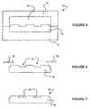
- Figure 5illustrates a mold tool 19 , having a first part 16 and a second part 17 , into which the substrate mold insert 10 fits.
- the mold tooltogether with the substrate mold insert, forms a space that will define the shape of the substrate 18 .
- a materialis injection molded into the space, to form the substrate 18 , as illustrated in Figure 5.
- the substratewill have a pattern corresponding to the negative image of the substrate mold insert.
- the substrate 18comprises a polymeric material, and may also include reinforcing materials, such as glass fibers.
- the substratecomprises a thermoplastic polymeric material, for example acrylonitrile butadiene styrene (ABS), acetal, acrylic, polycarbonate (PC), polyester, polyethylene, fluroplastic, polyimide, nylon, polyphenylene oxide, polypropylene (PP), polystyrene, polysulphone, polyvinyl chloride, poly(methacrylate), poly(methyl methacrylate), or mixture or copolymers thereof.
- the substrateincludes a polycarbonate, such as those used in making compact discs.
- the substratedoes not contain any reinforcing material, and only contains a thermoplastic polymeric material, such as a polycarbonate.
- the material injection molded into the space, to form the substrateis either the material of the substrate, such as a thermoplastic polymeric material, or components which will react to form the material of the substrate, such as monomers or polymeric precursors.
- a metallic layer 22is then formed on the substrate 18 .
- the metallic layermay be formed by, for example, evaporation or by sputtering.
- a mask 20may be used to prevent formation of the metallic layer on portions of the substrate that do not have a pattern.
- the metal layermay have almost any thickness, but preferably has a thickness at least as large as the depth of the channels of the pattern in the substrate.
- Figure 7illustrates a set of metallic deposits 28 .
- the set of metallic depositscorresponds to the pattern of the substrate 18 , and includes metallic deposits 26 in the substrate.
- the pattern 18is an electrode pattern
- the set of metallic depositsis an electrode set, and the metallic deposits form one or more electrodes.
- the set of metallic depositsis formed by removing those parts of the metallic layer 22 outside of the channels of the pattern shown in Figure 6, causing portions of the substrate surface outside the pattern to be exposed.
- the excess metallic layermay be remove by, for example, milling or chemical/mechanical polishing.
- the metallic depositshave a thickness which is the same as the depth of the channels of the pattern in the substrate, so that the set of metallic deposits and substrate surface together form a flat surface.
- FIG 8illustrates a lid mold insert 30 .
- the lid mold insertmay be made of any of the materials from which the substrate mold insert is made.
- the lid mold insertmay be formed by precision milling, lithography or laser ablation.
- Figure 9illustrates a mold tool 19 , having a first part 16 and a second part 17 , into which the lid mold insert 30 fits.
- the mold tooltogether with the lid mold insert, forms a space that will define the shape of the lid 32 .
- a materialis injection molded into the space, to form the lid 32 , as illustrated in Figure 9.
- the choice of materials of which the lid is made, as well as what materials are injection molded into the space to for the lid,are the same as those of the substrate.
- the lid and the substratemay be made of the same or different materials.
- the inside surface 34 of the lid 32is may be hydrophilisized, as illustrated in Figure 10. This causes an aqueous solution to wet the inside surface 34 . Hydrophilisation may be carried out by, for example, application of a surfactant, or treatment with a plasma formed from a gas containing oxygen. This plasma can also be used to clean the electrode surfaces. Also illustrated in Figure 10 are optional energy directors 24 and 24 , which are a part of the lid 32 .
- Figure 11illustrates aligning the lid 32 with the set of metallic deposits 28 .
- the inside surfacehere hydrophilisized
- the lid 32 and the set of metallic deposits 28are bonded together, and when the set of metallic deposits is an electrode set, they form a sensor 36 , as illustrated in Figure 12.
- a capillary channel 38forms between the inside surface of the lid 32 and a portion of the electrode set 28 .
- This capillary channelcan draw a fluid sample from its opening onto the metallic deposits of the electrode set.
- the lidmay be bonded to the electrode set a variety of was, including ultrasonic welding, or using an adhesive or a solvent.
- ultrasonic weldingcauses the material that forms the energy directors to bond the electrode set and the lid.
- the solventwill dissolve a portion of the material of the lid, the substrate, or both, causing them to adhere as the solvent evaporates.
- a groove or channelis included for solvent or adhesive bonding.
- Figure 14illustrates an embodiment of an electrode set 28 .
- the electrode setincludes two electrodes 44 and 44 .
- the electrodeshave contact pads 49 and 49 , that are electrically connected to the sensing region 110 of the electrode.
- lid 32that covers the electrodes, and includes a vent 52 , and the lid together with the substrate define a capillary channel 38 .
- the ventallows air to escape when the sample is applied to the opening of the capillary channel and flows towards the sensing region.
- the lidhas an opening through its top, and this opening is aligned over a portion of the metallic deposits, and a fluid sample may be placed through this opening directly onto the metallic deposits.
- Figure 13shows an electrode set 28 , including two electrodes 44 and 44 .
- the electrodeshave contact pads 49 and 49 , that are electrically connected to the sensing region 110 of the electrode.
- lid 32that covers the first and second electrodes, exposing only the sensing region and the contact pads; the lid together with the substrate also define a vent 52 , which allows air to escape when the sample is applied to the sensing region.
- a sensormay be used alone as a sensor strip for use in an electrochemical sensor.
- the sensormay be attached to a base, with the lid facing away from the base.
- the sensormay be attached to the base with an adhesive, such as an adhesive foil.
- a reagentmay be placed onto the sensor region of the electrode set.
- Figure 15illustrates three views of an electrode set 28 , showing the details of an electrode pattern. Shown in the figure are two electrodes 44 and 44 , each having a contact pad 49 and 49 and a sensing region 110 in electrical contact. Those portions of the pattern that do not have an electrode (and therefore the surface of the substrate in that portion did not have a channel) are designated as island (or islands) 50 . Although these regions are referred to as an island (or islands), they need not be completely surrounded by channels in the substrate.
- Each electrode 44is formed from a metallic channel.
- the distances shown in the figureare in millimeters.
- the electrodes (and therefore also the metallic deposits)are illustrated as having a width of 0.050 mm (50 ⁇ m).
- the widthmay be 1 ⁇ m to 1 mm, more preferably 5 ⁇ m to 300 ⁇ m, most preferably 10 ⁇ m to 100 ⁇ m.
- the widthmay vary in any given electrode set. The smallest width in a pattern corresponds to the feature size, since it is the smallest intentional feature in the pattern.
- the electrodesform interlacing fingers, in a rectilinear pattern.
- the values for the dimensions illustrated in Figure 14are for a single specific embodiment, and these values may be selected as need for the specific use.
- the length of the electrode setmay be 1.5 to 250 mm
- the widthmay be 0.4 to 40 mm
- the gap between the contact padsmaybe 1 ⁇ m to 5 mm
- the width of each contact padmay be 0.1 to 20 mm.
- the electrode pattern shown in Figure 14is symmetric; however this is not required, and irregular or asymmetric patters (or electrode shapes) are possible.
- the metallic channel and metallic layermay contain pure metals or alloys, or other materials which are metallic conductors.
- Examplesinclude aluminum, carbon (such as graphite), cobalt, copper, gallium, gold, indium, iridium, iron, lead, magnesium, mercury (as an amalgam), nickel, niobium, osmium, palladium, platinum, rhenium, rhodium, selenium, silicon (such as highly doped polycrystalline silicon), silver, tantalum, tin, titanium, tungsten, uranium, vanadium, zinc, zirconium, mixtures thereof, and alloys or metallic compounds of these elements.
- the metallic layerincludes gold, platinum, palladium, iridium, or alloys of these metals, since such noble metals and their alloys are unreactive in biological systems.
- the metallic layermay be any thickness, but preferably is 10 nm to 1 mm, more preferably, 20 nm to 100 ⁇ m, or even 25 nm to 1 ⁇ m.
- the depth of the pattern formed in substrateis preferably 10 nm to 1 mm, more preferably, 20 nm to 100 ⁇ m, or even 25 nm to 1 ⁇ m.
- the metallic layeris at least as thick as the pattern of channels formed in the substrate is deep; however, it is possible for the metal layer to be thicker or thinner than the channels are deep.
- the metallic depositswill have a maximum depth corresponding to the thickness of the metal layer, but through etching or milling, the depth of the metallic deposits may be less deep than the metallic layer is thick.
- the metallic layer, and/or the metal channelsmay be coated or plated with additional metal layers.
- the metallic layermay be copper; subsequently, the copper may be plated with a titanium/tungsten layer, and then a gold layer, and then milled, to form the desired electrodes.
- the coppermay be plated with a titanium/tungsten layer, and then a gold layer, and then milled, to form the desired electrodes.
- a single layer of goldis used, which is directly in contact with the substrate, since it allows for the entire elimination of wet chemical steps for the formation of the electrode sets.
- the metallic deposits and therefore the electrodes of the electrodes setsare set into the substrate; in screen printing all structures rest on top of the surface of the substrate.
- the metallic depositsare completely within groves in the surface of the substrate, i.e. the metallic deposits are inlaid within the surface of the substrate.
- metalis coated or plated onto the metallic deposits, they may extend out above the plane of the surface of the substrate.
- the baseis a supporting structure, and is preferably made of flexible polymer material, with a thickness sufficient to provide support to the sensor strip, for example polyester with a thickness of 6 mils.
- the adhesive foilis also a flexible polymer having a surfaces covered with an adhesive; these materials are also well known to those of ordinary skill in the art.
- the reagentis optional, and may be used to provide electrochemical probes for specific analytes.
- the starting reagentsare the reactants or components of the reagent, and are often compounded together in liquid form before application to the sensor region. The liquid may then evaporate, leaving the reagent in solid form.
- the choice of specific reagentdepends on the specific analyte or analytes to be measure, and are well known to those of ordinary skill in the art.
- a reagent for measurement of glucose in a human blood samplecontains 62.2 mg polyethylene oxide (mean molecular weight of 100-900 kilodaltons), 3.3 mg NATROSOL 250 M, 41.5 mg AVICEL RC-591 F, 89.4 mg monobasic potassium phosphate, 157.9 mg dibasic potassium phosphate, 437.3 mg potassium ferricyanide, 46.0 mg sodium succinate, 148.0 mg trehalose, 2.6 mg TRITON X-100 surfactant, and 2,000 to 9,000 units of enzyme activity per gram of reagent.
- the enzymeis prepared as an enzyme solution from 12.5 mg coenzyme PQQ and 1.21 million units of the apoenzyme of quinoprotein glucose dehydrogenase, forming a solution of quinoprotein glucose dehydrogenase.
- This reagentis described in WO 99/30152, pages 7-10.
- the processes and products describedinclude disposable biosensors, especially for use in diagnostic devices.
- electrochemical sensorsfor non-diagnostic uses, such as for measuring an analyte in any biological, environmental, or other, sample.
- any substrate containing metallic depositspreferably of a noble metal (gold, platinum, palladium, iridium, alloys thereof) in direct contact with an insulating substrate, such as a polymer.
- Such laminatescan have a variety of electrical function, including use as electrodes, electrical wires or connectors, microwave reflectors, etc.
- these substrates containing metallic depositshave a feature size of 100 ⁇ m or less, more preferably 1 to 100 ⁇ m, even more preferably 75 ⁇ m or less, including 5 to 50 ⁇ m, or even 5 to 20 ⁇ m.
Landscapes
- Chemical & Material Sciences (AREA)
- Life Sciences & Earth Sciences (AREA)
- Health & Medical Sciences (AREA)
- Biochemistry (AREA)
- General Physics & Mathematics (AREA)
- Electrochemistry (AREA)
- Physics & Mathematics (AREA)
- Analytical Chemistry (AREA)
- Molecular Biology (AREA)
- General Health & Medical Sciences (AREA)
- Chemical Kinetics & Catalysis (AREA)
- Immunology (AREA)
- Pathology (AREA)
- Apparatus Associated With Microorganisms And Enzymes (AREA)
- Injection Moulding Of Plastics Or The Like (AREA)
- Manufacturing Of Printed Circuit Boards (AREA)
- Manufacturing Of Printed Wiring (AREA)
- Moulds For Moulding Plastics Or The Like (AREA)
Abstract
Description
Claims (29)
- A method of making a set of metallic deposits, comprising:injection molding a substrate, wherein a pattern of channels is created in a surface ofsaid substrate, and said pattern of channels comprises at least one channel and at leastone island;forming a metallic layer on said surface, to form metallic deposits in said pattern; andremoving a portion of said metallic layer, to expose at least a portion of said at least oneisland.
- The method of Claim 1, wherein said set of metallic deposits is an electrode set, and saidpattern is an electrode pattern.
- The method of Claim 1 or 2, wherein said metallic layer comprises at least one metalselected from the group consisting of gold, platinum, palladium and iridium.
- The method of Claim 1, 2 or 3, wherein said substrate comprises a thermoplasticpolymer.
- The method of Claim 4, wherein said thermoplastic polymer is a polycarbonate.
- The method of Claim 2, wherein said metallic deposits have a width of 1 to 100 µm.
- A method of making a sensor, comprising:forming an electrode set by the method of Claim 2 or 4,andbonding a lid to said electrode set.
- The set of metallic deposits produced by the method of Claim 1.
- The electrode set produced by the method of Claim 2 or 4.
- The sensor produced by the method of Claim 7.
- A set of metallic deposits, comprising:a pattern of channels in a surface of a substrate, andmetallic deposits in said pattern,
wherein portions of said surface are exposed, andsaid substrate comprises a polymer. - The set of metallic deposits of Claim 11, wherein said polymer is a thermoplasticpolymer.
- The set of metallic deposits of Claim 12, wherein said polymer is a polycarbonate.
- The set of metallic deposits of Claim 11 or 13, wherein said metallic deposits comprise atleast one metal selected from the group consisting of gold, platinum, palladium andiridium.
- An electrode set, comprising:an electrode pattern in a surface of a substrate, andmetallic deposits in said pattern,
wherein said substrate comprises a polymer. - The electrode set of Claim 15, wherein said polymer is a thermoplastic polymer.
- The electrode set of Claim 16, wherein said polymer is a polycarbonate.
- A mold insert, comprising a metal,
wherein a reverse electrode pattern is in a surface of said mold insert. - A set of metallic deposits, comprising:a pattern of channels in a surface of a substrate, andmetallic deposits in said pattern,
wherein portions of said surface are exposed, andsaid pattern of channels are formed by injection molding. - The set of metallic deposits of Claim 19, wherein said substrate comprises athermoplastic polymer.
- The set of metallic deposits of Claim 20, wherein said substrate comprises apolycarbonate.
- The set of metallic deposits of Claim 19 or 21, wherein said metallic deposits comprise atleast one metal selected from the group consisting of gold, platinum, palladium andiridium.
- An electrode set, comprising:an electrode pattern in a surface of a substrate, andmetallic deposits in said pattern,
wherein said electrode pattern is formed by injection molding. - The electrode set of Claim 15 or 23, wherein portions of said surface are exposed.
- The electrode set of Claim 23, wherein said substrate comprises a thermoplasticpolymer.
- The electrode set of Claim 25, wherein said substrate comprises a polycarbonate.
- The electrode set of Claim 15, 17, 23 or 26, wherein said metallic deposits comprise atleast one metal selected from the group consisting of gold, platinum, palladium andiridium.
- The electrode set of Claim 15 or 23, wherein said metallic deposits have a width of 1 to100 µm.
- A sensor, comprising:the electrode set of Claim 15, 23 or 27, anda lid, on said electrode set.
Applications Claiming Priority (2)
| Application Number | Priority Date | Filing Date | Title |
|---|---|---|---|
| US09/433,629US20020139668A1 (en) | 1999-11-03 | 1999-11-03 | Embedded metallic deposits |
| US433629 | 1999-11-03 |
Publications (2)
| Publication Number | Publication Date |
|---|---|
| EP1098000A2true EP1098000A2 (en) | 2001-05-09 |
| EP1098000A3 EP1098000A3 (en) | 2003-10-08 |
Family
ID=23720902
Family Applications (1)
| Application Number | Title | Priority Date | Filing Date |
|---|---|---|---|
| EP00123693AWithdrawnEP1098000A3 (en) | 1999-11-03 | 2000-10-31 | Embedded metallic deposits forming an electrode set for an electrochemical sensor strip |
Country Status (5)
| Country | Link |
|---|---|
| US (2) | US20020139668A1 (en) |
| EP (1) | EP1098000A3 (en) |
| JP (1) | JP2001189546A (en) |
| AU (1) | AU778920B2 (en) |
| CA (1) | CA2324827A1 (en) |
Cited By (16)
| Publication number | Priority date | Publication date | Assignee | Title |
|---|---|---|---|---|
| EP1195441A1 (en)* | 2000-10-06 | 2002-04-10 | Roche Diagnostics GmbH | Biosensor |
| EP1203823A1 (en)* | 2000-11-01 | 2002-05-08 | Roche Diagnostics GmbH | Biosensor |
| WO2002077606A3 (en)* | 2001-03-23 | 2003-02-06 | Virotek Llc | Electrochemical sensor and method thereof |
| US6576102B1 (en) | 2001-03-23 | 2003-06-10 | Virotek, L.L.C. | Electrochemical sensor and method thereof |
| EP1203956A3 (en)* | 2000-11-01 | 2003-10-22 | Roche Diagnostics GmbH | Biosensor with flow channel |
| EP1302545A3 (en)* | 2001-10-09 | 2003-11-05 | Roche Diagnostics GmbH | Enzyme Biosensor |
| WO2005005974A1 (en) | 2003-06-17 | 2005-01-20 | Huang, Alice, Y. | Structure and manufacturing method of disposable electrochemical sensor strip |
| WO2005066616A3 (en)* | 2003-06-20 | 2005-11-10 | Roche Diagnostics Gmbh | Biosensor and method of making |
| WO2008012351A1 (en)* | 2006-07-28 | 2008-01-31 | Iee International Electronics & Engineering S.A. | Method of producing a film-type sensor |
| WO2007114943A3 (en)* | 2006-04-04 | 2008-03-06 | Medtronic Minimed Inc | Methods and materials for controlling the electrochemistry of analyte sensors |
| CN100432660C (en)* | 2003-05-07 | 2008-11-12 | 黄椿木 | Structure of electrochemical sensing test block and producing method thereof |
| US7740746B2 (en) | 2003-06-17 | 2010-06-22 | Delta Electronics, Inc. | Disposable electrochemical sensor strip |
| EP1592965A4 (en)* | 2003-01-31 | 2010-07-14 | Huang Chun Mu | Method for manufacturing electrochemical sensor and structure thereof |
| US7892849B2 (en) | 2003-06-20 | 2011-02-22 | Roche Diagnostics Operations, Inc. | Reagent stripe for test strip |
| US8287703B2 (en) | 1999-10-04 | 2012-10-16 | Roche Diagnostics Operations, Inc. | Biosensor and method of making |
| EP3147657A4 (en)* | 2014-05-20 | 2017-11-01 | Kuang Hong Precision Co., Ltd. | Electrochemical sensitive test piece and manufacturing method therefor |
Families Citing this family (7)
| Publication number | Priority date | Publication date | Assignee | Title |
|---|---|---|---|---|
| US8652235B2 (en)* | 2004-08-30 | 2014-02-18 | Energy & Environmental Research Center Foundation | Sorbents for the oxidation and removal of mercury |
| US10343114B2 (en)* | 2004-08-30 | 2019-07-09 | Midwest Energy Emissions Corp | Sorbents for the oxidation and removal of mercury |
| US20060160249A1 (en)* | 2005-01-17 | 2006-07-20 | Tien-Yu Chou | Method for fabricating biochips or biosensors using cd/dvd making compatible processes |
| WO2007046335A1 (en)* | 2005-10-17 | 2007-04-26 | Sumitomo Electric Industries, Ltd. | Sensor chip and method for producing the same |
| EP2172152A1 (en)* | 2008-10-06 | 2010-04-07 | Nederlandse Organisatie voor toegepast-natuurwetenschappelijk Onderzoek TNO | Electrode for medical applications. |
| US10577264B2 (en)* | 2012-11-21 | 2020-03-03 | The Hong Kong University Of Science And Technology | Pulsed electric field for drinking water disinfection |
| US10359010B2 (en)* | 2014-02-16 | 2019-07-23 | K&N Engineering, Inc. | Air box with integrated filter media |
Family Cites Families (35)
| Publication number | Priority date | Publication date | Assignee | Title |
|---|---|---|---|---|
| US3438127A (en)* | 1965-10-21 | 1969-04-15 | Friden Inc | Manufacture of circuit modules using etched molds |
| US4059479A (en)* | 1973-08-10 | 1977-11-22 | Hisaji Tanazawa | Method of forming an embossed pattern |
| US3990142A (en)* | 1973-10-02 | 1976-11-09 | Jerobee Industries, Inc. | Circuit board, method of making the circuit board and improved die for making said board |
| SE404863B (en)* | 1975-12-17 | 1978-10-30 | Perstorp Ab | PROCEDURE FOR MAKING A MULTIPLE STORE CARD |
| US4223321A (en)* | 1979-04-30 | 1980-09-16 | The Mead Corporation | Planar-faced electrode for ink jet printer and method of manufacture |
| JPS5797970U (en)* | 1980-12-08 | 1982-06-16 | ||
| US4402998A (en)* | 1982-01-04 | 1983-09-06 | Western Electric Co., Inc. | Method for providing an adherent electroless metal coating on an epoxy surface |
| US4532152A (en)* | 1982-03-05 | 1985-07-30 | Elarde Vito D | Fabrication of a printed circuit board with metal-filled channels |
| US4517739A (en)* | 1983-11-21 | 1985-05-21 | Northern Telecom Limited | Method for making circuit boards with die stamped contact pads and conductive ink circuit patterns |
| US5141868A (en)* | 1984-06-13 | 1992-08-25 | Internationale Octrooi Maatschappij "Octropa" Bv | Device for use in chemical test procedures |
| US4651417A (en)* | 1984-10-23 | 1987-03-24 | New West Technology Corporation | Method for forming printed circuit board |
| US4812421A (en)* | 1987-10-26 | 1989-03-14 | Motorola, Inc. | Tab-type semiconductor process |
| IL75160A0 (en)* | 1985-05-10 | 1985-09-29 | Yitzhaq Lipsker | Soil drilling equipment |
| US4816427A (en)* | 1986-09-02 | 1989-03-28 | Dennis Richard K | Process for connecting lead frame to semiconductor device |
| US4969257A (en)* | 1987-09-04 | 1990-11-13 | Shinko Electric Industries, Co., Ltd. | Transfer sheet and process for making a circuit substrate |
| US4827611A (en)* | 1988-03-28 | 1989-05-09 | Control Data Corporation | Compliant S-leads for chip carriers |
| US4831723A (en)* | 1988-04-12 | 1989-05-23 | Kaufman Lance R | Direct bond circuit assembly with crimped lead frame |
| GB8913450D0 (en)* | 1989-06-12 | 1989-08-02 | Philips Electronic Associated | Electrical device manufacture,particularly infrared detector arrays |
| DE4010669C1 (en)* | 1990-04-03 | 1991-04-11 | Kernforschungszentrum Karlsruhe Gmbh, 7500 Karlsruhe, De | |
| US5030144A (en)* | 1990-04-13 | 1991-07-09 | North American Specialties Corporation | Solder-bearing lead |
| JPH0476985A (en)* | 1990-07-18 | 1992-03-11 | Cmk Corp | Manufacturing method for printed wiring boards |
| JP2747096B2 (en)* | 1990-07-24 | 1998-05-06 | 北川工業株式会社 | Method for manufacturing three-dimensional circuit board |
| US5097101A (en)* | 1991-02-05 | 1992-03-17 | Tektronix, Inc. | Method of forming a conductive contact bump on a flexible substrate and a flexible substrate |
| DE59108784D1 (en)* | 1991-04-01 | 1997-08-21 | Akcionernoe Obscestvo Otkrytog | MULTIPLE LAYER BOARD AND METHOD FOR THEIR PRODUCTION |
| US5351393A (en)* | 1991-05-28 | 1994-10-04 | Dimensonal Circuits Corporation | Method of mounting a surface-mountable IC to a converter board |
| EP0545328B1 (en)* | 1991-11-29 | 1997-03-19 | Hitachi Chemical Co., Ltd. | Printed circuit board manufacturing process |
| US5390412A (en)* | 1993-04-08 | 1995-02-21 | Gregoire; George D. | Method for making printed circuit boards |
| US5373111A (en)* | 1993-11-19 | 1994-12-13 | Delco Electronics Corporation | Bond pad having a patterned bonding surface |
| US5391250A (en)* | 1994-03-15 | 1995-02-21 | Minimed Inc. | Method of fabricating thin film sensors |
| DE4438053C2 (en)* | 1994-10-25 | 2002-05-02 | Harting Elektrooptische Bauteile Gmbh & Co Kg | Method for producing an electrically conductive structure |
| US5885470A (en)* | 1997-04-14 | 1999-03-23 | Caliper Technologies Corporation | Controlled fluid transport in microfabricated polymeric substrates |
| AU6157898A (en)* | 1997-02-06 | 1998-08-26 | E. Heller & Company | Small volume (in vitro) analyte sensor |
| US5798031A (en)* | 1997-05-12 | 1998-08-25 | Bayer Corporation | Electrochemical biosensor |
| US6134461A (en)* | 1998-03-04 | 2000-10-17 | E. Heller & Company | Electrochemical analyte |
| US6150119A (en)* | 1999-01-19 | 2000-11-21 | Caliper Technologies Corp. | Optimized high-throughput analytical system |
- 1999
- 1999-11-03USUS09/433,629patent/US20020139668A1/ennot_activeAbandoned
- 2000
- 2000-10-31EPEP00123693Apatent/EP1098000A3/ennot_activeWithdrawn
- 2000-11-01CACA002324827Apatent/CA2324827A1/ennot_activeAbandoned
- 2000-11-02AUAU69695/00Apatent/AU778920B2/ennot_activeCeased
- 2000-11-02JPJP2000336574Apatent/JP2001189546A/enactivePending
- 2002
- 2002-12-02USUS10/307,635patent/US20040000371A1/ennot_activeAbandoned
Cited By (27)
| Publication number | Priority date | Publication date | Assignee | Title |
|---|---|---|---|---|
| US8287703B2 (en) | 1999-10-04 | 2012-10-16 | Roche Diagnostics Operations, Inc. | Biosensor and method of making |
| US8551308B2 (en) | 1999-10-04 | 2013-10-08 | Roche Diagnostics Operations, Inc. | Biosensor and method of making |
| EP1195441A1 (en)* | 2000-10-06 | 2002-04-10 | Roche Diagnostics GmbH | Biosensor |
| US7287318B2 (en) | 2000-10-06 | 2007-10-30 | Roche Diagnostics Operations, Inc. | Biosensor |
| US6645359B1 (en) | 2000-10-06 | 2003-11-11 | Roche Diagnostics Corporation | Biosensor |
| US6814843B1 (en) | 2000-11-01 | 2004-11-09 | Roche Diagnostics Corporation | Biosensor |
| EP1203956A3 (en)* | 2000-11-01 | 2003-10-22 | Roche Diagnostics GmbH | Biosensor with flow channel |
| EP1203823A1 (en)* | 2000-11-01 | 2002-05-08 | Roche Diagnostics GmbH | Biosensor |
| US6911621B2 (en) | 2000-11-01 | 2005-06-28 | Roche Diagnostics Corporation | Biosensor |
| US6576102B1 (en) | 2001-03-23 | 2003-06-10 | Virotek, L.L.C. | Electrochemical sensor and method thereof |
| US6572745B2 (en)* | 2001-03-23 | 2003-06-03 | Virotek, L.L.C. | Electrochemical sensor and method thereof |
| WO2002077606A3 (en)* | 2001-03-23 | 2003-02-06 | Virotek Llc | Electrochemical sensor and method thereof |
| US6849216B2 (en) | 2001-03-23 | 2005-02-01 | Virotek, L.L.C. | Method of making sensor |
| EP1302545A3 (en)* | 2001-10-09 | 2003-11-05 | Roche Diagnostics GmbH | Enzyme Biosensor |
| US6755949B1 (en) | 2001-10-09 | 2004-06-29 | Roche Diagnostics Corporation | Biosensor |
| US9541519B2 (en) | 2002-10-18 | 2017-01-10 | Medtronic Minimed, Inc. | Amperometric sensor electrodes |
| EP1592965A4 (en)* | 2003-01-31 | 2010-07-14 | Huang Chun Mu | Method for manufacturing electrochemical sensor and structure thereof |
| CN100432660C (en)* | 2003-05-07 | 2008-11-12 | 黄椿木 | Structure of electrochemical sensing test block and producing method thereof |
| WO2005005974A1 (en) | 2003-06-17 | 2005-01-20 | Huang, Alice, Y. | Structure and manufacturing method of disposable electrochemical sensor strip |
| US7740746B2 (en) | 2003-06-17 | 2010-06-22 | Delta Electronics, Inc. | Disposable electrochemical sensor strip |
| US8187446B2 (en) | 2003-06-17 | 2012-05-29 | Chun-Mu Huang | Method of manufacturing a disposable electrochemical sensor strip |
| US7063776B2 (en) | 2003-06-17 | 2006-06-20 | Chun-Mu Huang | Structure and manufacturing method of disposable electrochemical sensor strip |
| US7892849B2 (en) | 2003-06-20 | 2011-02-22 | Roche Diagnostics Operations, Inc. | Reagent stripe for test strip |
| WO2005066616A3 (en)* | 2003-06-20 | 2005-11-10 | Roche Diagnostics Gmbh | Biosensor and method of making |
| WO2007114943A3 (en)* | 2006-04-04 | 2008-03-06 | Medtronic Minimed Inc | Methods and materials for controlling the electrochemistry of analyte sensors |
| WO2008012351A1 (en)* | 2006-07-28 | 2008-01-31 | Iee International Electronics & Engineering S.A. | Method of producing a film-type sensor |
| EP3147657A4 (en)* | 2014-05-20 | 2017-11-01 | Kuang Hong Precision Co., Ltd. | Electrochemical sensitive test piece and manufacturing method therefor |
Also Published As
| Publication number | Publication date |
|---|---|
| AU6969500A (en) | 2001-05-10 |
| JP2001189546A (en) | 2001-07-10 |
| EP1098000A3 (en) | 2003-10-08 |
| US20040000371A1 (en) | 2004-01-01 |
| AU778920B2 (en) | 2004-12-23 |
| CA2324827A1 (en) | 2001-05-03 |
| US20020139668A1 (en) | 2002-10-03 |
Similar Documents
| Publication | Publication Date | Title |
|---|---|---|
| AU778920B2 (en) | Embedded metallic deposits | |
| CN1180250C (en) | Electrochemical biosensor test strip, fabrication method thereof and electrochemical biosensor | |
| US8354012B2 (en) | Electrochemical cell | |
| CA2386172C (en) | Patterned laminates and electrodes with laser defined features | |
| US9222909B2 (en) | Biosensor and method for producing the same | |
| US20020121439A1 (en) | Electrochemical microsensor package | |
| US20070266871A1 (en) | Diagnostic test media and methods for the manufacture thereof | |
| CN1928541A (en) | Electrochemical cell | |
| WO2005047894A1 (en) | Circuit for electrochemical sensor strip | |
| TW200809188A (en) | Method of manufacturing a diagnostic test strip | |
| CA2499867A1 (en) | Method of making sensor electrodes | |
| EP2008087A2 (en) | Laminated biosensor and its manufacturing method | |
| JP2013190212A (en) | Biosensor and manufacturing method of the same | |
| JP2007298325A (en) | Electrode tip and manufacturing method thereof | |
| JP2006133219A (en) | Micro-fluid analytical system | |
| JP2006308458A (en) | Biosensor | |
| JP2006105987A (en) | Manufacturing method of analysis module having accessible electrically conductive contact pad for microfluidic analytical system | |
| EP1969135A2 (en) | Process of making electrodes for test sensors | |
| JPH05133930A (en) | Oxygen concentration sensor | |
| CN120227021A (en) | A sensor for analytes and a method for preparing the same | |
| HK1090978A (en) | Electrochemical cell | |
| HK1104603A (en) | Electrochemical cell | |
| HK1088030B (en) | Fusible conductive ink for use in manufacturing microfluidic analytical systems |
Legal Events
| Date | Code | Title | Description |
|---|---|---|---|
| PUAI | Public reference made under article 153(3) epc to a published international application that has entered the european phase | Free format text:ORIGINAL CODE: 0009012 | |
| 17P | Request for examination filed | Effective date:20001031 | |
| AK | Designated contracting states | Kind code of ref document:A2 Designated state(s):AT BE CH CY DE DK ES FI FR GB GR IE IT LI LU MC NL PT SE | |
| AX | Request for extension of the european patent | Free format text:AL;LT;LV;MK;RO;SI | |
| RIC1 | Information provided on ipc code assigned before grant | Ipc:7G 01N 33/543 B Ipc:7G 01N 33/487 B Ipc:7G 01N 27/28 B Ipc:7G 01N 27/403 B Ipc:7A 61B 5/00 B Ipc:7H 05K 3/04 B Ipc:7C 12Q 1/00 A | |
| PUAL | Search report despatched | Free format text:ORIGINAL CODE: 0009013 | |
| AK | Designated contracting states | Kind code of ref document:A3 Designated state(s):AT BE CH CY DE DK ES FI FR GB GR IE IT LI LU MC NL PT SE | |
| AX | Request for extension of the european patent | Extension state:AL LT LV MK RO SI | |
| AKX | Designation fees paid | Designated state(s):AT BE CH CY DE DK ES FI FR GB GR IE IT LI LU MC NL PT SE | |
| 17Q | First examination report despatched | Effective date:20050701 | |
| RAP1 | Party data changed (applicant data changed or rights of an application transferred) | Owner name:ROCHE DIAGNOSTICS OPERATIONS, INC. | |
| STAA | Information on the status of an ep patent application or granted ep patent | Free format text:STATUS: THE APPLICATION IS DEEMED TO BE WITHDRAWN | |
| 18D | Application deemed to be withdrawn | Effective date:20080501 |