EP1085319B1 - A device for detecting an analyte in a sample based on organic materials - Google Patents
A device for detecting an analyte in a sample based on organic materialsDownload PDFInfo
- Publication number
- EP1085319B1 EP1085319B1EP00870200AEP00870200AEP1085319B1EP 1085319 B1EP1085319 B1EP 1085319B1EP 00870200 AEP00870200 AEP 00870200AEP 00870200 AEP00870200 AEP 00870200AEP 1085319 B1EP1085319 B1EP 1085319B1
- Authority
- EP
- European Patent Office
- Prior art keywords
- layer
- recited
- analyte
- sample
- dielectric
- Prior art date
- Legal status (The legal status is an assumption and is not a legal conclusion. Google has not performed a legal analysis and makes no representation as to the accuracy of the status listed.)
- Expired - Lifetime
Links
- 239000012491analyteSubstances0.000titleclaimsdescription53
- 239000011368organic materialSubstances0.000titledescription4
- 239000000463materialSubstances0.000claimsdescription42
- 239000003989dielectric materialSubstances0.000claimsdescription20
- 239000012528membraneSubstances0.000claimsdescription19
- 239000004065semiconductorSubstances0.000claimsdescription16
- 230000005669field effectEffects0.000claimsdescription13
- -1poly(p-phenylene)Polymers0.000claimsdescription9
- 229920000642polymerPolymers0.000claimsdescription8
- 230000037361pathwayEffects0.000claimsdescription6
- GWEVSGVZZGPLCZ-UHFFFAOYSA-NTitan oxideChemical compoundO=[Ti]=OGWEVSGVZZGPLCZ-UHFFFAOYSA-N0.000claimsdescription4
- 239000011159matrix materialSubstances0.000claimsdescription4
- 229920000128polypyrrolePolymers0.000claimsdescription4
- 229920000265PolyparaphenylenePolymers0.000claimsdescription3
- 239000007769metal materialSubstances0.000claimsdescription3
- 229920000553poly(phenylenevinylene)Polymers0.000claimsdescription3
- 229920000123polythiophenePolymers0.000claimsdescription3
- QZVHYFUVMQIGGM-UHFFFAOYSA-N2-HexylthiopheneChemical compoundCCCCCCC1=CC=CS1QZVHYFUVMQIGGM-UHFFFAOYSA-N0.000claimsdescription2
- 229910015846BaxSr1-xTiO3Inorganic materials0.000claimsdescription2
- 229910012463LiTaO3Inorganic materials0.000claimsdescription2
- 229910003781PbTiO3Inorganic materials0.000claimsdescription2
- 229910002370SrTiO3Inorganic materials0.000claimsdescription2
- 229910002113barium titanateInorganic materials0.000claimsdescription2
- 229910021523barium zirconateInorganic materials0.000claimsdescription2
- 125000005678ethenylene groupChemical group[H]C([*:1])=C([H])[*:2]0.000claimsdescription2
- SLIUAWYAILUBJU-UHFFFAOYSA-NpentaceneChemical compoundC1=CC=CC2=CC3=CC4=CC5=CC=CC=C5C=C4C=C3C=C21SLIUAWYAILUBJU-UHFFFAOYSA-N0.000claimsdescription2
- 229920001296polysiloxanePolymers0.000claimsdescription2
- PBCFLUZVCVVTBY-UHFFFAOYSA-Ntantalum pentoxideInorganic materialsO=[Ta](=O)O[Ta](=O)=OPBCFLUZVCVVTBY-UHFFFAOYSA-N0.000claimsdescription2
- 150000002500ionsChemical class0.000description20
- 239000000126substanceSubstances0.000description17
- 238000001514detection methodMethods0.000description11
- 230000000694effectsEffects0.000description10
- XUIMIQQOPSSXEZ-UHFFFAOYSA-NSiliconChemical compound[Si]XUIMIQQOPSSXEZ-UHFFFAOYSA-N0.000description9
- 238000000151depositionMethods0.000description9
- 229910052710siliconInorganic materials0.000description9
- 239000010703siliconSubstances0.000description8
- 230000008859changeEffects0.000description7
- 230000003993interactionEffects0.000description7
- 238000004519manufacturing processMethods0.000description7
- 238000012544monitoring processMethods0.000description7
- 239000000243solutionSubstances0.000description7
- 230000008901benefitEffects0.000description6
- 230000008021depositionEffects0.000description6
- 239000007789gasSubstances0.000description6
- 238000000034methodMethods0.000description6
- 230000004044responseEffects0.000description6
- 102000004190EnzymesHuman genes0.000description5
- 108090000790EnzymesProteins0.000description5
- 239000003792electrolyteSubstances0.000description5
- 238000012545processingMethods0.000description5
- 239000007864aqueous solutionSubstances0.000description4
- HVYWMOMLDIMFJA-DPAQBDIFSA-NcholesterolChemical compoundC1C=C2C[C@@H](O)CC[C@]2(C)[C@@H]2[C@@H]1[C@@H]1CC[C@H]([C@H](C)CCCC(C)C)[C@@]1(C)CC2HVYWMOMLDIMFJA-DPAQBDIFSA-N0.000description4
- 229920000547conjugated polymerPolymers0.000description4
- 238000005516engineering processMethods0.000description4
- 229910052809inorganic oxideInorganic materials0.000description4
- 239000000203mixtureSubstances0.000description4
- 230000007935neutral effectEffects0.000description4
- 239000000758substrateSubstances0.000description4
- 229910052581Si3N4Inorganic materials0.000description3
- 239000011149active materialSubstances0.000description3
- 230000000984immunochemical effectEffects0.000description3
- 239000002184metalSubstances0.000description3
- 229910052751metalInorganic materials0.000description3
- 239000004033plasticSubstances0.000description3
- 229920003023plasticPolymers0.000description3
- 230000035945sensitivityEffects0.000description3
- HQVNEWCFYHHQES-UHFFFAOYSA-Nsilicon nitrideChemical compoundN12[Si]34N5[Si]62N3[Si]51N64HQVNEWCFYHHQES-UHFFFAOYSA-N0.000description3
- 239000007787solidSubstances0.000description3
- 238000004528spin coatingMethods0.000description3
- 239000010409thin filmSubstances0.000description3
- HEDRZPFGACZZDS-UHFFFAOYSA-NChloroformChemical compoundClC(Cl)ClHEDRZPFGACZZDS-UHFFFAOYSA-N0.000description2
- WQZGKKKJIJFFOK-GASJEMHNSA-NGlucoseNatural productsOC[C@H]1OC(O)[C@H](O)[C@@H](O)[C@@H]1OWQZGKKKJIJFFOK-GASJEMHNSA-N0.000description2
- VYPSYNLAJGMNEJ-UHFFFAOYSA-NSilicium dioxideChemical compoundO=[Si]=OVYPSYNLAJGMNEJ-UHFFFAOYSA-N0.000description2
- WQZGKKKJIJFFOK-VFUOTHLCSA-Nbeta-D-glucoseChemical compoundOC[C@H]1O[C@@H](O)[C@H](O)[C@@H](O)[C@@H]1OWQZGKKKJIJFFOK-VFUOTHLCSA-N0.000description2
- 239000008280bloodSubstances0.000description2
- 210000004369bloodAnatomy0.000description2
- 230000019522cellular metabolic processEffects0.000description2
- 239000013626chemical specieSubstances0.000description2
- 235000012000cholesterolNutrition0.000description2
- 238000003776cleavage reactionMethods0.000description2
- 230000005684electric fieldEffects0.000description2
- 238000004070electrodepositionMethods0.000description2
- 238000006911enzymatic reactionMethods0.000description2
- 238000005530etchingMethods0.000description2
- 230000008020evaporationEffects0.000description2
- 238000001704evaporationMethods0.000description2
- 239000010408filmSubstances0.000description2
- 239000008103glucoseSubstances0.000description2
- PCHJSUWPFVWCPO-UHFFFAOYSA-NgoldChemical compound[Au]PCHJSUWPFVWCPO-UHFFFAOYSA-N0.000description2
- 239000010931goldSubstances0.000description2
- 229910052737goldInorganic materials0.000description2
- 229940088597hormoneDrugs0.000description2
- 239000005556hormoneSubstances0.000description2
- 230000010354integrationEffects0.000description2
- 150000004767nitridesChemical class0.000description2
- BASFCYQUMIYNBI-UHFFFAOYSA-NplatinumChemical compound[Pt]BASFCYQUMIYNBI-UHFFFAOYSA-N0.000description2
- 229920000301poly(3-hexylthiophene-2,5-diyl) polymerPolymers0.000description2
- 229920006254polymer filmPolymers0.000description2
- 230000008569processEffects0.000description2
- 230000007017scissionEffects0.000description2
- 229910052814silicon oxideInorganic materials0.000description2
- 239000002210silicon-based materialSubstances0.000description2
- 230000002123temporal effectEffects0.000description2
- XLYOFNOQVPJJNP-UHFFFAOYSA-NwaterSubstancesOXLYOFNOQVPJJNP-UHFFFAOYSA-N0.000description2
- MIOPJNTWMNEORI-GMSGAONNSA-N(S)-camphorsulfonic acidChemical compoundC1C[C@@]2(CS(O)(=O)=O)C(=O)C[C@@H]1C2(C)CMIOPJNTWMNEORI-GMSGAONNSA-N0.000description1
- NLMDJJTUQPXZFG-UHFFFAOYSA-N1,4,10,13-tetraoxa-7,16-diazacyclooctadecaneChemical compoundC1COCCOCCNCCOCCOCCN1NLMDJJTUQPXZFG-UHFFFAOYSA-N0.000description1
- 239000004593EpoxySubstances0.000description1
- 239000004642PolyimideSubstances0.000description1
- 239000004743PolypropyleneSubstances0.000description1
- 241000206607Porphyra umbilicalisSpecies0.000description1
- 108010067973ValinomycinProteins0.000description1
- 238000010521absorption reactionMethods0.000description1
- 239000004411aluminiumSubstances0.000description1
- 229910052782aluminiumInorganic materials0.000description1
- XAGFODPZIPBFFR-UHFFFAOYSA-NaluminiumChemical compound[Al]XAGFODPZIPBFFR-UHFFFAOYSA-N0.000description1
- PNEYBMLMFCGWSK-UHFFFAOYSA-Naluminium oxideInorganic materials[O-2].[O-2].[O-2].[Al+3].[Al+3]PNEYBMLMFCGWSK-UHFFFAOYSA-N0.000description1
- 150000001450anionsChemical class0.000description1
- 239000000427antigenSubstances0.000description1
- 102000036639antigensHuman genes0.000description1
- 108091007433antigensProteins0.000description1
- 238000003491arrayMethods0.000description1
- MIOPJNTWMNEORI-UHFFFAOYSA-Ncamphorsulfonic acidChemical compoundC1CC2(CS(O)(=O)=O)C(=O)CC1C2(C)CMIOPJNTWMNEORI-UHFFFAOYSA-N0.000description1
- 238000012512characterization methodMethods0.000description1
- 125000003636chemical groupChemical group0.000description1
- 238000006243chemical reactionMethods0.000description1
- 238000010668complexation reactionMethods0.000description1
- FCFNRCROJUBPLU-UHFFFAOYSA-Ncompound M126Natural productsCC(C)C1NC(=O)C(C)OC(=O)C(C(C)C)NC(=O)C(C(C)C)OC(=O)C(C(C)C)NC(=O)C(C)OC(=O)C(C(C)C)NC(=O)C(C(C)C)OC(=O)C(C(C)C)NC(=O)C(C)OC(=O)C(C(C)C)NC(=O)C(C(C)C)OC1=OFCFNRCROJUBPLU-UHFFFAOYSA-N0.000description1
- 150000003983crown ethersChemical class0.000description1
- 239000002739cryptandSubstances0.000description1
- 238000005137deposition processMethods0.000description1
- 238000001312dry etchingMethods0.000description1
- 230000002255enzymatic effectEffects0.000description1
- 239000003822epoxy resinSubstances0.000description1
- 229910021397glassy carbonInorganic materials0.000description1
- 229920001903high density polyethylenePolymers0.000description1
- 239000004700high-density polyethyleneSubstances0.000description1
- 238000004770highest occupied molecular orbitalMethods0.000description1
- 125000002887hydroxy groupChemical group[H]O*0.000description1
- 229910010272inorganic materialInorganic materials0.000description1
- 239000011147inorganic materialSubstances0.000description1
- 238000005342ion exchangeMethods0.000description1
- 238000001459lithographyMethods0.000description1
- 238000004768lowest unoccupied molecular orbitalMethods0.000description1
- 238000000691measurement methodMethods0.000description1
- 230000007246mechanismEffects0.000description1
- 230000002503metabolic effectEffects0.000description1
- 150000002894organic compoundsChemical class0.000description1
- 229920000620organic polymerPolymers0.000description1
- 229910052697platinumInorganic materials0.000description1
- 229920000052poly(p-xylylene)Polymers0.000description1
- 229920000767polyanilinePolymers0.000description1
- 229920000647polyepoxidePolymers0.000description1
- 229920001721polyimidePolymers0.000description1
- 229920001155polypropylenePolymers0.000description1
- 229920001343polytetrafluoroethylenePolymers0.000description1
- 238000001552radio frequency sputter depositionMethods0.000description1
- 238000011160researchMethods0.000description1
- 241000894007speciesSpecies0.000description1
- 238000002207thermal evaporationMethods0.000description1
- FCFNRCROJUBPLU-DNDCDFAISA-NvalinomycinChemical compoundCC(C)[C@@H]1NC(=O)[C@H](C)OC(=O)[C@@H](C(C)C)NC(=O)[C@@H](C(C)C)OC(=O)[C@H](C(C)C)NC(=O)[C@H](C)OC(=O)[C@@H](C(C)C)NC(=O)[C@@H](C(C)C)OC(=O)[C@H](C(C)C)NC(=O)[C@H](C)OC(=O)[C@@H](C(C)C)NC(=O)[C@@H](C(C)C)OC1=OFCFNRCROJUBPLU-DNDCDFAISA-N0.000description1
Images


Classifications
- G—PHYSICS
- G01—MEASURING; TESTING
- G01N—INVESTIGATING OR ANALYSING MATERIALS BY DETERMINING THEIR CHEMICAL OR PHYSICAL PROPERTIES
- G01N27/00—Investigating or analysing materials by the use of electric, electrochemical, or magnetic means
- G01N27/26—Investigating or analysing materials by the use of electric, electrochemical, or magnetic means by investigating electrochemical variables; by using electrolysis or electrophoresis
- G01N27/403—Cells and electrode assemblies
- G01N27/414—Ion-sensitive or chemical field-effect transistors, i.e. ISFETS or CHEMFETS
- H—ELECTRICITY
- H01—ELECTRIC ELEMENTS
- H01L—SEMICONDUCTOR DEVICES NOT COVERED BY CLASS H10
- H01L21/00—Processes or apparatus adapted for the manufacture or treatment of semiconductor or solid state devices or of parts thereof
- H01L21/02—Manufacture or treatment of semiconductor devices or of parts thereof
- H01L21/02104—Forming layers
- H01L21/02107—Forming insulating materials on a substrate
- H01L21/02109—Forming insulating materials on a substrate characterised by the type of layer, e.g. type of material, porous/non-porous, pre-cursors, mixtures or laminates
- H01L21/02112—Forming insulating materials on a substrate characterised by the type of layer, e.g. type of material, porous/non-porous, pre-cursors, mixtures or laminates characterised by the material of the layer
- H01L21/02172—Forming insulating materials on a substrate characterised by the type of layer, e.g. type of material, porous/non-porous, pre-cursors, mixtures or laminates characterised by the material of the layer the material containing at least one metal element, e.g. metal oxides, metal nitrides, metal oxynitrides or metal carbides
- H01L21/02175—Forming insulating materials on a substrate characterised by the type of layer, e.g. type of material, porous/non-porous, pre-cursors, mixtures or laminates characterised by the material of the layer the material containing at least one metal element, e.g. metal oxides, metal nitrides, metal oxynitrides or metal carbides characterised by the metal
- H01L21/02183—Forming insulating materials on a substrate characterised by the type of layer, e.g. type of material, porous/non-porous, pre-cursors, mixtures or laminates characterised by the material of the layer the material containing at least one metal element, e.g. metal oxides, metal nitrides, metal oxynitrides or metal carbides characterised by the metal the material containing tantalum, e.g. Ta2O5
- H—ELECTRICITY
- H01—ELECTRIC ELEMENTS
- H01L—SEMICONDUCTOR DEVICES NOT COVERED BY CLASS H10
- H01L21/00—Processes or apparatus adapted for the manufacture or treatment of semiconductor or solid state devices or of parts thereof
- H01L21/02—Manufacture or treatment of semiconductor devices or of parts thereof
- H01L21/02104—Forming layers
- H01L21/02107—Forming insulating materials on a substrate
- H01L21/02109—Forming insulating materials on a substrate characterised by the type of layer, e.g. type of material, porous/non-porous, pre-cursors, mixtures or laminates
- H01L21/02112—Forming insulating materials on a substrate characterised by the type of layer, e.g. type of material, porous/non-porous, pre-cursors, mixtures or laminates characterised by the material of the layer
- H01L21/02172—Forming insulating materials on a substrate characterised by the type of layer, e.g. type of material, porous/non-porous, pre-cursors, mixtures or laminates characterised by the material of the layer the material containing at least one metal element, e.g. metal oxides, metal nitrides, metal oxynitrides or metal carbides
- H01L21/02175—Forming insulating materials on a substrate characterised by the type of layer, e.g. type of material, porous/non-porous, pre-cursors, mixtures or laminates characterised by the material of the layer the material containing at least one metal element, e.g. metal oxides, metal nitrides, metal oxynitrides or metal carbides characterised by the metal
- H01L21/02186—Forming insulating materials on a substrate characterised by the type of layer, e.g. type of material, porous/non-porous, pre-cursors, mixtures or laminates characterised by the material of the layer the material containing at least one metal element, e.g. metal oxides, metal nitrides, metal oxynitrides or metal carbides characterised by the metal the material containing titanium, e.g. TiO2
- H—ELECTRICITY
- H01—ELECTRIC ELEMENTS
- H01L—SEMICONDUCTOR DEVICES NOT COVERED BY CLASS H10
- H01L21/00—Processes or apparatus adapted for the manufacture or treatment of semiconductor or solid state devices or of parts thereof
- H01L21/02—Manufacture or treatment of semiconductor devices or of parts thereof
- H01L21/02104—Forming layers
- H01L21/02107—Forming insulating materials on a substrate
- H01L21/02109—Forming insulating materials on a substrate characterised by the type of layer, e.g. type of material, porous/non-porous, pre-cursors, mixtures or laminates
- H01L21/02112—Forming insulating materials on a substrate characterised by the type of layer, e.g. type of material, porous/non-porous, pre-cursors, mixtures or laminates characterised by the material of the layer
- H01L21/02172—Forming insulating materials on a substrate characterised by the type of layer, e.g. type of material, porous/non-porous, pre-cursors, mixtures or laminates characterised by the material of the layer the material containing at least one metal element, e.g. metal oxides, metal nitrides, metal oxynitrides or metal carbides
- H01L21/02197—Forming insulating materials on a substrate characterised by the type of layer, e.g. type of material, porous/non-porous, pre-cursors, mixtures or laminates characterised by the material of the layer the material containing at least one metal element, e.g. metal oxides, metal nitrides, metal oxynitrides or metal carbides the material having a perovskite structure, e.g. BaTiO3
- H—ELECTRICITY
- H01—ELECTRIC ELEMENTS
- H01L—SEMICONDUCTOR DEVICES NOT COVERED BY CLASS H10
- H01L21/00—Processes or apparatus adapted for the manufacture or treatment of semiconductor or solid state devices or of parts thereof
- H01L21/02—Manufacture or treatment of semiconductor devices or of parts thereof
- H01L21/02104—Forming layers
- H01L21/02107—Forming insulating materials on a substrate
- H01L21/02225—Forming insulating materials on a substrate characterised by the process for the formation of the insulating layer
- H01L21/0226—Forming insulating materials on a substrate characterised by the process for the formation of the insulating layer formation by a deposition process
- H01L21/02263—Forming insulating materials on a substrate characterised by the process for the formation of the insulating layer formation by a deposition process deposition from the gas or vapour phase
- H01L21/02266—Forming insulating materials on a substrate characterised by the process for the formation of the insulating layer formation by a deposition process deposition from the gas or vapour phase deposition by physical ablation of a target, e.g. sputtering, reactive sputtering, physical vapour deposition or pulsed laser deposition
- H—ELECTRICITY
- H10—SEMICONDUCTOR DEVICES; ELECTRIC SOLID-STATE DEVICES NOT OTHERWISE PROVIDED FOR
- H10K—ORGANIC ELECTRIC SOLID-STATE DEVICES
- H10K10/00—Organic devices specially adapted for rectifying, amplifying, oscillating or switching; Organic capacitors or resistors having potential barriers
- H10K10/40—Organic transistors
- H10K10/46—Field-effect transistors, e.g. organic thin-film transistors [OTFT]
- H—ELECTRICITY
- H10—SEMICONDUCTOR DEVICES; ELECTRIC SOLID-STATE DEVICES NOT OTHERWISE PROVIDED FOR
- H10K—ORGANIC ELECTRIC SOLID-STATE DEVICES
- H10K85/00—Organic materials used in the body or electrodes of devices covered by this subclass
- H10K85/10—Organic polymers or oligomers
- H10K85/111—Organic polymers or oligomers comprising aromatic, heteroaromatic, or aryl chains, e.g. polyaniline, polyphenylene or polyphenylene vinylene
- H10K85/113—Heteroaromatic compounds comprising sulfur or selene, e.g. polythiophene
- H—ELECTRICITY
- H10—SEMICONDUCTOR DEVICES; ELECTRIC SOLID-STATE DEVICES NOT OTHERWISE PROVIDED FOR
- H10K—ORGANIC ELECTRIC SOLID-STATE DEVICES
- H10K85/00—Organic materials used in the body or electrodes of devices covered by this subclass
- H10K85/10—Organic polymers or oligomers
- H10K85/111—Organic polymers or oligomers comprising aromatic, heteroaromatic, or aryl chains, e.g. polyaniline, polyphenylene or polyphenylene vinylene
- H10K85/114—Poly-phenylenevinylene; Derivatives thereof
Definitions
- the present inventionis related to a device for detecting an analyte in a sample belonging to a class of devices known as chemically-sensitive field-effect transistors (CHEMFET's) which are of particular interest for biomedical and industrial applications.
- CHEMFET'schemically-sensitive field-effect transistors
- a samplecan be a solid, solution, gas, vapour or a mixture of those.
- the chemical properties of the sampleare determined by the analyte present in the sample, the analyte can be e.g. an electrolyte, a biomolecule or a neutral molecule.
- Chemical sensors belonging to a class of devices known as Chemically Sensitive Field-Effect Transistorsare of particular interest for biomedical and industrial applications.
- Chemically sensitive field-effect transistorsmeasure chemical properties of the samples to which the device is exposed.
- the changes at the surface of the gate dielectricare detected via the modulations of the electric field in the channel of a field-effect transistor.
- Such chemical changescan be induced by e.g. the presence of ions in aqueous solutions, but also by the interaction of an electroinactive organic compound with a biological-sensing element in contact with the gate of the field-effect transistor.
- concentration of ions or organic biomoleculese.g. glucose, cholesterol, etc
- One promising application of this type of deviceregards the monitoring of the cell metabolism for fundamental research or drug-characterisation studies.
- ISFETion-sensitive field-effect transistor
- the concept of ion-sensitive field-effect transistor (ISFET)has been introduced by P. Bergveld in 1970 [P. Bergveld, IEEE Trans. Biomed. Eng., BME-17, 1970, pp. 70]. It was demonstrated that when the metal gate of an ordinary MOSFET is omitted and the dielectric layer is exposed to an electrolyte, the characteristics of the transistor are affected by the ionic activity of the electrolyte.
- the schematic drawing of a classic ISFETis shown in figure 1.
- the silicon substrate(1) of the deviceacts as current pathway between the source region (3) and the drain region (2). Both regions are contacted by metal electrodes (5).
- the dielectric layer (4)is covered with an ion-selective membrane (6) which is exposed to the solution (7).
- the deviceis encapsulated with an encapsulating material (9).
- a reference electrode (8)can be present.
- ISFET'shave first been developed for pH and Na + activity detection in aqueous solutions (C. D. Fung, P.W. Cheung and W. H. Ko, IEEE Trans. El. Dev., Vol. ED-33, No.1, 1986, pp. 8-18).
- the cation-sensitivity of the deviceis determined by the ionisation and complexation of the surface hydroxyl groups on the gate dielectric surface.
- ISFET devices for Ca 2+ , K + activity monitoringhave also been fabricated.
- the sensitivity towards these ionsis achieved by incorporating a sensitised plastic membrane (PVC) in contact with the gate dielectric. Therefore, these sensors detect changes in the charge of the membrane or in the transmembranar potential.
- PVCsensitised plastic membrane
- CHEMFET'shave also been employed as enzyme-sensitive FET (ENFET's) for organic molecule detection or immuno-sensitive FET's (IMFET's) for immunochemicals (antigen, antibody) monitoring.
- ENFET'senzyme-sensitive FET
- IFET'simmuno-sensitive FET's
- CHEMFET'sexhibit important advantages over conventional chemically selective electrodes. Usually, CHEMFET's are fabricated with standard CMOS technology, which offers the advantages of miniaturisation and mass production. In the biomedical field, there is an especially important area for the application of miniaturised sensors. The sensor is mounted in the tip of indwelling catheters, through which their feasibility for monitoring blood electrolytes and parameters has been demonstrated.
- the fabrication methodoffers the additional benefit of the fabrication of multi-ion sensors and integration in smart sensors and sensor arrays.
- a further advantage of the use of CHEMFETis the logarithmic response of the potential in function of the analyte concentration, this type of response is interesting if a broad concentration range is investigated. Since the response of a CHEMFET device is initiated by the field-effect, this response is very fast compared to the response of conventional chemically sensitive electrodes.
- all CHEMFET devicesare based on silicon or silicon based materials.
- the most important problem of the CHEMFETis the drift of the device. Drift is typically characterised by a relatively slow, monotonic temporal change in the threshold voltage of the FET. As a result, an incorrect estimation of the chemical properties (e.g. ion activity) of the sample will be determined. This problem is more pronounced for determination of e.g. physiological ion activities or concentrations, where a high accuracy is required (e.g. blood electrolytes monitoring). Therefore, the use of silicon-based CHEMFET's in this kind of applications is very reduced. A further limiting factor for the use of CHEMFET devices is the higher manufacturing cost of these devices. For medical application, one is mostly interested in throw-away devices, which implies very cheap devices. For medical and pharmaceutical applications, devices that can be integrated in plastic materials, are most suitable.
- GarnierGarnier F., Hajlaoui R., Yassar A., Srivastava P., Science, 1994, Vol. 265, p 1684 proposes the use polymeric materials in a thin film transistor. The choice of polymeric materials is determined by the application of the device, i.e. as transistor.
- the detection mechanismis based on the ion exchange between the ECP layer and the sample. Therefore, a doped ECP layer is needed.
- a major disadvantageis the required electrochemical deposition of the conducting layer, because this deposition technique is rather difficult to control, which results in the deposition of layers with a lower uniformity and reproducibility.
- the electrochemical deposition of doped conjugated polymeric layersalso implies a more complicated, multi-step process. Besides this, due to the electropolymerisation reactions, the electroconducting conjugated polymer layer is always p-doped, which means that only anions can be detected. Furthermore, the deposition process requires electrodes made of metallic material or glassy carbon.
- the present inventionaims to provide an improved device for detecting an analyte in a sample which combines the advantages of existing CHEMFET devices with advantageous properties such as low price, disposability, reduced drift of the device and suitability for biomedical and pharmaceutical applications.
- a device for detecting an analyte in a sample according to the inventionis recited in claim 1.
- a device for detecting an analyte in a samplecomprising an active layer comprising at least a dielectric material, a source electrode, a drain electrode and a semiconducting layer for providing a current pathway between said source electrode and said drain electrode and wherein said semiconducting substrate consists of an organic containing semiconducting material and wherein said dielectric material of said active layer is substantially in contact with said semicondcuting layer.
- the deviceis characterised in that said active layer is arranged to contact said sample and to influence the conductance of said semiconducting layer when in contact with said sample containing said analyte to detect,.
- Said Analyteshall be understood as any chemical molecule, atom or ion comprising but not limited to ions, neutral molecules and biomolecules like enzymes, immunochemicals, hormones and reducible gases.
- Sampleas used herein, shall be understood as a solid, solution, gas, vapour or a mixture of those comprising at least the analyte.
- detectingshall mean determining, identification, measuring of concentrations or activities, measuring a change of concentrations or activities of at least one analyte present in the sample.
- the active layercomprises a dielectric layer.
- the dielectric layerconsists of a material with a dielectric constant higher than 3.
- the value of the dielectric constantmust be as high as possible.
- a dielectric material with a high value of the dielectric constantwill reduce the operational voltage of the device.
- the chemically selective dielectric layercan be chosen such that the material of the dielectric layer is essentially inert to the sample.
- Inertshall, at least for the purpose of this application, means that the capacitance of the dielectric layer without functionalisation remain practically constant.
- the drift phenomenais typically observed for silicon-based devices, since the silicon layer can be modified when exposed to the sample, resulting in a change of the capacitance of the dielectric layer. This results in slow, temporal change in the threshold voltage, which implies an incorrect estimation of the detection of the analyte.
- the active layerconsists essentially of a dielectric layer.
- the dielectric layeris made of an active material arranged to selectively react with said analyte when said device is exposed to said sample containing said analyte.
- the dielectric layer which is exposed to the samplecan be modified in such a way that there is an interaction between the analyte and the modified dielectrical material.
- the dielectric layercomprises an organic dielectric material. In a further embodiment of the invention, the dielectric layer comprises an inorganic containing material.
- the value of the dielectric capacitanceis preferably as high as possible.
- the value of the dielectric constant, ⁇ , of the dielectric materialis higher than 3, and preferably higher than 5 and preferably higher than 10 and preferably higher than 100.
- the active layercan further comprises a dielectric layer and a membrane layer.
- Said membrane layeris made of active material and is arranged to selectively react with said analyte when the device is exposed to the sample containing the analyte.
- the chemically sensitive membraneis a conjugated oligomer or a polymer.
- the source and drain electrodecomprise an organic containing material characterised in that said the surface resistance of the electrodes is lower than 100 ⁇ /sq.
- the source and drain electrodecan have an interdigitated configuration.
- the devicecan additionally comprise an encapsulating layer to protect said current pathway between said source electrode and said drain electrode and a a support layer wherein said encapsulating layer and support layer are made of organic containing material.
- a system for detecting an analyte in a samplecomprising a device as described in the first aspect of this invention, and a reference field-effect transistor.
- Fig. 1represents a description of an ion-sensitive field-effect transistor (ISFET) fabricated with CMOS technology (H. H. van den Vlekkert et. al., Proc. 2nd Int. Meeting on Chemical Sensors, Bordeaux, France, 1986,pp. 462.)
- ISFETion-sensitive field-effect transistor
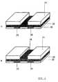
- Figs. 2a and 2brepresent the configuration of device according to the present invention.
- Fig. 3represents an interdigitated source-drain electrodes configuration.
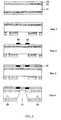
- Fig. 4represents process flow and device configuration according to the preferred embodiment of the present invention.
- a device for detecting an analyte in a sample, based on organic materialsis described.
- the devicecan be a chemically sensitive field-effective transistor (CHEMFET).
- Said deviceis a thin film transistor in which the gate electrode is missing and which comprises an active layer.
- Said active layercomprises at least a dielectric layer which is exposed to a sample comprising an analyte to be investigated directly or via a layer with a specific recognition function.
- Said devicecan be used for e.g. the detection and measuring of concentrations and activities of chemical species (analyte) present in the sample.
- Analyteshall be understood as any chemical molecule, atom or ion comprising but not limited to ions, neutral molecules and biomolecules like enzymes, immunochemicals, hormones and reducible gases.
- Sampleshall be understood as a solution, solid, gas, vapour or a mixture of those comprising at least the analyte.
- detectingshall mean determining, identification, measuring of concentrations or activities, measuring a change of concentrations or activities of at least one analyte present in the sample.
- said devicecan be used for the detection of analytes in samples in the biochemical and pharmaceutical field.
- said devicecan be used for the detection in samples containing specific analytes e.g. vapours, odour, gases.
- a device for detecting an analyte in a samplecomprising a semiconductor layer, a source electrode, a drain electrode and an active layer.
- the active layercomprises at least a dielectric material.
- the semiconducting lavercan be chosen such that it acts as current path between source and drain electrode.
- the electric field in the channel of the deviceis modified by the interaction of said active layer with an analyte in a sample.
- the choice of said semiconducting materialcan be further based on the conductivity of the material, the stability of the material, their availability, their compatibility with standard processing steps as used in the manufacturing of integrated circuits, their deposition characteristics and their cost price.
- Said semiconducting layercan be adjacent to the active layer or can not be adjacent to the active layer.
- the semiconducting layercomprises an organic containing semiconducting material.
- the organic containing semiconducting materialcan be used in its neutral (undoped) state and can be a p-type semiconductor or an n-type semiconductor but preferably a p-type semiconductor.
- Said organic containing semiconducting materialcan be an organic polymer e.g. a conjugated polymers.
- Said conjugated polymercan be but is not limited to Polythiophene (PT), poly(p-phenylene) (PPP), poly(p-phenylene vinylene) (PPV), poly(2,5-thiophene vinylene) (PTV), polypyrrole (PPy) or C 60 -buckminster fullerene.
- the organic containing semiconducting layercan also be a conducting oligomer layer wherein said oligomer layer can be but is not limited to ⁇ - hexylthiophene ( ⁇ -6T), pentacene and oligophenylene vinylene.
- the deposition of the organic containing semiconducting layercan be done by spin-coating, casting or evaporation of solution processible long-chain polymer or oligomer evaporation. Problems mentioned in the prior-art related to the deposition of electroconducting polymers are avoided by using the above mentioned deposition techniques.
- a device for detecting an analyte in a samplecomprising a semiconductor layer, a source electrode, a drain electrode and an active layer.
- the active layeris chosen such that it assures the field-effect generation and thus the current flowing in the transistor channel.
- the active layercomprises at least a dielectric material.
- the active layerconsists of a dielectric layer or a dielectric layer covered with an analyte-specific membrane.
- the dielectric capacitanceis preferably as high as possible. This can be achieved by depositing the dielectric material in very thin layers and by using materials with a high dielectric constant.
- the thickness of the layersis typically from 0.1 ⁇ up to 0.5 ⁇ .
- the dielectric constant, ⁇ , of the dielectric materialis higher than 3, and preferably higher than 5 and preferably higher than 10 and preferably higher than 100.
- the water absorption of the active layeris preferably as low as possible and preferably negligible.
- the drift of the devicecan be avoided or at least reduced by using a dielectric layer which is inert to the sample.
- Inertshall, at least for the purpose of this application, mean that the capacitance of the dielectric layer without functionalisation remain practically constant.
- organic containing semiconducting materialshave a large density of trapping levels in the band gap, a dielectric material with a high ⁇ value will reduce the operational voltage. This is an significant advantage compared to the prior art for devices with a specific sensing function such as the CHEMFET devices.
- the dielectric layercan be chosen such that it has a specific sensitivity towards the chemical species which must be detected or measured.
- the dielectric layercan comprise an organic containing dielectric material or an inorganic containing dielectric material.
- the surface of the dielectric layermust be functionalised.
- Functionalisationmeans that the chemical properties of the dielectric material in contact with the sample are modified in such a way that there is an interaction between the analyte and the modified dielectrical material.
- the functionalisationdepends on the nature of the analyte to detect.
- the analyte which has to be detectedcan be, but is not limited to an ion, an organic biomolecule or metabolic biomolecules.
- ion-selective groupsare synthesised on e.g. a polymer or an oligomer.
- the ion-selective groupscan be selected from the group comprising e.g. a crown-ether, a cryptand, or any other ion-complex forming chemical group.
- Organic biomoleculescan be detected via e.g. an enzymatic reaction, that leads to a change in e.g. the pH. This pH change will be used for the detection and measuring of the enzymatic reaction.
- the same principleis used for monitoring the cellular metabolism when the enzymatic layer is replaced by a layer of cells.
- the recognition moleculecan be entrapped in a matrix of the dielectric material.
- the dielectric materialcan also comprise an inorganic containing material.
- Said inorganic containing materialcan comprise an inorganic oxide, an inorganic nitride or an inorganic oxynitride.
- Said inorganic containing materialcan comprise an amorphous metallic material selected from the group comprising TiO 2 , BaTiO 3 , Ba x Sr 1-x TiO 3 , Pb(Zr x T 1-x )O 3 , Ta 2 O 5 , SrTiO 3 , BaZrO 3 , PbTiO 3 , LiTaO 3 etc .
- the inorganic containing materialhas a specific recognition function towards the analyte, the dielectric layer is exposed directly to the analyte.
- protons or concentrations of protonscan be detected or measured by direct exposure of the dielectric layer to the sample containing the analyte.
- the organic or inorganic containing dielectric layercan also show no specific recognition function towards the analyte.
- an analyte-specific membraneis deposited on the dielectric layer.
- the membrane layeris made of an active material.
- the analyte specific membranecan be a polymeric matrix which contains the specific recognition molecule. Possible polymeric materials and specific recognition molecules are given in G. Harsányi, Polymer Films in Sensor Applications - Technology, Materials, Devices and Their Characteristics, TECHNOMIC Publishing Co. Inc. Lancaster-Basel, 1995, pp.2. and W. Gopel, J. Hesse, J. N. Zemel, Sensors: A Comprehensive Survey, Vol.2, Part.I, 1991, pp.467-528.
- the analyte specific membranecan be but is not limited to a PVC matrix, polysiloxane-based membranes and Langmuir-Blodgett films.
- Said specific recognition moleculecan be, but is not limited to valinomycin for K + detection, specific enzymes for detecting organic inactive species (glucose, cholesterol).
- a device for detecting an analyte in a samplecomprising a source electrode, a drain electrode, a semiconductor layer and an active layer.
- the source electrode and the drain electrodecan be made of an organic containing material.
- the organic containing materialcan be chosen such that the conductivity of the material is in the metallic range.
- the surface resistance of the electrodesis preferably lower than 100 ⁇ /sq. Electrodes made of organic containing material are preferred because this results in an optimal quality of the contact between the electrodes and the organic containing semiconducting layer.
- Said organic containing materialcan be a polymer or an oligomer.
- the polymercan be but is not limited to polyaniline doped with camphor sulphonic acid.
- the source and drain electrodecan also be made of a metal like gold, platinum or aluminium, depending on the HOMO and LUMO energy levels in the organic semiconductor.
- the source and drain electrodesare preferably patterned lithographycally.
- the source and drain electrodescan have an interdigitated configuration, as it is illustrated in figure 3, in order to achieve maximum electric current flowing into the transistor channel.
- the channel width (1)-to-length (2) ratio, and the number of fingersmust be optimised in order to achieve the desired level for the output current. This configuration is preferred because of the low conductance of the organic containing semiconductor material.
- said devicefurther comprises a support layer.
- the support layeris chosen such that it assures the deposition of the active layers and that it maintains the flatness of the device.
- the supportcan be made of polymeric material with a high chemical resistance and thermal properties which are determined by the further deposition steps.
- the upper working temperature of said support layeris higher than 100 °C, higher than 150 °C or preferably higher than 300 °C.
- Such materialcan be polyvinyldifluoride, high density polyethylene, polyimide, polytetrafluoroethylen (teflonTM), polypropylene or any other material which fulfils the above mentioned properties.
- the devicecan be encapsulated by an encapsulating layer.
- the semiconducting layer and the electrodesare encapsulated such that the current pathway between source and drain electrode in the semiconducting layer is protected from the air and from the sample.
- the encapsulating layercan be made, but is not limited to an epoxy resin (such as EP42HT, purchased from Master Bond Inc.) or parylene.
- FIG. 2Brepresents a device for detecting an analyte in a sample according to the present invention.
- Said devicecan be a chemical selective field-effect transistor.
- a methodis disclosed which can be used for the manufacturing of a single sensor or an array of sensors.
- Such sensor arrayhas a multitude of sensing sites, each sensing site being a sensor.
- the inert support layeris a common support layer of the array.
- the dielectric materialis an inorganic oxide and can be selected from the inorganic oxides mentioned above.
- the dielectric layeris deposited by RF sputtering at a temperature range from 5 °C to 50 °C and preferably at room temperature.
- the thickness of the dielectric layeris preferably about 0.1 ⁇ .
- the source and drain electrodeare deposited.
- a layer of an organic containing materiale.g. doped polyanaline with camphorsulfonic acid, is deposited on the dielectric layer.
- the layerwill be patterned lithographycally such that the source electrode (23) and the drain electrode (24) are formed.
- the organic containing semiconducting layer (25)is deposited on both electrodes and on the remaining dielectric layer.
- the semiconducting layerhas preferably a thickness between 0.1 and 0.5 ⁇ m and is deposited by spin-coating.
- An encapsulating layeris formed such that the source and drain electrodes and the semiconducting layer are protected from air and from the sample.
- an analyte specific membrane (26)is deposited on the dielectric layer and adjacent to holes formed in the support layer. The composition of the membrane depends on the nature of the analyte to detect.
- the temperature range for all processing stepsis as low as possible and preferably lower than 300 °C.
- the device as describedcan be used with or without a reference electrode.
- a reference electrode or a reference FETcan be used, depending on the measurement method.
- the chemical environmente.g. aqueous solution
- the electric current flowing between source and drain electrodesis recorded in function of the changes in the chemical environment of the sensor.
- the voltage drop between the source electrodewhich is usually grounded
- the constant drain current modethe current between source and drain is kept constant by adjusting the voltage drop V GS between the reference electrode or reference FET and the source electrode.
- the response of the sensoris the variation of this voltage drop, V GS , in function of the changes in the chemical environment.
- the silicon wafer (51) with a thickness of 650 ⁇ mis used as a support for device. This is only a mechanical support structure and does not perform an active role in the device operation.
- Two layers of silicon oxide (470 nm) (53) and silicon nitride (150 nm) (52), respectively,have been deposited on the both side of the silicon wafer, as can be seen from the figure 4. The thickness of these two layers has been chosen to reduce the mechanical stress in the membrane.
- the silicon oxide layerhas the function of reducing the mechanical stress.
- the silicon nitride layerperforms a double role in this case: it represents the active layer (being dielectric sensitive gate) and, at the same time, it is a stopping layer for the anisotropic KOH etching.
- FIG 4The processing steps are illustrated in figure 4.
- the gold source (54) and drain (55) interdigitated electrodes with a thickness of 100 nmwere deposited by thermal evaporation and patterned by lift-off technique (figure 4 - step 2).
- the P3HT (poly-3-hexyl thiophene) semiconducting layer (56)was spin-coated onto the electrodes from a chloroform solution with a concentration of 0.8 % weight (figure 4 - step 3).
- the window defining the sensitive areawas made by etching completely the silicon in KOH 35% weight solution in water at 40 °C (figure 4 - step 4). This delimitates an active area of 1 mm x 1 mm on the silicon nitride surface.
- the resulting devicewas wire-bonded on a thick-film alumina substrate and encapsulated with EP42HT, a two-component epoxy that cures at room temperature, purchased from Master Bond Inc.
Landscapes
- Life Sciences & Earth Sciences (AREA)
- Chemical & Material Sciences (AREA)
- Health & Medical Sciences (AREA)
- Physics & Mathematics (AREA)
- Molecular Biology (AREA)
- Microelectronics & Electronic Packaging (AREA)
- Chemical Kinetics & Catalysis (AREA)
- Electrochemistry (AREA)
- Engineering & Computer Science (AREA)
- Analytical Chemistry (AREA)
- Biochemistry (AREA)
- General Health & Medical Sciences (AREA)
- General Physics & Mathematics (AREA)
- Immunology (AREA)
- Pathology (AREA)
- Investigating Or Analyzing Materials By The Use Of Electric Means (AREA)
Description
- The present invention is related to a devicefor detecting an analyte in a sample belonging to a classof devices known as chemically-sensitive field-effecttransistors (CHEMFET's) which are of particular interestfor biomedical and industrial applications.
- There is considerable interest in methods fordetection, measuring and monitoring chemical properties ofa sample. A sample can be a solid, solution, gas, vapour ora mixture of those. The chemical properties of the sampleare determined by the analyte present in the sample, theanalyte can be e.g. an electrolyte, a biomolecule or aneutral molecule.
- Chemical sensors belonging to a class ofdevices known as Chemically Sensitive Field-EffectTransistors (CHEMFET's) are of particular interest forbiomedical and industrial applications. Chemicallysensitive field-effect transistors measure chemicalproperties of the samples to which the device is exposed.In a CHEMFET, the changes at the surface of the gatedielectric are detected via the modulations of the electricfield in the channel of a field-effect transistor. Suchchemical changes can be induced by e.g. the presence of ions in aqueous solutions, but also by the interaction ofan electroinactive organic compound with a biological-sensingelement in contact with the gate of the field-effecttransistor. In this way, the concentration of ionsor organic biomolecules (e.g. glucose, cholesterol, etc) inaqueous solutions can be measured. One promisingapplication of this type of device regards the monitoringof the cell metabolism for fundamental research or drug-characterisationstudies.
- Among CHEMFET devices, the ion-sensitivefield-effect transistors are best known. The concept ofion-sensitive field-effect transistor (ISFET) has beenintroduced by P. Bergveld in 1970 [P. Bergveld,IEEE Trans.Biomed. Eng., BME-17, 1970, pp. 70]. It was demonstratedthat when the metal gate of an ordinary MOSFET is omittedand the dielectric layer is exposed to an electrolyte, thecharacteristics of the transistor are affected by the ionicactivity of the electrolyte. The schematic drawing of aclassic ISFET is shown in figure 1. The siliconsubstrate(1) of the device acts as current pathway betweenthe source region (3) and the drain region (2). Bothregions are contacted by metal electrodes (5). Thedielectric layer (4) is covered with an ion-selectivemembrane (6) which is exposed to the solution (7). Thedevice is encapsulated with an encapsulating material (9).Optionally, a reference electrode (8) can be present.
- ISFET's have first been developed for pH andNa+ activity detection in aqueous solutions (C. D. Fung,P.W. Cheung and W. H. Ko,IEEE Trans. El. Dev., Vol. ED-33,No.1, 1986, pp. 8-18). The cation-sensitivity of the deviceis determined by the ionisation and complexation of thesurface hydroxyl groups on the gate dielectric surface.ISFET devices for Ca2+, K+ activity monitoring have also been fabricated. The sensitivity towards these ions isachieved by incorporating a sensitised plastic membrane(PVC) in contact with the gate dielectric. Therefore, thesesensors detect changes in the charge of the membrane or inthe transmembranar potential. Besides the use of CHEMFETdevices for the determination of ions (ISFET), CHEMFET'shave also been employed as enzyme-sensitive FET (ENFET's)for organic molecule detection or immuno-sensitive FET's(IMFET's) for immunochemicals (antigen, antibody)monitoring.
- CHEMFET's exhibit important advantages overconventional chemically selective electrodes. Usually,CHEMFET's are fabricated with standard CMOS technology,which offers the advantages of miniaturisation and massproduction. In the biomedical field, there is an especiallyimportant area for the application of miniaturised sensors.The sensor is mounted in the tip of indwelling catheters,through which their feasibility for monitoring bloodelectrolytes and parameters has been demonstrated.
- The fabrication method offers the additionalbenefit of the fabrication of multi-ion sensors andintegration in smart sensors and sensor arrays. A furtheradvantage of the use of CHEMFET is the logarithmic responseof the potential in function of the analyte concentration,this type of response is interesting if a broadconcentration range is investigated. Since the response ofa CHEMFET device is initiated by the field-effect, thisresponse is very fast compared to the response ofconventional chemically sensitive electrodes. Up to now,all CHEMFET devices are based on silicon or silicon basedmaterials.
- However, there are some problems that so farhave hampered the commercial applications of these devices.The most important problem of the CHEMFET is the drift of the device. Drift is typically characterised by arelatively slow, monotonic temporal change in the thresholdvoltage of the FET. As a result, an incorrect estimation ofthe chemical properties (e.g. ion activity) of the samplewill be determined. This problem is more pronounced fordetermination of e.g. physiological ion activities orconcentrations, where a high accuracy is required (e.g.blood electrolytes monitoring). Therefore, the use ofsilicon-based CHEMFET's in this kind of applications isvery reduced. A further limiting factor for the use ofCHEMFET devices is the higher manufacturing cost of thesedevices. For medical application, one is mostly interestedin throw-away devices, which implies very cheap devices.For medical and pharmaceutical applications, devices thatcan be integrated in plastic materials, are most suitable.
- For silicon-based CHEMFET, the integration inplastic material is not straightforward.
- In the prior art, thin film transistors basedon organic materials have been fabricated. Garnier (GarnierF., Hajlaoui R., Yassar A., Srivastava P., Science, 1994,Vol. 265, p 1684) proposes the use polymeric materials in athin film transistor. The choice of polymeric materials isdetermined by the application of the device, i.e. astransistor.
- Organic materials, and more especiallypolymeric materials, have already been used as sensitiveparts in combination with a solid-state transducer(inorganic material) or as membranes for immobilisation ofbiomolecules (e.g. enzymes) for specific interactions (G.Harsányi,Polymer Films in Sensor Applications -Technology, Materials, Devices and Their Characteristics,TECHNOMIC Publishing Co. Inc. Lancaster-Basel, 1995, p 53-92and p 149-155; G. Bidan,Sensors and Actuators B,
Vol 6,1992, pp. 45-56). In the electroconducting conjugated polymers-based (ECP-based) chemical sensors, there is adirect interaction between the EPC layer and the analyte todetect. The detection mechanism is based on the ionexchange between the ECP layer and the sample. Therefore, adoped ECP layer is needed. A major disadvantage is therequired electrochemical deposition of the conductinglayer, because this deposition technique is ratherdifficult to control, which results in the deposition oflayers with a lower uniformity and reproducibility.Moreover, the electrochemical deposition of dopedconjugated polymeric layers also implies a morecomplicated, multi-step process. Besides this, due to theelectropolymerisation reactions, the electroconductingconjugated polymer layer is always p-doped, which meansthat only anions can be detected. Furthermore, thedeposition process requires electrodes made of metallicmaterial or glassy carbon. - The present invention aims to provide animproved device for detecting an analyte in a sample whichcombines the advantages of existing CHEMFET devices withadvantageous properties such as low price, disposability,reduced drift of the device and suitability for biomedicaland pharmaceutical applications.
- A device for detecting an analytein a sample according to the inventionis recited in
claim 1. - In a first aspect of this invention, a devicefor detecting an analyte in a sample is disclosedcomprising an active layer comprising at least a dielectricmaterial, a source electrode, a drain electrode and asemiconducting layer for providing a current pathwaybetween said source electrode and said drain electrode andwherein said semiconducting substrate consists of an organic containing semiconducting material and wherein saiddielectric material of said active layer is substantiallyin contact with said semicondcuting layer. The device ischaracterised in that said active layer is arranged tocontact said sample and to influence the conductance ofsaid semiconducting layer when in contact with said samplecontaining said analyte to detect,. Said Analyte, as usedherein, shall be understood as any chemical molecule, atomor ion comprising but not limited to ions, neutralmolecules and biomolecules like enzymes, immunochemicals,hormones and reducible gases. Sample, as used herein, shallbe understood as a solid, solution, gas, vapour or amixture of those comprising at least the analyte. For thepurpose of this invention, detecting shall meandetermining, identification, measuring of concentrations oractivities, measuring a change of concentrations oractivities of at least one analyte present in the sample.
- In an embodiment of the invention, the activelayer comprises a dielectric layer.
- In an embodiment of this invention, thedielectric layer consists of a material with a dielectricconstant higher than 3. In order to maximise the currentflow between source and drain, the value of the dielectricconstant must be as high as possible. Furthermore, adielectric material with a high value of the dielectricconstant will reduce the operational voltage of the device.
- The chemically selective dielectric layer canbe chosen such that the material of the dielectric layer isessentially inert to the sample. Inert shall, at least forthe purpose of this application, means that the capacitanceof the dielectric layer without functionalisation remainpractically constant. Thus, the problems related to thedrift of the device can be eliminated. The drift phenomenais typically observed for silicon-based devices, since the silicon layer can be modified when exposed to the sample,resulting in a change of the capacitance of the dielectriclayer. This results in slow, temporal change in thethreshold voltage, which implies an incorrect estimation ofthe detection of the analyte.
- In an embodiment of the invention, the activelayer consists essentially of a dielectric layer. Thedielectric layer is made of an active material arranged toselectively react with said analyte when said device isexposed to said sample containing said analyte. Dependingon the application, the dielectric layer which is exposedto the sample can be modified in such a way that there isan interaction between the analyte and the modifieddielectrical material.
- In an embodiment of the invention, thedielectric layer comprises an organic dielectric material.In a further embodiment of the invention, the dielectriclayer comprises an inorganic containing material. The valueof the dielectric capacitance is preferably as high aspossible. The value of the dielectric constant, ε, of thedielectric material is higher than 3, and preferably higherthan 5 and preferably higher than 10 and preferably higherthan 100.
- In a further embodiment of the invention, theactive layer can further comprises a dielectric layer and amembrane layer. Said membrane layer is made of activematerial and is arranged to selectively react with saidanalyte when the device is exposed to the sample containingthe analyte. Preferably, the chemically sensitive membraneis a conjugated oligomer or a polymer.
- In a further embodiment of the first aspectof the invention, the source and drain electrode comprisean organic containing material characterised in that said the surface resistance of the electrodes is lower than100Ω/sq. The source and drain electrode can have aninterdigitated configuration.
- In a further embodiment of this invention,the device can additionally comprise an encapsulating layerto protect said current pathway between said sourceelectrode and said drain electrode and a a support layerwherein said encapsulating layer and support layer are madeof organic containing material.
- In a second aspect of this invention, asystem for detecting an analyte in a sample is disclosed,comprising a device as described in the first aspect ofthis invention, and a reference field-effect transistor.
- Fig. 1 represents a description of an ion-sensitivefield-effect transistor (ISFET) fabricated withCMOS technology (H. H. van den Vlekkert et. al.,Proc. 2ndInt. Meeting on Chemical Sensors, Bordeaux, France,1986,pp. 462.)
- Figs. 2a and 2b represent the configurationof device according to the present invention.
- Fig. 3 represents an interdigitated source-drainelectrodes configuration.
- Fig. 4 represents process flow and deviceconfiguration according to the preferred embodiment of thepresent invention.
- In relation to the appended drawings thepresent invention is described in detail in the sequel.Several embodiments are disclosed. It is apparent howeverthat a person skilled in the art can imagine several other equivalent embodiments or other ways of practising thepresent invention, the scope thereof beinglimited only by the terms of the appended claims.
- A device for detecting an analyte in asample, based on organic materials is described. The devicecan be a chemically sensitive field-effective transistor(CHEMFET). Said device is a thin film transistor in whichthe gate electrode is missing and which comprises an activelayer. Said active layer comprises at least a dielectriclayer which is exposed to a sample comprising an analyte tobe investigated directly or via a layer with a specificrecognition function. Said device can be used for e.g. thedetection and measuring of concentrations and activities ofchemical species (analyte) present in the sample. Analyte,as used herein, shall be understood as any chemicalmolecule, atom or ion comprising but not limited to ions,neutral molecules and biomolecules like enzymes,immunochemicals, hormones and reducible gases. Sample, asused herein, shall be understood as a solution, solid, gas,vapour or a mixture of those comprising at least theanalyte. For the purpose of this invention, detecting shallmean determining, identification, measuring ofconcentrations or activities, measuring a change ofconcentrations or activities of at least one analytepresent in the sample. Particularly, said device can beused for the detection of analytes in samples in thebiochemical and pharmaceutical field. Furthermore, saiddevice can be used for the detection in samples containingspecific analytes e.g. vapours, odour, gases.
- In this invention, a device for detecting ananalyte in a sample is disclosed, comprising asemiconductor layer, a source electrode, a drain electrodeand an active layer. The active layer comprises at least adielectric material. The semiconducting laver can be chosen such that it acts as current path between source and drainelectrode. The electric field in the channel of the deviceis modified by the interaction of said active layer with ananalyte in a sample. The choice of said semiconductingmaterial can be further based on the conductivity of thematerial, the stability of the material, theiravailability, their compatibility with standard processingsteps as used in the manufacturing of integrated circuits,their deposition characteristics and their cost price.
- Said semiconducting layer can be adjacent tothe active layer or can not be adjacent to the activelayer.
- The direct interaction of the semiconducting layerwith the analyte is preferably negligible. In thisinvention, the semiconducting layer comprises an organiccontaining semiconducting material. The organic containingsemiconducting material can be used in its neutral(undoped) state and can be a p-type semiconductor or an n-typesemiconductor but preferably a p-type semiconductor.Said organic containing semiconducting material can be anorganic polymer e.g. a conjugated polymers. Said conjugatedpolymer can be but is not limited to Polythiophene (PT),poly(p-phenylene) (PPP), poly(p-phenylene vinylene) (PPV),poly(2,5-thiophene vinylene) (PTV), polypyrrole (PPy) orC60-buckminster fullerene. The organic containingsemiconducting layer can also be a conducting oligomerlayer wherein said oligomer layer can be but is not limitedto α - hexylthiophene (α-6T), pentacene and oligophenylenevinylene.
- The deposition of the organic containingsemiconducting layer can be done by spin-coating, castingor evaporation of solution processible long-chain polymeror oligomer evaporation. Problems mentioned in the prior-art related to the deposition of electroconducting polymersare avoided by using the above mentioned depositiontechniques.
- In this invention, a device for detecting ananalyte in a sample is disclosed, comprising asemiconductor layer, a source electrode, a drain electrodeand an active layer.
- Said active layer is chosen such that itassures the field-effect generation and thus the currentflowing in the transistor channel. The active layercomprises at least a dielectric material. Preferably, theactive layer consists of a dielectric layer or a dielectriclayer covered with an analyte-specific membrane. In orderto maximise the current flowing between source and drain,the dielectric capacitance is preferably as high aspossible. This can be achieved by depositing the dielectricmaterial in very thin layers and by using materials with ahigh dielectric constant. The thickness of the layers istypically from 0.1µ up to 0.5 µ. The dielectric constant,ε, of the dielectric material is higher than 3, andpreferably higher than 5 and preferably higher than 10 andpreferably higher than 100. The water absorption of theactive layer is preferably as low as possible andpreferably negligible.
- The drift of the device, as mentioned in thebackground of the invention can be avoided or at leastreduced by using a dielectric layer which is inert to thesample. Inert shall, at least for the purpose of thisapplication, mean that the capacitance of the dielectriclayer without functionalisation remain practicallyconstant. Moreover, taking into account that organiccontaining semiconducting materials have a large density oftrapping levels in the band gap, a dielectric material with a high ε value will reduce the operational voltage. This isan significant advantage compared to the prior art fordevices with a specific sensing function such as theCHEMFET devices.
- The dielectric layer can be chosen such thatit has a specific sensitivity towards the chemical specieswhich must be detected or measured. The dielectric layercan comprise an organic containing dielectric material oran inorganic containing dielectric material.
- When the dielectric layer comprises anorganic containing material and in order to achieve thespecific chemical sensitivity, the surface of thedielectric layer must be functionalised. Functionalisationmeans that the chemical properties of the dielectricmaterial in contact with the sample are modified in such away that there is an interaction between the analyte andthe modified dielectrical material. The functionalisationdepends on the nature of the analyte to detect. The analytewhich has to be detected can be, but is not limited to anion, an organic biomolecule or metabolic biomolecules. Whenthe analyte is an ion, ion-selective groups are synthesisedon e.g. a polymer or an oligomer. For the detection of ionslike Na+, K+, Ca2+, Mg2+, Cl- or any other ion, the ion-selectivegroups can be selected from the group comprisinge.g. a crown-ether, a cryptand, or any other ion-complexforming chemical group. Organic biomolecules can bedetected via e.g. an enzymatic reaction, that leads to achange in e.g. the pH. This pH change will be used for thedetection and measuring of the enzymatic reaction. The sameprinciple is used for monitoring the cellular metabolismwhen the enzymatic layer is replaced by a layer of cells.Also, the recognition molecule can be entrapped in a matrixof the dielectric material.
- The dielectric material can also comprise aninorganic containing material. Said inorganic containingmaterial can comprise an inorganic oxide, an inorganicnitride or an inorganic oxynitride. Said inorganiccontaining material can comprise an amorphous metallicmaterial selected from the group comprising TiO2, BaTiO3,BaxSr1-xTiO3, Pb(ZrxT1-x)O3, Ta2O5, SrTiO3, BaZrO3, PbTiO3,LiTaO3 etc . When the inorganic containing material has aspecific recognition function towards the analyte, thedielectric layer is exposed directly to the analyte. Fore.g. an inorganic oxide, protons or concentrations ofprotons can be detected or measured by direct exposure ofthe dielectric layer to the sample containing the analyte.
- The organic or inorganic containingdielectric layer can also show no specific recognitionfunction towards the analyte. Therefor, an analyte-specificmembrane is deposited on the dielectric layer. The membranelayer is made of an active material. The analyte specificmembrane can be a polymeric matrix which contains thespecific recognition molecule. Possible polymeric materialsand specific recognition molecules are given in G.Harsányi,Polymer Films in Sensor Applications -Technology, Materials, Devices and Their Characteristics,TECHNOMIC Publishing Co. Inc. Lancaster-Basel, 1995, pp.2.and W. Gopel, J. Hesse, J. N. Zemel,Sensors: AComprehensive Survey, Vol.2, Part.I, 1991, pp.467-528. Theanalyte specific membrane can be but is not limited to aPVC matrix, polysiloxane-based membranes and Langmuir-Blodgettfilms. Said specific recognition molecule can be,but is not limited to valinomycin for K+ detection,specific enzymes for detecting organic inactive species(glucose, cholesterol).
- In this invention, a device for detecting ananalyte in a sample is disclosed, comprising a sourceelectrode, a drain electrode, a semiconductor layer and anactive layer.
- The source electrode and the drain electrodecan be made of an organic containing material. The organiccontaining material can be chosen such that theconductivity of the material is in the metallic range. Thesurface resistance of the electrodes is preferably lowerthan 100Ω/sq. Electrodes made of organic containingmaterial are preferred because this results in an optimalquality of the contact between the electrodes and theorganic containing semiconducting layer. Said organiccontaining material can be a polymer or an oligomer. Thepolymer can be but is not limited to polyaniline doped withcamphor sulphonic acid. The source and drain electrode canalso be made of a metal like gold, platinum or aluminium,depending on the HOMO and LUMO energy levels in the organicsemiconductor. The source and drain electrodes arepreferably patterned lithographycally. The source and drainelectrodes can have an interdigitated configuration, as itis illustrated in figure 3, in order to achieve maximumelectric current flowing into the transistor channel. Thechannel width (1)-to-length (2) ratio, and the number offingers must be optimised in order to achieve the desiredlevel for the output current. This configuration ispreferred because of the low conductance of the organiccontaining semiconductor material.
- In a further embodiment of the presentinvention, said device further comprises a support layer.The support layer is chosen such that it assures thedeposition of the active layers and that it maintains theflatness of the device. The support can be made of polymeric material with a high chemical resistance andthermal properties which are determined by the furtherdeposition steps. The upper working temperature of saidsupport layer is higher than 100 °C, higher than 150 °C orpreferably higher than 300 °C. Such material can bepolyvinyldifluoride, high density polyethylene, polyimide,polytetrafluoroethylen (teflon™), polypropylene or anyother material which fulfils the above mentionedproperties.
- Furthermore, the device can be encapsulatedby an encapsulating layer. The semiconducting layer and theelectrodes are encapsulated such that the current pathwaybetween source and drain electrode in the semiconductinglayer is protected from the air and from the sample. Theencapsulating layer can be made, but is not limited to anepoxy resin (such as EP42HT, purchased from Master BondInc.) or parylene.
- An embodiment of the invention is given infigure 2B. Fig. 2B represents a device for detecting ananalyte in a sample according to the present invention.Said device can be a chemical selective field-effecttransistor. Besides the structure of the CHEMFET, a methodis disclosed which can be used for the manufacturing of asingle sensor or an array of sensors. Such sensor array hasa multitude of sensing sites, each sensing site being asensor. In a preferred embodiment, the inert support layeris a common support layer of the array.
- A support substrate (21) selected accordingto the further processing steps as known in the integratedcircuit manufacturing. In a next step, a dielectric layer(22) deposited on the support layer. The dielectricmaterial is an inorganic oxide and can be selected from theinorganic oxides mentioned above. The dielectric layer is deposited by RF sputtering at a temperature range from 5 °Cto 50 °C and preferably at room temperature. The thicknessof the dielectric layer is preferably about 0.1 µ. In anext step, the source and drain electrode are deposited.First, a layer of an organic containing material, e.g.doped polyanaline with camphorsulfonic acid, is depositedon the dielectric layer. Subsequently, the layer will bepatterned lithographycally such that the source electrode(23) and the drain electrode (24) are formed. Then, theorganic containing semiconducting layer (25) is depositedon both electrodes and on the remaining dielectric layer.The semiconducting layer has preferably a thickness between0.1 and 0.5 µm and is deposited by spin-coating. Anencapsulating layer is formed such that the source anddrain electrodes and the semiconducting layer are protectedfrom air and from the sample. In a last step, an analytespecific membrane (26) is deposited on the dielectric layerand adjacent to holes formed in the support layer. Thecomposition of the membrane depends on the nature of theanalyte to detect.
- Since organic containing materials is areinvolved in the most processing steps, the temperaturerange for all processing steps is as low as possible andpreferably lower than 300 °C.
- In a further embodiment of this invention, astructure as represented in figure 2A is disclosed.
- The device as described can be used with orwithout a reference electrode. A reference electrode or areference FET can be used, depending on the measurementmethod. For instance, in the fixed gate voltage mode, thechemical environment (e.g. aqueous solution) is kept at afixed potential in respect to the sensor source electrode,and the electric current flowing between source and drain electrodes is recorded in function of the changes in thechemical environment of the sensor. This is realised byadjusting the voltage drop between the source electrode(which is usually grounded) and a reference electrode orreference FET. Also, in the constant drain current mode,the current between source and drain is kept constant byadjusting the voltage drop VGS between the referenceelectrode or reference FET and the source electrode. Theresponse of the sensor is the variation of this voltagedrop, VGS, in function of the changes in the chemicalenvironment.
- In the preferred embodiment, a device asdepicted in figure 4 is disclosed.
- The silicon wafer (51) with a thickness of650 µm is used as a support for device. This is only amechanical support structure and does not perform an activerole in the device operation. Two layers of silicon oxide(470 nm) (53) and silicon nitride (150 nm) (52),respectively, have been deposited on the both side of thesilicon wafer, as can be seen from the figure 4. Thethickness of these two layers has been chosen to reduce themechanical stress in the membrane. The silicon oxide layerhas the function of reducing the mechanical stress. Thesilicon nitride layer performs a double role in this case:it represents the active layer (being dielectric sensitivegate) and, at the same time, it is a stopping layer for theanisotropic KOH etching.
- The processing steps are illustrated infigure 4. First a mask was patterned, by means ofconventional lithography and dry etching, in the back sideoxide and nitride layers to define the active area (57) andthe "V" grooves (58) that are used for easy cleavage (seefigure 4 - step 1). Subsequently, the gold source (54) and drain (55) interdigitated electrodes with a thickness of100 nm were deposited by thermal evaporation and patternedby lift-off technique (figure 4 - step 2). In the nextstep, the P3HT (poly-3-hexyl thiophene) semiconductinglayer (56) was spin-coated onto the electrodes from achloroform solution with a concentration of 0.8 % weight(figure 4 - step 3). The window defining the sensitive areawas made by etching completely the silicon in KOH 35%weight solution in water at 40 °C (figure 4 - step 4). Thisdelimitates an active area of 1 mm x 1 mm on the siliconnitride surface.
- After cleavage, the resulting device waswire-bonded on a thick-film alumina substrate andencapsulated with EP42HT, a two-component epoxy that curesat room temperature, purchased from Master Bond Inc.
Claims (16)
- A device for detecting an analyte in asample comprising:an active layer consisting of a dielectric material (22),and optionally of an analyte-specific-membrane (26),a source electrode (23), a drain electrode (24) and nogate electrode,a semiconducting layer (25) for providing a currentpathway between said source electrode (23) and said drainelectrode (24), wherein:said semiconducting layer (25) consists of an organicsemiconducting material,said dielectric material (22) of said active layer is incontact with said semiconducting layer (25), andsaid active layer is arranged to contact said sample andto influence the conductance of said semiconducting layer (25)when in contact with said sample containing said analyte.
- A device as recited in claim 1 wherein saiddielectric material (22) consists of a material with adielectric constant higher than 3 or higher than 5.
- A device as recited in any of claim 1 or 2wherein said dielectric material (22) is an organic containingmaterial.
- A device as recited in claim 3 wherein saiddielectric constant of said organic containing material has avalue higher than 8.
- A device as recited in claim 1 or 2 whereinsaid dielectric layer (22) is an inorganic containingmaterial.
- A device as recited in claim 5 wherein saiddielectric constant of said inorganic containing material hasa value higher than 10;
- A device as recited in claim 5 or 6 whereinsaid dielectric layer (22) comprises an amorphous metallicmaterial selected from the group consisting of TiO2, BaTiO3,BaxSr1-xTiO3, Pb(ZrxT1-x)O3, Ta2O5, SrTiO3, BaZrO3, PbTiO3,LiTaO3.
- A device as recited in any of claims 1 to 7wherein said organic semiconducting material (22) comprises aconjugated oligomer or polymer.
- A device as recited in claim 8 wherein saidpolymer or said oligomer is selected from the group consistingof Polythiophene, poly(p-phenylene), poly (p-phenylenevinylene), poly(2,5-thiophene vinylene),polypyrrole (PPy), α-hexylthiophene, pentacene andoligophenylene vinylene.
- A device as recited in any of claims 1 to 9wherein said analyte-specific membrane (26) is selected fromthe group consisting of PVC matrix, polysiloxane-basedmembranes and Langmuir-Blodgett films.
- A device as recited in any of claims 1 to10 wherein said source electrode (23) and said drain electrode(24) comprise an organic containing material, the surfaceresistance of said electrodes being lower than 100 OMEGA /sq.
- A device as recited in any of claims 1 to11 wherein said source electrode (23) and said drain electrode(24) have an interdigitated configuration.
- A device as recited in any of claims 1 to12 further comprising an encapsulating layer to protect saidcurrent pathway between said source electrode (23) and saiddrain electrode (24), a support layer (21), wherein saidencapsulating layer and support layer (21) are made of organiccontaining material.
- A system for detecting an analyte in asample comprising a device as recited in any of claims 1 to 13and a reference field-effect transistor.
- An array of devices for detecting ananalyte in, a sample comprising at least one device as recitedin any of claims 1 to 14.
- Use of a device as recited in any of claims1 to 15 for detecting an analyte in a sample.
Priority Applications (1)
| Application Number | Priority Date | Filing Date | Title |
|---|---|---|---|
| EP00870200AEP1085319B1 (en) | 1999-09-13 | 2000-09-13 | A device for detecting an analyte in a sample based on organic materials |
Applications Claiming Priority (3)
| Application Number | Priority Date | Filing Date | Title |
|---|---|---|---|
| EP99870186 | 1999-09-13 | ||
| EP99870186AEP1085320A1 (en) | 1999-09-13 | 1999-09-13 | A device for detecting an analyte in a sample based on organic materials |
| EP00870200AEP1085319B1 (en) | 1999-09-13 | 2000-09-13 | A device for detecting an analyte in a sample based on organic materials |
Publications (2)
| Publication Number | Publication Date |
|---|---|
| EP1085319A1 EP1085319A1 (en) | 2001-03-21 |
| EP1085319B1true EP1085319B1 (en) | 2005-06-01 |
Family
ID=26074287
Family Applications (1)
| Application Number | Title | Priority Date | Filing Date |
|---|---|---|---|
| EP00870200AExpired - LifetimeEP1085319B1 (en) | 1999-09-13 | 2000-09-13 | A device for detecting an analyte in a sample based on organic materials |
Country Status (1)
| Country | Link |
|---|---|
| EP (1) | EP1085319B1 (en) |
Cited By (13)
| Publication number | Priority date | Publication date | Assignee | Title |
|---|---|---|---|---|
| US6916717B2 (en) | 2002-05-03 | 2005-07-12 | Motorola, Inc. | Method for growing a monocrystalline oxide layer and for fabricating a semiconductor device on a monocrystalline substrate |
| US6965128B2 (en) | 2003-02-03 | 2005-11-15 | Freescale Semiconductor, Inc. | Structure and method for fabricating semiconductor microresonator devices |
| US6992321B2 (en) | 2001-07-13 | 2006-01-31 | Motorola, Inc. | Structure and method for fabricating semiconductor structures and devices utilizing piezoelectric materials |
| US7005717B2 (en) | 2000-05-31 | 2006-02-28 | Freescale Semiconductor, Inc. | Semiconductor device and method |
| US7019332B2 (en) | 2001-07-20 | 2006-03-28 | Freescale Semiconductor, Inc. | Fabrication of a wavelength locker within a semiconductor structure |
| US7020374B2 (en) | 2003-02-03 | 2006-03-28 | Freescale Semiconductor, Inc. | Optical waveguide structure and method for fabricating the same |
| US7045815B2 (en) | 2001-04-02 | 2006-05-16 | Freescale Semiconductor, Inc. | Semiconductor structure exhibiting reduced leakage current and method of fabricating same |
| US7067856B2 (en) | 2000-02-10 | 2006-06-27 | Freescale Semiconductor, Inc. | Semiconductor structure, semiconductor device, communicating device, integrated circuit, and process for fabricating the same |
| US7105866B2 (en) | 2000-07-24 | 2006-09-12 | Freescale Semiconductor, Inc. | Heterojunction tunneling diodes and process for fabricating same |
| US7161227B2 (en) | 2001-08-14 | 2007-01-09 | Motorola, Inc. | Structure and method for fabricating semiconductor structures and devices for detecting an object |
| US7169619B2 (en) | 2002-11-19 | 2007-01-30 | Freescale Semiconductor, Inc. | Method for fabricating semiconductor structures on vicinal substrates using a low temperature, low pressure, alkaline earth metal-rich process |
| US7211852B2 (en) | 2001-01-19 | 2007-05-01 | Freescale Semiconductor, Inc. | Structure and method for fabricating GaN devices utilizing the formation of a compliant substrate |
| US7342276B2 (en) | 2001-10-17 | 2008-03-11 | Freescale Semiconductor, Inc. | Method and apparatus utilizing monocrystalline insulator |
Families Citing this family (22)
| Publication number | Priority date | Publication date | Assignee | Title |
|---|---|---|---|---|
| US6693033B2 (en) | 2000-02-10 | 2004-02-17 | Motorola, Inc. | Method of removing an amorphous oxide from a monocrystalline surface |
| US6638838B1 (en) | 2000-10-02 | 2003-10-28 | Motorola, Inc. | Semiconductor structure including a partially annealed layer and method of forming the same |
| US20020089023A1 (en)* | 2001-01-05 | 2002-07-11 | Motorola, Inc. | Low leakage current metal oxide-nitrides and method of fabricating same |
| US6673646B2 (en) | 2001-02-28 | 2004-01-06 | Motorola, Inc. | Growth of compound semiconductor structures on patterned oxide films and process for fabricating same |
| US6709989B2 (en) | 2001-06-21 | 2004-03-23 | Motorola, Inc. | Method for fabricating a semiconductor structure including a metal oxide interface with silicon |
| US6646293B2 (en) | 2001-07-18 | 2003-11-11 | Motorola, Inc. | Structure for fabricating high electron mobility transistors utilizing the formation of complaint substrates |
| US6693298B2 (en) | 2001-07-20 | 2004-02-17 | Motorola, Inc. | Structure and method for fabricating epitaxial semiconductor on insulator (SOI) structures and devices utilizing the formation of a compliant substrate for materials used to form same |
| US6855992B2 (en) | 2001-07-24 | 2005-02-15 | Motorola Inc. | Structure and method for fabricating configurable transistor devices utilizing the formation of a compliant substrate for materials used to form the same |
| US6667196B2 (en) | 2001-07-25 | 2003-12-23 | Motorola, Inc. | Method for real-time monitoring and controlling perovskite oxide film growth and semiconductor structure formed using the method |
| US6639249B2 (en) | 2001-08-06 | 2003-10-28 | Motorola, Inc. | Structure and method for fabrication for a solid-state lighting device |
| US6673667B2 (en) | 2001-08-15 | 2004-01-06 | Motorola, Inc. | Method for manufacturing a substantially integral monolithic apparatus including a plurality of semiconductor materials |
| DE10161213B4 (en)* | 2001-12-13 | 2004-02-19 | Ignaz Prof. Dr. Eisele | Gas sensor and method for the detection of one or more components of a gas mixture and / or gases in a liquid according to the principle of work function measurement |
| DE10209075A1 (en)* | 2002-03-01 | 2003-09-18 | Infineon Technologies Ag | CMOS process-compatible high-DK surface coating for capacitive detection and stimulation of biological tissue |
| EP1348757A1 (en) | 2002-03-27 | 2003-10-01 | Micronas GmbH | Apparatus and method for detecting cellular processes using luminescence measurements |
| DE10226945A1 (en)* | 2002-06-17 | 2004-01-08 | Infineon Technologies Ag | Field effect transistor for identifying biochemical reaction or bonding in diagnostics or other clinical applications or as a label-free biosensor, has collector molecules coupled to an organic semiconductor on a channel region |
| US6885065B2 (en) | 2002-11-20 | 2005-04-26 | Freescale Semiconductor, Inc. | Ferromagnetic semiconductor structure and method for forming the same |
| US7189987B2 (en) | 2003-04-02 | 2007-03-13 | Lucent Technologies Inc. | Electrical detection of selected species |
| EP1728072A1 (en)* | 2004-03-03 | 2006-12-06 | Koninklijke Philips Electronics N.V. | Detection of no with a semi-conducting compound and a sensor and device to detect no |
| US8138496B2 (en) | 2004-04-01 | 2012-03-20 | Nanyang Technological University | Addressable transistor chip for conducting assays |
| FR2922310B1 (en)* | 2007-10-15 | 2012-05-11 | Univ Pierre Et Marie Curie Paris Vi | SEMICONDUCTOR TRANSDUCER AND ITS USE IN A SENSOR OF ELECTRON DONOR OR ACCEPTOR SPECIES. |
| GB2469331A (en)* | 2009-04-09 | 2010-10-13 | Tech Universit T Graz | OFET-based sensor with organic gate dielectric for detecting an analyte |
| DE102020132756B3 (en) | 2020-12-09 | 2022-03-24 | NMI Naturwissenschaftliches und Medizinisches Institut an der Universität Tübingen, Körperschaft des öffentlichen Rechts | Ferroelectric biochip |
Citations (2)
| Publication number | Priority date | Publication date | Assignee | Title |
|---|---|---|---|---|
| US5447824A (en)* | 1993-03-09 | 1995-09-05 | U.S. Philips Corporation | Method of manufacturing a pattern of an electrically conductive polymer on a substrate surface and method of metallizing such a pattern |
| US5620800A (en)* | 1993-03-09 | 1997-04-15 | U.S. Philips Corporation | Laminated structure of a metal layer on a conductive polymer layer and method of manufacturing such a structure |
Family Cites Families (8)
| Publication number | Priority date | Publication date | Assignee | Title |
|---|---|---|---|---|
| US4322680A (en)* | 1980-03-03 | 1982-03-30 | University Of Utah Research Foundation | Chemically sensitive JFET transducer devices utilizing a blocking interface |
| DE3526348A1 (en)* | 1985-07-23 | 1987-02-05 | Fraunhofer Ges Forschung | SENSORS FOR THE SELECTIVE DETERMINATION OF COMPONENTS IN LIQUID OR GASEOUS PHASE |
| NL8600872A (en)* | 1986-04-07 | 1987-11-02 | Sentron V O F | FIELD EFFECT TRANSISTOR, EQUIPPED WITH A MEMBRANE COVERED BY THE GATE ISOLATOR. |
| NL8602242A (en)* | 1986-09-05 | 1988-04-05 | Stichting Ct Voor Micro Elektr | METHOD FOR MANUFACTURING A REFET OR A CHEMFET, AND THE MANUFACTURED REFET OR CHEMFET |
| GB8909561D0 (en)* | 1989-04-26 | 1989-06-14 | Kodak Ltd | Radiation-sensitive composition and use thereof in the preparation of electrochemical ion sensors |
| DE4427921C2 (en)* | 1994-08-06 | 2002-09-26 | Forschungszentrum Juelich Gmbh | Chemical sensors, especially biosensors, based on silicon |
| US5756879A (en)* | 1996-07-25 | 1998-05-26 | Hughes Electronics | Volatile organic compound sensors |
| JP4509228B2 (en)* | 1997-08-22 | 2010-07-21 | コーニンクレッカ フィリップス エレクトロニクス エヌ ヴィ | Field effect transistor made of organic material and method of manufacturing the same |
- 2000
- 2000-09-13EPEP00870200Apatent/EP1085319B1/ennot_activeExpired - Lifetime
Patent Citations (2)
| Publication number | Priority date | Publication date | Assignee | Title |
|---|---|---|---|---|
| US5447824A (en)* | 1993-03-09 | 1995-09-05 | U.S. Philips Corporation | Method of manufacturing a pattern of an electrically conductive polymer on a substrate surface and method of metallizing such a pattern |
| US5620800A (en)* | 1993-03-09 | 1997-04-15 | U.S. Philips Corporation | Laminated structure of a metal layer on a conductive polymer layer and method of manufacturing such a structure |
Cited By (13)
| Publication number | Priority date | Publication date | Assignee | Title |
|---|---|---|---|---|
| US7067856B2 (en) | 2000-02-10 | 2006-06-27 | Freescale Semiconductor, Inc. | Semiconductor structure, semiconductor device, communicating device, integrated circuit, and process for fabricating the same |
| US7005717B2 (en) | 2000-05-31 | 2006-02-28 | Freescale Semiconductor, Inc. | Semiconductor device and method |
| US7105866B2 (en) | 2000-07-24 | 2006-09-12 | Freescale Semiconductor, Inc. | Heterojunction tunneling diodes and process for fabricating same |
| US7211852B2 (en) | 2001-01-19 | 2007-05-01 | Freescale Semiconductor, Inc. | Structure and method for fabricating GaN devices utilizing the formation of a compliant substrate |
| US7045815B2 (en) | 2001-04-02 | 2006-05-16 | Freescale Semiconductor, Inc. | Semiconductor structure exhibiting reduced leakage current and method of fabricating same |
| US6992321B2 (en) | 2001-07-13 | 2006-01-31 | Motorola, Inc. | Structure and method for fabricating semiconductor structures and devices utilizing piezoelectric materials |
| US7019332B2 (en) | 2001-07-20 | 2006-03-28 | Freescale Semiconductor, Inc. | Fabrication of a wavelength locker within a semiconductor structure |
| US7161227B2 (en) | 2001-08-14 | 2007-01-09 | Motorola, Inc. | Structure and method for fabricating semiconductor structures and devices for detecting an object |
| US7342276B2 (en) | 2001-10-17 | 2008-03-11 | Freescale Semiconductor, Inc. | Method and apparatus utilizing monocrystalline insulator |
| US6916717B2 (en) | 2002-05-03 | 2005-07-12 | Motorola, Inc. | Method for growing a monocrystalline oxide layer and for fabricating a semiconductor device on a monocrystalline substrate |
| US7169619B2 (en) | 2002-11-19 | 2007-01-30 | Freescale Semiconductor, Inc. | Method for fabricating semiconductor structures on vicinal substrates using a low temperature, low pressure, alkaline earth metal-rich process |
| US7020374B2 (en) | 2003-02-03 | 2006-03-28 | Freescale Semiconductor, Inc. | Optical waveguide structure and method for fabricating the same |
| US6965128B2 (en) | 2003-02-03 | 2005-11-15 | Freescale Semiconductor, Inc. | Structure and method for fabricating semiconductor microresonator devices |
Also Published As
| Publication number | Publication date |
|---|---|
| EP1085319A1 (en) | 2001-03-21 |
Similar Documents
| Publication | Publication Date | Title |
|---|---|---|
| EP1085319B1 (en) | A device for detecting an analyte in a sample based on organic materials | |
| US6521109B1 (en) | Device for detecting an analyte in a sample based on organic materials | |
| Bartic et al. | Field-effect detection of chemical species with hybrid organic/inorganic transistors | |
| Bartic et al. | Monitoring pH with organic-based field-effect transistors | |
| Spijkman et al. | Dual‐gate organic field‐effect transistors as potentiometric sensors in aqueous solution | |
| Wang et al. | Nanoscale organic and polymeric field-effect transistors as chemical sensors | |
| Liu et al. | Glucose sensor based on organic thin film transistor using glucose oxidase and conducting polymer | |
| US10132773B2 (en) | Using floating gate field effect transistors for chemical and/or biological sensing | |
| EP2239561A1 (en) | OFET-based sensor for detecting an analyte | |
| US7538538B2 (en) | Method of using a four terminal hybrid silicon/organic field effect sensor device | |
| US20090267057A1 (en) | Organic field-effect transistor for sensing applications | |
| KR101359735B1 (en) | Transparent ion detection sensor chip comprising field effect transistor signal transducer with extended gate electrode and preparation method thereof | |
| Klug et al. | Organic field-effect transistor based sensors with sensitive gate dielectrics used for low-concentration ammonia detection | |
| TWI302197B (en) | Reference ph sensor, the preparation and application thereof | |
| US10481126B2 (en) | Electrolyte-gated transistors for detection of molecules | |
| Shaposhnik et al. | Modern bio and chemical sensors and neuromorphic devices based on organic semiconductors | |
| Münzer et al. | Random CNT network and regioregular poly (3-hexylthiophen) FETs for pH sensing applications: A comparison | |
| Nguyen et al. | Organic field-effect transistor with extended indium tin oxide gate structure for selective pH sensing | |
| JP4587539B2 (en) | Apparatus for detecting analytes in samples based on organic materials | |
| Kim et al. | DPP-DTT Thin-Film-Transistor-based glucose sensor with parylene C gate dielectric | |
| Emmanuel | Analysis of output characteristics of ion sensitive field effect transistor based biosensor for measurement of pH in biochemical solutions | |
| Bartic et al. | Organic-based transducer for low-cost charge detection in aqueous media | |
| WO2021005187A1 (en) | Multi-gate oect based sensor | |
| Zhang | Roll-to-roll processable organic thin film transistor based circuits and their sensory application | |
| JP2025104610A (en) | Transistor Type Sensor |
Legal Events
| Date | Code | Title | Description |
|---|---|---|---|
| PUAI | Public reference made under article 153(3) epc to a published international application that has entered the european phase | Free format text:ORIGINAL CODE: 0009012 | |
| AK | Designated contracting states | Kind code of ref document:A1 Designated state(s):AT BE CH CY DE DK ES FI FR GB GR IE IT LI LU MC NL PT SE | |
| AX | Request for extension of the european patent | Free format text:AL;LT;LV;MK;RO;SI | |
| 17P | Request for examination filed | Effective date:20010612 | |
| AKX | Designation fees paid | Free format text:AT BE CH CY DE DK ES FI FR GB GR IE IT LI LU MC NL PT SE | |
| 17Q | First examination report despatched | Effective date:20020923 | |
| GRAP | Despatch of communication of intention to grant a patent | Free format text:ORIGINAL CODE: EPIDOSNIGR1 | |
| GRAS | Grant fee paid | Free format text:ORIGINAL CODE: EPIDOSNIGR3 | |
| GRAA | (expected) grant | Free format text:ORIGINAL CODE: 0009210 | |
| AK | Designated contracting states | Kind code of ref document:B1 Designated state(s):AT BE CH CY DE DK ES FI FR GB GR IE IT LI LU MC NL PT SE | |
| PG25 | Lapsed in a contracting state [announced via postgrant information from national office to epo] | Ref country code:FI Free format text:LAPSE BECAUSE OF FAILURE TO SUBMIT A TRANSLATION OF THE DESCRIPTION OR TO PAY THE FEE WITHIN THE PRESCRIBED TIME-LIMIT Effective date:20050601 Ref country code:IT Free format text:LAPSE BECAUSE OF FAILURE TO SUBMIT A TRANSLATION OF THE DESCRIPTION OR TO PAY THE FEE WITHIN THE PRESCRIBED TIME-LIMIT;WARNING: LAPSES OF ITALIAN PATENTS WITH EFFECTIVE DATE BEFORE 2007 MAY HAVE OCCURRED AT ANY TIME BEFORE 2007. THE CORRECT EFFECTIVE DATE MAY BE DIFFERENT FROM THE ONE RECORDED. Effective date:20050601 Ref country code:NL Free format text:LAPSE BECAUSE OF FAILURE TO SUBMIT A TRANSLATION OF THE DESCRIPTION OR TO PAY THE FEE WITHIN THE PRESCRIBED TIME-LIMIT Effective date:20050601 Ref country code:AT Free format text:LAPSE BECAUSE OF FAILURE TO SUBMIT A TRANSLATION OF THE DESCRIPTION OR TO PAY THE FEE WITHIN THE PRESCRIBED TIME-LIMIT Effective date:20050601 Ref country code:ES Free format text:LAPSE BECAUSE OF FAILURE TO SUBMIT A TRANSLATION OF THE DESCRIPTION OR TO PAY THE FEE WITHIN THE PRESCRIBED TIME-LIMIT Effective date:20050601 Ref country code:CH Free format text:LAPSE BECAUSE OF FAILURE TO SUBMIT A TRANSLATION OF THE DESCRIPTION OR TO PAY THE FEE WITHIN THE PRESCRIBED TIME-LIMIT Effective date:20050601 Ref country code:LI Free format text:LAPSE BECAUSE OF FAILURE TO SUBMIT A TRANSLATION OF THE DESCRIPTION OR TO PAY THE FEE WITHIN THE PRESCRIBED TIME-LIMIT Effective date:20050601 | |
| REG | Reference to a national code | Ref country code:GB Ref legal event code:FG4D | |
| REG | Reference to a national code | Ref country code:CH Ref legal event code:EP | |
| REG | Reference to a national code | Ref country code:IE Ref legal event code:FG4D | |
| REF | Corresponds to: | Ref document number:60020467 Country of ref document:DE Date of ref document:20050707 Kind code of ref document:P | |
| PG25 | Lapsed in a contracting state [announced via postgrant information from national office to epo] | Ref country code:SE Free format text:LAPSE BECAUSE OF FAILURE TO SUBMIT A TRANSLATION OF THE DESCRIPTION OR TO PAY THE FEE WITHIN THE PRESCRIBED TIME-LIMIT Effective date:20050901 Ref country code:GR Free format text:LAPSE BECAUSE OF FAILURE TO SUBMIT A TRANSLATION OF THE DESCRIPTION OR TO PAY THE FEE WITHIN THE PRESCRIBED TIME-LIMIT Effective date:20050901 Ref country code:DK Free format text:LAPSE BECAUSE OF FAILURE TO SUBMIT A TRANSLATION OF THE DESCRIPTION OR TO PAY THE FEE WITHIN THE PRESCRIBED TIME-LIMIT Effective date:20050901 | |
| PG25 | Lapsed in a contracting state [announced via postgrant information from national office to epo] | Ref country code:CY Free format text:LAPSE BECAUSE OF FAILURE TO SUBMIT A TRANSLATION OF THE DESCRIPTION OR TO PAY THE FEE WITHIN THE PRESCRIBED TIME-LIMIT Effective date:20050913 Ref country code:IE Free format text:LAPSE BECAUSE OF NON-PAYMENT OF DUE FEES Effective date:20050913 | |
| PG25 | Lapsed in a contracting state [announced via postgrant information from national office to epo] | Ref country code:MC Free format text:LAPSE BECAUSE OF NON-PAYMENT OF DUE FEES Effective date:20050930 Ref country code:LU Free format text:LAPSE BECAUSE OF NON-PAYMENT OF DUE FEES Effective date:20050930 | |
| PG25 | Lapsed in a contracting state [announced via postgrant information from national office to epo] | Ref country code:PT Free format text:LAPSE BECAUSE OF FAILURE TO SUBMIT A TRANSLATION OF THE DESCRIPTION OR TO PAY THE FEE WITHIN THE PRESCRIBED TIME-LIMIT Effective date:20051107 | |
| NLV1 | Nl: lapsed or annulled due to failure to fulfill the requirements of art. 29p and 29m of the patents act | ||
| REG | Reference to a national code | Ref country code:CH Ref legal event code:PL | |
| PLBE | No opposition filed within time limit | Free format text:ORIGINAL CODE: 0009261 | |
| STAA | Information on the status of an ep patent application or granted ep patent | Free format text:STATUS: NO OPPOSITION FILED WITHIN TIME LIMIT | |
| ET | Fr: translation filed | ||
| 26N | No opposition filed | Effective date:20060302 | |
| REG | Reference to a national code | Ref country code:IE Ref legal event code:MM4A | |
| REG | Reference to a national code | Ref country code:FR Ref legal event code:PLFP Year of fee payment:17 | |
| REG | Reference to a national code | Ref country code:FR Ref legal event code:PLFP Year of fee payment:18 | |
| REG | Reference to a national code | Ref country code:FR Ref legal event code:PLFP Year of fee payment:19 | |
| PGFP | Annual fee paid to national office [announced via postgrant information from national office to epo] | Ref country code:FR Payment date:20180822 Year of fee payment:19 Ref country code:DE Payment date:20180821 Year of fee payment:19 | |
| PGFP | Annual fee paid to national office [announced via postgrant information from national office to epo] | Ref country code:CH Payment date:20180822 Year of fee payment:19 | |
| PGFP | Annual fee paid to national office [announced via postgrant information from national office to epo] | Ref country code:GB Payment date:20190820 Year of fee payment:20 | |
| REG | Reference to a national code | Ref country code:DE Ref legal event code:R119 Ref document number:60020467 Country of ref document:DE | |
| PG25 | Lapsed in a contracting state [announced via postgrant information from national office to epo] | Ref country code:DE Free format text:LAPSE BECAUSE OF NON-PAYMENT OF DUE FEES Effective date:20200401 | |
| REG | Reference to a national code | Ref country code:BE Ref legal event code:MM Effective date:20190930 | |
| PG25 | Lapsed in a contracting state [announced via postgrant information from national office to epo] | Ref country code:BE Free format text:LAPSE BECAUSE OF NON-PAYMENT OF DUE FEES Effective date:20190930 | |
| REG | Reference to a national code | Ref country code:GB Ref legal event code:PE20 Expiry date:20200912 | |
| PG25 | Lapsed in a contracting state [announced via postgrant information from national office to epo] | Ref country code:FR Free format text:LAPSE BECAUSE OF NON-PAYMENT OF DUE FEES Effective date:20190930 Ref country code:GB Free format text:LAPSE BECAUSE OF EXPIRATION OF PROTECTION Effective date:20200912 |