EP1075048B1 - Board-to-board connector capable of readily electrically connecting two parallel boards to each other - Google Patents
Board-to-board connector capable of readily electrically connecting two parallel boards to each otherDownload PDFInfo
- Publication number
- EP1075048B1 EP1075048B1EP00116800AEP00116800AEP1075048B1EP 1075048 B1EP1075048 B1EP 1075048B1EP 00116800 AEP00116800 AEP 00116800AEP 00116800 AEP00116800 AEP 00116800AEP 1075048 B1EP1075048 B1EP 1075048B1
- Authority
- EP
- European Patent Office
- Prior art keywords
- board
- insulator
- connector
- contact
- engaging
- Prior art date
- Legal status (The legal status is an assumption and is not a legal conclusion. Google has not performed a legal analysis and makes no representation as to the accuracy of the status listed.)
- Expired - Lifetime
Links
- 239000012212insulatorSubstances0.000claimsdescription28
- 230000037431insertionEffects0.000claims1
- 238000003780insertionMethods0.000claims1
- 238000004519manufacturing processMethods0.000description2
- 239000004642PolyimideSubstances0.000description1
- 239000011248coating agentSubstances0.000description1
- 238000000576coating methodMethods0.000description1
- 230000001419dependent effectEffects0.000description1
- 238000011161developmentMethods0.000description1
- 230000018109developmental processEffects0.000description1
- 229920001971elastomerPolymers0.000description1
- 239000000806elastomerSubstances0.000description1
- 238000009413insulationMethods0.000description1
- 239000000463materialSubstances0.000description1
- 238000000034methodMethods0.000description1
- 229920001721polyimidePolymers0.000description1
- 229920002379silicone rubberPolymers0.000description1
- 239000004945silicone rubberSubstances0.000description1
- 229910000679solderInorganic materials0.000description1
- 229920003002synthetic resinPolymers0.000description1
- 239000000057synthetic resinSubstances0.000description1
Images


Classifications
- H—ELECTRICITY
- H01—ELECTRIC ELEMENTS
- H01R—ELECTRICALLY-CONDUCTIVE CONNECTIONS; STRUCTURAL ASSOCIATIONS OF A PLURALITY OF MUTUALLY-INSULATED ELECTRICAL CONNECTING ELEMENTS; COUPLING DEVICES; CURRENT COLLECTORS
- H01R13/00—Details of coupling devices of the kinds covered by groups H01R12/70 or H01R24/00 - H01R33/00
- H01R13/02—Contact members
- H01R13/22—Contacts for co-operating by abutting
- H01R13/24—Contacts for co-operating by abutting resilient; resiliently-mounted
- H01R13/2435—Contacts for co-operating by abutting resilient; resiliently-mounted with opposite contact points, e.g. C beam
- H—ELECTRICITY
- H01—ELECTRIC ELEMENTS
- H01R—ELECTRICALLY-CONDUCTIVE CONNECTIONS; STRUCTURAL ASSOCIATIONS OF A PLURALITY OF MUTUALLY-INSULATED ELECTRICAL CONNECTING ELEMENTS; COUPLING DEVICES; CURRENT COLLECTORS
- H01R12/00—Structural associations of a plurality of mutually-insulated electrical connecting elements, specially adapted for printed circuits, e.g. printed circuit boards [PCB], flat or ribbon cables, or like generally planar structures, e.g. terminal strips, terminal blocks; Coupling devices specially adapted for printed circuits, flat or ribbon cables, or like generally planar structures; Terminals specially adapted for contact with, or insertion into, printed circuits, flat or ribbon cables, or like generally planar structures
- H01R12/50—Fixed connections
- H01R12/51—Fixed connections for rigid printed circuits or like structures
- H01R12/52—Fixed connections for rigid printed circuits or like structures connecting to other rigid printed circuits or like structures
- H—ELECTRICITY
- H01—ELECTRIC ELEMENTS
- H01R—ELECTRICALLY-CONDUCTIVE CONNECTIONS; STRUCTURAL ASSOCIATIONS OF A PLURALITY OF MUTUALLY-INSULATED ELECTRICAL CONNECTING ELEMENTS; COUPLING DEVICES; CURRENT COLLECTORS
- H01R12/00—Structural associations of a plurality of mutually-insulated electrical connecting elements, specially adapted for printed circuits, e.g. printed circuit boards [PCB], flat or ribbon cables, or like generally planar structures, e.g. terminal strips, terminal blocks; Coupling devices specially adapted for printed circuits, flat or ribbon cables, or like generally planar structures; Terminals specially adapted for contact with, or insertion into, printed circuits, flat or ribbon cables, or like generally planar structures
- H01R12/70—Coupling devices
- H01R12/71—Coupling devices for rigid printing circuits or like structures
- H01R12/712—Coupling devices for rigid printing circuits or like structures co-operating with the surface of the printed circuit or with a coupling device exclusively provided on the surface of the printed circuit
- H01R12/714—Coupling devices for rigid printing circuits or like structures co-operating with the surface of the printed circuit or with a coupling device exclusively provided on the surface of the printed circuit with contacts abutting directly the printed circuit; Button contacts therefore provided on the printed circuit
- G—PHYSICS
- G02—OPTICS
- G02F—OPTICAL DEVICES OR ARRANGEMENTS FOR THE CONTROL OF LIGHT BY MODIFICATION OF THE OPTICAL PROPERTIES OF THE MEDIA OF THE ELEMENTS INVOLVED THEREIN; NON-LINEAR OPTICS; FREQUENCY-CHANGING OF LIGHT; OPTICAL LOGIC ELEMENTS; OPTICAL ANALOGUE/DIGITAL CONVERTERS
- G02F1/00—Devices or arrangements for the control of the intensity, colour, phase, polarisation or direction of light arriving from an independent light source, e.g. switching, gating or modulating; Non-linear optics
- G02F1/01—Devices or arrangements for the control of the intensity, colour, phase, polarisation or direction of light arriving from an independent light source, e.g. switching, gating or modulating; Non-linear optics for the control of the intensity, phase, polarisation or colour
- G02F1/13—Devices or arrangements for the control of the intensity, colour, phase, polarisation or direction of light arriving from an independent light source, e.g. switching, gating or modulating; Non-linear optics for the control of the intensity, phase, polarisation or colour based on liquid crystals, e.g. single liquid crystal display cells
- G02F1/133—Constructional arrangements; Operation of liquid crystal cells; Circuit arrangements
- G02F1/1333—Constructional arrangements; Manufacturing methods
- G02F1/1345—Conductors connecting electrodes to cell terminals
- G02F1/13452—Conductors connecting driver circuitry and terminals of panels
Definitions
- This inventionrelates to a board-to-board connector which is usable in a small electronic apparatus such as a mobile telephone, a mobile terminal, and a digital still camera.
- such a small electronic apparatuscomprises an LCD board and a main board which are electrically connected to each other.
- proposalhas been made as follows.
- a board-to-board connectorcomprises an elastomer connector 20 for electrically connecting a first or LCD board 21 and a second or main board 22 to each other.
- the connector 20comprises an insulator 23 having elasticity and a number of contacts 24 fixed on the surface of the insulator 23 at a predetermined Interval.
- the insulator 23is formed Into a shape such that a part of a cylinder is coupled with a rectangular parallelepiped body.
- the first board 21has a primary surface 21a and a secondary surface 21b opposed to the primary surface 21a. Electrode patterns 25 are arranged on the secondary surface 21b at the predetermined interval.
- the second board 22has a principal surface 22a on which electrode patterns 26 are arranged at the predetermined interval.
- the connector 20is interposed between the first and the second boards 21 and 22 that are parallel to each other.
- the first board 21is placed on an upper surface of the connector 20 while the second board 22 is placed on a lower surface of the connector 20 with a space left between the first and the second boards 21 and 22.
- the electrode patterns 25 and 26are in contact with the contacts 24, respectively. Therefore, the electrode patterns 25 of the first board 21 are electrically connected to the electrode patterns 26 of the second board 22 through the contacts 24 of the connector 11.
- the connector 20is weak in contacting force per one terminal and unstable in contact resistance. Since silicone rubber is used as a material of the insulator, the profile deformation is great. It is therefore impossible to improve a positional accuracy. In addition, short-circuiting between the electrode patterns on the LCD board and short-circuiting between the electrode patterns on the main board are often caused to occur. Furthermore, durability is poor.
- a board-to-board connectorcan be taken for use in connection between an LCD panel and a circuit board comprising a clip holding the insulator and the LCD panel together.
- the clipcomprises an insulated portion on a surface in contact with the LCD panel.
- the board-to-board connectoris for electrically connecting the first or LCD board 21 to the second or main board 22.
- the first board 21is of a rectangular-shape.
- the second board 22is of a generally rectangular-shape. In the manner which will later be described, the first and the second boards 21 and 22 faces to each other with a space S left therebetween in the first direction A1.
- the board-to-board connectorcomprises an insulator 31 placed in the space S and a plurality of conductive contacts 32 assembled to the insulator 31 and arranged at a predetermined interval in a second direction A2 perpendicular to the first direction A1.
- Each of the contacts 32Is formed to have a U-shaped portion 33 and a hairpin-shaped portion 34 which are coupled to each other.
- each of the contacts 32comprises a base portion 32a, a first elastic portion 32b, a first contact portion 32c, a second elastic portion 32d, and a second contact portion 32e.
- the base portion 32ais placed in the space S and held by the insulator 31 and extends in a third direction A3 perpendicular to the first and the second directions A2 and A3.
- the first elastic portion 32bextends from the base portion 32a to face the primary surface 21 a of the first board 21.
- the first contact portion 32cis protruded from the first elastic portion 32b towards the primary surface 21 a for coming in contact with one of the first electrode patterns 25 by elastic force of the first elastic portion 32b.
- the second elastic portion 32dextends from the base portion 32a between the base portion 32a and the principal surface 22a of the second board 22.
- the second contact portion 32eprotrudes from the second elastic portion 32d towards the principal surface 22a of the second board 22 for coming in contact with one of the second electrode patterns 26 by elastic force of the second elastic portion 32d.
- the first and the second boards 21 and 22are reliably connected to each other. Since the first contact portion 32c is brought into contact with the electrode pattern 25 on the first board 21 by the elastic force of the first elastic portion 32b, the connector can easily be released from the first board 21. Even if the distance or the space S between the first and the second board 21 and 22 is varied as a result of the change in temperature or the like, the connector is adaptable to such variation since the contact 32 has the elastic force.
- Each of the contacts 32further comprises an engaging portion 32f connected to the first contact portion 32c.
- the engaging portion 32fhas a shape adapted for engaging with a connector inserting jig 41 in the first direction A1. More particularly, the engaging portion 32f is of a sickle-shape and is formed at an end of the first contact portion 32c of each contact 32.
- a projecting portion 41 a of the connector inserting jig 41is engaged with the engaging portion 32f to widen the U-shaped portion 33 as shown in Fig. 7.
- the first board 21is readily attached to the insulator 31.
- the electrode pattern 25 on the first board 21is hardly damaged by the first contact portion 32c in each contact 32.
- the board-to-board connectorfurther comprises a pair of clips 35 for clipping the first board 21 and the insulator 31 in the first direction A1 to fix the insulator 31 to the first board 21. It is preferable that an insulation coating such as polyimide is provided at a part of each clip 35 to be brought into contact with the electrode patterns 25 on the first board 21. In this event, it is possible to prevent short-circuiting of the electrode patterns 25 on the first board 21 via the clips 35.
- the fixing member 36is of a generally rectangular-shape and has a hole 36a formed at the center of each of the both side surfaces thereof and an engaging portions 36b formed at the four corners thereof for engaging with the frame 37 in the first direction A1.
- the frame 37is of a generally rectangular-shape and has a projection 37a formed at the center of each of the both side surfaces thereof.
- the board-to-board connectoris at first fixed to the first board 21 by the clips 35.
- the first board 21is mounted on the frame 37 made of synthetic resin.
- the board-to-board connectoris located in a recess 38 at a front side of the frame 37.
- the frame 37is placed on the first board 22.
- the first board 21, the frame 37, and the second board 22are stacked. In this state, the frame 37 is interposed between the first and the second boards 21 and 22 to form the space S therebetween.
- the fixing member 36is mounted on the first board 21.
- the hole 36a of the fixing member 36is fitted to the projection 37a of the frame 37.
- the hole 36ahas a hole defining edge which will be referred to as a second engaging part.
- the engaging portions 36b of the fixing member 36are inserted into recesses 22c formed at two positions of the both sides of the . second board 22.
- a hook 36c formed on each engaging portion 36bis engaged with the lower surface of the second board 22 by the elasticity, as illustrated in Fig. 8C.
- the hook 36cwill be referred to as a first engaging part.
- the insulator 31, the hairpin-shaped portion 34, a lower part of the U-shaped portion 33, and the second contact portion 32eare arranged between the first and the second boards 21 and 22.
- the first board 21is supported by the insulator 31 and the lower part of the U-shaped portion 33.
- the insulator 31has a U-shaped portion 31 a which is elastically deformable in the first direction A1.
- the first board 21is inserted into a groove 31 b of the U-shaped portion 31a.
- the U-shaped portion 31ais fitted over an end portion of the first board 21.
- the U-shaped portion 31ais clipped or pinched by the clips 35.
- the first board 21is held by the insulator 31.
Landscapes
- Physics & Mathematics (AREA)
- Nonlinear Science (AREA)
- Mathematical Physics (AREA)
- Chemical & Material Sciences (AREA)
- Crystallography & Structural Chemistry (AREA)
- General Physics & Mathematics (AREA)
- Optics & Photonics (AREA)
- Coupling Device And Connection With Printed Circuit (AREA)
- Multi-Conductor Connections (AREA)
- Combinations Of Printed Boards (AREA)
Description
- This invention relates to a board-to-board connector which is usable in asmall electronic apparatus such as a mobile telephone, a mobile terminal, and adigital still camera.
- In the manner known in the art, such a small electronic apparatuscomprises an LCD board and a main board which are electrically connected toeach other. For connecting the LCD board and the main board to each other,proposal has been made as follows.
- Referring to Fig. 1, a board-to-board connector comprises an
elastomerconnector 20 for electrically connecting a first orLCD board 21 and a second ormain board 22 to each other. Theconnector 20 comprises aninsulator 23having elasticity and a number ofcontacts 24 fixed on the surface of theinsulator 23 at a predetermined Interval. Theinsulator 23 is formed Into ashape such that a part of a cylinder is coupled with a rectangular parallelepipedbody. Thefirst board 21 has aprimary surface 21a and asecondary surface 21b opposed to theprimary surface 21a.Electrode patterns 25 are arrangedon thesecondary surface 21b at the predetermined interval. Thesecond board 22 has aprincipal surface 22a on whichelectrode patterns 26 are arranged atthe predetermined interval. - Referring to Fig. 2, the
connector 20 is interposed between the first andthesecond boards first board 21 is placed on an upper surface of theconnector 20 while thesecond board 22 is placed on a lower surface of theconnector 20 with a spaceleft between the first and thesecond boards electrode patterns contacts 24, respectively.Therefore, theelectrode patterns 25 of thefirst board 21 are electricallyconnected to theelectrode patterns 26 of thesecond board 22 through thecontacts 24 of theconnector 11. - However, the
connector 20 is weak in contacting force per one terminaland unstable in contact resistance. Since silicone rubber is used as a materialof the insulator, the profile deformation is great. It is therefore impossible toimprove a positional accuracy. In addition, short-circuiting between theelectrode patterns on the LCD board and short-circuiting between the electrodepatterns on the main board are often caused to occur. Furthermore, durabilityis poor. - From US Patent 4,738,625 a board-to-board connector accordingto the preamble of claim 1 can be taken. No provisions areprovided to move the first contact portion away from theinsulator in order facilitate inserting of the insulator.
- From US Patent 5,888,076 a board-to-board connector can betaken for use in connection between an LCD panel and a circuitboard comprising a clip holding the insulator and the LCDpanel together. The clip comprises an insulated portion on asurface in contact with the LCD panel.
- It is therefore an object of the present invention to providea board-to-board connector which can considerably reduce thenumber of manufacturing steps of an LCD board and productioncosts, which does not require an FPC and a solder to connectthe LCD board and a main board, which is substantially freefrom short circuiting between electrode patterns on each ofthe boards, which has durability and reworkability, and whichis compact.
- According to the invention a board-to-board connector isprovided as is claimed in the independent claim 1.
- Preferred developments of the invention are given in thedependent claims.
- Fig. 1 is a perspective view showing a board-to-board connector in aprevious technique together with two boards before connection;
- Fig. 2 is a perspective view of the board-to-board connector of Fig. 1together with the boards after connection;
- Fig. 3A is a front, top, and right side perspective view of a board-to-boardconnector according to a first embodiment of this invention;
- Fig. 3B is a front, bottom, and right side perspective view of the board-to-boardconnector of Fig. 3A;
- Fig. 4A is a top view of the board-to-board connector of Figs. 3A and
- Fig. 4B is a front view of the board-to-board connector of Fig. 4A;
- Fig. 5 is a sectional view taken along a line V-V in Fig. 4B;
- Fig. 6 is a sectional view similar to Fig. 5, wherein the board-to-boardconnector connects two boards to each other;
- Fig. 7 is a sectional view similar to Fig. 5, wherein a connector insertingjig is used for inserting a board into the board-to-board connector;
- Fig. 8A is an unassembled perspective view of connection structure forelectrically connecting two boards to each other by the use of the board-to-boardconnector illustrated in Figs. 3A, 3B, 4A, and 4B;
- Fig. 8B is an enlarged sectional view taken along a line VIIIB- VIIIB inFig. 8A;
- Fig. 8C is an enlarged sectional view similar to Fig. 8B, wherein one ofboards is engaged with a hook of a fixing member;
- Fig. 9 is an assembled perspective view of the connection structure ofFig. 8A;
- Fig. 10 is a sectional view of the board- to-board connector according toa second embodiment of this invention, wherein the board-to-board connectorconnects two boards to each other; and
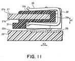
- Fig. 11 is a sectional view of the board- to-board connector according toa third embodiment of this invention, wherein the board-to-board connectorconnects two boards to each other.
- With reference to Figs. 3 through 7, description will be made about aboard-to-board connector according to a first embodiment of this invention.Similar parts are designated by like reference numerals.
- The board-to-board connector is for electrically connecting the first or
LCD board 21 to the second ormain board 22. Thefirst board 21 is of arectangular-shape. Thesecond board 22 is of a generally rectangular-shape. In the manner which will later be described, the first and thesecond boards - The board-to-board connector comprises an
insulator 31 placed in thespace S and a plurality ofconductive contacts 32 assembled to theinsulator 31and arranged at a predetermined interval in a second direction A2 perpendicularto the first direction A1. Each of thecontacts 32 Is formed to have aU-shapedportion 33 and a hairpin-shapedportion 34 which are coupled to each other. - More particularly, each of the
contacts 32 comprises abase portion 32a,a firstelastic portion 32b, afirst contact portion 32c, a secondelastic portion 32d,and asecond contact portion 32e. Thebase portion 32a is placed in the spaceS and held by theinsulator 31 and extends in a third direction A3 perpendicularto the first and the second directions A2 and A3. The firstelastic portion 32bextends from thebase portion 32a to face theprimary surface 21 a of thefirstboard 21. Thefirst contact portion 32c is protruded from the firstelastic portion 32b towards theprimary surface 21 a for coming in contact with one of thefirstelectrode patterns 25 by elastic force of the firstelastic portion 32b. Thesecondelastic portion 32d extends from thebase portion 32a between thebaseportion 32a and theprincipal surface 22a of thesecond board 22. Thesecondcontact portion 32e protrudes from the secondelastic portion 32d towards theprincipal surface 22a of thesecond board 22 for coming in contact with one ofthesecond electrode patterns 26 by elastic force of the secondelastic portion 32d. - Thus, the first and the
second boards first contact portion 32c is brought into contact withtheelectrode pattern 25 on thefirst board 21 by the elastic force of the firstelastic portion 32b, the connector can easily be released from thefirst board 21.Even if the distance or the space S between the first and thesecond board contact 32 has the elasticforce. - Each of the
contacts 32 further comprises an engagingportion 32fconnected to thefirst contact portion 32c. The engagingportion 32f has ashape adapted for engaging with aconnector inserting jig 41 in the first directionA1. More particularly, the engagingportion 32f is of a sickle-shape and isformed at an end of thefirst contact portion 32c of eachcontact 32. - Before the
first board 21 is inserted into theU-shaped portion 33, aprojecting portion 41 a of theconnector inserting jig 41 is engaged with theengagingportion 32f to widen theU-shaped portion 33 as shown in Fig. 7.Thus, thefirst board 21 is readily attached to theinsulator 31. In addition, theelectrode pattern 25 on thefirst board 21 is hardly damaged by thefirst contactportion 32c in eachcontact 32. - The board-to-board connector further comprises a pair of
clips 35 forclipping thefirst board 21 and theinsulator 31 in the first direction A1 to fix theinsulator 31 to thefirst board 21. It is preferable that an insulation coating suchas polyimide is provided at a part of eachclip 35 to be brought into contact withtheelectrode patterns 25 on thefirst board 21. In this event, it is possible toprevent short-circuiting of theelectrode patterns 25 on thefirst board 21 via theclips 35. - Referring to Figs. 8A through 9, the description will be directedconnection structure using the board-to-board connector.
- In order to connect the first and the
second boards member 36 and aframe 37.The fixingmember 36 is of a generally rectangular-shape and has ahole 36aformed at the center of each of the both side surfaces thereof and an engagingportions 36b formed at the four corners thereof for engaging with theframe 37 in the first direction A1. Theframe 37 is of a generally rectangular-shape andhas aprojection 37a formed at the center of each of the both side surfacesthereof. - The board-to-board connector is at first fixed to the
first board 21 by theclips 35. Next, thefirst board 21 is mounted on theframe 37 made of syntheticresin. In this event, the board-to-board connector is located in arecess 38 at afront side of theframe 37. Subsequently, theframe 37 is placed on thefirstboard 22. As a result, thefirst board 21, theframe 37, and thesecond board 22 are stacked. In this state, theframe 37 is interposed between the first andthesecond boards - Furthermore, the fixing
member 36 is mounted on thefirst board 21. Inthis event, thehole 36a of the fixingmember 36 is fitted to theprojection 37a oftheframe 37. Thehole 36a has a hole defining edge which will be referred toas a second engaging part. - Moreover, the engaging
portions 36b of the fixingmember 36 areinserted intorecesses 22c formed at two positions of the both sides of the .second board 22. In this state, ahook 36c formed on each engagingportion 36b is engaged with the lower surface of thesecond board 22 by the elasticity,as illustrated in Fig. 8C. Thehook 36c will be referred to as a first engagingpart. - Finally, the state illustrated in Fig. 9 is obtained. Specifically, the
firstcontact portion 32c of eachcontact 32 is brought Into contact with theelectrodepattern 25 on thefirst board 21 while thesecond contact portion 32e of eachcontact 32 is brought into contact with theelectrode pattern 26 on thesecondboard 22. Thus, the first and thesecond boards - With reference to Fig. 10, the description will be made as regards aboard-to-board connector according to a second embodiment of this invention. Similar parts are designated by like reference.
- In the board-to-board connector, the
insulator 31, the hairpin-shapedportion 34, a lower part of theU-shaped portion 33, and thesecond contactportion 32e are arranged between the first and thesecond boards first board 21 is supported by theinsulator 31 and the lower part of theU-shapedportion 33. However, it is possible to modify the design so that thefirstboard 21 is supported only by either one of them. - With reference to Fig. 11, the description will be made as regards aboard-to-board connector according to a third embodiment of this invention.Similar parts are designated by like reference.
- In the board-to-board connector, the
insulator 31 has aU-shapedportion 31 a which is elastically deformable in the first direction A1. Thefirstboard 21 is inserted into agroove 31 b of theU-shaped portion 31a. In otherwords, theU-shaped portion 31a is fitted over an end portion of thefirst board 21. In addition, theU-shaped portion 31a is clipped or pinched by theclips 35.Thus, thefirst board 21 is held by theinsulator 31.
Claims (7)
- A board-to-board connector for electrically connecting afirst and a second board (21, 22) to each other, said firstboard (21) having primary surface (21a) and a secondarysurface (21b) opposed to said primary surface (21a) in afirst direction (A1), said second board (22) having aprincipal surface (22a) facing said secondary surface (21b)with a space (S) left therebetween in said first direction(A1), said first board (21) having a plurality of firstelectrode patterns (25) arranged on said primary surface(21a), said second board (22) having a plurality of secondelectrode patterns (26) arranged on said principal surface(22a), said board-to-board connector comprising an insulator(31) and a plurality of conductive contacts (32) assembledto said insulator (31), each of said conductive contacts(32) comprising:characterized in that each of said conductive contacts (32)comprises an engaging portion (32f) extending from saidfirst elastic portion (32b), said engaging portion (32f)protruding from said first contactportion (32c), being the end portionof the contacts (32) and beingsubstantially parallel to the baseportion (32a) before insertion ofsaid first board (21), and being adapted for engaging with a connectorinserting jig (41) in said first direction (A1) for movingsaid first contact portion (32c) away from said insulator(31).a base portion (32a) placed in said space (S) and held bysaid insulator (31), said base portion (32a) extendingparallel to said first board (21);a first elastic portion (32b) extending from said baseportion (32a) to face said primary surface (21a), said firstelastic portion (32b) cooperating with said base portion(32a) to form a U-shaped portion (33) therebetween;a first contact portion (32c) protruding from said firstelastic portion (32b) towards said primary surface (21a) forcoming in contact with one of said first electrode patterns(25), by elastic force of said U-shaped portion (33);a second elastic portion (32d) extending from said baseportion (32a) between said base portion (32a) and saidprincipal surface (22a), said second elastic portion (32d)cooperating with said base portion (32a) to form a hairpin-shapedportion (34) therebetween; anda second contact portion (32e) protruding from said secondelastic portion (32d) towards said principal surface (22a)for coming in contact with one of said second electrodepatterns (26) by elastic force of said hairpin-shapedportion (34);
- A board-to-board connector as claimed in claim 1, wherein saidinsulator (31) is placed in said space (S), said board-to-board connector furthercomprising a clip (35) for clipping said first board (21) and said insulator (31) in said firstdirection (A1) to fix said insulator (31) to said first board (21).
- A board-to-board connector as claimed in claim 3, wherein said clip (35)is insulated from said first board (21).
- A board-to-board connector as claimed in one of claims 1 to 3, wherein saidinsulator (31) has a U-shaped portion fitted over an end portion of said first board (21),said U-shaped portion of said insulator (31) being elastically deformable in said first direction (A1), saidboard-to-board connector further comprising a clip (35) for clipping said U-shapedportion of said insulator (31) in said first direction (A1) to fix said insulator (31) to said first board (21).
- A board-to-board connector as claimed in one of claims 1 to 4, furthercomprising a frame (37) interposed between said first and said second boards (21,22) toform said space (S) and a fixing member (36) superposed on said first board (21) and havinga first engaging part (36c) for engaging with said second board (22) in said first direction (A1).
- A board-to-board connector as claimed as claim 5, wherein saidfixing member (36) further has a second engaging part (36a) for engaging with said frame (37)in said first direction (A1).
- A board-to-board connector as claimed in one of claims 1 to 6, wherein saidconductive contacts (32) are arranged in a second direction (A2) perpendicular to saidfirst direction (A1), said base portion (32a) extending in a third direction (A3) perpendicular tosaid first and said second directions (A1,A2).
Applications Claiming Priority (4)
| Application Number | Priority Date | Filing Date | Title |
|---|---|---|---|
| JP22140599 | 1999-08-04 | ||
| JP22140599 | 1999-08-04 | ||
| JP27839099AJP2001110488A (en) | 1999-08-04 | 1999-09-30 | Connector structure for connection between boards |
| JP27839099 | 1999-09-30 |
Publications (2)
| Publication Number | Publication Date |
|---|---|
| EP1075048A1 EP1075048A1 (en) | 2001-02-07 |
| EP1075048B1true EP1075048B1 (en) | 2002-11-27 |
Family
ID=26524275
Family Applications (1)
| Application Number | Title | Priority Date | Filing Date |
|---|---|---|---|
| EP00116800AExpired - LifetimeEP1075048B1 (en) | 1999-08-04 | 2000-08-03 | Board-to-board connector capable of readily electrically connecting two parallel boards to each other |
Country Status (10)
| Country | Link |
|---|---|
| US (1) | US6312263B1 (en) |
| EP (1) | EP1075048B1 (en) |
| JP (1) | JP2001110488A (en) |
| KR (1) | KR100384740B1 (en) |
| CN (1) | CN100369330C (en) |
| DE (1) | DE60000849T2 (en) |
| DK (1) | DK1075048T3 (en) |
| MY (1) | MY121161A (en) |
| SG (1) | SG93876A1 (en) |
| TW (1) | TW457751B (en) |
Families Citing this family (32)
| Publication number | Priority date | Publication date | Assignee | Title |
|---|---|---|---|---|
| AU3449700A (en)* | 1999-03-08 | 2000-09-28 | Whitaker Corporation, The | Board-mounted connector |
| US6468891B2 (en)* | 2000-02-24 | 2002-10-22 | Micron Technology, Inc. | Stereolithographically fabricated conductive elements, semiconductor device components and assemblies including such conductive elements, and methods |
| FR2814858B1 (en)* | 2000-10-02 | 2002-12-20 | Cit Alcatel | SPRING CONNECTOR FOR THE ELECTRICAL CONNECTION OF TRACKS OF A DISPLAY SCREEN WITH AN ELECTRICAL CIRCUIT |
| US6506059B2 (en)* | 2001-03-29 | 2003-01-14 | Avx Corporation | Electrical connectors for display devices |
| US6842333B2 (en)* | 2001-09-13 | 2005-01-11 | Lg Electronics, Inc. | Portable electronic device having LCD and touch screen |
| JP2003198161A (en)* | 2001-12-26 | 2003-07-11 | Mitsubishi Electric Corp | A clip-type lead and a main board on which a semiconductor device or a sub-board is mounted by the clip-type lead |
| US6913477B2 (en)* | 2002-03-01 | 2005-07-05 | Mobilewise, Inc. | Wirefree mobile device power supply method & system with free positioning |
| US7040902B2 (en)* | 2003-03-24 | 2006-05-09 | Che-Yu Li & Company, Llc | Electrical contact |
| US20050139995A1 (en)* | 2003-06-10 | 2005-06-30 | David Sarraf | CTE-matched heat pipe |
| US20050173098A1 (en)* | 2003-06-10 | 2005-08-11 | Connors Matthew J. | Three dimensional vapor chamber |
| WO2005017732A1 (en)* | 2003-08-18 | 2005-02-24 | Gunze Limited | Transparent touch panel and electronic apparatus |
| TWM259337U (en)* | 2003-11-21 | 2005-03-11 | Hon Hai Prec Ind Co Ltd | Electrical connector |
| JP4507789B2 (en) | 2004-09-21 | 2010-07-21 | 日本電気株式会社 | Stacking connector fixing structure, electronic equipment |
| US7297005B1 (en)* | 2006-06-27 | 2007-11-20 | Molex Incorporated | Connector pedestal |
| JP5763751B2 (en) | 2010-05-08 | 2015-08-12 | ザ、リージェンツ、オブ、ザ、ユニバーシティ、オブ、カリフォルニアThe Regents Of The University Of California | SEM scanner detection apparatus, system and method for early detection of ulcers |
| US8547699B1 (en) | 2010-11-09 | 2013-10-01 | Adtran, Inc. | Enclosure for outside plant equipment with interconnect for mating printed circuit boards, printed circuit board device and method of repairing outside plant equipment |
| DE102011114936B4 (en)* | 2011-10-06 | 2018-01-04 | Wago Verwaltungsgesellschaft Mbh | Electronic module and contact element for this purpose |
| JP6116056B2 (en)* | 2013-08-07 | 2017-04-19 | 日本航空電子工業株式会社 | connector |
| CA2982249C (en) | 2015-04-24 | 2019-12-31 | Bruin Biometrics, Llc | Apparatus and methods for determining damaged tissue using sub-epidermal moisture measurements |
| KR101689470B1 (en)* | 2015-06-12 | 2016-12-23 | 김동욱 | Hood filter for gas range |
| DE102015212163B4 (en)* | 2015-06-30 | 2024-05-29 | Robert Bosch Gmbh | Contact spring for a display device, display device and method for producing a display device |
| CN106410517B (en)* | 2015-07-29 | 2019-04-26 | 富士康(昆山)电脑接插件有限公司 | Electric connector and combinations thereof |
| GB2545425B (en)* | 2015-12-14 | 2019-03-27 | Ge Aviat Systems Ltd | Distributed wiring board connections |
| ES2966366T3 (en) | 2017-02-03 | 2024-04-22 | Bbi Medical Innovations Llc | Tissue viability measurement |
| KR102694209B1 (en) | 2017-02-03 | 2024-08-13 | 브루인 바이오메트릭스, 엘엘씨 | Measurement of edema |
| GB2591707B (en) | 2017-02-03 | 2021-11-17 | Bruin Biometrics Llc | Measurement of susceptibility to diabetic foot ulcers |
| AU2018368707B2 (en) | 2017-11-16 | 2024-03-07 | Bruin Biometrics, Llc | Strategic treatment of pressure ulcer using sub-epidermal moisture values |
| US10698274B2 (en) | 2017-12-22 | 2020-06-30 | Sakai Display Products Corporation | Display apparatus and method for manufacturing display apparatus |
| AU2019217995B2 (en) | 2018-02-09 | 2024-11-14 | Bruin Biometrics, Llc | Detection of tissue damage |
| PL3861601T3 (en)* | 2018-10-11 | 2024-06-10 | Bruin Biometrics, Llc | DEVICE WITH A SINGLE-USE ELEMENT |
| US11594834B2 (en)* | 2020-04-30 | 2023-02-28 | Lear Corporation | Electrical connector assembly |
| MX2023009108A (en) | 2021-02-03 | 2023-08-09 | Bruin Biometrics Llc | Methods of treating deep and early-stage pressure induced tissue damage. |
Family Cites Families (12)
| Publication number | Priority date | Publication date | Assignee | Title |
|---|---|---|---|---|
| US3598960A (en)* | 1969-07-03 | 1971-08-10 | George P Deacon | Radiant ceiling heating unit |
| FR2475809A1 (en) | 1980-02-07 | 1981-08-14 | Socapex | CONNECTOR BAR FOR CONNECTOR CARD, AND CONNECTOR PROVIDED WITH SUCH BARRETTES |
| US4530554A (en) | 1983-12-27 | 1985-07-23 | Northern Telecom Limited | High density low profile multiple contact connector |
| US4769908A (en)* | 1985-11-04 | 1988-09-13 | Amp Incorporated | Method of manufacturing a plurality of contact terminals |
| US4738625A (en) | 1986-09-29 | 1988-04-19 | Bell Telephone Laboratories, Inc. | Electrical connectors for circuit panels |
| JPH0638353B2 (en) | 1988-07-18 | 1994-05-18 | ヒロセ電機株式会社 | Socket for electronic parts |
| US5561322A (en)* | 1994-11-09 | 1996-10-01 | International Business Machines Corporation | Semiconductor chip package with enhanced thermal conductivity |
| US5906496A (en)* | 1996-12-23 | 1999-05-25 | Thomas & Betts International, Inc. | Miniature card edge clip |
| US5888076A (en) | 1997-06-13 | 1999-03-30 | Japan Aviation Elecronics Industry, Limited | LCD panel connector for use in connection between an LCD panel and a circuit board |
| US6091474A (en)* | 1997-06-26 | 2000-07-18 | Ericsson, Inc. | Display assembly |
| US6089876A (en)* | 1997-08-15 | 2000-07-18 | Japan Aviation Electronics Industry, Limited | Clip connector |
| US6151219A (en)* | 1999-02-01 | 2000-11-21 | Itt Manufacturing Enterprises, Inc. | Electronic card with sheet metal and overmolded plastic frame parts |
- 1999
- 1999-09-30JPJP27839099Apatent/JP2001110488A/enactivePending
- 2000
- 2000-07-31USUS09/629,014patent/US6312263B1/ennot_activeExpired - Fee Related
- 2000-07-31CNCNB001211927Apatent/CN100369330C/ennot_activeExpired - Fee Related
- 2000-08-02MYMYPI20003530Apatent/MY121161A/enunknown
- 2000-08-02TWTW089115482Apatent/TW457751B/ennot_activeIP Right Cessation
- 2000-08-03EPEP00116800Apatent/EP1075048B1/ennot_activeExpired - Lifetime
- 2000-08-03DEDE60000849Tpatent/DE60000849T2/ennot_activeExpired - Fee Related
- 2000-08-03DKDK00116800Tpatent/DK1075048T3/enactive
- 2000-08-03SGSG200004353Apatent/SG93876A1/enunknown
- 2000-08-04KRKR10-2000-0045237Apatent/KR100384740B1/ennot_activeExpired - Fee Related
Also Published As
| Publication number | Publication date |
|---|---|
| SG93876A1 (en) | 2003-01-21 |
| US6312263B1 (en) | 2001-11-06 |
| CN100369330C (en) | 2008-02-13 |
| KR100384740B1 (en) | 2003-05-22 |
| DK1075048T3 (en) | 2003-03-24 |
| CN1283883A (en) | 2001-02-14 |
| EP1075048A1 (en) | 2001-02-07 |
| KR20010067058A (en) | 2001-07-12 |
| TW457751B (en) | 2001-10-01 |
| MY121161A (en) | 2005-12-30 |
| DE60000849T2 (en) | 2003-07-03 |
| JP2001110488A (en) | 2001-04-20 |
| DE60000849D1 (en) | 2003-01-09 |
Similar Documents
| Publication | Publication Date | Title |
|---|---|---|
| EP1075048B1 (en) | Board-to-board connector capable of readily electrically connecting two parallel boards to each other | |
| US7303403B2 (en) | Electrical connecting member capable of achieving stable connection with a simple structure and connector using the same | |
| CN108736192B (en) | Electrical connector | |
| KR0122783Y1 (en) | Edge connector for printed circuit boards | |
| US5702269A (en) | Electrical connector | |
| KR101053753B1 (en) | connector | |
| US20030211783A1 (en) | Connector which can be simplified in structure of an end portion in a card inserting/removing direction | |
| KR100567587B1 (en) | Electrical connector having a holddown for ground connection | |
| JPH06325825A (en) | Connector device | |
| US7153144B2 (en) | Module connector | |
| JP2000251971A (en) | Electric connector for antenna | |
| JP2004296419A (en) | Connector | |
| JP4270451B2 (en) | connector | |
| JPH03133070A (en) | Electronic components for surface mounting | |
| JP3549851B2 (en) | connector | |
| US8591263B2 (en) | Connector for connecting cable and terminal of same | |
| JPH075262U (en) | Board connection shock absorption connector device | |
| KR20040060773A (en) | Connector | |
| JP2000244148A (en) | Electronic component connector and board connector | |
| JP3443864B2 (en) | Stacking connector | |
| JP2603084Y2 (en) | connector | |
| JP2002042925A (en) | Board connector | |
| JPH08116148A (en) | Connection structure of circuit board and fpc | |
| JP2557420Y2 (en) | Circuit board connector | |
| JP2001143795A (en) | Connector for fpc/ffc without soldering |
Legal Events
| Date | Code | Title | Description |
|---|---|---|---|
| PUAI | Public reference made under article 153(3) epc to a published international application that has entered the european phase | Free format text:ORIGINAL CODE: 0009012 | |
| AK | Designated contracting states | Kind code of ref document:A1 Designated state(s):DE DK FI FR GB SE | |
| AX | Request for extension of the european patent | Free format text:AL;LT;LV;MK;RO;SI | |
| 17P | Request for examination filed | Effective date:20010514 | |
| 17Q | First examination report despatched | Effective date:20010705 | |
| AKX | Designation fees paid | Free format text:DE DK FI FR GB SE | |
| GRAG | Despatch of communication of intention to grant | Free format text:ORIGINAL CODE: EPIDOS AGRA | |
| GRAG | Despatch of communication of intention to grant | Free format text:ORIGINAL CODE: EPIDOS AGRA | |
| GRAH | Despatch of communication of intention to grant a patent | Free format text:ORIGINAL CODE: EPIDOS IGRA | |
| GRAH | Despatch of communication of intention to grant a patent | Free format text:ORIGINAL CODE: EPIDOS IGRA | |
| GRAA | (expected) grant | Free format text:ORIGINAL CODE: 0009210 | |
| AK | Designated contracting states | Kind code of ref document:B1 Designated state(s):DE DK FI FR GB SE | |
| REG | Reference to a national code | Ref country code:GB Ref legal event code:FG4D | |
| REF | Corresponds to: | Ref document number:60000849 Country of ref document:DE Date of ref document:20030109 | |
| REG | Reference to a national code | Ref country code:DK Ref legal event code:T3 | |
| ET | Fr: translation filed | ||
| PLBE | No opposition filed within time limit | Free format text:ORIGINAL CODE: 0009261 | |
| STAA | Information on the status of an ep patent application or granted ep patent | Free format text:STATUS: NO OPPOSITION FILED WITHIN TIME LIMIT | |
| 26N | No opposition filed | Effective date:20030828 | |
| PGFP | Annual fee paid to national office [announced via postgrant information from national office to epo] | Ref country code:DK Payment date:20070713 Year of fee payment:8 | |
| PGFP | Annual fee paid to national office [announced via postgrant information from national office to epo] | Ref country code:DE Payment date:20070822 Year of fee payment:8 | |
| PGFP | Annual fee paid to national office [announced via postgrant information from national office to epo] | Ref country code:FI Payment date:20070807 Year of fee payment:8 | |
| PGFP | Annual fee paid to national office [announced via postgrant information from national office to epo] | Ref country code:GB Payment date:20070731 Year of fee payment:8 | |
| PGFP | Annual fee paid to national office [announced via postgrant information from national office to epo] | Ref country code:SE Payment date:20070808 Year of fee payment:8 | |
| PGFP | Annual fee paid to national office [announced via postgrant information from national office to epo] | Ref country code:FR Payment date:20070830 Year of fee payment:8 | |
| REG | Reference to a national code | Ref country code:DK Ref legal event code:EBP | |
| EUG | Se: european patent has lapsed | ||
| GBPC | Gb: european patent ceased through non-payment of renewal fee | Effective date:20080803 | |
| PG25 | Lapsed in a contracting state [announced via postgrant information from national office to epo] | Ref country code:FI Free format text:LAPSE BECAUSE OF NON-PAYMENT OF DUE FEES Effective date:20080803 | |
| REG | Reference to a national code | Ref country code:FR Ref legal event code:ST Effective date:20090430 | |
| PG25 | Lapsed in a contracting state [announced via postgrant information from national office to epo] | Ref country code:DK Free format text:LAPSE BECAUSE OF NON-PAYMENT OF DUE FEES Effective date:20080831 | |
| PG25 | Lapsed in a contracting state [announced via postgrant information from national office to epo] | Ref country code:DE Free format text:LAPSE BECAUSE OF NON-PAYMENT OF DUE FEES Effective date:20090303 Ref country code:FR Free format text:LAPSE BECAUSE OF NON-PAYMENT OF DUE FEES Effective date:20080901 | |
| PG25 | Lapsed in a contracting state [announced via postgrant information from national office to epo] | Ref country code:GB Free format text:LAPSE BECAUSE OF NON-PAYMENT OF DUE FEES Effective date:20080803 | |
| PG25 | Lapsed in a contracting state [announced via postgrant information from national office to epo] | Ref country code:SE Free format text:LAPSE BECAUSE OF NON-PAYMENT OF DUE FEES Effective date:20080804 |