EP1074995A1 - Method for programming multi-level non-volatile memories by controlling the gate voltage - Google Patents
Method for programming multi-level non-volatile memories by controlling the gate voltageDownload PDFInfo
- Publication number
- EP1074995A1 EP1074995A1EP99830501AEP99830501AEP1074995A1EP 1074995 A1EP1074995 A1EP 1074995A1EP 99830501 AEP99830501 AEP 99830501AEP 99830501 AEP99830501 AEP 99830501AEP 1074995 A1EP1074995 A1EP 1074995A1
- Authority
- EP
- European Patent Office
- Prior art keywords
- programming
- level
- pulses
- programmed
- verify
- Prior art date
- Legal status (The legal status is an assumption and is not a legal conclusion. Google has not performed a legal analysis and makes no representation as to the accuracy of the status listed.)
- Granted
Links
- 238000000034methodMethods0.000titleclaimsdescription36
- 230000015654memoryEffects0.000titleclaimsdescription24
- 239000000243solutionSubstances0.000description6
- 230000003111delayed effectEffects0.000description5
- AHLBNYSZXLDEJQ-FWEHEUNISA-NorlistatChemical compoundCCCCCCCCCCC[C@H](OC(=O)[C@H](CC(C)C)NC=O)C[C@@H]1OC(=O)[C@H]1CCCCCCAHLBNYSZXLDEJQ-FWEHEUNISA-N0.000description5
- 238000010586diagramMethods0.000description4
- 230000008901benefitEffects0.000description3
- 230000009467reductionEffects0.000description3
- 230000006399behaviorEffects0.000description2
- 230000004048modificationEffects0.000description2
- 238000012986modificationMethods0.000description2
- 230000001052transient effectEffects0.000description2
- 241000220010RhodeSpecies0.000description1
- 230000003213activating effectEffects0.000description1
- 230000004913activationEffects0.000description1
- 238000013500data storageMethods0.000description1
- 230000000593degrading effectEffects0.000description1
- 238000009826distributionMethods0.000description1
- 230000000694effectsEffects0.000description1
- 238000005516engineering processMethods0.000description1
- 230000007613environmental effectEffects0.000description1
- 230000006870functionEffects0.000description1
- 230000006872improvementEffects0.000description1
- 238000002347injectionMethods0.000description1
- 239000007924injectionSubstances0.000description1
- 230000002045lasting effectEffects0.000description1
- 238000004519manufacturing processMethods0.000description1
- 230000001151other effectEffects0.000description1
- 230000008569processEffects0.000description1
- 239000004065semiconductorSubstances0.000description1
- 238000000926separation methodMethods0.000description1
- 230000001360synchronised effectEffects0.000description1
Images


Classifications
- G—PHYSICS
- G11—INFORMATION STORAGE
- G11C—STATIC STORES
- G11C11/00—Digital stores characterised by the use of particular electric or magnetic storage elements; Storage elements therefor
- G11C11/56—Digital stores characterised by the use of particular electric or magnetic storage elements; Storage elements therefor using storage elements with more than two stable states represented by steps, e.g. of voltage, current, phase, frequency
- G11C11/5621—Digital stores characterised by the use of particular electric or magnetic storage elements; Storage elements therefor using storage elements with more than two stable states represented by steps, e.g. of voltage, current, phase, frequency using charge storage in a floating gate
- G11C11/5628—Programming or writing circuits; Data input circuits
Definitions
- the present inventionrelates a method for programming multi-level non-volatile memories by controlling the gate voltage.
- the inventionspecifically refers to non-volatile memories formed of floating gate cells (EPROM, EEPROM, flash) in which the cells programming is performed by modifying the threshold voltage of the cells, that is modifying the amount of the charge stored in the floating gate region.
- EPROMfloating gate cells
- EEPROMelectrically erasable programmable read-only memory
- flashfloating gate cells
- the present methodhowever can be applied also to memory cells of a different type (for example MNOS, i.e. Metal-Nitride-Oxide-Semiconductor technology cells).
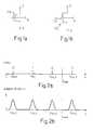
- Figure 1shows the electric diagram of a typical floating gate memory cell having a drain terminal D, a source terminal S, a control gate terminal (herein below also defined gate terminal) CG and a body terminal B.
- Figure 1further shows the floating gate region FG.
- Figure 2shows the symbol of a different memory cell, the so called "split-gate".
- the programmable threshold levelsmust be placed to a certain mutual distance, in order to be able to be recognized without errors when read. Moreover, the threshold voltage cannot be programmed exactly at the desired value: every level corresponds in practice to certain threshold voltage interval, as shown by the comparison between Figure 2a and Figure 2b related to four-level programmable cells.
- Figure 2ashows the ideal case in which it is supposed to obtain a precise programming of each of four threshold voltage levels, while Figure 2b shows a more realistic case, in which every logic value corresponds to a certain threshold voltage interval.
- Figure 2aalso shows the correspondence assigned, as an exemplificative but non limiting example, between the different threshold voltage values and programmed levels (respectively 0, 1, 2 and 3).
- the threshold voltage interval corresponding to each programmable levelmust be sufficiently reduced so that the intervals corresponding to adjacent levels can be placed at such a mutual distance as to guarantee safe maintaining and recognizing of data stored into the cells, without having to use a global interval excessively wide to allocate all desired logic levels. In fact, there are both a lower limit and an upper limit for this global interval, dictated by practical reasons and reliability reasons. In order to compute the optimum distance between threshold voltage intervals corresponding to different stored levels, effects such as reading and programming circuits inaccuracy and environmental conditions variations, degrading time of the stored charge and reading and programming noises must also be taken into account, since they create an undesired stored charge variation, as known to the skilled person.
- the multi-level cell programmingis performed through the technique defined as "program and verify”.
- a programming operationis performed through a succession of programming pulses and, after having applied each programming pulse, it is verified whether the programmed cell threshold voltages reached the respective desired value, as schematically shown in Figure 3: if a certain cell has reached the desired threshold level, it does not receive any further programming pulses.
- Verifyingis usually performed simultaneously for all cells in a group of cells (one or more words) that are programmed in parallel and for any desired programming level, it consists in comparing, directly or indirectly, a cell threshold voltage with preset reference values V ref,i . Programming and verifying continue until all cells in a group have been programmed at the respective desired level.
- Relationship (1)is valid for any cell, but the relationship between the voltage value applied to the cell gate terminal during the last programming pulse, and the threshold voltage value V TH reached by the cell at the end of such pulse cannot be determined a priori for a specific cell.
- relationship (1)shows the threshold voltage increase upon every programming pulse, but not its absolute value.
- Such absolute valuein fact depends on different factors linked to the manufacturing process (for programmable cells through hot channel electron injection, for example, it depends firstly on the effective cell channel length).
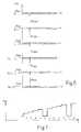
- FIG 4shows the behavior of the threshold voltage Vth obtained by representing along the ordinate the threshold voltage after applying each programming pulse N (shown along the abscissa) and connecting the points thereby obtained, for three different cells (in particular, curves A, B, and C refer to cells having respectively increasing channel lengths).
- the threshold voltageincreases linearly, with increments ⁇ V GP upon every programming pulse, along three mutually parallel straight lines.
- relationship (1)it is not possible to know on which of the three straight lines the threshold voltage of a specific cell is moving during programming and therefore is not possible to compute the absolute threshold voltage value Vth reached after each pulse.
- the memory cellsare programmed by applying programming pulses with a constant length, constant drain voltage, and progressively increasing gate voltage with a constant increase equal to ⁇ V GP between two subsequent pulses. Therefore the gate terminal voltage plot as shown in Figure 5 is obtained. Under ideal conditions, with this technique the width of the intervals corresponding to programmed levels (hereinbelow called program level width) is equal to ⁇ V GP .
- the ( j-1) -th programming pulsepreceding the one in which the threshold voltage corresponding to the desired programming level ( i -th level) is reached and whose comparison reference level during verifying is equal to V ref,i , determines a threshold voltage that is less than V ref,i but next to this one, while when j -th programming pulse is provided, the threshold voltage goes to a value equal to the previous value plus ⁇ V GP , so that it will not be greater than V ref,i , + ⁇ V GP .
- the threshold voltage for the program cells at level V TH,iexceeds the reference value V ref,i , by an amount included between 0 and ⁇ V GP .
- the reduction in the increase ⁇ V GPrequires a corresponding increase of the number of programming and verifying pulses necessary to reach a preset final threshold voltage starting from a predetermined initial value.
- the increase of the number of programming and verifying pulsesgenerates an increase of the global time necessary to program a memory cell at a preset threshold level.
- the time necessary for a complete programming and verifying stepis decisely greater than the time for a single programming pulse, above all in the case of short time programming pulses (1 ⁇ s or less).
- it is necessary to deactivate the programming circuitryactivate the reading circuitry inside the integrated circuit and wait for the reading voltages to be applied to cells to reach the desired value with a sufficient accuracy, which requires a certain length of time.
- the accuracy required for bias voltagesincreases along with a decrease in the distance between threshold voltages corresponding to adjacent programmed levels (the cell current when reading, and, therefore, when verifying strictly depends on the value of voltages applied to drain and gate terminals).
- T GP(1+ ⁇ )
- T GPis the length of a programming pulse and ⁇ is greater than 0 and generally can be of the order of one.
- Aim of the inventionis thereby providing a programming method that minimizes the global time necessary for a complete programming operation with the same number of programming pulses, allowing an improvement in the compromise between accuracy and global programming time.
- the interval between nominal values of two following levelsis divided into a plurality of intervals whose width is equal to the gate voltage increase applied during programming, plus eventually a interval whose width is less than the increase. It is not mandatory that the interval between levels is constant or that it is an exact integer multiple of applied gate voltage increments ⁇ V GP .
- Programmingis then performed by applying a plurality of programming pulses equal to the plurality of preset increments, without performing intermediate verify steps and the reached threshold voltage verify is performed only after the plurality of programming steps have been performed, when the reached threshold voltage is presumably equal or slightly greater than the minimum desired threshold voltage for the considered level for at least one of the cells being programmed. To be prudent, verifying can be carried out after the programming pulse that, presumably, is immediately preceding the desired threshold voltage being reached, corresponding to the provided programming level.
- the programmed levels configuration and the increment value ⁇ V GPare such that the level widening due to the increment with ⁇ V GP is much less than the distance between nominal values of the levels. For example to go from a programming level to another, 7 programming steps are performed.
- Such configurationis advantageously used in case of memories with many programmable levels per cell, in which a high programmed level accuracy is desired in order to allocate adequate separation gaps between adjacent programmable levels to take into account the existing uncertainty conditions.
- V m,11 V
- V m,22 V
- V m,33 V
- N-1 programming pulsesare applied with an increasing gate voltage, with increment ⁇ V GP , without carrying out any verify after each pulse; in this way one is sure that the cell cannot still have reached the level ( i+1 )-th.
- a further pulse (N-th)is applied with a gate voltage increment ⁇ V GP , and verify is performed. If the threshold voltage has not yet been reached, a further pulse (( N + 1)-th) is applied with a still increased gate voltage by the provided increase, eventually followed by a further verify step, even if this one is not strictly necessary, since the threshold voltage now must have already reached level ( i+1 )-th.
- Figure 7shows the plot of the gate voltage during programming of a cell according to the invention, supposing that N is equal to 4 and that the verify step immediately provides positive result.
- Figure 7must be compared with Figure 5 and shows how, with the invention, it is possible to apply a greater number of programming impulses with a same global time.
- the known solutionrequires a timing equal to N(1+ ⁇ )T GP while the present solution requires a time equal to (N+ ⁇ )T GP , with a time saving equal to (N-1) ⁇ T GP .
- N+1 programming stepsare necessary, the necessary time will be equal to (N+1+2 ⁇ )T GP or (N+1+ ⁇ )T GP depending on whether the last programming step for each level is followed, or not, by a verify step, with time saving respectively equal to (N-1) ⁇ T GP or N ⁇ T GP .
- a cell threshold voltagemust be taken from a generic level i to a level i+j , with j >1, it is possible both to program the cell every time to the following level i+1, i+2, ... until level i+j is reached by verifying every time that the single intermediate levels are reached, or to apply Z-1 pulses, where Z is the integer number obtained by truncating number j(N+ ⁇ ), then perform a complete programming and verify step, and if the cell has not yet reached the desired level, apply a last programming pulse (with or without final verify similarly to what has been previously stated).
- programming pulsesare simultaneously applied in the above described way to the cells that must be programmed at a different level from the minimum threshold level.
- a cellWhen a cell has reached the desired programming level, it does not receive any more programming pulses (such interruption is obtained in a known way: for example the related bit line, connected to the drain terminal is not biased any more at the programming voltage), and programming goes on for the other cells, until they are all programmed at the provided level. Obviously, no programming pulses are ever applied to the cells that must remain in the erased state.
- the cells that must be programmedare supplied with a set of programming pulses each followed by a verify step, until the threshold voltage of at least one of the cells reaches the value corresponding to the first level.
- a number A 1 of programming pulsesis then supplied, each followed by a verify step, until all cells to be programmed have a threshold voltage corresponding to level "1" (A 1 cannot be determined a priori).
- the cells that must be programmed at level "1"do not receive programming pulses after their threshold voltage has reached the desired value.
- N-(1+A 1 )N-1-A 1 pulses without verify (no cell, in fact, is programmed at level 2 after these pulses). Then further pulses are provided, each one followed by a verify step, until the threshold voltage of at least one cell reaches the second level, after which other A 2 programming pulses are provided followed by verify, until the threshold voltage of all the cells to be programmed at least at a second level has reached the desired value.
- the procedureis repeated, so that, to reach level i+1, N-A i -1 programming pulses are applied each time without verify, followed by an adequate number of programming pulses with verify until at least one cell has reached level (i+1)-th, and by A i + 1 pulses with verify, until all cells to be programmed at least to level i+1 have reached this level, and going on until all cells have been programmed at the provided level.
- N-1-A i verify stepsare saved for each level. Consequently, globally, the saved time is equal to:
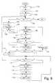
- a verify stepis performed, block 100; then a level counter i , associated with the level to be programmed, is set to zero (block 101), together with a pulse counter K, relative to programming pulses (block 102).
- block 106B i (number of pulses to be consecutively applied) is set equal to N i .
- Figure 9shows a variation of the flow-chart of Figure 8, in which no verify of intermediate levels for which there are no cells to be programmed, is carried out.
- block 105the number of pulses N i and the truncation ⁇ i are detected, obtained according to (2) for the i -th level.
- a number C iis computed that is equal to the ratio between ⁇ V DIST,I and ⁇ V GP for the i -th level, by adding N i and ⁇ i .
- a further global time savingcan be obtained if the minimum number D of pulses necessary to take an erased cell (state 0) to the lower end of the first programming level (state 1) is known a priori. This number can be computed for every die during the Electrical Wafer Sort. In such a case, when programming begins, D pulses without verify steps are initially applied to the cells that must be programmed, and then pulses with verify are applied until at least one of the cells reaches level "1". Programming then proceeds as previously described. '
- Figure 10shows a block diagram of a hardware circuit implementing the method in Figure 8.
- the circuitis timed by a signal CLOCK and by a signal CLOCK' delayed with respect to CLOCK .
- a programming operationis activated upon receiving a Program Start pulse (PR_ST), synchronous with CLOCK, that sets two flip-flops 1 and 2 taking signal PR_MODE ("Program mode”) and signal P&V (“Program&verify) to a high state.
- PR_STProgram Start pulse
- PR_MODEProgram Mode
- P&VProgram&verify
- the alternate setting of a verify step and a programming stepis ensured by the output switching of a delayed flip-flop 3 that switches at every pulse CLOCK if the signal P&V provided to the control input C of multiplexer 4 is at high level, since in this case the input D of the delayed flip-flop 3 receives the signal Q 3 of the delayed flip-flow 3.
- the output Q3 of the delayed flip-flop 3is set to 1 by signal PR_ST in order to perform a verify step.
- a high level on output Q3activates the "verify” (signal VR), while a low level activates the "program” signal PRG.
- Activation of signal VR or signal PRGallows (block 5) generating suitable signals to be sent to the memory array to respectively perform verify and programming operations, in a per se known manner.
- Generator 5receives at the input also signal CLOCK' (used for timing the signals to be sent to the memory array) in addition to-the value of the number of programming steps P already performed during the current programming cycle, to set the correct threshold voltage value according to an increasing law, as above described.
- the value of the global programming steps Pis generated by a first counter 6 reset by signal PR_ST at the beginning of a new programming operation.
- Signal P&Vdetermines if the circuit must perform a verify step after a programming step. In fact, if P&V has a high value, as stated above, output Q3 switches upon every CLOCK pulse alternatively activating signals VER and signal PROG; viceversa, if P&V has value 0, input D of delay flip-flop 3 coincides with output Q3 and does not switch. Consequently, the circuit is kept under "program" status.
- the control signal of multiplexer 4is generated as follows.
- the flip-flop 2is set and its output is high.
- a pulseis generated on signal "ONEi" (as described with reference to block 111 in Figures 8 and 9) and the contents of a second counter 7, storing the value of step counter k , are reset.
- the second counter 7is increased by one unit upon every programming pulse and is compared by a digital comparator 8 receiving the comparison value B i (number of programming pulses to be consecutively applied) by register 9.
- a third counter 10counts the number of levels so far programmed and then provides at the output the value of i .
- the third counter 10is initialised at state 1 at the beginning of a programming operation by signal PR_ST and has an output connected to a logic block 11 that provides register 9 with value B i depending on i .
- Loading of B iis performed at the beginning of the programming cycle related to the i -th level, when the previous cycle ends, as signaled by a pulse on signal ALLi causing the increase of the third counter 10 and the generation of a new value of B i .
- loading of B i in register 9is obtained through PR_ST.
- Block DELgenerates a suitable delay in the loading signal.
- Flip-flop 1is reset when the circuit is turned on (signal POR) and at the end of a whole programming operation, when signal PR_END switches to high state, causing switching of signal PR_MODE to 0, indicative of the circuit state, no more being programmed.
- the present methodallows on one hand to have the desired programming accuracy by setting a threshold voltage increase with a suitable value, and on the other hand to avoid that the global programming time is made excessively long, since verifying is performed when at least one cell has reached the desired threshold level.
- the present methodis particularly advantageously with a high number of levels to be programmed (for example from 16 on).
- a further reduction in the programming timesis obtained according to the described solutions, according to which verifying is avoided at intermediate levels at which no cells have to be programmed and, for each die, the number of pulses is stored necessary to reach the condition in which linear relationship (1) is valid at the beginning of a global programming operation.
Landscapes
- Engineering & Computer Science (AREA)
- Computer Hardware Design (AREA)
- Read Only Memory (AREA)
Abstract
Description

Claims (12)
- A method for programming non-volatile memory cells havinga gate terminal (CG), comprising the step of applying a set ofprogramming pulses, wherein, upon every programming pulse,said gate terminal is supplied with a gate voltage whose valueis increased with respect to the previous programming pulse,characterized by cyclically applying a plurality (Bi) ofconsecutive programming pulses without verify followed by averify step.
- The method according to claim 1, characterized in thatsaid plurality of pulses is equal to the nominal number ofpulses (N) necessary to take said cell from a currentprogramming level to a following programming level.
- The method according to claim 1 or 2, characterized inthat, upon every programming pulse, said gate voltage shows aconstant increase (ΔVGP) with respect to a previous programmingpulse.
- The method according to claim 3, characterized in thatbetween a current programming pulse and a followingprogramming pulse a threshold voltage difference (ΔVDIST) ispresent, equal to a multiple (Ci), also not integer, of saidconstant increment, and in that said plurality (B1) ofprogramming pulses is equal to an integer value obtained bytruncating said multiple.
- The method according to claim 4, characterized bydifferent threshold voltage steps between pairs of adjacentprogramming levels.
- The method according to any one of the previous claims,characterized by a first programming step starting from anerased state at a first programming level; said first programming step comprising a plurality of steps eachincluding a programming step and a verify step.
- The method according to any one of the previous claims,characterized by the step of programming a plurality of memorycells in parallel.
- The method according to any one of the previous claims,characterized by a cycle of steps comprising:detecting (105; 105') a first nominal number (Ni; Ci) ofprogramming pulses included between a current programminglevel and a following programming level;calculating (106; 106', 132-135) a number (Bi) ofprogramming pulses to be applied on the bias of said firstnominal number of programming pulsessupplying (108) said number of programming pulses to beapplied, without verify;performing ( 110 ) a verify step;repeating the steps of providing a programming pulse andperforming a verify step until at least one cell has reachedthe desired threshold value; andrepeating the steps of applying a programming step andperforming a verify step until all cells have reached adesired threshold level.
- The method according to claim 8, characterized byrepeating said cycle of steps until a maximum programminglevel.
- The method according to claim 8 or 9, characterized inthat said number (Bi) of programming pulses to be applied isequal to said first nominal number (Ni) of programming pulses.
- The method according to any one of claims 8-10,characterized in that said step of repeating further comprisesthe step of stopping (115) supplying the programming pulses to those cells to be programmed at said following programminglevel that have already reached said desired threshold value.
- The method according to claim 8, characterized in thatsaid step of calculating comprises the steps of:checking (132) whether there are cells to be programmed atsaid following programming level;if so, setting (106') said number (Bi) of programming pulsesto be applied equal to an integer value obtained by truncatingsaid first nominal number (Ci) of programming pulses;if not, increasing (133) a current level index, calculating(134) a second nominal number (Ci) of programming pulsesincluded between said current programming level and aprogramming level subsequent to said current programminglevel; summing (135) said first and second nominal numbers ofprogramming pulses; and repeating said steps of verifyingwhether there are cells to be programmed at said followingprogramming level, increasing a current level index, computinga second nominal number of programming pulses and summinguntil it is verified that there is at least one cell to beprogrammed at said following programming level; finally,setting (106') said number (Bi) of programming pulses to beapplied equal to an integer value obtained by truncating saidsecond nominal number (Ci) of programming pulses.
Priority Applications (4)
| Application Number | Priority Date | Filing Date | Title |
|---|---|---|---|
| DE69927967TDE69927967T2 (en) | 1999-08-03 | 1999-08-03 | Programming method of a non-volatile multi-bit memory by regulating the gate voltage |
| EP99830501AEP1074995B1 (en) | 1999-08-03 | 1999-08-03 | Method for programming multi-level non-volatile memories by controlling the gate voltage |
| US09/631,187US6366496B1 (en) | 1999-08-03 | 2000-08-02 | Method for programming multi-level non-volatile memories by controlling the gate voltage |
| JP2000236205AJP4469475B2 (en) | 1999-08-03 | 2000-08-03 | Programming method of multi-level non-volatile memory by controlling gate voltage |
Applications Claiming Priority (1)
| Application Number | Priority Date | Filing Date | Title |
|---|---|---|---|
| EP99830501AEP1074995B1 (en) | 1999-08-03 | 1999-08-03 | Method for programming multi-level non-volatile memories by controlling the gate voltage |
Publications (2)
| Publication Number | Publication Date |
|---|---|
| EP1074995A1true EP1074995A1 (en) | 2001-02-07 |
| EP1074995B1 EP1074995B1 (en) | 2005-10-26 |
Family
ID=8243537
Family Applications (1)
| Application Number | Title | Priority Date | Filing Date |
|---|---|---|---|
| EP99830501AExpired - LifetimeEP1074995B1 (en) | 1999-08-03 | 1999-08-03 | Method for programming multi-level non-volatile memories by controlling the gate voltage |
Country Status (4)
| Country | Link |
|---|---|
| US (1) | US6366496B1 (en) |
| EP (1) | EP1074995B1 (en) |
| JP (1) | JP4469475B2 (en) |
| DE (1) | DE69927967T2 (en) |
Cited By (5)
| Publication number | Priority date | Publication date | Assignee | Title |
|---|---|---|---|---|
| WO2003058637A1 (en)* | 2002-01-03 | 2003-07-17 | Intel Corporation | Programming non-volatile memory devices |
| SG105590A1 (en)* | 2002-10-07 | 2004-08-27 | Infineon Technologies Ag | Single bit nonvolatile memory cell and methods for programming and erasing thereof |
| CN100409367C (en)* | 2002-01-30 | 2008-08-06 | 旺宏电子股份有限公司 | Writing and clearing method for multi-value flash memory |
| WO2011127195A1 (en)* | 2010-04-09 | 2011-10-13 | Sandisk Corporation | Saw-shaped multi-pulse programming for program noise reduction in memory |
| US8045378B2 (en) | 2008-06-12 | 2011-10-25 | Sandisk Technologies Inc. | Nonvolatile memory with correlated multiple pass programming |
Families Citing this family (95)
| Publication number | Priority date | Publication date | Assignee | Title |
|---|---|---|---|---|
| KR100385228B1 (en)* | 2001-04-18 | 2003-05-27 | 삼성전자주식회사 | Method and device of programming nonvolatile memory |
| US6504760B1 (en)* | 2001-06-22 | 2003-01-07 | Intel Corporation | Charging a capacitance of a memory cell and charger |
| TWI292914B (en)* | 2002-01-17 | 2008-01-21 | Macronix Int Co Ltd | |
| JP3908957B2 (en)* | 2002-01-24 | 2007-04-25 | シャープ株式会社 | Nonvolatile semiconductor memory device |
| US6847550B2 (en)* | 2002-10-25 | 2005-01-25 | Nexflash Technologies, Inc. | Nonvolatile semiconductor memory having three-level memory cells and program and read mapping circuits therefor |
| ITMI20022531A1 (en)* | 2002-11-28 | 2004-05-29 | St Microelectronics Srl | METHOD OF PROGRAMMING MULTI-LEVEL NON-VOLATILE MEMORY CELLS AND RELATED PROGRAMMING CIRCUIT |
| KR100558004B1 (en)* | 2003-10-22 | 2006-03-06 | 삼성전자주식회사 | Programming method of a nonvolatile memory device having a charge storage layer between a gate electrode and a semiconductor substrate |
| KR100632940B1 (en) | 2004-05-06 | 2006-10-12 | 삼성전자주식회사 | Nonvolatile Semiconductor Memory Devices with Variable Program Cycle Times |
| US7545684B2 (en) | 2005-02-03 | 2009-06-09 | Kabushiki Kaisha Toshiba | Nonvolatile semiconductor storage device and operation method thereof |
| KR100794654B1 (en) | 2005-07-06 | 2008-01-14 | 삼성전자주식회사 | Phase change memory device and its programming method |
| JPWO2007043133A1 (en)* | 2005-10-04 | 2009-04-16 | スパンション エルエルシー | Semiconductor device and control method thereof |
| US7180780B1 (en)* | 2005-11-17 | 2007-02-20 | Macronix International Co., Ltd. | Multi-level-cell programming methods of non-volatile memories |
| WO2007132456A2 (en) | 2006-05-12 | 2007-11-22 | Anobit Technologies Ltd. | Memory device with adaptive capacity |
| KR101202537B1 (en) | 2006-05-12 | 2012-11-19 | 애플 인크. | Combined distortion estimation and error correction coding for memory devices |
| WO2007132453A2 (en)* | 2006-05-12 | 2007-11-22 | Anobit Technologies Ltd. | Distortion estimation and cancellation in memory devices |
| US7663925B2 (en)* | 2006-05-15 | 2010-02-16 | Micron Technology Inc. | Method and apparatus for programming flash memory |
| WO2008026203A2 (en)* | 2006-08-27 | 2008-03-06 | Anobit Technologies | Estimation of non-linear distortion in memory devices |
| US7602650B2 (en)* | 2006-08-30 | 2009-10-13 | Samsung Electronics Co., Ltd. | Flash memory device and method for programming multi-level cells in the same |
| US7525838B2 (en)* | 2006-08-30 | 2009-04-28 | Samsung Electronics Co., Ltd. | Flash memory device and method for programming multi-level cells in the same |
| US7975192B2 (en) | 2006-10-30 | 2011-07-05 | Anobit Technologies Ltd. | Reading memory cells using multiple thresholds |
| US7924648B2 (en)* | 2006-11-28 | 2011-04-12 | Anobit Technologies Ltd. | Memory power and performance management |
| WO2008068747A2 (en) | 2006-12-03 | 2008-06-12 | Anobit Technologies Ltd. | Automatic defect management in memory devices |
| US7900102B2 (en) | 2006-12-17 | 2011-03-01 | Anobit Technologies Ltd. | High-speed programming of memory devices |
| KR100816161B1 (en)* | 2007-01-23 | 2008-03-21 | 주식회사 하이닉스반도체 | Program method of flash memory device |
| US7751240B2 (en) | 2007-01-24 | 2010-07-06 | Anobit Technologies Ltd. | Memory device with negative thresholds |
| US8151166B2 (en) | 2007-01-24 | 2012-04-03 | Anobit Technologies Ltd. | Reduction of back pattern dependency effects in memory devices |
| US8369141B2 (en) | 2007-03-12 | 2013-02-05 | Apple Inc. | Adaptive estimation of memory cell read thresholds |
| US7643348B2 (en) | 2007-04-10 | 2010-01-05 | Sandisk Corporation | Predictive programming in non-volatile memory |
| US7551483B2 (en)* | 2007-04-10 | 2009-06-23 | Sandisk Corporation | Non-volatile memory with predictive programming |
| WO2008124760A2 (en)* | 2007-04-10 | 2008-10-16 | Sandisk Corporation | Non-volatile memory and method for predictive programming |
| US8001320B2 (en) | 2007-04-22 | 2011-08-16 | Anobit Technologies Ltd. | Command interface for memory devices |
| US8234545B2 (en) | 2007-05-12 | 2012-07-31 | Apple Inc. | Data storage with incremental redundancy |
| WO2008139441A2 (en)* | 2007-05-12 | 2008-11-20 | Anobit Technologies Ltd. | Memory device with internal signal processing unit |
| US7925936B1 (en) | 2007-07-13 | 2011-04-12 | Anobit Technologies Ltd. | Memory device with non-uniform programming levels |
| US8259497B2 (en)* | 2007-08-06 | 2012-09-04 | Apple Inc. | Programming schemes for multi-level analog memory cells |
| US8174905B2 (en) | 2007-09-19 | 2012-05-08 | Anobit Technologies Ltd. | Programming orders for reducing distortion in arrays of multi-level analog memory cells |
| US8000141B1 (en) | 2007-10-19 | 2011-08-16 | Anobit Technologies Ltd. | Compensation for voltage drifts in analog memory cells |
| US8068360B2 (en) | 2007-10-19 | 2011-11-29 | Anobit Technologies Ltd. | Reading analog memory cells using built-in multi-threshold commands |
| US8527819B2 (en) | 2007-10-19 | 2013-09-03 | Apple Inc. | Data storage in analog memory cell arrays having erase failures |
| US8270246B2 (en) | 2007-11-13 | 2012-09-18 | Apple Inc. | Optimized selection of memory chips in multi-chips memory devices |
| US8225181B2 (en) | 2007-11-30 | 2012-07-17 | Apple Inc. | Efficient re-read operations from memory devices |
| US7688638B2 (en)* | 2007-12-07 | 2010-03-30 | Sandisk Corporation | Faster programming of multi-level non-volatile storage through reduced verify operations |
| US8209588B2 (en) | 2007-12-12 | 2012-06-26 | Anobit Technologies Ltd. | Efficient interference cancellation in analog memory cell arrays |
| US8456905B2 (en)* | 2007-12-16 | 2013-06-04 | Apple Inc. | Efficient data storage in multi-plane memory devices |
| US8085586B2 (en) | 2007-12-27 | 2011-12-27 | Anobit Technologies Ltd. | Wear level estimation in analog memory cells |
| US8156398B2 (en) | 2008-02-05 | 2012-04-10 | Anobit Technologies Ltd. | Parameter estimation based on error correction code parity check equations |
| US7924587B2 (en)* | 2008-02-21 | 2011-04-12 | Anobit Technologies Ltd. | Programming of analog memory cells using a single programming pulse per state transition |
| US8230300B2 (en) | 2008-03-07 | 2012-07-24 | Apple Inc. | Efficient readout from analog memory cells using data compression |
| US8400858B2 (en) | 2008-03-18 | 2013-03-19 | Apple Inc. | Memory device with reduced sense time readout |
| US8059457B2 (en) | 2008-03-18 | 2011-11-15 | Anobit Technologies Ltd. | Memory device with multiple-accuracy read commands |
| US7826271B2 (en)* | 2008-06-12 | 2010-11-02 | Sandisk Corporation | Nonvolatile memory with index programming and reduced verify |
| US7800945B2 (en)* | 2008-06-12 | 2010-09-21 | Sandisk Corporation | Method for index programming and reduced verify in nonvolatile memory |
| US7796435B2 (en)* | 2008-06-12 | 2010-09-14 | Sandisk Corporation | Method for correlated multiple pass programming in nonvolatile memory |
| US7924613B1 (en) | 2008-08-05 | 2011-04-12 | Anobit Technologies Ltd. | Data storage in analog memory cells with protection against programming interruption |
| US8498151B1 (en) | 2008-08-05 | 2013-07-30 | Apple Inc. | Data storage in analog memory cells using modified pass voltages |
| US7715235B2 (en)* | 2008-08-25 | 2010-05-11 | Sandisk Corporation | Non-volatile memory and method for ramp-down programming |
| US8949684B1 (en) | 2008-09-02 | 2015-02-03 | Apple Inc. | Segmented data storage |
| US8169825B1 (en) | 2008-09-02 | 2012-05-01 | Anobit Technologies Ltd. | Reliable data storage in analog memory cells subjected to long retention periods |
| US8000135B1 (en) | 2008-09-14 | 2011-08-16 | Anobit Technologies Ltd. | Estimation of memory cell read thresholds by sampling inside programming level distribution intervals |
| US8482978B1 (en) | 2008-09-14 | 2013-07-09 | Apple Inc. | Estimation of memory cell read thresholds by sampling inside programming level distribution intervals |
| US8239734B1 (en) | 2008-10-15 | 2012-08-07 | Apple Inc. | Efficient data storage in storage device arrays |
| US8713330B1 (en) | 2008-10-30 | 2014-04-29 | Apple Inc. | Data scrambling in memory devices |
| US8208304B2 (en) | 2008-11-16 | 2012-06-26 | Anobit Technologies Ltd. | Storage at M bits/cell density in N bits/cell analog memory cell devices, M>N |
| US8174857B1 (en) | 2008-12-31 | 2012-05-08 | Anobit Technologies Ltd. | Efficient readout schemes for analog memory cell devices using multiple read threshold sets |
| US8248831B2 (en) | 2008-12-31 | 2012-08-21 | Apple Inc. | Rejuvenation of analog memory cells |
| US8924661B1 (en) | 2009-01-18 | 2014-12-30 | Apple Inc. | Memory system including a controller and processors associated with memory devices |
| US8223551B2 (en) | 2009-02-19 | 2012-07-17 | Micron Technology, Inc. | Soft landing for desired program threshold voltage |
| US8228701B2 (en)* | 2009-03-01 | 2012-07-24 | Apple Inc. | Selective activation of programming schemes in analog memory cell arrays |
| US8832354B2 (en) | 2009-03-25 | 2014-09-09 | Apple Inc. | Use of host system resources by memory controller |
| US8259506B1 (en) | 2009-03-25 | 2012-09-04 | Apple Inc. | Database of memory read thresholds |
| KR101600539B1 (en)* | 2009-04-07 | 2016-03-08 | 삼성전자주식회사 | Program method of nonvolatile memory device |
| US8238157B1 (en) | 2009-04-12 | 2012-08-07 | Apple Inc. | Selective re-programming of analog memory cells |
| US8479080B1 (en) | 2009-07-12 | 2013-07-02 | Apple Inc. | Adaptive over-provisioning in memory systems |
| US8495465B1 (en) | 2009-10-15 | 2013-07-23 | Apple Inc. | Error correction coding over multiple memory pages |
| US8677054B1 (en) | 2009-12-16 | 2014-03-18 | Apple Inc. | Memory management schemes for non-volatile memory devices |
| US8694814B1 (en) | 2010-01-10 | 2014-04-08 | Apple Inc. | Reuse of host hibernation storage space by memory controller |
| US8572311B1 (en) | 2010-01-11 | 2013-10-29 | Apple Inc. | Redundant data storage in multi-die memory systems |
| US8694853B1 (en) | 2010-05-04 | 2014-04-08 | Apple Inc. | Read commands for reading interfering memory cells |
| US8572423B1 (en) | 2010-06-22 | 2013-10-29 | Apple Inc. | Reducing peak current in memory systems |
| US8595591B1 (en) | 2010-07-11 | 2013-11-26 | Apple Inc. | Interference-aware assignment of programming levels in analog memory cells |
| US9104580B1 (en) | 2010-07-27 | 2015-08-11 | Apple Inc. | Cache memory for hybrid disk drives |
| US8645794B1 (en) | 2010-07-31 | 2014-02-04 | Apple Inc. | Data storage in analog memory cells using a non-integer number of bits per cell |
| US8856475B1 (en) | 2010-08-01 | 2014-10-07 | Apple Inc. | Efficient selection of memory blocks for compaction |
| US8694854B1 (en) | 2010-08-17 | 2014-04-08 | Apple Inc. | Read threshold setting based on soft readout statistics |
| US9021181B1 (en) | 2010-09-27 | 2015-04-28 | Apple Inc. | Memory management for unifying memory cell conditions by using maximum time intervals |
| US8879329B2 (en) | 2010-11-19 | 2014-11-04 | Micron Technology, Inc. | Program verify operation in a memory device |
| CN106158027B (en)* | 2015-04-09 | 2020-02-07 | 硅存储技术公司 | System and method for programming split-gate non-volatile memory cells |
| US9418731B1 (en)* | 2015-11-06 | 2016-08-16 | Phison Electronics Corp. | Memory management method, memory storage device and memory control circuit unit |
| US10249382B2 (en) | 2017-08-22 | 2019-04-02 | Sandisk Technologies Llc | Determination of fast to program word lines in non-volatile memory |
| US10991430B2 (en) | 2018-12-19 | 2021-04-27 | Ememory Technology Inc. | Non-volatile memory cell compliant to a near memory computation system |
| CN111863087B (en)* | 2019-04-29 | 2022-08-30 | 北京兆易创新科技股份有限公司 | Method and device for controlling programming performance |
| TWI695385B (en) | 2019-05-31 | 2020-06-01 | 旺宏電子股份有限公司 | Non-volatile memory and operating method thereof |
| KR102757283B1 (en)* | 2019-06-17 | 2025-01-20 | 에스케이하이닉스 주식회사 | Memory device and operating method thereof |
| US11556416B2 (en) | 2021-05-05 | 2023-01-17 | Apple Inc. | Controlling memory readout reliability and throughput by adjusting distance between read thresholds |
| US11847342B2 (en) | 2021-07-28 | 2023-12-19 | Apple Inc. | Efficient transfer of hard data and confidence levels in reading a nonvolatile memory |
Citations (3)
| Publication number | Priority date | Publication date | Assignee | Title |
|---|---|---|---|---|
| WO1997048099A1 (en)* | 1996-06-14 | 1997-12-18 | Siemens Aktiengesellschaft | A device and method for multi-level charge/storage and reading out |
| US5768191A (en)* | 1995-12-07 | 1998-06-16 | Samsung Electronics Co., Ltd. | Methods of programming multi-state integrated circuit memory devices |
| US5867427A (en)* | 1996-08-07 | 1999-02-02 | Nec Corporation | Electrically writable nonvolatile semiconductor memory device |
Family Cites Families (3)
| Publication number | Priority date | Publication date | Assignee | Title |
|---|---|---|---|---|
| US5555204A (en)* | 1993-06-29 | 1996-09-10 | Kabushiki Kaisha Toshiba | Non-volatile semiconductor memory device |
| JP3730272B2 (en)* | 1994-09-17 | 2005-12-21 | 株式会社東芝 | Nonvolatile semiconductor memory device |
| EP0913832B1 (en)* | 1997-11-03 | 2003-07-23 | STMicroelectronics S.r.l. | Method for multilevel programming of a nonvolatile memory, and a multilevel nonvolatile memory |
- 1999
- 1999-08-03EPEP99830501Apatent/EP1074995B1/ennot_activeExpired - Lifetime
- 1999-08-03DEDE69927967Tpatent/DE69927967T2/ennot_activeExpired - Lifetime
- 2000
- 2000-08-02USUS09/631,187patent/US6366496B1/ennot_activeExpired - Lifetime
- 2000-08-03JPJP2000236205Apatent/JP4469475B2/ennot_activeExpired - Lifetime
Patent Citations (3)
| Publication number | Priority date | Publication date | Assignee | Title |
|---|---|---|---|---|
| US5768191A (en)* | 1995-12-07 | 1998-06-16 | Samsung Electronics Co., Ltd. | Methods of programming multi-state integrated circuit memory devices |
| WO1997048099A1 (en)* | 1996-06-14 | 1997-12-18 | Siemens Aktiengesellschaft | A device and method for multi-level charge/storage and reading out |
| US5867427A (en)* | 1996-08-07 | 1999-02-02 | Nec Corporation | Electrically writable nonvolatile semiconductor memory device |
Non-Patent Citations (4)
| Title |
|---|
| DATABASE INSPEC [online] INSTITUTE OF ELECTRICAL ENGINEERS, STEVENAGE, GB; SHIH-JYE SHEN ET AL: "Novel self-convergent programming scheme for multi-level p-channel flash memory", XP002124553, Database accession no. 5802218* |
| INTERNATIONAL ELECTRON DEVICES MEETING 1997. IEDM TECHNICAL DIGEST (CAT. NO.97CH36103), INTERNATIONAL ELECTRON DEVICES MEETING. IEDM TECHNICAL DIGEST, WASHINGTON, DC, USA, 7-10 DEC. 1997, 1997, New York, NY, USA, IEEE, USA, pages 287 - 290, ISBN: 0-7803-4100-7* |
| LANZONI M ET AL: "A NOVEL APPROACH TO CONTROLLED PROGRAMMING OF TUNNEL-BASED FLOATING-GATE MOSFET'S", IEEE JOURNAL OF SOLID-STATE CIRCUITS,US,IEEE INC. NEW YORK, vol. 29, no. 2, pages 147-150, XP000443209, ISSN: 0018-9200* |
| YAMASHITA Y ET AL: "WRITE/VERIFY FREE AN ALALOG NON-VOLATILE MEMORY USING A NEURON-MOS COMPARATOR", IEEE INTERNATIONAL SYMPOSIUM ON CIRCUITS AND SYSTEMS (ISCAS),US,NEW YORK, IEEE, pages 229-232, XP000704578, ISBN: 0-7803-3074-9* |
Cited By (11)
| Publication number | Priority date | Publication date | Assignee | Title |
|---|---|---|---|---|
| WO2003058637A1 (en)* | 2002-01-03 | 2003-07-17 | Intel Corporation | Programming non-volatile memory devices |
| US6700820B2 (en) | 2002-01-03 | 2004-03-02 | Intel Corporation | Programming non-volatile memory devices |
| CN100587841C (en)* | 2002-01-03 | 2010-02-03 | 英特尔公司 | Nonvolatile memory device and programming method thereof |
| CN100409367C (en)* | 2002-01-30 | 2008-08-06 | 旺宏电子股份有限公司 | Writing and clearing method for multi-value flash memory |
| SG105590A1 (en)* | 2002-10-07 | 2004-08-27 | Infineon Technologies Ag | Single bit nonvolatile memory cell and methods for programming and erasing thereof |
| US7136306B2 (en) | 2002-10-07 | 2006-11-14 | Interuniversitair Microelektronica Centrum (Imec) | Single bit nonvolatile memory cell and methods for programming and erasing thereof |
| US8045378B2 (en) | 2008-06-12 | 2011-10-25 | Sandisk Technologies Inc. | Nonvolatile memory with correlated multiple pass programming |
| US8300458B2 (en) | 2008-06-12 | 2012-10-30 | Sandisk Technologies Inc. | Nonvolatile memory with correlated multiple pass programming |
| WO2011127195A1 (en)* | 2010-04-09 | 2011-10-13 | Sandisk Corporation | Saw-shaped multi-pulse programming for program noise reduction in memory |
| US8116140B2 (en) | 2010-04-09 | 2012-02-14 | Sandisk Technologies Inc. | Saw-shaped multi-pulse programming for program noise reduction in memory |
| USRE45544E1 (en) | 2010-04-09 | 2015-06-02 | Sandisk Technologies Inc. | Saw-shaped multi-pulse programming for program noise reduction in memory |
Also Published As
| Publication number | Publication date |
|---|---|
| US6366496B1 (en) | 2002-04-02 |
| JP4469475B2 (en) | 2010-05-26 |
| JP2001057091A (en) | 2001-02-27 |
| DE69927967D1 (en) | 2005-12-01 |
| DE69927967T2 (en) | 2006-07-27 |
| EP1074995B1 (en) | 2005-10-26 |
Similar Documents
| Publication | Publication Date | Title |
|---|---|---|
| EP1074995B1 (en) | Method for programming multi-level non-volatile memories by controlling the gate voltage | |
| US7474561B2 (en) | Variable program voltage increment values in non-volatile memory program operations | |
| US8223556B2 (en) | Programming non-volatile memory with a reduced number of verify operations | |
| US6542411B2 (en) | Nonvolatile memory and semiconductor device with controlled voltage booster circuit | |
| US11011242B2 (en) | Bit line voltage control for damping memory programming | |
| US7072221B2 (en) | Flash memory device and method for driving the same | |
| EP1168361A2 (en) | Nonvolatile memory for storing multivalue data | |
| US8116140B2 (en) | Saw-shaped multi-pulse programming for program noise reduction in memory | |
| WO2001063613A1 (en) | Multilevel cell programming | |
| KR20010098827A (en) | Programming flash memory analog storage using coarse-and-fine sequence | |
| KR20110001073A (en) | Nonvolatile Memory Device and Program Method | |
| US10839928B1 (en) | Non-volatile memory with countermeasure for over programming | |
| US5784316A (en) | Non-volatile storage device | |
| US7072224B2 (en) | Nonvolatile memory and method of erasing for nonvolatile memory | |
| US20200194076A1 (en) | Nonvolatile memory and programming method thereof | |
| JP2020144963A (en) | Erasure control circuit and method of non-volatile semiconductor storage device, and non-volatile semiconductor storage device | |
| EP3909050B1 (en) | Method of programming multilevel cell nand flash memory device and mlc nand flash memory device | |
| EP0724266A1 (en) | Successive approximation method for sensing multiple-level non-volatile memory cells and sensing circuit using such method | |
| US6282119B1 (en) | Mixed program and sense architecture using dual-step voltage scheme in multi-level data storage in flash memories | |
| CN101303893A (en) | Nonvolatile semiconductor memory device and programming method thereof | |
| US6751158B2 (en) | Bit counter, and program circuit in semiconductor device and method of programming using the same | |
| CN108831516B (en) | Flash memory control method and flash memory control device | |
| US12046267B2 (en) | Advanced window program-verify | |
| KR20000003017A (en) | Flash memory device and program method thereof | |
| JPH10188586A (en) | Semiconductor non-volatile memory |
Legal Events
| Date | Code | Title | Description |
|---|---|---|---|
| PUAI | Public reference made under article 153(3) epc to a published international application that has entered the european phase | Free format text:ORIGINAL CODE: 0009012 | |
| AK | Designated contracting states | Kind code of ref document:A1 Designated state(s):DE FR GB IT | |
| AX | Request for extension of the european patent | Free format text:AL;LT;LV;MK;RO;SI | |
| 17P | Request for examination filed | Effective date:20010727 | |
| AKX | Designation fees paid | Free format text:DE FR GB IT | |
| GRAP | Despatch of communication of intention to grant a patent | Free format text:ORIGINAL CODE: EPIDOSNIGR1 | |
| GRAS | Grant fee paid | Free format text:ORIGINAL CODE: EPIDOSNIGR3 | |
| GRAA | (expected) grant | Free format text:ORIGINAL CODE: 0009210 | |
| AK | Designated contracting states | Kind code of ref document:B1 Designated state(s):DE FR GB IT | |
| REG | Reference to a national code | Ref country code:GB Ref legal event code:FG4D | |
| REF | Corresponds to: | Ref document number:69927967 Country of ref document:DE Date of ref document:20051201 Kind code of ref document:P | |
| ET | Fr: translation filed | ||
| PLBE | No opposition filed within time limit | Free format text:ORIGINAL CODE: 0009261 | |
| STAA | Information on the status of an ep patent application or granted ep patent | Free format text:STATUS: NO OPPOSITION FILED WITHIN TIME LIMIT | |
| 26N | No opposition filed | Effective date:20060727 | |
| PGFP | Annual fee paid to national office [announced via postgrant information from national office to epo] | Ref country code:IT Payment date:20080812 Year of fee payment:10 Ref country code:FR Payment date:20080828 Year of fee payment:10 | |
| PGFP | Annual fee paid to national office [announced via postgrant information from national office to epo] | Ref country code:GB Payment date:20080729 Year of fee payment:10 | |
| GBPC | Gb: european patent ceased through non-payment of renewal fee | Effective date:20090803 | |
| REG | Reference to a national code | Ref country code:FR Ref legal event code:ST Effective date:20100430 | |
| PG25 | Lapsed in a contracting state [announced via postgrant information from national office to epo] | Ref country code:FR Free format text:LAPSE BECAUSE OF NON-PAYMENT OF DUE FEES Effective date:20090831 | |
| PG25 | Lapsed in a contracting state [announced via postgrant information from national office to epo] | Ref country code:GB Free format text:LAPSE BECAUSE OF NON-PAYMENT OF DUE FEES Effective date:20090803 | |
| PG25 | Lapsed in a contracting state [announced via postgrant information from national office to epo] | Ref country code:IT Free format text:LAPSE BECAUSE OF NON-PAYMENT OF DUE FEES Effective date:20090803 | |
| PGFP | Annual fee paid to national office [announced via postgrant information from national office to epo] | Ref country code:DE Payment date:20180724 Year of fee payment:20 | |
| REG | Reference to a national code | Ref country code:DE Ref legal event code:R071 Ref document number:69927967 Country of ref document:DE |